JP5820050B2 - Semiconductor device - Google Patents
Semiconductor deviceDownload PDFInfo
- Publication number
- JP5820050B2 JP5820050B2JP2014258427AJP2014258427AJP5820050B2JP 5820050 B2JP5820050 B2JP 5820050B2JP 2014258427 AJP2014258427 AJP 2014258427AJP 2014258427 AJP2014258427 AJP 2014258427AJP 5820050 B2JP5820050 B2JP 5820050B2
- Authority
- JP
- Japan
- Prior art keywords
- transistor
- potential
- oxide semiconductor
- layer
- oxide
- Prior art date
- Legal status (The legal status is an assumption and is not a legal conclusion. Google has not performed a legal analysis and makes no representation as to the accuracy of the status listed.)
- Expired - Fee Related
Links
- 239000004065semiconductorSubstances0.000titleclaimsdescription344
- 230000015572biosynthetic processEffects0.000claimsdescription33
- 239000010410layerSubstances0.000description416
- 239000010408filmSubstances0.000description108
- 239000000463materialSubstances0.000description92
- 238000000034methodMethods0.000description69
- 238000010438heat treatmentMethods0.000description59
- 239000000758substrateSubstances0.000description44
- 229910007541Zn OInorganic materials0.000description32
- QVGXLLKOCUKJST-UHFFFAOYSA-Natomic oxygenChemical compound[O]QVGXLLKOCUKJST-UHFFFAOYSA-N0.000description28
- 229910052760oxygenInorganic materials0.000description28
- 239000001301oxygenSubstances0.000description28
- 239000012298atmosphereSubstances0.000description27
- 229910052710siliconInorganic materials0.000description27
- XKRFYHLGVUSROY-UHFFFAOYSA-NArgonChemical compound[Ar]XKRFYHLGVUSROY-UHFFFAOYSA-N0.000description26
- XUIMIQQOPSSXEZ-UHFFFAOYSA-NSiliconChemical compound[Si]XUIMIQQOPSSXEZ-UHFFFAOYSA-N0.000description26
- 239000003990capacitorSubstances0.000description26
- 239000012535impuritySubstances0.000description26
- 239000010703siliconSubstances0.000description26
- IJGRMHOSHXDMSA-UHFFFAOYSA-NAtomic nitrogenChemical compoundN#NIJGRMHOSHXDMSA-UHFFFAOYSA-N0.000description24
- 238000004544sputter depositionMethods0.000description24
- XLOMVQKBTHCTTD-UHFFFAOYSA-NZinc monoxideChemical compound[Zn]=OXLOMVQKBTHCTTD-UHFFFAOYSA-N0.000description22
- VYPSYNLAJGMNEJ-UHFFFAOYSA-NSilicium dioxideChemical compoundO=[Si]=OVYPSYNLAJGMNEJ-UHFFFAOYSA-N0.000description21
- 229910052814silicon oxideInorganic materials0.000description21
- 229910052581Si3N4Inorganic materials0.000description19
- 229910044991metal oxideInorganic materials0.000description19
- 150000004706metal oxidesChemical group0.000description19
- HQVNEWCFYHHQES-UHFFFAOYSA-Nsilicon nitrideChemical compoundN12[Si]34N5[Si]62N3[Si]51N64HQVNEWCFYHHQES-UHFFFAOYSA-N0.000description19
- 229910052782aluminiumInorganic materials0.000description18
- 238000011282treatmentMethods0.000description18
- 239000001257hydrogenSubstances0.000description17
- 229910052739hydrogenInorganic materials0.000description17
- XAGFODPZIPBFFR-UHFFFAOYSA-NaluminiumChemical compound[Al]XAGFODPZIPBFFR-UHFFFAOYSA-N0.000description16
- 239000007789gasSubstances0.000description16
- 229910052719titaniumInorganic materials0.000description16
- 239000010936titaniumSubstances0.000description16
- 238000005530etchingMethods0.000description15
- 229910052786argonInorganic materials0.000description14
- 239000011701zincSubstances0.000description14
- 238000010586diagramMethods0.000description13
- TWNQGVIAIRXVLR-UHFFFAOYSA-Noxo(oxoalumanyloxy)alumaneChemical compoundO=[Al]O[Al]=OTWNQGVIAIRXVLR-UHFFFAOYSA-N0.000description13
- 239000002356single layerSubstances0.000description13
- UFHFLCQGNIYNRP-UHFFFAOYSA-NHydrogenChemical compound[H][H]UFHFLCQGNIYNRP-UHFFFAOYSA-N0.000description12
- RTAQQCXQSZGOHL-UHFFFAOYSA-NTitaniumChemical compound[Ti]RTAQQCXQSZGOHL-UHFFFAOYSA-N0.000description12
- 229910052751metalInorganic materials0.000description12
- 229910052757nitrogenInorganic materials0.000description12
- 238000005229chemical vapour depositionMethods0.000description11
- 239000013078crystalSubstances0.000description11
- 229910052733galliumInorganic materials0.000description11
- 239000002184metalSubstances0.000description11
- 239000011787zinc oxideSubstances0.000description11
- 125000004429atomChemical group0.000description10
- 230000006870functionEffects0.000description10
- 238000004519manufacturing processMethods0.000description10
- 229910052735hafniumInorganic materials0.000description9
- 238000005240physical vapour depositionMethods0.000description9
- 230000008569processEffects0.000description9
- 150000002736metal compoundsChemical group0.000description8
- 239000000203mixtureSubstances0.000description8
- GYHNNYVSQQEPJS-UHFFFAOYSA-NGalliumChemical compound[Ga]GYHNNYVSQQEPJS-UHFFFAOYSA-N0.000description7
- 229910000449hafnium oxideInorganic materials0.000description7
- WIHZLLGSGQNAGK-UHFFFAOYSA-Nhafnium(4+);oxygen(2-)Chemical compound[O-2].[O-2].[Hf+4]WIHZLLGSGQNAGK-UHFFFAOYSA-N0.000description7
- 229910052721tungstenInorganic materials0.000description7
- XLYOFNOQVPJJNP-UHFFFAOYSA-NwaterSubstancesOXLYOFNOQVPJJNP-UHFFFAOYSA-N0.000description7
- BPQQTUXANYXVAA-UHFFFAOYSA-NOrthosilicateChemical compound[O-][Si]([O-])([O-])[O-]BPQQTUXANYXVAA-UHFFFAOYSA-N0.000description6
- NRTOMJZYCJJWKI-UHFFFAOYSA-NTitanium nitrideChemical compound[Ti]#NNRTOMJZYCJJWKI-UHFFFAOYSA-N0.000description6
- 239000004020conductorSubstances0.000description6
- 229910052802copperInorganic materials0.000description6
- 239000010949copperSubstances0.000description6
- 229910001195gallium oxideInorganic materials0.000description6
- VBJZVLUMGGDVMO-UHFFFAOYSA-Nhafnium atomChemical compound[Hf]VBJZVLUMGGDVMO-UHFFFAOYSA-N0.000description6
- 239000011261inert gasSubstances0.000description6
- 239000007769metal materialSubstances0.000description6
- 229910052715tantalumInorganic materials0.000description6
- PXHVJJICTQNCMI-UHFFFAOYSA-NNickelChemical compound[Ni]PXHVJJICTQNCMI-UHFFFAOYSA-N0.000description5
- 239000000956alloySubstances0.000description5
- 230000007547defectEffects0.000description5
- 150000002431hydrogenChemical class0.000description5
- 229910052750molybdenumInorganic materials0.000description5
- 238000005268plasma chemical vapour depositionMethods0.000description5
- 239000011734sodiumSubstances0.000description5
- WFKWXMTUELFFGS-UHFFFAOYSA-NtungstenChemical compound[W]WFKWXMTUELFFGS-UHFFFAOYSA-N0.000description5
- 239000010937tungstenSubstances0.000description5
- RYGMFSIKBFXOCR-UHFFFAOYSA-NCopperChemical compound[Cu]RYGMFSIKBFXOCR-UHFFFAOYSA-N0.000description4
- 229910052779NeodymiumInorganic materials0.000description4
- 229910006404SnO 2Inorganic materials0.000description4
- 229910045601alloyInorganic materials0.000description4
- 239000002585baseSubstances0.000description4
- AJNVQOSZGJRYEI-UHFFFAOYSA-Ndigallium;oxygen(2-)Chemical compound[O-2].[O-2].[O-2].[Ga+3].[Ga+3]AJNVQOSZGJRYEI-UHFFFAOYSA-N0.000description4
- 230000000694effectsEffects0.000description4
- 229910052734heliumInorganic materials0.000description4
- 239000011810insulating materialSubstances0.000description4
- 238000002955isolationMethods0.000description4
- 239000012299nitrogen atmosphereSubstances0.000description4
- 229910052706scandiumInorganic materials0.000description4
- GUVRBAGPIYLISA-UHFFFAOYSA-Ntantalum atomChemical compound[Ta]GUVRBAGPIYLISA-UHFFFAOYSA-N0.000description4
- 229910052725zincInorganic materials0.000description4
- 208000005156DehydrationDiseases0.000description3
- 229910005191Ga 2 O 3Inorganic materials0.000description3
- 229910019092Mg-OInorganic materials0.000description3
- 229910019395Mg—OInorganic materials0.000description3
- MWUXSHHQAYIFBG-UHFFFAOYSA-NNitric oxideChemical compoundO=[N]MWUXSHHQAYIFBG-UHFFFAOYSA-N0.000description3
- HCHKCACWOHOZIP-UHFFFAOYSA-NZincChemical compound[Zn]HCHKCACWOHOZIP-UHFFFAOYSA-N0.000description3
- 230000009471actionEffects0.000description3
- 229910052783alkali metalInorganic materials0.000description3
- 150000001340alkali metalsChemical class0.000description3
- 229910052804chromiumInorganic materials0.000description3
- 239000011651chromiumSubstances0.000description3
- PMHQVHHXPFUNSP-UHFFFAOYSA-Mcopper(1+);methylsulfanylmethane;bromideChemical compoundBr[Cu].CSCPMHQVHHXPFUNSP-UHFFFAOYSA-M0.000description3
- 230000018044dehydrationEffects0.000description3
- 238000006297dehydration reactionMethods0.000description3
- 238000006356dehydrogenation reactionMethods0.000description3
- -1hafnium aluminateChemical class0.000description3
- 239000001307heliumSubstances0.000description3
- SWQJXJOGLNCZEY-UHFFFAOYSA-Nhelium atomChemical compound[He]SWQJXJOGLNCZEY-UHFFFAOYSA-N0.000description3
- 229910003437indium oxideInorganic materials0.000description3
- PJXISJQVUVHSOJ-UHFFFAOYSA-Nindium(iii) oxideChemical compound[O-2].[O-2].[O-2].[In+3].[In+3]PJXISJQVUVHSOJ-UHFFFAOYSA-N0.000description3
- AMGQUBHHOARCQH-UHFFFAOYSA-Nindium;oxotinChemical compound[In].[Sn]=OAMGQUBHHOARCQH-UHFFFAOYSA-N0.000description3
- 150000002500ionsChemical class0.000description3
- 229910052748manganeseInorganic materials0.000description3
- 239000011572manganeseSubstances0.000description3
- SIWVEOZUMHYXCS-UHFFFAOYSA-Noxo(oxoyttriooxy)yttriumChemical compoundO=[Y]O[Y]=OSIWVEOZUMHYXCS-UHFFFAOYSA-N0.000description3
- BPUBBGLMJRNUCC-UHFFFAOYSA-Noxygen(2-);tantalum(5+)Chemical compound[O-2].[O-2].[O-2].[O-2].[O-2].[Ta+5].[Ta+5]BPUBBGLMJRNUCC-UHFFFAOYSA-N0.000description3
- 238000000206photolithographyMethods0.000description3
- 238000005498polishingMethods0.000description3
- 238000001004secondary ion mass spectrometryMethods0.000description3
- 239000000126substanceSubstances0.000description3
- 229910001936tantalum oxideInorganic materials0.000description3
- XOLBLPGZBRYERU-UHFFFAOYSA-Ntin dioxideChemical compoundO=[Sn]=OXOLBLPGZBRYERU-UHFFFAOYSA-N0.000description3
- 229910001887tin oxideInorganic materials0.000description3
- YVTHLONGBIQYBO-UHFFFAOYSA-Nzinc indium(3+) oxygen(2-)Chemical compound[O--].[Zn++].[In+3]YVTHLONGBIQYBO-UHFFFAOYSA-N0.000description3
- 229920000178Acrylic resinPolymers0.000description2
- 239000004925Acrylic resinSubstances0.000description2
- QGZKDVFQNNGYKY-UHFFFAOYSA-NAmmoniaChemical compoundNQGZKDVFQNNGYKY-UHFFFAOYSA-N0.000description2
- ZOXJGFHDIHLPTG-UHFFFAOYSA-NBoronChemical compound[B]ZOXJGFHDIHLPTG-UHFFFAOYSA-N0.000description2
- OKTJSMMVPCPJKN-UHFFFAOYSA-NCarbonChemical compound[C]OKTJSMMVPCPJKN-UHFFFAOYSA-N0.000description2
- VYZAMTAEIAYCRO-UHFFFAOYSA-NChromiumChemical compound[Cr]VYZAMTAEIAYCRO-UHFFFAOYSA-N0.000description2
- 206010021143HypoxiaDiseases0.000description2
- DGAQECJNVWCQMB-PUAWFVPOSA-MIlexoside XXIXChemical compoundC[C@@H]1CC[C@@]2(CC[C@@]3(C(=CC[C@H]4[C@]3(CC[C@@H]5[C@@]4(CC[C@@H](C5(C)C)OS(=O)(=O)[O-])C)C)[C@@H]2[C@]1(C)O)C)C(=O)O[C@H]6[C@@H]([C@H]([C@@H]([C@H](O6)CO)O)O)O.[Na+]DGAQECJNVWCQMB-PUAWFVPOSA-M0.000description2
- XEEYBQQBJWHFJM-UHFFFAOYSA-NIronChemical compound[Fe]XEEYBQQBJWHFJM-UHFFFAOYSA-N0.000description2
- ZOKXTWBITQBERF-UHFFFAOYSA-NMolybdenumChemical compound[Mo]ZOKXTWBITQBERF-UHFFFAOYSA-N0.000description2
- OAICVXFJPJFONN-UHFFFAOYSA-NPhosphorusChemical compound[P]OAICVXFJPJFONN-UHFFFAOYSA-N0.000description2
- 229910004298SiO 2Inorganic materials0.000description2
- RNQKDQAVIXDKAG-UHFFFAOYSA-Naluminum galliumChemical compound[Al].[Ga]RNQKDQAVIXDKAG-UHFFFAOYSA-N0.000description2
- 239000012300argon atmosphereSubstances0.000description2
- 229910052785arsenicInorganic materials0.000description2
- RQNWIZPPADIBDY-UHFFFAOYSA-Narsenic atomChemical compound[As]RQNWIZPPADIBDY-UHFFFAOYSA-N0.000description2
- 230000004888barrier functionEffects0.000description2
- 229910052790berylliumInorganic materials0.000description2
- 229910052796boronInorganic materials0.000description2
- 229910052795boron group elementInorganic materials0.000description2
- 238000006243chemical reactionMethods0.000description2
- 229910017052cobaltInorganic materials0.000description2
- 239000010941cobaltSubstances0.000description2
- GUTLYIVDDKVIGB-UHFFFAOYSA-Ncobalt atomChemical compound[Co]GUTLYIVDDKVIGB-UHFFFAOYSA-N0.000description2
- 230000006866deteriorationEffects0.000description2
- 238000009792diffusion processMethods0.000description2
- 238000001312dry etchingMethods0.000description2
- 230000009977dual effectEffects0.000description2
- 230000005684electric fieldEffects0.000description2
- 230000014509gene expressionEffects0.000description2
- 239000011521glassSubstances0.000description2
- 125000002887hydroxy groupChemical group[H]O*0.000description2
- 229910052738indiumInorganic materials0.000description2
- 238000009413insulationMethods0.000description2
- 230000010354integrationEffects0.000description2
- 229910052749magnesiumInorganic materials0.000description2
- 239000011777magnesiumSubstances0.000description2
- 239000011733molybdenumSubstances0.000description2
- QEFYFXOXNSNQGX-UHFFFAOYSA-Nneodymium atomChemical compound[Nd]QEFYFXOXNSNQGX-UHFFFAOYSA-N0.000description2
- 229910052754neonInorganic materials0.000description2
- GKAOGPIIYCISHV-UHFFFAOYSA-Nneon atomChemical compound[Ne]GKAOGPIIYCISHV-UHFFFAOYSA-N0.000description2
- 229910052759nickelInorganic materials0.000description2
- 239000011368organic materialSubstances0.000description2
- 230000003647oxidationEffects0.000description2
- 238000007254oxidation reactionMethods0.000description2
- 229910052698phosphorusInorganic materials0.000description2
- 239000011574phosphorusSubstances0.000description2
- 238000009832plasma treatmentMethods0.000description2
- BASFCYQUMIYNBI-UHFFFAOYSA-NplatinumChemical compound[Pt]BASFCYQUMIYNBI-UHFFFAOYSA-N0.000description2
- 229910021420polycrystalline siliconInorganic materials0.000description2
- 229920001721polyimidePolymers0.000description2
- 230000005855radiationEffects0.000description2
- SIXSYDAISGFNSX-UHFFFAOYSA-Nscandium atomChemical compound[Sc]SIXSYDAISGFNSX-UHFFFAOYSA-N0.000description2
- 229910052708sodiumInorganic materials0.000description2
- 238000004528spin coatingMethods0.000description2
- 239000010409thin filmSubstances0.000description2
- 150000003608titaniumChemical class0.000description2
- 238000001771vacuum depositionMethods0.000description2
- 238000001039wet etchingMethods0.000description2
- 229910052726zirconiumInorganic materials0.000description2
- VUFNLQXQSDUXKB-DOFZRALJSA-N2-[4-[4-[bis(2-chloroethyl)amino]phenyl]butanoyloxy]ethyl (5z,8z,11z,14z)-icosa-5,8,11,14-tetraenoateChemical compoundCCCCC\C=C/C\C=C/C\C=C/C\C=C/CCCC(=O)OCCOC(=O)CCCC1=CC=C(N(CCCl)CCCl)C=C1VUFNLQXQSDUXKB-DOFZRALJSA-N0.000description1
- 108010083687Ion PumpsProteins0.000description1
- WHXSMMKQMYFTQS-UHFFFAOYSA-NLithiumChemical compound[Li]WHXSMMKQMYFTQS-UHFFFAOYSA-N0.000description1
- FYYHWMGAXLPEAU-UHFFFAOYSA-NMagnesiumChemical compound[Mg]FYYHWMGAXLPEAU-UHFFFAOYSA-N0.000description1
- PWHULOQIROXLJO-UHFFFAOYSA-NManganeseChemical compound[Mn]PWHULOQIROXLJO-UHFFFAOYSA-N0.000description1
- 239000004642PolyimideSubstances0.000description1
- ZLMJMSJWJFRBEC-UHFFFAOYSA-NPotassiumChemical compound[K]ZLMJMSJWJFRBEC-UHFFFAOYSA-N0.000description1
- 229910000577Silicon-germaniumInorganic materials0.000description1
- 229910020923Sn-OInorganic materials0.000description1
- 229910000611Zinc aluminiumInorganic materials0.000description1
- QCWXUUIWCKQGHC-UHFFFAOYSA-NZirconiumChemical compound[Zr]QCWXUUIWCKQGHC-UHFFFAOYSA-N0.000description1
- LEVVHYCKPQWKOP-UHFFFAOYSA-N[Si].[Ge]Chemical compound[Si].[Ge]LEVVHYCKPQWKOP-UHFFFAOYSA-N0.000description1
- 229910052784alkaline earth metalInorganic materials0.000description1
- 150000001342alkaline earth metalsChemical class0.000description1
- HXFVOUUOTHJFPX-UHFFFAOYSA-Nalumane;zincChemical compound[AlH3].[Zn]HXFVOUUOTHJFPX-UHFFFAOYSA-N0.000description1
- JYMITAMFTJDTAE-UHFFFAOYSA-Naluminum zinc oxygen(2-)Chemical compound[O-2].[Al+3].[Zn+2]JYMITAMFTJDTAE-UHFFFAOYSA-N0.000description1
- 229910021529ammoniaInorganic materials0.000description1
- 230000008901benefitEffects0.000description1
- UMIVXZPTRXBADB-UHFFFAOYSA-NbenzocyclobuteneChemical compoundC1=CC=C2CCC2=C1UMIVXZPTRXBADB-UHFFFAOYSA-N0.000description1
- ATBAMAFKBVZNFJ-UHFFFAOYSA-Nberyllium atomChemical compound[Be]ATBAMAFKBVZNFJ-UHFFFAOYSA-N0.000description1
- 229910052799carbonInorganic materials0.000description1
- 150000001875compoundsChemical class0.000description1
- 239000000470constituentSubstances0.000description1
- 238000002425crystallisationMethods0.000description1
- 230000008025crystallizationEffects0.000description1
- 239000000428dustSubstances0.000description1
- 238000010891electric arcMethods0.000description1
- 238000005566electron beam evaporationMethods0.000description1
- 238000001704evaporationMethods0.000description1
- 230000002349favourable effectEffects0.000description1
- 229910021389grapheneInorganic materials0.000description1
- 229910052736halogenInorganic materials0.000description1
- 150000002367halogensChemical class0.000description1
- 150000004678hydridesChemical class0.000description1
- APFVFJFRJDLVQX-UHFFFAOYSA-Nindium atomChemical compound[In]APFVFJFRJDLVQX-UHFFFAOYSA-N0.000description1
- 239000012212insulatorSubstances0.000description1
- 238000007733ion platingMethods0.000description1
- 229910052742ironInorganic materials0.000description1
- 229910052743kryptonInorganic materials0.000description1
- 238000003475laminationMethods0.000description1
- 239000004973liquid crystal related substanceSubstances0.000description1
- 229910052744lithiumInorganic materials0.000description1
- 230000003211malignant effectEffects0.000description1
- WPBNNNQJVZRUHP-UHFFFAOYSA-Lmanganese(2+);methyl n-[[2-(methoxycarbonylcarbamothioylamino)phenyl]carbamothioyl]carbamate;n-[2-(sulfidocarbothioylamino)ethyl]carbamodithioateChemical compound[Mn+2].[S-]C(=S)NCCNC([S-])=S.COC(=O)NC(=S)NC1=CC=CC=C1NC(=S)NC(=O)OCWPBNNNQJVZRUHP-UHFFFAOYSA-L0.000description1
- QSHDDOUJBYECFT-UHFFFAOYSA-NmercuryChemical compound[Hg]QSHDDOUJBYECFT-UHFFFAOYSA-N0.000description1
- 229910052753mercuryInorganic materials0.000description1
- 229910001507metal halideInorganic materials0.000description1
- 150000005309metal halidesChemical class0.000description1
- 229910021421monocrystalline siliconInorganic materials0.000description1
- 238000010606normalizationMethods0.000description1
- 229940038504oxygen 100 %Drugs0.000description1
- 230000003071parasitic effectEffects0.000description1
- 238000007747platingMethods0.000description1
- 229910052697platinumInorganic materials0.000description1
- 239000009719polyimide resinSubstances0.000description1
- 229910052700potassiumInorganic materials0.000description1
- 239000011591potassiumSubstances0.000description1
- 239000002243precursorSubstances0.000description1
- 239000011241protective layerSubstances0.000description1
- 230000009467reductionEffects0.000description1
- 239000003870refractory metalSubstances0.000description1
- 239000011347resinSubstances0.000description1
- 229920005989resinPolymers0.000description1
- HBMJWWWQQXIZIP-UHFFFAOYSA-Nsilicon carbideChemical compound[Si+]#[C-]HBMJWWWQQXIZIP-UHFFFAOYSA-N0.000description1
- 229910010271silicon carbideInorganic materials0.000description1
- LIVNPJMFVYWSIS-UHFFFAOYSA-Nsilicon monoxideChemical compound[Si-]#[O+]LIVNPJMFVYWSIS-UHFFFAOYSA-N0.000description1
- 239000007921spraySubstances0.000description1
- 238000005477sputtering targetMethods0.000description1
- 238000000859sublimationMethods0.000description1
- 230000008022sublimationEffects0.000description1
- JBQYATWDVHIOAR-UHFFFAOYSA-NtellanylidenegermaniumChemical compound[Te]=[Ge]JBQYATWDVHIOAR-UHFFFAOYSA-N0.000description1
- 229910052724xenonInorganic materials0.000description1
- FHNFHKCVQCLJFQ-UHFFFAOYSA-Nxenon atomChemical compound[Xe]FHNFHKCVQCLJFQ-UHFFFAOYSA-N0.000description1
Images


Classifications
- H—ELECTRICITY
- H03—ELECTRONIC CIRCUITRY
- H03K—PULSE TECHNIQUE
- H03K19/00—Logic circuits, i.e. having at least two inputs acting on one output; Inverting circuits
- H03K19/0008—Arrangements for reducing power consumption
- H03K19/0016—Arrangements for reducing power consumption by using a control or a clock signal, e.g. in order to apply power supply
- G—PHYSICS
- G05—CONTROLLING; REGULATING
- G05F—SYSTEMS FOR REGULATING ELECTRIC OR MAGNETIC VARIABLES
- G05F3/00—Non-retroactive systems for regulating electric variables by using an uncontrolled element, or an uncontrolled combination of elements, such element or such combination having self-regulating properties
- G05F3/02—Regulating voltage or current
- G05F3/08—Regulating voltage or current wherein the variable is DC
- G05F3/10—Regulating voltage or current wherein the variable is DC using uncontrolled devices with non-linear characteristics
- G05F3/16—Regulating voltage or current wherein the variable is DC using uncontrolled devices with non-linear characteristics being semiconductor devices
- H—ELECTRICITY
- H10—SEMICONDUCTOR DEVICES; ELECTRIC SOLID-STATE DEVICES NOT OTHERWISE PROVIDED FOR
- H10D—INORGANIC ELECTRIC SEMICONDUCTOR DEVICES
- H10D84/00—Integrated devices formed in or on semiconductor substrates that comprise only semiconducting layers, e.g. on Si wafers or on GaAs-on-Si wafers
- H10D84/80—Integrated devices formed in or on semiconductor substrates that comprise only semiconducting layers, e.g. on Si wafers or on GaAs-on-Si wafers characterised by the integration of at least one component covered by groups H10D12/00 or H10D30/00, e.g. integration of IGFETs
- H10D84/811—Combinations of field-effect devices and one or more diodes, capacitors or resistors
Landscapes
- Physics & Mathematics (AREA)
- Engineering & Computer Science (AREA)
- Computer Hardware Design (AREA)
- Computing Systems (AREA)
- General Engineering & Computer Science (AREA)
- Mathematical Physics (AREA)
- Nonlinear Science (AREA)
- Electromagnetism (AREA)
- General Physics & Mathematics (AREA)
- Radar, Positioning & Navigation (AREA)
- Automation & Control Theory (AREA)
- Thin Film Transistor (AREA)
- Semiconductor Integrated Circuits (AREA)
- Logic Circuits (AREA)
- Control Of Electrical Variables (AREA)
- Metal-Oxide And Bipolar Metal-Oxide Semiconductor Integrated Circuits (AREA)
Description
Translated fromJapanese半導体装置及び半導体装置の駆動方法に関する。The present invention relates to a semiconductor device and a method for driving the semiconductor device.
なお、本明細書中において半導体装置とは、半導体特性を利用することで機能しうる装置
全般を指し、電気光学装置、半導体回路および電子機器は全て半導体装置である。Note that in this specification, a semiconductor device refers to all devices that can function by utilizing semiconductor characteristics, and an electro-optical device, a semiconductor circuit, and an electronic device are all semiconductor devices.
種々の半導体装置において、その駆動には複数の基準電位が必要とされている装置がある
。これらの基準電位を供給する手段の1つに、直列に接続された複数の抵抗素子により高
電位を所望の電位に分割する方法がある。Among various semiconductor devices, there are devices that require a plurality of reference potentials for driving. As one of means for supplying these reference potentials, there is a method of dividing a high potential into a desired potential by a plurality of resistance elements connected in series.
供給すべき基準電位、及び基準電位を供給する回路に対する要求は、半導体装置の用途に
よって異なり、要求に応じた基準電位発生回路が開発されている(例えば、特許文献1参
照。)。特許文献1では、回路規模の大型化を抑えると共に十分な精度を確保しつつ基準
電位を調整することのできる基準電位発生回路が報告されている。The reference potential to be supplied and the demand for the circuit for supplying the reference potential differ depending on the use of the semiconductor device, and a reference potential generating circuit according to the demand has been developed (for example, see Patent Document 1).
このような複数の基準電位を要する半導体装置、及び半導体装置の駆動方法において、よ
り消費電力を軽減することを目的の一とする。In such a semiconductor device that requires a plurality of reference potentials and a method for driving the semiconductor device, an object is to further reduce power consumption.
本明細書に開示する半導体装置は、電源線に直列に接続された複数の抵抗素子により、電
源線に供給された電位を抵抗分割し、電源線と電気的に接続するスイッチトランジスタを
介して所望の分割された電位を出力する電位分割回路を有する。スイッチトランジスタの
ドレイン端子は出力側の演算増幅回路に設けられたトランジスタのゲート端子と電気的に
接続しノードを構成する。In the semiconductor device disclosed in this specification, a potential supplied to a power supply line is divided by a plurality of resistance elements connected in series to the power supply line, and a desired transistor is connected via a switch transistor electrically connected to the power supply line. A potential dividing circuit for outputting the divided potentials. The drain terminal of the switch transistor is electrically connected to the gate terminal of the transistor provided in the operational amplifier circuit on the output side to form a node.
まず、スイッチトランジスタをオン状態として電源線から複数の抵抗素子により所望の電
位に分割された電位を該ノードに供給(蓄積)する。所望の電位の供給後は、スイッチト
ランジスタをオフ状態とし、該ノードに電位を保持する。該ノードに所望の分割された電
位を保持することによって、電源線からの電位の供給が停止されても、所望の電位を出力
することができる。First, a switch transistor is turned on, and a potential divided into a desired potential by a plurality of resistance elements is supplied (stored) to the node from a power supply line. After the supply of the desired potential, the switch transistor is turned off and the potential is held at the node. By holding a desired divided potential at the node, the desired potential can be output even when the supply of the potential from the power supply line is stopped.
ノードを構成して電位を保持するスイッチトランジスタとしては、オフ電流を十分に小さ
くすることができる材料、例えば、ワイドギャップ半導体材料(より具体的には、例えば
、エネルギーギャップEgが3eVより大きい半導体材料)を半導体層として有するトラ
ンジスタを用いる。トランジスタのオフ電流を十分に小さくすることができる半導体材料
を用いることで、長期間にわたって電位を保持することが可能である。このようなワイド
ギャップ半導体材料の1つに酸化物半導体材料がある。本明細書に開示する半導体装置に
おいては、酸化物半導体材料を用いた酸化物半導体層を含むトランジスタを好適に用いる
ことができる。As a switch transistor which constitutes a node and holds a potential, a material capable of sufficiently reducing off-state current, for example, a wide gap semiconductor material (more specifically, for example, a semiconductor material having an energy gap Eg larger than 3 eV) ) As a semiconductor layer. By using a semiconductor material that can sufficiently reduce the off-state current of the transistor, the potential can be maintained for a long period of time. One such wide gap semiconductor material is an oxide semiconductor material. In the semiconductor device disclosed in this specification, a transistor including an oxide semiconductor layer including an oxide semiconductor material can be preferably used.
よって、電源線への電位の供給を連続的に行わなくてもよく、また、電源線への電位の供
給停止期間を設けることができるため、消費電力を軽減することができる。電源線への電
位の供給、非供給の選択は、抵抗素子に供給する電位を制御するトランジスタを電源線に
設けることで実現することができる。Accordingly, it is not necessary to continuously supply potential to the power supply line, and a period for stopping supply of potential to the power supply line can be provided, so that power consumption can be reduced. Selection of supply or non-supply of the potential to the power supply line can be realized by providing a transistor for controlling the potential supplied to the resistance element in the power supply line.
また、スイッチトランジスタの代わりにゲート端子とソース端子とが電気的に接続された
トランジスタを用いてもよい。Alternatively, a transistor in which a gate terminal and a source terminal are electrically connected may be used instead of the switch transistor.
また、スイッチトランジスタ(又はゲート端子とソース端子とが電気的に接続されたトラ
ンジスタ)のドレイン端子は出力側の回路に設けられた容量素子の一方の端子と電気的に
接続しノードを構成してもよい。In addition, the drain terminal of the switch transistor (or the transistor in which the gate terminal and the source terminal are electrically connected) is electrically connected to one terminal of the capacitor provided in the circuit on the output side to form a node. Also good.
本明細書で開示する発明の構成の一形態は、第1抵抗素子及び第2抵抗素子が直列に設け
られた電源線と、選択線と、選択線とゲート端子とが電気的に接続する酸化物半導体層を
含むスイッチトランジスタと、電源線とスイッチトランジスタを介して電気的に接続する
トランジスタを含む演算増幅回路とが設けられた電位分割回路を有し、第1抵抗素子と第
2抵抗素子とスイッチトランジスタのソース端子とが電気的に接続し、スイッチトランジ
スタのドレイン端子と演算増幅回路に含まれるトランジスタのゲート端子とが電気的に接
続する半導体装置である。One embodiment of the structure of the invention disclosed in this specification is a power supply line in which a first resistance element and a second resistance element are provided in series, a selection line, and an oxidation in which a selection line and a gate terminal are electrically connected. A potential dividing circuit provided with a switch transistor including a physical semiconductor layer and an operational amplifier circuit including a transistor electrically connected to the power supply line via the switch transistor, the first resistance element and the second resistance element; In this semiconductor device, the source terminal of the switch transistor is electrically connected, and the drain terminal of the switch transistor and the gate terminal of the transistor included in the operational amplifier circuit are electrically connected.
本明細書で開示する発明の構成の他の一形態は、第1抵抗素子及び第2抵抗素子が直列に
設けられた電源線と、選択線と、選択線とゲート端子とが電気的に接続する酸化物半導体
層を含むスイッチトランジスタと、電源線とスイッチトランジスタを介して電気的に接続
する演算増幅回路とが設けられた電位分割回路を有し、演算増幅回路は、第1トランジス
タ及び第2トランジスタが設けられた差動入力回路と、第3トランジスタ及び第4トラン
ジスタが設けられたカレントミラー回路と、定電流源とを含み、第1トランジスタの第1
ソース端子と、第2トランジスタの第2ソース端子と、定電流源とが電気的に接続し、第
3トランジスタの第3ソース端子と、第4トランジスタの第4ソース端子とが電気的に接
続し、第1トランジスタの第1ドレイン端子と、第3トランジスタの第3ドレイン端子と
、第3トランジスタの第3ゲート端子と、第4トランジスタの第4ゲート端子とが電気的
に接続し第2トランジスタの第2ゲート端子と、第2トランジスタの第2ドレイン端子と
、第4トランジスタの第4ドレイン端子とが電気的に接続し、第1抵抗素子と第2抵抗素
子とスイッチトランジスタのソース端子とが電気的に接続し、スイッチトランジスタのド
レイン端子と第1トランジスタの第1ゲート端子とが電気的に接続する半導体装置である
。In another embodiment of the structure of the invention disclosed in this specification, a power supply line in which a first resistance element and a second resistance element are provided in series, a selection line, a selection line, and a gate terminal are electrically connected. A potential dividing circuit provided with a switch transistor including an oxide semiconductor layer and an operational amplifier circuit electrically connected to the power supply line through the switch transistor. The operational amplifier circuit includes the first transistor and the second transistor. A differential input circuit provided with a transistor, a current mirror circuit provided with a third transistor and a fourth transistor, and a constant current source;
The source terminal, the second source terminal of the second transistor, and the constant current source are electrically connected, and the third source terminal of the third transistor and the fourth source terminal of the fourth transistor are electrically connected. The first drain terminal of the first transistor, the third drain terminal of the third transistor, the third gate terminal of the third transistor, and the fourth gate terminal of the fourth transistor are electrically connected to each other. The second gate terminal, the second drain terminal of the second transistor, and the fourth drain terminal of the fourth transistor are electrically connected, and the first resistance element, the second resistance element, and the source terminal of the switch transistor are electrically connected. And a drain terminal of the switch transistor and a first gate terminal of the first transistor are electrically connected.
本明細書で開示する発明の構成の他の一形態は、第1抵抗素子及び第2抵抗素子が直列に
設けられた電源線と、選択線と、選択線とゲート端子とが電気的に接続する酸化物半導体
層を含むスイッチトランジスタと、電源線とスイッチトランジスタを介して電気的に接続
する容量素子とが設けられた電位分割回路を有し、第1抵抗素子と第2抵抗素子とスイッ
チトランジスタのソース端子とが電気的に接続し、スイッチトランジスタのドレイン端子
と容量素子の一方の端子とが電気的に接続する半導体装置である。In another embodiment of the structure of the invention disclosed in this specification, a power supply line in which a first resistance element and a second resistance element are provided in series, a selection line, a selection line, and a gate terminal are electrically connected. A first resistive element, a second resistive element, and a switch transistor having a potential dividing circuit provided with a switch transistor including an oxide semiconductor layer to be connected, and a capacitor element electrically connected to the power supply line via the switch transistor The source terminal is electrically connected, and the drain terminal of the switch transistor and one terminal of the capacitor are electrically connected.
本明細書で開示する発明の構成の他の一形態は、第1抵抗素子及び第2抵抗素子が直列に
設けられた電源線と、第1抵抗素子と、第2抵抗素子と、ゲート端子とソース端子とが電
気的に接続する酸化物半導体層を含むトランジスタと、電源線と酸化物半導体層を含むト
ランジスタを介して電気的に接続するトランジスタとが設けられた電位分割回路を有し、
酸化物半導体層を含むトランジスタのドレイン端子とトランジスタのゲート端子とが電気
的に接続する半導体装置である。Another embodiment of the structure of the invention disclosed in this specification includes a power supply line in which a first resistance element and a second resistance element are provided in series, a first resistance element, a second resistance element, a gate terminal, A potential dividing circuit provided with a transistor including an oxide semiconductor layer electrically connected to a source terminal and a transistor electrically connected via a transistor including a power supply line and the oxide semiconductor layer;
A semiconductor device in which a drain terminal of a transistor including an oxide semiconductor layer is electrically connected to a gate terminal of the transistor.
上記構成において、電源線は酸化物半導体層を含むトランジスタを有し、電源線に供給さ
れた電位は、酸化物半導体層を含むトランジスタを介して、第1抵抗素子及び第2抵抗素
子に供給されてもよい。また、電源線に設けられる酸化物半導体層を含むトランジスタの
ゲート端子と、スイッチトランジスタのゲート端子とが電気的に接続する構成としてもよ
い。In the above structure, the power supply line includes a transistor including an oxide semiconductor layer, and the potential supplied to the power supply line is supplied to the first resistance element and the second resistance element through the transistor including the oxide semiconductor layer. May be. Alternatively, the gate terminal of the transistor including the oxide semiconductor layer provided in the power supply line may be electrically connected to the gate terminal of the switch transistor.
また、上記構成において、半導体装置は、電位分割回路に電位を供給する電位供給源と、
電位分割回路及び電位供給源より電位を供給される負荷を有することができる。In the above structure, the semiconductor device includes a potential supply source that supplies a potential to the potential dividing circuit;
A load to which a potential is supplied from the potential dividing circuit and the potential supply source can be provided.
本明細書で開示する発明の構成の他の一形態は、第1抵抗素子及び第2抵抗素子が直列に
設けられた電源線と、選択線と、選択線とゲート端子とが電気的に接続する酸化物半導体
層を含むスイッチトランジスタと、電源線とスイッチトランジスタを介して電気的に接続
するトランジスタを含む演算増幅回路とが設けられた電位分割回路を有し、第1抵抗素子
と第2抵抗素子とスイッチトランジスタのソース端子とが電気的に接続し、スイッチトラ
ンジスタのドレイン端子と演算増幅回路に含まれるトランジスタのゲート端子とが電気的
に接続してノードを構成し、電源線に供給された電位は、第1抵抗素子及び第2抵抗素子
によって分割され、分割された電位はスイッチトランジスタがオン状態の時にスイッチト
ランジスタを介して演算増幅回路に供給され、分割された電位はスイッチトランジスタが
オフ状態の時にノードに保持され、分割された電位はスイッチトランジスタ及び演算増幅
回路を介して出力される半導体装置の駆動方法である。In another embodiment of the structure of the invention disclosed in this specification, a power supply line in which a first resistance element and a second resistance element are provided in series, a selection line, a selection line, and a gate terminal are electrically connected. A potential dividing circuit including a switch transistor including an oxide semiconductor layer and an operational amplifier circuit including a transistor electrically connected to the power supply line via the switch transistor, the first resistor element and the second resistor The element and the source terminal of the switch transistor are electrically connected, and the drain terminal of the switch transistor and the gate terminal of the transistor included in the operational amplifier circuit are electrically connected to form a node, which is supplied to the power supply line The potential is divided by the first resistance element and the second resistance element, and the divided potential is operated and amplified through the switch transistor when the switch transistor is on. Is supplied to the road, divided potential is held in the node when the switch transistor is off, divided potential is driving method of a semiconductor device that is output through the switch transistor and the operational amplifier circuit.
本明細書で開示する発明の構成の他の一形態は、第1抵抗素子及び第2抵抗素子が直列に
設けられた電源線と、選択線と、選択線とゲート端子とが電気的に接続する酸化物半導体
層を含むスイッチトランジスタと、電源線とスイッチトランジスタを介して電気的に接続
する容量素子とが設けられた電位分割回路を有し、第1抵抗素子と第2抵抗素子とスイッ
チトランジスタのソース端子とが電気的に接続し、スイッチトランジスタのドレイン端子
と容量素子の一方の端子とが電気的に接続してノードを構成し、電源線に供給された電位
は、第1抵抗素子及び第2抵抗素子によって分割され、分割された電位はスイッチトラン
ジスタがオン状態の時にスイッチトランジスタを介して容量素子に供給され、分割された
電位はスイッチトランジスタがオフ状態の時にノードに保持され、分割された電位はスイ
ッチトランジスタ及び容量素子を介して出力される半導体装置の駆動方法である。In another embodiment of the structure of the invention disclosed in this specification, a power supply line in which a first resistance element and a second resistance element are provided in series, a selection line, a selection line, and a gate terminal are electrically connected. A first resistive element, a second resistive element, and a switch transistor having a potential dividing circuit provided with a switch transistor including an oxide semiconductor layer to be connected, and a capacitor element electrically connected to the power supply line via the switch transistor Are electrically connected to each other, and the drain terminal of the switch transistor and one terminal of the capacitor element are electrically connected to form a node. The potential supplied to the power supply line is the first resistance element and The divided potential is divided by the second resistance element, and the divided potential is supplied to the capacitor element via the switch transistor when the switch transistor is in the ON state. Held in the node in the off state, divided potential is driving method of a semiconductor device that is output through the switch transistor and the capacitor.
上記構成において、電源線は酸化物半導体層を含むトランジスタを有し、電源線に供給さ
れた電位は、酸化物半導体層を含むトランジスタがオン状態の時に酸化物半導体層を含む
トランジスタを介して第1抵抗素子及び第2抵抗素子に供給され、酸化物半導体層を含む
トランジスタはスイッチトランジスタがオフ状態の時にオフ状態とすることができる。In the above structure, the power supply line includes a transistor including an oxide semiconductor layer, and the potential supplied to the power supply line is changed through the transistor including the oxide semiconductor layer when the transistor including the oxide semiconductor layer is on. A transistor which is supplied to the first resistance element and the second resistance element and includes the oxide semiconductor layer can be turned off when the switch transistor is turned off.
なお、本明細書等において「上」や「下」の用語は、構成要素の位置関係が「直上」また
は「直下」であることを限定するものではない。例えば、「ゲート絶縁層上のゲート電極
」の表現であれば、ゲート絶縁層とゲート電極との間に他の構成要素を含むものを除外し
ない。また、「上」「下」の用語は説明の便宜のために用いる表現に過ぎない。In the present specification and the like, the terms “upper” and “lower” do not limit that the positional relationship between the constituent elements is “directly above” or “directly below”. For example, the expression “a gate electrode over a gate insulating layer” does not exclude the case where another component is included between the gate insulating layer and the gate electrode. The terms “upper” and “lower” are merely expressions used for convenience of explanation.
また、本明細書等において「電極」や「配線」の用語は、これらの構成要素を機能的に限
定するものではない。例えば、「電極」は「配線」の一部として用いられることがあり、
その逆もまた同様である。さらに、「電極」や「配線」の用語は、複数の「電極」や「配
線」が一体となって形成されている場合なども含む。Further, in this specification and the like, the terms “electrode” and “wiring” do not functionally limit these components. For example, an “electrode” may be used as part of a “wiring”
The reverse is also true. Furthermore, the terms “electrode” and “wiring” include a case where a plurality of “electrodes” and “wirings” are integrally formed.
また、「ソース」や「ドレイン」の機能は、異なる極性のトランジスタを採用する場合や
、回路動作において電流の方向が変化する場合などには入れ替わることがある。このため
、本明細書においては、「ソース」や「ドレイン」の用語は、入れ替えて用いることがで
きるものとする。In addition, the functions of “source” and “drain” may be switched when transistors having different polarities are employed or when the direction of current changes in circuit operation. Therefore, in this specification, the terms “source” and “drain” can be used interchangeably.
なお、本明細書等において、「電気的に接続」には、「何らかの電気的作用を有するもの
」を介して接続されている場合が含まれる。ここで、「何らかの電気的作用を有するもの
」は、接続対象間での電気信号の授受を可能とするものであれば、特に制限を受けない。
例えば、「何らかの電気的作用を有するもの」には、電極や配線をはじめ、トランジスタ
などのスイッチング素子、抵抗素子、インダクタ、キャパシタ、その他の各種機能を有す
る素子などが含まれる。Note that in this specification and the like, “electrically connected” includes a case of being connected via “something having an electric action”. Here, the “thing having some electric action” is not particularly limited as long as it can exchange electric signals between connection targets.
For example, “thing having some electric action” includes electrodes, wiring, switching elements such as transistors, resistance elements, inductors, capacitors, and other elements having various functions.
電源線に直列に接続された複数の抵抗素子により、電源線に供給された電位を抵抗分割し
、電源線と電気的に接続するスイッチトランジスタを介して所望の分割された電位を出力
する電位分割回路を有する。スイッチトランジスタのドレイン端子は出力側の演算増幅回
路に設けられたトランジスタのゲート端子と電気的に接続しノードを構成する。A potential divider that divides the potential supplied to the power supply line by a plurality of resistance elements connected in series to the power supply line and outputs a desired divided potential via a switch transistor electrically connected to the power supply line It has a circuit. The drain terminal of the switch transistor is electrically connected to the gate terminal of the transistor provided in the operational amplifier circuit on the output side to form a node.
該ノードに所望の分割された電位を保持することによって、電源線からの電位の供給が停
止されても、所望の電位を出力することができる。By holding a desired divided potential at the node, the desired potential can be output even when the supply of the potential from the power supply line is stopped.
よって、電源線への電位の供給を連続的に行わなくてもよく、また、電源線への電位の供
給停止期間を設けることができるため、半導体装置、半導体装置の駆動方法において消費
電力を軽減することができる。Accordingly, it is not necessary to continuously supply a potential to the power supply line, and a potential supply stop period can be provided to the power supply line, so that power consumption is reduced in the semiconductor device and the driving method of the semiconductor device. can do.
スイッチトランジスタに用いる酸化物半導体を用いたトランジスタはオフ電流が極めて小
さいため、極めて長期にわたり電位を保持することが可能である。よって、電位の供給を
停止する期間を設けることが可能となり、常に電位を供給する場合と比較して消費電力を
十分に低減することができる。A transistor including an oxide semiconductor used for a switch transistor has an extremely low off-state current, and thus can hold a potential for an extremely long time. Therefore, it is possible to provide a period in which the supply of potential is stopped, and power consumption can be sufficiently reduced as compared with the case where the potential is always supplied.
以下では、本明細書に開示する発明の実施の形態について図面を用いて詳細に説明する。
ただし、本明細書に開示する発明は以下の説明に限定されず、その形態および詳細を様々
に変更し得ることは、当業者であれば容易に理解される。また、本明細書に開示する発明
は以下に示す実施の形態の記載内容に限定して解釈されるものではない。なお、第1、第
2として付される序数詞は便宜上用いるものであり、工程順又は積層順を示すものではな
い。また、本明細書において発明を特定するための事項として固有の名称を示すものでは
ない。なお、図面等において示す各構成の、位置、大きさ、範囲などは、理解の簡単のた
め、実際の位置、大きさ、範囲などを表していない場合がある。このため、開示する発明
は、必ずしも、図面等に開示された位置、大きさ、範囲などに限定されない。Hereinafter, embodiments of the invention disclosed in this specification will be described in detail with reference to the drawings.
However, the invention disclosed in this specification is not limited to the following description, and it is easily understood by those skilled in the art that modes and details can be variously changed. Further, the invention disclosed in this specification is not construed as being limited to the description of the embodiments below. In addition, the ordinal numbers attached as the first and second are used for convenience and do not indicate the order of steps or the order of lamination. In addition, a specific name is not shown as a matter for specifying the invention in this specification. Note that the position, size, range, and the like of each component illustrated in the drawings and the like may not represent the actual position, size, range, or the like for easy understanding. Therefore, the disclosed invention is not necessarily limited to the position, size, range, or the like disclosed in the drawings and the like.
(実施の形態1)
本実施の形態では、開示する発明の一態様に係る半導体装置の回路構成および駆動方法に
ついて、図1乃至図3、及び図6乃至図8を参照して説明する。(Embodiment 1)
In this embodiment, a circuit configuration and a driving method of a semiconductor device according to one embodiment of the disclosed invention will be described with reference to FIGS.
なお、本明細書における回路図においては、酸化物半導体層を用いたトランジスタである
ことを示すために、酸化物半導体層を用いるトランジスタの記号には「OS」と記載して
いる。図1乃至図3、図6、及び図7において、スイッチトランジスタ202_1、スイ
ッチトランジスタ202_2、スイッチトランジスタ202_n、トランジスタ204は
酸化物半導体層を用いるトランジスタである。Note that in the circuit diagram in this specification, a symbol of a transistor including an oxide semiconductor layer is described as “OS” in order to indicate that the transistor includes an oxide semiconductor layer. 1 to 3, 6, and 7, the switch transistor 202_1, the switch transistor 202_2, the switch transistor 202_n, and the
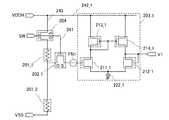
図1は2つの抵抗素子201_1、抵抗素子201_2を用いて電位V1を出力する電位
分割回路を有する半導体装置の例である。FIG. 1 illustrates an example of a semiconductor device including a potential divider circuit that outputs a potential V1 using two resistor elements 201_1 and 201_2.
図1に示す半導体装置は、抵抗素子(第1抵抗素子)201_1及び抵抗素子(第2抵抗
素子)201_2が直列に設けられた電源線240と、選択線241と、選択線241と
ゲート端子とが電気的に接続する酸化物半導体層を含むスイッチトランジスタ202_1
と、電源線240とスイッチトランジスタ202_1を介して電気的に接続するトランジ
スタ211_1を含む演算増幅回路203_1とが設けられた電位分割回路を有し、抵抗
素子201_1と抵抗素子201_2とスイッチトランジスタ202_1のソース端子と
が電気的に接続し、スイッチトランジスタ202_1のドレイン端子と演算増幅回路20
3_1に含まれるトランジスタ211_1のゲート端子とが電気的に接続する半導体装置
である。A semiconductor device illustrated in FIG. 1 includes a
And a potential dividing circuit provided with an operational amplifier circuit 203_1 including a transistor 211_1 that is electrically connected to the
3_1 is a semiconductor device which is electrically connected to a gate terminal of a transistor 211_1 included in 3_1.
演算増幅回路203_1は、トランジスタ(第1トランジスタ)211_1及びトランジ
スタ(第2トランジスタ)212_1が設けられた差動入力回路と、トランジスタ(第3
トランジスタ)213_1及びトランジスタ(第4トランジスタ)214_1が設けられ
たカレントミラー回路と、定電流源222_1とを含む。The operational amplifier circuit 203_1 includes a differential input circuit provided with a transistor (first transistor) 211_1 and a transistor (second transistor) 212_1, and a transistor (third transistor).
Transistor) 213_1 and a transistor (fourth transistor) 214_1, and a constant current source 222_1.
トランジスタ211_1のソース端子(第1ソース端子)と、トランジスタ212_1の
ソース端子(第2ソース端子)と、定電流源222_1とが電気的に接続し、トランジス
タ213_1のソース端子(第3ソース端子)と、トランジスタ214_1のソース端子
(第4ソース端子)とが電気的に接続し、トランジスタ211_1のドレイン端子(第1
ドレイン端子)と、トランジスタ213_1のドレイン端子(第3ドレイン端子)と、第
3トランジスタ213_1のゲート端子(第3ゲート端子)と、トランジスタ214_1
のゲート端子(第4ゲート端子)とが電気的に接続し、トランジスタ212_1のゲート
端子(第2ゲート端子)と、トランジスタ212_1のドレイン端子(第2ドレイン端子
)と、トランジスタ214_1のドレイン端子(第4ドレイン端子)とが電気的に接続し
ている。なお、トランジスタ213_1のソース端子(第3ソース端子)とトランジスタ
214_1のソース端子(第4ソース端子)とは高電位VDDが供給される電源線242
_1に電気的に接続されている。The source terminal (first source terminal) of the transistor 211_1, the source terminal (second source terminal) of the transistor 212_1, and the constant current source 222_1 are electrically connected, and the source terminal (third source terminal) of the transistor 213_1 is connected. And the source terminal (fourth source terminal) of the transistor 214_1 are electrically connected to each other, and the drain terminal (first first terminal) of the transistor 211_1
Drain terminal), a drain terminal (third drain terminal) of the transistor 213_1, a gate terminal (third gate terminal) of the third transistor 213_1, and a transistor 214_1.
Is electrically connected to the gate terminal (second gate terminal) of the transistor 212_1, the drain terminal (second drain terminal) of the transistor 212_1, and the drain terminal (second terminal) of the transistor 214_1. 4 drain terminals) are electrically connected. Note that the source terminal (third source terminal) of the transistor 213_1 and the source terminal (fourth source terminal) of the transistor 214_1 are supplied with a
It is electrically connected to _1.
図1に示す半導体装置において、電位分割回路は、電源線240に直列に接続された抵抗
素子201_1、抵抗素子201_2により、電源線240に供給された電位を抵抗分割
し、電源線240と電気的に接続するスイッチトランジスタ202_1を介して所望の分
割された電位V1を出力する。In the semiconductor device illustrated in FIG. 1, the potential dividing circuit divides the potential supplied to the
図2は図1の半導体装置において、電源線240に供給される高電位(VDDH)を、抵
抗素子201_1乃至抵抗素子201_n+1のn+1個の抵抗素子で分割し、V1乃至
Vnのn個の電位を出力する電位分割回路を含む例である。2 shows the semiconductor device of FIG. 1, in which the high potential (VDDH) supplied to the
抵抗素子201_1及び抵抗素子201_2分電圧降下した電位は、酸化物半導体層を用
いたスイッチトランジスタ202_2を介して、トランジスタ(第1トランジスタ)21
1_2及びトランジスタ(第2トランジスタ)212_2が設けられた差動入力回路と、
トランジスタ(第3トランジスタ)213_2及びトランジスタ(第4トランジスタ)2
14_2が設けられたカレントミラー回路と、定電流源222_2とを含む演算増幅回路
203_2より電位V2として出力される。The potentials of the voltage drop by the resistance element 201_1 and the resistance element 201_2 are supplied to the transistor (first transistor) 21 through the switch transistor 202_2 using the oxide semiconductor layer.
A differential input circuit provided with 1_2 and a transistor (second transistor) 212_2;
Transistor (third transistor) 213_2 and transistor (fourth transistor) 2
14_2 is output as a potential V2 from an operational amplifier circuit 203_2 including a current mirror circuit provided with 14_2 and a constant current source 222_2.
同様に、抵抗素子201_1乃至抵抗素子201_n分電圧降下した電位は、酸化物半導
体層を用いたスイッチトランジスタ202_nを介して、トランジスタ(第1トランジス
タ)211_n及びトランジスタ(第2トランジスタ)212_nが設けられた差動入力
回路と、トランジスタ(第3トランジスタ)213_n及びトランジスタ(第4トランジ
スタ)214_nが設けられたカレントミラー回路と、定電流源222_nとを含む演算
増幅回路203_nより電位Vnとして出力される。Similarly, the potentials of the voltage drops by the resistance elements 201_1 to 201_n are provided by the transistor (first transistor) 211_n and the transistor (second transistor) 212_n through the switch transistor 202_n using the oxide semiconductor layer. A potential Vn is output from an operational amplifier circuit 203_n including a differential input circuit, a current mirror circuit provided with a transistor (third transistor) 213_n and a transistor (fourth transistor) 214_n, and a constant current source 222_n.
本明細書において、スイッチトランジスタ202_1乃至202_nのドレイン端子とト
ランジスタ211_1乃至211_nのゲート端子が電気的に接続される部位をそれぞれ
フローティングノード(ノードFN1乃至FNn)と呼ぶ。In this specification, portions where the drain terminals of the switch transistors 202_1 to 202_n and the gate terminals of the transistors 211_1 to 211_n are electrically connected are referred to as floating nodes (nodes FN1 to FNn), respectively.
なお、本明細書に開示する発明において、電源線242_1には、ノードFN1の電位よ
りも高い電位VDDを供給する。Note that in the invention disclosed in this specification, the potential VDD higher than the potential of the node FN1 is supplied to the power supply line 242_1.
スイッチトランジスタ202_1乃至202_nがオフの場合、当該ノードFN1乃至F
Nnは絶縁体中に埋設されたとみなすことができ、ノードFN1乃至FNnには電位が保
持される。酸化物半導体層を用いたスイッチトランジスタ202_1乃至202_nのオ
フ電流は、シリコン半導体などで形成されるトランジスタの10万分の1以下である(例
えば室温(25℃)でのオフ電流が10zA(1zA(ゼプトアンペア)は1×10⁻²
1A)以下)ため、スイッチトランジスタ202_1乃至202_nのリークによる、ノ
ードFN1乃至FNnに保持された電位の低下をほぼ無視することができる。つまり、酸
化物半導体層を用いたスイッチトランジスタ202_1乃至202_nにより、長期間に
わたって電位を保持することが可能である。When the switch transistors 202_1 to 202_n are off, the nodes FN1 to F
Nn can be regarded as being embedded in an insulator, and potentials are held in the nodes FN1 to FNn. The off-state current of the switch transistors 202_1 to 202_n including an oxide semiconductor layer is 1 / 100,000 or less of a transistor formed using a silicon semiconductor or the like (for example, the off-state current at room temperature (25 ° C.) is 10 zA (1 zA (zepto Ampere) is 1 × 10⁻²
1 A) or lower) Therefore, a decrease in potential held at the nodes FN1 to FNn due to leakage of the switch transistors 202_1 to 202_n can be almost ignored. That is, the switch transistors 202_1 to 202_n including the oxide semiconductor layer can hold a potential for a long time.
よって、半導体装置において、電源線240への電位VDDHの供給を連続的に行わなく
てもよく、電源線240への電位VDDHの供給停止期間を設けることができるため、消
費電力を軽減することができる。Therefore, in the semiconductor device, the supply of the potential VDDH to the
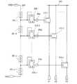
また、図3に示すように、電源線240は酸化物半導体層を含むトランジスタ204を有
し、電源線240に供給された電位は、酸化物半導体層を含むトランジスタ204を介し
て、抵抗素子201_1及び抵抗素子201_2に供給されてもよい。電源線240に設
けられる酸化物半導体層を含むトランジスタ204のゲート端子と、スイッチトランジス
タ202_1のゲート端子とが電気的に接続する構成とすることができる。In addition, as illustrated in FIG. 3, the
酸化物半導体層を含むトランジスタ204を電源線240に設けることで、抵抗素子20
1_1及び抵抗素子201_2への電位の供給を制御することができる。例えば、ノード
FN1に電位を供給した後、スイッチトランジスタ202_1をオフ状態としてノードF
N1に電位を保持する期間、酸化物半導体層を含むトランジスタ204もオフ状態として
電源線240への電位の供給を停止することができる。図3で示す構成であれば、電源線
240への電位の供給を停止する間も、電源線242_1には電位を供給することができ
る。By providing the
The supply of potential to 1_1 and the resistance element 201_2 can be controlled. For example, after a potential is supplied to the node FN1, the switch transistor 202_1 is turned off and the node F
During the period in which the potential is held at N1, the
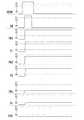
図2に示す半導体装置のより詳細な駆動方法(動作)を図8のタイミングチャートを用い
て説明する。タイミングチャート中のVDDH、SW、FN1等の名称は、図2と対応し
ている。A more detailed driving method (operation) of the semiconductor device shown in FIG. 2 will be described with reference to the timing chart of FIG. Names such as VDDH, SW, and FN1 in the timing chart correspond to those in FIG.
半導体装置の動作を説明するに当たり、演算増幅回路203_1乃至203_nが有する
トランジスタ211_1乃至211_n、212_1乃至212_n、213_1乃至2
13_nおよび214_1乃至214_nは、チャネル幅、チャネル長が同じであり、ト
ランジスタの特性は同じであるとする。In describing operation of the semiconductor device, transistors 211_1 to 211_n, 212_1 to 212_n, and 213_1 to 2 included in the operational amplifier circuits 203_1 to 203_n are included.
13_n and 214_1 to 214_n have the same channel width and channel length, and the same transistor characteristics.
電源線240およびVSSに電位を印加すると、電源線240とVSS間に電流が流れる
。例えば、スイッチトランジスタ202_1のソース端子の電位は、電源線240の電位
よりも抵抗素子201_1の抵抗値と電源線240とVSSの間に流れた電流から算出さ
れる電圧だけ電圧降下した電位となる。選択線SWはスイッチトランジスタ202_1乃
至202_nのゲート端子に電気的に接続されており、スイッチトランジスタ202_1
乃至202_nのソース端子とドレイン端子が導通状態(オン状態)になるように選択線
SWに電圧を印加すると、スイッチトランジスタ202_1乃至202_nの各ドレイン
端子(FN1乃至FNn)に電位が供給される。各ドレイン端子(FN1乃至FNn)の
電位が安定した時点で、スイッチトランジスタ202_1乃至202_nのソース端子と
ドレイン端子が非導通状態(オフ状態)になるように選択線SWに電圧を印加する。When a potential is applied to the
When a voltage is applied to the selection line SW so that the source terminal and the drain terminal of 202 to n are in a conductive state (on state), a potential is supplied to each drain terminal (FN1 to FNn) of the switch transistors 202_1 to 202_n. When the potentials of the drain terminals (FN1 to FNn) are stabilized, a voltage is applied to the selection line SW so that the source terminals and the drain terminals of the switch transistors 202_1 to 202_n are turned off (off state).
演算増幅回路203_1が有するトランジスタ211_1のゲート端子にはFN1の電位
が印加される。そして、トランジスタ211_1には、ゲート端子の電位FN1とソース
端子の電位の差に相当する電流が、ドレイン端子からソース端子に流れる。トランジスタ
213_1とトランジスタ211_1は定電流源222_1を介して、電源線242_1
とGNDに接続されているので、トランジスタ211_1のドレイン端子からソース端子
に流れる電流とトランジスタ213_1のソース端子からドレイン端子に流れる電流は同
じとなる。The potential of FN1 is applied to the gate terminal of the transistor 211_1 included in the operational amplifier circuit 203_1. In the transistor 211_1, a current corresponding to the difference between the potential FN1 of the gate terminal and the potential of the source terminal flows from the drain terminal to the source terminal. The transistor 213_1 and the transistor 211_1 are connected to the power supply line 242_1 through the constant current source 222_1.
Therefore, the current flowing from the drain terminal of the transistor 211_1 to the source terminal is the same as the current flowing from the source terminal of the transistor 213_1 to the drain terminal.
また、トランジスタ213_1のゲート端子およびドレイン端子とトランジスタ214_
1のゲート端子は電気的に接続されており、それぞれのソース端子も電源線242_1に
接続されていることから、トランジスタ213_1のソース端子からドレイン端子に流れ
る電流とトランジスタ214_1のソース端子からドレイン端子に流れる電流は同じとな
る(カレントミラー回路)。なお、前述のトランジスタ213_1とトランジスタ211
_1の関係と同じ理由で、トランジスタ214_1のソース端子からドレイン端子に流れ
る電流とトランジスタ212_1のドレイン端子からソース端子に流れる電流は同じとな
る。In addition, the gate terminal and the drain terminal of the transistor 213_1 and the transistor 214_
Since the gate terminal of 1 is electrically connected and each source terminal is also connected to the power supply line 242_1, current flowing from the source terminal to the drain terminal of the transistor 213_1 and from the source terminal to the drain terminal of the transistor 214_1 The flowing current is the same (current mirror circuit). Note that the transistor 213_1 and the
For the same reason as the relationship _1, the current flowing from the source terminal to the drain terminal of the transistor 214_1 is the same as the current flowing from the drain terminal to the source terminal of the transistor 212_1.
よって、トランジスタ211_1のドレイン端子からソース端子に流れる電流とトランジ
スタ212_1のドレイン端子からソース端子に流れる電流は同じになり、トランジスタ
211_1のソース端子とトランジスタ212_1のソース端子は定電流源222_1に
電気的に接続されていることから、トランジスタ211_1のゲート端子の電位とトラン
ジスタ212_1のゲート端子の電位は同じになる。トランジスタ211_1のゲート端
子の電位はFN1であることから、トランジスタ212_1のゲート端子の電位はFN1
となり、V1の電位はFN1となる。Thus, the current flowing from the drain terminal to the source terminal of the transistor 211_1 is the same as the current flowing from the drain terminal to the source terminal of the transistor 212_1. The source terminal of the transistor 211_1 and the source terminal of the transistor 212_1 are electrically connected to the constant current source 222_1. Since they are connected, the potential of the gate terminal of the transistor 211_1 and the potential of the gate terminal of the transistor 212_1 are the same. Since the potential of the gate terminal of the transistor 211_1 is FN1, the potential of the gate terminal of the transistor 212_1 is FN1.
Thus, the potential of V1 becomes FN1.
同様に抵抗素子201_1及び抵抗素子201_2分電圧降下した電位がFN2に供給さ
れ、V2として出力される。順次VDDHより介在する抵抗素子分、それぞれ電圧降下し
た電位がFN3乃至FNnに供給され、V3乃至Vnとして出力される。Similarly, the potentials of the resistance elements 201_1 and 201_2 are supplied to FN2 and output as V2. Sequentially, the potentials dropped by the resistance elements intervening from VDDH are supplied to FN3 to FNn and output as V3 to Vn.
図6(A)(B)及び図7(A)(B)に電位分割回路を有する半導体装置の他の一形態
を示す。図6(A)(B)及び図7(A)(B)は図1と対応しているが、これに限定さ
れず、図3の構成とも対応することができる。FIGS. 6A and 6B and FIGS. 7A and 7B illustrate another embodiment of a semiconductor device having a potential divider circuit. FIGS. 6A and 6B and FIGS. 7A and 7B correspond to FIG. 1, but are not limited thereto, and can correspond to the configuration of FIG. 3.
図6(A)は、図1における定電流源222_1を抵抗素子217_1とトランジスタ2
15_1及びトランジスタ216_1で作製した構成である。トランジスタ216_1と
トランジスタ215_1はカレントミラー回路を構成しており、トランジスタ215_1
とトランジスタ216_1とには同じ電流が流れる。なお、トランジスタ215_1とト
ランジスタ216_1のチャネル幅、チャネル長は同じであり、トランジスタの特性は同
じであるとする。FIG. 6A illustrates a constant current source 222_1 in FIG.
15_1 and the transistor 216_1 are manufactured. The transistor 216_1 and the transistor 215_1 form a current mirror circuit, and the transistor 215_1
The same current flows through the transistor 216_1. Note that the transistor 215_1 and the transistor 216_1 have the same channel width and channel length, and the transistor has the same characteristics.
図6(B)は、図6(A)にトランジスタ220_1、トランジスタ218_1、容量素
子219_1を含む増幅回路を加える構成である。増幅回路内で使われている容量素子2
19_1は位相補償用容量素子と言い、演算増幅回路203_1が発振しないようにする
ために接続されている。6B illustrates a structure in which an amplifier circuit including a transistor 220_1, a transistor 218_1, and a capacitor 219_1 is added to FIG.
Reference numeral 19_1 denotes a phase compensation capacitive element, which is connected to prevent the operational amplifier circuit 203_1 from oscillating.
図7(A)(B)は演算増幅回路203_1を発振させないために位相の補償、ゲインの
調整を行うため、図7(A)においては抵抗素子205_1と容量素子206_1を挿入
する例であり、図7(B)においては抵抗素子207_1、抵抗素子209_1、及び容
量素子208_1を挿入する例である。FIGS. 7A and 7B are examples in which a resistive element 205_1 and a capacitive element 206_1 are inserted in FIG. 7A in order to perform phase compensation and gain adjustment in order not to oscillate the operational amplifier circuit 203_1. FIG. 7B illustrates an example in which the resistor 207_1, the resistor 209_1, and the capacitor 208_1 are inserted.
本明細書に開示する半導体装置の演算増幅回路には酸化物半導体以外の材料を用いたトラ
ンジスタを用いることができる。酸化物半導体以外の材料を用いたトランジスタは、十分
な高速動作が可能であるため、これを、酸化物半導体層を用いたトランジスタと組み合わ
せて用いることにより、半導体装置の動作の高速性を十分に確保することができる。また
、酸化物半導体以外の材料を用いたトランジスタにより、高速動作が要求される各種回路
(論理回路、駆動回路など)を好適に実現することが可能である。A transistor using a material other than an oxide semiconductor can be used for the operational amplifier circuit of the semiconductor device disclosed in this specification. Since a transistor using a material other than an oxide semiconductor can operate at a sufficiently high speed, the use of this in combination with a transistor including an oxide semiconductor layer can sufficiently increase the operation speed of a semiconductor device. Can be secured. In addition, a transistor including a material other than an oxide semiconductor can favorably realize various circuits (such as a logic circuit and a driver circuit) that are required to operate at high speed.
このように、酸化物半導体以外の材料を用いたトランジスタ(より広義には、十分な高速
動作が可能なトランジスタ)と、酸化物半導体層を用いたトランジスタ(より広義には、
十分にオフ電流が小さいトランジスタ)とを一体に備えることで、これまでにない特徴を
有する半導体装置を実現することができる。Thus, a transistor using a material other than an oxide semiconductor (a transistor capable of high-speed operation in a broad sense) and a transistor including an oxide semiconductor layer (in a broader sense,
And a transistor having a sufficiently low off-state current), a semiconductor device having unprecedented characteristics can be realized.
電源線に直列に接続された複数の抵抗素子により、電源線に供給された電位を抵抗分割し
、電源線と電気的に接続するスイッチトランジスタを介して所望の分割された電位を出力
する電位分割回路を有する半導体装置において、スイッチトランジスタのドレイン端子は
出力側の演算増幅回路に設けられたトランジスタのゲート端子と電気的に接続しノードを
構成する。A potential divider that divides the potential supplied to the power supply line by a plurality of resistance elements connected in series to the power supply line and outputs a desired divided potential via a switch transistor electrically connected to the power supply line In a semiconductor device having a circuit, a drain terminal of a switch transistor is electrically connected to a gate terminal of a transistor provided in an operational amplifier circuit on an output side to form a node.
該ノードに所望の分割された電位を保持することによって、電源線からの電位の供給が停
止されても、電位を出力することができる。By holding a desired divided potential at the node, the potential can be output even when the supply of the potential from the power supply line is stopped.
よって、電源線への電位の供給を連続的に行わなくてもよく、電源線への電位の供給停止
期間を設けることができるため、半導体装置、半導体装置の駆動方法において消費電力を
軽減することができる。Accordingly, it is not necessary to continuously supply potential to the power supply line, and a period for stopping supply of potential to the power supply line can be provided. Therefore, power consumption can be reduced in the semiconductor device and the driving method of the semiconductor device. Can do.
スイッチトランジスタに用いる酸化物半導体層を用いたトランジスタはオフ電流が極めて
小さいため、長期にわたり電位を保持することが可能である。よって、電位の供給を停止
する期間を設けることが可能となり、常に電位を供給する場合と比較して、消費電力を十
分に低減することができる。A transistor including an oxide semiconductor layer used for a switch transistor has extremely low off-state current, and thus can hold a potential for a long time. Therefore, it is possible to provide a period in which the supply of potential is stopped, and power consumption can be sufficiently reduced as compared with the case where the potential is always supplied.
以上、本実施の形態に示す構成、方法などは、他の実施の形態に示す構成、方法などと適
宜組み合わせて用いることができる。The structures, methods, and the like described in this embodiment can be combined as appropriate with any of the structures, methods, and the like described in the other embodiments.
(実施の形態2)
本実施の形態では、開示する発明の他の一態様に係る半導体装置の回路構成および駆動方
法について、図4及び図5を参照して説明する。(Embodiment 2)
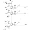
In this embodiment, a circuit configuration and a driving method of a semiconductor device according to another embodiment of the disclosed invention will be described with reference to FIGS.
図4及び図5は実施の形態1に示した図2の半導体装置において、演算増幅回路の代わり
に容量素子を設けた例であり、実施の形態1と同一部分又は同様な機能を有する部分は、
実施の形態1と同様であり、繰り返しの説明は省略する。また同じ箇所の詳細な説明は省
略する。4 and 5 are examples in which a capacitor element is provided instead of the operational amplifier circuit in the semiconductor device of FIG. 2 shown in
This is the same as in
図4は、電源線240に供給される高電位(VDDH)を、抵抗素子201_1乃至抵抗
素子201_n+1のn+1個の抵抗素子で分割し、V1乃至Vnのn個の電位を出力す
る電位分割回路を含む例である。FIG. 4 illustrates a potential dividing circuit that divides a high potential (VDDH) supplied to the
抵抗素子201_1乃至抵抗素子201_n+1が直列に設けられた電源線240と、選
択線241と、選択線241とゲート端子とが電気的に接続する酸化物半導体層を含むス
イッチトランジスタ202_1乃至スイッチトランジスタ202_nと、電源線240と
スイッチトランジスタ202_1乃至スイッチトランジスタ202_nを介してそれぞれ
電気的に接続する容量素子223_1乃至223_nとが設けられた電位分割回路を有し
、抵抗素子201_1乃至抵抗素子201_n+1とスイッチトランジスタ202_1乃
至スイッチトランジスタ202_nのソース端子とが電気的に接続し、スイッチトランジ
スタ202_1乃至スイッチトランジスタ202_nのドレイン端子と容量素子223_
1乃至223_nの一方の端子とが電気的に接続する半導体装置である。A
The semiconductor device is electrically connected to one terminal of 1 to 223 — n.
本実施の形態では、スイッチトランジスタ202_1乃至スイッチトランジスタ202_
nのドレイン端子は容量素子223_1乃至223_nの一方の端子と電気的に接続しノ
ード(FN1乃至FNn)をそれぞれ構成する。In this embodiment, the switch transistors 202_1 to 202_
The drain terminal of n is electrically connected to one terminal of the capacitors 223_1 to 223_n to form nodes (FN1 to FNn), respectively.
スイッチトランジスタ202_1乃至スイッチトランジスタ202_nをオン状態として
電源線240から抵抗素子201_1乃至抵抗素子201_n+1により電位V1乃至V
nに分割された電位をノードFN1乃至FNnに供給(蓄積)する。電位V1乃至Vnの
供給後は、スイッチトランジスタ202_1乃至スイッチトランジスタ202_nをオフ
状態とし、ノードFN1乃至FNnに電位を保持する。ノードFN1乃至FNnに電位V
1乃至Vnを保持することによって、電源線240からの電位の供給が停止されても、電
位V1乃至Vnを出力することができる。The switch transistors 202_1 to 202_n are turned on, and the potentials V1 to V are supplied from the
The potential divided into n is supplied (stored) to the nodes FN1 to FNn. After the potentials V1 to Vn are supplied, the switch transistors 202_1 to 202_n are turned off, and the potentials are held in the nodes FN1 to FNn. The potential V is applied to the nodes FN1 to FNn.
By holding 1 to Vn, the potentials V1 to Vn can be output even when the supply of the potential from the
なお、本実施の形態の構成では、図5に示すように、容量素子223_1より出力側に、
配線等に起因する抵抗素子224_1が形成され、容量素子225_1が必然的に負荷さ
れている。スイッチトランジスタ202_1乃至スイッチトランジスタ202_nのドレ
イン端子と容量素子223_1乃至223_nの一方の端子とが電気的に接続することで
構成するノード(FN1乃至FNn)に電位V1乃至Vnを保持するためには、容量素子
223_1の容量C1は、寄生容量である容量素子225_1の容量C2より十分に大き
くする必要がある。Note that in the structure of this embodiment, as illustrated in FIG. 5, the output side of the capacitor 223 </ b> _ <b> 1 is
A resistance element 224_1 resulting from wiring or the like is formed, and the capacitor 225_1 is inevitably loaded. In order to hold the potentials V1 to Vn at nodes (FN1 to FNn) formed by electrically connecting the drain terminals of the switch transistors 202_1 to 202_n and one of the terminals of the capacitors 223_1 to 223_n, capacitors The capacitor C1 of the element 223_1 needs to be sufficiently larger than the capacitor C2 of the capacitor 225_1 that is a parasitic capacitor.
また、本実施の形態の図4の構成においても、図3に示すように、電源線240は酸化物
半導体層を含むトランジスタ204を有し、電源線240に供給された電位は、酸化物半
導体層を含むトランジスタ204を介して、抵抗素子201_1乃至抵抗素子201_n
+1に供給されてもよい。また、電源線240に設けられる酸化物半導体層を含むトラン
ジスタ204のゲート端子と、スイッチトランジスタ202_1乃至スイッチトランジス
タ202_nのゲート端子とが電気的に接続する構成とすることができる。In the structure of FIG. 4 in this embodiment mode, as shown in FIG. 3, the
+1 may be supplied. The gate terminal of the
酸化物半導体層を含むトランジスタ204を電源線240に設けることで、抵抗素子20
1_1乃至抵抗素子201_n+1への電位の供給を制御することができる。例えば、ノ
ードFN1乃至FNnに電位を供給した後、スイッチトランジスタ202_1乃至スイッ
チトランジスタ202_nをオフ状態としてノードFN1乃至FNnに電位を保持する期
間、酸化物半導体層を含むトランジスタ204もオフ状態として電源線240への電位の
供給を停止することができる。By providing the
The supply of potential to 1_1 to the resistor 201_n + 1 can be controlled. For example, after the potentials are supplied to the nodes FN1 to FNn, the switch transistors 202_1 to 202_n are turned off and the potentials are held in the nodes FN1 to FNn, and the
なお、本実施の形態の半導体装置は、初期状態ではV1乃至Vnはフローティングとなっ
ており、電位が不定となっている。図4には図示していないが、容量素子223_1乃至
223_nの出力側の各末端、つまり、V1乃至Vnが供給される各配線の末端には、酸
化物半導体層を含むスイッチトランジスタA1乃至Anの各ドレイン端子が電気的に接続
されている。スイッチトランジスタA1乃至Anの各ゲート端子は制御線に接続され、各
ソース端子はVSSに接続されている。そして、制御線を制御することで、酸化物半導体
層を含むスイッチトランジスタA1乃至Anのゲート端子を制御して、スイッチトランジ
スタA1乃至Anを導通状態にし、V1乃至Vnが供給される各配線をVSSと同じ電位
にするようになっている。そして、V1乃至Vnが供給される各配線がVSSと同じ電位
になったら、再度、制御線を制御することで、酸化物半導体層を含むスイッチトランジス
タA1乃至Anのゲート端子を制御して、スイッチトランジスタA1乃至Anを非導通状
態(オフ状態)にする。そして、選択線SWに電位を与えることで、スイッチトランジス
タ202_1乃至202_nが導通状態(オン状態)になり、FN1乃至FNnの電位が
確定し、容量素子223_1乃至223_nを介して、各配線にV1乃至Vnが供給され
る。Note that in the semiconductor device of this embodiment, V1 to Vn are floating in the initial state, and the potential is indefinite. Although not illustrated in FIG. 4, switch transistors A1 to An including oxide semiconductor layers are provided at the output terminals of the capacitors 223_1 to 223_n, that is, to the terminals of the wirings to which V1 to Vn are supplied. Each drain terminal is electrically connected. Each gate terminal of the switch transistors A1 to An is connected to a control line, and each source terminal is connected to VSS. Then, by controlling the control line, the gate terminals of the switch transistors A1 to An including the oxide semiconductor layer are controlled, the switch transistors A1 to An are turned on, and the wirings to which V1 to Vn are supplied are set to VSS. Is set to the same potential. When each of the wirings to which V1 to Vn is supplied has the same potential as VSS, the gates of the switch transistors A1 to An including the oxide semiconductor layer are controlled by controlling the control line again, so that the switch The transistors A1 to An are turned off (off state). Then, by applying a potential to the selection line SW, the switch transistors 202_1 to 202_n are turned on (on state), the potentials of FN1 to FNn are determined, and the wirings V1 to V1 are connected to the wirings through the capacitor elements 223_1 to 223_n. Vn is supplied.
以上のように、ノードFN1乃至FNnに所望の分割された電位V1乃至Vnを保持する
ことによって、電源線240からの電位の供給が停止されても、電位V1乃至Vnを出力
することができる。As described above, by holding the desired divided potentials V1 to Vn at the nodes FN1 to FNn, the potentials V1 to Vn can be output even when the supply of the potential from the
よって、電源線240への電位の供給を連続的に行わなくてもよく、電源線への電位の供
給停止期間を設けることができるため、半導体装置、半導体装置の駆動方法において消費
電力を軽減することができる。Accordingly, it is not necessary to continuously supply the potential to the
スイッチトランジスタに用いる酸化物半導体層を用いたトランジスタはオフ電流が極めて
小さいため、長期にわたり電位を保持することが可能である。よって、電位の供給を停止
する期間を設けることが可能となり、常に電位を供給する場合と比較して、消費電力を十
分に低減することができる。A transistor including an oxide semiconductor layer used for a switch transistor has extremely low off-state current, and thus can hold a potential for a long time. Therefore, it is possible to provide a period in which the supply of potential is stopped, and power consumption can be sufficiently reduced as compared with the case where the potential is always supplied.
以上、本実施の形態に示す構成、方法などは、他の実施の形態に示す構成、方法などと適
宜組み合わせて用いることができる。The structures, methods, and the like described in this embodiment can be combined as appropriate with any of the structures, methods, and the like described in the other embodiments.
(実施の形態3)
本実施の形態では、開示する発明の他の一態様に係る半導体装置の回路構成および駆動方
法について、図9を参照して説明する。(Embodiment 3)
In this embodiment, a circuit configuration and a driving method of a semiconductor device according to another embodiment of the disclosed invention will be described with reference to FIGS.
図9は実施の形態1に示した図2の半導体装置において、選択線によってオンオフを制御
するスイッチトランジスタの代わりにゲート端子とソース端子とが電気的に接続されたト
ランジスタを用いる例であり、実施の形態1と同一部分又は同様な機能を有する部分は、
実施の形態1と同様であり、繰り返しの説明は省略する。また同じ箇所の詳細な説明は省
略する。FIG. 9 shows an example in which a transistor in which a gate terminal and a source terminal are electrically connected is used instead of a switch transistor that controls on / off by a selection line in the semiconductor device of FIG. 2 described in
This is the same as in
図9は、電源線240に供給される高電位(VDDH)を、抵抗素子201_1乃至抵抗
素子201_n+1のn+1個の抵抗素子で分割し、分割した電位を用いて電源線245
からV1’乃至Vn’のn個の電位を出力する電位分割回路を含む例である。In FIG. 9, a high potential (VDDH) supplied to the
In this example, the potential dividing circuit outputs n potentials V1 ′ to Vn ′.
抵抗素子201_1乃至抵抗素子201_n+1が直列に設けられた電源線240と、ゲ
ート端子とが電気的に接続する酸化物半導体層を含み、且つゲート端子とソース端子とが
電気的に接続されたトランジスタ232_1乃至トランジスタ232_nと、電源線24
0とトランジスタ232_1乃至トランジスタ232_nを介してそれぞれ電気的に接続
するトランジスタ233_1乃至トランジスタ233_nとが設けられた電位分割回路を
有し、抵抗素子201_1乃至抵抗素子201_n+1とトランジスタ232_1乃至ト
ランジスタ232_nのソース端子とが電気的に接続し、トランジスタ232_1乃至ト
ランジスタ232_nのドレイン端子とトランジスタ233_1乃至トランジスタ233
_nのゲート端子とが電気的に接続する半導体装置である。なお、トランジスタ233_
1乃至トランジスタ233_nは電源線245と電気的に接続している。A transistor 232_1 including an oxide semiconductor layer in which the
0 and transistors 233_1 to 233_n that are electrically connected to each other through the transistors 232_1 to 232_n, respectively, and the resistance elements 201_1 to 201_n + 1 and the source terminals of the transistors 232_1 to 232_n Are electrically connected to each other, and the drain terminals of the transistors 232_1 to 232_n and the transistors 233_1 to 233 are connected.
The semiconductor device is electrically connected to the gate terminal of _n. Note that the transistor 233_
The first to transistors 233 — n are electrically connected to the
本実施の形態では、トランジスタ232_1乃至トランジスタ232_nのドレイン端子
はトランジスタ233_1乃至トランジスタ233_nのゲート端子と電気的に接続しノ
ード(FN1乃至FNn)をそれぞれ構成する。In this embodiment, the drain terminals of the transistors 232_1 to 232_n are electrically connected to the gate terminals of the transistors 233_1 to 233_n to form nodes (FN1 to FNn), respectively.
トランジスタ232_1乃至トランジスタ232_nをオン状態として電源線240から
抵抗素子201_1乃至抵抗素子201_n+1により所望の電位に分割された電位をノ
ードFN1乃至FNnに供給(蓄積)する。所望の電位の供給後は、トランジスタ232
_1乃至トランジスタ232_nはオフ状態となり、ノードFN1乃至FNnに電位を保
持する。ノードFN1乃至FNnに所望の電位を保持することによって、電源線240か
らの電位の供給が停止されても、トランジスタ233_1乃至トランジスタ233_nの
ゲート端子に所望の電位を供給することができるので、電源線245より電位V1’乃至
Vn’を出力することができる。The transistors 232_1 to 232_n are turned on, and potentials divided into desired potentials by the resistance elements 201_1 to 201_n + 1 from the
_1 to 232_n are off and hold potentials at the nodes FN1 to FNn. By holding a desired potential in the nodes FN1 to FNn, a desired potential can be supplied to the gate terminals of the transistors 233_1 to 233_n even when supply of potential from the
また、本実施の形態の図9の構成においても、図3に示すように、電源線240は酸化物
半導体層を含むトランジスタ204を有し、電源線240に供給された電位は、酸化物半
導体層を含むトランジスタ204を介して、抵抗素子201_1乃至抵抗素子201_n
+1に供給されてもよい。9 as well, the
+1 may be supplied.
酸化物半導体層を含むトランジスタ204を電源線240に設けることで、抵抗素子20
1_1乃至抵抗素子201_n+1への電位の供給を制御することができる。例えば、ノ
ードFN1乃至FNnに電位を供給した後、トランジスタ232_1乃至トランジスタ2
32_nがオフ状態となりノードFN1乃至FNnに電位を保持する期間、酸化物半導体
層を含むトランジスタ204もオフ状態として電源線240への電位の供給を停止するこ
とができる。By providing the
The supply of potential to 1_1 to the resistor 201_n + 1 can be controlled. For example, after potentials are supplied to the nodes FN1 to FNn, the transistors 232_1 to 2 are supplied.
In the period in which 32_n is off and the potentials of the nodes FN1 to FNn are held, the
以上のように、ノードFN1乃至FNnに所望の分割された電位を保持することによって
、電源線240からの電位の供給が停止されても、電位V1’乃至Vn’を出力すること
ができる。As described above, by holding desired divided potentials at the nodes FN1 to FNn, the potentials V1 ′ to Vn ′ can be output even when the supply of the potential from the
よって、電源線240への電位の供給を連続的に行わなくてもよく、電源線への電位の供
給停止期間を設けることができるため、半導体装置、半導体装置の駆動方法において消費
電力を軽減することができる。Accordingly, it is not necessary to continuously supply the potential to the
トランジスタ232_1乃至トランジスタ232_nに用いる、酸化物半導体層を用いた
トランジスタはオフ電流が極めて小さいため、長期にわたり電位を保持することが可能で
ある。よって、電位の供給を停止する期間を設けることが可能となり、常に電位を供給す
る場合と比較して、消費電力を十分に低減することができる。A transistor including an oxide semiconductor layer that is used for the transistors 232_1 to 232_n has extremely low off-state current, and thus can hold a potential for a long time. Therefore, it is possible to provide a period in which the supply of potential is stopped, and power consumption can be sufficiently reduced as compared with the case where the potential is always supplied.
以上、本実施の形態に示す構成、方法などは、他の実施の形態に示す構成、方法などと適
宜組み合わせて用いることができる。The structures, methods, and the like described in this embodiment can be combined as appropriate with any of the structures, methods, and the like described in the other embodiments.
(実施の形態4)
本実施の形態では、開示する発明の一態様に係る半導体装置の構成およびその作製方法に
ついて、図10乃至図12を参照して説明する。(Embodiment 4)
In this embodiment, a structure and a manufacturing method of a semiconductor device according to one embodiment of the disclosed invention will be described with reference to FIGS.
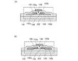
図10(A)および図10(B)は、図1の回路図で示した電位分割回路を有する半導体
装置の構成の一例である。図10(A)には、半導体装置の断面を、図10(B)には、
半導体装置の平面をそれぞれ示す。図10(A)は、図10(B)のA1−A2における
断面図である。なお、図10(B)の平面図においては、絶縁層150、絶縁層152、
及び配線158は省略しており、図面を簡略化している。10A and 10B illustrate an example of a structure of the semiconductor device including the potential dividing circuit illustrated in the circuit diagram of FIG. 10A shows a cross section of the semiconductor device, and FIG.
The plane of a semiconductor device is shown, respectively. FIG. 10A is a cross-sectional view taken along line A1-A2 of FIG. Note that in the plan view of FIG. 10B, the insulating
The
図10(A)および図10(B)に示される半導体装置は、下部に第1の半導体材料を用
いたトランジスタ211_1を有し、上部に第2の半導体材料を用いたスイッチトランジ
スタ202_1を有するものである。The semiconductor device illustrated in FIGS. 10A and 10B includes a transistor 211_1 using a first semiconductor material in a lower portion and a switch transistor 202_1 using a second semiconductor material in an upper portion. It is.
ここで、第1の半導体材料と第2の半導体材料とは異なる材料とすることが望ましい。本
実施の形態では、第1の半導体材料を酸化物半導体以外の半導体材料(シリコンなど)と
し、第2の半導体材料を酸化物半導体とする。酸化物半導体以外の材料を用いたトランジ
スタは、高速動作が容易である。一方で、酸化物半導体を用いたトランジスタは、その特
性により長時間の電位の保持を可能とする。Here, the first semiconductor material and the second semiconductor material are preferably different materials. In this embodiment, the first semiconductor material is a semiconductor material other than an oxide semiconductor (such as silicon), and the second semiconductor material is an oxide semiconductor. A transistor including a material other than an oxide semiconductor can easily operate at high speed. On the other hand, a transistor including an oxide semiconductor can hold a potential for a long time due to its characteristics.
図10(A)および図10(B)におけるトランジスタ211_1は、半導体材料(例え
ば、シリコンなど)を含む基板185に設けられたチャネル形成領域116と、チャネル
形成領域116を挟むように設けられた不純物領域120と、不純物領域120に接する
金属化合物領域124と、チャネル形成領域116上に設けられたゲート絶縁層108と
、ゲート絶縁層108上に設けられたゲート電極110と、を有する。なお、図において
、明示的にはソース電極やドレイン電極を有しない場合があるが、便宜上、このような状
態を含めてトランジスタと呼ぶ場合がある。また、この場合、トランジスタの接続関係を
説明するために、ソース領域やドレイン領域を含めてソース電極やドレイン電極と表現す
ることがある。つまり、本明細書において、ソース電極との記載には、ソース領域が、ド
レイン電極との記載にはドレイン領域が含まれうる。A transistor 211_1 in FIGS. 10A and 10B includes a
また、基板100上にはトランジスタ211_1を囲むように素子分離絶縁層106が設
けられており、トランジスタ211_1を覆うように絶縁層128、絶縁層130が設け
られている。なお、高集積化を実現するためには、図10(A)および図10(B)に示
すようにトランジスタ211_1がサイドウォール絶縁層を有しない構成とすることが望
ましい。一方で、トランジスタ211_1の特性を重視する場合には、ゲート電極110
の側面にサイドウォール絶縁層を設け、不純物濃度が異なる領域を含む不純物領域120
を設けても良い。Further, an element
Sidewall insulating layers are provided on the side surfaces of the
May be provided.
ここで、絶縁層130は、平坦性の良好な表面を有しているのが好ましい。Here, the insulating
図10(A)および図10(B)におけるスイッチトランジスタ202_1は、絶縁層1
30上に形成された酸化物半導体層144と、ソース電極142aおよびドレイン電極1
42bと、酸化物半導体層144及びソース電極142aおよびドレイン電極142bを
覆うゲート絶縁層146と、ゲート絶縁層146上に酸化物半導体層144と重畳するよ
うに設けられたゲート電極148とを有する。なお、ゲート電極148は、図1に示す回
路図に示す選択線241と電気的に接続している。The switch transistor 202_1 in FIGS. 10A and 10B includes the insulating
30 and the
42b, a
ドレイン電極142bはトランジスタ211_1のゲート電極110と接して形成されて
おり、スイッチトランジスタ202_1のドレイン電極142bとトランジスタ211_
1のゲート電極110とが電気的に接続することで、ノード(FN1)を構成する。The
The
ここで、酸化物半導体層144は水素などの不純物が十分に除去され、十分な酸素が供給
されることにより、高純度化されたものであることが望ましい。具体的には、例えば、酸
化物半導体層144の水素濃度は5×10¹⁹atoms/cm3以下、望ましくは5×
1018atoms/cm3以下、より望ましくは5×1017atoms/cm3以下
とする。Here, it is preferable that the
1018 atoms / cm3 or less, more desirably 5 × 10¹⁷ atoms / cm3 or less.
なお、上述の酸化物半導体層144中の水素濃度は、二次イオン質量分析法(SIMS:
Secondary Ion Mass Spectroscopy)で測定されるもの
である。このように、水素濃度が十分に低減され、十分な酸素の供給により酸素欠乏に起
因するエネルギーギャップ中の欠陥準位が低減された酸化物半導体層144では、水素等
のドナーに起因するキャリア密度が1×10¹²/cm3未満、望ましくは、1×101
1/cm3未満、より望ましくは1.45×1010/cm3未満となる。また、例えば
、室温(25℃)でのオフ電流(ここでは、単位チャネル幅(1μm)あたりの値)は1
00zA(1zA(ゼプトアンペア)は1×10⁻²¹A)以下、望ましくは10zA以
下となる。このように、i型化(真性化)または実質的にi型化された酸化物半導体を用
いることで、極めて優れたオフ電流特性のスイッチトランジスタ202_1を得ることが
できる。Note that the hydrogen concentration in the
Measured by Secondary Ion Mass Spectroscopy). As described above, in the
It is less than1 / cm3 , more desirably less than 1.45 × 10¹⁰ / cm3 . Further, for example, the off-current at room temperature (25 ° C.) (here, the value per unit channel width (1 μm)) is 1.
00zA (1zA (zeptoampere) is 1 × 10⁻²¹ A) or less, preferably 10 zA or less. In this manner, by using an i-type (intrinsic) or substantially i-type oxide semiconductor, the switch transistor 202_1 with extremely excellent off-state current characteristics can be obtained.
また、酸化物半導体層144は二次イオン質量分析法で測定される最低値が、ナトリウム
(Na)が5×1016cm−3以下、好ましくは1×1016cm−3以下、さらに好
ましくは1×1015cm−3以下とし、リチウム(Li)が5×1015cm−3以下
、好ましくは1×1015cm−3以下とし、カリウム(K)が5×1015cm−3以
下、好ましくは1×1015cm−3以下とする。The minimum value of the
アルカリ金属、及びアルカリ土類金属は酸化物半導体層144にとっては悪性の不純物で
あり、少ないほうがよい。特にアルカリ金属のうち、Naは酸化物半導体層144に接す
る絶縁膜が酸化物であった場合、その中に拡散し、Na+となる。また、酸化物半導体層
144内において、金属と酸素の結合を分断し、あるいは結合中に割り込む。その結果、
酸化物半導体層144を用いたトランジスタの特性の劣化(例えば、ノーマリオン化(し
きい値の負へのシフト)、移動度の低下等)をもたらす。加えて、特性のばらつきの原因
ともなる。このような問題は、特に酸化物半導体層144中の水素の濃度が十分に低い場
合において顕著となる。したがって、酸化物半導体層144中の水素の濃度が5×101
9cm−3以下、特に5×1018cm−3以下である場合には、アルカリ金属の濃度を
上記の値にすることが強く求められる。Alkali metal and alkaline earth metal are malignant impurities for the
Deterioration of characteristics of the transistor including the oxide semiconductor layer 144 (for example, normalization (threshold shift to negative), reduction in mobility, or the like) is brought about. In addition, it causes variation in characteristics. Such a problem becomes significant particularly when the concentration of hydrogen in the
When it is 9 cm−3 or less, particularly 5 × 1018 cm−3 or less, it is strongly required to set the alkali metal concentration to the above value.
また、絶縁層130の表面であって酸化物半導体層144と接する領域は、その二乗平均
平方根(RMS)粗さを1nm以下とすることが好ましい。このように、二乗平均平方根
(RMS)粗さが1nm以下という極めて平坦な領域にスイッチトランジスタ202_1
のチャネル形成領域を設けることにより、スイッチトランジスタ202_1が微細化され
る状況においても、短チャネル効果などの不具合を防止し、良好な特性を有するスイッチ
トランジスタ202_1を提供することが可能である。Further, it is preferable that the surface of the insulating
By providing the channel formation region, it is possible to provide a switch transistor 202_1 having favorable characteristics by preventing problems such as a short channel effect even in a situation where the switch transistor 202_1 is miniaturized.
スイッチトランジスタ202_1とトランジスタ211_1とを積層構造とすることによ
って半導体装置に占める占有面積を縮小することができる。よって、半導体装置の高集積
化を図ることができる。With the stacked structure of the switch transistor 202_1 and the transistor 211_1, the area occupied by the semiconductor device can be reduced. Therefore, high integration of the semiconductor device can be achieved.
スイッチトランジスタ202_1の上には、絶縁層150が設けられており、絶縁層15
0上には絶縁層152が設けられている。ゲート絶縁層146、絶縁層150及び絶縁層
152にはソース電極142aに達する開口が形成され、該開口には電極156が形成さ
れている。絶縁層152上に、絶縁層152に埋め込まれるように形成された電極156
に接して配線158を形成することで、ソース電極142aと配線158とが電気的に接
続している。ここで、配線158は、図1に示す回路において電源線240、又は電源線
240と電気的に接続する配線である。An insulating
An insulating
The
なお、開示する発明に係る半導体装置の構成は、図10(A)および図10(B)に示さ
れるものに限定されない。開示する発明の一態様の技術的思想は、酸化物半導体と、酸化
物半導体以外の材料と、を用いた積層構造を形成する点にあるから、電極の接続関係等の
詳細については、適宜変更することができる。Note that the structure of the semiconductor device according to the disclosed invention is not limited to that illustrated in FIGS. Since the technical idea of one embodiment of the disclosed invention is to form a stacked structure using an oxide semiconductor and a material other than the oxide semiconductor, details of electrode connection relations and the like are changed as appropriate. can do.
次に、上記半導体装置の作製方法の一例について説明する。以下では、はじめに下部のト
ランジスタ211_1の作製方法について図11を参照して説明し、その後、上部のスイ
ッチトランジスタ202_1および容量素子164の作製方法について図12および図1
3を参照して説明する。Next, an example of a method for manufacturing the semiconductor device will be described. Hereinafter, a method for manufacturing the lower transistor 211_1 will be described with reference to FIGS. 11A to 11C, and then, a method for manufacturing the upper switch transistor 202_1 and the capacitor 164 will be described with reference to FIGS.
This will be described with reference to FIG.
まず、半導体材料を含む基板185を用意する(図11(A)参照)。半導体材料を含む
基板185としては、シリコンや炭化シリコンなどの単結晶半導体基板、多結晶半導体基
板、シリコンゲルマニウムなどの化合物半導体基板、SOI基板などを適用することがで
きる。ここでは、半導体材料を含む基板185として、単結晶シリコン基板を用いる場合
の一例について示すものとする。なお、一般に「SOI基板」は、絶縁表面上にシリコン
半導体層が設けられた構成の基板をいうが、本明細書等においては、絶縁表面上にシリコ
ン以外の材料からなる半導体層が設けられた構成の基板も含む概念として用いる。つまり
、「SOI基板」が有する半導体層は、シリコン半導体層に限定されない。また、SOI
基板には、ガラス基板などの絶縁基板上に絶縁層を介して半導体層が設けられた構成のも
のが含まれるものとする。First, a
The substrate includes a substrate in which a semiconductor layer is provided on an insulating substrate such as a glass substrate with an insulating layer interposed therebetween.
半導体材料を含む基板185として、特に、シリコンなどの単結晶半導体基板を用いる場
合には、半導体装置の回路の動作を高速化することができるため好適である。In particular, when a single crystal semiconductor substrate such as silicon is used as the
なお、トランジスタのしきい値電圧を制御するために、後にトランジスタ211_1のチ
ャネル形成領域116となる領域に、不純物元素を添加しても良い。ここでは、トランジ
スタ211_1のしきい値電圧が正となるように導電性を付与する不純物元素を添加する
。半導体材料がシリコンの場合、該導電性を付与する不純物には、例えば、硼素、アルミ
ニウム、ガリウムなどがある。なお、不純物元素の添加後には、加熱処理を行い、不純物
元素の活性化や不純物元素の添加時に生じる欠陥の改善等を図るのが望ましい。Note that an impurity element may be added to a region to be the
基板185に素子分離絶縁層106を形成する(図11(B)参照)。)素子分離絶縁層
106は基板185を選択的に除去し、該除去領域を埋めるように絶縁層を成膜し、選択
的に除去することによって形成することができる。当該絶縁層は、酸化シリコンや窒化シ
リコン、酸化窒化シリコンなどを用いて形成される。絶縁層の除去方法としては、CMP
(化学的機械的研磨)処理などの研磨処理やエッチング処理などがあるが、そのいずれを
用いても良い。なお、素子分離絶縁層106の形成領域以外の基板185は半導体領域と
して用いることができる。The element
There are polishing treatments such as (chemical mechanical polishing) treatment and etching treatment, and any of them may be used. Note that the
次に、基板185の表面に絶縁層を形成し、当該絶縁層上に導電材料を含む層を形成する
。Next, an insulating layer is formed on the surface of the
絶縁層は後のゲート絶縁層となるものであり、例えば、基板185表面の熱処理(熱酸化
処理や熱窒化処理など)によって形成することができる。熱処理に代えて、高密度プラズ
マ処理を適用しても良い。高密度プラズマ処理は、例えば、He、Ar、Kr、Xeなど
の希ガス、酸素、酸化窒素、アンモニア、窒素、水素などの混合ガスを用いて行うことが
できる。もちろん、CVD法やスパッタリング法等を用いて絶縁層を形成しても良い。当
該絶縁層は、酸化シリコン、酸化窒化シリコン、窒化シリコン、酸化ハフニウム、酸化ア
ルミニウム、酸化タンタル、酸化イットリウム、ハフニウムシリケート(HfSixOy
(x>0、y>0))、窒素が添加されたハフニウムシリケート(HfSixOy(x>
0、y>0))、窒素が添加されたハフニウムアルミネート(HfAlxOy(x>0、
y>0))等を含む単層構造または積層構造とすることが望ましい。また、絶縁層の厚さ
は、例えば、1nm以上100nm以下、好ましくは10nm以上50nm以下とするこ
とができる。The insulating layer will be a gate insulating layer later, and can be formed by, for example, heat treatment (thermal oxidation treatment, thermal nitridation treatment, or the like) on the surface of the
(X> 0, y> 0)), hafnium silicate added with nitrogen (HfSix Oy (x>
0, y> 0)), nitrogen added hafnium aluminate (HfAlx Oy (x> 0,
A single-layer structure or a stacked structure including y> 0)) is desirable. The insulating layer can have a thickness of, for example, 1 nm to 100 nm, preferably 10 nm to 50 nm.
導電材料を含む層は、アルミニウムや銅、チタン、タンタル、タングステン等の金属材料
を用いて形成することができる。また、多結晶シリコンなどの半導体材料を用いて、導電
材料を含む層を形成しても良い。形成方法も特に限定されず、蒸着法、CVD法、スパッ
タリング法、スピンコート法などの各種成膜方法を用いることができる。なお、本実施の
形態では、導電材料を含む層を、金属材料を用いて形成する場合の一例について示すもの
とする。The layer including a conductive material can be formed using a metal material such as aluminum, copper, titanium, tantalum, or tungsten. Alternatively, a layer including a conductive material may be formed using a semiconductor material such as polycrystalline silicon. There is no particular limitation on the formation method, and various film formation methods such as an evaporation method, a CVD method, a sputtering method, and a spin coating method can be used. Note that in this embodiment, an example of the case where the layer including a conductive material is formed using a metal material is described.
その後、絶縁層および導電材料を含む層を選択的にエッチングして、ゲート絶縁層108
およびゲート電極110を形成する(図11(C)参照)。After that, the
Then, the
次に、基板185にリン(P)やヒ素(As)などを添加して、チャネル形成領域116
および不純物領域120を形成する。なお、ここではn型トランジスタを形成するために
リンやヒ素を添加しているが、p型トランジスタを形成する場合には、硼素(B)やアル
ミニウム(Al)などの不純物元素を添加すればよい。ここで、添加する不純物の濃度は
適宜設定することができるが、半導体素子が高度に微細化される場合には、その濃度を高
くすることが望ましい。Next, phosphorus (P), arsenic (As), or the like is added to the
And the
なお、ゲート電極110の周囲にサイドウォール絶縁層を形成して、不純物元素が異なる
濃度で添加された不純物領域を形成しても良い。Note that a sidewall insulating layer may be formed around the
次に、ゲート電極110、不純物領域120等を覆うように金属層122を形成する。当
該金属層122は、真空蒸着法やスパッタリング法、スピンコート法などの各種成膜方法
を用いて形成することができる。金属層は、基板185を構成する半導体材料と反応する
ことによって低抵抗な金属化合物となる金属材料を用いて形成することが望ましい。この
ような金属材料としては、例えば、チタン、タンタル、タングステン、ニッケル、コバル
ト、白金等がある。Next, a metal layer 122 is formed so as to cover the
次に、熱処理を施して、上記金属層と半導体材料とを反応させる。これにより、不純物領
域120に接する金属化合物領域124が形成される。なお、ゲート電極110として多
結晶シリコンなどを用いる場合には、ゲート電極110の金属層と接触する部分にも、金
属化合物領域が形成されることになる。Next, heat treatment is performed to react the metal layer with the semiconductor material. As a result, a
上記熱処理としては、例えば、フラッシュランプの照射による熱処理を用いることができ
る。もちろん、その他の熱処理方法を用いても良いが、金属化合物の形成に係る化学反応
の制御性を向上させるためには、ごく短時間の熱処理を実現できる方法を用いることが望
ましい。なお、上記の金属化合物領域は、金属材料と半導体材料との反応により形成され
るものであり、十分に導電性が高められた領域である。当該金属化合物領域を形成するこ
とで、電気抵抗を十分に低減し、素子特性を向上させることができる。なお、金属化合物
領域124を形成した後には、金属層は除去する。As the heat treatment, for example, heat treatment by flash lamp irradiation can be used. Of course, other heat treatment methods may be used, but in order to improve the controllability of the chemical reaction related to the formation of the metal compound, it is desirable to use a method capable of realizing a heat treatment for a very short time. Note that the metal compound region is formed by a reaction between a metal material and a semiconductor material, and is a region in which conductivity is sufficiently increased. By forming the metal compound region, the electrical resistance can be sufficiently reduced and the device characteristics can be improved. Note that the metal layer is removed after the
以上により、半導体材料を含む基板185を用いたトランジスタ211_1が形成される
(図11(D)参照)。このようなトランジスタ211_1は、高速動作が可能であると
いう特徴を有する。Through the above steps, the transistor 211_1 using the
なお、上記の各工程の前後には、さらに電極や配線、半導体層、絶縁層などを形成する工
程を含んでいても良い。例えば、配線の構造として、絶縁層および導電層の積層構造でな
る多層配線構造を採用して、高度に集積化した半導体装置を実現することも可能である。Note that before and after each of the above steps, a step of forming an electrode, a wiring, a semiconductor layer, an insulating layer, or the like may be further included. For example, a highly integrated semiconductor device can be realized by adopting a multilayer wiring structure including a laminated structure of an insulating layer and a conductive layer as a wiring structure.
次に、上述の工程により形成された各構成を覆うように、絶縁層128及び絶縁層130
を形成する。絶縁層128、絶縁層130は、酸化シリコン、酸化窒化シリコン、窒化シ
リコン、酸化アルミニウム等の無機絶縁材料を含む材料を用いて形成することができる。
特に、絶縁層128、絶縁層130に誘電率の低い(low−k)材料を用いることで、
各種電極や配線の重なりに起因する容量を十分に低減することが可能になるため好ましい
。なお、絶縁層128、絶縁層130には、これらの材料を用いた多孔性の絶縁層を適用
しても良い。多孔性の絶縁層では、密度の高い絶縁層と比較して誘電率が低下するため、
電極や配線に起因する容量をさらに低減することが可能である。また、絶縁層128、絶
縁層130は、ポリイミド、アクリル樹脂等の有機絶縁材料を用いて形成することも可能
である。Next, the insulating
Form. The insulating
In particular, by using a low-k material for the insulating
This is preferable because the capacitance resulting from the overlap of various electrodes and wirings can be sufficiently reduced. Note that a porous insulating layer using any of these materials may be applied to the insulating
It is possible to further reduce the capacitance caused by the electrodes and wiring. The insulating
本実施の形態では、絶縁層128としてスパッタリング法により膜厚50nmの酸化窒化
シリコン膜を形成し、絶縁層130としてスパッタリング法により膜厚550nmの酸化
シリコン膜を形成する。In this embodiment, a 50-nm-thick silicon oxynitride film is formed as the insulating
次に、スイッチトランジスタ202_1の形成前の処理として、絶縁層128及び絶縁層
130にCMP処理を施して、平坦化した絶縁層128、絶縁層130を形成し、同時に
ゲート電極110の上面を露出させる(図11(E)参照。)。ゲート電極110の上面
を露出させる処理としては、CMP処理の他にエッチング処理などを適用することも可能
である。Next, as a process before the formation of the switch transistor 202_1, CMP is performed on the insulating
なお、絶縁層130の上には、下地として機能する絶縁層を設けても良い。当該絶縁層は
、PVD法やCVD法などを用いて形成することができる。Note that an insulating layer functioning as a base may be provided over the insulating
CMP処理により十分に平坦化した絶縁層130上に酸化物半導体層144を形成する(
図12(A)参照。)。An
See FIG. ).
酸化物半導体層144は、四元系金属酸化物であるIn−Sn−Ga−Zn−O系や、三
元系金属酸化物であるIn−Ga−Zn−O系、In−Sn−Zn−O系、In−Al−
Zn−O系、Sn−Ga−Zn−O系、Al−Ga−Zn−O系、Sn−Al−Zn−O
系や、二元系金属酸化物であるIn−Zn−O系、Sn−Zn−O系、Al−Zn−O系
、Zn−Mg−O系、Sn−Mg−O系、In−Mg−O系や、In−O系、Sn−O系
、Zn−O系などを用いて形成することができる。また、上記酸化物半導体にSiO2を
含んでもよい。The
Zn-O, Sn-Ga-Zn-O, Al-Ga-Zn-O, Sn-Al-Zn-O
In-Zn-O-based, Sn-Zn-O-based, Al-Zn-O-based, Zn-Mg-O-based, Sn-Mg-O-based, In-Mg--, which are binary metal oxides It can be formed using an O-based, In-O-based, Sn-O-based, Zn-O-based, or the like. Further, the oxide semiconductor may contain SiO2 .
中でも、In−Ga−Zn−O系の酸化物半導体材料は、無電界時の抵抗が十分に高くオ
フ電流を十分に小さくすることが可能であり、また、電界効果移動度も高いため、半導体
装置に用いる半導体材料としては好適である。Among them, an In—Ga—Zn—O-based oxide semiconductor material has a sufficiently high resistance when no electric field is applied and can have a sufficiently small off-state current. It is suitable as a semiconductor material used for the apparatus.
In−Ga−Zn−O系の酸化物半導体材料の代表例としては、InGaO3(ZnO)
m(m>0)で表記されるものがある。また、Gaに代えてMの表記を用い、InMO3
(ZnO)m(m>0)のように表記される酸化物半導体材料がある。ここで、Mは、ガ
リウム(Ga)、アルミニウム(Al)、鉄(Fe)、ニッケル(Ni)、マンガン(M
n)、コバルト(Co)などから選ばれた一の金属元素または複数の金属元素を示す。例
えば、Mとしては、Ga、GaおよびAl、GaおよびFe、GaおよびNi、Gaおよ
びMn、GaおよびCoなどを適用することができる。なお、上述の組成は結晶構造から
導き出されるものであり、あくまでも一例に過ぎないことを付記する。As a typical example of the In—Ga—Zn—O-based oxide semiconductor material, InGaO3 (ZnO)
Some are represented bym (m> 0). In addition, M is used instead of Ga, and InMO3
There is an oxide semiconductor material represented as (ZnO)m (m> 0). Here, M is gallium (Ga), aluminum (Al), iron (Fe), nickel (Ni), manganese (M
n) One metal element or a plurality of metal elements selected from cobalt (Co) and the like. For example, as M, Ga, Ga and Al, Ga and Fe, Ga and Ni, Ga and Mn, Ga and Co, and the like can be applied. It should be noted that the above composition is derived from the crystal structure and is merely an example.
また、酸化物半導体としてIn−Zn−O系の材料を用いる場合、用いるターゲットの組
成比は、原子数比で、In:Zn=50:1〜1:2(モル数比に換算するとIn2O3
:ZnO=25:1〜1:4)、好ましくはIn:Zn=20:1〜1:1(モル数比に
換算するとIn2O3:ZnO=10:1〜1:2)、さらに好ましくはIn:Zn=1
5:1〜1.5:1(モル数比に換算するとIn2O3:ZnO=15:2〜3:4)と
する。例えば、In−Zn−O系酸化物半導体の形成に用いるターゲットは、原子数比が
In:Zn:O=X:Y:Zのとき、Z>1.5X+Yとする。In the case where an In—Zn—O-based material is used as the oxide semiconductor, the composition ratio of the target used is an atomic ratio, and In: Zn = 50: 1 to 1: 2 (in terms of the molar ratio, In2 O3
: ZnO = 25: 1 to 1: 4), preferably In: Zn = 20: 1 to 1: 1 (in terms of molar ratio, In2 O3 : ZnO = 10: 1 to 1: 2), more preferably Is In: Zn = 1
5: 1 to 1.5: 1 (in terms of molar ratio, In2 O3 : ZnO = 15: 2 to 3: 4). For example, a target used for forming an In—Zn—O-based oxide semiconductor satisfies Z> 1.5X + Y when the atomic ratio is In: Zn: O = X: Y: Z.
酸化物半導体層144をスパッタ法で作製するための酸化物ターゲットとしては、In:
Ga:Zn=1:x:y(xは0以上、yは0.5以上5以下)の組成比で表されるもの
を用いるのが好適である。例えば、In:Ga:Zn=1:1:1[atom比](x=
1、y=1)、(すなわち、In2O3:Ga2O3:ZnO=1:1:2[mol数比
])の組成比を有するターゲットなどを用いることができる。また、In:Ga:Zn=
1:1:0.5[atom比](x=1、y=0.5)の組成比を有するターゲットや、
In:Ga:Zn=1:1:2[atom比](x=1、y=2)の組成比を有するター
ゲットや、In:Ga:Zn=1:0:1[atom比](x=0、y=1)の組成比を
有するターゲットを用いることもできる。As an oxide target for forming the
It is preferable to use a material represented by a composition ratio of Ga: Zn = 1: x: y (x is 0 or more and y is 0.5 or more and 5 or less). For example, In: Ga: Zn = 1: 1: 1 [atom ratio] (x =
1, y = 1), that is, a target having a composition ratio of In2 O3 : Ga2 O3 : ZnO = 1: 1: 2 [molar ratio] can be used. In: Ga: Zn =
A target having a composition ratio of 1: 1: 0.5 [atom ratio] (x = 1, y = 0.5);
A target having a composition ratio of In: Ga: Zn = 1: 1: 2 [atom ratio] (x = 1, y = 2), In: Ga: Zn = 1: 0: 1 [atom ratio] (x = A target having a composition ratio of 0, y = 1) can also be used.
本実施の形態では、非晶質構造の酸化物半導体層144を、In−Ga−Zn−O系の金
属酸化物ターゲットを用いるスパッタ法により形成することとする。また、その膜厚は、
1nm以上50nm以下、好ましくは2nm以上20nm以下、より好ましくは3nm以
上15nm以下とする。In this embodiment, the
The thickness is 1 nm to 50 nm, preferably 2 nm to 20 nm, more preferably 3 nm to 15 nm.
金属酸化物ターゲット中の金属酸化物の相対密度は80%以上、好ましくは95%以上、
さらに好ましくは99.9%以上である。相対密度の高い金属酸化物ターゲットを用いる
ことにより、緻密な構造の酸化物半導体層を形成することが可能である。The relative density of the metal oxide in the metal oxide target is 80% or more, preferably 95% or more,
More preferably, it is 99.9% or more. By using a metal oxide target with a high relative density, an oxide semiconductor layer with a dense structure can be formed.
酸化物半導体層144の形成雰囲気は、希ガス(代表的にはアルゴン)雰囲気、酸素雰囲
気、または、希ガス(代表的にはアルゴン)と酸素との混合雰囲気とするのが好適である
。具体的には、例えば、水素、水、水酸基、水素化物などの不純物が、濃度1ppm以下
(望ましくは濃度10ppb以下)にまで除去された高純度ガス雰囲気を用いるのが好適
である。The atmosphere in which the
酸化物半導体層144の形成の際には、例えば、減圧状態に保たれた処理室内に被処理物
を保持し、被処理物の温度が100℃以上550℃未満、好ましくは200℃以上400
℃以下となるように被処理物を熱する。または、酸化物半導体層144の形成の際の被処
理物の温度は、室温(25℃±10℃)としてもよい。そして、処理室内の水分を除去し
つつ、水素や水などが除去されたスパッタガスを導入し、上記ターゲットを用いて酸化物
半導体層144を形成する。被処理物を熱しながら酸化物半導体層144を形成すること
により、酸化物半導体層144に含まれる不純物を低減することができる。また、スパッ
タによる損傷を軽減することができる。処理室内の水分を除去するためには、吸着型の真
空ポンプを用いることが好ましい。例えば、クライオポンプ、イオンポンプ、チタンサブ
リメーションポンプなどを用いることができる。また、ターボポンプにコールドトラップ
を加えたものを用いてもよい。クライオポンプなどを用いて排気することで、処理室から
水素や水などを除去することができるため、酸化物半導体層中の不純物濃度を低減できる
。When the
The object to be processed is heated so that the temperature is not higher than ° C. Alternatively, the temperature of the object to be processed when the
酸化物半導体層144の形成条件としては、例えば、被処理物とターゲットの間との距離
が170mm、圧力が0.4Pa、直流(DC)電力が0.5kW、雰囲気が酸素(酸素
100%)雰囲気、またはアルゴン(アルゴン100%)雰囲気、または酸素とアルゴン
の混合雰囲気、といった条件を適用することができる。なお、パルス直流(DC)電源を
用いると、ごみ(成膜時に形成される粉状の物質など)を低減でき、膜厚分布も均一とな
るため好ましい。酸化物半導体層144の厚さは、1nm以上50nm以下、好ましくは
2nm以上20nm以下、より好ましくは3nm以上15nm以下とする。開示する発明
に係る構成を採用することで、このような厚さの酸化物半導体層144を用いる場合であ
っても、微細化に伴う短チャネル効果を抑制することが可能である。ただし、適用する酸
化物半導体材料や、半導体装置の用途などにより適切な厚さは異なるから、その厚さは、
用いる材料や用途などに応じて選択することもできる。なお、上記のように絶縁層140
を形成することにより、酸化物半導体層144のチャネル形成領域に相当する部分の形成
表面を十分に平坦化することができるので、厚みの小さい酸化物半導体層であっても、好
適に形成することが可能である。また、図12(A)に示すように、酸化物半導体層14
4のチャネル形成領域に相当する部分の断面形状を、平坦な形状とすることが好ましい。
酸化物半導体層144のチャネル形成領域に相当する部分の断面形状を平坦な形状とする
ことすることにより、酸化物半導体層144の断面形状が平坦でない場合と比較して、リ
ーク電流を低減することができる。As a formation condition of the
It can also be selected according to the material used or the application. As described above, the insulating layer 140
The formation surface of the portion corresponding to the channel formation region of the
The cross-sectional shape of the portion corresponding to the channel forming region 4 is preferably a flat shape.
By making the cross-sectional shape of the portion corresponding to the channel formation region of the
なお、酸化物半導体層144をスパッタ法により形成する前には、アルゴンガスを導入し
てプラズマを発生させる逆スパッタを行い、形成表面(例えば絶縁層140の表面)の付
着物を除去しても良い。ここで、逆スパッタとは、通常のスパッタにおいては、スパッタ
ターゲットにイオンを衝突させるところを、逆に、処理表面にイオンを衝突させることに
よってその表面を改質する方法のことをいう。処理表面にイオンを衝突させる方法として
は、アルゴン雰囲気下で処理表面側に高周波電圧を印加して、被処理物付近にプラズマを
生成する方法などがある。なお、アルゴン雰囲気に代えて窒素、ヘリウム、酸素などによ
る雰囲気を適用してもよい。Note that before the
酸化物半導体層144の形成後には、酸化物半導体層144に対して熱処理(第1の熱処
理)を行うことが望ましい。この第1の熱処理によって酸化物半導体層144中の、過剰
な水素(水や水酸基を含む)を除去し、酸化物半導体層144の構造を整え、エネルギー
ギャップ中の欠陥準位を低減することができる。第1の熱処理の温度は、例えば、300
℃以上550℃未満、好ましくは400℃以上500℃以下とする。After the
℃ ≧ 550 ℃, preferably ≧ 400 ℃.
熱処理は、例えば、抵抗発熱体などを用いた電気炉に被処理物を導入し、窒素雰囲気下、
450℃、1時間の条件で行うことができる。この間、酸化物半導体層は大気に触れさせ
ず、水や水素の混入が生じないようにする。In the heat treatment, for example, an object to be processed is introduced into an electric furnace using a resistance heating element, and under a nitrogen atmosphere,
It can be performed at 450 ° C. for 1 hour. During this time, the oxide semiconductor layer is not exposed to the air so that water and hydrogen are not mixed.
熱処理装置は電気炉に限られず、加熱されたガスなどの媒体からの熱伝導、または熱輻射
によって、被処理物を加熱する装置を用いても良い。例えば、GRTA(Gas Rap
id Thermal Anneal)装置、LRTA(Lamp Rapid The
rmal Anneal)装置等のRTA(Rapid Thermal Anneal
)装置を用いることができる。LRTA装置は、ハロゲンランプ、メタルハライドランプ
、キセノンアークランプ、カーボンアークランプ、高圧ナトリウムランプ、高圧水銀ラン
プなどのランプから発する光(電磁波)の輻射により、被処理物を加熱する装置である。
GRTA装置は、高温のガスを用いて熱処理を行う装置である。ガスとしては、アルゴン
などの希ガス、または窒素のような、熱処理によって被処理物と反応しない不活性気体が
用いられる。The heat treatment apparatus is not limited to an electric furnace, and an apparatus for heating an object to be processed by heat conduction or heat radiation from a medium such as a heated gas may be used. For example, GRTA (Gas Rap
id Thermal Anneal) device, LRTA (Lamp Rapid The
RTA (Rapid Thermal Anneal) equipment, etc.
) Device can be used. The LRTA apparatus is an apparatus that heats an object to be processed by radiation of light (electromagnetic waves) emitted from a lamp such as a halogen lamp, a metal halide lamp, a xenon arc lamp, a carbon arc lamp, a high pressure sodium lamp, or a high pressure mercury lamp.
The GRTA apparatus is an apparatus that performs heat treatment using a high-temperature gas. As the gas, an inert gas that does not react with an object to be processed by heat treatment, such as nitrogen or a rare gas such as argon, is used.
例えば、第1の熱処理として、熱せられた不活性ガス雰囲気中に被処理物を投入し、数分
間熱した後、当該不活性ガス雰囲気から被処理物を取り出すGRTA処理を行ってもよい
。GRTA処理を用いると短時間での高温熱処理が可能となる。また、被処理物の耐熱温
度を超える温度条件であっても適用が可能となる。なお、処理中に、不活性ガスを、酸素
を含むガスに切り替えても良い。酸素を含む雰囲気において第1の熱処理を行うことで、
酸素欠損に起因するエネルギーギャップ中の欠陥準位を低減することができるためである
。For example, as the first heat treatment, a GRTA process may be performed in which an object to be processed is put in a heated inert gas atmosphere and heated for several minutes, and then the object to be processed is extracted from the inert gas atmosphere. When GRTA treatment is used, high-temperature heat treatment can be performed in a short time. In addition, application is possible even under temperature conditions exceeding the heat resistance temperature of the object to be processed. Note that the inert gas may be switched to a gas containing oxygen during the treatment. By performing the first heat treatment in an atmosphere containing oxygen,
This is because defect levels in the energy gap due to oxygen vacancies can be reduced.
なお、不活性ガス雰囲気としては、窒素、または希ガス(ヘリウム、ネオン、アルゴン等
)を主成分とする雰囲気であって、水、水素などが含まれない雰囲気を適用するのが望ま
しい。例えば、熱処理装置に導入する窒素や、ヘリウム、ネオン、アルゴン等の希ガスの
純度を、6N(99.9999%)以上、好ましくは7N(99.99999%)以上(
すなわち、不純物濃度が1ppm以下、好ましくは0.1ppm以下)とする。Note that as the inert gas atmosphere, an atmosphere containing nitrogen or a rare gas (such as helium, neon, or argon) as a main component and not including water, hydrogen, or the like is preferably used. For example, the purity of nitrogen or a rare gas such as helium, neon, or argon introduced into the heat treatment apparatus is 6N (99.9999%) or more, preferably 7N (99.99999%) or more (
That is, the impurity concentration is 1 ppm or less, preferably 0.1 ppm or less.
いずれにしても、第1の熱処理によって不純物を低減し、i型(真性半導体)またはi型
に限りなく近い酸化物半導体層を形成することで、極めて優れた特性のトランジスタを実
現することができる。In any case, a transistor with extremely excellent characteristics can be realized by reducing impurities by the first heat treatment and forming an oxide semiconductor layer that is almost i-type (intrinsic semiconductor) or i-type. .
ところで、上述の熱処理(第1の熱処理)には水素や水などを除去する効果があるから、
当該熱処理を、脱水化処理や、脱水素化処理などと呼ぶこともできる。当該脱水化処理や
、脱水素化処理は、酸化物半導体層144の形成後やゲート絶縁層146の形成後、ゲー
ト電極の形成後、などのタイミングにおいて行うことも可能である。また、このような脱
水化処理、脱水素化処理は、一回に限らず複数回行っても良い。By the way, the above heat treatment (first heat treatment) has an effect of removing hydrogen, water, and the like.
This heat treatment can also be referred to as dehydration treatment, dehydrogenation treatment, or the like. The dehydration treatment or dehydrogenation treatment can be performed at the timing after the
酸化物半導体層144のエッチングは、上記熱処理の前、または上記熱処理の後のいずれ
において行っても良い。また、素子の微細化という観点からはドライエッチングを用いる
のが好適であるが、ウェットエッチングを用いても良い。エッチングガスやエッチング液
については被エッチング材料に応じて適宜選択することができる。なお、素子におけるリ
ークなどが問題とならない場合には、酸化物半導体層を島状に加工しないで用いても良い
。The etching of the
次に、ゲート電極110、絶縁層128、絶縁層130などの上に導電層を形成し、該導
電層を選択的にエッチングして、ゲート電極110と接するソース電極142a、ドレイ
ン電極142bを形成する(図12(B)参照。)。Next, a conductive layer is formed over the
導電層は、スパッタ法をはじめとするPVD法や、プラズマCVD法などのCVD法を用
いて形成することができる。また、導電層の材料としては、Al、Cr、Cu、Ta、T
i、Mo、Wから選ばれた元素や、上述した元素を成分とする合金等を用いることができ
る。Mn、Mg、Zr、Be、Nd、Scのいずれか、またはこれらを複数組み合わせた
材料を用いてもよい。The conductive layer can be formed by a PVD method such as a sputtering method or a CVD method such as a plasma CVD method. Moreover, as a material of the conductive layer, Al, Cr, Cu, Ta, T
An element selected from i, Mo, and W, an alloy containing the above-described element as a component, or the like can be used. Any of Mn, Mg, Zr, Be, Nd, Sc, or a material obtained by combining a plurality of these may be used.
また、導電層は、導電性の金属酸化物を用いて形成しても良い。導電性の金属酸化物とし
ては酸化インジウム(In2O3)、酸化スズ(SnO2)、酸化亜鉛(ZnO)、酸化
インジウム酸化スズ(In2O3−SnO2、ITOと略記する場合がある)、酸化イン
ジウム酸化亜鉛(In2O3−ZnO)、または、これらの金属酸化物材料にシリコン若
しくは酸化シリコンを含有させたものを用いることができる。また、導電層としてグラフ
ェンを用いてもよい。The conductive layer may be formed using a conductive metal oxide. The conductive metal oxide may be abbreviated as indium oxide (In2 O3 ), tin oxide (SnO2 ), zinc oxide (ZnO), indium tin oxide (In2 O3 —SnO2 , ITO). ), Indium zinc oxide (In2 O3 —ZnO), or a metal oxide material containing silicon or silicon oxide can be used. Further, graphene may be used for the conductive layer.
導電層は、単層構造であっても良いし、2層以上の積層構造としてもよい。例えば、チタ
ン膜や窒化チタン膜の単層構造、シリコンを含むアルミニウム膜の単層構造、アルミニウ
ム膜上にチタン膜が積層された2層構造、窒化チタン膜上にチタン膜が積層された2層構
造、チタン膜とアルミニウム膜とチタン膜とが積層された3層構造などが挙げられる。な
お、導電層を、チタン膜や窒化チタン膜の単層構造とする場合には、テーパー形状を有す
るソース電極142a、およびドレイン電極142bへの加工が容易であるというメリッ
トがある。The conductive layer may have a single layer structure or a stacked structure of two or more layers. For example, a single-layer structure of a titanium film or a titanium nitride film, a single-layer structure of an aluminum film containing silicon, a two-layer structure in which a titanium film is laminated on an aluminum film, or a two-layer structure in which a titanium film is laminated on a titanium nitride film Examples of the structure include a three-layer structure in which a titanium film, an aluminum film, and a titanium film are stacked. Note that when the conductive layer has a single-layer structure of a titanium film or a titanium nitride film, there is an advantage that processing into the
上部のスイッチトランジスタ202_1のチャネル長(L)は、ソース電極142a、お
よびドレイン電極142bの下端部の間隔によって決定される。なお、チャネル長(L)
が25nm未満のトランジスタを形成する場合に用いるマスク形成の露光を行う際には、
数nm〜数10nmと波長の短い超紫外線を用いるのが望ましい。The channel length (L) of the upper switch transistor 202_1 is determined by the distance between the lower ends of the
When performing exposure for mask formation used when forming a transistor having a thickness of less than 25 nm,
It is desirable to use extreme ultraviolet rays having a short wavelength of several nm to several tens of nm.
次に、ソース電極142a、ドレイン電極142b、及び酸化物半導体層144を覆うよ
うにゲート絶縁層146を形成する。Next, the
ゲート絶縁層146は、CVD法やスパッタ法等を用いて形成することができる。また、
ゲート絶縁層146は、酸化シリコン、窒化シリコン、酸化窒化シリコン、酸化アルミニ
ウム、酸化タンタル、酸化ハフニウム、酸化イットリウム、ハフニウムシリケート(Hf
SixOy(x>0、y>0))、窒素が添加されたハフニウムシリケート(HfSix
Oy(x>0、y>0))、窒素が添加されたハフニウムアルミネート(HfAlxOy
(x>0、y>0))などを含むように形成するのが好適である。また、ゲート絶縁層1
46は、単層構造としても良いし、積層構造としても良い。また、その厚さは特に限定さ
れないが、半導体装置を微細化する場合には、トランジスタの動作を確保するために薄く
するのが望ましい。例えば、酸化シリコンを用いる場合には、1nm以上100nm以下
、好ましくは10nm以上50nm以下とすることができる。The
The
Six Oy (x> 0, y> 0)), hafnium silicate added with nitrogen (HfSix
Oy (x> 0, y> 0)), nitrogen-added hafnium aluminate (HfAlx Oy
(X> 0, y> 0)) and the like are preferable. The
46 may have a single layer structure or a laminated structure. Although the thickness is not particularly limited, it is preferable to reduce the thickness of the semiconductor device in order to ensure the operation of the transistor. For example, when silicon oxide is used, the thickness can be 1 nm to 100 nm, preferably 10 nm to 50 nm.
上述のように、ゲート絶縁層を薄くすると、トンネル効果などに起因するゲートリークが
問題となる。ゲートリークの問題を解消するには、ゲート絶縁層146に、酸化ハフニウ
ム、酸化タンタル、酸化イットリウム、ハフニウムシリケート(HfSixOy(x>0
、y>0))、窒素が添加されたハフニウムシリケート(HfSixOy(x>0、y>
0))、窒素が添加されたハフニウムアルミネート(HfAlxOy(x>0、y>0)
)、などの高誘電率(high−k)材料を用いると良い。high−k材料をゲート絶
縁層146に用いることで、電気的特性を確保しつつ、ゲートリークを抑制するために膜
厚を大きくすることが可能になる。例えば、酸化ハフニウムは比誘電率が15程度であり
、酸化シリコンの比誘電率の3〜4と比較して非常に大きな値を有している。このような
材料を用いることにより、酸化シリコン換算で15nm未満、好ましくは2nm以上10
nm以下のゲート絶縁層を実現することも容易になる。なお、high−k材料を含む膜
と、酸化シリコン、窒化シリコン、酸化窒化シリコン、窒化酸化シリコン、酸化アルミニ
ウムなどのいずれかを含む膜との積層構造としてもよい。As described above, when the gate insulating layer is thin, gate leakage due to the tunnel effect or the like becomes a problem. In order to solve the problem of gate leakage, the
, Y> 0)), nitrogen-added hafnium silicate (HfSix Oy (x> 0, y>
0)), hafnium aluminate added with nitrogen (HfAlx Oy (x> 0, y> 0)
), Etc., and a high dielectric constant (high-k) material may be used. By using a high-k material for the
It becomes easy to realize a gate insulating layer of nm or less. Note that a stacked structure of a film containing a high-k material and a film containing any of silicon oxide, silicon nitride, silicon oxynitride, silicon nitride oxide, aluminum oxide, and the like may be employed.
また、ゲート絶縁層146のように、酸化物半導体層144と接する膜には、金属酸化物
膜を用いることが好ましい。金属酸化物膜は、例えば、酸化シリコン、窒化シリコン、酸
化窒化シリコン、窒化酸化シリコンなどの材料を用いて形成する。また、13族元素およ
び酸素を含む材料を用いて形成することもできる。13族元素および酸素を含む材料とし
ては、例えば、酸化ガリウム、酸化アルミニウム、酸化アルミニウムガリウムおよび酸化
ガリウムアルミニウムのいずれか一または複数を含む材料などがある。ここで、酸化アル
ミニウムガリウムとは、ガリウムの含有量(原子%)よりアルミニウムの含有量(原子%
)が多いものを示し、酸化ガリウムアルミニウムとは、ガリウムの含有量(原子%)がア
ルミニウムの含有量(原子%)以上のものを示す。金属酸化物膜は、上述の材料を用いて
、単層構造または積層構造で形成することができる。Further, a metal oxide film is preferably used as the film in contact with the
), And the gallium aluminum oxide indicates that the gallium content (atomic%) is greater than or equal to the aluminum content (atomic%). The metal oxide film can be formed with a single-layer structure or a stacked structure by using the above materials.
ゲート絶縁層146の形成後には、不活性ガス雰囲気下、または酸素雰囲気下で第2の熱
処理を行うのが望ましい。熱処理の温度は、200℃以上450℃以下、望ましくは25
0℃以上350℃以下である。例えば、窒素雰囲気下で250℃、1時間の熱処理を行え
ばよい。第2の熱処理を行うことによって、トランジスタの電気的特性のばらつきを軽減
することができる。また、ゲート絶縁層146が酸素を含む場合、酸化物半導体層144
に酸素を供給し、該酸化物半導体層144の酸素欠損を補填して、i型(真性半導体)ま
たはi型に限りなく近い酸化物半導体層を形成することもできる。After the
It is 0 degreeC or more and 350 degrees C or less. For example, heat treatment may be performed at 250 ° C. for 1 hour in a nitrogen atmosphere. By performing the second heat treatment, variation in electrical characteristics of the transistor can be reduced. In the case where the
Further, oxygen is supplied to the
なお、本実施の形態では、ゲート絶縁層146の形成後に第2の熱処理を行っているが、
第2の熱処理のタイミングはこれに限定されない。例えば、ゲート電極の形成後に第2の
熱処理を行っても良い。また、第1の熱処理に続けて第2の熱処理を行っても良いし、第
1の熱処理に第2の熱処理を兼ねさせても良いし、第2の熱処理に第1の熱処理を兼ねさ
せても良い。Note that in this embodiment, the second heat treatment is performed after the
The timing of the second heat treatment is not limited to this. For example, the second heat treatment may be performed after the gate electrode is formed. The second heat treatment may be performed after the first heat treatment, the first heat treatment may be combined with the second heat treatment, or the second heat treatment may be combined with the first heat treatment. Also good.
上述のように、第1の熱処理と第2の熱処理の少なくとも一方を適用することで、酸化物
半導体層144を、その主成分以外の不純物が極力含まれないように高純度化することが
できる。As described above, by applying at least one of the first heat treatment and the second heat treatment, the
次に、ゲート絶縁層146上にゲート電極148を形成する。Next, the
ゲート電極148は、ゲート絶縁層146上に導電層を形成した後に、当該導電層を選択
的にエッチングすることによって形成することができる。ゲート電極148となる導電層
は、スパッタ法をはじめとするPVD法や、プラズマCVD法などのCVD法を用いて形
成することができる。詳細は、ソース電極142aまたはドレイン電極142bなどの場
合と同様であり、これらの記載を参酌できる。The
以上により、高純度化された酸化物半導体層144を用いたスイッチトランジスタ202
_1が完成する(図12(C)参照)。このようなスイッチトランジスタ202_1は、
オフ電流が十分低減されているという特徴を有する。このため、当該トランジスタをスイ
ッチトランジスタとして用いることで、長時間の電位の保持を行うことができる。Through the above steps, the switch transistor 202 including the highly purified
_1 is completed (see FIG. 12C). Such a switch transistor 202_1 includes:
The off-current is sufficiently reduced. Therefore, by using the transistor as a switch transistor, the potential can be held for a long time.
次に、ゲート絶縁層146およびゲート電極148上に、絶縁層150を形成する。絶縁
層150は、PVD法やCVD法などを用いて形成することができる。また、酸化シリコ
ン、酸化窒化シリコン、窒化シリコン、酸化ハフニウム、酸化アルミニウム等の無機絶縁
材料を含む材料を用いて、単層または積層で形成することができる。Next, the insulating
なお、絶縁層150には、誘電率の低い材料や、誘電率の低い構造(多孔性の構造など)
を用いることが望ましい。絶縁層150の誘電率を低くすることにより、配線や電極など
の間に生じる容量を低減し、動作の高速化を図ることができるためである。Note that the insulating
It is desirable to use This is because by reducing the dielectric constant of the insulating
次に、ゲート絶縁層146、絶縁層150、および絶縁層152に、ソース電極142a
にまで達する開口を形成した後、開口に電極156を形成し、絶縁層152上に、電極1
56に接する配線158を形成する(図12(D)参照)。当該開口の形成は、マスクな
どを用いた選択的なエッチングにより行われる。Next, the
After forming an opening reaching up to, an
A
絶縁層152は、絶縁層150と同様に、PVD法やCVD法などを用いて形成すること
ができる。また、酸化シリコン、酸化窒化シリコン、窒化シリコン、酸化ハフニウム、酸
化アルミニウム等の無機絶縁材料を含む材料を用いて、単層または積層で形成することが
できる。The insulating
なお、絶縁層152には、誘電率の低い材料や、誘電率の低い構造(多孔性の構造など)
を用いることが望ましい。絶縁層152の誘電率を低くすることにより、配線や電極など
の間に生じる容量を低減し、動作の高速化を図ることができるためである。Note that the insulating
It is desirable to use This is because by reducing the dielectric constant of the insulating
なお、上記絶縁層152は、その表面が平坦になるように形成することが望ましい。表面
が平坦になるように絶縁層152を形成することで、半導体装置を微細化した場合などに
おいても、絶縁層152上に、電極や配線などを好適に形成することができるためである
。なお、絶縁層152の平坦化は、CMP(化学的機械的研磨)などの方法を用いて行う
ことができる。Note that the insulating
電極156は、例えば、開口を含む領域にPVD法やCVD法などを用いて導電層を形成
した後、エッチング処理やCMPといった方法を用いて、上記導電層の一部を除去するこ
とにより形成することができる。The
より具体的には、例えば、開口を含む領域にPVD法によりチタン膜を薄く形成し、CV
D法により窒化チタン膜を薄く形成した後に、開口に埋め込むようにタングステン膜を形
成する方法を適用することができる。ここで、PVD法により形成されるチタン膜は、被
形成面の酸化膜(自然酸化膜など)を還元し、下部電極など(ここではドレイン電極14
2b)との接触抵抗を低減させる機能を有する。また、その後に形成される窒化チタン膜
は、導電性材料の拡散を抑制するバリア機能を備える。また、チタンや窒化チタンなどに
よるバリア膜を形成した後に、メッキ法により銅膜を形成してもよい。More specifically, for example, a thin titanium film is formed by PVD in a region including the opening, and CV
A method of forming a tungsten film so as to be embedded in the opening after forming a thin titanium nitride film by the D method can be applied. Here, the titanium film formed by the PVD method reduces an oxide film (natural oxide film or the like) on the surface to be formed, and lower electrode or the like (here, drain electrode 14).
2b) has a function of reducing contact resistance. The titanium nitride film formed thereafter has a barrier function that suppresses diffusion of the conductive material. Further, after forming a barrier film made of titanium, titanium nitride, or the like, a copper film may be formed by a plating method.
配線158は、スパッタ法をはじめとするPVD法や、プラズマCVD法などのCVD法
を用いて導電層を形成した後、当該導電層を所望の形状にエッチング加工することによっ
て形成される。また、導電層の材料としては、アルミニウム、クロム、銅、タンタル、チ
タン、モリブデン、タングステンから選ばれた元素や、上述した元素を成分とする合金等
を用いることができる。マンガン、マグネシウム、ジルコニウム、ベリリウム、ネオジム
、スカンジウムのいずれか、またはこれらを複数組み合わせた材料を用いてもよい。詳細
は、ソース電極142aなどと同様である。The
なお、上記工程の後に、各種配線や電極などを形成しても良い。配線や電極は、いわゆる
ダマシン法や、デュアルダマシン法などの方法を用いて形成することができる。Note that various wirings, electrodes, and the like may be formed after the above steps. The wiring and the electrode can be formed using a so-called damascene method or a dual damascene method.
以上の工程より、図10(A)(B)に示すような構成の半導体装置を作製することがで
きる。Through the above steps, a semiconductor device having a structure illustrated in FIGS. 10A and 10B can be manufactured.
また、酸化物半導体層144とソース電極142a、ドレイン電極142bとの間に、ソ
ース領域及びドレイン領域として機能する酸化物導電層をバッファ層として設けてもよい
。図10(A)(B)においてスイッチトランジスタ202_1として示したトランジス
タに酸化物導電層を設けたトランジスタ252、262を図14(A)(B)に示す。Further, an oxide conductive layer functioning as a source region and a drain region may be provided as a buffer layer between the
図14(A)(B)のトランジスタ252、262は、酸化物半導体層144とソース電
極142a、ドレイン電極142bとの間に、ソース領域及びドレイン領域として機能す
る酸化物導電層155a、155bが形成されている。図14(A)(B)のトランジス
タ252、262は作製工程により酸化物導電層155a、155bの形状が異なる例で
ある。In the
また、図14(A)(B)では、絶縁層130とトランジスタ252、262との間に絶
縁層159を設ける例である。絶縁層159は、PCVD法またはスパッタリング法を用
いて、50nm以上600nm以下の膜厚の酸化物絶縁層を形成する。例えば、酸化シリ
コン膜、酸化ガリウム膜、酸化アルミニウム膜、酸化窒化シリコン膜、酸化窒化アルミニ
ウム膜、または窒化酸化シリコン膜から選ばれた一層またはこれらの積層を用いることが
できる。14A and 14B illustrate an example in which an insulating
図14(A)のトランジスタ252では、酸化物半導体膜と酸化物導電膜の積層を形成し
、酸化物半導体膜と酸化物導電膜との積層を同じフォトリソグラフィ工程によって形状を
加工して島状の酸化物半導体層144と酸化物導電膜を形成する。酸化物半導体層及び酸
化物導電膜上にソース電極142a、ドレイン電極142bを形成した後、ソース電極1
42a、ドレイン電極142bをマスクとして、島状の酸化物導電膜をエッチングし、ソ
ース領域およびドレイン領域となる酸化物導電層155a、155bを形成する。In the
42a and the
図14(B)のトランジスタ262では、酸化物半導体層144上に酸化物導電膜を形成
し、その上に金属導電膜を形成し、酸化物導電膜および金属導電膜を同じフォトリソグラ
フィ工程によって加工して、ソース領域およびドレイン領域となる酸化物導電層155a
、155b、ソース電極142a、ドレイン電極142bを形成する。In the
155b, a
なお、酸化物導電層の形状を加工するためのエッチング処理の際、酸化物半導体層が過剰
にエッチングされないように、エッチング条件(エッチング材の種類、濃度、エッチング
時間等)を適宜調整する。Note that etching conditions (such as the type of etching material, concentration, and etching time) are adjusted as appropriate so that the oxide semiconductor layer is not excessively etched in the etching treatment for processing the shape of the oxide conductive layer.
酸化物導電層155a、155bの成膜方法は、スパッタリング法や真空蒸着法(電子ビ
ーム蒸着法など)や、アーク放電イオンプレーティング法や、スプレー法を用いる。酸化
物導電層の材料としては、酸化亜鉛、酸化亜鉛アルミニウム、酸化窒化亜鉛アルミニウム
、酸化亜鉛ガリウム、酸化インジウム、酸化スズ、酸化インジウム酸化スズ、酸化インジ
ウム酸化亜鉛などを適用することができる。また、上記材料に酸化シリコンを含ませても
よい。As a method for forming the oxide
ソース領域及びドレイン領域として、酸化物導電層を酸化物半導体層144とソース電極
142a、ドレイン電極142bとの間に設けることで、ソース領域及びドレイン領域の
低抵抗化を図ることができ、トランジスタ252、262が高速動作をすることができる
。By providing an oxide conductive layer between the
また、酸化物半導体層144、酸化物導電層155b、ドレイン電極142bの構成とす
ることによって、トランジスタ252、262の耐圧を向上させることができる。In addition, with the structure including the
本実施の形態において示すスイッチトランジスタ202_1では、酸化物半導体層144
が高純度化されているため、その水素濃度は、5×10¹⁹atoms/cm3以下、望
ましくは5×10¹⁸atoms/cm3以下、より望ましくは5×1017atoms
/cm3以下である。また、酸化物半導体層144のキャリア密度は、一般的なシリコン
ウェハにおけるキャリア密度(1×10¹⁴/cm3程度)と比較して、十分に小さい値
(例えば、1×10¹²/cm3未満、より好ましくは、1.45×1010/cm3未
満)をとる。そして、スイッチトランジスタ202_1のオフ電流も十分に小さくなる。
例えば、スイッチトランジスタ202_1の室温(25℃)でのオフ電流(ここでは、単
位チャネル幅(1μm)あたりの値)は100zA(1zA(ゼプトアンペア)は1×1
0−21A)以下、望ましくは10zA以下となる。In the switch transistor 202_1 described in this embodiment, the
Is highly purified, its hydrogen concentration is 5 × 10¹⁹ atoms / cm3 or less, preferably 5 × 10¹⁸ atoms / cm3 or less, more preferably 5 × 10¹⁷ atoms.
/ Cm3 or less. In addition, the carrier density of the
For example, the off-current (here, a value per unit channel width (1 μm)) of the switch transistor 202_1 at room temperature (25 ° C.) is 100 zA (1 zA (zeptoampere) is 1 × 1.
0-21 A) or less, preferably less than 10 zA.
このように高純度化され、真性化された酸化物半導体層144を用いることで、スイッチ
トランジスタ202_1のオフ電流を十分に低減することが容易になる。そして、このよ
うなスイッチトランジスタ202_1を用いることで、長期にわたり電位を保持すること
が可能な半導体装置が得られる。By using the highly purified and intrinsic
以上、本実施の形態に示す構成、方法などは、他の実施の形態に示す構成、方法などと適
宜組み合わせて用いることができる。The structures, methods, and the like described in this embodiment can be combined as appropriate with any of the structures, methods, and the like described in the other embodiments.
(実施の形態5)
本実施の形態では、本明細書に開示する半導体装置に適用できるトランジスタの例を示す
。本明細書に開示する半導体装置に適用できるトランジスタの構造は特に限定されず、例
えばトップゲート構造、又はボトムゲート構造のスタガ型及びプレーナ型などを用いるこ
とができる。また、トランジスタはチャネル形成領域が一つ形成されるシングルゲート構
造でも、2つ形成されるダブルゲート構造もしくは3つ形成されるトリプルゲート構造で
あっても良い。また、チャネル領域の上下にゲート絶縁層を介して配置された2つのゲー
ト電極層を有する、デュアルゲート型でもよい。(Embodiment 5)
In this embodiment, an example of a transistor that can be applied to the semiconductor device disclosed in this specification will be described. There is no particular limitation on the structure of the transistor that can be applied to the semiconductor device disclosed in this specification. For example, a top-gate structure or a staggered type or a planar type with a bottom gate structure can be used. The transistor may have a single gate structure in which one channel formation region is formed, a double gate structure in which two channel formation regions are formed, or a triple gate structure in which three channel formation regions are formed. Alternatively, a dual gate type having two gate electrode layers arranged above and below the channel region with a gate insulating layer interposed therebetween may be used.
本明細書に開示する半導体装置(例えば、実施の形態1乃至4におけるスイッチトランジ
スタ202_1乃至スイッチトランジスタ202_n、トランジスタ232_1乃至トラ
ンジスタ232_n、トランジスタ204)に適用できるトランジスタの断面構造の例を
図13(A)乃至(D)に示す。図13(A)乃至(D)に示すトランジスタは絶縁層4
00上に設ける例を示すが、ガラス基板などの基板上に設けられてもよい。なお、図13
(A)乃至(D)に示すトランジスタを実施の形態4におけるスイッチトランジスタ20
2_1に適用する場合、絶縁層400は、絶縁層130に相当する。FIG. 13A illustrates an example of a cross-sectional structure of a transistor which can be applied to the semiconductor device disclosed in this specification (for example, the switch transistors 202_1 to 202_n, the transistors 232_1 to 232_n, and the
Although the example provided on 00 is shown, it may be provided on a substrate such as a glass substrate. Note that FIG.
The transistors shown in (A) to (D) are the switch transistors 20 in the fourth embodiment.
When applied to 2_1, the insulating
図13(A)に示すトランジスタ410は、ボトムゲート構造の薄膜トランジスタの一つ
であり、逆スタガ型薄膜トランジスタともいう。A
トランジスタ410は、絶縁層400上に、ゲート電極層401、ゲート絶縁層402、
酸化物半導体層403、ソース電極層405a、及びドレイン電極層405bを含む。ま
た、トランジスタ410を覆い、酸化物半導体層403に積層する絶縁層407が設けら
れている。絶縁層407上にはさらに絶縁層409が形成されている。The
An
図13(B)に示すトランジスタ420は、チャネル保護型(チャネルストップ型ともい
う)と呼ばれるボトムゲート構造の一つであり逆スタガ型薄膜トランジスタともいう。A
トランジスタ420は、絶縁層400上に、ゲート電極層401、ゲート絶縁層402、
酸化物半導体層403、酸化物半導体層403のチャネル形成領域を覆うチャネル保護層
として機能する絶縁層427、ソース電極層405a、及びドレイン電極層405bを含
む。また、トランジスタ420を覆い、絶縁層409が形成されている。The
The
図13(C)示すトランジスタ430はボトムゲート型の薄膜トランジスタであり、絶縁
表面を有する基板である絶縁層400上に、ゲート電極層401、ゲート絶縁層402、
ソース電極層405a、ドレイン電極層405b、及び酸化物半導体層403を含む。ま
た、トランジスタ430を覆い、酸化物半導体層403に接する絶縁層407が設けられ
ている。絶縁層407上にはさらに絶縁層409が形成されている。A
A
トランジスタ430においては、ゲート絶縁層402は絶縁層400及びゲート電極層4
01上に接して設けられ、ゲート絶縁層402上にソース電極層405a、ドレイン電極
層405bが接して設けられている。そして、ゲート絶縁層402、及びソース電極層4
05a、ドレイン電極層405b上に酸化物半導体層403が設けられている。In the
The
05a. An
図13(D)に示すトランジスタ440は、トップゲート構造の薄膜トランジスタの一つ
である。トランジスタ440は、絶縁層400上に、絶縁層437、ソース電極層405
a、及びドレイン電極層405b、酸化物半導体層403、ゲート絶縁層402、ゲート
電極層401を含み、ソース電極層405a、ドレイン電極層405bにそれぞれ配線層
436a、配線層436bが接して設けられ電気的に接続している。A
a, and the
ボトムゲート構造のトランジスタ410、420、430を基板上に設ける場合、下地膜
となる絶縁膜を基板とゲート電極層の間に設けてもよい。下地膜は、基板からの不純物元
素の拡散を防止する機能があり、窒化シリコン膜、酸化シリコン膜、窒化酸化シリコン膜
、又は酸化窒化シリコン膜から選ばれた一又は複数の膜による積層構造により形成するこ
とができる。In the case where the
ゲート電極層401の材料は、モリブデン、チタン、クロム、タンタル、タングステン、
アルミニウム、銅、ネオジム、スカンジウム等の金属材料またはこれらを主成分とする合
金材料を用いて、単層でまたは積層して形成することができる。The material of the
A single layer or stacked layers can be formed using a metal material such as aluminum, copper, neodymium, or scandium or an alloy material containing any of these as a main component.
ゲート絶縁層402は、プラズマCVD法又はスパッタリング法等を用いて、酸化シリコ
ン層、窒化シリコン層、酸化窒化シリコン層、窒化酸化シリコン層、酸化アルミニウム層
、窒化アルミニウム層、酸化窒化アルミニウム層、窒化酸化アルミニウム層、又は酸化ハ
フニウム層を単層で又は積層して形成することができる。例えば、第1のゲート絶縁層と
してプラズマCVD法により膜厚50nm以上200nm以下の窒化シリコン層(SiN
y(y>0))を形成し、第1のゲート絶縁層上に第2のゲート絶縁層として膜厚5nm
以上300nm以下の酸化シリコン層(SiOx(x>0))を積層して、合計膜厚20
0nmのゲート絶縁層とする。The
y (y> 0)), and a film thickness of 5 nm is formed on the first gate insulating layer as the second gate insulating layer.
A silicon oxide layer (SiOx (x> 0)) having a thickness of 300 nm or less is stacked, and a total film thickness of 20
The gate insulating layer is 0 nm.
ソース電極層405a、ドレイン電極層405bに用いる導電膜としては、例えば、Al
、Cr、Cu、Ta、Ti、Mo、Wから選ばれた元素、または上述した元素を成分とす
る合金か、上述した元素を組み合わせた合金膜等を用いることができる。また、Al、C
uなどの金属層の下側又は上側の一方または双方にTi、Mo、Wなどの高融点金属層を
積層させた構成としても良い。また、Al膜に生ずるヒロックやウィスカーの発生を防止
する元素(Si、Nd、Scなど)が添加されているAl材料を用いることで耐熱性を向
上させることが可能となる。As a conductive film used for the
, Cr, Cu, Ta, Ti, Mo, W, an alloy containing the above-described element as a component, an alloy film combining the above-described elements, or the like can be used. Al, C
A structure in which a refractory metal layer such as Ti, Mo, or W is laminated on one or both of the lower side or the upper side of a metal layer such as u may be employed. In addition, heat resistance can be improved by using an Al material to which an element (Si, Nd, Sc, or the like) that prevents generation of hillocks and whiskers generated in the Al film is used.
ソース電極層405a、ドレイン電極層405bに接続する配線層436a、配線層43
6bのような導電膜も、ソース電極層405a、ドレイン電極層405bと同様な材料を
用いることができる。A
For the conductive film such as 6b, a material similar to that of the
また、ソース電極層405a、ドレイン電極層405b(これと同じ層で形成される配線
層を含む)となる導電膜としては導電性の金属酸化物で形成しても良い。導電性の金属酸
化物としては酸化インジウム(In2O3)、酸化スズ(SnO2)、酸化亜鉛(ZnO
)、酸化インジウム酸化スズ(In2O3―SnO2、ITOと略記する)、酸化インジ
ウム酸化亜鉛(In2O3―ZnO)またはこれらの金属酸化物材料に酸化シリコンを含
ませたものを用いることができる。Alternatively, the conductive film to be the
), Indium tin oxide (In2 O3 —SnO2 , abbreviated as ITO), indium zinc oxide (In2 O3 —ZnO), or a metal oxide material containing silicon oxide is used. be able to.
絶縁層407、427、437は、代表的には酸化シリコン膜、酸化窒化シリコン膜、酸
化アルミニウム膜、または酸化窒化アルミニウム膜などの無機絶縁膜を用いることができ
る。As the insulating
絶縁層409は、窒化シリコン膜、窒化アルミニウム膜、窒化酸化シリコン膜、窒化酸化
アルミニウム膜などの無機絶縁膜を用いることができる。As the insulating
また、絶縁層409上にトランジスタ起因の表面凹凸を低減するために平坦化絶縁膜を形
成してもよい。平坦化絶縁膜としては、ポリイミド、アクリル樹脂、ベンゾシクロブテン
系樹脂、等の有機材料を用いることができる。また上記有機材料の他に、低誘電率材料(
low−k材料)等を用いることができる。なお、これらの材料で形成される絶縁膜を複
数積層させることで、平坦化絶縁膜を形成してもよい。Further, a planarization insulating film may be formed over the insulating
low-k material) or the like. Note that the planarization insulating film may be formed by stacking a plurality of insulating films formed using these materials.
本実施の形態は、他の実施の形態に記載した構成と適宜組み合わせて実施することが可能
である。This embodiment can be implemented in appropriate combination with the structures described in the other embodiments.
(実施の形態6)
上記実施の形態1乃至5において、トランジスタ(例えば、実施の形態1乃至4における
スイッチトランジスタ202_1乃至スイッチトランジスタ202_n、トランジスタ2
32_1乃至トランジスタ232_n、トランジスタ204)の半導体層に用いることの
できる酸化物半導体層の一形態を、図15を用いて説明する。(Embodiment 6)
In the
32A to 15E, an example of an oxide semiconductor layer that can be used for a semiconductor layer of the transistor 204) is described with reference to FIGS.
本実施の形態の酸化物半導体層は、第1の結晶性酸化物半導体層上に第1の結晶性酸化物
半導体層よりも厚い第2の結晶性酸化物半導体層を有する積層構造である。The oxide semiconductor layer in this embodiment has a stacked structure in which a second crystalline oxide semiconductor layer that is thicker than the first crystalline oxide semiconductor layer is provided over the first crystalline oxide semiconductor layer.
絶縁層130上に絶縁層159を形成する。本実施の形態では、絶縁層159として、P
CVD法またはスパッタリング法を用いて、50nm以上600nm以下の膜厚の酸化物
絶縁層を形成する。例えば、酸化シリコン膜、酸化ガリウム膜、酸化アルミニウム膜、酸
化窒化シリコン膜、酸化窒化アルミニウム膜、または窒化酸化シリコン膜から選ばれた一
層またはこれらの積層を用いることができる。An insulating
An oxide insulating layer with a thickness greater than or equal to 50 nm and less than or equal to 600 nm is formed by a CVD method or a sputtering method. For example, a single layer selected from a silicon oxide film, a gallium oxide film, an aluminum oxide film, a silicon oxynitride film, an aluminum oxynitride film, or a silicon nitride oxide film, or a stacked layer thereof can be used.
次に、絶縁層159上に膜厚1nm以上10nm以下の第1の酸化物半導体膜を形成する
。第1の酸化物半導体膜の形成は、スパッタリング法を用い、そのスパッタリング法によ
る成膜時における基板温度は200℃以上400℃以下とする。Next, a first oxide semiconductor film with a thickness of 1 nm to 10 nm is formed over the insulating
本実施の形態では、酸化物半導体用ターゲット(In−Ga−Zn−O系酸化物半導体用
ターゲット(In2O3:Ga2O3:ZnO=1:1:2[mol数比])を用いて、
基板とターゲットの間との距離を170mm、基板温度250℃、圧力0.4Pa、直流
(DC)電源0.5kW、酸素のみ、アルゴンのみ、又はアルゴン及び酸素雰囲気下で膜
厚5nmの第1の酸化物半導体膜を成膜する。In this embodiment, a target for an oxide semiconductor (a target for an In—Ga—Zn—O-based oxide semiconductor (In2 O3 : Ga2 O3 : ZnO = 1: 1: 2 [molar ratio]) is used. make use of,
The distance between the substrate and the target is 170 mm, the substrate temperature is 250 ° C., the pressure is 0.4 Pa, the direct current (DC) power supply is 0.5 kW, oxygen alone, argon alone, or a first film having a thickness of 5 nm in an argon and oxygen atmosphere. An oxide semiconductor film is formed.
次いで、基板を配置するチャンバー雰囲気を窒素、または乾燥空気とし、第1の加熱処理
を行う。第1の加熱処理の温度は、400℃以上750℃以下とする。第1の加熱処理に
よって第1の結晶性酸化物半導体層450aを形成する(図15(A)参照)。Next, a first heat treatment is performed using nitrogen or dry air as a chamber atmosphere in which the substrate is placed. The temperature of the first heat treatment is 400 ° C. or higher and 750 ° C. or lower. The first crystalline
成膜時における基板温度や第1の加熱処理の温度にもよるが、成膜や第1の加熱処理によ
って、膜表面から結晶化が起こり、膜の表面から内部に向かって結晶成長し、C軸配向し
た結晶が得られる。第1の加熱処理によって、亜鉛と酸素が膜表面に多く集まり、上平面
が六角形をなす亜鉛と酸素からなるグラフェンタイプの二次元結晶が最表面に1層または
複数層形成され、これが膜厚方向に成長して重なり積層となる。加熱処理の温度を上げる
と表面から内部、そして内部から底部と結晶成長が進行する。Depending on the substrate temperature and the temperature of the first heat treatment at the time of film formation, crystallization occurs from the film surface due to the film formation or the first heat treatment, and crystals grow from the film surface toward the inside. An axially oriented crystal is obtained. By the first heat treatment, a large amount of zinc and oxygen gathers on the film surface, and a graphene-type two-dimensional crystal composed of zinc and oxygen having a hexagonal upper surface is formed on the outermost surface. It grows in the direction and overlaps. When the temperature of the heat treatment is increased, crystal growth proceeds from the surface to the inside and from the inside to the bottom.
第1の加熱処理によって、酸化物絶縁層である絶縁層159中の酸素を第1の結晶性酸化
物半導体層450aとの界面またはその近傍(界面からプラスマイナス5nm)に拡散さ
せて、第1の結晶性酸化物半導体層の酸素欠損を低減する。従って、下地絶縁層として用
いられる絶縁層159は、膜中(バルク中)、第1の結晶性酸化物半導体層450aと絶
縁層159の界面、のいずれかには少なくとも化学量論比を超える量の酸素が存在するこ
とが好ましい。By the first heat treatment, oxygen in the insulating
次いで、第1の結晶性酸化物半導体層450a上に10nmよりも厚い第2の酸化物半導
体膜を形成する。第2の酸化物半導体膜の形成は、スパッタリング法を用い、その成膜時
における基板温度は200℃以上400℃以下とする。成膜時における基板温度を200
℃以上400℃以下とすることにより、第1の結晶性酸化物半導体層の表面上に接して成
膜する酸化物半導体層にプリカーサの整列が起き、所謂、秩序性を持たせることができる
。Next, a second oxide semiconductor film thicker than 10 nm is formed over the first crystalline
When the temperature is higher than or equal to 400 ° C. and lower than or equal to 400 ° C., precursor alignment occurs in the oxide semiconductor layer formed in contact with the surface of the first crystalline oxide semiconductor layer, and so-called ordering can be imparted.
本実施の形態では、酸化物半導体用ターゲット(In−Ga−Zn−O系酸化物半導体用
ターゲット(In2O3:Ga2O3:ZnO=1:1:2[mol数比])を用いて、
基板とターゲットの間との距離を170mm、基板温度400℃、圧力0.4Pa、直流
(DC)電源0.5kW、酸素のみ、アルゴンのみ、又はアルゴン及び酸素雰囲気下で膜
厚25nmの第2の酸化物半導体膜を成膜する。In this embodiment, a target for an oxide semiconductor (a target for an In—Ga—Zn—O-based oxide semiconductor (In2 O3 : Ga2 O3 : ZnO = 1: 1: 2 [molar ratio]) is used. make use of,
The distance between the substrate and the target is 170 mm, the substrate temperature is 400 ° C., the pressure is 0.4 Pa, the direct current (DC) power supply is 0.5 kW, oxygen alone, argon alone, or a second film having a film thickness of 25 nm in an argon and oxygen atmosphere. An oxide semiconductor film is formed.
次いで、基板を配置するチャンバー雰囲気を窒素、酸素、または乾燥空気とし、第2の加
熱処理を行う。第2の加熱処理の温度は、400℃以上750℃以下とする。第2の加熱
処理によって第2の結晶性酸化物半導体層450bを形成する(図15(B)参照)。第
2の加熱処理は、窒素雰囲気下、酸素雰囲気下、或いは窒素と酸素の混合雰囲気下で行う
ことにより、第2の結晶性酸化物半導体層の高密度化及び欠陥数の減少を図る。第2の加
熱処理によって、第1の結晶性酸化物半導体層450aを核として膜厚方向、即ち底部か
ら内部に結晶成長が進行して第2の結晶性酸化物半導体層450bが形成される。Next, the chamber atmosphere in which the substrate is placed is nitrogen, oxygen, or dry air, and second heat treatment is performed. The temperature of the second heat treatment is 400 ° C to 750 ° C. The second crystalline
また、絶縁層159の形成から第2の加熱処理までの工程を大気に触れることなく連続的
に行うことが好ましい。絶縁層159の形成から第2の加熱処理までの工程は、水素及び
水分をほとんど含まない雰囲気(不活性雰囲気、減圧雰囲気、乾燥空気雰囲気など)下に
制御することが好ましく、例えば、水分については露点−40℃以下、好ましくは露点−
50℃以下の乾燥窒素雰囲気とする。In addition, it is preferable that steps from the formation of the insulating
A dry nitrogen atmosphere of 50 ° C. or lower is used.
次いで、第1の結晶性酸化物半導体層450aと第2の結晶性酸化物半導体層450bか
らなる酸化物半導体積層を加工して島状の酸化物半導体積層からなる酸化物半導体層45
3を形成する(図15(C)参照)。図では、第1の結晶性酸化物半導体層450aと第
2の結晶性酸化物半導体層450bの界面を点線で示し、酸化物半導体積層と説明してい
るが、明確な界面が存在しているのではなく、あくまで分かりやすく説明するために図示
している。Next, the oxide semiconductor stack 45 including the island-shaped oxide semiconductor stack is processed by processing the oxide semiconductor stack including the first crystalline
3 is formed (see FIG. 15C). In the drawing, the interface between the first crystalline
酸化物半導体積層の加工は、所望の形状のマスクを酸化物半導体積層上に形成した後、当
該酸化物半導体積層をエッチングすることによって行うことができる。上述のマスクは、
フォトリソグラフィなどの方法を用いて形成することができる。または、インクジェット
法などの方法を用いてマスクを形成しても良い。The oxide semiconductor stack can be processed by forming a mask having a desired shape over the oxide semiconductor stack and then etching the oxide semiconductor stack. The above mask is
It can be formed using a method such as photolithography. Alternatively, the mask may be formed using a method such as an inkjet method.
なお、酸化物半導体積層のエッチングは、ドライエッチングでもウェットエッチングでも
よい。もちろん、これらを組み合わせて用いてもよい。Note that etching of the oxide semiconductor stack may be dry etching or wet etching. Of course, these may be used in combination.
また、上記作製方法により、得られる第1の結晶性酸化物半導体層及び第2の結晶性酸化
物半導体層は、C軸配向を有していることを特徴の一つとしている。ただし、第1の結晶
性酸化物半導体層及び第2の結晶性酸化物半導体層は、単結晶構造ではなく、非晶質構造
でもない構造であり、C軸配向を有した結晶(C Axis Aligned Crys
tal;CAACとも呼ぶ)を含む酸化物を有する。なお、第1の結晶性酸化物半導体層
及び第2の結晶性酸化物半導体層は、一部に結晶粒界を有している。One of the characteristics is that the first crystalline oxide semiconductor layer and the second crystalline oxide semiconductor layer obtained by the above manufacturing method have C-axis orientation. Note that each of the first crystalline oxide semiconductor layer and the second crystalline oxide semiconductor layer has a structure that is not a single crystal structure or an amorphous structure, and has a C-axis aligned crystal (C Axis Aligned). Crys
tal; also referred to as CAAC). Note that the first crystalline oxide semiconductor layer and the second crystalline oxide semiconductor layer partially have grain boundaries.
なお、第1及び第2の結晶性酸化物半導体層は、少なくともZnを有する酸化物材料であ
り、四元系金属酸化物であるIn−Al−Ga−Zn−O系の材料や、In−Sn−Ga
−Zn−O系の材料や、三元系金属酸化物であるIn−Ga−Zn−O系の材料、In−
Al−Zn−O系の材料、In−Sn−Zn−O系の材料、Sn−Ga−Zn−O系の材
料、Al−Ga−Zn−O系の材料、Sn−Al−Zn−O系の材料や、二元系金属酸化
物であるIn−Zn−O系の材料、Sn−Zn−O系の材料、Al−Zn−O系の材料、
Zn−Mg−O系の材料や、Zn−O系の材料などがある。また、In−Si−Ga−Z
n−O系の材料や、In−Ga−B−Zn−O系の材料や、In−B−Zn−O系の材料
を用いてもよい。また、上記の材料にSiO2を含ませてもよい。ここで、例えば、In
−Ga−Zn−O系の材料とは、インジウム(In)、ガリウム(Ga)、亜鉛(Zn)
を有する酸化物膜、という意味であり、その組成比は特に問わない。また、InとGaと
Zn以外の元素を含んでいてもよい。Note that each of the first and second crystalline oxide semiconductor layers is an oxide material containing at least Zn, and an In—Al—Ga—Zn—O-based material that is a quaternary metal oxide, In— Sn-Ga
-Zn-O-based materials, In-Ga-Zn-O-based materials that are ternary metal oxides, In-
Al-Zn-O-based material, In-Sn-Zn-O-based material, Sn-Ga-Zn-O-based material, Al-Ga-Zn-O-based material, Sn-Al-Zn-O-based material Materials, In—Zn—O based materials that are binary metal oxides, Sn—Zn—O based materials, Al—Zn—O based materials,
There are a Zn—Mg—O-based material, a Zn—O-based material, and the like. In-Si-Ga-Z
An n—O-based material, an In—Ga—B—Zn—O-based material, or an In—B—Zn—O-based material may be used. Further, the above material may contain SiO2 . Here, for example, In
-Ga-Zn-O-based materials are indium (In), gallium (Ga), zinc (Zn)
The composition ratio is not particularly limited. Moreover, elements other than In, Ga, and Zn may be included.
また、第1の結晶性酸化物半導体層上に第2の結晶性酸化物半導体層を形成する2層構造
に限定されず、第2の結晶性酸化物半導体層の形成後に第3の結晶性酸化物半導体層を形
成するための成膜と加熱処理のプロセスを繰り返し行って、3層以上の積層構造としても
よい。Further, the second crystalline oxide semiconductor layer is not limited to a two-layer structure in which the second crystalline oxide semiconductor layer is formed over the first crystalline oxide semiconductor layer, and the third crystallinity is formed after the second crystalline oxide semiconductor layer is formed. A stack structure including three or more layers may be formed by repeatedly performing a film formation process and a heat treatment process for forming the oxide semiconductor layer.
上記作製方法で形成された酸化物半導体積層からなる酸化物半導体層453を、本明細書
に開示する半導体装置に適用できるトランジスタ(例えば、(例えば、実施の形態1乃至
4におけるスイッチトランジスタ202_1乃至スイッチトランジスタ202_n、トラ
ンジスタ232_1乃至トランジスタ232_n、トランジスタ204、252、262
)、実施の形態5におけるトランジスタ410、420、430、440)に、適宜用い
ることができる。The
), And can be used as appropriate for the
また、酸化物半導体層144として本実施の形態の酸化物半導体積層を用いた実施の形態
4におけるスイッチトランジスタ202_1においては、酸化物半導体層の一方の面から
他方の面に電界が印加されることはなく、また、電流が酸化物半導体積層の厚さ方向(一
方の面から他方の面に流れる方向、具体的に図10(B)では上下方向)に流れる構造で
はない。電流は、主として、酸化物半導体積層の界面を流れるトランジスタ構造であるた
め、トランジスタに光照射が行われ、またはBTストレスが与えられても、トランジスタ
特性の劣化は抑制される、または低減される。In the switch transistor 202_1 in Embodiment 4 in which the oxide semiconductor stack of this embodiment is used as the
酸化物半導体層453のような第1の結晶性酸化物半導体層と第2の結晶性酸化物半導体
層の積層をトランジスタに用いることで、安定した電気的特性を有し、且つ、信頼性の高
いトランジスタを実現できる。A stack of the first crystalline oxide semiconductor layer and the second crystalline oxide semiconductor layer such as the
本実施の形態は、他の実施の形態に記載した構成と適宜組み合わせて実施することが可能
である。This embodiment can be implemented in appropriate combination with the structures described in the other embodiments.
(実施の形態7)
上記実施の形態で示した本明細書に開示する半導体装置が有する電位分割回路から出力さ
れた電位は多様な負荷に用いることができ、様々な機能を有する半導体装置を提供するこ
とができる。図16に本明細書に開示する半導体装置の一形態のブロック図を示す。(Embodiment 7)
The potential output from the potential divider circuit included in the semiconductor device disclosed in this specification, which is described in the above embodiment, can be used for various loads, and a semiconductor device having various functions can be provided. FIG. 16 is a block diagram of one embodiment of a semiconductor device disclosed in this specification.
図16に示す半導体装置は、電位供給源300、電位分割回路301、負荷302を有し
ている。電位供給源300は電位分割回路301に高電位VDDHを供給し、負荷302
に電位VDDと電位VSSを供給している。電位分割回路301は電位供給源300より
供給された電位を分割し、電位V1乃至Vnとして負荷302に供給している。The semiconductor device illustrated in FIG. 16 includes a potential supply source 300, a potential dividing circuit 301, and a load 302. The potential supply source 300 supplies the high potential VDDH to the potential dividing circuit 301, and the load 302
Are supplied with the potential VDD and the potential VSS. The potential dividing circuit 301 divides the potential supplied from the potential supply source 300 and supplies it to the load 302 as potentials V1 to Vn.
負荷302としては、画素部、駆動回路部などが設けられたディスプレイパネル(液晶パ
ネルや発光パネル)や、ローデコーダ回路、カラムデコーダ回路、メモリセルなどが設け
られたメモリなどを用いることができる。電位供給源300としては負荷302にメモリ
を用いる場合は、昇圧回路などを用いることができる。As the load 302, a display panel (a liquid crystal panel or a light-emitting panel) provided with a pixel portion, a driver circuit portion, or the like, a memory provided with a row decoder circuit, a column decoder circuit, a memory cell, or the like can be used. When a memory is used for the load 302 as the potential supply source 300, a booster circuit or the like can be used.
本明細書に開示する半導体装置は、様々な負荷302への電位供給に対応することができ
、負荷302を選択することによって、様々な機能を有する半導体装置を提供することが
できる。The semiconductor device disclosed in this specification can cope with potential supply to various loads 302, and by selecting the load 302, a semiconductor device having various functions can be provided.
上述の実施の形態で説明した半導体装置を適用した電子機器について、図17を用いて説
明する。本実施の形態では、コンピュータ、携帯電話機(携帯電話、携帯電話装置ともい
う)、携帯情報端末(携帯型ゲーム機、音響再生装置なども含む)、デジタルカメラ、デ
ジタルビデオカメラ、電子ペーパー、テレビジョン装置(テレビ、またはテレビジョン受
信機ともいう)などの電子機器に、上述の半導体装置を適用する場合について説明する。Electronic devices to which the semiconductor device described in any of the above embodiments is applied will be described with reference to FIGS. In this embodiment, a computer, a mobile phone (also referred to as a mobile phone or a mobile phone device), a mobile information terminal (including a portable game machine, an audio playback device, etc.), a digital camera, a digital video camera, electronic paper, a television The case where the above-described semiconductor device is applied to an electronic device such as a device (also referred to as a television or a television receiver) will be described.
図17(A)は、ノート型のパーソナルコンピュータであり、筐体701、筐体702、
表示部703、キーボード704などによって構成されている。筐体701と筐体702
の少なくとも一には、先の実施の形態に示す半導体装置が設けられている。そのため、消
費電力が十分に低減されたノート型のパーソナルコンピュータが実現される。FIG. 17A illustrates a laptop personal computer, which includes a
A
At least one of the semiconductor devices described in any of the above embodiments is provided. Therefore, a notebook personal computer with sufficiently reduced power consumption is realized.
図17(B)は、携帯情報端末(PDA)であり、本体711には、表示部713と、外
部インターフェイス715と、操作ボタン714等が設けられている。また、携帯情報端
末を操作するスタイラス712などを備えている。本体711内には、先の実施の形態に
示す半導体装置が設けられている。そのため、消費電力が十分に低減された携帯情報端末
が実現される。FIG. 17B illustrates a personal digital assistant (PDA). A
図17(C)は、電子ペーパーを実装した電子書籍であり、電子書籍720は、筐体72
1と筐体723の2つの筐体で構成されている。筐体721および筐体723には、それ
ぞれ表示部725および表示部727が設けられている。筐体721と筐体723は、軸
部737により接続されており、該軸部737を軸として開閉動作を行うことができる。
また、筐体721は、電源731、操作キー733、スピーカー735などを備えている
。筐体721、筐体723の少なくとも一には、先の実施の形態に示す半導体装置が設け
られている。そのため、消費電力が十分に低減された電子書籍が実現される。FIG. 17C illustrates an electronic book mounted with electronic paper. The
1 and a
The
図17(D)は、携帯電話機であり、筐体740と筐体741の2つの筐体で構成されて
いる。さらに、筐体740と筐体741は、スライドし、図17(D)のように展開して
いる状態から重なり合った状態とすることができ、携帯に適した小型化が可能である。ま
た、筐体741は、表示パネル742、スピーカー743、マイクロフォン744、操作
キー745、ポインティングデバイス746、カメラ用レンズ747、外部接続端子74
8などを備えている。また、筐体740は、携帯電話機の充電を行う太陽電池セル749
、外部メモリスロット750などを備えている。また、アンテナは、筐体741に内蔵さ
れている。筐体740と筐体741の少なくとも一には、先の実施の形態に示す半導体装
置が設けられている。そのため、消費電力が十分に低減された携帯電話機が実現される。FIG. 17D illustrates a mobile phone, which includes two housings, a
8 and so on. The
And an
図17(E)は、デジタルカメラであり、本体761、表示部767、接眼部763、操
作スイッチ764、表示部765、バッテリー766などによって構成されている。本体
761内には、先の実施の形態に示す半導体装置が設けられている。そのため、消費電力
が十分に低減されたデジタルカメラが実現される。FIG. 17E illustrates a digital camera, which includes a
図17(F)は、テレビジョン装置770であり、筐体771、表示部773、スタンド
775などで構成されている。テレビジョン装置770の操作は、筐体771が備えるス
イッチや、リモコン操作機780により行うことができる。筐体771およびリモコン操
作機780には、先の実施の形態に示す半導体装置が搭載されている。そのため、消費電
力が十分に低減されたテレビジョン装置が実現される。FIG. 17F illustrates a
以上のように、本実施の形態に示す電子機器には、先の実施の形態に係る半導体装置が搭
載されている。このため、消費電力を低減した電子機器が実現される。As described above, the electronic device described in this embodiment includes the semiconductor device according to any of the above embodiments. For this reason, an electronic device with reduced power consumption is realized.
Claims (2)
Translated fromJapanese前記第1のトランジスタのチャネル形成領域は、酸化物半導体を有し、
前記第1の回路は、第1の電位を生成する機能を有し、
前記第2の回路は、第2のトランジスタを有し、
前記第1の電位は、前記第1のトランジスタを介して前記第2のトランジスタのゲートに供給され、
前記第1の回路の電源線への電位の供給が停止する期間において、前記第2のトランジスタのゲートの電位は、前記第1のトランジスタがオフになることによって保持されることを特徴とする半導体装置。A first transistor, a first circuit, and a second circuit;
The channel formation region of the first transistor includes an oxide semiconductor,
The first circuit has a function of generating a first potential,
The second circuit includes a second transistor,
The first potential is supplied to the gate of the second transistor via the first transistor;
In a period in which the supply of a potential to the power supply line of the first circuit is stopped, the potential of the gate of the second transistor is held when the first transistor is turned off. apparatus.
前記第1のトランジスタのチャネル形成領域は、酸化物半導体を有し、
前記第1の回路は、第1の電位を生成する機能と、第2の電位を生成する機能と、を有し、
前記第2の回路は、第3のトランジスタを有し、
前記第3の回路は、第4のトランジスタを有し、
前記第1の電位は、前記第1のトランジスタを介して前記第3のトランジスタのゲートに供給され、
前記第2の電位は、前記第2のトランジスタを介して前記第4のトランジスタのゲートに供給され、
前記第1の回路の電源線への電位の供給が停止する期間において、前記第3のトランジスタのゲートの電位は、前記第1のトランジスタがオフになることによって保持され、且つ前記第4のトランジスタのゲートの電位は、前記第2のトランジスタがオフになることによって保持されることを特徴とする半導体装置。A first transistor, a second transistor, a first circuit, a second circuit, and a third circuit;
The channel formation region of the first transistor includes an oxide semiconductor,
The first circuit has a function of generating a first potential and a function of generating a second potential,
The second circuit includes a third transistor;
The third circuit includes a fourth transistor;
The first potential is supplied to the gate of the third transistor via the first transistor;
The second potential is supplied to the gate of the fourth transistor through the second transistor,
In a period in which the supply of the potential to the power supply line of the first circuit is stopped, the potential of the gate of the third transistor is held by turning off the first transistor, and the fourth transistor The semiconductor device is characterized in that the potential of the gate of is maintained when the second transistor is turned off.
Priority Applications (1)
| Application Number | Priority Date | Filing Date | Title |
|---|---|---|---|
| JP2014258427AJP5820050B2 (en) | 2010-08-27 | 2014-12-22 | Semiconductor device |
Applications Claiming Priority (3)
| Application Number | Priority Date | Filing Date | Title |
|---|---|---|---|
| JP2010190591 | 2010-08-27 | ||
| JP2010190591 | 2010-08-27 | ||
| JP2014258427AJP5820050B2 (en) | 2010-08-27 | 2014-12-22 | Semiconductor device |
Related Parent Applications (1)
| Application Number | Title | Priority Date | Filing Date |
|---|---|---|---|
| JP2011181068ADivisionJP5674594B2 (en) | 2010-08-27 | 2011-08-23 | Semiconductor device and driving method of semiconductor device |
Publications (2)
| Publication Number | Publication Date |
|---|---|
| JP2015111841A JP2015111841A (en) | 2015-06-18 |
| JP5820050B2true JP5820050B2 (en) | 2015-11-24 |
Family
ID=45696323
Family Applications (2)
| Application Number | Title | Priority Date | Filing Date |
|---|---|---|---|
| JP2011181068AExpired - Fee RelatedJP5674594B2 (en) | 2010-08-27 | 2011-08-23 | Semiconductor device and driving method of semiconductor device |
| JP2014258427AExpired - Fee RelatedJP5820050B2 (en) | 2010-08-27 | 2014-12-22 | Semiconductor device |
Family Applications Before (1)
| Application Number | Title | Priority Date | Filing Date |
|---|---|---|---|
| JP2011181068AExpired - Fee RelatedJP5674594B2 (en) | 2010-08-27 | 2011-08-23 | Semiconductor device and driving method of semiconductor device |
Country Status (4)
| Country | Link |
|---|---|
| US (1) | US8952728B2 (en) |
| JP (2) | JP5674594B2 (en) |
| KR (3) | KR101966987B1 (en) |
| TW (1) | TWI522771B (en) |
Families Citing this family (18)
| Publication number | Priority date | Publication date | Assignee | Title |
|---|---|---|---|---|
| WO2011001881A1 (en) | 2009-06-30 | 2011-01-06 | Semiconductor Energy Laboratory Co., Ltd. | Method for manufacturing semiconductor device |
| US10043794B2 (en)* | 2012-03-22 | 2018-08-07 | Semiconductor Energy Laboratory Co., Ltd. | Semiconductor device and electronic device |
| FR2989677B1 (en)* | 2012-04-20 | 2015-06-19 | Commissariat Energie Atomique | PHOTOSENSITIVE AND THERMORESISTING MATERIAL, PROCESS FOR PREPARATION AND USE |
| KR20130125717A (en) | 2012-05-09 | 2013-11-19 | 가부시키가이샤 한도오따이 에네루기 켄큐쇼 | Semiconductor device and method for driving the same |
| US9312390B2 (en) | 2012-07-05 | 2016-04-12 | Semiconductor Energy Laboratory Co., Ltd. | Remote control system |
| KR102107591B1 (en)* | 2012-07-18 | 2020-05-07 | 가부시키가이샤 한도오따이 에네루기 켄큐쇼 | Memory element and programmable logic device |
| KR102257058B1 (en) | 2013-06-21 | 2021-05-26 | 가부시키가이샤 한도오따이 에네루기 켄큐쇼 | Semiconductor device |
| JP6357363B2 (en)* | 2013-06-26 | 2018-07-11 | 株式会社半導体エネルギー研究所 | Storage device |
| US9374048B2 (en) | 2013-08-20 | 2016-06-21 | Semiconductor Energy Laboratory Co., Ltd. | Signal processing device, and driving method and program thereof |
| JP6581765B2 (en) | 2013-10-02 | 2019-09-25 | 株式会社半導体エネルギー研究所 | Bootstrap circuit and semiconductor device having bootstrap circuit |
| JP6046651B2 (en)* | 2014-02-12 | 2016-12-21 | Necプラットフォームズ株式会社 | Program switching system and program switching method |
| KR102267237B1 (en) | 2014-03-07 | 2021-06-18 | 가부시키가이샤 한도오따이 에네루기 켄큐쇼 | Semiconductor device and electronic device |
| JP6322569B2 (en)* | 2014-12-27 | 2018-05-09 | 株式会社東芝 | Semiconductor switch |
| CN104680996B (en)* | 2015-03-10 | 2017-08-15 | 深圳市华星光电技术有限公司 | A kind of VCOM generative circuits and liquid crystal display |
| JP6906978B2 (en) | 2016-02-25 | 2021-07-21 | 株式会社半導体エネルギー研究所 | Semiconductor devices, semiconductor wafers, and electronics |
| JP6108025B1 (en) | 2016-11-09 | 2017-04-05 | 富士電機株式会社 | Constant voltage generator and measuring device |
| KR20230146394A (en) | 2022-04-12 | 2023-10-19 | 삼성전자주식회사 | Active resistor array of semiconductor memory device |
| CN119769032A (en)* | 2022-09-22 | 2025-04-04 | 铠侠股份有限公司 | Semiconductor circuit and semiconductor device |
Family Cites Families (139)
| Publication number | Priority date | Publication date | Assignee | Title |
|---|---|---|---|---|
| JPS60198861A (en) | 1984-03-23 | 1985-10-08 | Fujitsu Ltd | Thin film transistor |
| JPH0244256B2 (en) | 1987-01-28 | 1990-10-03 | Kagaku Gijutsucho Mukizaishitsu Kenkyushocho | INGAZN2O5DESHIMESARERUROTSUHOSHOKEINOSOJOKOZOOJUSURUKAGOBUTSUOYOBISONOSEIZOHO |
| JPH0244258B2 (en) | 1987-02-24 | 1990-10-03 | Kagaku Gijutsucho Mukizaishitsu Kenkyushocho | INGAZN3O6DESHIMESARERUROTSUHOSHOKEINOSOJOKOZOOJUSURUKAGOBUTSUOYOBISONOSEIZOHO |
| JPS63210023A (en) | 1987-02-24 | 1988-08-31 | Natl Inst For Res In Inorg Mater | Compound having a hexagonal layered structure represented by InGaZn↓4O↓7 and its manufacturing method |
| JPH0244260B2 (en) | 1987-02-24 | 1990-10-03 | Kagaku Gijutsucho Mukizaishitsu Kenkyushocho | INGAZN5O8DESHIMESARERUROTSUHOSHOKEINOSOJOKOZOOJUSURUKAGOBUTSUOYOBISONOSEIZOHO |
| JPH0244262B2 (en) | 1987-02-27 | 1990-10-03 | Kagaku Gijutsucho Mukizaishitsu Kenkyushocho | INGAZN6O9DESHIMESARERUROTSUHOSHOKEINOSOJOKOZOOJUSURUKAGOBUTSUOYOBISONOSEIZOHO |
| JPH0244263B2 (en) | 1987-04-22 | 1990-10-03 | Kagaku Gijutsucho Mukizaishitsu Kenkyushocho | INGAZN7O10DESHIMESARERUROTSUHOSHOKEINOSOJOKOZOOJUSURUKAGOBUTSUOYOBISONOSEIZOHO |
| US4808853A (en)* | 1987-11-25 | 1989-02-28 | Triquint Semiconductor, Inc. | Tristate output circuit with selectable output impedance |
| JPH0188532U (en)* | 1987-12-03 | 1989-06-12 | ||
| JPH05145421A (en)* | 1991-11-15 | 1993-06-11 | Nec Corp | Reference voltage generating circuit |
| JPH05251705A (en) | 1992-03-04 | 1993-09-28 | Fuji Xerox Co Ltd | Thin-film transistor |
| JP3201545B2 (en)* | 1992-11-13 | 2001-08-20 | 川崎製鉄株式会社 | Voltage divider circuit |
| US5497119A (en)* | 1994-06-01 | 1996-03-05 | Intel Corporation | High precision voltage regulation circuit for programming multilevel flash memory |
| JP3479375B2 (en) | 1995-03-27 | 2003-12-15 | 科学技術振興事業団 | Metal oxide semiconductor device in which a pn junction is formed with a thin film transistor made of a metal oxide semiconductor such as cuprous oxide, and methods for manufacturing the same |
| JPH0974347A (en)* | 1995-06-26 | 1997-03-18 | Mitsubishi Electric Corp | MOS integrated circuit |
| KR100394896B1 (en) | 1995-08-03 | 2003-11-28 | 코닌클리케 필립스 일렉트로닉스 엔.브이. | A semiconductor device including a transparent switching element |
| JPH09135170A (en)* | 1995-11-10 | 1997-05-20 | Hitachi Ltd | A / D conversion circuit |
| JP3625598B2 (en) | 1995-12-30 | 2005-03-02 | 三星電子株式会社 | Manufacturing method of liquid crystal display device |
| JPH10283090A (en) | 1997-04-07 | 1998-10-23 | Mitsubishi Electric Corp | Microcomputer |
| JP4170454B2 (en) | 1998-07-24 | 2008-10-22 | Hoya株式会社 | Article having transparent conductive oxide thin film and method for producing the same |
| JP2000150861A (en) | 1998-11-16 | 2000-05-30 | Tdk Corp | Oxide thin film |
| JP3276930B2 (en) | 1998-11-17 | 2002-04-22 | 科学技術振興事業団 | Transistor and semiconductor device |
| JP3403097B2 (en)* | 1998-11-24 | 2003-05-06 | 株式会社東芝 | D / A conversion circuit and liquid crystal display device |
| TW460731B (en) | 1999-09-03 | 2001-10-21 | Ind Tech Res Inst | Electrode structure and production method of wide viewing angle LCD |
| US6888526B2 (en)* | 1999-10-21 | 2005-05-03 | Seiko Epson Corporation | Voltage supplying device, and semiconductor device, electro-optical device and electronic instrument using the same |
| JP4579377B2 (en)* | 2000-06-28 | 2010-11-10 | ルネサスエレクトロニクス株式会社 | Driving circuit and method for displaying multi-gradation digital video data |
| JP4089858B2 (en) | 2000-09-01 | 2008-05-28 | 国立大学法人東北大学 | Semiconductor device |
| KR20020038482A (en) | 2000-11-15 | 2002-05-23 | 모리시타 요이찌 | Thin film transistor array, method for producing the same, and display panel using the same |
| KR100364428B1 (en)* | 2000-12-30 | 2002-12-11 | 주식회사 하이닉스반도체 | High voltage regulation circuit |
| JP3997731B2 (en) | 2001-03-19 | 2007-10-24 | 富士ゼロックス株式会社 | Method for forming a crystalline semiconductor thin film on a substrate |
| JP2002289859A (en) | 2001-03-23 | 2002-10-04 | Minolta Co Ltd | Thin film transistor |
| JP4437378B2 (en) | 2001-06-07 | 2010-03-24 | 株式会社日立製作所 | Liquid crystal drive device |
| US6696869B1 (en)* | 2001-08-07 | 2004-02-24 | Globespanvirata, Inc. | Buffer circuit for a high-bandwidth analog to digital converter |
| JP3925839B2 (en) | 2001-09-10 | 2007-06-06 | シャープ株式会社 | Semiconductor memory device and test method thereof |
| JP4090716B2 (en) | 2001-09-10 | 2008-05-28 | 雅司 川崎 | Thin film transistor and matrix display device |
| WO2003040441A1 (en) | 2001-11-05 | 2003-05-15 | Japan Science And Technology Agency | Natural superlattice homologous single crystal thin film, method for preparation thereof, and device using said single crystal thin film |
| JP4164562B2 (en) | 2002-09-11 | 2008-10-15 | 独立行政法人科学技術振興機構 | Transparent thin film field effect transistor using homologous thin film as active layer |
| JP3661650B2 (en) | 2002-02-08 | 2005-06-15 | セイコーエプソン株式会社 | Reference voltage generation circuit, display drive circuit, and display device |
| JP3661651B2 (en) | 2002-02-08 | 2005-06-15 | セイコーエプソン株式会社 | Reference voltage generation circuit, display drive circuit, and display device |
| JP3807322B2 (en) | 2002-02-08 | 2006-08-09 | セイコーエプソン株式会社 | Reference voltage generation circuit, display drive circuit, display device, and reference voltage generation method |
| JP4083486B2 (en) | 2002-02-21 | 2008-04-30 | 独立行政法人科学技術振興機構 | Method for producing LnCuO (S, Se, Te) single crystal thin film |
| CN1445821A (en) | 2002-03-15 | 2003-10-01 | 三洋电机株式会社 | Forming method of ZnO film and ZnO semiconductor layer, semiconductor element and manufacturing method thereof |
| JP3933591B2 (en) | 2002-03-26 | 2007-06-20 | 淳二 城戸 | Organic electroluminescent device |
| US7339187B2 (en) | 2002-05-21 | 2008-03-04 | State Of Oregon Acting By And Through The Oregon State Board Of Higher Education On Behalf Of Oregon State University | Transistor structures |
| JP2004022625A (en) | 2002-06-13 | 2004-01-22 | Murata Mfg Co Ltd | Semiconductor device and method of manufacturing the semiconductor device |
| US7105868B2 (en) | 2002-06-24 | 2006-09-12 | Cermet, Inc. | High-electron mobility transistor with zinc oxide |
| US7067843B2 (en) | 2002-10-11 | 2006-06-27 | E. I. Du Pont De Nemours And Company | Transparent oxide semiconductor thin film transistors |
| JP2004233742A (en)* | 2003-01-31 | 2004-08-19 | Renesas Technology Corp | Electronic device having display drive control device and display device |
| JP2004233743A (en)* | 2003-01-31 | 2004-08-19 | Renesas Technology Corp | Electronic device having display drive control device and display device |
| JP4166105B2 (en) | 2003-03-06 | 2008-10-15 | シャープ株式会社 | Semiconductor device and manufacturing method thereof |
| JP2004273732A (en) | 2003-03-07 | 2004-09-30 | Sharp Corp | Active matrix substrate and manufacturing method thereof |
| US6794916B1 (en)* | 2003-05-30 | 2004-09-21 | International Business Machines Corporation | Double edge-triggered flip-flops |
| JP4108633B2 (en) | 2003-06-20 | 2008-06-25 | シャープ株式会社 | THIN FILM TRANSISTOR, MANUFACTURING METHOD THEREOF, AND ELECTRONIC DEVICE |
| JP2005026805A (en)* | 2003-06-30 | 2005-01-27 | Renesas Technology Corp | Semiconductor integrated circuit |
| US7262463B2 (en) | 2003-07-25 | 2007-08-28 | Hewlett-Packard Development Company, L.P. | Transistor including a deposited channel region having a doped portion |
| JP4040575B2 (en) | 2003-12-19 | 2008-01-30 | 三菱電機株式会社 | Voltage generation circuit |
| US7297977B2 (en) | 2004-03-12 | 2007-11-20 | Hewlett-Packard Development Company, L.P. | Semiconductor device |
| US7282782B2 (en) | 2004-03-12 | 2007-10-16 | Hewlett-Packard Development Company, L.P. | Combined binary oxide semiconductor device |
| US7145174B2 (en) | 2004-03-12 | 2006-12-05 | Hewlett-Packard Development Company, Lp. | Semiconductor device |
| CN1998087B (en) | 2004-03-12 | 2014-12-31 | 独立行政法人科学技术振兴机构 | Amorphous oxide and thin film transistor |
| JP4158731B2 (en)* | 2004-03-17 | 2008-10-01 | 株式会社デンソー | Ladder resistance type D / A conversion circuit |
| US7211825B2 (en) | 2004-06-14 | 2007-05-01 | Yi-Chi Shih | Indium oxide-based thin film transistors and circuits |
| US7466113B2 (en)* | 2004-07-07 | 2008-12-16 | 02Micro International Limited | Break-before-make sensing for drivers |
| JP2006100760A (en) | 2004-09-02 | 2006-04-13 | Casio Comput Co Ltd | Thin film transistor and manufacturing method thereof |
| US7285501B2 (en) | 2004-09-17 | 2007-10-23 | Hewlett-Packard Development Company, L.P. | Method of forming a solution processed device |
| US7298084B2 (en) | 2004-11-02 | 2007-11-20 | 3M Innovative Properties Company | Methods and displays utilizing integrated zinc oxide row and column drivers in conjunction with organic light emitting diodes |
| US7791072B2 (en) | 2004-11-10 | 2010-09-07 | Canon Kabushiki Kaisha | Display |
| EP2453481B1 (en) | 2004-11-10 | 2017-01-11 | Canon Kabushiki Kaisha | Field effect transistor with amorphous oxide |
| US7863611B2 (en) | 2004-11-10 | 2011-01-04 | Canon Kabushiki Kaisha | Integrated circuits utilizing amorphous oxides |
| KR100953596B1 (en) | 2004-11-10 | 2010-04-21 | 캐논 가부시끼가이샤 | Light emitting device |
| AU2005302964B2 (en) | 2004-11-10 | 2010-11-04 | Canon Kabushiki Kaisha | Field effect transistor employing an amorphous oxide |
| US7453065B2 (en) | 2004-11-10 | 2008-11-18 | Canon Kabushiki Kaisha | Sensor and image pickup device |
| US7829444B2 (en) | 2004-11-10 | 2010-11-09 | Canon Kabushiki Kaisha | Field effect transistor manufacturing method |
| JP2006163507A (en) | 2004-12-02 | 2006-06-22 | Sharp Corp | Reference potential generating circuit and display device having the same |
| US7579224B2 (en) | 2005-01-21 | 2009-08-25 | Semiconductor Energy Laboratory Co., Ltd. | Method for manufacturing a thin film semiconductor device |
| TWI445178B (en) | 2005-01-28 | 2014-07-11 | Semiconductor Energy Lab | Semiconductor device, electronic device, and method of manufacturing semiconductor device |
| TWI505473B (en) | 2005-01-28 | 2015-10-21 | Semiconductor Energy Lab | Semiconductor device, electronic device, and method of manufacturing semiconductor device |
| US7858451B2 (en) | 2005-02-03 | 2010-12-28 | Semiconductor Energy Laboratory Co., Ltd. | Electronic device, semiconductor device and manufacturing method thereof |
| JP2006227272A (en) | 2005-02-17 | 2006-08-31 | Seiko Epson Corp | Reference voltage generation circuit, display driver, electro-optical device, and electronic apparatus |
| US7948171B2 (en) | 2005-02-18 | 2011-05-24 | Semiconductor Energy Laboratory Co., Ltd. | Light emitting device |
| US20060197092A1 (en) | 2005-03-03 | 2006-09-07 | Randy Hoffman | System and method for forming conductive material on a substrate |
| US8681077B2 (en) | 2005-03-18 | 2014-03-25 | Semiconductor Energy Laboratory Co., Ltd. | Semiconductor device, and display device, driving method and electronic apparatus thereof |
| US7544967B2 (en) | 2005-03-28 | 2009-06-09 | Massachusetts Institute Of Technology | Low voltage flexible organic/transparent transistor for selective gas sensing, photodetecting and CMOS device applications |
| US7645478B2 (en) | 2005-03-31 | 2010-01-12 | 3M Innovative Properties Company | Methods of making displays |
| US8300031B2 (en) | 2005-04-20 | 2012-10-30 | Semiconductor Energy Laboratory Co., Ltd. | Semiconductor device comprising transistor having gate and drain connected through a current-voltage conversion element |
| JP2006319393A (en)* | 2005-05-10 | 2006-11-24 | Renesas Technology Corp | Semiconductor integrated circuit for communication, and wireless communication apparatus |
| US7330066B2 (en)* | 2005-05-25 | 2008-02-12 | Himax Technologies Limited | Reference voltage generation circuit that generates gamma voltages for liquid crystal displays |
| JP2006344849A (en) | 2005-06-10 | 2006-12-21 | Casio Comput Co Ltd | Thin film transistor |
| US7402506B2 (en) | 2005-06-16 | 2008-07-22 | Eastman Kodak Company | Methods of making thin film transistors comprising zinc-oxide-based semiconductor materials and transistors made thereby |
| US7691666B2 (en) | 2005-06-16 | 2010-04-06 | Eastman Kodak Company | Methods of making thin film transistors comprising zinc-oxide-based semiconductor materials and transistors made thereby |
| US7507618B2 (en) | 2005-06-27 | 2009-03-24 | 3M Innovative Properties Company | Method for making electronic devices using metal oxide nanoparticles |
| KR100711890B1 (en) | 2005-07-28 | 2007-04-25 | 삼성에스디아이 주식회사 | OLED display and manufacturing method thereof |
| JP2007059128A (en) | 2005-08-23 | 2007-03-08 | Canon Inc | Organic EL display device and manufacturing method thereof |
| US7538673B2 (en)* | 2005-08-26 | 2009-05-26 | Texas Instruments Incorporated | Voltage regulation circuit for RFID systems |
| JP2007073705A (en) | 2005-09-06 | 2007-03-22 | Canon Inc | Oxide semiconductor channel thin film transistor and method for manufacturing the same |
| JP5116225B2 (en) | 2005-09-06 | 2013-01-09 | キヤノン株式会社 | Manufacturing method of oxide semiconductor device |
| JP4280736B2 (en) | 2005-09-06 | 2009-06-17 | キヤノン株式会社 | Semiconductor element |
| JP4850457B2 (en) | 2005-09-06 | 2012-01-11 | キヤノン株式会社 | Thin film transistor and thin film diode |
| EP1770788A3 (en) | 2005-09-29 | 2011-09-21 | Semiconductor Energy Laboratory Co., Ltd. | Semiconductor device having oxide semiconductor layer and manufacturing method thereof |
| JP5037808B2 (en) | 2005-10-20 | 2012-10-03 | キヤノン株式会社 | Field effect transistor using amorphous oxide, and display device using the transistor |
| CN101577231B (en) | 2005-11-15 | 2013-01-02 | 株式会社半导体能源研究所 | Semiconductor device and method of manufacturing the same |
| TWI292281B (en) | 2005-12-29 | 2008-01-01 | Ind Tech Res Inst | Pixel structure of active organic light emitting diode and method of fabricating the same |
| US7867636B2 (en) | 2006-01-11 | 2011-01-11 | Murata Manufacturing Co., Ltd. | Transparent conductive film and method for manufacturing the same |
| JP4977478B2 (en) | 2006-01-21 | 2012-07-18 | 三星電子株式会社 | ZnO film and method of manufacturing TFT using the same |
| US7576394B2 (en) | 2006-02-02 | 2009-08-18 | Kochi Industrial Promotion Center | Thin film transistor including low resistance conductive thin films and manufacturing method thereof |
| US7977169B2 (en) | 2006-02-15 | 2011-07-12 | Kochi Industrial Promotion Center | Semiconductor device including active layer made of zinc oxide with controlled orientations and manufacturing method thereof |
| JP4843472B2 (en) | 2006-03-13 | 2011-12-21 | 株式会社東芝 | Voltage generation circuit |
| KR20070101595A (en) | 2006-04-11 | 2007-10-17 | 삼성전자주식회사 | ZnO TFT |
| US20070252928A1 (en) | 2006-04-28 | 2007-11-01 | Toppan Printing Co., Ltd. | Structure, transmission type liquid crystal display, reflection type display and manufacturing method thereof |
| JP5028033B2 (en) | 2006-06-13 | 2012-09-19 | キヤノン株式会社 | Oxide semiconductor film dry etching method |
| JP2008022301A (en)* | 2006-07-13 | 2008-01-31 | Sony Corp | D/a converter |
| JP4609797B2 (en) | 2006-08-09 | 2011-01-12 | Nec液晶テクノロジー株式会社 | Thin film device and manufacturing method thereof |
| JP4999400B2 (en) | 2006-08-09 | 2012-08-15 | キヤノン株式会社 | Oxide semiconductor film dry etching method |
| JP4332545B2 (en) | 2006-09-15 | 2009-09-16 | キヤノン株式会社 | Field effect transistor and manufacturing method thereof |
| JP5164357B2 (en) | 2006-09-27 | 2013-03-21 | キヤノン株式会社 | Semiconductor device and manufacturing method of semiconductor device |
| JP4274219B2 (en) | 2006-09-27 | 2009-06-03 | セイコーエプソン株式会社 | Electronic devices, organic electroluminescence devices, organic thin film semiconductor devices |
| US7622371B2 (en) | 2006-10-10 | 2009-11-24 | Hewlett-Packard Development Company, L.P. | Fused nanocrystal thin film semiconductor and method |
| US7772021B2 (en) | 2006-11-29 | 2010-08-10 | Samsung Electronics Co., Ltd. | Flat panel displays comprising a thin-film transistor having a semiconductive oxide in its channel and methods of fabricating the same for use in flat panel displays |
| JP2008134496A (en) | 2006-11-29 | 2008-06-12 | Nec Electronics Corp | Gradation potential generation circuit, data driver of display device and display device having the same |
| JP2008140684A (en) | 2006-12-04 | 2008-06-19 | Toppan Printing Co Ltd | Color EL display and manufacturing method thereof |
| KR101303578B1 (en) | 2007-01-05 | 2013-09-09 | 삼성전자주식회사 | Etching method of thin film |
| US8207063B2 (en) | 2007-01-26 | 2012-06-26 | Eastman Kodak Company | Process for atomic layer deposition |
| KR100851215B1 (en) | 2007-03-14 | 2008-08-07 | 삼성에스디아이 주식회사 | Thin film transistor and organic light emitting display device using same |
| JP2008270871A (en)* | 2007-04-16 | 2008-11-06 | Matsushita Electric Ind Co Ltd | Reference voltage generation circuit, A / D converter and D / A converter |
| US7795613B2 (en) | 2007-04-17 | 2010-09-14 | Toppan Printing Co., Ltd. | Structure with transistor |
| KR101325053B1 (en) | 2007-04-18 | 2013-11-05 | 삼성디스플레이 주식회사 | Thin film transistor substrate and manufacturing method thereof |
| KR20080094300A (en) | 2007-04-19 | 2008-10-23 | 삼성전자주식회사 | Thin film transistors and methods of manufacturing the same and flat panel displays comprising thin film transistors |
| KR101334181B1 (en) | 2007-04-20 | 2013-11-28 | 삼성전자주식회사 | Thin Film Transistor having selectively crystallized channel layer and method of manufacturing the same |
| CN101663762B (en)* | 2007-04-25 | 2011-09-21 | 佳能株式会社 | Oxynitride semiconductor |
| KR101345376B1 (en) | 2007-05-29 | 2013-12-24 | 삼성전자주식회사 | Fabrication method of ZnO family Thin film transistor |
| JP4627773B2 (en) | 2007-10-16 | 2011-02-09 | Okiセミコンダクタ株式会社 | Drive circuit device |
| US8202365B2 (en) | 2007-12-17 | 2012-06-19 | Fujifilm Corporation | Process for producing oriented inorganic crystalline film, and semiconductor device using the oriented inorganic crystalline film |
| WO2009120194A1 (en)* | 2008-03-26 | 2009-10-01 | Semiconductor Components Industries, L.L.C. | Method of forming a flash controller for a camera and structure therefor |
| JP4623179B2 (en)* | 2008-09-18 | 2011-02-02 | ソニー株式会社 | Thin film transistor and manufacturing method thereof |
| JP5451280B2 (en) | 2008-10-09 | 2014-03-26 | キヤノン株式会社 | Wurtzite crystal growth substrate, manufacturing method thereof, and semiconductor device |
| JP5442234B2 (en)* | 2008-10-24 | 2014-03-12 | 株式会社半導体エネルギー研究所 | Semiconductor device and display device |
| KR101577829B1 (en)* | 2009-07-15 | 2015-12-15 | 엘지디스플레이 주식회사 | liquid crystal display |
| SG10201406869QA (en) | 2009-10-29 | 2014-12-30 | Semiconductor Energy Lab | Semiconductor device |
| JP5867065B2 (en)* | 2011-12-22 | 2016-02-24 | 株式会社ソシオネクスト | Step-down power supply circuit |
- 2011
- 2011-08-23JPJP2011181068Apatent/JP5674594B2/ennot_activeExpired - Fee Related
- 2011-08-25TWTW100130480Apatent/TWI522771B/ennot_activeIP Right Cessation
- 2011-08-25KRKR1020110085091Apatent/KR101966987B1/ennot_activeExpired - Fee Related
- 2011-08-25USUS13/217,578patent/US8952728B2/ennot_activeExpired - Fee Related
- 2014
- 2014-12-22JPJP2014258427Apatent/JP5820050B2/ennot_activeExpired - Fee Related
- 2019
- 2019-03-25KRKR1020190033333Apatent/KR102013101B1/ennot_activeExpired - Fee Related
- 2019-08-13KRKR1020190098612Apatent/KR102057423B1/ennot_activeExpired - Fee Related
Also Published As
| Publication number | Publication date |
|---|---|
| KR101966987B1 (en) | 2019-04-08 |
| JP2015111841A (en) | 2015-06-18 |
| KR102013101B1 (en) | 2019-08-21 |
| TWI522771B (en) | 2016-02-21 |
| JP5674594B2 (en) | 2015-02-25 |
| KR20120020072A (en) | 2012-03-07 |
| JP2012070364A (en) | 2012-04-05 |
| US20120049901A1 (en) | 2012-03-01 |
| US8952728B2 (en) | 2015-02-10 |
| TW201229713A (en) | 2012-07-16 |
| KR102057423B1 (en) | 2019-12-18 |
| KR20190035638A (en) | 2019-04-03 |
| KR20190098118A (en) | 2019-08-21 |
Similar Documents
| Publication | Publication Date | Title |
|---|---|---|
| JP5820050B2 (en) | Semiconductor device | |
| JP7350962B2 (en) | semiconductor equipment | |
| JP6824368B2 (en) | Semiconductor device | |
| JP6109372B2 (en) | Method for manufacturing semiconductor device | |
| JP2016007075A (en) | comparator |
Legal Events
| Date | Code | Title | Description |
|---|---|---|---|
| A977 | Report on retrieval | Free format text:JAPANESE INTERMEDIATE CODE: A971007 Effective date:20150909 | |
| TRDD | Decision of grant or rejection written | ||
| A01 | Written decision to grant a patent or to grant a registration (utility model) | Free format text:JAPANESE INTERMEDIATE CODE: A01 Effective date:20150915 | |
| A61 | First payment of annual fees (during grant procedure) | Free format text:JAPANESE INTERMEDIATE CODE: A61 Effective date:20151001 | |
| R150 | Certificate of patent or registration of utility model | Ref document number:5820050 Country of ref document:JP Free format text:JAPANESE INTERMEDIATE CODE: R150 | |
| R250 | Receipt of annual fees | Free format text:JAPANESE INTERMEDIATE CODE: R250 | |
| R250 | Receipt of annual fees | Free format text:JAPANESE INTERMEDIATE CODE: R250 | |
| R250 | Receipt of annual fees | Free format text:JAPANESE INTERMEDIATE CODE: R250 | |
| LAPS | Cancellation because of no payment of annual fees |