JP5807217B2 - Thin film manufacturing method - Google Patents
Thin film manufacturing methodDownload PDFInfo
- Publication number
- JP5807217B2 JP5807217B2JP2012520270AJP2012520270AJP5807217B2JP 5807217 B2JP5807217 B2JP 5807217B2JP 2012520270 AJP2012520270 AJP 2012520270AJP 2012520270 AJP2012520270 AJP 2012520270AJP 5807217 B2JP5807217 B2JP 5807217B2
- Authority
- JP
- Japan
- Prior art keywords
- chamber
- evaporation
- film
- film forming
- pressure
- Prior art date
- Legal status (The legal status is an assumption and is not a legal conclusion. Google has not performed a legal analysis and makes no representation as to the accuracy of the status listed.)
- Expired - Fee Related
Links
Images


Classifications
- C—CHEMISTRY; METALLURGY
- C23—COATING METALLIC MATERIAL; COATING MATERIAL WITH METALLIC MATERIAL; CHEMICAL SURFACE TREATMENT; DIFFUSION TREATMENT OF METALLIC MATERIAL; COATING BY VACUUM EVAPORATION, BY SPUTTERING, BY ION IMPLANTATION OR BY CHEMICAL VAPOUR DEPOSITION, IN GENERAL; INHIBITING CORROSION OF METALLIC MATERIAL OR INCRUSTATION IN GENERAL
- C23C—COATING METALLIC MATERIAL; COATING MATERIAL WITH METALLIC MATERIAL; SURFACE TREATMENT OF METALLIC MATERIAL BY DIFFUSION INTO THE SURFACE, BY CHEMICAL CONVERSION OR SUBSTITUTION; COATING BY VACUUM EVAPORATION, BY SPUTTERING, BY ION IMPLANTATION OR BY CHEMICAL VAPOUR DEPOSITION, IN GENERAL
- C23C14/00—Coating by vacuum evaporation, by sputtering or by ion implantation of the coating forming material
- C23C14/22—Coating by vacuum evaporation, by sputtering or by ion implantation of the coating forming material characterised by the process of coating
- C23C14/56—Apparatus specially adapted for continuous coating; Arrangements for maintaining the vacuum, e.g. vacuum locks
- C23C14/562—Apparatus specially adapted for continuous coating; Arrangements for maintaining the vacuum, e.g. vacuum locks for coating elongated substrates
- C—CHEMISTRY; METALLURGY
- C23—COATING METALLIC MATERIAL; COATING MATERIAL WITH METALLIC MATERIAL; CHEMICAL SURFACE TREATMENT; DIFFUSION TREATMENT OF METALLIC MATERIAL; COATING BY VACUUM EVAPORATION, BY SPUTTERING, BY ION IMPLANTATION OR BY CHEMICAL VAPOUR DEPOSITION, IN GENERAL; INHIBITING CORROSION OF METALLIC MATERIAL OR INCRUSTATION IN GENERAL
- C23C—COATING METALLIC MATERIAL; COATING MATERIAL WITH METALLIC MATERIAL; SURFACE TREATMENT OF METALLIC MATERIAL BY DIFFUSION INTO THE SURFACE, BY CHEMICAL CONVERSION OR SUBSTITUTION; COATING BY VACUUM EVAPORATION, BY SPUTTERING, BY ION IMPLANTATION OR BY CHEMICAL VAPOUR DEPOSITION, IN GENERAL
- C23C14/00—Coating by vacuum evaporation, by sputtering or by ion implantation of the coating forming material
- C23C14/22—Coating by vacuum evaporation, by sputtering or by ion implantation of the coating forming material characterised by the process of coating
- C23C14/24—Vacuum evaporation
- C23C14/243—Crucibles for source material
- C—CHEMISTRY; METALLURGY
- C23—COATING METALLIC MATERIAL; COATING MATERIAL WITH METALLIC MATERIAL; CHEMICAL SURFACE TREATMENT; DIFFUSION TREATMENT OF METALLIC MATERIAL; COATING BY VACUUM EVAPORATION, BY SPUTTERING, BY ION IMPLANTATION OR BY CHEMICAL VAPOUR DEPOSITION, IN GENERAL; INHIBITING CORROSION OF METALLIC MATERIAL OR INCRUSTATION IN GENERAL
- C23C—COATING METALLIC MATERIAL; COATING MATERIAL WITH METALLIC MATERIAL; SURFACE TREATMENT OF METALLIC MATERIAL BY DIFFUSION INTO THE SURFACE, BY CHEMICAL CONVERSION OR SUBSTITUTION; COATING BY VACUUM EVAPORATION, BY SPUTTERING, BY ION IMPLANTATION OR BY CHEMICAL VAPOUR DEPOSITION, IN GENERAL
- C23C14/00—Coating by vacuum evaporation, by sputtering or by ion implantation of the coating forming material
- C23C14/22—Coating by vacuum evaporation, by sputtering or by ion implantation of the coating forming material characterised by the process of coating
- C23C14/54—Controlling or regulating the coating process
- H—ELECTRICITY
- H01—ELECTRIC ELEMENTS
- H01M—PROCESSES OR MEANS, e.g. BATTERIES, FOR THE DIRECT CONVERSION OF CHEMICAL ENERGY INTO ELECTRICAL ENERGY
- H01M4/00—Electrodes
- H01M4/02—Electrodes composed of, or comprising, active material
- H01M4/04—Processes of manufacture in general
- H01M4/0402—Methods of deposition of the material
- H01M4/0421—Methods of deposition of the material involving vapour deposition
- H01M4/0423—Physical vapour deposition
- H—ELECTRICITY
- H01—ELECTRIC ELEMENTS
- H01M—PROCESSES OR MEANS, e.g. BATTERIES, FOR THE DIRECT CONVERSION OF CHEMICAL ENERGY INTO ELECTRICAL ENERGY
- H01M4/00—Electrodes
- H01M4/02—Electrodes composed of, or comprising, active material
- H01M4/13—Electrodes for accumulators with non-aqueous electrolyte, e.g. for lithium-accumulators; Processes of manufacture thereof
- H01M4/139—Processes of manufacture
- Y—GENERAL TAGGING OF NEW TECHNOLOGICAL DEVELOPMENTS; GENERAL TAGGING OF CROSS-SECTIONAL TECHNOLOGIES SPANNING OVER SEVERAL SECTIONS OF THE IPC; TECHNICAL SUBJECTS COVERED BY FORMER USPC CROSS-REFERENCE ART COLLECTIONS [XRACs] AND DIGESTS
- Y02—TECHNOLOGIES OR APPLICATIONS FOR MITIGATION OR ADAPTATION AGAINST CLIMATE CHANGE
- Y02E—REDUCTION OF GREENHOUSE GAS [GHG] EMISSIONS, RELATED TO ENERGY GENERATION, TRANSMISSION OR DISTRIBUTION
- Y02E60/00—Enabling technologies; Technologies with a potential or indirect contribution to GHG emissions mitigation
- Y02E60/10—Energy storage using batteries
Landscapes
- Chemical & Material Sciences (AREA)
- Chemical Kinetics & Catalysis (AREA)
- Engineering & Computer Science (AREA)
- Materials Engineering (AREA)
- Mechanical Engineering (AREA)
- Metallurgy (AREA)
- Organic Chemistry (AREA)
- Physical Vapour Deposition (AREA)
- Battery Electrode And Active Subsutance (AREA)
Description
Translated fromJapanese本発明は、薄膜の製造方法に関する。 The present invention relates to a method for manufacturing a thin film.
デバイスの小型化及び高性能化を目的として、薄膜技術が広く応用されている。薄膜の製造で用いる成膜方式には、蒸着法、スパッタ法、イオンプレーティング法、CVD法、レーザーアブレーション法など様々な方法があり、これらは目的に応じて適用されている。その一つである蒸着法は比較的生産性に優れた方法である。蒸着法においては、成膜材料を加熱蒸発させるエネルギーの付与方法として、抵抗加熱、誘導加熱、電子ビーム加熱などが用いられている。 Thin film technology is widely applied for the purpose of miniaturization and high performance of devices. There are various film deposition methods used in the production of thin films, such as vapor deposition, sputtering, ion plating, CVD, and laser ablation, which are applied according to the purpose. One of them, the vapor deposition method, is a method with relatively high productivity. In the vapor deposition method, resistance heating, induction heating, electron beam heating, or the like is used as a method of applying energy for heating and evaporating the film forming material.
蒸着法の課題のひとつに、成膜材料の利用効率がある。すなわち、蒸発飛散する成膜材料を如何に効率良く基板上に析出堆積させるかが、製造コストの観点から重要である。この課題を解決するためにノズル方式の蒸発源を使用することが有効である。ノズル方式の蒸発源を用いると成膜材料をノズルの開放面からのみ放出できるので、成膜材料の飛散を制限できる。開放面と基板を近接させることによって更に効率良く成膜材料を基板に付着させることができる。 One of the problems of the vapor deposition method is the utilization efficiency of the film forming material. That is, it is important from the viewpoint of manufacturing cost how efficiently the film-forming material that evaporates and scatters is deposited and deposited on the substrate. In order to solve this problem, it is effective to use a nozzle type evaporation source. When a nozzle-type evaporation source is used, the film forming material can be discharged only from the open surface of the nozzle, so that scattering of the film forming material can be limited. By making the open surface and the substrate close to each other, the film forming material can be more efficiently attached to the substrate.
特許文献1には、合成樹脂被膜の形成装置において、2つの原料モノマーの蒸発源ノズルに、それぞれ開閉装置と真空排気装置を設置するとともに、この開閉装置の開閉に関わらず、蒸発源容器の内部を一定の真空度に保つことが開示されている。これにより、基板上に再現性及び安定性よく同質の合成樹脂被膜が得られると記載されている。 Patent Document 1 discloses that in an apparatus for forming a synthetic resin film, an opening / closing device and an evacuation device are respectively installed in two raw material monomer evaporation source nozzles. Is maintained at a certain degree of vacuum. This describes that a synthetic resin film having the same quality can be obtained on the substrate with good reproducibility and stability.
特許文献2には、非水電解質二次電池用負極の製造方法において、集電体の表面から突出する複数の柱状体に対し乾式成膜法によってリチウムを供給することが開示されている。 Patent Document 2 discloses that in a method for manufacturing a negative electrode for a nonaqueous electrolyte secondary battery, lithium is supplied to a plurality of columnar bodies protruding from the surface of a current collector by a dry film forming method.
蒸着法では、成膜を開始する前の準備段階で、例えば成膜材料を加熱することで、成膜材料が成膜に必要な蒸気圧を持つように調整する必要がある。しかし、その加熱中に成膜材料が蒸発すると材料ロスが生じるので、これを防止することが製造コストの観点から重要である。 In the vapor deposition method, it is necessary to adjust the film-forming material to have a vapor pressure necessary for film formation, for example, by heating the film-forming material at a preparation stage before starting film formation. However, since the material loss occurs when the film forming material evaporates during the heating, it is important to prevent this from the viewpoint of manufacturing cost.
特許文献3には有機薄膜材料を用いて蒸着を行う方法が開示されている。特許文献3によれば、蒸発源容器内に有機薄膜材料を納めた状態で、真空ポンプを動作させて蒸発源容器内を真空排気し、有機薄膜材料を昇温させて脱ガスを行う。その後、蒸発抑制用の不活性ガスを蒸発源容器に導入して、更に有機薄膜材料を昇温し、真空中での蒸発温度に達した後に、真空ポンプによって蒸発源容器内を真空排気することで有機薄膜材料の蒸気を発生させる。そして、蒸発源容器の放出口の上方に設けた蒸発源シャッターと基板シャッターを順次開いて、真空槽内に配置された成膜対象物表面への有機薄膜形成を開始する。特許文献3記載の方法によれば、不活性ガス雰囲気下では有機薄膜材料の蒸気の発生が抑えられるので、有機薄膜材料を有効活用できる。また、不活性ガスが熱媒体となるので、昇温速度が速く、均熱性もよいと記載されている。 Patent Document 3 discloses a method of performing vapor deposition using an organic thin film material. According to Patent Document 3, in a state where the organic thin film material is housed in the evaporation source container, the vacuum pump is operated to evacuate the inside of the evaporation source container, and the organic thin film material is heated to degas. After that, an inert gas for suppressing evaporation is introduced into the evaporation source container, and the temperature of the organic thin film material is further increased. After reaching the evaporation temperature in vacuum, the inside of the evaporation source container is evacuated by a vacuum pump. In order to generate vapor of organic thin film material. Then, the evaporation source shutter and the substrate shutter provided above the discharge port of the evaporation source container are sequentially opened to start the formation of an organic thin film on the surface of the film formation target disposed in the vacuum chamber. According to the method described in Patent Document 3, since the generation of vapor of the organic thin film material can be suppressed under an inert gas atmosphere, the organic thin film material can be effectively utilized. Further, it is described that since the inert gas serves as a heat medium, the temperature rising rate is fast and soaking is good.
蒸着法において成膜材料の利用効率を高めるために、ノズル方式の蒸発源を基板に近接させて成膜することは有効である。しかしながら、この方式では蒸発源と基板との距離が極めて小さいために、蒸発源と基板との間に可動式の遮蔽部材(シャッター)を設けることができない。蒸発源と基板との間に遮蔽部材が配置されていない状態では、成膜を開始する前の準備段階で蒸発した成膜材料が、不必要に基板上に堆積することになる。これは材料ロスにつながり、材料の利用効率の観点で問題があった。 In order to increase the utilization efficiency of the film forming material in the vapor deposition method, it is effective to form a film by bringing a nozzle type evaporation source close to the substrate. However, in this system, since the distance between the evaporation source and the substrate is extremely small, a movable shielding member (shutter) cannot be provided between the evaporation source and the substrate. In the state where the shielding member is not arranged between the evaporation source and the substrate, the film forming material evaporated in the preparation stage before starting the film formation is unnecessarily deposited on the substrate. This has led to material loss and has been problematic in terms of material utilization efficiency.
特許文献3記載の方法によると、蒸発源容器内に不活性ガスを導入することで成膜開始まで材料蒸気の発生を抑制するので、材料ロスをある程度回避することができる。しかし、この方法では、不活性ガスの導入を停止して蒸発源内部を真空排気することで材料蒸気を蒸発源内部で発生させた後に、シャッターを開いて材料蒸気を真空槽内に放出し成膜を開始する。そのため、シャッターを開く前に当該シャッターに材料蒸気が付着して材料ロスにつながる問題があった。また、シャッターを開く時に、蒸発源内と真空槽内との間の圧力差に起因した急激な圧力変動、及び、それに伴う成膜材料の温度変化が生じ、それにより、材料の蒸発飛散を制御できず、想定以上の堆積が生じてしまう不具合があった。 According to the method described in Patent Document 3, the generation of material vapor is suppressed until the start of film formation by introducing an inert gas into the evaporation source container, so that material loss can be avoided to some extent. However, in this method, the introduction of inert gas is stopped and the inside of the evaporation source is evacuated to generate material vapor inside the evaporation source, and then the shutter is opened to release the material vapor into the vacuum chamber. Start the membrane. Therefore, there is a problem that material vapor adheres to the shutter before the shutter is opened, leading to material loss. Also, when the shutter is opened, sudden pressure fluctuations due to the pressure difference between the evaporation source and the vacuum chamber, and the accompanying temperature change of the film forming material, can be achieved, thereby controlling the evaporation of the material. However, there was a problem that deposition more than expected occurred.
本発明の目的は、前記課題を解決するもので、成膜の準備段階及び開始時点での不必要な成膜材料の飛散及び堆積を回避しつつ、ノズル方式の蒸発源を用いた安定した高効率の成膜を実現する薄膜の製造方法を提供することである。 SUMMARY OF THE INVENTION An object of the present invention is to solve the above-mentioned problems, while avoiding unnecessary scattering and deposition of film forming materials at the preparation stage and the start of film formation, and using a nozzle type evaporation source to achieve stable high It is to provide a thin film manufacturing method that realizes efficient film formation.
上記課題を解決するために、本発明の薄膜の製造方法は、成膜装置内で薄膜を製造する方法であって、
前記成膜装置は、蒸発室と、前記蒸発室に隣接して配置され、内部に基板を配置する成膜室と、前記蒸発室及び前記成膜室のそれぞれに接続された真空ポンプと、前記蒸発室及び前記成膜室のうち一方又は双方に接続された非反応ガス導入機構と、前記蒸発室内に配置され、成膜材料を保持し、開放面を有する半密閉構造の蒸発源と、前記開放面を前記基板に近接させることができるよう前記蒸発源を移動させる移動機構と、前記蒸発室と前記成膜室との間に配置されたコンダクタンス可変構造と、を含み、
前記方法は、前記成膜室と前記蒸発室を真空排気する第一工程と、前記第一工程に次いで、前記コンダクタンス可変構造により前記蒸発室と前記成膜室との間で差圧が確保できる状態で、前記蒸発室に非反応ガスを導入して前記蒸発室内の圧力を所定圧力以上に調整し前記成膜材料の蒸発を抑制する第二工程と、前記第一工程に次いで、前記コンダクタンス可変構造により前記蒸発室と前記成膜室との間で差圧が確保できる状態で、前記成膜室に非反応ガスを導入して前記成膜室内の圧力を前記所定圧力以上に調整する第三工程と、第二工程及び第三工程の後、前記コンダクタンス可変構造を動作させ、前記蒸発室と前記成膜室との間で差圧が確保できる状態を解除する第四工程と、第四工程の後、前記移動機構により前記蒸発源を移動させて前記開放面を前記基板に近接させる第五工程と、第五工程の後、前記成膜室及び前記蒸発室内の前記圧力を前記所定圧力未満に低下させることにより、前記成膜材料の蒸発抑制を解除し前記基板上の成膜を開始する第六工程と、を含む。In order to solve the above problems, a method for producing a thin film of the present invention is a method for producing a thin film in a film forming apparatus,
The film formation apparatus includes an evaporation chamber, a film formation chamber disposed adjacent to the evaporation chamber, and a substrate disposed therein, a vacuum pump connected to each of the evaporation chamber and the film formation chamber, A non-reactive gas introduction mechanism connected to one or both of the evaporation chamber and the film forming chamber; a vapor source having a semi-enclosed structure that is disposed in the evaporation chamber and holds a film forming material and has an open surface; A moving mechanism for moving the evaporation source so that an open surface can be brought close to the substrate, and a conductance variable structure disposed between the evaporation chamber and the film forming chamber,
In the method, after the first step of evacuating the film formation chamber and the evaporation chamber, and after the first step, a differential pressure can be secured between the evaporation chamber and the film formation chamber by the conductance variable structure. In the state, a conductance variable is introduced after the second step, which introduces a non-reactive gas into the evaporation chamber and adjusts the pressure in the evaporation chamber to a predetermined pressure or higher to suppress evaporation of the film forming material. In a state in which a differential pressure can be secured between the evaporation chamber and the film forming chamber according to the structure, a non-reactive gas is introduced into the film forming chamber to adjust the pressure in the film forming chamber to the predetermined pressure or higher. After the step, the second step and the third step, the fourth step for operating the conductance variable structure and releasing the state in which the differential pressure can be secured between the evaporation chamber and the film forming chamber, and the fourth step Thereafter, the evaporation source is moved by the moving mechanism. Fifth step of bringing the open surface close to the substrate, and after the fifth step, by reducing the pressure in the film forming chamber and the evaporation chamber below the predetermined pressure, the evaporation of the film forming material is suppressed. And a sixth step of starting film formation on the substrate.
以上の構成によって、成膜の準備段階で成膜材料の蒸発飛散を抑制しながら、基板と蒸発源を近接させた状態で成膜を行うことが可能になる。 With the above configuration, it is possible to perform film formation in a state where the substrate and the evaporation source are close to each other while suppressing evaporation and scattering of the film formation material in the film formation preparation stage.
本発明では、前記第二工程で、前記蒸発源内の前記成膜材料を加熱しつつ前記蒸発室に非反応ガスを導入することが好ましい。これにより、容易に、成膜材料に所定蒸気圧、すなわち成膜に適した蒸気圧を持たせることができる。 In the present invention, in the second step, it is preferable to introduce a non-reactive gas into the evaporation chamber while heating the film forming material in the evaporation source. Thereby, it is possible to easily give the film forming material a predetermined vapor pressure, that is, a vapor pressure suitable for film formation.
本発明では、前記所定圧力が、前記成膜材料が示す蒸気圧の2倍以上の圧力であることが好ましい。これにより、確実に成膜材料の蒸発を抑制することができる。 In this invention, it is preferable that the said predetermined pressure is a pressure more than twice the vapor pressure which the said film-forming material shows. Thereby, evaporation of the film forming material can be reliably suppressed.
本発明では、前記第二工程で、前記蒸発源内の前記成膜材料を加熱する際に、前記成膜材料の温度上昇に応じて前記蒸発室への前記非反応ガスの導入量を増加させることが好ましい。これにより、確実に成膜材料の蒸発を抑制することができると共に、非反応ガスの導入量を不必要に増加させることがないので、真空ポンプに過大な負荷をかけることを回避できる。 In the present invention, when the film forming material in the evaporation source is heated in the second step, the amount of the non-reactive gas introduced into the evaporation chamber is increased in accordance with the temperature rise of the film forming material. Is preferred. Thereby, evaporation of the film forming material can be reliably suppressed, and the introduction amount of the non-reactive gas is not unnecessarily increased, so that it is possible to avoid applying an excessive load to the vacuum pump.
第二工程及び第三工程を、第一工程における排気速度よりも低い排気速度で前記成膜室及び前記蒸発室を真空排気しながら実施することが好ましい。これにより、非反応ガスを導入している際に、各室内の圧力を所定圧力以上に調整することが容易になる。 It is preferable to perform the second step and the third step while evacuating the film formation chamber and the evaporation chamber at an exhaust rate lower than the exhaust rate in the first step. Thereby, when introducing the non-reactive gas, it becomes easy to adjust the pressure in each chamber to a predetermined pressure or higher.
本発明の薄膜の製造方法によれば、基板と蒸発源を近接させて成膜を行うことができるので、成膜材料の利用効率を高くすることができる。これと共に、成膜を開始する前の準備段階において、成膜材料の昇温途中に成膜材料が蒸発飛散するのを抑制できるので、成膜材料が基板及び成膜装置内部材に対し不必要に堆積することを回避でき、成膜材料のロスを防止することができる。また、成膜開始時点での急激な圧力変動及び成膜材料の温度変化によって、成膜材料が必要以上に蒸発飛散するのを抑制することができる。 According to the method for producing a thin film of the present invention, film formation can be performed with the substrate and the evaporation source in proximity to each other, so that the utilization efficiency of the film forming material can be increased. At the same time, in the preparatory stage before starting the film formation, it is possible to suppress the film formation material from evaporating and scattering during the temperature rise of the film formation material. Therefore, it is possible to prevent the deposition material from being lost. Further, it is possible to suppress the evaporation of the film forming material more than necessary due to a rapid pressure fluctuation at the time of starting the film forming and the temperature change of the film forming material.
以下本発明の実施の形態について、図面を参照しながら説明する。 Embodiments of the present invention will be described below with reference to the drawings.
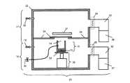
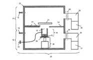
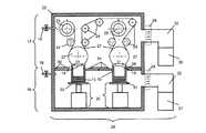
本発明の薄膜の製造方法は、図1に模式的に示すところの、以下の成膜装置を用いて実施することができる。図1(a)は成膜準備中の成膜装置を模式的に示す図、図1(b)は成膜中の成膜装置を模式的に示す図である。 The method for producing a thin film of the present invention can be carried out using the following film forming apparatus as schematically shown in FIG. FIG. 1A is a diagram schematically illustrating a film forming apparatus during film formation preparation, and FIG. 1B is a diagram schematically illustrating the film forming apparatus during film formation.
成膜装置20は真空槽22を含み、真空槽22は、成膜準備中、内部に蒸発源19が配置される蒸発室16と、蒸発室16に隣接して配置され、内部に基板21が配置される成膜室17とに区画される。蒸発室16及び成膜室17のそれぞれに、各室を真空排気するための真空ポンプ37,38が接続されている。蒸発室16及び成膜室17のそれぞれに、各室に非反応ガスを導入するための非反応ガス導入機構18が接続されている。蒸発室16の内部には、成膜材料15を保持し、開放面14を有する半密閉構造の、加熱可能な蒸発源19が配置されている。成膜室17の内部には、成膜対象物たる基板21が配置されている。蒸発源19は、移動機構35によって移動可能に配置されている。これによって、蒸発源19は、図1(b)に示すように開放面14を基板21に接近させることや、逆に図1(a)に示すように基板21から遠ざけることができる。蒸発室16と成膜室17との間にはコンダクタンス可変構造34が配置されており、これによって蒸発室16と成膜室17が区分けされている。コンダクタンス可変構造34を動かすことにより、成膜室16と蒸発室17との間の空間的連続性を完全に遮断若しくはほぼ遮断して両室の間に差圧を確保したり、又は、両室の空間を連続させて両室を同圧下に置くことができる。 The
蒸発室及び成膜室を構成する真空槽22は耐圧性の金属製容器であり、真空槽22と真空ポンプ37,38は真空バルブ(図示せず)を介して接続されている。真空ポンプ37,38には各種真空ポンプが適用可能であり、一般に、主ポンプと、油回転ポンプ等からなる補助ポンプとから構成される。主ポンプとしては、油拡散ポンプ、クライオポンプ、又は、ターボ分子ポンプを用いるのが好ましい。主ポンプの開閉を行う主バルブ32を設けることが望ましい。また、主ポンプと蒸発室及び成膜室との間に排気速度の調整を行うコンダクタンスバルブ29を設けることが望ましい。 The
非反応ガス導入機構18は、蒸発室16及び成膜室17に接続され、各室に非反応ガスを導入する。図1では蒸発室16及び成膜室17それぞれに非反応ガス導入機構18が接続されているが、これに限定されず、蒸発室16及び成膜室17のいずれか一方のみに非反応ガス導入機構18が接続されていてもよい。非反応ガス導入機構18は、例えば、ガスボンベ等からなるガス源(図示せず)、配管によってガス源と接続された流量コントローラ(図示せず)、真空槽と流量コントローラの間の配管、及び、ガス導入又はガス遮断を選択するためのガスバルブからなる。流量コントローラにはマスフローコントローラ等が用いられる。 The non-reactive
半密閉構造の蒸発源19は、内部に成膜材料15を収納し、蒸発材料の蒸散を可能にする開放面14を有する。蒸発源の形状は、例えば、上面に開口部を有する円柱形、又は、上面に開口部を有する直方体であってよい。蒸発源の上部に設けられた開口部を基板に近接させると、成膜材料の蒸気が周囲に飛散せず、基板21のみに堆積することになるので、成膜材料を効率良く利用できる。しかし、開口部が上方を向いていることは必ずしも必要でなく、例えば図6に示すように、側面に開口部を有する蒸発源を用いることも可能である。この時は、基板を垂直に配置すればよい。蒸発源を構成する材料としては、例えば、成膜材料との反応性の低い金属材料、炭素材料、又は、耐火物材料が用いられる。必要に応じてこれら材料の組合せによって蒸発源を構成することもできる。蒸発源19は、成膜準備段階では図1(a)に示すように全体が蒸発室16内に配置されているが、成膜時には図1(b)に示すように、少なくとも開放面14が成膜室17内部に突出して基板21と近接するような位置に配置される。 The
移動機構35は、図1に示すように、例えば蒸発源19を載せるステージ33を有する昇降機構である。昇降機構は、例えば、油圧シリンダ、ボールネジ、及び、ギアによって構成することができる。昇降機構によってステージを上下させることで、成膜源19の上部に設けた開放面14が、蒸発源の上方に配置された基板に接近又は後退することができる。移動機構はこれに限らず、例えば、開口部を側面に有する蒸発源を、水平方向に移動させる機構であってもよいし、垂直又は水平方向の直線運動に回転運動を組み合わせて開口部を基板に接近又は後退させる機構であってもよい。 As shown in FIG. 1, the moving
蒸発室16と成膜室17との境界にはコンダクタンス可変構造34が配置されている。コンダクタンス可変構造34を動作させることで、蒸発室16と成膜室17との間に差圧を確保したり、両室を同圧下に置いたりすることができる。コンダクタンス可変構造は例えば板状の可動隔壁であり、蒸発室16と成膜室17との連通路を完全に遮断若しくはほぼ遮断することで蒸発室と成膜室の間の連通状態を遮断し、両室間の差圧を確保することができる。これと共に、可動隔壁の一部又は全部を移動させることによって蒸発室と成膜室との連通路を形成することで両室の間の連通状態を拡大し、両室をほぼ同圧下に置くことができる。図3及び図4はコンダクタンス可変構造の動作例を模式的に示す。図3は可動隔壁がスライド方式のものを示し、図4は可動隔壁が両開き式のものを示す。図3及び図4において、(a)は連通路を遮断して差圧を確保している状態(差圧構造)、(b)は連通路を形成して前記差圧構造を解除している状態を示している。なお、蒸発源の加熱中に微量の蒸気が発生する場合、コンダクタンス可変構造を構成する部材によって防着を行うこともできるが、コンダクタンス可変構造と蒸発源との間に、軽度の防着用シャッター機構を別途設けてもよい。 A conductance
コンダクタンス可変構造が連通路を形成している状態(図3(b)及び図4(b))において、連通路の下方には、成膜源19の開放面14が配置され、その上方には、基板21が配置されている。成膜源19が移動機構35によって上方向に移動し、その開放面14が前記連通路を通過することで、開放面14を基板21に近接させることができる。従って、コンダクタンス可変構造が開くことによって形成される連通路は、成膜源19の開放面14を通過させる程度の大きさを有することが好ましい。 In the state where the conductance variable structure forms the communication path (FIGS. 3B and 4B), the
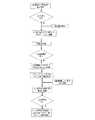
本発明の薄膜の製造方法は、以上説明した成膜装置内で薄膜を製造するものであり、以下の(a)〜(f)の工程を有する。
(a)前記成膜室と前記蒸発室を真空排気する第一工程。
(b)前記第一工程に次いで、前記コンダクタンス可変構造により前記蒸発室と前記成膜室との間で差圧が確保できる状態で、前記蒸発室に非反応ガスを導入して前記蒸発室内の圧力を所定圧力以上に調整し前記成膜材料の蒸発を抑制する第二工程。
(c)前記第一工程に次いで、前記コンダクタンス可変構造により前記蒸発室と前記成膜室との間で差圧が確保できる状態で、前記成膜室に非反応ガスを導入して前記成膜室内の圧力を前記所定圧力以上に調整する第三工程。
(d)第二工程及び第三工程の後、前記コンダクタンス可変構造を動作させ、前記蒸発室と前記成膜室との間で差圧が確保できる状態を解除する第四工程。
(e)第四工程の後、前記移動機構により前記蒸発源を移動させて前記開放面を前記基板に近接させる第五工程。
(f)第五工程の後、前記成膜室及び前記蒸発室内の前記圧力を前記所定圧力未満に低下させることにより、前記成膜材料の蒸発抑制を解除し前記基板上の成膜を開始する第六工程。The thin film manufacturing method of the present invention is a method for manufacturing a thin film in the film forming apparatus described above, and includes the following steps (a) to (f).
(A) A first step of evacuating the film formation chamber and the evaporation chamber.
(B) Subsequent to the first step, a non-reactive gas is introduced into the evaporation chamber in a state where a differential pressure can be secured between the evaporation chamber and the film forming chamber by the conductance variable structure. A second step in which the pressure is adjusted to a predetermined pressure or more to suppress evaporation of the film forming material;
(C) Subsequent to the first step, the film formation is performed by introducing a non-reactive gas into the film formation chamber in a state where a differential pressure can be secured between the evaporation chamber and the film formation chamber by the conductance variable structure. A third step of adjusting the pressure in the room to be equal to or higher than the predetermined pressure;
(D) A fourth step of operating the conductance variable structure after the second step and the third step to release a state in which a differential pressure can be secured between the evaporation chamber and the film formation chamber.
(E) A fifth step after the fourth step, in which the evaporation source is moved by the moving mechanism to bring the open surface close to the substrate.
(F) After the fifth step, by reducing the pressure in the film formation chamber and the evaporation chamber below the predetermined pressure, the evaporation suppression of the film formation material is released and film formation on the substrate is started. Sixth process.
図7は本発明の薄膜の製造方法のフローチャートを示す。 FIG. 7 shows a flowchart of the thin film manufacturing method of the present invention.
(a)の第一工程では、成膜装置内に基板及び成膜材料を所定の位置に配した後、蒸発室と成膜室の真空排気を行う。この工程では、蒸発室と成膜室を、蒸着に必要な程度まで高真空に排気することが望ましい。第一工程で予め高真空に排気しておくことによって、真空槽の内壁等の部材に付着している吸着ガス等を除去できるので、第六工程で成膜に適した高真空まで減圧する際に、当該高真空への到達が早くなる。高真空の程度は、成膜材料や要求される膜質によって異なるが、例えば0.01Pa以下、望ましくは0.001Pa以下である。この第一工程では、コンダクタンス可変構造34により連通路を遮断して成膜室と蒸発室の間に差圧が確保できる状態であってもよいし、両室を連続させた状態でもよい。この第一工程では、成膜材料は所定の蒸気圧を持つまでには至っていない。 In the first step (a), after the substrate and the film forming material are arranged in predetermined positions in the film forming apparatus, the evaporation chamber and the film forming chamber are evacuated. In this step, it is desirable to evacuate the evaporation chamber and the film formation chamber to a high vacuum to the extent necessary for vapor deposition. By evacuating to a high vacuum in the first step in advance, the adsorbed gas adhering to the members such as the inner wall of the vacuum chamber can be removed. In addition, the high vacuum is reached quickly. The degree of high vacuum varies depending on the film forming material and the required film quality, but is, for example, 0.01 Pa or less, preferably 0.001 Pa or less. In the first step, the conductance
第一工程に続く(b)の第二工程では、蒸発室と成膜室との間の連通路を完全に遮断又はほぼ遮断することで、蒸発室と成膜室との間で差圧が確保できる状態としている(図1(a))。 In the second step (b) following the first step, the communication path between the evaporation chamber and the film forming chamber is completely blocked or substantially blocked, so that the differential pressure between the evaporation chamber and the film forming chamber is reduced. The state can be secured (FIG. 1A).
蒸発室16内に設置されている蒸発源19には、例えば固体の成膜材料15が保持されており、この第二工程で成膜材料は加熱されることで、溶融し、やがて有意の蒸気圧(成膜に適した蒸気圧)を有するようになる。成膜材料の加熱方式としては、例えば抵抗加熱法又は誘導加熱法を用いることが好ましい。抵抗加熱の場合には、例えば蒸発源の周囲にヒーター線を巻き付けて蒸発源を加熱することができる。また、蒸発源の壁面に棒状ヒーターの差し込み口を設けておき、棒状ヒーターを用いて蒸発源を加熱することもできる。誘導加熱の場合、蒸発源の周囲にコイルが巻かれ、コイルに高周波電力を印加することで蒸発源が加熱される。 The
成膜材料の加熱により生じた成膜材料の蒸気圧に抗して、成膜材料の蒸発を抑制するために、差圧を確保できる状態で、蒸発室16に非反応ガスが導入される。この導入によって、前記蒸発室内の圧力を所定圧力以上に調整する。ここで、所定圧力以上に調整するとは、成膜材料が示す蒸気圧を超える圧力に調整することが好ましく、成膜材料が示す蒸気圧の2倍以上の圧力に調整することがより好ましい。蒸発室16での非反応ガスの圧力が成膜材料の蒸気圧を上回ることで、成膜材料の蒸発は抑制されることになる。この非反応ガス導入は、成膜材料の蒸発を確実に抑制するため、成膜材料の昇温と並行して行うことが好ましい。使用する非反応ガスの種類は、溶融した成膜材料との反応を回避する観点から適宜選択できるが、アルゴン又はネオンが望ましい。 In order to suppress evaporation of the film forming material against the vapor pressure of the film forming material generated by heating the film forming material, a non-reactive gas is introduced into the
成膜材料としては液体の成膜材料を用いることもできる。この場合、成膜材料を加熱しなくとも、蒸発室内の圧力低下により有意の蒸気圧を持つ場合があるので、第二工程で成膜材料の加熱は必ずしも必要ではない。しかし、成膜時に所望する蒸発速度に応じて、液体の成膜材料を適宜加熱してもよい。液体の成膜材料を用いる場合にも、成膜材料の有意の蒸気圧に抗するため非反応ガスを蒸発室16に導入する。いずれにしろ、第二工程では、非反応ガスを導入して蒸発室内の圧力を所定圧力以上とすることで、有意の蒸気圧を示す成膜材料の蒸発を抑制する。これにより、成膜開始前に成膜材料が蒸発飛散し、コンダクタンス可変構造等の部材に付着して材料ロスが生じるのを回避できる。 A liquid film forming material can also be used as the film forming material. In this case, even if the film forming material is not heated, the vapor deposition material may have a significant vapor pressure due to a pressure drop in the evaporation chamber. Therefore, it is not always necessary to heat the film forming material in the second step. However, the liquid film forming material may be appropriately heated in accordance with the desired evaporation rate during film formation. Even when a liquid film forming material is used, a non-reactive gas is introduced into the
次に説明する第三工程を実施する前に第二工程を実施する場合には、第二工程で蒸発室に非反応ガスを導入するのと並行して、成膜室では、第一工程から継続して真空排気を実施していることが好ましい。これによって、成膜室は高真空状態が維持され、内壁の吸着ガスは更に減少するので、プロセス全体における排気時間の短縮、及び、膜質の確保に有利である。 In the case where the second step is performed before the third step described below is performed, in the film formation chamber, in parallel with the introduction of the non-reactive gas into the evaporation chamber in the second step, It is preferable that evacuation is continuously performed. As a result, the film forming chamber is maintained in a high vacuum state, and the adsorbed gas on the inner wall is further reduced, which is advantageous in shortening the exhaust time in the entire process and ensuring the film quality.
第一工程に続く(c)の第三工程では、第二工程と同じく、蒸発室と成膜室との間の連通路を完全に遮断又はほぼ遮断することで、蒸発室と成膜室との間で差圧が確保できる状態としている(図1(a))。この状態で、成膜室にも非反応ガスを導入して、成膜室の圧力も、前述した所定圧力以上に調整する。成膜室と蒸発室との間に大きな圧力差が存在すると、成膜を開始する前に第四工程で差圧構造を解除する際に、蒸発室での急激な圧力低下、及び、蒸発源の温度変化が生じ、それによって成膜材料の飛散が生じることになる。本発明では、成膜室の圧力を、成膜材料が示す蒸気圧を超える圧力に予め調整しておくことで、第四工程での差圧構造解除時において、蒸発室での急激な圧力低下、及び、蒸発源の温度変化が生じるのを回避し、これによって成膜材料の不必要な飛散を防止する。 In the third step (c) subsequent to the first step, the communication path between the evaporation chamber and the film formation chamber is completely or substantially blocked, as in the second step, so that the evaporation chamber and the film formation chamber are separated. It is in a state where a differential pressure can be secured between them (FIG. 1A). In this state, a non-reactive gas is introduced also into the film forming chamber, and the pressure in the film forming chamber is adjusted to be equal to or higher than the predetermined pressure described above. If there is a large pressure difference between the film formation chamber and the evaporation chamber, when releasing the differential pressure structure in the fourth step before starting film formation, a sudden pressure drop in the evaporation chamber and the evaporation source This causes a change in temperature, which causes scattering of the film forming material. In the present invention, by adjusting the pressure in the film forming chamber to a pressure exceeding the vapor pressure indicated by the film forming material in advance, when the differential pressure structure is released in the fourth step, a rapid pressure drop in the evaporation chamber And avoiding the temperature change of the evaporation source, thereby preventing unnecessary scattering of the film forming material.
第三工程では、成膜室17の圧力を、第二工程で調整された蒸発室16の圧力とほぼ同じか、又は当該圧力よりも高くすることが望ましい。より望ましくは、蒸発室と成膜室の圧力をほぼ等しくする。これにより、差圧構造解除時の成膜材料の飛散を確実に防止することができる。 In the third step, it is desirable that the pressure in the
第二工程と第三工程の順序は限定されず、第二工程実施後に第三工程を実施してもよく、第三工程実施後に第二工程を実施してもよい。しかし、第二工程実施後に第三工程を実施することが、第二工程実施中に成膜室をより高真空にすることができ、また、非反応ガスの消費量を抑制できるので望ましい。第二工程実施後に第三工程を実施する場合には、第二工程で、蒸発源中の成膜材料が成膜に適した蒸気圧を持つようになった時点で、第三工程を開始することが望ましい。 The order of a 2nd process and a 3rd process is not limited, A 3rd process may be implemented after 2nd process implementation, and a 2nd process may be implemented after 3rd process implementation. However, it is desirable to perform the third step after the second step because the film forming chamber can be evacuated to a higher vacuum during the second step and the consumption of non-reactive gas can be suppressed. When the third step is performed after the second step, the third step is started when the film formation material in the evaporation source has a vapor pressure suitable for film formation in the second step. It is desirable.
第三工程での成膜室への非反応ガス導入は、成膜室に接続された非反応ガス導入機構を経由した導入であってもよいし、蒸発室を経由した導入であってもよい。後者の導入を採用する場合、成膜装置に、例えば、蒸発室と成膜室を接続する配管と、その配管経路に設置した開閉バルブとを設ければよい。この場合、例えば開閉バルブを閉じた状態で第二工程の蒸発室へのガス導入を行った後、開閉バルブを開くことにより、第三工程の成膜室へのガス導入を行うことができる。開閉バルブを開くことによる蒸発室の圧力低下を防ぐために、開閉バルブが開いている際には蒸発室に導入する非反応ガスの流量を増やすことが好ましい。同様に、第三工程実施後に第二工程を実施する場合には、第二工程での蒸発室への非反応ガス導入は、成膜室を経由した導入とすることができる。これらの場合には、蒸発室又は成膜室のいずれかに、非反応ガス導入機構が接続されていればよい。 The introduction of the non-reactive gas into the film formation chamber in the third step may be introduction via a non-reactive gas introduction mechanism connected to the film formation chamber, or introduction via an evaporation chamber. . When the latter introduction is employed, the film forming apparatus may be provided with, for example, a pipe connecting the evaporation chamber and the film forming chamber and an opening / closing valve installed in the pipe path. In this case, for example, the gas can be introduced into the film forming chamber in the third step by introducing the gas into the evaporation chamber in the second step with the on / off valve closed, and then opening the on / off valve. In order to prevent a pressure drop in the evaporation chamber due to the opening of the opening / closing valve, it is preferable to increase the flow rate of the non-reactive gas introduced into the evaporation chamber when the opening / closing valve is open. Similarly, when the second step is performed after the third step, the non-reactive gas can be introduced into the evaporation chamber in the second step through the film formation chamber. In these cases, a non-reactive gas introduction mechanism may be connected to either the evaporation chamber or the film formation chamber.
(d)の第四工程では、第二工程及び第三工程で設けていたコンダクタンス可変構造による差圧構造を解除する。差圧構造がコンダクタンス可変構造の一例である板状の可動隔壁によって達成されている場合、可動隔壁を移動させることによって蒸発室と成膜室の間の連通路を拡大することによって差圧構造を解除することができる。第四工程では、蒸発室と成膜室との間の差圧構造が解除されるが、成膜室と蒸発室双方の圧力が所定圧力以上であるので、急激な圧力変化や成膜材料の温度変化が生じるのを回避できる。第四工程においても、第二工程と同様、成膜材料は、有意の蒸気圧(成膜に適した蒸気圧)を有しながらも、非反応ガスによる圧力によって蒸発が抑制された状態にある。 In the fourth step (d), the differential pressure structure by the conductance variable structure provided in the second step and the third step is released. When the differential pressure structure is achieved by a plate-shaped movable partition that is an example of a conductance variable structure, the differential pressure structure is expanded by enlarging the communication path between the evaporation chamber and the film formation chamber by moving the movable partition. It can be canceled. In the fourth step, the differential pressure structure between the evaporation chamber and the film formation chamber is released, but since the pressure in both the film formation chamber and the evaporation chamber is equal to or higher than a predetermined pressure, sudden pressure changes and A temperature change can be avoided. Also in the fourth step, as in the second step, the film-forming material has a significant vapor pressure (vapor pressure suitable for film formation), but is in a state where evaporation is suppressed by the pressure of the non-reactive gas. .
第二工程〜第四工程では、蒸着源の開放面と基板は、その間にコンダクタンス可変構造が配されており、ある程度の距離を以て離れている。第四工程に続く(e)の第五工程では、移動機構を動作させることで蒸発源を移動させ、蒸発源の開放面を基板に近接させる。これによって、蒸着源と基板を、成膜に適した位置に配置する。この場合、蒸発源の上部を、蒸発室と成膜室との間の連通路(コンダクタンス可変構造が開くことによって形成された連通路)を通過させることによって、開放面と基板をより近づけることができる。 In the second step to the fourth step, the open surface of the vapor deposition source and the substrate are provided with a variable conductance structure therebetween, and are separated by a certain distance. In the fifth step (e) following the fourth step, the evaporation source is moved by operating the moving mechanism, and the open surface of the evaporation source is brought close to the substrate. Thus, the vapor deposition source and the substrate are arranged at positions suitable for film formation. In this case, the open surface and the substrate can be brought closer by allowing the upper part of the evaporation source to pass through the communication path between the evaporation chamber and the film forming chamber (the communication path formed by opening the conductance variable structure). it can.
蒸発源の移動は、例えば、油圧シリンダに接続されたステージを上昇させることによって、ステージ上に配置された蒸発源を上昇させ、蒸発源上部に設けられた開放面を、蒸発源上方に配置されている基板に近づけることによって行われる。第五工程によって、成膜に適した蒸気圧を有した成膜材料を保持した蒸発源を基板に近接させ、成膜準備を整えることができる。第五工程においても、真空槽内の圧力は所定圧力以上に保持されており、蒸発源内の成膜材料は、成膜に適した蒸気圧を有しながらも、その蒸発が抑制された状態にある。 The evaporation source is moved, for example, by raising the stage connected to the hydraulic cylinder to raise the evaporation source arranged on the stage, and the open surface provided above the evaporation source is arranged above the evaporation source. It is done by bringing it close to the substrate. By the fifth step, an evaporation source holding a film forming material having a vapor pressure suitable for film formation can be brought close to the substrate to prepare for film formation. Even in the fifth step, the pressure in the vacuum chamber is maintained at a predetermined pressure or higher, and the film-forming material in the evaporation source has a vapor pressure suitable for film formation, but its evaporation is suppressed. is there.
第五工程に続く(f)の第六工程では、真空槽内の圧力を前記所定圧力未満に低下させる。これにより、蒸発源内の成膜材料の蒸発抑制が解除され、基板への成膜が開始される。真空槽内の圧力低下は、成膜室と蒸発室への反応ガス導入量を低減したり、真空ポンプの排気速度を上げたりすることで達成できる。真空槽内の圧力が成膜材料の蒸気圧未満に低下することで、非反応ガスによる圧力によって蒸発が抑えられていた成膜材料が蒸発を始めることになり、これにより、基板上への成膜を開始することができる。 In the sixth step (f) following the fifth step, the pressure in the vacuum chamber is reduced below the predetermined pressure. Thereby, the suppression of evaporation of the film forming material in the evaporation source is released, and film formation on the substrate is started. The pressure drop in the vacuum chamber can be achieved by reducing the amount of reaction gas introduced into the film formation chamber and the evaporation chamber or by increasing the exhaust speed of the vacuum pump. When the pressure in the vacuum chamber drops below the vapor pressure of the film deposition material, the film deposition material that has been prevented from evaporating due to the pressure of the non-reactive gas begins to evaporate. The membrane can be started.
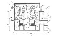
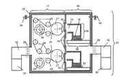
本発明の薄膜の製造方法は巻き取り式の成膜装置にも適用できる。巻き取り式成膜装置全体の構成の一例を、図2に模式的に示す。図1と同じ構成については説明を省略する。成膜室17の内部空間に、巻き芯ローラA23、複数の搬送ローラ24、キャン27、及び巻き芯ローラB26が収容され、蒸発室16の内部空間に、蒸発源19、移動機構35、及び成膜反応用ガス導入管30が収容されている。巻き芯ローラA23は、軸心回りに回転自在に設けられているローラ状部材であり、その表面に帯状で長尺の基板21が捲回され、最も近接する搬送ローラ24に向けて基板21を供給する。 The thin film manufacturing method of the present invention can also be applied to a roll-up film forming apparatus. An example of the configuration of the entire roll-up film forming apparatus is schematically shown in FIG. The description of the same configuration as in FIG. 1 is omitted. The
基板21には、各種高分子フィルム、各種金属箔、高分子フィルムと金属箔の複合体、又は、その他の上記材料に限定されない長尺基板を用いることができる。高分子フィルムとしては、例えば、ポリエチレンテレフタレート、ポリエチレンナフタレート、ポリアミド、ポリイミドが挙げられる。金属箔としては、例えば、アルミ箔、銅箔、ニッケル箔、チタニウム箔、ステンレス箔が挙げられる。基板の幅は例えば50〜1000mmであり、基板の望ましい厚みは例えば3〜150μmである。基板の幅が50mm未満では生産性に劣るが、本発明を適用できないということではない。基板の厚みが3μm未満では基板の熱容量が極めて小さいために基板に熱変形が発生しやすいが、本発明が適用不可であることを示すものではない。成膜中の基板の搬送速度は作成する薄膜の種類や成膜条件によって異なるが、例えば0.1〜500m/分である。搬送中の基板走行方向に印加される張力は、基板の材質若しくは厚み、又は成膜レートなどのプロセス条件によって適宜選択される。 As the
搬送ローラ24は軸心回りに回転自在に設けられているローラ状部材であり、巻き芯ローラA23から供給される基板21を成膜領域31に誘導し、最終的に巻き芯ローラB26に導く。成膜領域31を基板21がキャン27に沿って走行する際に、蒸発源から飛来した材料粒子が堆積し、基板21表面に薄膜が形成される。巻き芯ローラB26は、図示しない駆動手段によって回転駆動可能に設けられているローラ状部材であり、薄膜が形成された基板21を巻き取って保持する。 The
本発明の薄膜の製造方法に用いる成膜装置は、さらに、反応成膜用の成膜ガスを導入する手段を設けても良い。この成膜ガス導入手段としては、例えば、図1及び図2の成膜反応用ガス導入管30である。成膜反応用ガス導入管30は、例えば一端が蒸発源19の内部に導かれ、他端が真空槽22の外部に設けられる図示しない成膜反応用ガス供給手段に接続される管状部材である。成膜反応用ガス導入管30を通じて、成膜材料の蒸気に対し、例えば酸素、窒素等の成膜ガスを供給する。これによって、蒸発源から飛来した成膜材料の酸化物、窒化物又は酸窒化物を主成分とする薄膜が基板21表面に形成される。成膜反応用ガス供給手段には、ガスボンベ、ガス発生装置などがある。 The film forming apparatus used in the thin film manufacturing method of the present invention may further include means for introducing a film forming gas for reactive film formation. As this film forming gas introducing means, for example, the film forming reaction
基板21は、成膜領域31において、蒸発源から飛来した蒸気及び必要に応じて酸素、窒素などの成膜ガスの供給を受け、表面に薄膜が形成される。薄膜が形成された基板21は、別の搬送ローラ24を経由して巻き芯ローラB26に巻き取られる。 In the
以上のように、図2の成膜装置20によれば、巻き芯ローラA23から送り出された基板21が、搬送ローラ24を経由して走行し、巻き芯ローラB26に巻き取られる。その途上において、成膜領域31において、蒸発源から飛来した蒸気及び必要に応じて酸素、窒素の成膜ガスの供給を受けて基板上に薄膜が形成される。これらの動作によって、成膜装置20はノズル方式の蒸発源19を用いた巻き取り成膜を行うことができる。 As described above, according to the
図2の成膜装置20では、2つのキャン27及び2つの蒸発源19を設け、さらに2つのキャンの間に反転構造を設けている。これによって、基板の表面と裏面双方に薄膜を形成することを可能とする。しかし、本発明で使用できる巻き取り式成膜装置はこの態様に限定されず、1つのキャン27及び1つの蒸発源19を設けて基板の片面のみに薄膜を形成する装置であってもよい。 In the
(実施の形態1)
本発明の薄膜の製造方法の実施形態の一例を説明する。この実施形態では、シリコン薄膜からなるリチウムイオン二次電池用負極上にリチウム膜を形成する。以下に説明する各数値は一例にすぎず、本発明を限定するものではない。(Embodiment 1)
An example of an embodiment of the thin film manufacturing method of the present invention will be described. In this embodiment, a lithium film is formed on a negative electrode for a lithium ion secondary battery made of a silicon thin film. Each numerical value described below is only an example and does not limit the present invention.
古河サーキットフォイル(株)製の粗面化銅箔(厚さ18ミクロン、幅100mm)を集電体として用い、集電体の両面上にそれぞれシリコン多層薄膜を厚さ8μmに、真空蒸着法によって予め形成したものを、本発明の基板として用いる。 Using a roughened copper foil (
まず、前記シリコン多層薄膜を、巻き取り式の蒸着装置(図示しない)を用いて以下の手順で形成する。排気手段として口径14インチの油拡散ポンプを2台備えた、容積0.4立方メートルの真空槽を0.002パスカルまで排気した後に、成膜材料であるシリコンを溶解する。シリコンの溶解は日本電子(株)製の270度偏向型電子ビーム蒸発源を用いて行う。加速電圧−10kV、エミッション電流600mAの電子ビームを溶融シリコンに照射し、発生する蒸気を、キャンに沿って走行中の銅箔に差し向ける。集電体の搬送速度は1m/分、平均成膜速度は80nm/秒とする。 First, the said silicon multilayer thin film is formed in the following procedures using a winding type vapor deposition apparatus (not shown). After evacuating a vacuum chamber having a volume of 0.4 cubic meter and two oil diffusion pumps having a diameter of 14 inches as exhaust means to 0.002 Pascal, silicon as a film forming material is dissolved. Silicon is melted using a 270-degree deflection electron beam evaporation source manufactured by JEOL. The molten silicon is irradiated with an electron beam having an acceleration voltage of −10 kV and an emission current of 600 mA, and the generated vapor is directed along the can to the traveling copper foil. The current carrying speed of the current collector is 1 m / min, and the average film forming speed is 80 nm / second.
シリコン薄膜の成膜幅が85mmとなるように、メタルマスク(開口長は各100mm)を銅箔集電体に約2mmの距離で近接して設置する。銅箔集電体の搬送機構は往復走行が可能であり、一回の走行で集電体の両面に膜厚0.5ミクロン程度のシリコン薄膜が一層ずつ形成される。往復走行しながら成膜を16回繰り返すことによって、膜厚が約8ミクロンのシリコン多層薄膜を形成する。 A metal mask (with an opening length of 100 mm each) is placed close to the copper foil current collector at a distance of about 2 mm so that the silicon thin film has a width of 85 mm. The transport mechanism of the copper foil current collector can reciprocate, and a silicon thin film having a film thickness of about 0.5 microns is formed on both sides of the current collector by one run. By repeating the
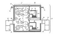
次に、シリコン薄膜が形成された集電体を基板として、本発明の薄膜の製造方法により、基板の両面にリチウム膜を形成する。図5(1)〜(6)は、この実施形態1を工程を追って示す図である。図5において、図2と同じ構成要素については同じ符号を用い、説明を省略する。なおリチウムの融点は180℃である。 Next, using the current collector on which the silicon thin film is formed as a substrate, lithium films are formed on both surfaces of the substrate by the thin film manufacturing method of the present invention. 5 (1) to (6) are diagrams showing the first embodiment step by step. In FIG. 5, the same components as those in FIG. The melting point of lithium is 180 ° C.
(第一の工程)
図5(1)で示すとおり、シリコン薄膜が予め形成されている基板21を巻き芯ローラA23に取付け、巻き芯ローラA23から搬送ローラ24、キャン27を経て巻き芯ローラB26に至る搬送経路に巡らせる。その後、真空粗引きを経て、蒸発室及び成膜室を14インチの油拡散ポンプ37,38によって高真空排気する。この時コンダクタンス可変構造34は、蒸発室16と成膜室17間のコンダクタンスが最大になるような連通の状態(差圧構造解除)とする。蒸発源19の上部には開放面14を設け、当該開放面は、キャン上の基板と近接できるよう、キャンの形状に合わせて湾曲させている。蒸発源は、ステンレス鋼壁面とヒーター加熱源を備えたノズル方式の蒸発源であり、その内部空間に20gの金属リチウムを収納している。移動機構を用いて蒸発源は下降させておき、基板から最も遠い位置に配置しておく。この状態で、30分間程度の真空排気を行い、蒸発室及び成膜室の圧力を0.005Paに調節する。(First step)
As shown in FIG. 5A, the
(第二の工程)
第一工程で蒸発室の圧力が0.005Paとなった時点で、図5(2)で示すとおり、コンダクタンス可変構造を動作させ、蒸発室16と成膜室17間のコンダクタンスが最小になるように、両室間の連通をほぼ遮断する。この状態で蒸発室及び成膜室共に真空排気を続行すると共に、蒸発室に50sccmのアルゴン(非反応ガス)を導入する。これにより蒸発室の圧力を約0.05Paに調整する。目標温度を480℃としてノズル方式蒸発源の加熱を開始し、蒸発源の温度が300℃となったところで蒸発室へのアルゴン導入量を100sccmに増加すると共に、蒸発室と主バルブの間のコンダクタンスバルブ29を半閉状態にして、主ポンプへの負荷が過大にならないようにしつつ蒸発室の圧力を0.2Paまで上昇させる。この蒸発室の圧力により、加熱により溶融し蒸気圧を持ち始めたリチウムの蒸発が抑制される。(Second step)
When the pressure in the evaporation chamber reaches 0.005 Pa in the first step, as shown in FIG. 5B, the conductance variable structure is operated so that the conductance between the
(第三の工程)
図5(3)で示すように、コンダクタンス可変構造の状態は維持したまま、蒸発源の温度が目標温度の480℃で安定した時点で成膜室へのアルゴン導入を開始する。成膜室にも100sccmでアルゴンを導入し、成膜室と主バルブの間のコンダクタンスバルブの開度を調整して成膜室の圧力を0.2Paまで上昇させる。(Third process)
As shown in FIG. 5 (3), the introduction of argon into the film formation chamber is started when the temperature of the evaporation source is stabilized at the target temperature of 480 ° C. while the state of the variable conductance structure is maintained. Argon is also introduced into the film forming chamber at 100 sccm, and the opening of the conductance valve between the film forming chamber and the main valve is adjusted to increase the pressure in the film forming chamber to 0.2 Pa.
(第四の工程)
図5(4)で示すように、コンダクタンス可変構造の可動隔壁を移動し、蒸発室と成膜室間のコンダクタンスが最大になるような連通の状態にする。成膜室、蒸発室共に圧力は0.2Paを維持する。(Fourth process)
As shown in FIG. 5 (4), the movable partition wall having a variable conductance structure is moved so that the conductance between the evaporation chamber and the film forming chamber is maximized. The pressure is maintained at 0.2 Pa in both the film formation chamber and the evaporation chamber.
(第五の工程)
成膜室及び蒸発室の圧力を維持したまま、図5(5)で示すように、移動機構により蒸発源の位置を上昇させ、蒸発源の開放面を基板に近接させる。これにより、キャンと蒸発源の開放面との距離を3mm程度とする。また、基板の巻き取り走行を速度2m/minで開始する。(Fifth process)
While maintaining the pressures in the film formation chamber and the evaporation chamber, as shown in FIG. 5 (5), the position of the evaporation source is raised by the moving mechanism, and the open surface of the evaporation source is brought close to the substrate. Thereby, the distance between the can and the open surface of the evaporation source is set to about 3 mm. Further, the substrate winding is started at a speed of 2 m / min.
(第六の工程)
図5(6)で示すように、蒸発室及び成膜室共に、コンダクタンスバルブを全開とするとともに、非反応ガスの導入を停止することで、蒸発室及び成膜室の圧力を0.005Paまで低下させる。これによってリチウムの蒸発抑制が解除され、リチウムが蒸発して基板に付着し、膜厚1.5ミクロン相当のリチウム膜が基板上に形成される。リチウム膜は、成膜後直ちにシリコン薄膜中に反応吸収される。(Sixth process)
As shown in FIG. 5 (6), both the evaporation chamber and the film formation chamber are fully opened, and the introduction of the non-reactive gas is stopped, whereby the pressure in the evaporation chamber and the film formation chamber is reduced to 0.005 Pa. Reduce. As a result, the suppression of the evaporation of lithium is released, the lithium is evaporated and adheres to the substrate, and a lithium film having a thickness of 1.5 microns is formed on the substrate. The lithium film is absorbed and reacted into the silicon thin film immediately after the film formation.
(実施の形態2)
本発明の薄膜の製造方法の実施形態の別の一例を説明する。この実施形態では、シリコン酸化物薄膜からなるリチウムイオン二次電池用負極上にリチウム膜を形成する。以下に説明する各数値は一例にすぎず、本発明を限定するものではない。(Embodiment 2)
Another example of the embodiment of the thin film manufacturing method of the present invention will be described. In this embodiment, a lithium film is formed on a negative electrode for a lithium ion secondary battery made of a silicon oxide thin film. Each numerical value described below is only an example and does not limit the present invention.
古河サーキットフォイル(株)製の粗面化銅箔(厚さ18ミクロン、幅100mm)を集電体として用い、集電体の両面上にそれぞれシリコン酸化物多層薄膜を厚さ15μmに、真空蒸着法によって予め形成したものを、本発明の基板として用いる。 Using roughened copper foil (
まず、前記シリコン酸化物多層薄膜を、巻き取り式の蒸着装置(図示しない)を用いて以下の手順で形成する。排気手段として口径14インチの油拡散ポンプを2台備えた、容積0.4立方メートルの真空槽を0.002パスカルまで排気した後に、成膜材料であるシリコンを溶解する。シリコンの溶解は日本電子(株)製の270度偏向型電子ビーム蒸発源を用いて行う。加速電圧−10kV、エミッション電流950mAの電子ビームを溶融シリコンに照射し、発生する蒸気を、キャンに沿って走行中の銅箔に差し向ける。集電体の搬送速度は1m/分、平均成膜速度は160nm/秒とする。 First, the said silicon oxide multilayer thin film is formed in the following procedures using a winding type vapor deposition apparatus (not shown). After evacuating a vacuum chamber having a volume of 0.4 cubic meter and two oil diffusion pumps having a diameter of 14 inches as exhaust means to 0.002 Pascal, silicon as a film forming material is dissolved. Silicon is melted using a 270-degree deflection electron beam evaporation source manufactured by JEOL. An electron beam with an acceleration voltage of −10 kV and an emission current of 950 mA is irradiated onto the molten silicon, and the generated vapor is directed along the can to the copper foil that is running. The current carrying speed of the current collector is 1 m / min, and the average film forming speed is 160 nm / sec.
シリコン薄膜の成膜幅が85mmとなるように、メタルマスク(開口長は各100mm)を銅箔基板に約2mmの距離で近接して設置する。また、銅箔集電体の成膜面側に設置した反応ガスノズルからメタルマスクの開口部に酸素ガスを60sccm差し向ける。これによって銅箔基板上にシリコン酸化物薄膜が形成される。銅箔集電体の搬送機構は往復走行が可能であり、一回の走行で集電体の両面に膜厚1ミクロン程度のシリコン薄膜が一層ずつ形成される。往復走行しながら成膜を15回繰り返すことによって、膜厚が約15ミクロンのシリコン酸化物多層薄膜を形成する。 A metal mask (opening length is 100 mm each) is placed close to the copper foil substrate at a distance of about 2 mm so that the silicon thin film has a width of 85 mm. In addition, oxygen gas is directed at 60 sccm from the reaction gas nozzle installed on the film forming surface side of the copper foil current collector to the opening of the metal mask. As a result, a silicon oxide thin film is formed on the copper foil substrate. The transport mechanism of the copper foil current collector can reciprocate, and a silicon thin film having a film thickness of about 1 micron is formed on both sides of the current collector by one run. By repeating the
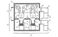
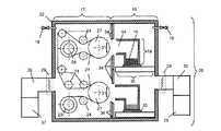
次に、シリコン酸化物薄膜が形成された集電体を基板として、本発明の薄膜の製造方法により、基板の両面にリチウム膜を形成する。図6(1)〜(6)は、この実施形態2を工程を追って示す図である。図6において、図2と同じ構成要素については同じ符号を用い、説明を省略する。図6では、成膜室と蒸発室は水平方向に並列しており、蒸発源19は側面に開放面を有する。移動機構は蒸発源19を水平方向に移動させる。 Next, using the current collector on which the silicon oxide thin film is formed as a substrate, lithium films are formed on both surfaces of the substrate by the thin film manufacturing method of the present invention. 6 (1) to 6 (6) are diagrams showing the second embodiment step by step. In FIG. 6, the same components as those in FIG. In FIG. 6, the film formation chamber and the evaporation chamber are arranged in parallel in the horizontal direction, and the
(第一の工程)
図6(1)で示すとおり、シリコン酸化物薄膜が予め形成されている基板21を巻き芯ローラA23に取付け、巻き芯ローラA23から搬送ローラ24、キャン27を経て巻き芯ローラB26に至る搬送経路に巡らせる。その後、真空粗引きを経て、蒸発室及び成膜室を14インチの油拡散ポンプ37,38によって高真空排気する。この時コンダクタンス可変構造34は、蒸発室16と成膜室17間のコンダクタンスが最小になるようほぼ遮断の状態(差圧構造)とする。蒸発源19の上部には開放面14を設け、当該開放面は、キャン上の基板と近接できるよう、キャンの形状に合わせて湾曲させている。蒸発源は、ステンレス鋼壁面とヒーター加熱源を備えたノズル方式の蒸発源であり、その内部空間に20gの金属リチウムを収納している。移動機構を用いて蒸発源は図6中の右側に移動させておき、基板から最も遠い位置に配置しておく。この状態で、30分間程度の真空排気を行い、蒸発室及び成膜室の圧力を0.005Paに調節する。(First step)
As shown in FIG. 6 (1), a
(第二の工程)
第一工程で蒸発室の圧力が0.005Paとなった時点で、図6(2)で示すとおり、差圧構造を維持し、蒸発室及び成膜室共に真空排気を続行するとともに、蒸発室に50sccmのアルゴン(非反応ガス)を導入する。これにより、蒸発室の圧力を約0.05Paに調整する。目標温度を500℃としてノズル方式蒸発源の加熱を開始し、蒸発源の温度が300℃となったところで蒸発室へのアルゴン導入量を100sccmに増加すると共に、蒸発室と主バルブの間のコンダクタンスバルブ29を半閉状態にして、主ポンプへの負荷が過大にならないようにしつつ蒸発室の圧力を0.2Paまで上昇させる。更に、蒸発源の温度が450℃となったところで蒸発室へのアルゴン導入量を150sccmにさらに増加すると共に、蒸発室と主バルブの間のコンダクタンスバルブ29を調整して蒸発室の圧力を0.4Paまで上昇させる。この蒸発室の圧力により、加熱により溶融し蒸気圧を持ち始めたリチウムの蒸発が抑制される。(Second step)
When the pressure in the evaporation chamber reaches 0.005 Pa in the first step, as shown in FIG. 6 (2), the differential pressure structure is maintained, and both the evaporation chamber and the film formation chamber are continuously evacuated, and the evaporation chamber 50 sccm of argon (non-reactive gas) is introduced. Thereby, the pressure of the evaporation chamber is adjusted to about 0.05 Pa. Heating of the nozzle-type evaporation source is started at a target temperature of 500 ° C. When the temperature of the evaporation source reaches 300 ° C., the amount of argon introduced into the evaporation chamber is increased to 100 sccm, and the conductance between the evaporation chamber and the main valve is increased. The
(第三の工程)
図6(3)で示すように、コンダクタンス可変構造の状態は維持したまま、蒸発源の温度が目標温度の500℃で安定した時点で成膜室へのアルゴン導入を開始する。成膜室にも150sccmでアルゴンを導入し、成膜室と主バルブの間のコンダクタンスバルブの開度を調整して成膜室の圧力を0.4Paまで上昇させる。(Third process)
As shown in FIG. 6 (3), introduction of argon into the film formation chamber is started when the temperature of the evaporation source is stabilized at the target temperature of 500 ° C. while maintaining the state of the conductance variable structure. Argon is also introduced into the film forming chamber at 150 sccm, and the opening of the conductance valve between the film forming chamber and the main valve is adjusted to increase the pressure in the film forming chamber to 0.4 Pa.
(第四の工程)
図6(4)で示すように、コンダクタンス可変構造の可動隔壁を移動し、蒸発室と成膜室間のコンダクタンスが最大になるような連通の状態にする。成膜室、蒸発室共に圧力は0.4Paを維持する。(Fourth process)
As shown in FIG. 6 (4), the movable partition wall having a variable conductance structure is moved so that the conductance between the evaporation chamber and the film forming chamber is maximized. The pressure is maintained at 0.4 Pa in both the film formation chamber and the evaporation chamber.
(第五の工程)
成膜室及び蒸発室の圧力を維持したまま、図6(5)で示すように、移動機構により蒸発源を左側に移動させ、蒸発源の開放面を基板に近接させる。これにより、キャンと蒸発源の開放面との距離を3mm程度とする。また、基板の巻き取り走行を速度1m/minで開始する。(Fifth process)
While maintaining the pressure in the film formation chamber and the evaporation chamber, as shown in FIG. 6 (5), the evaporation source is moved to the left by the moving mechanism, and the open surface of the evaporation source is brought close to the substrate. Thereby, the distance between the can and the open surface of the evaporation source is set to about 3 mm. Further, the winding operation of the substrate is started at a speed of 1 m / min.
(第六の工程)
図6(6)で示すように、蒸発室及び成膜室共に、コンダクタンスバルブを全開とするとともに、非反応ガスの導入を停止することで、蒸発室及び成膜室の圧力を0.005Paまで低下させる。これによってリチウムの蒸発抑制が解除され、リチウムが蒸発して基板に付着し、膜厚6ミクロン相当のリチウム膜が基板上に形成される。リチウム膜は、成膜後直ちにシリコン酸化物薄膜中に反応吸収される。(Sixth process)
As shown in FIG. 6 (6), both the evaporation chamber and the film formation chamber are fully opened, and the introduction of the non-reactive gas is stopped, whereby the pressure in the evaporation chamber and the film formation chamber is reduced to 0.005 Pa. Reduce. As a result, the suppression of the evaporation of lithium is released, the lithium is evaporated and adheres to the substrate, and a lithium film having a thickness of 6 microns is formed on the substrate. The lithium film is absorbed into the silicon oxide thin film immediately after film formation.
以上、発明を実施するための形態を具体的に述べたが、本発明はこれらに限定されるものではない。成膜材料としては、各種金属や、加熱蒸発可能な有機材料など、リチウム以外の各種成膜材料を用いることができる。その際、所望の蒸気圧が達成される温度において当該成膜材料と蒸発源構成材が溶融や合金化等の反応をしないように、蒸発源の構成材料を適宜選ぶことができる。 As mentioned above, although the form for inventing was described concretely, this invention is not limited to these. As the film forming material, various film forming materials other than lithium, such as various metals and organic materials that can be heated and evaporated, can be used. At that time, the constituent material of the evaporation source can be appropriately selected so that the film forming material and the evaporation source constituent material do not react such as melting or alloying at a temperature at which a desired vapor pressure is achieved.
以上では、具体的な適用例として、リチウムイオン二次電池用負極を形成する場合について説明したが、本発明はこれに限定されるものではない。本発明によれば、例えば、電気化学キャパシタ用の極板を形成することもできる。また、有機物薄膜、装飾フィルム、太陽電池、ガスバリア膜、各種センサ、各種光学膜等をはじめとする、高効率安定成膜が要求される様々な用途に適用することができる。さらに、各種デバイスの形成を行う際の薄膜の製造方法にも応用することができる。 Although the case where the negative electrode for lithium ion secondary batteries is formed as a specific application example has been described above, the present invention is not limited to this. According to the present invention, for example, an electrode plate for an electrochemical capacitor can be formed. Moreover, it can be applied to various uses that require highly efficient and stable film formation, such as organic thin films, decorative films, solar cells, gas barrier films, various sensors, and various optical films. Further, the present invention can be applied to a method for manufacturing a thin film when various devices are formed.
本発明に係る薄膜の製造方法は、ノズル方式の蒸発源を用いた成膜において、成膜前に必要な真空排気時間を短縮し、膜質を高め、材料利用効率を高め、材料飛散による真空槽の汚染を防止することができる。また、各種基板搬送系と組み合わせることもできるので、高効率で安定した成膜を達成する薄膜の製造方法を実現することができる。 The method for producing a thin film according to the present invention is a vacuum chamber that uses a nozzle-type evaporation source to shorten the evacuation time required before film formation, improve film quality, increase material utilization efficiency, and material scattering. Contamination can be prevented. In addition, since it can be combined with various substrate transport systems, a thin film manufacturing method that achieves highly efficient and stable film formation can be realized.
14 開放面
15 成膜材料
16 蒸発室
17 成膜室
18 非反応ガス導入機構
19 蒸発源
20 成膜装置
21 基板
22 真空槽
23 巻き芯ローラA
24 搬送ローラ
26 巻き芯ローラB
27 キャン
29 コンダクタンスバルブ
30 成膜反応用ガス導入管
31 成膜領域
32 主バルブ
33 ステージ
34 コンダクタンス可変構造
35 移動機構
37 真空ポンプ
38 真空ポンプDESCRIPTION OF
24 Conveying
27 Can 29
Claims (5)
Translated fromJapanese前記成膜装置は、
蒸発室と、
前記蒸発室に隣接して配置され、内部に基板を配置する成膜室と、
前記蒸発室及び前記成膜室のそれぞれに接続された真空ポンプと、
前記蒸発室及び前記成膜室のうち一方又は双方に接続された非反応ガス導入機構と、
前記蒸発室内に配置され、成膜材料を保持し、開放面を有する半密閉構造の蒸発源と、
前記開放面を前記基板に近接させることができるよう前記蒸発源を移動させる移動機構と、
前記蒸発室と前記成膜室との間に配置されたコンダクタンス可変構造と、を含み、
前記方法は、
前記成膜室と前記蒸発室を真空排気する第一工程と、
前記第一工程に次いで、前記コンダクタンス可変構造により前記蒸発室と前記成膜室との間で差圧が確保できる状態で、前記蒸発室に非反応ガスを導入して前記蒸発室内の圧力を所定圧力以上に調整し前記成膜材料の蒸発を抑制する第二工程と、
前記第一工程に次いで、前記コンダクタンス可変構造により前記蒸発室と前記成膜室との間で差圧が確保できる状態で、前記成膜室に非反応ガスを導入して前記成膜室内の圧力を前記所定圧力以上に調整する第三工程と、
第二工程及び第三工程の後、前記コンダクタンス可変構造を動作させ、前記蒸発室と前記成膜室との間で差圧が確保できる状態を解除する第四工程と、
第四工程の後、前記移動機構により前記蒸発源を移動させて前記開放面が少なくとも前記成膜室内部に突出するまで前記蒸発源を前記基板に近接させる第五工程と、
第五工程の後、前記成膜室及び前記蒸発室内の前記圧力を前記所定圧力未満に低下させることにより、前記成膜材料の蒸発抑制を解除し前記基板上の成膜を開始する第六工程と、
を含む、薄膜の製造方法。A method of manufacturing a thin film in a film forming apparatus,
The film forming apparatus includes:
An evaporation chamber,
A film forming chamber disposed adjacent to the evaporation chamber and having a substrate disposed therein;
A vacuum pump connected to each of the evaporation chamber and the film formation chamber;
A non-reactive gas introduction mechanism connected to one or both of the evaporation chamber and the film formation chamber;
A semi-enclosed evaporation source that is disposed in the evaporation chamber, holds a film forming material, and has an open surface;
A moving mechanism for moving the evaporation source so that the open surface can be brought close to the substrate;
A conductance variable structure disposed between the evaporation chamber and the film formation chamber,
The method
A first step of evacuating the film formation chamber and the evaporation chamber;
Subsequent to the first step, a non-reactive gas is introduced into the evaporation chamber so that a pressure difference between the evaporation chamber and the film forming chamber can be secured by the conductance variable structure, and the pressure in the evaporation chamber is set to a predetermined value. A second step of adjusting the pressure above the pressure to suppress evaporation of the film-forming material;
Following the first step, a non-reactive gas is introduced into the film formation chamber in a state in which a differential pressure can be secured between the evaporation chamber and the film formation chamber by the conductance variable structure. A third step of adjusting the pressure above the predetermined pressure;
A fourth step of operating the conductance variable structure after the second step and the third step to release a state in which a differential pressure can be secured between the evaporation chamber and the film formation chamber;
After the fourth step, a fifth step of moving the evaporation source by the moving mechanism to bring theevaporation source close to the substrateuntil the open surfaceprotrudes at least into the film formation chamber ;
After the fifth step, the sixth step of releasing the suppression of evaporation of the film forming material and starting the film formation on the substrate by lowering the pressure in the film forming chamber and the evaporation chamber below the predetermined pressure. When,
A method for producing a thin film.
Priority Applications (1)
| Application Number | Priority Date | Filing Date | Title |
|---|---|---|---|
| JP2012520270AJP5807217B2 (en) | 2010-06-16 | 2011-06-01 | Thin film manufacturing method |
Applications Claiming Priority (4)
| Application Number | Priority Date | Filing Date | Title |
|---|---|---|---|
| JP2010137224 | 2010-06-16 | ||
| JP2010137224 | 2010-06-16 | ||
| PCT/JP2011/003084WO2011158453A1 (en) | 2010-06-16 | 2011-06-01 | Method for manufacturing thin film |
| JP2012520270AJP5807217B2 (en) | 2010-06-16 | 2011-06-01 | Thin film manufacturing method |
Publications (2)
| Publication Number | Publication Date |
|---|---|
| JPWO2011158453A1 JPWO2011158453A1 (en) | 2013-08-19 |
| JP5807217B2true JP5807217B2 (en) | 2015-11-10 |
Family
ID=45347869
Family Applications (1)
| Application Number | Title | Priority Date | Filing Date |
|---|---|---|---|
| JP2012520270AExpired - Fee RelatedJP5807217B2 (en) | 2010-06-16 | 2011-06-01 | Thin film manufacturing method |
Country Status (4)
| Country | Link |
|---|---|
| US (1) | US8877291B2 (en) |
| JP (1) | JP5807217B2 (en) |
| CN (1) | CN102482763B (en) |
| WO (1) | WO2011158453A1 (en) |
Families Citing this family (13)
| Publication number | Priority date | Publication date | Assignee | Title |
|---|---|---|---|---|
| DE102012014915B4 (en)* | 2012-07-29 | 2021-11-18 | Hochschule München | Method for depositing a vapor deposition material on a substrate via a pressure-controlled deposition rate |
| US10569291B2 (en)* | 2014-05-23 | 2020-02-25 | Shincron Co., Ltd. | Film formation method and film formation apparatus for thin film |
| US9885110B2 (en)* | 2014-08-06 | 2018-02-06 | United Technologies Corporation | Pressure modulated coating |
| TWI582251B (en)* | 2014-10-31 | 2017-05-11 | 財團法人工業技術研究院 | Evaporation system and evaporation method |
| CN104789930B (en)* | 2015-04-24 | 2016-05-11 | 京东方科技集团股份有限公司 | Evaporated device and adopt the method for operating of this evaporated device |
| JP6608615B2 (en)* | 2015-05-18 | 2019-11-20 | 株式会社アルバック | Positive electrode active material film and film forming method |
| WO2020230359A1 (en)* | 2019-05-13 | 2020-11-19 | 株式会社アルバック | Deposition unit, and vacuum deposition device provided with said deposition unit |
| JP6713093B1 (en)* | 2019-05-13 | 2020-06-24 | 株式会社アルバック | Vapor deposition unit and vacuum vapor deposition apparatus including the vapor deposition unit |
| WO2021074952A1 (en)* | 2019-10-15 | 2021-04-22 | 学校法人東海大学 | Vacuum deposition method and vacuum deposition device |
| CN111139447B (en)* | 2020-02-25 | 2023-11-03 | 费勉仪器科技(上海)有限公司 | Device for realizing ultrahigh vacuum evaporation by utilizing differential air extraction system |
| JP7653862B2 (en)* | 2021-08-11 | 2025-03-31 | 信越化学工業株式会社 | Negative electrode |
| CN115110040B (en)* | 2022-06-20 | 2024-05-14 | 北京维开科技有限公司 | Independent double-chamber electron beam evaporation coating equipment |
| JP2024068531A (en)* | 2022-11-08 | 2024-05-20 | キヤノントッキ株式会社 | Film forming apparatus, film forming method, and electronic device manufacturing method |
Citations (5)
| Publication number | Priority date | Publication date | Assignee | Title |
|---|---|---|---|---|
| JPS61240436A (en)* | 1985-04-18 | 1986-10-25 | Matsushita Electric Ind Co Ltd | Production of magnetic recording medium |
| JPH0931633A (en)* | 1995-07-20 | 1997-02-04 | Fujitsu General Ltd | Optical thin film forming equipment |
| JPH10158820A (en)* | 1996-12-06 | 1998-06-16 | Ulvac Japan Ltd | Vapor deposition device, organic vaporization source and production of organic thin film |
| JP2003129224A (en)* | 2001-10-26 | 2003-05-08 | Matsushita Electric Works Ltd | Apparatus and process for vacuum deposition |
| JP2009062566A (en)* | 2007-09-05 | 2009-03-26 | Sony Corp | Evaporation apparatus, and method of manufacturing anode and battery using the same |
Family Cites Families (10)
| Publication number | Priority date | Publication date | Assignee | Title |
|---|---|---|---|---|
| JP3231373B2 (en) | 1991-12-20 | 2001-11-19 | 松下電器産業株式会社 | Apparatus and method for forming synthetic resin film |
| US5803976A (en)* | 1993-11-09 | 1998-09-08 | Imperial Chemical Industries Plc | Vacuum web coating |
| GB9323034D0 (en)* | 1993-11-09 | 1994-01-05 | Gen Vacuum Equip Ltd | Vacuum web coating |
| JP2942239B2 (en) | 1997-05-23 | 1999-08-30 | キヤノン株式会社 | Exhaust method and exhaust apparatus, plasma processing method and plasma processing apparatus using the same |
| EP0962260B1 (en)* | 1998-05-28 | 2005-01-05 | Ulvac, Inc. | Material evaporation system |
| US6275649B1 (en)* | 1998-06-01 | 2001-08-14 | Nihon Shinku Gijutsu Kabushiki Kaisha | Evaporation apparatus |
| US6641674B2 (en)* | 2000-11-10 | 2003-11-04 | Helix Technology Inc. | Movable evaporation device |
| JP4906018B2 (en)* | 2001-03-12 | 2012-03-28 | 株式会社半導体エネルギー研究所 | Film forming method, light emitting device manufacturing method, and film forming apparatus |
| JP4844867B2 (en)* | 2005-11-15 | 2011-12-28 | 住友電気工業株式会社 | Method of operating vacuum deposition apparatus and vacuum deposition apparatus |
| JP2009152189A (en) | 2007-11-29 | 2009-07-09 | Panasonic Corp | Method for producing negative electrode for nonaqueous electrolyte secondary battery, negative electrode for nonaqueous electrolyte secondary battery, and nonaqueous electrolyte secondary battery |
- 2011
- 2011-06-01JPJP2012520270Apatent/JP5807217B2/ennot_activeExpired - Fee Related
- 2011-06-01WOPCT/JP2011/003084patent/WO2011158453A1/enactiveApplication Filing
- 2011-06-01USUS13/390,633patent/US8877291B2/ennot_activeExpired - Fee Related
- 2011-06-01CNCN201180003595.0Apatent/CN102482763B/ennot_activeExpired - Fee Related
Patent Citations (5)
| Publication number | Priority date | Publication date | Assignee | Title |
|---|---|---|---|---|
| JPS61240436A (en)* | 1985-04-18 | 1986-10-25 | Matsushita Electric Ind Co Ltd | Production of magnetic recording medium |
| JPH0931633A (en)* | 1995-07-20 | 1997-02-04 | Fujitsu General Ltd | Optical thin film forming equipment |
| JPH10158820A (en)* | 1996-12-06 | 1998-06-16 | Ulvac Japan Ltd | Vapor deposition device, organic vaporization source and production of organic thin film |
| JP2003129224A (en)* | 2001-10-26 | 2003-05-08 | Matsushita Electric Works Ltd | Apparatus and process for vacuum deposition |
| JP2009062566A (en)* | 2007-09-05 | 2009-03-26 | Sony Corp | Evaporation apparatus, and method of manufacturing anode and battery using the same |
Also Published As
| Publication number | Publication date |
|---|---|
| US20120141677A1 (en) | 2012-06-07 |
| CN102482763B (en) | 2015-04-08 |
| WO2011158453A1 (en) | 2011-12-22 |
| CN102482763A (en) | 2012-05-30 |
| US8877291B2 (en) | 2014-11-04 |
| JPWO2011158453A1 (en) | 2013-08-19 |
Similar Documents
| Publication | Publication Date | Title |
|---|---|---|
| JP5807217B2 (en) | Thin film manufacturing method | |
| JP5807216B2 (en) | Thin film manufacturing method | |
| US11680322B2 (en) | Method for forming a laminated film on a substrate | |
| US20100272901A1 (en) | Thin film forming apparatus and thin film forming method | |
| JP4562811B2 (en) | Thin film formation method | |
| JP6513221B2 (en) | Method and coating equipment | |
| JP5058396B1 (en) | Thin film manufacturing method and manufacturing apparatus | |
| WO2011093073A1 (en) | Thin film production device, thin film production method, and substrate conveying rollers | |
| JPWO2008111306A1 (en) | Vapor deposition apparatus and film manufacturing method using vapor deposition apparatus | |
| JPWO2018193993A1 (en) | Film forming apparatus and film forming method | |
| WO2019156005A1 (en) | Thin film formation method, thin film formation device, and lithium battery | |
| CN104364415A (en) | Method for producing transparent gas-barrier film, device for producing transparent gas-barrier film, and organic electroluminescence device | |
| US20250059639A1 (en) | Apparatus for providing a liquefied material, dosage system and method for dosing a liquefied material | |
| CN117321790A (en) | Mass production of lithium ion battery alloy anodes | |
| CN111058000B (en) | High-speed volume to volume vacuum lithium film apparatus for producing of tertiary evaporation | |
| JP2013008602A (en) | Manufacturing apparatus and manufacturing method of negative electrode for lithium secondary battery | |
| JP6068095B2 (en) | Continuous film forming apparatus and continuous film forming method | |
| CN111525096B (en) | Negative plate, preparation method thereof and battery | |
| JP6547089B1 (en) | Thin film forming method, thin film forming apparatus and lithium battery | |
| CN116516348A (en) | Surface modification method and system for collector metal foil | |
| WO2025042691A1 (en) | In situ plasma assisted passivation | |
| CN120174330A (en) | Composite film forming production equipment and production method thereof |
Legal Events
| Date | Code | Title | Description |
|---|---|---|---|
| A621 | Written request for application examination | Free format text:JAPANESE INTERMEDIATE CODE: A621 Effective date:20140210 | |
| A711 | Notification of change in applicant | Free format text:JAPANESE INTERMEDIATE CODE: A711 Effective date:20141009 | |
| RD02 | Notification of acceptance of power of attorney | Free format text:JAPANESE INTERMEDIATE CODE: A7422 Effective date:20141011 | |
| A131 | Notification of reasons for refusal | Free format text:JAPANESE INTERMEDIATE CODE: A131 Effective date:20150113 | |
| A521 | Request for written amendment filed | Free format text:JAPANESE INTERMEDIATE CODE: A523 Effective date:20150219 | |
| A01 | Written decision to grant a patent or to grant a registration (utility model) | Free format text:JAPANESE INTERMEDIATE CODE: A01 Effective date:20150407 | |
| A61 | First payment of annual fees (during grant procedure) | Free format text:JAPANESE INTERMEDIATE CODE: A61 Effective date:20150413 | |
| LAPS | Cancellation because of no payment of annual fees |