JP5802392B2 - Method for manufacturing a solar cell using a substrate - Google Patents
Method for manufacturing a solar cell using a substrateDownload PDFInfo
- Publication number
- JP5802392B2 JP5802392B2JP2010549895AJP2010549895AJP5802392B2JP 5802392 B2JP5802392 B2JP 5802392B2JP 2010549895 AJP2010549895 AJP 2010549895AJP 2010549895 AJP2010549895 AJP 2010549895AJP 5802392 B2JP5802392 B2JP 5802392B2
- Authority
- JP
- Japan
- Prior art keywords
- substrate
- species
- solar cell
- vacuum
- ion implantation
- Prior art date
- Legal status (The legal status is an assumption and is not a legal conclusion. Google has not performed a legal analysis and makes no representation as to the accuracy of the status listed.)
- Expired - Fee Related
Links
- 239000000758substrateSubstances0.000titleclaimsdescription84
- 238000000034methodMethods0.000titleclaimsdescription44
- 238000004519manufacturing processMethods0.000titleclaimsdescription15
- 239000002019doping agentSubstances0.000claimsdescription32
- 238000005468ion implantationMethods0.000claimsdescription23
- 150000002500ionsChemical class0.000description56
- 230000008569processEffects0.000description20
- 238000002513implantationMethods0.000description19
- 238000010884ion-beam techniqueMethods0.000description15
- 239000000463materialSubstances0.000description15
- 239000004065semiconductorSubstances0.000description14
- 238000002347injectionMethods0.000description12
- 239000007924injectionSubstances0.000description12
- 239000007943implantSubstances0.000description11
- 230000005684electric fieldEffects0.000description7
- XUIMIQQOPSSXEZ-UHFFFAOYSA-NSiliconChemical compound[Si]XUIMIQQOPSSXEZ-UHFFFAOYSA-N0.000description6
- 238000000137annealingMethods0.000description6
- 238000010586diagramMethods0.000description6
- 229910052710siliconInorganic materials0.000description6
- 239000010703siliconSubstances0.000description6
- 238000013461designMethods0.000description5
- 229910052751metalInorganic materials0.000description5
- 239000002184metalSubstances0.000description5
- 239000000969carrierSubstances0.000description4
- 230000008859changeEffects0.000description4
- 239000012535impuritySubstances0.000description4
- 238000005215recombinationMethods0.000description4
- 230000006798recombinationEffects0.000description4
- 238000012937correctionMethods0.000description3
- 239000003574free electronSubstances0.000description3
- 238000012545processingMethods0.000description3
- ZOXJGFHDIHLPTG-UHFFFAOYSA-NBoronChemical compound[B]ZOXJGFHDIHLPTG-UHFFFAOYSA-N0.000description2
- OAICVXFJPJFONN-UHFFFAOYSA-NPhosphorusChemical compound[P]OAICVXFJPJFONN-UHFFFAOYSA-N0.000description2
- 229910052785arsenicInorganic materials0.000description2
- RQNWIZPPADIBDY-UHFFFAOYSA-Narsenic atomChemical compound[As]RQNWIZPPADIBDY-UHFFFAOYSA-N0.000description2
- 230000008901benefitEffects0.000description2
- 229910052796boronInorganic materials0.000description2
- 239000003989dielectric materialSubstances0.000description2
- 238000009792diffusion processMethods0.000description2
- 238000009826distributionMethods0.000description2
- 238000005516engineering processMethods0.000description2
- 230000014509gene expressionEffects0.000description2
- 230000000873masking effectEffects0.000description2
- 238000012986modificationMethods0.000description2
- 230000004048modificationEffects0.000description2
- 229910052698phosphorusInorganic materials0.000description2
- 239000011574phosphorusSubstances0.000description2
- OKTJSMMVPCPJKN-UHFFFAOYSA-NCarbonChemical compound[C]OKTJSMMVPCPJKN-UHFFFAOYSA-N0.000description1
- GYHNNYVSQQEPJS-UHFFFAOYSA-NGalliumChemical compound[Ga]GYHNNYVSQQEPJS-UHFFFAOYSA-N0.000description1
- 229910052782aluminiumInorganic materials0.000description1
- XAGFODPZIPBFFR-UHFFFAOYSA-NaluminiumChemical compound[Al]XAGFODPZIPBFFR-UHFFFAOYSA-N0.000description1
- 239000006117anti-reflective coatingSubstances0.000description1
- 238000013459approachMethods0.000description1
- 230000015572biosynthetic processEffects0.000description1
- 229910052799carbonInorganic materials0.000description1
- 239000002800charge carrierSubstances0.000description1
- 238000004891communicationMethods0.000description1
- 239000004020conductorSubstances0.000description1
- 239000013078crystalSubstances0.000description1
- 238000013500data storageMethods0.000description1
- 238000004980dosimetryMethods0.000description1
- 230000000694effectsEffects0.000description1
- 230000007613environmental effectEffects0.000description1
- 238000000605extractionMethods0.000description1
- 229910052733galliumInorganic materials0.000description1
- 229910052732germaniumInorganic materials0.000description1
- GNPVGFCGXDBREM-UHFFFAOYSA-Ngermanium atomChemical compound[Ge]GNPVGFCGXDBREM-UHFFFAOYSA-N0.000description1
- 238000005224laser annealingMethods0.000description1
- 230000000149penetrating effectEffects0.000description1
- 238000002310reflectometryMethods0.000description1
- 238000000926separation methodMethods0.000description1
- 239000011343solid materialSubstances0.000description1
- 238000010561standard procedureMethods0.000description1
- 230000001629suppressionEffects0.000description1
Images


Classifications
- H—ELECTRICITY
- H01—ELECTRIC ELEMENTS
- H01L—SEMICONDUCTOR DEVICES NOT COVERED BY CLASS H10
- H01L21/00—Processes or apparatus adapted for the manufacture or treatment of semiconductor or solid state devices or of parts thereof
- H01L21/02—Manufacture or treatment of semiconductor devices or of parts thereof
- H01L21/04—Manufacture or treatment of semiconductor devices or of parts thereof the devices having potential barriers, e.g. a PN junction, depletion layer or carrier concentration layer
- H01L21/18—Manufacture or treatment of semiconductor devices or of parts thereof the devices having potential barriers, e.g. a PN junction, depletion layer or carrier concentration layer the devices having semiconductor bodies comprising elements of Group IV of the Periodic Table or AIIIBV compounds with or without impurities, e.g. doping materials
- H01L21/26—Bombardment with radiation
- H01L21/263—Bombardment with radiation with high-energy radiation
- H01L21/265—Bombardment with radiation with high-energy radiation producing ion implantation
- H01L21/26506—Bombardment with radiation with high-energy radiation producing ion implantation in group IV semiconductors
- H—ELECTRICITY
- H01—ELECTRIC ELEMENTS
- H01J—ELECTRIC DISCHARGE TUBES OR DISCHARGE LAMPS
- H01J37/00—Discharge tubes with provision for introducing objects or material to be exposed to the discharge, e.g. for the purpose of examination or processing thereof
- H01J37/32—Gas-filled discharge tubes
- H01J37/32009—Arrangements for generation of plasma specially adapted for examination or treatment of objects, e.g. plasma sources
- H01J37/32412—Plasma immersion ion implantation
- H—ELECTRICITY
- H01—ELECTRIC ELEMENTS
- H01J—ELECTRIC DISCHARGE TUBES OR DISCHARGE LAMPS
- H01J37/00—Discharge tubes with provision for introducing objects or material to be exposed to the discharge, e.g. for the purpose of examination or processing thereof
- H01J37/30—Electron-beam or ion-beam tubes for localised treatment of objects
- H01J37/317—Electron-beam or ion-beam tubes for localised treatment of objects for changing properties of the objects or for applying thin layers thereon, e.g. for ion implantation
- H01J37/3171—Electron-beam or ion-beam tubes for localised treatment of objects for changing properties of the objects or for applying thin layers thereon, e.g. for ion implantation for ion implantation
- H—ELECTRICITY
- H01—ELECTRIC ELEMENTS
- H01L—SEMICONDUCTOR DEVICES NOT COVERED BY CLASS H10
- H01L21/00—Processes or apparatus adapted for the manufacture or treatment of semiconductor or solid state devices or of parts thereof
- H01L21/02—Manufacture or treatment of semiconductor devices or of parts thereof
- H01L21/04—Manufacture or treatment of semiconductor devices or of parts thereof the devices having potential barriers, e.g. a PN junction, depletion layer or carrier concentration layer
- H01L21/18—Manufacture or treatment of semiconductor devices or of parts thereof the devices having potential barriers, e.g. a PN junction, depletion layer or carrier concentration layer the devices having semiconductor bodies comprising elements of Group IV of the Periodic Table or AIIIBV compounds with or without impurities, e.g. doping materials
- H01L21/26—Bombardment with radiation
- H01L21/263—Bombardment with radiation with high-energy radiation
- H01L21/265—Bombardment with radiation with high-energy radiation producing ion implantation
- H01L21/26506—Bombardment with radiation with high-energy radiation producing ion implantation in group IV semiconductors
- H01L21/26513—Bombardment with radiation with high-energy radiation producing ion implantation in group IV semiconductors of electrically active species
- H—ELECTRICITY
- H10—SEMICONDUCTOR DEVICES; ELECTRIC SOLID-STATE DEVICES NOT OTHERWISE PROVIDED FOR
- H10F—INORGANIC SEMICONDUCTOR DEVICES SENSITIVE TO INFRARED RADIATION, LIGHT, ELECTROMAGNETIC RADIATION OF SHORTER WAVELENGTH OR CORPUSCULAR RADIATION
- H10F10/00—Individual photovoltaic cells, e.g. solar cells
- H10F10/10—Individual photovoltaic cells, e.g. solar cells having potential barriers
- H10F10/14—Photovoltaic cells having only PN homojunction potential barriers
- H10F10/146—Back-junction photovoltaic cells, e.g. having interdigitated base-emitter regions on the back side
- H—ELECTRICITY
- H10—SEMICONDUCTOR DEVICES; ELECTRIC SOLID-STATE DEVICES NOT OTHERWISE PROVIDED FOR
- H10F—INORGANIC SEMICONDUCTOR DEVICES SENSITIVE TO INFRARED RADIATION, LIGHT, ELECTROMAGNETIC RADIATION OF SHORTER WAVELENGTH OR CORPUSCULAR RADIATION
- H10F71/00—Manufacture or treatment of devices covered by this subclass
- H10F71/121—The active layers comprising only Group IV materials
- H—ELECTRICITY
- H01—ELECTRIC ELEMENTS
- H01J—ELECTRIC DISCHARGE TUBES OR DISCHARGE LAMPS
- H01J2237/00—Discharge tubes exposing object to beam, e.g. for analysis treatment, etching, imaging
- H01J2237/06—Sources
- H01J2237/08—Ion sources
- H01J2237/0822—Multiple sources
- H01J2237/0827—Multiple sources for producing different ions sequentially
- H—ELECTRICITY
- H01—ELECTRIC ELEMENTS
- H01J—ELECTRIC DISCHARGE TUBES OR DISCHARGE LAMPS
- H01J2237/00—Discharge tubes exposing object to beam, e.g. for analysis treatment, etching, imaging
- H01J2237/20—Positioning, supporting, modifying or maintaining the physical state of objects being observed or treated
- H01J2237/202—Movement
- H—ELECTRICITY
- H01—ELECTRIC ELEMENTS
- H01J—ELECTRIC DISCHARGE TUBES OR DISCHARGE LAMPS
- H01J2237/00—Discharge tubes exposing object to beam, e.g. for analysis treatment, etching, imaging
- H01J2237/30—Electron or ion beam tubes for processing objects
- H01J2237/317—Processing objects on a microscale
- H01J2237/31701—Ion implantation
- H01J2237/31706—Ion implantation characterised by the area treated
- H01J2237/3171—Ion implantation characterised by the area treated patterned
- H01J2237/31711—Ion implantation characterised by the area treated patterned using mask
- H—ELECTRICITY
- H01—ELECTRIC ELEMENTS
- H01L—SEMICONDUCTOR DEVICES NOT COVERED BY CLASS H10
- H01L21/00—Processes or apparatus adapted for the manufacture or treatment of semiconductor or solid state devices or of parts thereof
- H01L21/02—Manufacture or treatment of semiconductor devices or of parts thereof
- H01L21/04—Manufacture or treatment of semiconductor devices or of parts thereof the devices having potential barriers, e.g. a PN junction, depletion layer or carrier concentration layer
- H01L21/18—Manufacture or treatment of semiconductor devices or of parts thereof the devices having potential barriers, e.g. a PN junction, depletion layer or carrier concentration layer the devices having semiconductor bodies comprising elements of Group IV of the Periodic Table or AIIIBV compounds with or without impurities, e.g. doping materials
- H01L21/26—Bombardment with radiation
- H01L21/263—Bombardment with radiation with high-energy radiation
- H01L21/265—Bombardment with radiation with high-energy radiation producing ion implantation
- H01L21/266—Bombardment with radiation with high-energy radiation producing ion implantation using masks
- Y—GENERAL TAGGING OF NEW TECHNOLOGICAL DEVELOPMENTS; GENERAL TAGGING OF CROSS-SECTIONAL TECHNOLOGIES SPANNING OVER SEVERAL SECTIONS OF THE IPC; TECHNICAL SUBJECTS COVERED BY FORMER USPC CROSS-REFERENCE ART COLLECTIONS [XRACs] AND DIGESTS
- Y02—TECHNOLOGIES OR APPLICATIONS FOR MITIGATION OR ADAPTATION AGAINST CLIMATE CHANGE
- Y02E—REDUCTION OF GREENHOUSE GAS [GHG] EMISSIONS, RELATED TO ENERGY GENERATION, TRANSMISSION OR DISTRIBUTION
- Y02E10/00—Energy generation through renewable energy sources
- Y02E10/50—Photovoltaic [PV] energy
- Y02E10/547—Monocrystalline silicon PV cells
- Y—GENERAL TAGGING OF NEW TECHNOLOGICAL DEVELOPMENTS; GENERAL TAGGING OF CROSS-SECTIONAL TECHNOLOGIES SPANNING OVER SEVERAL SECTIONS OF THE IPC; TECHNICAL SUBJECTS COVERED BY FORMER USPC CROSS-REFERENCE ART COLLECTIONS [XRACs] AND DIGESTS
- Y02—TECHNOLOGIES OR APPLICATIONS FOR MITIGATION OR ADAPTATION AGAINST CLIMATE CHANGE
- Y02P—CLIMATE CHANGE MITIGATION TECHNOLOGIES IN THE PRODUCTION OR PROCESSING OF GOODS
- Y02P70/00—Climate change mitigation technologies in the production process for final industrial or consumer products
- Y02P70/50—Manufacturing or production processes characterised by the final manufactured product
Landscapes
- Physics & Mathematics (AREA)
- Engineering & Computer Science (AREA)
- High Energy & Nuclear Physics (AREA)
- Chemical & Material Sciences (AREA)
- Analytical Chemistry (AREA)
- Health & Medical Sciences (AREA)
- Toxicology (AREA)
- Condensed Matter Physics & Semiconductors (AREA)
- General Physics & Mathematics (AREA)
- Manufacturing & Machinery (AREA)
- Computer Hardware Design (AREA)
- Microelectronics & Electronic Packaging (AREA)
- Power Engineering (AREA)
- Plasma & Fusion (AREA)
- Photovoltaic Devices (AREA)
Description
Translated fromJapanese本発明は、イオン注入に関し、特に、太陽電池のイオン注入に関する。 The present invention relates to ion implantation, and more particularly to ion implantation of solar cells.
イオン注入は、導電率を変える不純物を半導体基板に導入する標準的な技術である。所望の不純物材料は、イオン源内でイオン化され、イオンは、加速されて所定のエネルギーのイオンビームを形成し、イオンビームは、基板の表面に向けられる。イオンビーム内のエネルギーイオンは、半導体材料の大部分に入り込み、半導体材料の結晶格子に埋め込まれて、所望な導電率の領域を形成する。 Ion implantation is a standard technique for introducing impurities that change conductivity into a semiconductor substrate. The desired impurity material is ionized in the ion source, and the ions are accelerated to form an ion beam of a predetermined energy, which is directed to the surface of the substrate. The energetic ions in the ion beam penetrate most of the semiconductor material and are embedded in the crystal lattice of the semiconductor material to form a region of the desired conductivity.
太陽電池は、シリコンを半導体材料として用いることは、よくあるが、他の半導体デバイスのために用いるのと同じプロセスを用いて、典型的に製造される。半導体太陽電池は、半導体材料内に光子を吸収することにより生成される、電荷キャリアを分離する内蔵電界を有する単純なデバイスである。この電界は、半導体材料の差動ドーピングにより創生されるpn接合(ダイオード)の形成により典型的に創生される。半導体基板の一部(例えば、表面領域)に異極性の不純物をドーピングすることにより、光を電子に変換する光起電装置として用いることができるpn接合を形成する。 Solar cells are typically manufactured using the same process used for other semiconductor devices, although often using silicon as the semiconductor material. A semiconductor solar cell is a simple device with a built-in electric field that separates charge carriers generated by absorbing photons in a semiconductor material. This electric field is typically created by the formation of a pn junction (diode) created by differential doping of the semiconductor material. A pn junction that can be used as a photovoltaic device that converts light into electrons is formed by doping a part of the semiconductor substrate (for example, a surface region) with an impurity having a different polarity.
図3は、太陽電池の第1の実施態様であり、代表的な基板300の断面を示す。光子301は、矢印により示すように、上面305を通って太陽電池300に入る。これらの光子は、基板300に浸透する光子の数を最大にし、基板に反射される光子の数を最小にするように設計された反射防止膜310を通過する。 FIG. 3 is a first embodiment of a solar cell and shows a cross section of a
内部では、基板300はpn接合320を持つように形成される。pn接合は表面に平行でない他の実施例があるけれども、このpn接合は基板300の上面305にほぼ平行であるように示してある。太陽電池は、光子がエミッタ330としても知られる高濃度にドープされた領域を通って入るように製造する。いくつかの実施形態では、エミッタ330はn型ドープ領域とすることができ、一方、他の実施形態では、エミッタ330はp型ドープ領域とすることができる。(半導体のバンドギャップより上の)十分なエネルギーを持つ光子は、半導体材料の価電子帯内の電子を伝導帯に励起することができる。この自由電子と関連するのは、価電子帯内の対応する正に荷電した孔である。外部負荷を駆動することができる光電流を発生するために、これらの電子孔(e-h)対は分離する必要がある。これは、pn接合での内蔵電界を介して行われる。従って、pn接合の空乏領域で発生する任意の電子孔対は、デバイスの空乏領域へ拡散する任意の他の少数キャリアのように、離れ離れになる。入射光子の大多数は、デバイスの表面領域の近くで吸収されるので、エミッタで発生する少数キャリアは、空乏領域に到達し、反対面に流されるために、エミッタの深くまで拡散する必要がある。従って、光発生電流の収集を最大にし、エミッタ内のキャリアの再結合の機会を最小にするために、エミッタ330を非常に浅くすることが好適である。Inside, the
多少の光子は、エミッタ330を通過し、ベース340に入る。エミッタ330がn型領域であるシナリオでは、ベース340はp型ドープ領域である。これらの光子は、関連する孔がベース340内にとどまるのに、自由にエミッタ330に移るベース340内の電子を、励起することができる。あるいは、エミッタ330がp型ドープ領域の場合、ベース340はn型ドープ領域である。この場合、これらの光子は、関連する孔がエミッタ330に移るのに、ベース340内にとどまるベース340内の電子を、励起することができる。このpn接合の存在により引き起こされる電荷分離の結果として、光子により発生させられる追加のキャリア(電子及び孔)は、回路を完成するため、外部負荷を駆動するために用いることができる。Some of the photons pass through the emittermotor 3 30 enters the
外部負荷を介して、エミッタ330をベース340に外部接続することにより、電流を導き電力を供給することができる。これを実現するために、典型的には金属のコンタクト350を、エミッタ330及びベース340の外部表面に置く。ベースは光子を直接受けないため、典型的に、そのコンタクト350bは、全外部表面に沿って置く。対照的に、エミッタ330の外部表面は、光子を受けるので、コンタクトで完全に覆うことはできない。しかしながら、電子がコンタクトまでの長い距離を進まなければならない場合、太陽電池の直列抵抗が増加して、電力出力を低くする。これらの2つの検討事項(自由電子がコンタクトまで進まなければならない距離及びエミッタ表面360の露出部の面積)のバランスをとる試みにおいて、ほとんどのアプリケーションは、指の形のコンタクト350aを用いる。図4は、図3の太陽電池の上面図である。コンタクトは、太陽電池の幅方向に延び、比較的薄くなるように典型的に形成する。このように、自由電子は長距離を進む必要はないが、エミッタの外表面の多くは光子にさらされる。基板の正面側の典型的な指の形のコンタクト350aは、+/−0.1mmの精度で0.1mmである。これらの指の形のコンタクト350aは、典型的に、互いに1〜5mmの間、離れている。これらの寸法は典型的であるが、他の寸法は可能であり、本明細書で検討する。Through the external load, by externally connecting the emittermotor 3 30 to the
太陽電池のさらなる強化は、高濃度にドープした基板コンタクト領域の追加である。図5は、この強化した太陽電池の断面図を示す。太陽電池は、図3に関連する上記の如くであるが、高濃度にドープしたコンタクト領域370を含む。これらの高濃度にドープしたコンタクト領域370は、金属の指の形のコンタクト350aが基板300に取り付けられる領域に対応する。これらの高濃度にドープしたコンタクト領域370の導入により、基板300と金属の指の形のコンタクト350aとの間のもっとより良い接触を可能にし、太陽電池の直列抵抗を顕著に低くする。高濃度にドープした領域を基板の表面に含むこのパターンは、選択的エミッタ設計と、通常、称される。 A further enhancement of solar cells is the addition of heavily doped substrate contact regions. FIG. 5 shows a cross-sectional view of this reinforced solar cell. The solar cell is as described above in connection with FIG. 3 but includes a heavily doped
太陽電池の選択的エミッタ設計は、エミッタ層の露出領域でのより低いドーパント/不純物線量による、再結合を通しての、減少した少数キャリア損失により、より高い効率の太陽電池の利点を有する。コンタクト領域の下のより高濃度のドーピングは、エミッタで生成された少数キャリアに反発し、pn接合へ押す電界を与える。 The selective emitter design of the solar cell has the advantage of a higher efficiency solar cell due to the reduced minority carrier loss through recombination due to the lower dopant / impurity dose in the exposed region of the emitter layer. Higher doping under the contact region repels minority carriers generated at the emitter, giving an electric field that pushes to the pn junction.
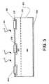
図3に示す実施態様は、基板の両面にコンタクトを必要とするため、光子が通過することができる前面の使用できる面積を減少する。太陽電池400の第2の実施態様の断面を図6に示す。基本的に、この実施態様の物理的過程は似ており、pn接合が、発生した電子孔対を分離する電界を創生するために、用いられる。しかしながら、前の実施態様でなされたように、全基板のいたる所にpn接合を創生するのではなく、pn接合を基板400の一部のみに創生する。この実施態様では、負にドープしたシリコン基板410を用いることができる。ある実施態様では、もっと負にバイアスをかけられた前面電界(FSF)420が、追加のn型ドーパントを前面に注入することにより、創生される。この前面は反射防止材料430で覆う。この前面は、表面積を増加するために、鋸歯状の又は非平面の表面を創生するためにエッチングすることがよくある。金属のコンタクト又は指状の物470a、470bは、全て、基板の底面に位置付ける。底面のある部分は、エミッタ440を創生するために、p型ドーパントで注入することができる。他の部分は、もっと負にバイアスをかけられた裏面電界450を創生するために、n型ドーパントで注入する。裏面は、裏面の反射性を高めるために、誘電体層460で覆う。金属の指状の物470aは、エミッタ440に取り付けて、指状の物470bは、裏面電界450に取り付ける。図7は、裏面のコンタクトの一般的な構造を示す。このタイプの太陽電池は、相互嵌合型バックコンタクト(IBC)太陽電池として知られる。The embodiment shown in FIG. 3 requires contact on both sides of the substrate, thus reducing the usable area of the front surface through which photons can pass. A cross section of a second embodiment of
現在のエネルギーコストと環境への関心から、太陽電池は、ますます重要になっている。高性能太陽電池の製造又は生産のコストの削減又は高性能太陽電池の効率の改善により、太陽電池の推進に世界的なプラスの効果をもたらす。これにより、このクリーンエネルギー技術のより広い利用性を可能にする。 Solar cells are becoming increasingly important due to current energy costs and environmental concerns. Reducing the cost of manufacturing or producing high performance solar cells or improving the efficiency of high performance solar cells has a positive global effect on the promotion of solar cells. This allows wider availability of this clean energy technology.
現在の太陽電池の設計は、ドーパントを太陽電池のシリコンの中へ拡散することにより実現できる、ドーパントプロファイルにより制限される。それは、異なるドーパントを適用すること及び太陽電池の異なる部分にドーピングすることの困難性によっても制限される。追加のドーピングステップのコストは、商業ベースで利用することができる太陽電池の設計を制限する。従って、太陽電池の改善したイオン注入、特に、イオン注入装置で太陽電池の連続ドーピングステップを可能にする方法の技術の必要性がある。 Current solar cell designs are limited by the dopant profile that can be achieved by diffusing the dopant into the silicon of the solar cell. It is also limited by the difficulty of applying different dopants and doping different parts of the solar cell. The cost of the additional doping step limits the design of solar cells that can be utilized on a commercial basis. Accordingly, there is a need for improved ion implantation of solar cells, and in particular, a technique for a method that allows a continuous doping step of solar cells with an ion implanter.
太陽電池の製造は、本明細書に開示された方法の使用により、単純化され、コストは減少する。連続注入を真空破壊せずに行うことにより、太陽電池をもっと迅速に製造することができる。さらに、連鎖注入の使用により、太陽電池の製造性能も向上することができる。一実施態様では、2つの注入を行い、同じイオン種を用いるが、2つの注入間で注入エネルギーを変更する。別の実施態様では、基板は、アニールする前に、両表面をひっくり返し注入する。さらに別の実施態様では、1つ以上の異なるマスクを当てて、注入を真空状態を破壊せずに行う。The manufacture of solar cells is simplified and the cost is reduced by using the methods disclosed herein. By performing continuous injection without breaking the vacuum, the solar cell can be manufactured more quickly. Furthermore, the use of chain injection can also improve the manufacturing performance of the solar cell. In one embodiment, two implants are made and the same ion species is used, but the implant energy is changed between the two implants. In another embodiment, the substrate is implanted with both surfaces turned over prior to annealing. In yet another embodiment, by applying one or more different masks,intends line without breaking the vacuuminjection.
本開示をより良く理解するために、本明細書に参照により組み込まれる、以下の添付図面を参照する。 For a better understanding of the present disclosure, reference is made to the following accompanying drawings, which are hereby incorporated by reference.
図1は、選択した材料をドーピングするためイオンを供給することができるプラズマドーピングシステム100のブロック図である。図2は、選択した材料をドーピングするためイオンを供給することができるビームラインイオン注入装置200のブロック図である。当業者は、プラズマドーピングシステム100及びビームラインイオン注入装置200が、選択した材料をドーピングするためイオンを供給することができる異なるプラズマドーピングシステム及びビームラインイオン注入装置の多くの例の内の各々ただ1つの例であることを、認識するであろう。このプロセスは、非質量分析大量注入装置(non-mass analyzed flood implanter)、他の基板又は半導体ウエハ処理装置、又は2つ以上のこれらのシステムのある組み合わせのような他のイオン注入システムと共に、行うこともできる。 FIG. 1 is a block diagram of a
図1を参照するに、プラズマドーピングシステム100は、包囲した容積103を規定するプロセスチャンバ102を含む。プラテン134は、基板138を支持するために、プロセスチャンバ102内で位置付けることができる。一例では、基板138は、一実施形態で、300mmの直径のシリコンウエハのような円盤形状を有する半導体基板とすることができる。この基板138は、太陽電池とすることができる。基板138は、静電力又は機械的力により、プラテン134の平坦面にクランプすることができる。一実施形態では、プラテン134は、基板138に接続するための導電ピン(図示せず)を含むことができる。 Referring to FIG. 1, the
ガス源104は、質量流量コントローラ106を介して、プロセスチャンバ102の内部容積103にドーパントガスを供給する。ガスバッフル170は、ガス源104からのガス流を偏向させるために、プロセスチャンバ102内で位置付ける。圧力計108は、プロセスチャンバ102内の圧力を測定する。真空ポンプ112は、プロセスチャンバ102内の排気口110を介して、プロセスチャンバ102から排ガスを排出する。排気弁114は、排気口110を介して排気伝導率を制御する。 The
プラズマドーピングシステム100は、質量流量コントローラ106、圧力計108及び排気弁114に電気的に接続されたガス圧コントローラ116を、さらに含むことができる。ガス圧コントローラ116は、圧力計108に応答するフィードバックループ内で、排気弁114で排気伝導率を制御するか、それとも、質量流量コントローラ106でプロセスガス流速度を制御するかにより、プロセスチャンバ102内の所望の圧力を維持するように構成することができる。 The
プロセスチャンバ102は、誘電材料で作られ、ほぼ水平方向に延びる第1の区分120を含むチャンバ頂部118を有することができる。チャンバ頂部118は、誘電材料で作られ、ほぼ垂直方向に第1の区分120から高く延びる第2の区分122も含む。チャンバ頂部118は、導電性及び伝熱性のある材料で作られ、ほぼ水平方向に第2の区分122の間に延びる蓋124を、さらに含む。 The
プラズマドーピングシステム100は、プロセスチャンバ102内にプラズマ140を発生するように構成される源101を、さらに含むことができる。源101は、プラズマ140を発生するために、平面アンテナ126及びらせんアンテナ146のいずれか又は両方にRFパワーを供給する電源のようなRF源150を含むことができる。RF源150は、RF源150からRFアンテナ126、146へ送られるパワーを最大にするために、RF源150の出力インピーダンスをRFアンテナ126、146のインピーダンスにマッチさせるインピーダンスマッチングネットワークにより、RFアンテナ126、146に結合することができる。The
プラズマドーピングシステム100は、プラテン134に電気的に接続されたバイアス電源148も含むことができる。バイアス電源148は、プラテン134にバイアスをかけ、よって、基板138にもバイアスをかけて、パルスがオフの期間ではなく、パルスがオンの期間にプラズマ140から基板138へイオンを加速するために、パルスがオン及びオフの期間を有するパルスプラテン信号を供給するように構成される。バイアス電源148は、DC電源又はRF電源とすることができる。 The
プラズマドーピングシステム100は、プラテン134の周りに配置された遮蔽リング194を、さらに含むことができる。技術的に知られるように、遮蔽リング194は、基板138のエッジの近くの注入されたイオン分布の均一性を改善するために、バイアスをかけることができる。環状ファラデーセンサ199のような1つ以上のファラデーセンサは、イオンビーム電流を感知するために、遮蔽リング194内に位置付けるkとができる。 The
プラズマドーピングシステム100は、コントローラ156及びユーザインターフェースシステム158を、さらに含むことができる。コントローラ156は、所望の入力/出力機能を行うためにプログラムすることができる、汎用コンピュータ又は汎用コンピュータのネットワークにすることができ、又はそれを含むことができる。コントローラ156は、特定用途向け集積回路、他のハード・ワイヤードの又はプログラム可能な電子機器、離散素子回路等のような他の電子回路又は電子部品も含むことができる。コントローラ156は、通信機器、データ記憶機器及びソフトウェアも含むことができる。例示の明確化のため、コントローラ156は、電源148への出力信号のみを供給するとして、かつ、ファラデーセンサ199から入力信号を受信するとして、例示する。当業者は、コントローラ156が、プラズマドーピングシステム100の他の構成部品へ出力信号を供給し、同じ構成部品から入力信号を受信することができることを認識するであろう。ユーザインターフェースシステム158は、タッチスクリーン、キーボード、ユーザ・ポインティング・デバイス、ディスプレー、プリンタ等のような機器を含むことができ、ユーザが、コントローラ156により、コマンド及び/若しくはデータを入力し、並びに/又は、プラズマドーピングシステム100をモニタすることを可能にする。The
動作中、ガス源104は、基板138に注入するため、所望のドーパントを含む主要なドーパントガスを供給する。ガス圧コントローラ116は、主要なドーパントガスをプロセスチャンバ102に供給する速度を調整する。源101は、プロセスチャンバ102内にプラズマ140を発生するように構成する。源101は、コントローラ156により制御することができる。プラズマ140を発生するために、RF源150は、少なくとも1つのRFアンテナ126、146でRF電流に共振して、振動磁界を生成する。振動磁界は、プロセスチャンバ102内にRF電流を誘導する。プロセスチャンバ102内のRF電流は、主要なドーパントガスを励起し電離して、プラズマ140を発生する。 In operation, the
バイアス電源148は、プラテン134にバイアスをかけ、よって、基板138にもバイアスをかけて、パルスプラテン信号のパルスがオンの期間に、プラズマ140から基板138へイオンを加速するために、パルスプラテン信号を供給する。パルスプラテン信号の周波数及び/又はパルスのデューティサイクルは、所望の線量率を供給するために、選択することができる。パルスプラテン信号の振幅は、所望のエネルギーを供給するために、選択することができる。他のパラメータが等しくありながら、より大きいエネルギーにより、より深い注入深さになる。 The
図2を参照するに、選択した材料をドーピングするためのイオンを供給することができるビームラインイオン注入装置200のブロック図を例示してある。当業者は、このビームラインイオン注入装置200は、選択した材料をドーピングするためのイオンを供給することができるビームラインイオン注入装置の多くの例のうちの1つにすぎないことを、認識するであろう。 Referring to FIG. 2, a block diagram of a beamline ion implanter 200 that can supply ions for doping a selected material is illustrated. Those skilled in the art will recognize that this beamline ion implanter 200 is just one of many examples of beamline ion implanters that can supply ions for doping a selected material. Will.
一般に、ビームラインイオン注入装置200は、イオンビーム281を形成するイオンを発生するためのイオン源280を含む。イオン源280は、イオンチャンバ283及びイオン化すべきガスを収容できるガスボックスを含むことができる。ガスはそれをイオン化するイオンチャンバ283へ供給される。このようにして形成されるイオンはイオンチャンバ283から取り出されて、イオンビーム281を形成する。イオンビーム281は分解磁石282の極の間に向けられる。電源がイオン源280の引き出し電極に接続されて、高電流イオン注入装置では、例えば約0.2kVと80kVとの間の可調整電圧を供給する。こうして、イオン源280からの一価のイオンが、この可調整電圧により、約0.2keVから80keVまでのエネルギーに加速される。In general, the beamline ion implanter 200 includes an ion source 280 for generating ions that form an ion beam 281. The ion source 280 can include an
イオンビーム281は、抑制電極284及び接地電極285を経て質量分析器286と進む。質量分析器286は、分解磁石282及び分解アパーチャ289を有するマスキング電極288を含む。分解磁石282は、所望イオン種のイオンが、分解アパーチャ289を通過するように、イオンビーム281内のイオンを偏向させる。不所望なイオン種は、分解アパーチャ289を通過しないで、マスキング電極288によりブロックされる。一実施態様では、分解磁石282は、所望のイオン種を約90°だけ偏向させる。 The ion beam 281 travels with the mass analyzer 286 through the
所望イオン種のイオンは、分解アパーチャ289を通って角度補正磁石294へと進む。角度補正磁石294は、所望イオン種のイオンを偏向させて、イオンビームを発散イオンビームからほぼ平行なイオンの軌道を有するリボンイオンビーム212に変換する。一実施態様では、角度補正磁石294は、所望イオン種のイオンを約70°だけ偏向させる。ビームラインイオン注入装置200は、いくつかの実施態様では、加速装置又は減速装置をさらに含むことができる。 Ions of the desired ion species travel through the resolving aperture 289 to the
エンドステーション211は、リボンイオンビーム212の経路内に、基板138のような1つ以上のワークピースを所望イオン種のイオンが基板138に注入されるように支持する。基板138は、例えば、シリコンウエハとすることができる。この基板138は、太陽電池とすることができる。エンドステーション211は、基板138を支持するプラテン295を含むことができる。エンドステーション211は、リボンイオンビーム212の長い横断面方向に対して垂直にワークピース138を動かし、それにより、基板138の全表面にイオンを分布させるスキャナー(図示せず)も含むことができる。リボンイオンビーム212を例示しているけれども、他の実施態様では、スポットビームとすることができる。
イオン注入装置は、当業者に知られた追加の構成部品を含むことができる。例えば、エンドステーション211は、典型的には、ワークピースをビームラインイオン注入装置200に導入して、イオン注入後にワークピースを取り外すための、自動ワークピース処理装置を含む。エンドステーション211は、線量測定システム、電子フラッドガン又は他の既知の構成部品も含むことができる。イオンビームが進行する全経路は、イオン注入の間、排気させることは、当業者に理解されるであろう。ビームラインイオン注入装置200は、いくつかの実施態様では、イオンのホット又はコールド注入を受け入れることができる。 The ion implanter can include additional components known to those skilled in the art. For example, the
生産性及び太陽電池の効率は、2つ以上の注入を行うことにより増加することができる。これらは、「連鎖注入」、すなわち、直後に次々と注入することのように、真空破壊せずに、同じ注入ツールで行う。コストを減少し、生産性及び太陽電池の効率を向上することに加えて、この方法は、ドーパントのプロファイルを、さらに改善することができる。連鎖注入を太陽電池の生産プロセスに組み入れることができる多くの異なる方法がある。これらのプロセスは、図1のプラズマドーピングシステム100、図2のビームラインイオン注入装置200、非質量分析大量注入装置(non-mass analyzed flood implanter)のような他のイオン注入システム、他の基板又は半導体ウエハ処理装置、又は2つ以上のこれらのシステムのある組み合わせの、いずれかで行うことができる。 Productivity and solar cell efficiency can be increased by performing more than one injection. These are performed with the same injection tool without breaking the vacuum, as in "chain injection", i.e. one after another. In addition to reducing costs and improving productivity and solar cell efficiency, this method can further improve the dopant profile. There are many different ways that chain injection can be incorporated into the solar cell production process. These processes can include
第1に、異なるエネルギーでの2つ以上の注入を連鎖注入で行うことができる。エネルギーの範囲により、ドーパントのプロファイルの詳細な調整を可能にする。例えば、図3で示すように、前面接触の太陽電池での、エミッタ330のドーピング用に、コンタクト350aの接合の短絡を防ぐために、深くより低い線量の注入を行うことができる。太陽電池の表面でのドーパントの高濃度を創生するために、浅くより高い線量の注入を行うこともできる。この注入の組み合わせにより、前面から後面に変わることを減少するドーパントのプロファイルを創生する。そのようなプロファイルは、少数キャリアをpn接合の方へ加速する有向の電界を創生することにより、再結合を最小にすることもできる。特定の実施形態では、図2のビームラインイオン注入装置200のビームエネルギーは、ビームがプラテン上の太陽電池に達する前に、減速電圧を加えることにより、変更することができる。First, two or more injections with different energies can be performed by chain injection. The range of energy allows fine tuning of the dopant profile. For example, as shown in Figure 3, in the solar cell front contact, for doping of the
第2に、異なる種の注入は、基板を動かさない連鎖注入で行うことができる。一実施形態では、リンに加えて、ヒ素をn型ドーパントとして用いる。後の熱的プロセスは、それから、これらの2つのn型ドーパントの異なる性質を利用する。例えば、1方のドーパントは、基板により深く拡散することができ、他方のドーパントは、表面により近くとどまり、これにより、ドーパント勾配を創生する。このドーパント勾配は、表面の再結合を最小にするのに役立つ。他の実施形態では、ホウ素、ヒ素、リン、ガリウム、アルミニウム又は他の当業者に既知の種を用いることができる。他の実施形態では、炭素、シリコン、ゲルマニウムのようなIV族に属する元素のような非ドーパントとしても知られる、ドーピング濃度に影響を与えない種を用いることができる。図1のプラズマドーピングシステム100又は図2のビームラインイオン注入装置200のようなイオン注入装置内の拡散炉内で種を変更することは、困難であるが、種を変更することは、イオン源、ビームライン、又は、ドーパント原子を供給するために用いるガス又は固体の材料を変更することにより、行うことができる。これにより、図1のプラズマドーピングシステム100又は図2のビームラインイオン注入装置200の複雑性及びコストを増加するが、この増加は、第2の注入装置を購入するより著しく少ない。 Secondly, different species of implantation can be performed by chain implantation without moving the substrate. In one embodiment, arsenic is used as an n-type dopant in addition to phosphorus. Later thermal processes then take advantage of the different properties of these two n-type dopants. For example, one dopant can diffuse deeper into the substrate while the other dopant stays closer to the surface, thereby creating a dopant gradient. This dopant gradient helps to minimize surface recombination. In other embodiments, boron, arsenic, phosphorus, gallium, aluminum, or other species known to those skilled in the art can be used. In other embodiments, species that do not affect the doping concentration, also known as non-dopants, such as elements belonging to Group IV, such as carbon, silicon, germanium, can be used. It is difficult to change the species in a diffusion furnace in an ion implanter, such as the
第3に、注入される基板の側面は、連鎖注入の間に変更することができる。基板を注入の間にひっくり返すことにより、第2の注入は、真空破壊せずに、反対側面に直ちに行うことができる。このひっくり返しは、例えば、ロボットの基板操作装置により、遂行することができる。一実施形態では、基板のひっくり返しを、注入される種の変更と組み合わせる。例えば、図6に示すように、イオンをIBC太陽電池の両側表面上に注入する。n+注入420は前面で行い、一方、n+注入450及びp+注入440の両方は背面で行う。従って、前面での注入を行うことができて、それから、太陽電池のホウ素の背面電界を遂行することができるように、基板をひっくり返すことができる。別の特定の実施形態では、前面電界の移植及びIBC太陽電池上の一組のコンタクトを遂行する。別の実施形態では、図6に示すように、n+前面電界及びn+背面電界をかける。現在の拡散技術では、異なる太陽電池の側面に、異なる線量を加えることはできない。真空破壊せずに、基板の両側表面に注入することにより、太陽電池の製造のための多くの必要なプロセスステップを減少することができる。 Third, the side of the substrate to be implanted can be changed during chain implantation. By flipping the substrate during implantation, the second implantation can be done immediately on the opposite side without breaking the vacuum. This overturning can be performed by, for example, a robot substrate operating device. In one embodiment, turning the substrate over is combined with a change in the species being implanted. For example, as shown in FIG. 6, ions are implanted on both side surfaces of the IBC solar cell. The n +
第4に、注入のパターンは、連鎖注入の間に変更することができる。マスクを挿入することにより、又はいくつかのマスクを基板に当てることにより、太陽電池の表面への異なる分布の多数の注入を行うことができる。このマスクは、いくつかの実施形態では、基板の部分を注入からブロックするハードマスク、シャドウマスク又はステンシルマスクとすることができる。特定の実施形態では、図5の太陽電池の前面をドープする。それから、コンタクト領域370のみがさらされるように、マスクを基板上に置く。それから、コンタクト領域370の導電率を改善するために、より高い線量の第2の注入を行う。別の実施形態では、図6及び7で示すようなIBC太陽電池のn+背面電界は、n+型ドーパントで注入し、一方、表面の一部を覆うために、マスクを用いる。それから、p+エミッタのみがさらされる状態にする第2のマスクを用いる。そのようなマスクを図8に示す。マスクの配置後に、p型ドーパントを注入する。異なるマスクでの注入のこの連続により、IBC太陽電池に必要なコンタクトパターンを創生することができる。従って、種の変更と組み合わせると、IBC太陽電池の全ての背面コンタクトドーピングは、同時に行うことができる。任意の実施形態では、コンタクトは、この方法で、太陽電池の前面又は背面のいずれかにドープすることができる。埋め込みコンタクトアプローチは、より高いコストでの同様のドーピングスキームを可能にする。別の実施形態では、n++注入をマスク付きで行い、それから、n+注入をマスクなしで行う。Fourth, the pattern of implantation can be changed during chain implantation. Multiple implantations of different distributions on the surface of the solar cell can be performed by inserting a mask or by applying several masks to the substrate. This mask may in some embodiments be a hard mask, shadow mask or stencil mask that blocks portions of the substrate from implantation. In certain embodiments, the front surface of the solar cell of FIG. 5 is doped. A mask is then placed on the substrate so that only the
第5に、連鎖注入後の即時熱的アニールは、注入が行われたのと同じチャンバ内で行うことができる。これにより、処理時間及びコストの減少を可能にする。注入チャンバ内で行われるこのアニールは、例えば、フラッシュアニール、レーザーアニール、スパイクアニール、又は、当業者に既知の他のアニール方法とすることができる。 Fifth, immediate thermal annealing after chain implantation can be performed in the same chamber where the implantation was performed. Thereby, the processing time and cost can be reduced. This annealing performed in the implantation chamber can be, for example, flash annealing, laser annealing, spike annealing, or other annealing methods known to those skilled in the art.
第6に、これらの連鎖注入は、クラスターツールで行うことができる。クラスターツールは、特定の実施形態の図1に示すような多数のプラズマドーピングシステム100を組み込むことができる。従って、連鎖注入は、真空破壊せずに多数のプラズマドーピングチャンバ内で行うことができるか、又は、単一のプラズマドーピングチャンバ内で多数の注入で行うことができる。 Sixth, these chain injections can be performed with a cluster tool. The cluster tool can incorporate a number of
本明細書で用いている用語及び表現は、説明の用語として用い、限定の用語として用いてはおらず、そのような用語及び表現の使用では、示され説明された(又はそれらの部分の)特徴の任意の均等物を除外する意図はない。本特許請求の範囲内で様々な変更ができることも認められる。他の変更、変形および代替も可能である。従って、前述の説明は単に例によるものであり、限定することを意図するものではない。 The terms and expressions used herein are used as descriptive terms and are not used as limiting terms, and the use of such terms and expressions may be shown and described (or parts thereof). There is no intention to exclude any equivalent of. It will be appreciated that various modifications can be made within the scope of the claims. Other modifications, variations and alternatives are possible. Accordingly, the foregoing description is by way of example only and is not intended as limiting.
Claims (16)
Translated fromJapanese前記方法は、
前記太陽電池を製造するために、前記基板が注入されるべき真空を創生するステップと、
第1の種を用いて前記基板の第1の表面の全体に前記真空中で第1のイオン注入を行うステップと、
前記基板の前記第1の表面に面し、かつ、前記基板の前記第1の表面から相隔たる第1の表面を有するマスクを前記真空中に導入するステップと、前記基板の前記第1の表面の対応する部分をさらすために、前記マスクは複数の開口を有し、
第2の種を用いて前記基板の前記第1の表面に前記真空中で第2のイオン注入を行うステップであって、前記基板の前記第1の表面の前記さらした部分のみに前記第2の種を用いてイオン注入を行うステップと、を有し、
前記第1のイオン注入、前記第2のイオン注入及び前記マスクの導入を単一のチャンバ内で真空破壊せずに行う、基板を使用して太陽電池を製造する方法。A method of manufacturing a solar cell using a substrate,
The method
In order to manufacture the solar cell, comprising the steps of creation of a vacuumto the substrate it is injected,
Performing a first ion implantationin thevacuum onthe entire first surface of the substrate using a first species;
Facing the first surface of the substrate, and introducinga maskhaving a first surface spaced-apart from said first surface of said substratein said vacuum, said substrate said first Themask has a plurality of openings toexpose corresponding portions of the surface;
Wherein a second step of performing ion implantationin vacuum on the first surfaceof the substrate using a secondspecies, the onlythe exposed portion of said first surfacebefore Symbol substrate first Performing ion implantation using two species,
The first ion implantation is performed without vacuum break of the introductionof the second ion implantation and themask in a single chamber, the method for manufacturing the solar cell using the substrate.
前記方法は、
前記太陽電池を製造するために、前記基板が注入されるべき真空を創生するステップと、
第1の種を用いて前記基板の第1の表面の全体に前記真空中で第1のイオン注入を行うステップと、
前記基板の第2の表面をさらすために、前記基板を前記真空中でひっくり返すステップと、
前記基板の前記第2の表面に面し、かつ、前記基板の前記第2の表面から相隔たる第1の表面を有するマスクを前記真空中に導入するステップと、前記基板の前記第2の表面の対応する部分をさらすために、前記マスクは複数の開口を有し、
第2の種を用いて前記基板の前記第2の表面に前記真空中で第2のイオン注入を行うステップであって、前記基板の前記第2の表面の前記さらした部分のみに前記第2の種を用いてイオン注入を行うステップと、を有し、
前記第1のイオン注入、前記第2のイオン注入、前記基板のひっくり返し及び前記マスクの導入を単一のチャンバ内で真空破壊せずに行う、基板を使用して太陽電池を製造する方法。A method of manufacturing a solar cell using a substrate,
The method
In order to manufacture the solar cell, comprising the steps of creation of a vacuumto the substrate it is injected,
Performing a first ion implantationin thevacuum onthe entire first surface of the substrate using a first species;
Inverting the substrate in thevacuum to expose the second surface of the substrate;
Facing the second surface of the substrate, and introducinga maskhaving a first surface spaced-apart from said second surface of said substratein said vacuum, said second of said substrate Themask has a plurality of openings toexpose corresponding portions of the surface;
Wherein a second step of performing ion implantationin a vacuum to the second surfaceof the substrate using a secondspecies, the onlythe exposed portion of said second surfaceprior Stories substrate first Performing ion implantation using two species,
Method for producing the first ion implantation is performed without vacuum break the second ion implantation, the flipped and introductionof themask of the substrate in a single chamber, the solar cell using the substrate .
前記方法は、
前記太陽電池を製造するために、前記基板が注入されるべき真空を創生するステップと、
第1の種を用いて前記基板の第1の表面の全体に前記真空中で第1のイオン注入を行うステップと、
前記基板の第2の表面をさらすために、前記基板を前記真空中でひっくり返すステップと、
第2の種を用いて前記基板の前記第2の表面に前記真空中で第2のイオン注入を行うステップと、を有し、
前記第1のイオン注入、前記第2のイオン注入及び前記基板のひっくり返しを単一のチャンバ内で真空破壊せずに行う、基板を使用して太陽電池を製造する方法。A method of manufacturing a solar cell using a substrate,
The method
In order to manufacture the solar cell, comprising the steps of creation of a vacuumto the substrate it is injected,
Performing a first ion implantationin thevacuum onthe entire first surface of the substrate using a first species;
Inverting the substrate in thevacuum to expose the second surface of the substrate;
Performing a second ion implantationin thevacuum on the second surface of thesubstrate using a second species;
A method of manufacturing a solar cell using a substrate, wherein the first ion implantation, the second ion implantation, and the turning over of the substrate are performed in a single chamber without vacuum break.
前記マスクは、前記基板の前記第2の表面に面し、かつ、前記基板の前記第2の表面から相隔たる第1の表面を有し、
前記基板の前記第2の表面のさらした部分のみに前記第2の種を用いてイオン注入を行うように、前記基板の前記第2の表面の対応する部分をさらすために、前記マスクは複数の開口を有する、請求項11に記載の方法。Prior to said second ion implantation,is introducedwithout vacuum break of the mask in the vacuum,
The mask has a first surface facing the second surface of the substrate and spaced apart from the second surface of the substrate;
Inorder to expose a corresponding portion of the second surface of the substrate such that only theexposed portion of the second surface of the substrate is ion implanted using the second species, the mask includes a plurality of masks. tohave the opening, the method of claim11.
Applications Claiming Priority (5)
| Application Number | Priority Date | Filing Date | Title |
|---|---|---|---|
| US3387308P | 2008-03-05 | 2008-03-05 | |
| US61/033,873 | 2008-03-05 | ||
| US12/397,634 | 2009-03-04 | ||
| US12/397,634US7727866B2 (en) | 2008-03-05 | 2009-03-04 | Use of chained implants in solar cells |
| PCT/US2009/036232WO2009111665A2 (en) | 2008-03-05 | 2009-03-05 | Use of chained implants in solar cells |
Publications (3)
| Publication Number | Publication Date |
|---|---|
| JP2011513997A JP2011513997A (en) | 2011-04-28 |
| JP2011513997A5 JP2011513997A5 (en) | 2014-10-23 |
| JP5802392B2true JP5802392B2 (en) | 2015-10-28 |
Family
ID=41054056
Family Applications (1)
| Application Number | Title | Priority Date | Filing Date |
|---|---|---|---|
| JP2010549895AExpired - Fee RelatedJP5802392B2 (en) | 2008-03-05 | 2009-03-05 | Method for manufacturing a solar cell using a substrate |
Country Status (7)
| Country | Link |
|---|---|
| US (2) | US7727866B2 (en) |
| EP (2) | EP2858126B1 (en) |
| JP (1) | JP5802392B2 (en) |
| KR (1) | KR101409925B1 (en) |
| CN (1) | CN102047390B (en) |
| TW (1) | TWI443718B (en) |
| WO (1) | WO2009111665A2 (en) |
Families Citing this family (425)
| Publication number | Priority date | Publication date | Assignee | Title |
|---|---|---|---|---|
| US8420435B2 (en)* | 2009-05-05 | 2013-04-16 | Solexel, Inc. | Ion implantation fabrication process for thin-film crystalline silicon solar cells |
| US8461032B2 (en)* | 2008-03-05 | 2013-06-11 | Varian Semiconductor Equipment Associates, Inc. | Use of dopants with different diffusivities for solar cell manufacture |
| US20090317937A1 (en)* | 2008-06-20 | 2009-12-24 | Atul Gupta | Maskless Doping Technique for Solar Cells |
| CN102150278A (en)* | 2008-06-11 | 2011-08-10 | 因特瓦克公司 | Formation of solar cell-selective emitter using implant and anneal method |
| US20100154870A1 (en)* | 2008-06-20 | 2010-06-24 | Nicholas Bateman | Use of Pattern Recognition to Align Patterns in a Downstream Process |
| US10378106B2 (en) | 2008-11-14 | 2019-08-13 | Asm Ip Holding B.V. | Method of forming insulation film by modified PEALD |
| US9394608B2 (en) | 2009-04-06 | 2016-07-19 | Asm America, Inc. | Semiconductor processing reactor and components thereof |
| US9006688B2 (en)* | 2009-04-08 | 2015-04-14 | Varian Semiconductor Equipment Associates, Inc. | Techniques for processing a substrate using a mask |
| US8900982B2 (en)* | 2009-04-08 | 2014-12-02 | Varian Semiconductor Equipment Associates, Inc. | Techniques for processing a substrate |
| US8563407B2 (en)* | 2009-04-08 | 2013-10-22 | Varian Semiconductor Equipment Associates, Inc. | Dual sided workpiece handling |
| US9076914B2 (en)* | 2009-04-08 | 2015-07-07 | Varian Semiconductor Equipment Associates, Inc. | Techniques for processing a substrate |
| US8330128B2 (en)* | 2009-04-17 | 2012-12-11 | Varian Semiconductor Equipment Associates, Inc. | Implant mask with moveable hinged mask segments |
| US9318644B2 (en) | 2009-05-05 | 2016-04-19 | Solexel, Inc. | Ion implantation and annealing for thin film crystalline solar cells |
| US20110027463A1 (en)* | 2009-06-16 | 2011-02-03 | Varian Semiconductor Equipment Associates, Inc. | Workpiece handling system |
| US8749053B2 (en) | 2009-06-23 | 2014-06-10 | Intevac, Inc. | Plasma grid implant system for use in solar cell fabrications |
| US8008176B2 (en)* | 2009-08-11 | 2011-08-30 | Varian Semiconductor Equipment Associates, Inc. | Masked ion implant with fast-slow scan |
| US8802201B2 (en) | 2009-08-14 | 2014-08-12 | Asm America, Inc. | Systems and methods for thin-film deposition of metal oxides using excited nitrogen-oxygen species |
| US8603900B2 (en)* | 2009-10-27 | 2013-12-10 | Varian Semiconductor Equipment Associates, Inc. | Reducing surface recombination and enhancing light trapping in solar cells |
| US8465909B2 (en)* | 2009-11-04 | 2013-06-18 | Varian Semiconductor Equipment Associates, Inc. | Self-aligned masking for solar cell manufacture |
| US8461030B2 (en) | 2009-11-17 | 2013-06-11 | Varian Semiconductor Equipment Associates, Inc. | Apparatus and method for controllably implanting workpieces |
| US8153456B2 (en)* | 2010-01-20 | 2012-04-10 | Varian Semiconductor Equipment Associates, Inc. | Bifacial solar cell using ion implantation |
| US8735234B2 (en)* | 2010-02-18 | 2014-05-27 | Varian Semiconductor Equipment Associates, Inc. | Self-aligned ion implantation for IBC solar cells |
| US8921149B2 (en)* | 2010-03-04 | 2014-12-30 | Varian Semiconductor Equipment Associates, Inc. | Aligning successive implants with a soft mask |
| US8912082B2 (en)* | 2010-03-25 | 2014-12-16 | Varian Semiconductor Equipment Associates, Inc. | Implant alignment through a mask |
| US20110272024A1 (en)* | 2010-04-13 | 2011-11-10 | Applied Materials, Inc. | MULTI-LAYER SiN FOR FUNCTIONAL AND OPTICAL GRADED ARC LAYERS ON CRYSTALLINE SOLAR CELLS |
| US8071418B2 (en) | 2010-06-03 | 2011-12-06 | Suniva, Inc. | Selective emitter solar cells formed by a hybrid diffusion and ion implantation process |
| US8110431B2 (en)* | 2010-06-03 | 2012-02-07 | Suniva, Inc. | Ion implanted selective emitter solar cells with in situ surface passivation |
| US20110320030A1 (en)* | 2010-06-25 | 2011-12-29 | Varian Semiconductor Equipment Associates, Inc. | Thermal Control of a Proximity Mask and Wafer During Ion Implantation |
| US20110139231A1 (en) | 2010-08-25 | 2011-06-16 | Daniel Meier | Back junction solar cell with selective front surface field |
| US8216923B2 (en) | 2010-10-01 | 2012-07-10 | Varian Semiconductor Equipment Associates, Inc. | Integrated shadow mask/carrier for patterned ion implantation |
| US9231061B2 (en) | 2010-10-25 | 2016-01-05 | The Research Foundation Of State University Of New York | Fabrication of surface textures by ion implantation for antireflection of silicon crystals |
| US8242005B1 (en) | 2011-01-24 | 2012-08-14 | Varian Semiconductor Equipment Associates, Inc. | Using multiple masks to form independent features on a workpiece |
| TWI455340B (en)* | 2011-02-25 | 2014-10-01 | Gintech Energy Corp | Solar cell manufacturing method |
| US8153496B1 (en) | 2011-03-07 | 2012-04-10 | Varian Semiconductor Equipment Associates, Inc. | Self-aligned process and method for fabrication of high efficiency solar cells |
| EP2715797A4 (en)* | 2011-05-27 | 2015-05-27 | Solexel Inc | ION IMPLANTATION AND ANNEALING FOR HIGH EFFICIENCY SOLAR CELLS WITH REAR JUNCTION AND REAR CONTACT |
| US9312155B2 (en) | 2011-06-06 | 2016-04-12 | Asm Japan K.K. | High-throughput semiconductor-processing apparatus equipped with multiple dual-chamber modules |
| US8658458B2 (en)* | 2011-06-15 | 2014-02-25 | Varian Semiconductor Equipment Associates, Inc. | Patterned doping for polysilicon emitter solar cells |
| US20120322192A1 (en)* | 2011-06-15 | 2012-12-20 | Varian Semiconductor Equipment Associates, Inc. | Method of defect reduction in ion implanted solar cell structures |
| KR20120140026A (en)* | 2011-06-20 | 2012-12-28 | 엘지전자 주식회사 | Solar cell |
| US10364496B2 (en) | 2011-06-27 | 2019-07-30 | Asm Ip Holding B.V. | Dual section module having shared and unshared mass flow controllers |
| US8697559B2 (en) | 2011-07-07 | 2014-04-15 | Varian Semiconductor Equipment Associates, Inc. | Use of ion beam tails to manufacture a workpiece |
| US10854498B2 (en) | 2011-07-15 | 2020-12-01 | Asm Ip Holding B.V. | Wafer-supporting device and method for producing same |
| US20130023129A1 (en)* | 2011-07-20 | 2013-01-24 | Asm America, Inc. | Pressure transmitter for a semiconductor processing environment |
| KR101969032B1 (en)* | 2011-09-07 | 2019-04-15 | 엘지전자 주식회사 | Solar cell and manufacturing method thereof |
| US9190548B2 (en) | 2011-10-11 | 2015-11-17 | Varian Semiconductor Equipment Associates, Inc. | Method of creating two dimensional doping patterns in solar cells |
| US9017481B1 (en) | 2011-10-28 | 2015-04-28 | Asm America, Inc. | Process feed management for semiconductor substrate processing |
| US9437392B2 (en) | 2011-11-02 | 2016-09-06 | Varian Semiconductor Equipment Associates, Inc. | High-throughput ion implanter |
| SG11201402177XA (en) | 2011-11-08 | 2014-06-27 | Intevac Inc | Substrate processing system and method |
| KR20130050721A (en) | 2011-11-08 | 2013-05-16 | 삼성에스디아이 주식회사 | Solar cell |
| KR101875747B1 (en)* | 2011-12-16 | 2018-07-06 | 엘지전자 주식회사 | Method for manufacturing solar cell |
| FR2985605B1 (en)* | 2012-01-05 | 2014-10-17 | Commissariat Energie Atomique | METHOD FOR MANUFACTURING MICROELECTRONIC COMPONENT |
| JP5892802B2 (en) | 2012-02-09 | 2016-03-23 | 住友重機械工業株式会社 | Ion implantation method, transfer container, and ion implantation apparatus |
| KR101832230B1 (en) | 2012-03-05 | 2018-04-13 | 엘지전자 주식회사 | Solar cell and method for manufacturing the same |
| US9412895B2 (en)* | 2012-04-04 | 2016-08-09 | Samsung Sdi Co., Ltd. | Method of manufacturing photoelectric device |
| NL2008755C2 (en) | 2012-05-04 | 2013-11-06 | Tempress Ip B V | Method of manufacturing a solar cell and equipment therefore. |
| KR101879781B1 (en)* | 2012-05-11 | 2018-08-16 | 엘지전자 주식회사 | Solar cell, method for manufacturing dopant layer, and method for manufacturing solar cell |
| US9659799B2 (en) | 2012-08-28 | 2017-05-23 | Asm Ip Holding B.V. | Systems and methods for dynamic semiconductor process scheduling |
| US9021985B2 (en) | 2012-09-12 | 2015-05-05 | Asm Ip Holdings B.V. | Process gas management for an inductively-coupled plasma deposition reactor |
| US9082799B2 (en) | 2012-09-20 | 2015-07-14 | Varian Semiconductor Equipment Associates, Inc. | System and method for 2D workpiece alignment |
| US10714315B2 (en) | 2012-10-12 | 2020-07-14 | Asm Ip Holdings B.V. | Semiconductor reaction chamber showerhead |
| MY178951A (en) | 2012-12-19 | 2020-10-23 | Intevac Inc | Grid for plasma ion implant |
| US9196489B2 (en)* | 2013-01-25 | 2015-11-24 | Varian Semiconductor Equipment Associates, Inc. | Ion implantation based emitter profile engineering via process modifications |
| US20160376700A1 (en) | 2013-02-01 | 2016-12-29 | Asm Ip Holding B.V. | System for treatment of deposition reactor |
| TWI499059B (en)* | 2013-03-06 | 2015-09-01 | Neo Solar Power Corp | Block type doped solar cell |
| US9484191B2 (en) | 2013-03-08 | 2016-11-01 | Asm Ip Holding B.V. | Pulsed remote plasma method and system |
| US9589770B2 (en) | 2013-03-08 | 2017-03-07 | Asm Ip Holding B.V. | Method and systems for in-situ formation of intermediate reactive species |
| KR101613843B1 (en)* | 2013-04-23 | 2016-04-20 | 엘지전자 주식회사 | Solar cell and method for manufacturing the same |
| CN104425651B (en)* | 2013-09-09 | 2016-08-10 | 上海理想万里晖薄膜设备有限公司 | A low-temperature process for preparing heterojunction solar cells with no grid on the front |
| US9240412B2 (en) | 2013-09-27 | 2016-01-19 | Asm Ip Holding B.V. | Semiconductor structure and device and methods of forming same using selective epitaxial process |
| US9806220B2 (en)* | 2013-11-12 | 2017-10-31 | Ob Realty, Llc | Metal foil metallization for backplane-attached solar cells and modules |
| US9401450B2 (en) | 2013-12-09 | 2016-07-26 | Sunpower Corporation | Solar cell emitter region fabrication using ion implantation |
| US9577134B2 (en) | 2013-12-09 | 2017-02-21 | Sunpower Corporation | Solar cell emitter region fabrication using self-aligned implant and cap |
| US9722129B2 (en) | 2014-02-12 | 2017-08-01 | Varian Semiconductor Equipment Associates, Inc. | Complementary traveling masks |
| US10683571B2 (en) | 2014-02-25 | 2020-06-16 | Asm Ip Holding B.V. | Gas supply manifold and method of supplying gases to chamber using same |
| US10167557B2 (en) | 2014-03-18 | 2019-01-01 | Asm Ip Holding B.V. | Gas distribution system, reactor including the system, and methods of using the same |
| US11015245B2 (en) | 2014-03-19 | 2021-05-25 | Asm Ip Holding B.V. | Gas-phase reactor and system having exhaust plenum and components thereof |
| US9263625B2 (en) | 2014-06-30 | 2016-02-16 | Sunpower Corporation | Solar cell emitter region fabrication using ion implantation |
| US10858737B2 (en) | 2014-07-28 | 2020-12-08 | Asm Ip Holding B.V. | Showerhead assembly and components thereof |
| US9890456B2 (en) | 2014-08-21 | 2018-02-13 | Asm Ip Holding B.V. | Method and system for in situ formation of gas-phase compounds |
| US9657845B2 (en) | 2014-10-07 | 2017-05-23 | Asm Ip Holding B.V. | Variable conductance gas distribution apparatus and method |
| US10941490B2 (en) | 2014-10-07 | 2021-03-09 | Asm Ip Holding B.V. | Multiple temperature range susceptor, assembly, reactor and system including the susceptor, and methods of using the same |
| KR102300403B1 (en) | 2014-11-19 | 2021-09-09 | 에이에스엠 아이피 홀딩 비.브이. | Method of depositing thin film |
| KR102263121B1 (en) | 2014-12-22 | 2021-06-09 | 에이에스엠 아이피 홀딩 비.브이. | Semiconductor device and manufacuring method thereof |
| US10529542B2 (en) | 2015-03-11 | 2020-01-07 | Asm Ip Holdings B.V. | Cross-flow reactor and method |
| US10276355B2 (en) | 2015-03-12 | 2019-04-30 | Asm Ip Holding B.V. | Multi-zone reactor, system including the reactor, and method of using the same |
| US20160284913A1 (en) | 2015-03-27 | 2016-09-29 | Staffan WESTERBERG | Solar cell emitter region fabrication using substrate-level ion implantation |
| US10458018B2 (en) | 2015-06-26 | 2019-10-29 | Asm Ip Holding B.V. | Structures including metal carbide material, devices including the structures, and methods of forming same |
| US10600673B2 (en) | 2015-07-07 | 2020-03-24 | Asm Ip Holding B.V. | Magnetic susceptor to baseplate seal |
| US10043661B2 (en) | 2015-07-13 | 2018-08-07 | Asm Ip Holding B.V. | Method for protecting layer by forming hydrocarbon-based extremely thin film |
| US10083836B2 (en) | 2015-07-24 | 2018-09-25 | Asm Ip Holding B.V. | Formation of boron-doped titanium metal films with high work function |
| US9960072B2 (en) | 2015-09-29 | 2018-05-01 | Asm Ip Holding B.V. | Variable adjustment for precise matching of multiple chamber cavity housings |
| US10211308B2 (en) | 2015-10-21 | 2019-02-19 | Asm Ip Holding B.V. | NbMC layers |
| US10322384B2 (en) | 2015-11-09 | 2019-06-18 | Asm Ip Holding B.V. | Counter flow mixer for process chamber |
| US11139308B2 (en) | 2015-12-29 | 2021-10-05 | Asm Ip Holding B.V. | Atomic layer deposition of III-V compounds to form V-NAND devices |
| US10529554B2 (en) | 2016-02-19 | 2020-01-07 | Asm Ip Holding B.V. | Method for forming silicon nitride film selectively on sidewalls or flat surfaces of trenches |
| US10468251B2 (en) | 2016-02-19 | 2019-11-05 | Asm Ip Holding B.V. | Method for forming spacers using silicon nitride film for spacer-defined multiple patterning |
| US10501866B2 (en) | 2016-03-09 | 2019-12-10 | Asm Ip Holding B.V. | Gas distribution apparatus for improved film uniformity in an epitaxial system |
| US10343920B2 (en) | 2016-03-18 | 2019-07-09 | Asm Ip Holding B.V. | Aligned carbon nanotubes |
| US9892913B2 (en) | 2016-03-24 | 2018-02-13 | Asm Ip Holding B.V. | Radial and thickness control via biased multi-port injection settings |
| US10190213B2 (en) | 2016-04-21 | 2019-01-29 | Asm Ip Holding B.V. | Deposition of metal borides |
| US10087522B2 (en) | 2016-04-21 | 2018-10-02 | Asm Ip Holding B.V. | Deposition of metal borides |
| US10865475B2 (en) | 2016-04-21 | 2020-12-15 | Asm Ip Holding B.V. | Deposition of metal borides and silicides |
| US10032628B2 (en) | 2016-05-02 | 2018-07-24 | Asm Ip Holding B.V. | Source/drain performance through conformal solid state doping |
| US10367080B2 (en) | 2016-05-02 | 2019-07-30 | Asm Ip Holding B.V. | Method of forming a germanium oxynitride film |
| KR102592471B1 (en) | 2016-05-17 | 2023-10-20 | 에이에스엠 아이피 홀딩 비.브이. | Method of forming metal interconnection and method of fabricating semiconductor device using the same |
| US11453943B2 (en) | 2016-05-25 | 2022-09-27 | Asm Ip Holding B.V. | Method for forming carbon-containing silicon/metal oxide or nitride film by ALD using silicon precursor and hydrocarbon precursor |
| US10388509B2 (en) | 2016-06-28 | 2019-08-20 | Asm Ip Holding B.V. | Formation of epitaxial layers via dislocation filtering |
| US10612137B2 (en) | 2016-07-08 | 2020-04-07 | Asm Ip Holdings B.V. | Organic reactants for atomic layer deposition |
| US9859151B1 (en) | 2016-07-08 | 2018-01-02 | Asm Ip Holding B.V. | Selective film deposition method to form air gaps |
| US9793135B1 (en) | 2016-07-14 | 2017-10-17 | ASM IP Holding B.V | Method of cyclic dry etching using etchant film |
| US10714385B2 (en) | 2016-07-19 | 2020-07-14 | Asm Ip Holding B.V. | Selective deposition of tungsten |
| KR102354490B1 (en) | 2016-07-27 | 2022-01-21 | 에이에스엠 아이피 홀딩 비.브이. | Method of processing a substrate |
| US9887082B1 (en) | 2016-07-28 | 2018-02-06 | Asm Ip Holding B.V. | Method and apparatus for filling a gap |
| KR102532607B1 (en) | 2016-07-28 | 2023-05-15 | 에이에스엠 아이피 홀딩 비.브이. | Substrate processing apparatus and method of operating the same |
| US10177025B2 (en) | 2016-07-28 | 2019-01-08 | Asm Ip Holding B.V. | Method and apparatus for filling a gap |
| US9812320B1 (en) | 2016-07-28 | 2017-11-07 | Asm Ip Holding B.V. | Method and apparatus for filling a gap |
| US10395919B2 (en) | 2016-07-28 | 2019-08-27 | Asm Ip Holding B.V. | Method and apparatus for filling a gap |
| US10090316B2 (en) | 2016-09-01 | 2018-10-02 | Asm Ip Holding B.V. | 3D stacked multilayer semiconductor memory using doped select transistor channel |
| US10410943B2 (en) | 2016-10-13 | 2019-09-10 | Asm Ip Holding B.V. | Method for passivating a surface of a semiconductor and related systems |
| US10643826B2 (en) | 2016-10-26 | 2020-05-05 | Asm Ip Holdings B.V. | Methods for thermally calibrating reaction chambers |
| US11532757B2 (en) | 2016-10-27 | 2022-12-20 | Asm Ip Holding B.V. | Deposition of charge trapping layers |
| US10714350B2 (en) | 2016-11-01 | 2020-07-14 | ASM IP Holdings, B.V. | Methods for forming a transition metal niobium nitride film on a substrate by atomic layer deposition and related semiconductor device structures |
| US10435790B2 (en) | 2016-11-01 | 2019-10-08 | Asm Ip Holding B.V. | Method of subatmospheric plasma-enhanced ALD using capacitively coupled electrodes with narrow gap |
| US10643904B2 (en) | 2016-11-01 | 2020-05-05 | Asm Ip Holdings B.V. | Methods for forming a semiconductor device and related semiconductor device structures |
| US10229833B2 (en) | 2016-11-01 | 2019-03-12 | Asm Ip Holding B.V. | Methods for forming a transition metal nitride film on a substrate by atomic layer deposition and related semiconductor device structures |
| US10134757B2 (en) | 2016-11-07 | 2018-11-20 | Asm Ip Holding B.V. | Method of processing a substrate and a device manufactured by using the method |
| KR102546317B1 (en) | 2016-11-15 | 2023-06-21 | 에이에스엠 아이피 홀딩 비.브이. | Gas supply unit and substrate processing apparatus including the same |
| US10340135B2 (en) | 2016-11-28 | 2019-07-02 | Asm Ip Holding B.V. | Method of topologically restricted plasma-enhanced cyclic deposition of silicon or metal nitride |
| KR102762543B1 (en) | 2016-12-14 | 2025-02-05 | 에이에스엠 아이피 홀딩 비.브이. | Substrate processing apparatus |
| US11447861B2 (en) | 2016-12-15 | 2022-09-20 | Asm Ip Holding B.V. | Sequential infiltration synthesis apparatus and a method of forming a patterned structure |
| US9916980B1 (en) | 2016-12-15 | 2018-03-13 | Asm Ip Holding B.V. | Method of forming a structure on a substrate |
| US11581186B2 (en) | 2016-12-15 | 2023-02-14 | Asm Ip Holding B.V. | Sequential infiltration synthesis apparatus |
| KR102700194B1 (en) | 2016-12-19 | 2024-08-28 | 에이에스엠 아이피 홀딩 비.브이. | Substrate processing apparatus |
| US10269558B2 (en) | 2016-12-22 | 2019-04-23 | Asm Ip Holding B.V. | Method of forming a structure on a substrate |
| US10867788B2 (en) | 2016-12-28 | 2020-12-15 | Asm Ip Holding B.V. | Method of forming a structure on a substrate |
| US11390950B2 (en) | 2017-01-10 | 2022-07-19 | Asm Ip Holding B.V. | Reactor system and method to reduce residue buildup during a film deposition process |
| US10655221B2 (en) | 2017-02-09 | 2020-05-19 | Asm Ip Holding B.V. | Method for depositing oxide film by thermal ALD and PEALD |
| US10468261B2 (en) | 2017-02-15 | 2019-11-05 | Asm Ip Holding B.V. | Methods for forming a metallic film on a substrate by cyclical deposition and related semiconductor device structures |
| US10529563B2 (en) | 2017-03-29 | 2020-01-07 | Asm Ip Holdings B.V. | Method for forming doped metal oxide films on a substrate by cyclical deposition and related semiconductor device structures |
| US10283353B2 (en) | 2017-03-29 | 2019-05-07 | Asm Ip Holding B.V. | Method of reforming insulating film deposited on substrate with recess pattern |
| US10103040B1 (en) | 2017-03-31 | 2018-10-16 | Asm Ip Holding B.V. | Apparatus and method for manufacturing a semiconductor device |
| USD830981S1 (en) | 2017-04-07 | 2018-10-16 | Asm Ip Holding B.V. | Susceptor for semiconductor substrate processing apparatus |
| KR102457289B1 (en) | 2017-04-25 | 2022-10-21 | 에이에스엠 아이피 홀딩 비.브이. | Method for depositing a thin film and manufacturing a semiconductor device |
| US10446393B2 (en) | 2017-05-08 | 2019-10-15 | Asm Ip Holding B.V. | Methods for forming silicon-containing epitaxial layers and related semiconductor device structures |
| US10892156B2 (en) | 2017-05-08 | 2021-01-12 | Asm Ip Holding B.V. | Methods for forming a silicon nitride film on a substrate and related semiconductor device structures |
| US10770286B2 (en) | 2017-05-08 | 2020-09-08 | Asm Ip Holdings B.V. | Methods for selectively forming a silicon nitride film on a substrate and related semiconductor device structures |
| US10504742B2 (en) | 2017-05-31 | 2019-12-10 | Asm Ip Holding B.V. | Method of atomic layer etching using hydrogen plasma |
| US10886123B2 (en) | 2017-06-02 | 2021-01-05 | Asm Ip Holding B.V. | Methods for forming low temperature semiconductor layers and related semiconductor device structures |
| US12040200B2 (en) | 2017-06-20 | 2024-07-16 | Asm Ip Holding B.V. | Semiconductor processing apparatus and methods for calibrating a semiconductor processing apparatus |
| US11306395B2 (en) | 2017-06-28 | 2022-04-19 | Asm Ip Holding B.V. | Methods for depositing a transition metal nitride film on a substrate by atomic layer deposition and related deposition apparatus |
| US10685834B2 (en) | 2017-07-05 | 2020-06-16 | Asm Ip Holdings B.V. | Methods for forming a silicon germanium tin layer and related semiconductor device structures |
| KR20190009245A (en) | 2017-07-18 | 2019-01-28 | 에이에스엠 아이피 홀딩 비.브이. | Methods for forming a semiconductor device structure and related semiconductor device structures |
| US11374112B2 (en) | 2017-07-19 | 2022-06-28 | Asm Ip Holding B.V. | Method for depositing a group IV semiconductor and related semiconductor device structures |
| US10541333B2 (en) | 2017-07-19 | 2020-01-21 | Asm Ip Holding B.V. | Method for depositing a group IV semiconductor and related semiconductor device structures |
| US11018002B2 (en) | 2017-07-19 | 2021-05-25 | Asm Ip Holding B.V. | Method for selectively depositing a Group IV semiconductor and related semiconductor device structures |
| US10312055B2 (en) | 2017-07-26 | 2019-06-04 | Asm Ip Holding B.V. | Method of depositing film by PEALD using negative bias |
| US10605530B2 (en) | 2017-07-26 | 2020-03-31 | Asm Ip Holding B.V. | Assembly of a liner and a flange for a vertical furnace as well as the liner and the vertical furnace |
| US10590535B2 (en) | 2017-07-26 | 2020-03-17 | Asm Ip Holdings B.V. | Chemical treatment, deposition and/or infiltration apparatus and method for using the same |
| TWI815813B (en) | 2017-08-04 | 2023-09-21 | 荷蘭商Asm智慧財產控股公司 | Showerhead assembly for distributing a gas within a reaction chamber |
| US10770336B2 (en) | 2017-08-08 | 2020-09-08 | Asm Ip Holding B.V. | Substrate lift mechanism and reactor including same |
| US10692741B2 (en) | 2017-08-08 | 2020-06-23 | Asm Ip Holdings B.V. | Radiation shield |
| US10249524B2 (en) | 2017-08-09 | 2019-04-02 | Asm Ip Holding B.V. | Cassette holder assembly for a substrate cassette and holding member for use in such assembly |
| US11769682B2 (en) | 2017-08-09 | 2023-09-26 | Asm Ip Holding B.V. | Storage apparatus for storing cassettes for substrates and processing apparatus equipped therewith |
| US11139191B2 (en) | 2017-08-09 | 2021-10-05 | Asm Ip Holding B.V. | Storage apparatus for storing cassettes for substrates and processing apparatus equipped therewith |
| US10236177B1 (en) | 2017-08-22 | 2019-03-19 | ASM IP Holding B.V.. | Methods for depositing a doped germanium tin semiconductor and related semiconductor device structures |
| USD900036S1 (en) | 2017-08-24 | 2020-10-27 | Asm Ip Holding B.V. | Heater electrical connector and adapter |
| US11830730B2 (en) | 2017-08-29 | 2023-11-28 | Asm Ip Holding B.V. | Layer forming method and apparatus |
| US11056344B2 (en) | 2017-08-30 | 2021-07-06 | Asm Ip Holding B.V. | Layer forming method |
| KR102491945B1 (en) | 2017-08-30 | 2023-01-26 | 에이에스엠 아이피 홀딩 비.브이. | Substrate processing apparatus |
| US11295980B2 (en) | 2017-08-30 | 2022-04-05 | Asm Ip Holding B.V. | Methods for depositing a molybdenum metal film over a dielectric surface of a substrate by a cyclical deposition process and related semiconductor device structures |
| KR102401446B1 (en) | 2017-08-31 | 2022-05-24 | 에이에스엠 아이피 홀딩 비.브이. | Substrate processing apparatus |
| US10607895B2 (en) | 2017-09-18 | 2020-03-31 | Asm Ip Holdings B.V. | Method for forming a semiconductor device structure comprising a gate fill metal |
| KR102630301B1 (en) | 2017-09-21 | 2024-01-29 | 에이에스엠 아이피 홀딩 비.브이. | Method of sequential infiltration synthesis treatment of infiltrateable material and structures and devices formed using same |
| US10844484B2 (en) | 2017-09-22 | 2020-11-24 | Asm Ip Holding B.V. | Apparatus for dispensing a vapor phase reactant to a reaction chamber and related methods |
| US10658205B2 (en) | 2017-09-28 | 2020-05-19 | Asm Ip Holdings B.V. | Chemical dispensing apparatus and methods for dispensing a chemical to a reaction chamber |
| US10403504B2 (en) | 2017-10-05 | 2019-09-03 | Asm Ip Holding B.V. | Method for selectively depositing a metallic film on a substrate |
| US10319588B2 (en) | 2017-10-10 | 2019-06-11 | Asm Ip Holding B.V. | Method for depositing a metal chalcogenide on a substrate by cyclical deposition |
| US10923344B2 (en) | 2017-10-30 | 2021-02-16 | Asm Ip Holding B.V. | Methods for forming a semiconductor structure and related semiconductor structures |
| KR102443047B1 (en) | 2017-11-16 | 2022-09-14 | 에이에스엠 아이피 홀딩 비.브이. | Method of processing a substrate and a device manufactured by the same |
| US10910262B2 (en) | 2017-11-16 | 2021-02-02 | Asm Ip Holding B.V. | Method of selectively depositing a capping layer structure on a semiconductor device structure |
| US11022879B2 (en) | 2017-11-24 | 2021-06-01 | Asm Ip Holding B.V. | Method of forming an enhanced unexposed photoresist layer |
| KR101833936B1 (en) | 2017-11-24 | 2018-03-02 | 엘지전자 주식회사 | Solar cell and method for manufacturing the same |
| WO2019103613A1 (en) | 2017-11-27 | 2019-05-31 | Asm Ip Holding B.V. | A storage device for storing wafer cassettes for use with a batch furnace |
| CN111344522B (en) | 2017-11-27 | 2022-04-12 | 阿斯莫Ip控股公司 | Including clean mini-environment device |
| US10290508B1 (en) | 2017-12-05 | 2019-05-14 | Asm Ip Holding B.V. | Method for forming vertical spacers for spacer-defined patterning |
| US10872771B2 (en) | 2018-01-16 | 2020-12-22 | Asm Ip Holding B. V. | Method for depositing a material film on a substrate within a reaction chamber by a cyclical deposition process and related device structures |
| KR102695659B1 (en) | 2018-01-19 | 2024-08-14 | 에이에스엠 아이피 홀딩 비.브이. | Method for depositing a gap filling layer by plasma assisted deposition |
| TWI799494B (en) | 2018-01-19 | 2023-04-21 | 荷蘭商Asm 智慧財產控股公司 | Deposition method |
| USD903477S1 (en) | 2018-01-24 | 2020-12-01 | Asm Ip Holdings B.V. | Metal clamp |
| US11018047B2 (en) | 2018-01-25 | 2021-05-25 | Asm Ip Holding B.V. | Hybrid lift pin |
| USD880437S1 (en) | 2018-02-01 | 2020-04-07 | Asm Ip Holding B.V. | Gas supply plate for semiconductor manufacturing apparatus |
| US10535516B2 (en) | 2018-02-01 | 2020-01-14 | Asm Ip Holdings B.V. | Method for depositing a semiconductor structure on a surface of a substrate and related semiconductor structures |
| US11081345B2 (en) | 2018-02-06 | 2021-08-03 | Asm Ip Holding B.V. | Method of post-deposition treatment for silicon oxide film |
| WO2019158960A1 (en) | 2018-02-14 | 2019-08-22 | Asm Ip Holding B.V. | A method for depositing a ruthenium-containing film on a substrate by a cyclical deposition process |
| US10896820B2 (en) | 2018-02-14 | 2021-01-19 | Asm Ip Holding B.V. | Method for depositing a ruthenium-containing film on a substrate by a cyclical deposition process |
| US10731249B2 (en) | 2018-02-15 | 2020-08-04 | Asm Ip Holding B.V. | Method of forming a transition metal containing film on a substrate by a cyclical deposition process, a method for supplying a transition metal halide compound to a reaction chamber, and related vapor deposition apparatus |
| US10658181B2 (en) | 2018-02-20 | 2020-05-19 | Asm Ip Holding B.V. | Method of spacer-defined direct patterning in semiconductor fabrication |
| KR102636427B1 (en) | 2018-02-20 | 2024-02-13 | 에이에스엠 아이피 홀딩 비.브이. | Substrate processing method and apparatus |
| US10975470B2 (en) | 2018-02-23 | 2021-04-13 | Asm Ip Holding B.V. | Apparatus for detecting or monitoring for a chemical precursor in a high temperature environment |
| US11473195B2 (en) | 2018-03-01 | 2022-10-18 | Asm Ip Holding B.V. | Semiconductor processing apparatus and a method for processing a substrate |
| US11629406B2 (en) | 2018-03-09 | 2023-04-18 | Asm Ip Holding B.V. | Semiconductor processing apparatus comprising one or more pyrometers for measuring a temperature of a substrate during transfer of the substrate |
| US11114283B2 (en) | 2018-03-16 | 2021-09-07 | Asm Ip Holding B.V. | Reactor, system including the reactor, and methods of manufacturing and using same |
| KR102646467B1 (en) | 2018-03-27 | 2024-03-11 | 에이에스엠 아이피 홀딩 비.브이. | Method of forming an electrode on a substrate and a semiconductor device structure including an electrode |
| US11088002B2 (en) | 2018-03-29 | 2021-08-10 | Asm Ip Holding B.V. | Substrate rack and a substrate processing system and method |
| US10510536B2 (en) | 2018-03-29 | 2019-12-17 | Asm Ip Holding B.V. | Method of depositing a co-doped polysilicon film on a surface of a substrate within a reaction chamber |
| US11230766B2 (en) | 2018-03-29 | 2022-01-25 | Asm Ip Holding B.V. | Substrate processing apparatus and method |
| KR102501472B1 (en) | 2018-03-30 | 2023-02-20 | 에이에스엠 아이피 홀딩 비.브이. | Substrate processing method |
| KR102600229B1 (en) | 2018-04-09 | 2023-11-10 | 에이에스엠 아이피 홀딩 비.브이. | Substrate supporting device, substrate processing apparatus including the same and substrate processing method |
| US12025484B2 (en) | 2018-05-08 | 2024-07-02 | Asm Ip Holding B.V. | Thin film forming method |
| TWI811348B (en) | 2018-05-08 | 2023-08-11 | 荷蘭商Asm 智慧財產控股公司 | Methods for depositing an oxide film on a substrate by a cyclical deposition process and related device structures |
| US12272527B2 (en) | 2018-05-09 | 2025-04-08 | Asm Ip Holding B.V. | Apparatus for use with hydrogen radicals and method of using same |
| KR20190129718A (en) | 2018-05-11 | 2019-11-20 | 에이에스엠 아이피 홀딩 비.브이. | Methods for forming a doped metal carbide film on a substrate and related semiconductor device structures |
| KR102596988B1 (en) | 2018-05-28 | 2023-10-31 | 에이에스엠 아이피 홀딩 비.브이. | Method of processing a substrate and a device manufactured by the same |
| TWI840362B (en) | 2018-06-04 | 2024-05-01 | 荷蘭商Asm Ip私人控股有限公司 | Wafer handling chamber with moisture reduction |
| US11718913B2 (en) | 2018-06-04 | 2023-08-08 | Asm Ip Holding B.V. | Gas distribution system and reactor system including same |
| US11286562B2 (en) | 2018-06-08 | 2022-03-29 | Asm Ip Holding B.V. | Gas-phase chemical reactor and method of using same |
| KR102568797B1 (en) | 2018-06-21 | 2023-08-21 | 에이에스엠 아이피 홀딩 비.브이. | Substrate processing system |
| US10797133B2 (en) | 2018-06-21 | 2020-10-06 | Asm Ip Holding B.V. | Method for depositing a phosphorus doped silicon arsenide film and related semiconductor device structures |
| KR102854019B1 (en) | 2018-06-27 | 2025-09-02 | 에이에스엠 아이피 홀딩 비.브이. | Periodic deposition method for forming a metal-containing material and films and structures comprising the metal-containing material |
| TWI873894B (en) | 2018-06-27 | 2025-02-21 | 荷蘭商Asm Ip私人控股有限公司 | Cyclic deposition methods for forming metal-containing material and films and structures including the metal-containing material |
| US10612136B2 (en) | 2018-06-29 | 2020-04-07 | ASM IP Holding, B.V. | Temperature-controlled flange and reactor system including same |
| KR102686758B1 (en) | 2018-06-29 | 2024-07-18 | 에이에스엠 아이피 홀딩 비.브이. | Method for depositing a thin film and manufacturing a semiconductor device |
| US10388513B1 (en) | 2018-07-03 | 2019-08-20 | Asm Ip Holding B.V. | Method for depositing silicon-free carbon-containing film as gap-fill layer by pulse plasma-assisted deposition |
| US10755922B2 (en) | 2018-07-03 | 2020-08-25 | Asm Ip Holding B.V. | Method for depositing silicon-free carbon-containing film as gap-fill layer by pulse plasma-assisted deposition |
| US10767789B2 (en) | 2018-07-16 | 2020-09-08 | Asm Ip Holding B.V. | Diaphragm valves, valve components, and methods for forming valve components |
| US10483099B1 (en) | 2018-07-26 | 2019-11-19 | Asm Ip Holding B.V. | Method for forming thermally stable organosilicon polymer film |
| US11053591B2 (en) | 2018-08-06 | 2021-07-06 | Asm Ip Holding B.V. | Multi-port gas injection system and reactor system including same |
| US10883175B2 (en) | 2018-08-09 | 2021-01-05 | Asm Ip Holding B.V. | Vertical furnace for processing substrates and a liner for use therein |
| US10829852B2 (en) | 2018-08-16 | 2020-11-10 | Asm Ip Holding B.V. | Gas distribution device for a wafer processing apparatus |
| US11430674B2 (en) | 2018-08-22 | 2022-08-30 | Asm Ip Holding B.V. | Sensor array, apparatus for dispensing a vapor phase reactant to a reaction chamber and related methods |
| US11024523B2 (en) | 2018-09-11 | 2021-06-01 | Asm Ip Holding B.V. | Substrate processing apparatus and method |
| KR102707956B1 (en) | 2018-09-11 | 2024-09-19 | 에이에스엠 아이피 홀딩 비.브이. | Method for deposition of a thin film |
| US11049751B2 (en) | 2018-09-14 | 2021-06-29 | Asm Ip Holding B.V. | Cassette supply system to store and handle cassettes and processing apparatus equipped therewith |
| CN110970344B (en) | 2018-10-01 | 2024-10-25 | Asmip控股有限公司 | Substrate holding apparatus, system comprising the same and method of using the same |
| US11232963B2 (en) | 2018-10-03 | 2022-01-25 | Asm Ip Holding B.V. | Substrate processing apparatus and method |
| KR102592699B1 (en) | 2018-10-08 | 2023-10-23 | 에이에스엠 아이피 홀딩 비.브이. | Substrate support unit and apparatuses for depositing thin film and processing the substrate including the same |
| US10847365B2 (en) | 2018-10-11 | 2020-11-24 | Asm Ip Holding B.V. | Method of forming conformal silicon carbide film by cyclic CVD |
| US10811256B2 (en) | 2018-10-16 | 2020-10-20 | Asm Ip Holding B.V. | Method for etching a carbon-containing feature |
| KR102546322B1 (en) | 2018-10-19 | 2023-06-21 | 에이에스엠 아이피 홀딩 비.브이. | Substrate processing apparatus and substrate processing method |
| KR102605121B1 (en) | 2018-10-19 | 2023-11-23 | 에이에스엠 아이피 홀딩 비.브이. | Substrate processing apparatus and substrate processing method |
| USD948463S1 (en) | 2018-10-24 | 2022-04-12 | Asm Ip Holding B.V. | Susceptor for semiconductor substrate supporting apparatus |
| US10381219B1 (en) | 2018-10-25 | 2019-08-13 | Asm Ip Holding B.V. | Methods for forming a silicon nitride film |
| US12378665B2 (en) | 2018-10-26 | 2025-08-05 | Asm Ip Holding B.V. | High temperature coatings for a preclean and etch apparatus and related methods |
| US11087997B2 (en) | 2018-10-31 | 2021-08-10 | Asm Ip Holding B.V. | Substrate processing apparatus for processing substrates |
| KR102748291B1 (en) | 2018-11-02 | 2024-12-31 | 에이에스엠 아이피 홀딩 비.브이. | Substrate support unit and substrate processing apparatus including the same |
| US11572620B2 (en) | 2018-11-06 | 2023-02-07 | Asm Ip Holding B.V. | Methods for selectively depositing an amorphous silicon film on a substrate |
| US11031242B2 (en) | 2018-11-07 | 2021-06-08 | Asm Ip Holding B.V. | Methods for depositing a boron doped silicon germanium film |
| US10818758B2 (en) | 2018-11-16 | 2020-10-27 | Asm Ip Holding B.V. | Methods for forming a metal silicate film on a substrate in a reaction chamber and related semiconductor device structures |
| US10847366B2 (en) | 2018-11-16 | 2020-11-24 | Asm Ip Holding B.V. | Methods for depositing a transition metal chalcogenide film on a substrate by a cyclical deposition process |
| US10559458B1 (en) | 2018-11-26 | 2020-02-11 | Asm Ip Holding B.V. | Method of forming oxynitride film |
| US12040199B2 (en) | 2018-11-28 | 2024-07-16 | Asm Ip Holding B.V. | Substrate processing apparatus for processing substrates |
| US11217444B2 (en) | 2018-11-30 | 2022-01-04 | Asm Ip Holding B.V. | Method for forming an ultraviolet radiation responsive metal oxide-containing film |
| KR102636428B1 (en) | 2018-12-04 | 2024-02-13 | 에이에스엠 아이피 홀딩 비.브이. | A method for cleaning a substrate processing apparatus |
| US11158513B2 (en) | 2018-12-13 | 2021-10-26 | Asm Ip Holding B.V. | Methods for forming a rhenium-containing film on a substrate by a cyclical deposition process and related semiconductor device structures |
| TWI874340B (en) | 2018-12-14 | 2025-03-01 | 荷蘭商Asm Ip私人控股有限公司 | Method of forming device structure, structure formed by the method and system for performing the method |
| TWI866480B (en) | 2019-01-17 | 2024-12-11 | 荷蘭商Asm Ip 私人控股有限公司 | Methods of forming a transition metal containing film on a substrate by a cyclical deposition process |
| KR102727227B1 (en) | 2019-01-22 | 2024-11-07 | 에이에스엠 아이피 홀딩 비.브이. | Semiconductor processing device |
| CN111524788B (en) | 2019-02-01 | 2023-11-24 | Asm Ip私人控股有限公司 | Method for forming topologically selective films of silicon oxide |
| TWI873122B (en) | 2019-02-20 | 2025-02-21 | 荷蘭商Asm Ip私人控股有限公司 | Method of filling a recess formed within a surface of a substrate, semiconductor structure formed according to the method, and semiconductor processing apparatus |
| KR102626263B1 (en) | 2019-02-20 | 2024-01-16 | 에이에스엠 아이피 홀딩 비.브이. | Cyclical deposition method including treatment step and apparatus for same |
| TWI838458B (en) | 2019-02-20 | 2024-04-11 | 荷蘭商Asm Ip私人控股有限公司 | Apparatus and methods for plug fill deposition in 3-d nand applications |
| TWI845607B (en) | 2019-02-20 | 2024-06-21 | 荷蘭商Asm Ip私人控股有限公司 | Cyclical deposition method and apparatus for filling a recess formed within a substrate surface |
| TWI842826B (en) | 2019-02-22 | 2024-05-21 | 荷蘭商Asm Ip私人控股有限公司 | Substrate processing apparatus and method for processing substrate |
| US11742198B2 (en) | 2019-03-08 | 2023-08-29 | Asm Ip Holding B.V. | Structure including SiOCN layer and method of forming same |
| KR102858005B1 (en) | 2019-03-08 | 2025-09-09 | 에이에스엠 아이피 홀딩 비.브이. | Method for Selective Deposition of Silicon Nitride Layer and Structure Including Selectively-Deposited Silicon Nitride Layer |
| KR102782593B1 (en) | 2019-03-08 | 2025-03-14 | 에이에스엠 아이피 홀딩 비.브이. | Structure Including SiOC Layer and Method of Forming Same |
| JP2020167398A (en) | 2019-03-28 | 2020-10-08 | エーエスエム・アイピー・ホールディング・ベー・フェー | Door openers and substrate processing equipment provided with door openers |
| KR102809999B1 (en) | 2019-04-01 | 2025-05-19 | 에이에스엠 아이피 홀딩 비.브이. | Method of manufacturing semiconductor device |
| KR20200123380A (en) | 2019-04-19 | 2020-10-29 | 에이에스엠 아이피 홀딩 비.브이. | Layer forming method and apparatus |
| KR20200125453A (en) | 2019-04-24 | 2020-11-04 | 에이에스엠 아이피 홀딩 비.브이. | Gas-phase reactor system and method of using same |
| CN110148558A (en)* | 2019-04-25 | 2019-08-20 | 晶科能源科技(海宁)有限公司 | Match HF/HNO3The ion implanting phosphorus diffusion method of system selective etch |
| KR20200130121A (en) | 2019-05-07 | 2020-11-18 | 에이에스엠 아이피 홀딩 비.브이. | Chemical source vessel with dip tube |
| US11289326B2 (en) | 2019-05-07 | 2022-03-29 | Asm Ip Holding B.V. | Method for reforming amorphous carbon polymer film |
| KR20200130652A (en) | 2019-05-10 | 2020-11-19 | 에이에스엠 아이피 홀딩 비.브이. | Method of depositing material onto a surface and structure formed according to the method |
| JP7612342B2 (en) | 2019-05-16 | 2025-01-14 | エーエスエム・アイピー・ホールディング・ベー・フェー | Wafer boat handling apparatus, vertical batch furnace and method |
| JP7598201B2 (en) | 2019-05-16 | 2024-12-11 | エーエスエム・アイピー・ホールディング・ベー・フェー | Wafer boat handling apparatus, vertical batch furnace and method |
| USD975665S1 (en) | 2019-05-17 | 2023-01-17 | Asm Ip Holding B.V. | Susceptor shaft |
| USD947913S1 (en) | 2019-05-17 | 2022-04-05 | Asm Ip Holding B.V. | Susceptor shaft |
| USD935572S1 (en) | 2019-05-24 | 2021-11-09 | Asm Ip Holding B.V. | Gas channel plate |
| USD922229S1 (en) | 2019-06-05 | 2021-06-15 | Asm Ip Holding B.V. | Device for controlling a temperature of a gas supply unit |
| KR20200141002A (en) | 2019-06-06 | 2020-12-17 | 에이에스엠 아이피 홀딩 비.브이. | Method of using a gas-phase reactor system including analyzing exhausted gas |
| KR20200141931A (en) | 2019-06-10 | 2020-12-21 | 에이에스엠 아이피 홀딩 비.브이. | Method for cleaning quartz epitaxial chambers |
| KR20200143254A (en) | 2019-06-11 | 2020-12-23 | 에이에스엠 아이피 홀딩 비.브이. | Method of forming an electronic structure using an reforming gas, system for performing the method, and structure formed using the method |
| USD944946S1 (en) | 2019-06-14 | 2022-03-01 | Asm Ip Holding B.V. | Shower plate |
| USD931978S1 (en) | 2019-06-27 | 2021-09-28 | Asm Ip Holding B.V. | Showerhead vacuum transport |
| KR20210005515A (en) | 2019-07-03 | 2021-01-14 | 에이에스엠 아이피 홀딩 비.브이. | Temperature control assembly for substrate processing apparatus and method of using same |
| JP7499079B2 (en) | 2019-07-09 | 2024-06-13 | エーエスエム・アイピー・ホールディング・ベー・フェー | Plasma device using coaxial waveguide and substrate processing method |
| CN112216646A (en) | 2019-07-10 | 2021-01-12 | Asm Ip私人控股有限公司 | Substrate supporting assembly and substrate processing device comprising same |
| KR20210010307A (en) | 2019-07-16 | 2021-01-27 | 에이에스엠 아이피 홀딩 비.브이. | Substrate processing apparatus |
| KR102860110B1 (en) | 2019-07-17 | 2025-09-16 | 에이에스엠 아이피 홀딩 비.브이. | Methods of forming silicon germanium structures |
| KR20210010816A (en) | 2019-07-17 | 2021-01-28 | 에이에스엠 아이피 홀딩 비.브이. | Radical assist ignition plasma system and method |
| US11643724B2 (en) | 2019-07-18 | 2023-05-09 | Asm Ip Holding B.V. | Method of forming structures using a neutral beam |
| KR20210010817A (en) | 2019-07-19 | 2021-01-28 | 에이에스엠 아이피 홀딩 비.브이. | Method of Forming Topology-Controlled Amorphous Carbon Polymer Film |
| TWI839544B (en) | 2019-07-19 | 2024-04-21 | 荷蘭商Asm Ip私人控股有限公司 | Method of forming topology-controlled amorphous carbon polymer film |
| TWI851767B (en) | 2019-07-29 | 2024-08-11 | 荷蘭商Asm Ip私人控股有限公司 | Methods for selective deposition utilizing n-type dopants and/or alternative dopants to achieve high dopant incorporation |
| CN112309900A (en) | 2019-07-30 | 2021-02-02 | Asm Ip私人控股有限公司 | Substrate processing apparatus |
| US12169361B2 (en) | 2019-07-30 | 2024-12-17 | Asm Ip Holding B.V. | Substrate processing apparatus and method |
| CN112309899A (en) | 2019-07-30 | 2021-02-02 | Asm Ip私人控股有限公司 | Substrate processing apparatus |
| US11587814B2 (en) | 2019-07-31 | 2023-02-21 | Asm Ip Holding B.V. | Vertical batch furnace assembly |
| US11227782B2 (en) | 2019-07-31 | 2022-01-18 | Asm Ip Holding B.V. | Vertical batch furnace assembly |
| US11587815B2 (en) | 2019-07-31 | 2023-02-21 | Asm Ip Holding B.V. | Vertical batch furnace assembly |
| CN112323048B (en) | 2019-08-05 | 2024-02-09 | Asm Ip私人控股有限公司 | Liquid level sensor for chemical source container |
| CN112342526A (en) | 2019-08-09 | 2021-02-09 | Asm Ip私人控股有限公司 | Heater assembly including cooling device and method of using same |
| USD965044S1 (en) | 2019-08-19 | 2022-09-27 | Asm Ip Holding B.V. | Susceptor shaft |
| USD965524S1 (en) | 2019-08-19 | 2022-10-04 | Asm Ip Holding B.V. | Susceptor support |
| JP2021031769A (en) | 2019-08-21 | 2021-03-01 | エーエスエム アイピー ホールディング ビー.ブイ. | Production apparatus of mixed gas of film deposition raw material and film deposition apparatus |
| USD949319S1 (en) | 2019-08-22 | 2022-04-19 | Asm Ip Holding B.V. | Exhaust duct |
| USD940837S1 (en) | 2019-08-22 | 2022-01-11 | Asm Ip Holding B.V. | Electrode |
| USD979506S1 (en) | 2019-08-22 | 2023-02-28 | Asm Ip Holding B.V. | Insulator |
| USD930782S1 (en) | 2019-08-22 | 2021-09-14 | Asm Ip Holding B.V. | Gas distributor |
| KR20210024423A (en) | 2019-08-22 | 2021-03-05 | 에이에스엠 아이피 홀딩 비.브이. | Method for forming a structure with a hole |
| KR20210024420A (en) | 2019-08-23 | 2021-03-05 | 에이에스엠 아이피 홀딩 비.브이. | Method for depositing silicon oxide film having improved quality by peald using bis(diethylamino)silane |
| US11286558B2 (en) | 2019-08-23 | 2022-03-29 | Asm Ip Holding B.V. | Methods for depositing a molybdenum nitride film on a surface of a substrate by a cyclical deposition process and related semiconductor device structures including a molybdenum nitride film |
| KR102806450B1 (en) | 2019-09-04 | 2025-05-12 | 에이에스엠 아이피 홀딩 비.브이. | Methods for selective deposition using a sacrificial capping layer |
| KR102733104B1 (en) | 2019-09-05 | 2024-11-22 | 에이에스엠 아이피 홀딩 비.브이. | Substrate processing apparatus |
| US11562901B2 (en) | 2019-09-25 | 2023-01-24 | Asm Ip Holding B.V. | Substrate processing method |
| CN112593212B (en) | 2019-10-02 | 2023-12-22 | Asm Ip私人控股有限公司 | Method for forming topologically selective silicon oxide film by cyclic plasma enhanced deposition process |
| TWI846953B (en) | 2019-10-08 | 2024-07-01 | 荷蘭商Asm Ip私人控股有限公司 | Substrate processing device |
| TW202128273A (en) | 2019-10-08 | 2021-08-01 | 荷蘭商Asm Ip私人控股有限公司 | Gas injection system, reactor system, and method of depositing material on surface of substratewithin reaction chamber |
| KR20210042810A (en) | 2019-10-08 | 2021-04-20 | 에이에스엠 아이피 홀딩 비.브이. | Reactor system including a gas distribution assembly for use with activated species and method of using same |
| TWI846966B (en) | 2019-10-10 | 2024-07-01 | 荷蘭商Asm Ip私人控股有限公司 | Method of forming a photoresist underlayer and structure including same |
| US12009241B2 (en) | 2019-10-14 | 2024-06-11 | Asm Ip Holding B.V. | Vertical batch furnace assembly with detector to detect cassette |
| TWI834919B (en) | 2019-10-16 | 2024-03-11 | 荷蘭商Asm Ip私人控股有限公司 | Method of topology-selective film formation of silicon oxide |
| US11637014B2 (en) | 2019-10-17 | 2023-04-25 | Asm Ip Holding B.V. | Methods for selective deposition of doped semiconductor material |
| KR102845724B1 (en) | 2019-10-21 | 2025-08-13 | 에이에스엠 아이피 홀딩 비.브이. | Apparatus and methods for selectively etching films |
| KR20210050453A (en) | 2019-10-25 | 2021-05-07 | 에이에스엠 아이피 홀딩 비.브이. | Methods for filling a gap feature on a substrate surface and related semiconductor structures |
| US11646205B2 (en) | 2019-10-29 | 2023-05-09 | Asm Ip Holding B.V. | Methods of selectively forming n-type doped material on a surface, systems for selectively forming n-type doped material, and structures formed using same |
| KR20210054983A (en) | 2019-11-05 | 2021-05-14 | 에이에스엠 아이피 홀딩 비.브이. | Structures with doped semiconductor layers and methods and systems for forming same |
| US11501968B2 (en) | 2019-11-15 | 2022-11-15 | Asm Ip Holding B.V. | Method for providing a semiconductor device with silicon filled gaps |
| KR102861314B1 (en) | 2019-11-20 | 2025-09-17 | 에이에스엠 아이피 홀딩 비.브이. | Method of depositing carbon-containing material on a surface of a substrate, structure formed using the method, and system for forming the structure |
| US11450529B2 (en) | 2019-11-26 | 2022-09-20 | Asm Ip Holding B.V. | Methods for selectively forming a target film on a substrate comprising a first dielectric surface and a second metallic surface |
| CN112951697B (en) | 2019-11-26 | 2025-07-29 | Asmip私人控股有限公司 | Substrate processing apparatus |
| CN112885692B (en) | 2019-11-29 | 2025-08-15 | Asmip私人控股有限公司 | Substrate processing apparatus |
| CN120432376A (en) | 2019-11-29 | 2025-08-05 | Asm Ip私人控股有限公司 | Substrate processing apparatus |
| JP7527928B2 (en) | 2019-12-02 | 2024-08-05 | エーエスエム・アイピー・ホールディング・ベー・フェー | Substrate processing apparatus and substrate processing method |
| KR20210070898A (en) | 2019-12-04 | 2021-06-15 | 에이에스엠 아이피 홀딩 비.브이. | Substrate processing apparatus |
| KR20210078405A (en) | 2019-12-17 | 2021-06-28 | 에이에스엠 아이피 홀딩 비.브이. | Method of forming vanadium nitride layer and structure including the vanadium nitride layer |
| KR20210080214A (en) | 2019-12-19 | 2021-06-30 | 에이에스엠 아이피 홀딩 비.브이. | Methods for filling a gap feature on a substrate and related semiconductor structures |
| JP7636892B2 (en) | 2020-01-06 | 2025-02-27 | エーエスエム・アイピー・ホールディング・ベー・フェー | Channeled Lift Pins |
| JP7730637B2 (en) | 2020-01-06 | 2025-08-28 | エーエスエム・アイピー・ホールディング・ベー・フェー | Gas delivery assembly, components thereof, and reactor system including same |
| US11993847B2 (en) | 2020-01-08 | 2024-05-28 | Asm Ip Holding B.V. | Injector |
| KR20210093163A (en) | 2020-01-16 | 2021-07-27 | 에이에스엠 아이피 홀딩 비.브이. | Method of forming high aspect ratio features |
| KR102675856B1 (en) | 2020-01-20 | 2024-06-17 | 에이에스엠 아이피 홀딩 비.브이. | Method of forming thin film and method of modifying surface of thin film |
| TWI889744B (en) | 2020-01-29 | 2025-07-11 | 荷蘭商Asm Ip私人控股有限公司 | Contaminant trap system, and baffle plate stack |
| TW202513845A (en) | 2020-02-03 | 2025-04-01 | 荷蘭商Asm Ip私人控股有限公司 | Semiconductor structures and methods for forming the same |
| KR20210100010A (en) | 2020-02-04 | 2021-08-13 | 에이에스엠 아이피 홀딩 비.브이. | Method and apparatus for transmittance measurements of large articles |
| US11776846B2 (en) | 2020-02-07 | 2023-10-03 | Asm Ip Holding B.V. | Methods for depositing gap filling fluids and related systems and devices |
| TW202146691A (en) | 2020-02-13 | 2021-12-16 | 荷蘭商Asm Ip私人控股有限公司 | Gas distribution assembly, shower plate assembly, and method of adjusting conductance of gas to reaction chamber |
| KR20210103956A (en) | 2020-02-13 | 2021-08-24 | 에이에스엠 아이피 홀딩 비.브이. | Substrate processing apparatus including light receiving device and calibration method of light receiving device |
| TWI855223B (en) | 2020-02-17 | 2024-09-11 | 荷蘭商Asm Ip私人控股有限公司 | Method for growing phosphorous-doped silicon layer |
| CN113410160A (en) | 2020-02-28 | 2021-09-17 | Asm Ip私人控股有限公司 | System specially used for cleaning parts |
| KR20210113043A (en) | 2020-03-04 | 2021-09-15 | 에이에스엠 아이피 홀딩 비.브이. | Alignment fixture for a reactor system |
| KR20210116240A (en) | 2020-03-11 | 2021-09-27 | 에이에스엠 아이피 홀딩 비.브이. | Substrate handling device with adjustable joints |
| US11876356B2 (en) | 2020-03-11 | 2024-01-16 | Asm Ip Holding B.V. | Lockout tagout assembly and system and method of using same |
| KR102775390B1 (en) | 2020-03-12 | 2025-02-28 | 에이에스엠 아이피 홀딩 비.브이. | Method for Fabricating Layer Structure Having Target Topological Profile |
| US12173404B2 (en) | 2020-03-17 | 2024-12-24 | Asm Ip Holding B.V. | Method of depositing epitaxial material, structure formed using the method, and system for performing the method |
| KR102755229B1 (en) | 2020-04-02 | 2025-01-14 | 에이에스엠 아이피 홀딩 비.브이. | Thin film forming method |
| TWI887376B (en) | 2020-04-03 | 2025-06-21 | 荷蘭商Asm Ip私人控股有限公司 | Method for manufacturing semiconductor device |
| TWI888525B (en) | 2020-04-08 | 2025-07-01 | 荷蘭商Asm Ip私人控股有限公司 | Apparatus and methods for selectively etching silcon oxide films |
| US11821078B2 (en) | 2020-04-15 | 2023-11-21 | Asm Ip Holding B.V. | Method for forming precoat film and method for forming silicon-containing film |
| KR20210128343A (en) | 2020-04-15 | 2021-10-26 | 에이에스엠 아이피 홀딩 비.브이. | Method of forming chromium nitride layer and structure including the chromium nitride layer |
| US11996289B2 (en) | 2020-04-16 | 2024-05-28 | Asm Ip Holding B.V. | Methods of forming structures including silicon germanium and silicon layers, devices formed using the methods, and systems for performing the methods |
| KR20210130646A (en) | 2020-04-21 | 2021-11-01 | 에이에스엠 아이피 홀딩 비.브이. | Method for processing a substrate |
| TW202208671A (en) | 2020-04-24 | 2022-03-01 | 荷蘭商Asm Ip私人控股有限公司 | Methods of forming structures including vanadium boride and vanadium phosphide layers |
| KR20210132600A (en) | 2020-04-24 | 2021-11-04 | 에이에스엠 아이피 홀딩 비.브이. | Methods and systems for depositing a layer comprising vanadium, nitrogen, and a further element |
| CN113555279A (en) | 2020-04-24 | 2021-10-26 | Asm Ip私人控股有限公司 | Methods of forming vanadium nitride-containing layers and structures comprising the same |
| KR102866804B1 (en) | 2020-04-24 | 2025-09-30 | 에이에스엠 아이피 홀딩 비.브이. | Vertical batch furnace assembly comprising a cooling gas supply |
| KR20210132612A (en) | 2020-04-24 | 2021-11-04 | 에이에스엠 아이피 홀딩 비.브이. | Methods and apparatus for stabilizing vanadium compounds |
| KR102783898B1 (en) | 2020-04-29 | 2025-03-18 | 에이에스엠 아이피 홀딩 비.브이. | Solid source precursor vessel |
| KR20210134869A (en) | 2020-05-01 | 2021-11-11 | 에이에스엠 아이피 홀딩 비.브이. | Fast FOUP swapping with a FOUP handler |
| JP7726664B2 (en) | 2020-05-04 | 2025-08-20 | エーエスエム・アイピー・ホールディング・ベー・フェー | Substrate processing system for processing a substrate |
| KR102788543B1 (en) | 2020-05-13 | 2025-03-27 | 에이에스엠 아이피 홀딩 비.브이. | Laser alignment fixture for a reactor system |
| TW202146699A (en) | 2020-05-15 | 2021-12-16 | 荷蘭商Asm Ip私人控股有限公司 | Method of forming a silicon germanium layer, semiconductor structure, semiconductor device, method of forming a deposition layer, and deposition system |
| KR20210143653A (en) | 2020-05-19 | 2021-11-29 | 에이에스엠 아이피 홀딩 비.브이. | Substrate processing apparatus |
| KR102795476B1 (en) | 2020-05-21 | 2025-04-11 | 에이에스엠 아이피 홀딩 비.브이. | Structures including multiple carbon layers and methods of forming and using same |
| KR20210145079A (en) | 2020-05-21 | 2021-12-01 | 에이에스엠 아이피 홀딩 비.브이. | Flange and apparatus for processing substrates |
| TWI873343B (en) | 2020-05-22 | 2025-02-21 | 荷蘭商Asm Ip私人控股有限公司 | Reaction system for forming thin film on substrate |
| KR20210146802A (en) | 2020-05-26 | 2021-12-06 | 에이에스엠 아이피 홀딩 비.브이. | Method for depositing boron and gallium containing silicon germanium layers |
| TWI876048B (en) | 2020-05-29 | 2025-03-11 | 荷蘭商Asm Ip私人控股有限公司 | Substrate processing device |
| TW202212620A (en) | 2020-06-02 | 2022-04-01 | 荷蘭商Asm Ip私人控股有限公司 | Apparatus for processing substrate, method of forming film, and method of controlling apparatus for processing substrate |
| TW202208659A (en) | 2020-06-16 | 2022-03-01 | 荷蘭商Asm Ip私人控股有限公司 | Method for depositing boron containing silicon germanium layers |
| TW202218133A (en) | 2020-06-24 | 2022-05-01 | 荷蘭商Asm Ip私人控股有限公司 | Method for forming a layer provided with silicon |
| TWI873359B (en) | 2020-06-30 | 2025-02-21 | 荷蘭商Asm Ip私人控股有限公司 | Substrate processing method |
| US12431354B2 (en) | 2020-07-01 | 2025-09-30 | Asm Ip Holding B.V. | Silicon nitride and silicon oxide deposition methods using fluorine inhibitor |
| TW202202649A (en) | 2020-07-08 | 2022-01-16 | 荷蘭商Asm Ip私人控股有限公司 | Substrate processing method |
| KR20220010438A (en) | 2020-07-17 | 2022-01-25 | 에이에스엠 아이피 홀딩 비.브이. | Structures and methods for use in photolithography |
| KR20220011092A (en) | 2020-07-20 | 2022-01-27 | 에이에스엠 아이피 홀딩 비.브이. | Method and system for forming structures including transition metal layers |
| TWI878570B (en) | 2020-07-20 | 2025-04-01 | 荷蘭商Asm Ip私人控股有限公司 | Method and system for depositing molybdenum layers |
| US12322591B2 (en) | 2020-07-27 | 2025-06-03 | Asm Ip Holding B.V. | Thin film deposition process |
| KR20220021863A (en) | 2020-08-14 | 2022-02-22 | 에이에스엠 아이피 홀딩 비.브이. | Method for processing a substrate |
| US12040177B2 (en) | 2020-08-18 | 2024-07-16 | Asm Ip Holding B.V. | Methods for forming a laminate film by cyclical plasma-enhanced deposition processes |
| TW202228863A (en) | 2020-08-25 | 2022-08-01 | 荷蘭商Asm Ip私人控股有限公司 | Method for cleaning a substrate, method for selectively depositing, and reaction system |
| US11725280B2 (en) | 2020-08-26 | 2023-08-15 | Asm Ip Holding B.V. | Method for forming metal silicon oxide and metal silicon oxynitride layers |
| TW202229601A (en) | 2020-08-27 | 2022-08-01 | 荷蘭商Asm Ip私人控股有限公司 | Method of forming patterned structures, method of manipulating mechanical property, device structure, and substrate processing system |
| TW202217045A (en) | 2020-09-10 | 2022-05-01 | 荷蘭商Asm Ip私人控股有限公司 | Methods for depositing gap filing fluids and related systems and devices |
| USD990534S1 (en) | 2020-09-11 | 2023-06-27 | Asm Ip Holding B.V. | Weighted lift pin |
| KR20220036866A (en) | 2020-09-16 | 2022-03-23 | 에이에스엠 아이피 홀딩 비.브이. | Silicon oxide deposition method |
| USD1012873S1 (en) | 2020-09-24 | 2024-01-30 | Asm Ip Holding B.V. | Electrode for semiconductor processing apparatus |
| TWI889903B (en) | 2020-09-25 | 2025-07-11 | 荷蘭商Asm Ip私人控股有限公司 | Semiconductor processing method |
| US12009224B2 (en) | 2020-09-29 | 2024-06-11 | Asm Ip Holding B.V. | Apparatus and method for etching metal nitrides |
| KR20220045900A (en) | 2020-10-06 | 2022-04-13 | 에이에스엠 아이피 홀딩 비.브이. | Deposition method and an apparatus for depositing a silicon-containing material |
| CN114293174A (en) | 2020-10-07 | 2022-04-08 | Asm Ip私人控股有限公司 | Gas supply unit and substrate processing apparatus including the same |
| TW202229613A (en) | 2020-10-14 | 2022-08-01 | 荷蘭商Asm Ip私人控股有限公司 | Method of depositing material on stepped structure |
| TW202232565A (en) | 2020-10-15 | 2022-08-16 | 荷蘭商Asm Ip私人控股有限公司 | Method of manufacturing semiconductor device, and substrate treatment apparatus using ether-cat |
| TW202217037A (en) | 2020-10-22 | 2022-05-01 | 荷蘭商Asm Ip私人控股有限公司 | Method of depositing vanadium metal, structure, device and a deposition assembly |
| TW202223136A (en) | 2020-10-28 | 2022-06-16 | 荷蘭商Asm Ip私人控股有限公司 | Method for forming layer on substrate, and semiconductor processing system |
| TW202229620A (en) | 2020-11-12 | 2022-08-01 | 特文特大學 | Deposition system, method for controlling reaction condition, method for depositing |
| TW202229795A (en) | 2020-11-23 | 2022-08-01 | 荷蘭商Asm Ip私人控股有限公司 | A substrate processing apparatus with an injector |
| TW202235649A (en) | 2020-11-24 | 2022-09-16 | 荷蘭商Asm Ip私人控股有限公司 | Methods for filling a gap and related systems and devices |
| TW202235675A (en) | 2020-11-30 | 2022-09-16 | 荷蘭商Asm Ip私人控股有限公司 | Injector, and substrate processing apparatus |
| US12255053B2 (en) | 2020-12-10 | 2025-03-18 | Asm Ip Holding B.V. | Methods and systems for depositing a layer |
| TW202233884A (en) | 2020-12-14 | 2022-09-01 | 荷蘭商Asm Ip私人控股有限公司 | Method of forming structures for threshold voltage control |
| US11946137B2 (en) | 2020-12-16 | 2024-04-02 | Asm Ip Holding B.V. | Runout and wobble measurement fixtures |
| TW202232639A (en) | 2020-12-18 | 2022-08-16 | 荷蘭商Asm Ip私人控股有限公司 | Wafer processing apparatus with a rotatable table |
| TW202242184A (en) | 2020-12-22 | 2022-11-01 | 荷蘭商Asm Ip私人控股有限公司 | Precursor capsule, precursor vessel, vapor deposition assembly, and method of loading solid precursor into precursor vessel |
| TW202231903A (en) | 2020-12-22 | 2022-08-16 | 荷蘭商Asm Ip私人控股有限公司 | Transition metal deposition method, transition metal layer, and deposition assembly for depositing transition metal on substrate |
| TW202226899A (en) | 2020-12-22 | 2022-07-01 | 荷蘭商Asm Ip私人控股有限公司 | Plasma treatment device having matching box |
| US11615939B2 (en) | 2021-03-24 | 2023-03-28 | Kla Corporation | Shaped aperture set for multi-beam array configurations |
| USD981973S1 (en) | 2021-05-11 | 2023-03-28 | Asm Ip Holding B.V. | Reactor wall for substrate processing apparatus |
| USD980813S1 (en) | 2021-05-11 | 2023-03-14 | Asm Ip Holding B.V. | Gas flow control plate for substrate processing apparatus |
| USD1023959S1 (en) | 2021-05-11 | 2024-04-23 | Asm Ip Holding B.V. | Electrode for substrate processing apparatus |
| USD980814S1 (en) | 2021-05-11 | 2023-03-14 | Asm Ip Holding B.V. | Gas distributor for substrate processing apparatus |
| USD990441S1 (en) | 2021-09-07 | 2023-06-27 | Asm Ip Holding B.V. | Gas flow control plate |
| USD1060598S1 (en) | 2021-12-03 | 2025-02-04 | Asm Ip Holding B.V. | Split showerhead cover |
| CN119789612B (en)* | 2025-03-11 | 2025-07-15 | 晶科能源(海宁)有限公司 | Back contact battery and preparation method thereof |
Family Cites Families (29)
| Publication number | Priority date | Publication date | Assignee | Title |
|---|---|---|---|---|
| US4082958A (en)* | 1975-11-28 | 1978-04-04 | Simulation Physics, Inc. | Apparatus involving pulsed electron beam processing of semiconductor devices |
| US4070689A (en)* | 1975-12-31 | 1978-01-24 | Motorola Inc. | Semiconductor solar energy device |
| JPS531483A (en) | 1976-06-28 | 1978-01-09 | Futaba Denshi Kogyo Kk | Pn junction solar battery and method of producing same |
| US4086102A (en) | 1976-12-13 | 1978-04-25 | King William J | Inexpensive solar cell and method therefor |
| JPS5551802Y2 (en)* | 1978-08-17 | 1980-12-02 | ||
| JPS58106822A (en)* | 1981-12-18 | 1983-06-25 | Hitachi Ltd | Impurity introducing method |
| JPS59107576A (en)* | 1982-12-13 | 1984-06-21 | Agency Of Ind Science & Technol | Manufacture of mixed phase amorphous silicon film |
| JPS59152621A (en)* | 1983-02-21 | 1984-08-31 | Nec Corp | ion implanter |
| US4667060A (en)* | 1985-05-28 | 1987-05-19 | Spire Corporation | Back junction photovoltaic solar cell |
| JPS62219920A (en) | 1986-03-20 | 1987-09-28 | Sony Corp | Manufacture of semiconductor device |
| JPS63287077A (en)* | 1987-05-20 | 1988-11-24 | Hitachi Ltd | Photoelectric conversion device |
| JP2971586B2 (en)* | 1990-12-21 | 1999-11-08 | 株式会社リコー | Thin film forming equipment |
| US5304509A (en)* | 1992-08-24 | 1994-04-19 | Midwest Research Institute | Back-side hydrogenation technique for defect passivation in silicon solar cells |
| JPH07296764A (en)* | 1994-04-27 | 1995-11-10 | Hitachi Ltd | Ion implantation method and apparatus therefor |
| JPH0878659A (en)* | 1994-09-02 | 1996-03-22 | Sanyo Electric Co Ltd | Semiconductor device and manufacturing method thereof |
| US5563095A (en) | 1994-12-01 | 1996-10-08 | Frey; Jeffrey | Method for manufacturing semiconductor devices |
| JPH08213339A (en)* | 1995-02-02 | 1996-08-20 | Hitachi Ltd | Ion implantation method and apparatus therefor |
| AU8675798A (en) | 1997-07-29 | 1999-02-22 | Silicon Genesis Corporation | Cluster tool method and apparatus using plasma immersion ion implantation |
| US6291326B1 (en) | 1998-06-23 | 2001-09-18 | Silicon Genesis Corporation | Pre-semiconductor process implant and post-process film separation |
| JP2001189483A (en)* | 1999-10-18 | 2001-07-10 | Sharp Corp | Solar cell with bypass function, multi-junction stacked solar cell with bypass function, and methods of manufacturing the same |
| US6544862B1 (en) | 2000-01-14 | 2003-04-08 | Silicon Genesis Corporation | Particle distribution method and resulting structure for a layer transfer process |
| FR2809867B1 (en)* | 2000-05-30 | 2003-10-24 | Commissariat Energie Atomique | FRAGILE SUBSTRATE AND METHOD FOR MANUFACTURING SUCH SUBSTRATE |
| JP2002110637A (en)* | 2000-09-26 | 2002-04-12 | Applied Materials Inc | Mask member, mask member set, substrate processing method, semiconductor device manufacturing method, and semiconductor device manufacturing condition determining method |
| JP2004349508A (en)* | 2003-05-22 | 2004-12-09 | Applied Materials Inc | Substrate processing method, mask member set, substrate processing apparatus, element or semiconductor device manufacturing method, and element or semiconductor device manufacturing condition determining method |
| KR101073016B1 (en)* | 2004-12-13 | 2011-10-12 | 삼성에스디아이 주식회사 | Solar cell and fabrication method thereof |
| CN2884873Y (en)* | 2006-04-13 | 2007-04-04 | 北京师范大学 | A continuous ion-injecting combined processing production equipment for biology |
| JP2008034543A (en)* | 2006-07-27 | 2008-02-14 | Kyocera Corp | Photoelectric conversion element and manufacturing method thereof |
| US7776727B2 (en) | 2007-08-31 | 2010-08-17 | Applied Materials, Inc. | Methods of emitter formation in solar cells |
| US7820460B2 (en) | 2007-09-07 | 2010-10-26 | Varian Semiconductor Equipment Associates, Inc. | Patterned assembly for manufacturing a solar cell and a method thereof |
- 2009
- 2009-03-04USUS12/397,634patent/US7727866B2/ennot_activeExpired - Fee Related
- 2009-03-05KRKR1020107022022Apatent/KR101409925B1/ennot_activeExpired - Fee Related
- 2009-03-05CNCN200980115537XApatent/CN102047390B/ennot_activeExpired - Fee Related
- 2009-03-05JPJP2010549895Apatent/JP5802392B2/ennot_activeExpired - Fee Related
- 2009-03-05EPEP14191623.9Apatent/EP2858126B1/ennot_activeNot-in-force
- 2009-03-05WOPCT/US2009/036232patent/WO2009111665A2/enactiveApplication Filing
- 2009-03-05TWTW098107127Apatent/TWI443718B/ennot_activeIP Right Cessation
- 2009-03-05EPEP20090717800patent/EP2248154B1/ennot_activeNot-in-force
- 2010
- 2010-04-14USUS12/760,227patent/US7888249B2/ennot_activeExpired - Fee Related
Also Published As
| Publication number | Publication date |
|---|---|
| EP2248154A4 (en) | 2014-06-11 |
| WO2009111665A2 (en) | 2009-09-11 |
| CN102047390B (en) | 2013-04-10 |
| KR101409925B1 (en) | 2014-06-20 |
| CN102047390A (en) | 2011-05-04 |
| EP2248154A2 (en) | 2010-11-10 |
| JP2011513997A (en) | 2011-04-28 |
| EP2248154B1 (en) | 2015-05-06 |
| EP2858126B1 (en) | 2015-11-04 |
| TWI443718B (en) | 2014-07-01 |
| US7888249B2 (en) | 2011-02-15 |
| KR20100136478A (en) | 2010-12-28 |
| US20100197126A1 (en) | 2010-08-05 |
| WO2009111665A3 (en) | 2009-11-26 |
| US20090227094A1 (en) | 2009-09-10 |
| TW200949913A (en) | 2009-12-01 |
| US7727866B2 (en) | 2010-06-01 |
| EP2858126A1 (en) | 2015-04-08 |
Similar Documents
| Publication | Publication Date | Title |
|---|---|---|
| JP5802392B2 (en) | Method for manufacturing a solar cell using a substrate | |
| US10636935B2 (en) | Ion implant system having grid assembly | |
| JP5580738B2 (en) | Patterned assembly for solar cell manufacturing and method for manufacturing solar cell | |
| US8008176B2 (en) | Masked ion implant with fast-slow scan | |
| US8202789B2 (en) | Implanting a solar cell substrate using a mask | |
| KR101919514B1 (en) | Interdigitated back contact solar cell and its method of processing a substrate | |
| JP2011513998A (en) | Counter doping for solar cells | |
| JP2013502077A5 (en) | ||
| WO2010042509A2 (en) | Techniques for ion implantation of molecular ions | |
| US8183546B2 (en) | Ion implantation through laser fields |
Legal Events
| Date | Code | Title | Description |
|---|---|---|---|
| A521 | Request for written amendment filed | Free format text:JAPANESE INTERMEDIATE CODE: A523 Effective date:20120207 | |
| A621 | Written request for application examination | Free format text:JAPANESE INTERMEDIATE CODE: A621 Effective date:20120207 | |
| A977 | Report on retrieval | Free format text:JAPANESE INTERMEDIATE CODE: A971007 Effective date:20130315 | |
| A131 | Notification of reasons for refusal | Free format text:JAPANESE INTERMEDIATE CODE: A131 Effective date:20130326 | |
| A521 | Request for written amendment filed | Free format text:JAPANESE INTERMEDIATE CODE: A523 Effective date:20130624 | |
| A131 | Notification of reasons for refusal | Free format text:JAPANESE INTERMEDIATE CODE: A131 Effective date:20131001 | |
| A601 | Written request for extension of time | Free format text:JAPANESE INTERMEDIATE CODE: A601 Effective date:20131226 | |
| A602 | Written permission of extension of time | Free format text:JAPANESE INTERMEDIATE CODE: A602 Effective date:20140109 | |
| A601 | Written request for extension of time | Free format text:JAPANESE INTERMEDIATE CODE: A601 Effective date:20140131 | |
| A602 | Written permission of extension of time | Free format text:JAPANESE INTERMEDIATE CODE: A602 Effective date:20140207 | |
| A601 | Written request for extension of time | Free format text:JAPANESE INTERMEDIATE CODE: A601 Effective date:20140227 | |
| A602 | Written permission of extension of time | Free format text:JAPANESE INTERMEDIATE CODE: A602 Effective date:20140306 | |
| A02 | Decision of refusal | Free format text:JAPANESE INTERMEDIATE CODE: A02 Effective date:20140507 | |
| A524 | Written submission of copy of amendment under article 19 pct | Free format text:JAPANESE INTERMEDIATE CODE: A524 Effective date:20140904 | |
| A911 | Transfer to examiner for re-examination before appeal (zenchi) | Free format text:JAPANESE INTERMEDIATE CODE: A911 Effective date:20140911 | |
| A912 | Re-examination (zenchi) completed and case transferred to appeal board | Free format text:JAPANESE INTERMEDIATE CODE: A912 Effective date:20141205 | |
| A61 | First payment of annual fees (during grant procedure) | Free format text:JAPANESE INTERMEDIATE CODE: A61 Effective date:20150831 | |
| R150 | Certificate of patent or registration of utility model | Ref document number:5802392 Country of ref document:JP Free format text:JAPANESE INTERMEDIATE CODE: R150 | |
| R250 | Receipt of annual fees | Free format text:JAPANESE INTERMEDIATE CODE: R250 | |
| R250 | Receipt of annual fees | Free format text:JAPANESE INTERMEDIATE CODE: R250 | |
| LAPS | Cancellation because of no payment of annual fees |