JP5797950B2 - Multi touch panel device - Google Patents
Multi touch panel deviceDownload PDFInfo
- Publication number
- JP5797950B2 JP5797950B2JP2011144444AJP2011144444AJP5797950B2JP 5797950 B2JP5797950 B2JP 5797950B2JP 2011144444 AJP2011144444 AJP 2011144444AJP 2011144444 AJP2011144444 AJP 2011144444AJP 5797950 B2JP5797950 B2JP 5797950B2
- Authority
- JP
- Japan
- Prior art keywords
- contact input
- unit
- input
- position information
- identification number
- Prior art date
- Legal status (The legal status is an assumption and is not a legal conclusion. Google has not performed a legal analysis and makes no representation as to the accuracy of the status listed.)
- Expired - Fee Related
Links
Images


Landscapes
- Position Input By Displaying (AREA)
- User Interface Of Digital Computer (AREA)
Description
Translated fromJapanese本発明は、マルチタッチパネル装置に関する。 The present invention relates to a multi-touch panel device.
タッチパネル装置は、携帯型通信機器や携帯型ゲーム機器などの小型電子機器の入力装置として広く利用されており、さらに、その利用分野は拡大している。これに伴い、表示された画像を拡大、縮小、及び回転させるピンチイン・ピンチアウトや、表示された本のページをめくるためのスワイプなどの高度な操作を可能とすべく、同時に複数の接触入力を許容するマルチタッチパネル装置が開発されている。 Touch panel devices are widely used as input devices for small electronic devices such as portable communication devices and portable game devices, and their fields of use are expanding. Along with this, multiple touch inputs can be performed simultaneously to enable advanced operations such as pinch-in / pinch-out to enlarge, reduce, and rotate the displayed image, and swipe to turn the displayed book page. An acceptable multi-touch panel device has been developed.
このマルチタッチパネル装置は、そのパネルの全体において複数の接触入力を許容するから、同時に1つの接触入力しか許容しないものとは異なり、誤操作などによる不必要な接触入力が数多く検出されてしまう。このため、当該装置を使用するシステムやアプリケーション(ソフトウェア)が、入力された複数の位置情報の処理によって過負荷になることが考えられる。 Since this multi-touch panel device allows a plurality of contact inputs in the entire panel, many unnecessary contact inputs due to an erroneous operation or the like are detected unlike a device that allows only one contact input at the same time. For this reason, it is conceivable that a system or application (software) that uses the apparatus becomes overloaded due to processing of a plurality of input position information.
この問題に関連して、特許文献1には、マルチタッチパネルにおいて、接触入力を検出した領域を高い周波数で走査し、一方、その他の領域を低い周波数で走査することによって過剰な電流消費を低減する技術が開示されている。 In relation to this problem,
しかしながら、この技術によると、タッチパネル装置自体の検出処理の負荷を低減することはできるが、システムやアプリケーション(ソフトウェア)における位置情報の処理の負荷を低減することはできない。 However, according to this technology, although the load of the detection process of the touch panel device itself can be reduced, the load of the position information process in the system or application (software) cannot be reduced.
本発明の目的は、システムやアプリケーション(ソフトウェア)における処理の負荷を低減し得るマルチタッチパネル装置を提供することである。 An object of the present invention is to provide a multi-touch panel device that can reduce the processing load in a system or application (software).
上述した課題を解決するため、本発明に係るマルチタッチパネル装置は、接触入力を受ける入力面が複数の領域に分割されているタッチパネルと、前記複数の領域のそれぞれについて、個別に前記接触入力の位置を検出する検出部と、前記検出部により検出された前記接触入力の各々に時系列に従った識別番号を付与する付与部と、前記接触入力の位置を示す位置情報を出力する位置情報出力部とを備える。To solve the problems described above, multi-touch panel device according to the presentinvention, a touch panel input surface for receiving acontact touch input is divided into a plurality of regions, for each of the plurality of regions, the touch input individually A detection unit for detecting a position;an assigning unit for assigning a time-series identification number to each of the contact inputs detected by the detection unit; and a position information output for outputting position information indicating the position of the contact input A part.
前記検出部は、前記複数の領域のそれぞれに対する個別の前記接触入力の有効または無効の設定に従って、前記接触入力の検出を制限する。前記位置情報出力部は、前記複数の領域のそれぞれに対して設定される、前記識別番号と前記接触入力の有効無効との関係に従って、前記複数の領域のそれぞれに対応する前記位置情報の出力を制限する。The detection unit limits the detection of the contact input according to the setting of valid or invalid of the individual contact input for each of the plurality of regions. The position information output unitis set in pairs to each of the plurality of areasaccording tothe relationship between the effective invalidation of the touch input and the identification number, the output of the positioninformation corresponding to each of the plurality of regions Limit.
本発明に係るマルチタッチパネル装置は、接触入力を受ける入力面が複数の領域に分割されているタッチパネルと、複数の領域のそれぞれについて、個別に接触入力の位置を検出する検出部とを備えるから、同時に複数の接触入力が可能である。 The multi-touch panel device according to the present invention includes a touch panel in which an input surface that receives contact input is divided into a plurality of regions, and a detection unit that individually detects the position of the contact input for each of the plurality of regions. Multiple contact inputs are possible at the same time.
位置情報出力部は、複数の領域のそれぞれに対する個別の設定に従って、位置情報の出力を制限するため、当該装置を使用するシステムやアプリケーション(ソフトウェア)における位置情報の処理の負荷を低減することができる。 Since the position information output unit restricts the output of position information in accordance with individual settings for each of a plurality of areas, the load of processing position information in a system or application (software) that uses the apparatus can be reduced. .
さらに、本発明に係るマルチタッチパネル装置は、装置の電源の投入時に再設定を行う手間を省くために、設定の内容を記録する不揮発性の設定記録部を備えると好ましい。 Furthermore, the multi-touch panel device according to the present invention preferably includes a non-volatile setting recording unit that records setting contents in order to save the trouble of resetting the device when the power is turned on.
以上述べたように、本発明によれば、システムやアプリケーション(ソフトウェア)における処理の負荷を低減し得るマルチタッチパネル装置を提供することができる。 As described above, according to the present invention, it is possible to provide a multi-touch panel device that can reduce the processing load in a system or application (software).
図1は、マルチタッチパネル装置を備えた電子機器の構成図である。電子機器は、例えば携帯型通信機器や携帯型ゲーム機器であって、同時に複数の接触入力を受け付けるマルチタッチパネル装置1と、全体的な動作を制御するシステム制御部2とを含む。 FIG. 1 is a configuration diagram of an electronic device including a multi-touch panel device. The electronic device is, for example, a portable communication device or a portable game device, and includes a
システム制御部2は、例えば演算処理回路によって構成することができ、この場合、演算処理を行うCPU(Central Processing Unit)20と、CPU20を動作させるプログラムなどを格納するROM(Read Only Memory)21と、CPU20のメモリ空間のワーキングエリアなどに用いられるRAM(Random Access Memory)22とを含む。もっとも、システム制御部2は、このようにソフトウェアで機能するものに限定されることはなく、特定用途向け集積回路などのハードウェアによって構成してもよい。 The
システム制御部2は、例えば、電子機器を管理制御するためのオペレーティングシステム(OS:Operating System)、またはゲームなどの特定のアプリケーションを動作させるシステムである。システム制御部2は、マルチタッチパネル装置1に、接触入力に関する設定情報などを出力し、マルチタッチパネル装置1から出力された接触入力の位置情報を処理する。例えば、システム制御部2は、接触入力の位置が、ディスプレイに表示されたボタンなどの操作箇所と一致するか、否かを判断して、所定の動作を行う。 The
マルチタッチパネル装置1は、例えばUSB(Universal Serial Bus)インターフェースを介して、CPU20と通信可能に接続されている。もっとも、マルチタッチパネル装置1とCPU20の接続形態は、これに限定されることはなく、RS−232C(Recommended Standard 232C)、またはI2C(Inter−Integrated Circuit)などのインターフェースであってもよい。さらに、マルチタッチパネル装置1は、RAM22やROM21とともに、CPU20のバス23に接続されてもよい。The
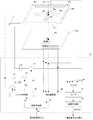
マルチタッチパネル装置1は、使用者からの接触入力を受ける入力面を備えたタッチパネル10と、タッチパネル10を駆動するためのパネル制御部11とを含む。タッチパネル10は、入力面を、液晶ディスプレイなどの表示部に重ね合わせて配置されることによって、使用者に、表示部に仮想的に表示されたボタンなどを感覚的に操作させることができる。 The
タッチパネル10は、スペーサなどにより間隔をおき、互いに対向して設けられた上部基板10b、及び下部基板10aを含む。上部基板10b、及び下部基板10aは、実質的に同一の大きさで、矩形状の入力面を有している。 The
下部基板10aは、ガラス基板の一面に透明導電膜を形成したものである。透明導電膜は、ITO(Indium Tin Oxide)、ZnO(酸化亜鉛)にAl、もしくはGaなどを添加した材料、または、SnO2(酸化スズ)にSbなどが添加された材料などにより構成されている。The
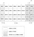
下部基板10aの透明導電膜は、図2に示されるように、接触入力を受ける入力面が複数の領域(1)〜(32)101に分割されている。複数の領域101は、互いに絶縁されるように形成され、例えば、下部基板10aに延設されたフレキシブル基板の配線を介して、個別にパネル制御部11と電気的に接続されている。 As shown in FIG. 2, the transparent conductive film of the
したがって、タッチパネル装置10は、複数の領域101のそれぞれについて、個別に接触入力を検出し、これにより、同時に複数の接触入力を検出することができる。なお、本実施形態では、縦方向で4分割し、横方向で8分割して得た32個の領域101の例を挙げているが、分割の形態は限定されない。また、本実施形態において、各領域101はマトリックス状に配置されているが、配置形態も限定されるものではない。 Therefore, the
一方、上部基板10bは、フィルムの一面に透明な抵抗膜を形成したものである。この抵抗膜は、上記の透明導電膜と同様の材料により形成することができる。また、フィルムは、ポリエチレンテレフタレート、ポリカーボネイト、または透明な樹脂系の材料により構成されている。 On the other hand, the
上部基板10bは、図3に示されるように、対向する一対の辺に沿って2組の電極301,302,311,312が設けられている。この2組の電極301,302,311,312は、例えば、上部基板10bに延設されたフレキシブル基板の配線を介して、パネル制御部11と電気的に接続されている。なお、本実施形態において、タッチパネル10は、抵抗膜方式のものが例示されているが、これに限定されるものではなく、静電容量方式などの他の方式を採用してもよい。 As shown in FIG. 3, the
図4は、パネル制御部11の機能構成を示している。パネル制御部11は、検出部110と、識別番号付与部111と、位置情報出力部112と、設定記録部113と、信号処理部114とを含む。パネル制御部11は、ハードウェアのみで構成してもよいし、ソフトウェアにより機能するものであってもよい。 FIG. 4 shows a functional configuration of the
検出部110は、接触入力を検出するとともに、当該接触入力の位置を検出する。識別番号付与部111は、検出した接触入力のそれぞれに、コンタクトナンバーなどと称される識別番号を付与する。位置情報出力部112は、接触入力のそれぞれについて、識別番号と、検出した位置を示す位置情報とを、CPU20に出力する。設定記録部113は、検出部110の検出と、位置情報出力部12の位置情報の出力とをそれぞれ制限するための設定情報K1,K2を記録している。信号処理部114は、CPU20から入力された信号を処理し、設定情報K1,K2を変更する。以下に、マルチタッチパネル装置1の構成を詳細に説明する。 The
図5は、検出部110の機能構成を示している。検出部110は、上部基板10bの電極301,302,311,312、及び下部基板10aの導電膜の各領域(1)〜(32)101と接続されている。 FIG. 5 shows a functional configuration of the
検出部110は、電圧源V1,V2と、スイッチ45〜47と、電流検出部42と、スイッチ制御部43と、領域選択部44と、フィルタ48と、アナログ−デジタル変換部41と、座標算出部40とを含む。電圧源V1は、スイッチ46を介して、図示のX軸方向に配置された電極301,302の間に一定の電圧を印加する。電圧源V2は、スイッチ47を介して、図示のY軸方向に配置された電極311,312の間に一定の電圧を印加する。また、X軸方向の一方の電極301は、スイッチ45を介して、電源電圧Vccが与えられる。 The
スイッチ45〜47は、スイッチ制御部43からの制御信号S1〜S3によりオンオフ制御される。なお、上記の電源電圧Vcc、電圧源V1,V2の電圧値は、同一であっても、互いに異なっていてもよい。 The
下部基板10aの導電膜の各領域101は、領域選択部44とフィルタ48とに接続されている。領域選択部44は、複数の領域(1)〜(32)101を順次に選択する。この選択の順序は、制限されない。そして、電流検出部42は、設定記録部113の設定情報K1に従い、領域選択部44により選択された領域101の電流を検出し、検出信号S4をスイッチ制御部43に出力する。 Each
また、アナログ−デジタル変換部41は、フィルタ48を介して、各領域101に接続されるとともに、座標算出部40と接続されている。ここで、アナログ−デジタル変換部41は、電圧のアナログ値をデジタル値に変換し、座標算出部40は、上部基板10bの電位勾配に基づいて、各領域101の電圧値から接触入力のX,Y座標を算出する。 The analog-
検出部110の動作を述べると、スイッチ制御部43は、制御信号S1を出力してスイッチ45をオンにし、電圧Vccを電極301に与える。このとき、接触入力Fがあれば、図示されるように、上部基板10bのP点と下部基板10aのQ点が、押圧のため、互いに接触し、Q点が存在する領域(n)101に電流が流れる。そして、領域選択部44が、領域(n)101を選択すると、電流検出部42は、領域(n)101の電流を検出し、検出信号S4をスイッチ制御部43に出力する。他方、電流が検出されないとき、領域選択部44は他の領域101を選択する。 The operation of the
スイッチ制御部43は、検出信号S4が入力されたことを契機として、制御信号S2,S3を出力することによりスイッチ46,47を交互にオンオフする。すなわち、接触入力Fが検出されたとき、スイッチ制御部43は、スイッチ46をオンするとともに、スイッチ47をオフし、次に、スイッチ46をオフするとともに、スイッチ47をオンする。 The
スイッチ46がオンで、スイッチ47がオフであるとき、X軸方向の電極301,302間に電圧が印加される。このとき、P点と電極301,302の間のシート抵抗30a,30bによる分圧値Vxが、Q点を介してフィルタ48に入力される。そして、分圧値Vxは、フィルタ48によりノイズを除去され、アナログ−デジタル変換部41に入力される。座標算出部40は、デジタル値に変換された分圧値Vxに基づいて、電極301,302間を結ぶX軸方向における接触入力Fの位置P,QのX座標を検出する。 When the
一方、スイッチ46がオフで、スイッチ47がオンであるとき、Y軸方向の電極311,312間に電圧が印加される。このとき、上述した内容と同様に、P点と電極311,312の間のシート抵抗31a,31bによる分圧値Vyが、Q点を介してフィルタ48に入力される。そして、分圧値Vyは、フィルタ48によりノイズを除去され、アナログ−デジタル変換部41に入力される。座標算出部40は、デジタル値に変換された分圧値Vyに基づいて、電極311,312間を結ぶY軸方向における接触入力Fの位置P,QのY座標を検出する。なお、X座標とY座標の検出の順序は限定されない。 On the other hand, when the
このようにして得られた接触入力の位置(Px,Py)は、図4に示された識別番号付与部111に出力される。識別番号付与部111は、接触入力に識別番号を付与する。このとき、付与される識別番号は、検出された接触入力の位置(Px,Py)に基づいて選択される。 The contact input position (Px, Py) obtained in this manner is output to the identification
例えば、識別番号付与部111は、時系列に従い、新規の接触入力に、未割り当ての番号のうち、最も若い番号を与えるとよい。もっとも、時系列で付与する番号の順序は、昇順と降順の何れであってもよい。 For example, the identification
一方、識別番号付与部111は、既存の接触入力に対しては、同じ識別番号を付与する。接触入力が既存か、新規かの判断は、識別番号が付与済みの接触入力の位置(Px,Py)を保持しておき、そのうち、検出された接触入力の位置(Px,Py)に近い一定の範囲内に存在するものの有無に基づいて行われる。 On the other hand, the identification
このように、検出部110によって検出された順に、識別番号を付与することによって、システム制御部2における識別番号の管理が容易になる。なお、さらに管理を容易にするため、特定の接触入力に付与済みの識別番号は、他の接触入力がなくなっても、変化しないようにするとよい。 Thus, by assigning identification numbers in the order detected by the
図4に示される位置情報出力部112は、CPU20に、接触入力の位置(Px,Py)を示す位置情報を出力する。例えば、位置情報出力部112は、メモリなどの記録手段を備え、この記録手段に位置情報を書き込むことによって、位置情報を出力することができる。 The position
設定記録部113は、フラッシュメモリなどの不揮発性の記録手段であって、図4に示された検出部110の設定情報K1と、位置情報出力部112の設定情報K2とが記録されている。また、信号処理部114は、CPU20から入力された信号に基づいて、設定情報K1,K2を変更する。これによると、設定情報K1,K2の内容を、システム制御部2の要求に従って、自在に書き換えることができるとともに、装置の電源の投入時に再設定する手間を省くこともできる。 The setting
設定情報K1は、領域101ごとに、接触入力の有効、または無効を示す情報である。検出部110は、この設定情報K1に従って、接触入力の検出を制限する。例えば、電流検出部42は、領域選択部44により選択された領域101の接触入力が、有効に設定されているときのみ、当該領域101の電流検出を行うようにするとよい。 The setting information K1 is information indicating whether the touch input is valid or invalid for each
図6は、斜線で表わされた領域(A)101aの接触入力を無効に設定し、他方、白塗りで表わされた領域(B)101bの接触入力を有効に設定した例を示している。このような設定は、マルチタッチパネル装置1に重なる表示部が、例えば、領域(A)101aに質問文を表示し、領域(B)101bに、その回答を入力するためのエリアを表示した場合が考えられる。 FIG. 6 shows an example in which the contact input of the area (A) 101a represented by hatching is set to be invalid, and the contact input of the area (B) 101b represented by white paint is set to be valid. Yes. In such a setting, for example, the display unit overlapping the
この場合、電流検出部42は、領域選択部44が領域(A)101aを選択したとき、当該領域(A)101aの電流を検出することはない。したがって、マルチタッチパネル装置1は、領域(A)101aにおける接触入力を検出しない。 In this case, when the
他方の領域(B)101bは、接触入力が有効に設定されているため、領域選択部44が領域(B)101bを選択したとき、当該領域(B)101bの電流を検出する。したがって、マルチタッチパネル装置1は、領域(B)101bにおける接触入力を検出する。 Since the other region (B) 101b is set to be effective for contact input, when the
また、設定情報K2は、領域110ごとに、各接触入力に付与された識別番号に応じて、接触入力の有効、または無効を示す情報である。位置情報出力部112は、設定情報K2に従って、位置情報の出力を制限する。例えば、位置情報出力部112は、有効に設定された領域101、及び識別番号の組み合わせに対応する位置情報を上記の記録手段に記録し、他方、無効に設定された領域101、及び識別番号の組み合わせに対応する位置情報を上記の記録手段に記録しないようにするとよい。 The setting information K2 is information indicating whether the contact input is valid or invalid for each
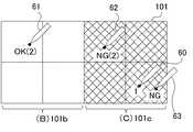
図7は、図6に示された例に追加して、網掛け模様で表わされた領域(C)101cについて、識別番号が「2」以上の接触入力を無効に設定した例を示している。つまり、図7の例は、領域(C)101cにおけるマルチタッチを許容しないように設定したものである。このような設定は、表示部が、例えば、領域(A)101aに説明文を表示し、領域(B)101bに回転操作可能な画像を表示し、さらに、領域(C)101cに、その画像の回転操作の中心として選択可能なエリアを表示した場合が考えられる。 FIG. 7 shows an example in which, in addition to the example shown in FIG. 6, the contact input whose identification number is “2” or more is set to be invalid for the area (C) 101c represented by the shaded pattern. Yes. That is, the example of FIG. 7 is set so as not to allow multi-touch in the region (C) 101c. In such setting, for example, the display unit displays an explanatory text in the area (A) 101a, displays an image that can be rotated in the area (B) 101b, and further displays the image in the area (C) 101c. It is conceivable that a selectable area is displayed as the center of the rotation operation.
この場合、図8に例示されるように、領域(B)101bに識別番号「1」の接触入力60が検出されている状態において(図中の「1」参照)、同じ領域(B)101bへの新規の接触入力61は、識別番号「2」が付与されるから(図中の「(2)」参照)、位置情報出力部112によって出力を制限されることはない。このため、システム制御部2は、接触入力61を検出する(図中の「OK」参照)。 In this case, as illustrated in FIG. 8, in the state where the
また、領域(B)101bに識別番号「1」の接触入力60が検出されている状態において(図中の「1」参照)、領域(C)101cへの新規の接触入力62は、識別番号「2」が付与されるから(図中の「(2)」参照)、位置情報出力部112によって出力を制限される。このため、システム制御部2は、接触入力62を検出しない(図中の「NG」参照)。なお、識別番号「1」の接触入力60と同一の領域101bへの新規の接触入力63は、各領域101に1つの接触入力しか許容されないため、上記の設定によらず、システム制御部2から検出されることはない(図中の「NG」参照)。 In the state where the
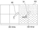
次に、図9に例示されるように、領域(C)101cに識別番号「1」の接触入力60が検出されている状態において(図中の「1」参照)、領域(B)101bへの新規の接触入力61は、識別番号「2」が付与されるから(図中の「(2)」参照)、出力を制限されることない。このため、システム制御部2は、接触入力61を検出する(図中の「OK」参照)。 Next, as illustrated in FIG. 9, in a state where the
また、領域(C)101cに識別番号「1」の接触入力60が検出されている状態において(図中の「1」参照)、同じ領域(C)101cの他領域101への新規の接触入力62は、識別番号「2」が付与されるから(図中の「(2)」参照)、位置情報出力部112によって出力を制限される。このため、システム制御部2は、接触入力62を検出しない(図中の「NG」参照)。なお、識別番号「1」の接触入力60と同一の領域101cへの新規の接触入力63は、各領域101に1つの接触入力しか許容されないため、上記の設定によらず、システム制御部2から検出されることはない(図中の「NG」参照)。 Further, in a state where the
次に、図10は、図7に示された例に追加して、ドット模様で表わされた領域(D)101dについて、識別番号が「1」の接触入力を無効に設定した例を示している。このような設定は、表示部が、例えば、領域(A)101aに説明文を表示し、領域(B)101bに操作可能な画像を表示し、領域(C)101c、及び領域(D)101dに画像操作用のボタンを表示しており、領域(D)101bのボタンが、領域(C)101cのボタンを押した状態でなければ操作可能とならない場合が考えられる。 Next, in addition to the example shown in FIG. 7, FIG. 10 shows an example in which the contact input with the identification number “1” is set to be invalid for the region (D) 101d represented by the dot pattern. ing. In such setting, for example, the display unit displays an explanatory text in the area (A) 101a, displays an operable image in the area (B) 101b, the area (C) 101c, and the area (D) 101d. The button for image operation is displayed on the screen, and the button in the area (D) 101b cannot be operated unless the button in the area (C) 101c is pressed.
この場合、図11に例示されるように、接触入力がない状態において、領域(D)101dへの新規の接触入力60は、識別番号「1」が付与されるから(図中の「(1)」参照)、位置情報出力部112によって出力を制限される。このため、接触入力60は、システム制御部2から検出されることはない(図中の「NG」参照)。 In this case, as illustrated in FIG. 11, in the state where there is no contact input, the
また、図12に例示されるように、領域(B)101bに識別番号「1」の接触入力60が検出されている状態において(図中の「1」参照)、領域(D)101dへの新規の接触入力61は、識別番号「2」が付与されるから(図中の「(2)」参照)、位置情報出力部112によって出力を制限されることはない。このため、システム制御部2は、接触入力61を検出する(図中の「OK」参照)。 Further, as illustrated in FIG. 12, in a state where the
図13は、接触入力がない状態において、領域(B)101bから領域(D)101dに向かって、識別番号「1」の接触入力60を移動させた例を示している(図中の「(1)」参照)。この例において、接触入力60は、領域(B)101bでは、位置情報出力部112によって出力を制限されることはないが、領域(D)101dでは、出力を制限される。このため、システム制御部2は、領域(B)101bにあるときのみ、接触入力60を検出する(図中の「OK」と「NG」参照)。 FIG. 13 shows an example in which the
一方、図14は、図13の例とは逆に、領域(D)101dから領域(B)101bに向かって、識別番号「1」の接触入力60を移動させた例を示している(図中の「(1)」参照)。この例において、接触入力60は、領域(D)101dでは、位置情報出力部112によって出力を制限されるが、領域(B)101bでは、出力を制限されない。このため、システム制御部2は、領域(B)101bにあるときのみ、接触入力60を検出する(図中の「OK」と「NG」参照)。 On the other hand, FIG. 14 shows an example in which the
図13と図14の例において、移動している接触入力60に識別番号「1」が連続的に付与されるのは、上述したように、識別番号付与部111が、接触入力60の位置(Px,Py)の連続性を判断して、同一の識別番号を付与するからである。なお、検出部110は、接触入力60の移動速度より速い速度で全領域101を走査しているため、移動している接触入力60が、誤って、1度に2つ以上の領域101で個別に検出されることはない。 In the example of FIGS. 13 and 14, the identification number “1” is continuously given to the moving
また、図15は、領域(B)101bに識別番号「1」の接触入力60が検出されている状態において(図中の「1」参照)、領域(B)101bから領域(D)101dに向かって、識別番号「2」の接触入力60を移動させた例を示している(図中の「(2)」参照)。この例において、接触入力60は、領域(B)101bと領域(C)101cの両方で、出力を制限されることはない。このため、システム制御部2は、両方の領域101b,101cで接触入力61を検出する(図中の「OK」参照)。 FIG. 15 shows that the
一方、図16は、図15の例とは逆に、領域(B)101bに識別番号「1」の接触入力60が検出されている状態において(図中の「1」参照)、領域(D)101dから領域(B)101bに向かって、識別番号「2」の接触入力60を移動させた例を示している(図中の「(2)」参照)。この例において、接触入力60は、領域(B)101bと領域(C)101cの両方で、出力を制限されることはない。このため、システム制御部2は、両方の領域101b,101cで接触入力61を検出する(図中の「OK」参照)。 On the other hand, in FIG. 16, contrary to the example of FIG. 15, in the state where the
なお、図7、及び図10に例示された設定情報K2は、無効な接触入力の条件として示されているが、これとは逆に、有効な接触入力の条件を示すものであってもよい。つまり、領域(C)の設定は、識別番号「1」の接触入力が有効であるとしてもよいし、また、領域(D)は、識別番号「2」以上の接触入力が有効であるとしてもよい。 The setting information K2 illustrated in FIG. 7 and FIG. 10 is shown as an invalid contact input condition, but on the contrary, it may indicate an effective contact input condition. . That is, the setting of the area (C) may be that the contact input with the identification number “1” is valid, and the area (D) may be valid even if the contact input with the identification number “2” or more is valid. Good.
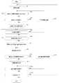
次に、これまで述べたパネル制御部11の動作を、図17に示されたフローを参照して説明する。まず、スイッチ制御部43は、スイッチ45をオンにすることにより電極301に電源電圧Vccを与え、領域選択部44は、1つの領域101を選択する(ステップSt1)。そして、電流検出部42は、設定記録部113の設定情報K1を読み出して、選択された領域101における接触入力が有効、または無効かを判断する(ステップSt2)。 Next, the operation of the
当該領域101における接触入力が無効である場合、電流検出部42は電流検出を行わない(ステップSt2のNO)。このとき、領域選択部44は、全ての領域101の選択が完了していなければ(ステップSt5のNO)、他の領域101を選択して(ステップSt12)、同様のステップSt1,S2を行う。他方、当該領域101における接触入力が有効である場合、電流検出部42は、電流検出により接触入力を検出する(ステップSt2のYES)。電流検出部42は、接触入力を検出すると、検出信号S4をスイッチ制御部43に出力する。 When the contact input in the
スイッチ制御部43は、検出信号S4を受けた場合(ステップSt3のYES)、スイッチ46,47に制御信号S2,S3をそれぞれ出力する。そして、これにより接触入力の座標(Px,Py)が検出される(ステップSt4)。他方、検出信号S4がない場合(ステップSt3のNO)、領域選択部44は、全ての領域101の選択が完了していなければ(ステップSt5のNO)、他の領域101を選択して(ステップSt12)、同様のステップSt2,S3を行う。 When receiving the detection signal S4 (YES in Step St3), the
次に、全ての領域101について上述したステップSt2〜S4が完了すると(ステップSt5のYES)、識別番号付与部111は、検出した各接触入力について、座標(Px,Py)に基づき、新規の接触入力であるか否かを判断する(ステップSt6)。そして、識別番号付与部111は、接触入力が新規である場合(ステップSt6のYES)、この接触入力に識別番号を新規に付与する(ステップSt7)。 Next, when Steps St <b> 2 to S <b> 4 described above are completed for all the regions 101 (YES in Step St <b> 5), the identification
次に、位置情報出力部112は、識別番号を選択して(ステップSt8)、設定記録部113の設定K2を読み出し、選択した識別番号の接触入力が、該当する領域101において有効、または無効かを判断する(ステップSt9)。 Next, the position
そして、位置情報出力部112は、当該接触入力が無効である場合(ステップSt9のNO)、全ての識別番号の選択が完了していなければ(ステップSt11のNO)、他の識別番号を選択して(ステップSt13)、同様のステップSt8、S9を行う。他方、位置情報出力部112は、当該接触入力が有効である場合(ステップSt9のYES)、位置情報をシステム制御部2に出力する(ステップSt10)。 If the contact input is invalid (NO in step St9), the position
全ての識別番号について、同様のステップSt8〜S10が完了すると(ステップSt11のYES)、パネル制御部11は、処理を継続する場合(ステップSt12のNO)、再びステップSt1から処理を行う。他方、パネル制御部11は、例えば、電子機器の電源がオフされたとき、または、システム制御部2からアプリケーションの停止が通知されたとき、処理を終了する(ステップSt12のYES)。なお、このフローにおいて、領域101の選択の順序、及び識別番号の選択の順序に限定はない。 When the same steps St8 to S10 are completed for all the identification numbers (YES in step St11), the
これまで述べたように、検出部110は、複数の領域101のそれぞれに対する個別の設定K1に従って、接触入力の検出を制限するため、システム制御部2に出力される位置情報を、領域101ごとに制限することができる。したがって、システム制御部2は、不要な位置情報の処理が省かれて、位置情報の処理の負荷が低減される。 As described so far, the
一方、タッチパネル装置1は、不要な検出を省くことができるから、消費電力を低減するだけでなく、全体的な検出の処理時間を短縮することもできる。 On the other hand, since the
また、位置情報出力部112は、複数の領域のそれぞれに対する個別の設定K2に従って、位置情報の出力を制限するため、システム制御部2における位置情報の処理の負荷を低減することができる。 Further, since the position
上述した実施形態では、2種類の設定情報K1,K2を併用したが、これに限定されることはなく、何れか一方のみを用いてもよい。この場合、例えば、出力制御部112は、設定情報K1のみを参照して、識別番号によらず、単に領域101ごとに位置情報の出力を制限してもよい。 In the embodiment described above, two types of setting information K1 and K2 are used together, but the present invention is not limited to this, and only one of them may be used. In this case, for example, the
また、上述した実施形態では、設定情報K1,K2を設定記録部113に記録するようにしたが、これに限定されることはない。例えば、システム制御部2に、CPU20がアクセス可能な不揮発性の記録手段を設けておき、CPU20が、直接的に検出部110、及び/または位置情報出力部112に設定情報K1,K2を出力するようにしてもよい。 In the above-described embodiment, the setting information K1 and K2 are recorded in the setting
さらに、設定記録部113に代えて、または設定記録部113とともに、設定情報K1,K2を変更するためのディップスイッチなどの切替手段を設けてもよい。 Further, instead of the setting
以上、好ましい実施例を参照して本発明の内容を具体的に説明したが、本発明の基本的技術思想及び教示に基づいて、当業者であれば、種々の変形態様を採り得ることは自明である。 Although the contents of the present invention have been specifically described above with reference to the preferred embodiments, it is obvious that those skilled in the art can take various modifications based on the basic technical idea and teachings of the present invention. It is.
1 マルチタッチパネル装置
10 タッチパネル
101 領域
110 検出部
111 識別番号付与部
112 位置情報出力部
113 設定記録部
K1,K2 設定情報DESCRIPTION OF
Claims (3)
Translated fromJapanese前記複数の領域のそれぞれについて、個別に前記接触入力の位置を検出する検出部と、
前記検出部により検出された前記接触入力の各々に時系列に従った識別番号を付与する付与部と、
前記接触入力の位置を示す位置情報を出力する位置情報出力部とを備え、
前記位置情報出力部は、前記複数の領域のそれぞれに対して設定される、前記識別番号と前記接触入力の有効無効との関係に従って、前記複数の領域のそれぞれに対応する前記位置情報の出力を制限することを特徴とするマルチタッチパネル装置。A touch panel in which an input surface that receives contact input is divided into a plurality of regions;
For each of the plurality of regions, a detection unit that individually detects the position of the contact input;
An assigning unit that assigns an identification number according to a time series to each of the contact inputs detected by the detecting unit;
A position information output unit that outputs position information indicating the position of the contact input,
The position information output unitis set in pairs to each of the plurality of areasaccording tothe relationship between the effective invalidation of the touch input and the identification number, the output of the positioninformation corresponding to each of the plurality of regions Multi-touch panel device characterized by restricting.
前記複数の領域のそれぞれについて、個別に前記接触入力、及び前記接触入力の位置を検出する検出部と、
前記検出部により検出された前記接触入力の各々に時系列に従った識別番号を付与する付与部と、
前記接触入力の位置を示す位置情報を出力する位置情報出力部とを備え、
前記検出部は、前記複数の領域のそれぞれに対する個別の前記接触入力の有効または無効の設定に従って、前記接触入力の検出を制限し、
前記位置情報出力部は、前記複数の領域のそれぞれに対して設定される、前記識別番号と前記接触入力の有効無効との関係に従って、前記複数の領域のそれぞれに対応する前記位置情報の出力を制限することを特徴とするマルチタッチパネル装置。A touch panel in which an input surface that receives contact input is divided into a plurality of regions;
For each of the plurality of regions, the detection unit that individually detects the contact input and the position of the contact input;
An assigning unit that assigns an identification number according to a time series to each of the contact inputs detected by the detecting unit;
A position information output unit that outputs position information indicating the position of the contact input,
The detection unit limits the detection of the contact input according to the settingof valid or invalid individualcontact input for each of the plurality of regions,
The position information output unitis set in pairs to each of the plurality of areasaccording tothe relationship between the effective invalidation of the touch input and the identification number, the output of the positioninformation corresponding to each of the plurality of regions Multi-touch panel device characterized by restricting.
Priority Applications (1)
| Application Number | Priority Date | Filing Date | Title |
|---|---|---|---|
| JP2011144444AJP5797950B2 (en) | 2011-06-29 | 2011-06-29 | Multi touch panel device |
Applications Claiming Priority (1)
| Application Number | Priority Date | Filing Date | Title |
|---|---|---|---|
| JP2011144444AJP5797950B2 (en) | 2011-06-29 | 2011-06-29 | Multi touch panel device |
Publications (2)
| Publication Number | Publication Date |
|---|---|
| JP2013012046A JP2013012046A (en) | 2013-01-17 |
| JP5797950B2true JP5797950B2 (en) | 2015-10-21 |
Family
ID=47685879
Family Applications (1)
| Application Number | Title | Priority Date | Filing Date |
|---|---|---|---|
| JP2011144444AExpired - Fee RelatedJP5797950B2 (en) | 2011-06-29 | 2011-06-29 | Multi touch panel device |
Country Status (1)
| Country | Link |
|---|---|
| JP (1) | JP5797950B2 (en) |
Families Citing this family (2)
| Publication number | Priority date | Publication date | Assignee | Title |
|---|---|---|---|---|
| JP6309408B2 (en)* | 2014-09-19 | 2018-04-11 | 発紘電機株式会社 | Programmable controller system, programmable display |
| JP6795429B2 (en)* | 2017-03-14 | 2020-12-02 | シャープ株式会社 | Touch-type input device equipped with a touch position recognition circuit and a touch position recognition circuit |
Family Cites Families (5)
| Publication number | Priority date | Publication date | Assignee | Title |
|---|---|---|---|---|
| US6246395B1 (en)* | 1998-12-17 | 2001-06-12 | Hewlett-Packard Company | Palm pressure rejection method and apparatus for touchscreens |
| JP2002287889A (en)* | 2001-03-23 | 2002-10-04 | Sharp Corp | Pen input device |
| JP5241272B2 (en)* | 2008-02-27 | 2013-07-17 | キヤノン株式会社 | Coordinate input device, coordinate input control method, coordinate input control program |
| US8645827B2 (en)* | 2008-03-04 | 2014-02-04 | Apple Inc. | Touch event model |
| KR101534109B1 (en)* | 2008-12-23 | 2015-07-07 | 삼성전자주식회사 | Capacitive touch panel and touch system having the same |
- 2011
- 2011-06-29JPJP2011144444Apatent/JP5797950B2/ennot_activeExpired - Fee Related
Also Published As
| Publication number | Publication date |
|---|---|
| JP2013012046A (en) | 2013-01-17 |
Similar Documents
| Publication | Publication Date | Title |
|---|---|---|
| CN103257769B (en) | A kind of electric capacity In-cell touch panel and display device | |
| US8421772B2 (en) | Resistive touch control device and driving method and driving controller thereof | |
| US9830025B2 (en) | Integrated touch display device for displaying image and performing touch sensing through time-divisional multiplexing | |
| CN104331210B (en) | A kind of In-cell touch panel, its touch control detecting method and display device | |
| KR101454521B1 (en) | Touch detection | |
| KR101521337B1 (en) | Detection of gesture orientation on repositionable touch surface | |
| US20120113071A1 (en) | Input device, coordinates detection method, and program | |
| US8780056B2 (en) | Position detecting device including display function | |
| KR20170002289A (en) | Input with haptic feedback | |
| TW201203071A (en) | Capacitive touchscreen system with multiple drive-sense circuits | |
| CN104407760A (en) | In cell touch panel and display device | |
| CN104182079B (en) | Electronic equipment and position designation method | |
| US20130321291A1 (en) | Electronic apparatus and operating method thereof | |
| CN105637458A (en) | Single layer sensor pattern | |
| JP5008707B2 (en) | Input display board and table | |
| JP6661013B2 (en) | Touch panel control device and electronic equipment | |
| WO2018161547A1 (en) | Touch control substrate and driving method, display panel and display device thereof | |
| US8791922B2 (en) | Resistive touch panel | |
| EP3147764B1 (en) | Touch panel device | |
| JP5797950B2 (en) | Multi touch panel device | |
| US7688313B2 (en) | Touch-sense apparatus available for one-dimensional and two-dimensional modes and control method therefor | |
| US10528178B2 (en) | Capacitive touch sensing with conductivity type determination | |
| CN203217536U (en) | A kind of capacitive built-in touch screen and display device | |
| US20150309622A1 (en) | Active one-layer multi-touch sensor panel device | |
| KR101680256B1 (en) | Touch Screen Panel in Resistive Type |
Legal Events
| Date | Code | Title | Description |
|---|---|---|---|
| A621 | Written request for application examination | Free format text:JAPANESE INTERMEDIATE CODE: A621 Effective date:20140501 | |
| A977 | Report on retrieval | Free format text:JAPANESE INTERMEDIATE CODE: A971007 Effective date:20150213 | |
| A131 | Notification of reasons for refusal | Free format text:JAPANESE INTERMEDIATE CODE: A131 Effective date:20150224 | |
| A521 | Request for written amendment filed | Free format text:JAPANESE INTERMEDIATE CODE: A523 Effective date:20150427 | |
| TRDD | Decision of grant or rejection written | ||
| A01 | Written decision to grant a patent or to grant a registration (utility model) | Free format text:JAPANESE INTERMEDIATE CODE: A01 Effective date:20150818 | |
| A61 | First payment of annual fees (during grant procedure) | Free format text:JAPANESE INTERMEDIATE CODE: A61 Effective date:20150820 | |
| R150 | Certificate of patent or registration of utility model | Ref document number:5797950 Country of ref document:JP Free format text:JAPANESE INTERMEDIATE CODE: R150 | |
| R250 | Receipt of annual fees | Free format text:JAPANESE INTERMEDIATE CODE: R250 | |
| R250 | Receipt of annual fees | Free format text:JAPANESE INTERMEDIATE CODE: R250 | |
| R250 | Receipt of annual fees | Free format text:JAPANESE INTERMEDIATE CODE: R250 | |
| LAPS | Cancellation because of no payment of annual fees |