JP5797932B2 - Semiconductor device - Google Patents
Semiconductor deviceDownload PDFInfo
- Publication number
- JP5797932B2 JP5797932B2JP2011110446AJP2011110446AJP5797932B2JP 5797932 B2JP5797932 B2JP 5797932B2JP 2011110446 AJP2011110446 AJP 2011110446AJP 2011110446 AJP2011110446 AJP 2011110446AJP 5797932 B2JP5797932 B2JP 5797932B2
- Authority
- JP
- Japan
- Prior art keywords
- layer
- insulating layer
- oxide
- transistor
- oxide semiconductor
- Prior art date
- Legal status (The legal status is an assumption and is not a legal conclusion. Google has not performed a legal analysis and makes no representation as to the accuracy of the status listed.)
- Active
Links
Images


Classifications
- H—ELECTRICITY
- H10—SEMICONDUCTOR DEVICES; ELECTRIC SOLID-STATE DEVICES NOT OTHERWISE PROVIDED FOR
- H10D—INORGANIC ELECTRIC SEMICONDUCTOR DEVICES
- H10D30/00—Field-effect transistors [FET]
- H10D30/60—Insulated-gate field-effect transistors [IGFET]
- H10D30/67—Thin-film transistors [TFT]
- H10D30/674—Thin-film transistors [TFT] characterised by the active materials
- H10D30/6755—Oxide semiconductors, e.g. zinc oxide, copper aluminium oxide or cadmium stannate
- H—ELECTRICITY
- H10—SEMICONDUCTOR DEVICES; ELECTRIC SOLID-STATE DEVICES NOT OTHERWISE PROVIDED FOR
- H10D—INORGANIC ELECTRIC SEMICONDUCTOR DEVICES
- H10D30/00—Field-effect transistors [FET]
- H10D30/60—Insulated-gate field-effect transistors [IGFET]
- H10D30/67—Thin-film transistors [TFT]
- H10D30/6704—Thin-film transistors [TFT] having supplementary regions or layers in the thin films or in the insulated bulk substrates for controlling properties of the device
- H—ELECTRICITY
- H10—SEMICONDUCTOR DEVICES; ELECTRIC SOLID-STATE DEVICES NOT OTHERWISE PROVIDED FOR
- H10D—INORGANIC ELECTRIC SEMICONDUCTOR DEVICES
- H10D30/00—Field-effect transistors [FET]
- H10D30/60—Insulated-gate field-effect transistors [IGFET]
- H10D30/67—Thin-film transistors [TFT]
- H10D30/6758—Thin-film transistors [TFT] characterised by the insulating substrates
- H—ELECTRICITY
- H10—SEMICONDUCTOR DEVICES; ELECTRIC SOLID-STATE DEVICES NOT OTHERWISE PROVIDED FOR
- H10D—INORGANIC ELECTRIC SEMICONDUCTOR DEVICES
- H10D86/00—Integrated devices formed in or on insulating or conducting substrates, e.g. formed in silicon-on-insulator [SOI] substrates or on stainless steel or glass substrates
- H10D86/40—Integrated devices formed in or on insulating or conducting substrates, e.g. formed in silicon-on-insulator [SOI] substrates or on stainless steel or glass substrates characterised by multiple TFTs
- H10D86/421—Integrated devices formed in or on insulating or conducting substrates, e.g. formed in silicon-on-insulator [SOI] substrates or on stainless steel or glass substrates characterised by multiple TFTs having a particular composition, shape or crystalline structure of the active layer
- H10D86/423—Integrated devices formed in or on insulating or conducting substrates, e.g. formed in silicon-on-insulator [SOI] substrates or on stainless steel or glass substrates characterised by multiple TFTs having a particular composition, shape or crystalline structure of the active layer comprising semiconductor materials not belonging to the Group IV, e.g. InGaZnO
- H—ELECTRICITY
- H10—SEMICONDUCTOR DEVICES; ELECTRIC SOLID-STATE DEVICES NOT OTHERWISE PROVIDED FOR
- H10D—INORGANIC ELECTRIC SEMICONDUCTOR DEVICES
- H10D86/00—Integrated devices formed in or on insulating or conducting substrates, e.g. formed in silicon-on-insulator [SOI] substrates or on stainless steel or glass substrates
- H10D86/40—Integrated devices formed in or on insulating or conducting substrates, e.g. formed in silicon-on-insulator [SOI] substrates or on stainless steel or glass substrates characterised by multiple TFTs
- H10D86/60—Integrated devices formed in or on insulating or conducting substrates, e.g. formed in silicon-on-insulator [SOI] substrates or on stainless steel or glass substrates characterised by multiple TFTs wherein the TFTs are in active matrices
Landscapes
- Thin Film Transistor (AREA)
- Electroluminescent Light Sources (AREA)
- Devices For Indicating Variable Information By Combining Individual Elements (AREA)
- Liquid Crystal (AREA)
Description
Translated fromJapanese半導体装置に関する。 The present invention relates to a semiconductor device.
なお、本明細書中において半導体装置とは、半導体特性を利用することで機能し得る装置全般をいい、電気光学装置、半導体回路及び電子機器は全て半導体装置である。 Note that in this specification, a semiconductor device refers to all devices that can function by utilizing semiconductor characteristics, and an electro-optical device, a semiconductor circuit, and an electronic device are all semiconductor devices.
絶縁表面を有する基板上に形成された半導体薄膜を用いてトランジスタを構成する技術が注目されている。該トランジスタは集積回路(IC)や画像表示装置(表示装置)のような電子デバイスに広く応用されている。トランジスタに適用可能な半導体薄膜としてシリコン系半導体材料が広く知られているが、その他の材料として酸化物半導体が注目されている。 A technique for forming a transistor using a semiconductor thin film formed over a substrate having an insulating surface has attracted attention. The transistor is widely applied to electronic devices such as an integrated circuit (IC) and an image display device (display device). A silicon-based semiconductor material is widely known as a semiconductor thin film applicable to a transistor, but an oxide semiconductor has attracted attention as another material.
例えば、トランジスタの活性層として、電子キャリア濃度が1018/cm3未満であるインジウム(In)、ガリウム(Ga)、及び亜鉛(Zn)を含む非晶質酸化物を用いたトランジスタが開示されている(特許文献1参照。)。For example, a transistor using an amorphous oxide containing indium (In), gallium (Ga), and zinc (Zn) with an electron carrier concentration of less than 1018 / cm3 is disclosed as an active layer of the transistor. (See Patent Document 1).
酸化物半導体を用いたトランジスタは、アモルファスシリコンを用いたトランジスタよりも動作が速く、多結晶シリコンを用いたトランジスタよりも製造が容易であるものの、電気的特性が変動しやすく信頼性が低いという問題点が知られている。例えば、バイアス−熱ストレス試験(BT試験)前後において、トランジスタのしきい値電圧は変動してしまう。なお、本明細書において、しきい値電圧とは、トランジスタを「オン状態」にするために必要なゲート電圧をいう。そして、ゲート電圧とは、ソースの電位を基準としたゲートの電位との電位差をいう。 A transistor using an oxide semiconductor operates faster than a transistor using amorphous silicon and is easier to manufacture than a transistor using polycrystalline silicon, but its electrical characteristics are likely to change and its reliability is low. The point is known. For example, the threshold voltage of the transistor fluctuates before and after the bias-thermal stress test (BT test). Note that in this specification, the threshold voltage refers to a gate voltage necessary to turn on a transistor. The gate voltage is a potential difference from the gate potential with reference to the source potential.
酸化物半導体を用いたトランジスタのBT試験によるしきい値電圧の変動は、酸化物半導体を用いたトランジスタの信頼性を著しく低下させる。そこで、本発明の一態様は、酸化物半導体を用いた半導体装置の信頼性を向上することを目的とする。 Variation in threshold voltage due to a BT test of a transistor using an oxide semiconductor significantly reduces the reliability of the transistor using an oxide semiconductor. In view of the above, an object of one embodiment of the present invention is to improve the reliability of a semiconductor device including an oxide semiconductor.
本発明の一態様は、酸化物半導体を用いるトランジスタにおいて、酸化物半導体層を介してゲート絶縁層と対向し、かつ酸化物半導体層に少なくとも一部が接する絶縁層として、十分な厚さを有する絶縁層を形成することを技術的思想とする半導体装置または半導体装置の作製方法である。 According to one embodiment of the present invention, a transistor including an oxide semiconductor has a sufficient thickness as an insulating layer which faces the gate insulating layer with the oxide semiconductor layer interposed therebetween and at least part of which is in contact with the oxide semiconductor layer A semiconductor device or a method for manufacturing a semiconductor device, which has a technical idea of forming an insulating layer.
「十分な厚さを有する絶縁層」とは、具体的には、容量換算で、単位面積当たりの容量が2×10⁻⁴F/m2以下、好ましくは1.5×10−4F/m2以下となる厚さを有する絶縁層のことをいう。Specifically, the “insulating layer having a sufficient thickness” means that the capacitance per unit area is 2 × 10⁻⁴ F / m2 or less, preferably 1.5 × 10⁻⁴ F / in, in terms of capacitance. An insulating layer having a thickness of m2 or less.
本発明の一態様は、トップゲート構造の酸化物半導体を用いるトランジスタにおいて、下地絶縁層として、十分な厚さを有する絶縁層を形成することを技術的思想とする半導体装置または半導体装置の作製方法である。 One embodiment of the present invention is a semiconductor device or a method for manufacturing the semiconductor device in which a technical idea is to form an insulating layer having a sufficient thickness as a base insulating layer in a transistor including an oxide semiconductor having a top-gate structure. It is.
十分な厚さを有する下地絶縁層を備えることにより、容量換算で、単位面積当たりの容量が2×10⁻⁴F/m2以下となり、半導体装置の動作などに起因して生じうる電荷などが、基板と下地絶縁層との界面に捕獲される影響を低減することができる。この効果は、基板と下地絶縁層との界面と酸化物半導体層の物理的距離が大きくなることに起因する。By providing the base insulating layer having a sufficient thickness, the capacitance per unit area becomes 2 × 10⁻⁴ F / m2 or less in terms of capacitance, and charges that may be generated due to the operation of the semiconductor device, etc. The influence of being trapped at the interface between the substrate and the base insulating layer can be reduced. This effect results from an increase in the physical distance between the interface between the substrate and the base insulating layer and the oxide semiconductor layer.
上述した基板と下地絶縁層の界面における電荷の捕獲の影響を低減する効果により、酸化物半導体を用いたトランジスタの、BT試験におけるしきい値電圧の変動などの不具合を抑制し、半導体装置の信頼性を向上させることができる。 Due to the effect of reducing the influence of charge trapping at the interface between the substrate and the base insulating layer described above, problems such as threshold voltage fluctuation in a BT test of a transistor using an oxide semiconductor can be suppressed, and the reliability of the semiconductor device can be reduced. Can be improved.
本発明の一態様は、基板と、下地絶縁層と、下地絶縁層上の酸化物半導体層と、酸化物半導体層と電気的に接続するソース電極及びドレイン電極と、酸化物半導体層と一部が接するゲート絶縁層と、ゲート絶縁層上のゲート電極と、を有する半導体装置であり、下地絶縁層は十分な厚さを有することを特徴とする。 One embodiment of the present invention includes a substrate, a base insulating layer, an oxide semiconductor layer over the base insulating layer, a source electrode and a drain electrode that are electrically connected to the oxide semiconductor layer, and part of the oxide semiconductor layer. And a gate electrode over the gate insulating layer, and the base insulating layer has a sufficient thickness.
また、上記構成において、下地絶縁層は、酸化シリコン、酸化窒化シリコン、窒化酸化シリコン、酸化アルミニウムを単層または積層して形成することができる。また、ゲート絶縁層は、酸化シリコン、酸化アルミニウムまたは酸化ハフニウムを単層または積層して形成することができる。なお、基板と下地絶縁層界面の電荷の影響を小さくするという観点から、下地絶縁層は比誘電率の低い材料が好ましい。 In the above structure, the base insulating layer can be formed with a single layer or a stack of silicon oxide, silicon oxynitride, silicon nitride oxide, and aluminum oxide. The gate insulating layer can be formed with a single layer or stacked layers of silicon oxide, aluminum oxide, or hafnium oxide. Note that a material with a low relative dielectric constant is preferable for the base insulating layer from the viewpoint of reducing the influence of electric charges at the interface between the substrate and the base insulating layer.
ここで、酸化窒化シリコンとは、その組成において、窒素よりも酸素の含有量が多いものを示し、例えば、酸素が50原子%以上70原子%以下、窒素が0.5原子%以上15原子%以下、珪素が25原子%以上35原子%以下、水素が0原子%以上10原子%以下の範囲で含まれるものをいう。また、窒化酸化シリコンとは、その組成において、酸素よりも窒素の含有量が多いものを示し、例えば、酸素が5原子%以上30原子%以下、窒素が20原子%以上55原子%以下、珪素が25原子%以上35原子%以下、水素が10原子%以上25原子%以下の範囲で含まれるものをいう。但し、上記範囲は、ラザフォード後方散乱法(RBS:Rutherford Backscattering Spectrometry)や、水素前方散乱法(HFS:Hydrogen Forward scattering Spectrometry)を用いて測定した場合のものである。また、構成元素の含有比率は、その合計が100原子%を超えない値をとる。 Here, silicon oxynitride indicates a composition having a higher oxygen content than nitrogen. For example, oxygen is 50 atomic% to 70 atomic%, and nitrogen is 0.5 atomic% to 15 atomic%. Hereinafter, silicon is contained in the range of 25 atomic% to 35 atomic% and hydrogen in the range of 0 atomic% to 10 atomic%. Silicon nitride oxide refers to a composition having a nitrogen content higher than that of oxygen. For example, oxygen is 5 atomic% to 30 atomic%, nitrogen is 20 atomic% to 55 atomic%, silicon In the range of 25 atomic% to 35 atomic% and hydrogen in the range of 10 atomic% to 25 atomic%. However, the above ranges are those measured using Rutherford Backscattering Spectrometry (RBS) or Hydrogen Forward Scattering Spectrometer (HFS). Further, the content ratio of the constituent elements takes a value that the total does not exceed 100 atomic%.
また、上記構成において、ゲート絶縁層及びゲート電極を覆う保護絶縁層を有することがある。また、酸化物半導体層の下方にバックゲート電極となる導電層を有することがある。 In the above structure, a protective insulating layer that covers the gate insulating layer and the gate electrode may be provided. In addition, a conductive layer serving as a back gate electrode may be provided below the oxide semiconductor layer.
または、本発明の一態様は、ボトムゲート構造の酸化物半導体を用いるトランジスタにおいて、保護絶縁層として、十分な厚さを有する絶縁層を形成することを技術的思想とする半導体装置または半導体装置の作製方法である。 Another embodiment of the present invention is a semiconductor device or a semiconductor device in which a technical idea is to form an insulating layer having a sufficient thickness as a protective insulating layer in a transistor including an oxide semiconductor having a bottom-gate structure. This is a manufacturing method.
十分な厚さを有する保護絶縁層を備えることにより、半導体装置の動作などに起因して生じうる電荷などが、上述の保護絶縁層の表面に捕獲される影響を低減することができる。この効果は、保護絶縁層の表面と酸化物半導体層の物理的距離が大きくなるためである。 By providing the protective insulating layer having a sufficient thickness, it is possible to reduce the influence of charges or the like that can be generated due to the operation of the semiconductor device on the surface of the protective insulating layer. This effect is because the physical distance between the surface of the protective insulating layer and the oxide semiconductor layer is increased.
このように、本発明の一態様による効果は、十分な厚さを有する保護絶縁層に起因するものである。 As described above, the effect of one embodiment of the present invention is attributed to the protective insulating layer having a sufficient thickness.
上述した保護絶縁層の表面における電荷の捕獲の影響を低減する効果により、酸化物半導体を用いたトランジスタのBT試験におけるしきい値電圧の変動などの不具合を抑制し、半導体装置の信頼性を向上させることができる。 By reducing the effect of charge trapping on the surface of the protective insulating layer described above, it is possible to suppress defects such as threshold voltage fluctuations in a BT test of a transistor using an oxide semiconductor, and to improve the reliability of a semiconductor device. Can be made.
本発明の一態様は、下地絶縁層と、下地絶縁層上のゲート電極と、ゲート電極上のゲート絶縁層と、ゲート電極上にゲート絶縁層を介して設けられた酸化物半導体層と、酸化物半導体層と電気的に接続するソース電極及びドレイン電極と、ソース電極及びドレイン電極上に一部が酸化物半導体層と接する保護絶縁層と、を有する半導体装置であり、保護絶縁層は十分な厚さを有することを特徴とする。 One embodiment of the present invention includes a base insulating layer, a gate electrode over the base insulating layer, a gate insulating layer over the gate electrode, an oxide semiconductor layer provided over the gate electrode with the gate insulating layer interposed therebetween, A semiconductor device having a source electrode and a drain electrode electrically connected to the physical semiconductor layer, and a protective insulating layer partly in contact with the oxide semiconductor layer on the source electrode and the drain electrode, the protective insulating layer being sufficient It has a thickness.
また、上記構成において、保護絶縁層は、酸化シリコン、酸化窒化シリコン、窒化酸化シリコン、酸化アルミニウムを単層または積層して形成することができる。また、ゲート絶縁層は、酸化シリコン、酸化アルミニウムまたは酸化ハフニウムを単層または積層して形成することができる。なお、保護絶縁層表面の電荷の影響を小さくするという観点から、保護絶縁層は比誘電率の低い材料が好ましい。 In the above structure, the protective insulating layer can be formed using a single layer or a stacked layer of silicon oxide, silicon oxynitride, silicon nitride oxide, and aluminum oxide. The gate insulating layer can be formed with a single layer or stacked layers of silicon oxide, aluminum oxide, or hafnium oxide. Note that from the viewpoint of reducing the influence of the charge on the surface of the protective insulating layer, the protective insulating layer is preferably made of a material having a low relative dielectric constant.
また、上記構成において、酸化物半導体層の上方にバックゲート電極となる導電層を有することがある。 In the above structure, a conductive layer serving as a back gate electrode may be provided above the oxide semiconductor layer.
なお、上記構成において、ソース電極とドレイン電極の最小の間隔によって決定されるトランジスタのチャネル長Lは、10nm以上10μm以下、例えば、0.1μmから0.5μmとすることができる。もちろん、チャネル長Lは、1μm以上であっても構わない。また、チャネル幅Wについても、10μm以上とすることができる。 Note that in the above structure, the channel length L of the transistor, which is determined by the minimum distance between the source electrode and the drain electrode, can be 10 nm to 10 μm, for example, 0.1 μm to 0.5 μm. Of course, the channel length L may be 1 μm or more. Further, the channel width W can be set to 10 μm or more.
本発明の一態様により、オフ電流が小さく、しきい値電圧のばらつきの少ない、安定した電気特性を有するトランジスタが提供される。 According to one embodiment of the present invention, a transistor having stable electric characteristics with low off-state current and little variation in threshold voltage is provided.
または、本発明の一態様により、電気特性が良好で信頼性の高いトランジスタを有する半導体装置が提供される。 Alternatively, according to one embodiment of the present invention, a semiconductor device including a transistor with favorable electric characteristics and high reliability is provided.
以下では、本発明の実施の形態について図面を用いて詳細に説明する。ただし、本発明は以下の説明に限定されず、その形態及び詳細を様々に変更し得ることは、当業者であれば容易に理解される。また、本発明は以下に示す実施の形態の記載内容に限定して解釈されるものではない。なお、図面を用いて発明の構成を説明するにあたり、同じものを指す符号は異なる図面間でも共通して用いる。なお、同様のものを指す際にはハッチパターンを同じくし、特に符号を付さない場合がある。 Hereinafter, embodiments of the present invention will be described in detail with reference to the drawings. However, the present invention is not limited to the following description, and it is easily understood by those skilled in the art that the modes and details can be variously changed. In addition, the present invention is not construed as being limited to the description of the embodiments below. Note that in describing the structure of the present invention with reference to drawings, the same portions are denoted by the same reference numerals in different drawings. In addition, when referring to the same thing, a hatch pattern is made the same and there is a case where it does not attach a code in particular.
なお、第1、第2として付される序数詞は便宜上用いるものであり、工程順または積層順を示すものではない。また、本明細書において発明を特定するための事項として固有の名称を示すものではない。 The ordinal numbers attached as the first and second are used for convenience and do not indicate the order of steps or the order of lamination. In addition, a specific name is not shown as a matter for specifying the invention in this specification.
(実施の形態1)
本実施の形態では、半導体装置及び半導体装置の作製方法の一形態を、図1乃至図7を用いて説明する。(Embodiment 1)
In this embodiment, one embodiment of a semiconductor device and a method for manufacturing the semiconductor device will be described with reference to FIGS.
図1には、本発明の一態様の半導体装置の例として、トップゲートトップコンタクト型であるトランジスタ151の上面図及び断面図を示す。ここで、図1(A)は上面図であり、図1(B)及び図1(C)はそれぞれ、図1(A)におけるA−B断面及びC−D断面における断面図である。なお、図1(A)では、煩雑になることを避けるため、トランジスタ151の構成要素の一部(例えば、ゲート絶縁層112など)を省略している。 1A and 1B are a top view and a cross-sectional view of a top-gate top-
図1に示すトランジスタ151は、基板100上の、下地絶縁層102、酸化物半導体層106、ソース電極108a、ドレイン電極108b、ゲート絶縁層112、ゲート電極114を含む。 A
下地絶縁層102の材料には、酸化シリコン、酸化窒化シリコンなどを用いればよい。また、下地絶縁層102には、前述の材料と窒化シリコン、窒化酸化シリコン、酸化アルミニウム、窒化アルミニウムまたはこれらの混合材料などを積層して用いてもよい。例えば、下地絶縁層102を窒化シリコン層、窒化酸化シリコン層、酸化アルミニウム層または窒化アルミニウム層と酸化シリコン層の積層構造とすると、基板100などからトランジスタ151への水分の混入を防ぐことができる。下地絶縁層102を積層構造で形成する場合、酸化物半導体層106と接する側を酸化シリコン、酸化窒化シリコンなどの酸化物層とするとよい。なお、下地絶縁層102はトランジスタ151の下地層として機能する。なお、下地絶縁層102は十分な厚さを有することを特徴とする。「十分な厚さを有する絶縁層」とは、容量換算で、単位面積当たりの容量が2×10⁻⁴F/m2以下となる厚さを有する絶縁層をいう。As a material for the
酸化物半導体層に用いる材料としては、四元系金属酸化物であるIn−Sn−Ga−Zn−O系の材料や、三元系金属酸化物であるIn−Ga−Zn−O系の材料、In−Sn−Zn−O系の材料、In−Al−Zn−O系の材料、Sn−Ga−Zn−O系の材料、Al−Ga−Zn−O系の材料、Sn−Al−Zn−O系の材料や、二元系金属酸化物であるIn−Zn−O系の材料、Sn−Zn−O系の材料、Al−Zn−O系の材料、Zn−Mg−O系の材料、Sn−Mg−O系の材料、In−Mg−O系の材料、In−Ga−O系の材料や、In−O系の材料、Sn−O系の材料、Zn−O系の材料などを用いることができる。また、上記の材料にSiO2を含ませてもよい。ここで、例えば、In−Ga−Zn−O系の材料とは、インジウム(In)、ガリウム(Ga)、亜鉛(Zn)を有する酸化物層、という意味であり、その組成比は特に問わない。また、InとGaとZn以外の元素を含んでいてもよい。なお、一例として、In−Zn−O系の材料を用いる場合、原子数比で、In/Zn=0.5以上50以下、好ましくはIn/Zn=1以上20以下、さらに好ましくはIn/Zn=1.5以上15以下とする。Znの原子数比を前述の範囲とすることで、トランジスタの電界効果移動度を向上させることができる。ここで、化合物の原子数比がIn:Zn:O=X:Y:Zのとき、Z>1.5X+Yとすると好ましい。As a material used for the oxide semiconductor layer, an In—Sn—Ga—Zn—O-based material that is a quaternary metal oxide or an In—Ga—Zn—O-based material that is a ternary metal oxide In-Sn-Zn-O-based material, In-Al-Zn-O-based material, Sn-Ga-Zn-O-based material, Al-Ga-Zn-O-based material, Sn-Al-Zn -O-based materials, binary metal oxides In-Zn-O-based materials, Sn-Zn-O-based materials, Al-Zn-O-based materials, Zn-Mg-O-based materials Sn-Mg-O materials, In-Mg-O materials, In-Ga-O materials, In-O materials, Sn-O materials, Zn-O materials, etc. Can be used. Further, the above material may contain SiO2 . Here, for example, an In—Ga—Zn—O-based material means an oxide layer containing indium (In), gallium (Ga), and zinc (Zn), and there is no particular limitation on the composition ratio thereof. . Moreover, elements other than In, Ga, and Zn may be included. Note that when an In—Zn—O-based material is used as an example, the atomic ratio is In / Zn = 0.5 to 50, preferably In / Zn = 1 to 20, and more preferably In / Zn. = 1.5 to 15 By setting the atomic ratio of Zn within the above range, the field effect mobility of the transistor can be improved. Here, when the atomic ratio of the compound is In: Zn: O = X: Y: Z, it is preferable that Z> 1.5X + Y.
また、酸化物半導体層は、化学式InMO3(ZnO)m(m>0)で表記される材料を用いた薄膜により形成することができる。ここで、Mは、Ga、Al、Mn及びCoから選ばれた一または複数の金属元素を示す。例えば、Mとして、Ga、Ga及びAl、Ga及びMnまたはGa及びCoなどを用いることができる。The oxide semiconductor layer can be formed using a thin film formed using a material represented by the chemical formula, InMO3 (ZnO)m (m> 0). Here, M represents one or more metal elements selected from Ga, Al, Mn, and Co. For example, as M, Ga, Ga and Al, Ga and Mn, Ga and Co, or the like can be used.
ゲート絶縁層112は、下地絶縁層102と同様の構成とすることができる。このとき、トランジスタのゲート絶縁層として機能することを考慮して、酸化ハフニウムや酸化アルミニウムなどの比誘電率が高い材料を採用してもよい。また、ゲート耐圧や酸化物半導体層との界面状態などを考慮し、酸化シリコン、酸化窒化シリコン、窒化シリコンに酸化ハフニウムや酸化アルミニウムなどの比誘電率の高い材料を積層してもよい。 The
トランジスタ151上には、さらに保護絶縁層が設けられていてもよい。保護絶縁層は、下地絶縁層102と同様の構成とすることができる。また、ソース電極108aやドレイン電極108bと配線とを電気的に接続させるために、下地絶縁層102、ゲート絶縁層112などには開口が形成されていてもよい。また、酸化物半導体層106の下方に、さらに、第2のゲート電極を有していてもよい。なお、酸化物半導体層106は島状に加工されていることが好ましいが、島状に加工されていなくてもよい。 A protective insulating layer may be further provided over the
図2(A)乃至図2(D)には、トランジスタ151とは異なる構成のトランジスタの断面構造を示す。 2A to 2D illustrate a cross-sectional structure of a transistor having a structure different from that of the
図2(A)に示すトランジスタ152は、下地絶縁層102、酸化物半導体層106、ソース電極108a、ドレイン電極108b、ゲート絶縁層112、ゲート電極114を含む点で、トランジスタ151と共通している。トランジスタ152とトランジスタ151との相違は、酸化物半導体層106と、ソース電極108aやドレイン電極108bが接続する位置である。即ち、トランジスタ152では、酸化物半導体層106の下部において、酸化物半導体層106と、ソース電極108aやドレイン電極108bとが接している。その他の構成要素については、図1のトランジスタ151と同様である。 A
図2(B)に示すトランジスタ153は、下地絶縁層102、酸化物半導体層106、ソース電極108a、ドレイン電極108b、ゲート絶縁層112、ゲート電極114を含む点で、トランジスタ152と共通している。トランジスタ153とトランジスタ152との相違は、酸化物半導体層106に対するゲート電極の位置である。即ち、トランジスタ153では、酸化物半導体層106の下部にゲート絶縁層112を介してゲート電極が設けられている。また、トランジスタ153では、ソース電極108a及びドレイン電極108b及び酸化物半導体層106を覆うように保護絶縁層124が設けられる。その他の構成要素については、図2(A)のトランジスタ152と同様である。 A
図2(C)に示すトランジスタ154は、下地絶縁層102、酸化物半導体層106、ソース電極108a、ドレイン電極108b、ゲート絶縁層112、ゲート電極114を含む点で、トランジスタ151と共通している。トランジスタ154とトランジスタ151との相違は、酸化物半導体層106に対するゲート電極の位置である。即ち、トランジスタ154では、酸化物半導体層106の下部にゲート絶縁層112を介してゲート電極が設けられている。また、トランジスタ154では、ソース電極108a及びドレイン電極108b及び酸化物半導体層106を覆うように保護絶縁層124が設けられる。その他の構成要素については、図1のトランジスタ151と同様である。 A
図2(D)に示すトランジスタ155は、下地絶縁層102、ゲート絶縁層112、ゲート電極114、ソース電極108a、ドレイン電極108bを含む点で、トランジスタ151及びトランジスタ152と共通している。トランジスタ155は、同一平面上の酸化物半導体層中にチャネル領域126、ソース領域122a、ドレイン領域122bを形成する点でトランジスタ151及びトランジスタ152との相違がある。ソース領域122a及びドレイン領域122bには、保護絶縁層124を介して、それぞれソース電極108a及びドレイン電極108bが接続される。なお、図2(D)において、ゲート絶縁層112はゲート電極114の下部にのみ設けられているが、これに限定されない。例えば、チャネル領域126、ソース領域122a、ドレイン領域122bからなる酸化物半導体層を覆うように設けられていても構わない。 A
以下、図3及び図4を用いて、図1に示すトランジスタの作製工程の例について説明する。 Hereinafter, an example of a manufacturing process of the transistor illustrated in FIG. 1 will be described with reference to FIGS.
まず、図3(A)乃至図3(E)を用いて、図1に示すトランジスタ151の作製工程の一例について説明する。 First, an example of a manufacturing process of the
まず、基板100上に下地絶縁層102を形成する(図3(A)参照。)。下地絶縁層102は、容量換算で、単位面積当たりの容量が2×10⁻⁴F/m2以下となる厚さを有することを特徴とする。First, the
基板100の材質などに大きな制限はないが、少なくとも、後の熱処理に耐えうる程度の耐熱性を有している必要がある。例えば、ガラス基板、セラミック基板、石英基板、サファイア基板などを、基板100として用いることができる。また、シリコンや炭化シリコンなどの単結晶半導体基板、多結晶半導体基板、シリコンゲルマニウムなどの化合物半導体基板、SOI基板などを適用することも可能であり、これらの基板上に半導体素子が設けられたものを、基板100として用いてもよい。 There is no particular limitation on the material or the like of the
また、基板100として、可撓性基板を用いてもよい。その場合は、可撓性基板上に直接的にトランジスタを作製する。なお、可撓性基板上にトランジスタを設ける方法としては、基板100として非可撓性のものを用いて、この上にトランジスタを作製した後、トランジスタを剥離し、可撓性基板に転置する方法もある。その場合には、基板100とトランジスタとの間に剥離層を設けるとよい。 Further, a flexible substrate may be used as the
下地絶縁層102の形成方法は、例えば、プラズマCVD法やスパッタリング法などを用いることができる。下地絶縁層102の材料には、酸化シリコン、酸化窒化シリコンなどを用いればよい。また、下地絶縁層102には、前述の材料と窒化シリコン、窒化酸化シリコン、酸化アルミニウム、窒化アルミニウムまたはこれらの混合材料などを積層して用いてもよい。下地絶縁層102を積層構造で形成する場合、酸化物半導体層106と接する側を酸化シリコン、酸化窒化シリコンなどのような酸化物層とするとよい。下地絶縁層102の合計の膜厚は、200nm以上、好ましくは300nm以上とする。下地絶縁層102を厚く形成することにより、基板100と下地絶縁層102の界面からチャネル領域である酸化物半導体層までの物理的な距離が大きくなるため、基板100と下地絶縁層102の界面に捕獲された電荷の影響を低減することができる。 As a formation method of the
例えば、石英(好ましくは合成石英)をターゲットに用い、基板温度30℃以上450℃以下(好ましくは70℃以上200℃以下)、基板とターゲットの間の距離(T−S間距離)を20mm以上400mm以下(好ましくは40mm以上200mm以下)、圧力を0.1Pa以上4Pa以下(好ましくは0.2Pa以上1.2Pa以下)、高周波電源を0.5kW以上12kW以下(好ましくは1kW以上5kW以下)、成膜ガス中のO2/(O2+Ar)割合を1%以上100%以下(好ましくは6%以上100%以下)として、RFスパッタリング法により酸化シリコンを形成する。なお、石英(好ましくは合成石英)ターゲットに代えてシリコンターゲットを用いることもできる。なお、成膜ガスとしては、酸素または、酸素及びアルゴンの混合ガスを用いて行う。For example, quartz (preferably synthetic quartz) is used as a target, the substrate temperature is 30 to 450 ° C. (preferably 70 to 200 ° C.), and the distance between the substrate and the target (T-S distance) is 20 mm or more. 400 mm or less (preferably 40 mm or more and 200 mm or less), a pressure of 0.1 Pa or more and 4 Pa or less (preferably 0.2 Pa or more and 1.2 Pa or less), a high frequency power source of 0.5 kW or more and 12 kW or less (preferably 1 kW or more and 5 kW or less), Silicon oxide is formed by an RF sputtering method with an O2 / (O2 + Ar) ratio in the deposition gas of 1% to 100% (preferably 6% to 100%). Note that a silicon target may be used instead of the quartz (preferably synthetic quartz) target. Note that oxygen or a mixed gas of oxygen and argon is used as a deposition gas.
次に、下地絶縁層102上に酸化物半導体層を形成し、当該酸化物半導体層を加工して島状の酸化物半導体層106を形成する(図3(B)参照。)。 Next, an oxide semiconductor layer is formed over the
酸化物半導体層は、例えば、スパッタリング法、真空蒸着法、パルスレーザ堆積法、CVD法などを用いて形成することができる。また、酸化物半導体層の厚さは、3nm以上50nm以下とすることが好ましい。酸化物半導体層を厚くしすぎると(例えば、厚さを100nm以上)、短チャネル効果の影響が大きくなり、サイズの小さなトランジスタでノーマリーオンになるおそれがあるためである。ここで、「ノーマリーオン」とは、ゲート電極に電圧を印加しなくてもチャネルが存在し、トランジスタに電流が流れてしまう状態のことである。なお、下地絶縁層102及び酸化物半導体層は、大気に触れさせることなく連続して成膜するのが好ましい。 The oxide semiconductor layer can be formed using, for example, a sputtering method, a vacuum evaporation method, a pulse laser deposition method, a CVD method, or the like. The thickness of the oxide semiconductor layer is preferably 3 nm to 50 nm. This is because if the oxide semiconductor layer is too thick (for example, the thickness is 100 nm or more), the influence of the short channel effect becomes large, and a transistor with a small size may be normally on. Here, “normally on” refers to a state in which a channel exists even if no voltage is applied to the gate electrode, and a current flows through the transistor. Note that the
例えば、酸化物半導体層を、In−Ga−Zn−O系の酸化物ターゲットを用いたスパッタリング法により形成する。 For example, the oxide semiconductor layer is formed by a sputtering method using an In—Ga—Zn—O-based oxide target.
In−Ga−Zn−O系の酸化物ターゲットとしては、例えば、組成比として、In2O3:Ga2O3:ZnO=1:1:1[mol数比]の酸化物ターゲットを用いることができる。なお、ターゲットの材料及び組成を上述したものに限定する必要はない。例えば、In2O3:Ga2O3:ZnO=1:1:2[mol数比]の組成比の酸化物ターゲットを用いることもできる。As the In—Ga—Zn—O-based oxide target, for example, an oxide target having a composition ratio of In2 O3 : Ga2 O3 : ZnO = 1: 1: 1 [molar ratio] is used. Can do. The target material and composition need not be limited to those described above. For example, an oxide target having a composition ratio of In2 O3 : Ga2 O3 : ZnO = 1: 1: 2 [molar ratio] can be used.
酸化物ターゲットの相対密度は、90%以上100%以下、好ましくは95%以上99.9%以下とする。相対密度の高い金属酸化物ターゲットを用いることにより、成膜した酸化物半導体層を緻密な層とすることができるためである。 The relative density of the oxide target is 90% to 100%, preferably 95% to 99.9%. This is because by using a metal oxide target having a high relative density, the formed oxide semiconductor layer can be a dense layer.
成膜は、希ガス雰囲気下、酸素雰囲気下または希ガスと酸素の混合ガス雰囲気下などで行えばよい。また、酸化物半導体層への水素、水、水酸基、水素化物などの混入を防ぐために、水素、水、水酸基、水素化物などの不純物が十分に除去された高純度ガスを用いた雰囲気とすることが好ましい。 The film formation may be performed in a rare gas atmosphere, an oxygen atmosphere, or a mixed gas atmosphere of a rare gas and oxygen. In order to prevent entry of hydrogen, water, hydroxyl, hydride, and the like into the oxide semiconductor layer, the atmosphere should be high-purity gas from which impurities such as hydrogen, water, hydroxyl, hydride are sufficiently removed. Is preferred.
例えば、酸化物半導体層は、次のように形成することができる。 For example, the oxide semiconductor layer can be formed as follows.
成膜条件の一例として、基板とターゲットの間との距離を60mm、圧力を0.4Pa、直流(DC)電源を0.5kW、成膜雰囲気をアルゴンと酸素の混合雰囲気(酸素流量比率33%)とすることができる。なお、パルスDCスパッタリング法を用いると、成膜時に発生する粉状物質(パーティクル、ごみともいう)が軽減でき、厚さの分布も均一となるため好ましい。 As an example of the film formation conditions, the distance between the substrate and the target is 60 mm, the pressure is 0.4 Pa, the direct current (DC) power supply is 0.5 kW, the film formation atmosphere is a mixed atmosphere of argon and oxygen (oxygen flow ratio 33%) ). Note that a pulsed DC sputtering method is preferable because powder substances (also referred to as particles or dust) generated in film formation can be reduced and the thickness can be uniform.
このとき、基板温度を100℃以上450℃以下、好ましくは150℃以上250℃以下とすることで、下地絶縁層102と酸化物半導体層との界面準位を低減することができる。 At this time, by setting the substrate temperature to 100 ° C to 450 ° C, preferably 150 ° C to 250 ° C, the interface state between the base
なお、酸化物半導体層106をスパッタリング法により形成する前には、アルゴンガスを導入してプラズマを発生させる逆スパッタを行い、形成表面(例えば下地絶縁層102の表面)の付着物を除去してもよい。ここで、逆スパッタとは、通常のスパッタリングにおいては、スパッタターゲットにイオンを衝突させるところを、逆に、処理表面にイオンを衝突させることによってその表面を改質する方法のことをいう。処理表面にイオンを衝突させる方法としては、アルゴン雰囲気下で処理表面側に高周波電圧を印加して、被処理物付近にプラズマを生成する方法などがある。なお、アルゴン雰囲気に代えて窒素、ヘリウム、酸素などによる雰囲気を適用してもよい。 Note that before the
酸化物半導体層106の加工は、所望の形状のマスクを酸化物半導体層上に形成した後、当該酸化物半導体層をエッチングすることによって行うことができる。上述のマスクは、フォトリソグラフィなどの方法を用いて形成することができる。または、インクジェット法などの方法を用いてマスクを形成してもよい。 The
なお、酸化物半導体層のエッチングは、ドライエッチングでもウェットエッチングでもよい。もちろん、これらを組み合わせて用いてもよい。 Note that the etching of the oxide semiconductor layer may be dry etching or wet etching. Of course, these may be used in combination.
その後、酸化物半導体層に対して、熱処理(第1の熱処理)を行うことが好ましい。この第1の熱処理によって酸化物半導体層中の、過剰な水素(水や水酸基を含む)を除去し、かつ酸化物半導体層の構造を整えることができる。第1の熱処理の温度は、100℃以上650℃以下または基板の歪み点未満、好ましくは250℃以上600℃以下とする。第1の熱処理の雰囲気は、酸化性ガス雰囲気下、もしくは不活性ガス雰囲気下とする。 After that, heat treatment (first heat treatment) is preferably performed on the oxide semiconductor layer. By this first heat treatment, excess hydrogen (including water and a hydroxyl group) in the oxide semiconductor layer can be removed and the structure of the oxide semiconductor layer can be adjusted. The temperature of the first heat treatment is 100 ° C. or higher and 650 ° C. or lower or lower than the strain point of the substrate, preferably 250 ° C. or higher and 600 ° C. or lower. The atmosphere of the first heat treatment is an oxidizing gas atmosphere or an inert gas atmosphere.
なお、不活性ガス雰囲気とは、窒素または希ガスを主成分とする雰囲気であって、水、水素などが含まれないことが好ましい。例えば、熱処理装置に導入する窒素や、ヘリウム、ネオン、アルゴンなどの希ガスの純度を、6N(99.9999%)以上、好ましくは7N(99.99999%)以上(即ち、不純物濃度が1ppm以下、好ましくは0.1ppm以下)とする。不活性ガス雰囲気とは、不活性ガスを主成分とする雰囲気で、反応性ガスが10ppm未満である雰囲気のことである。 Note that the inert gas atmosphere is an atmosphere containing nitrogen or a rare gas as a main component and preferably does not contain water, hydrogen, or the like. For example, the purity of nitrogen or a rare gas such as helium, neon, or argon introduced into the heat treatment apparatus is 6N (99.9999%) or more, preferably 7N (99.99999%) or more (that is, the impurity concentration is 1 ppm or less). , Preferably 0.1 ppm or less). The inert gas atmosphere is an atmosphere containing an inert gas as a main component and having an amount of reactive gas of less than 10 ppm.
なお、酸化性ガスとは、酸素、オゾンまたは亜酸化窒素などであって、水、水素などが含まれないことが好ましい。例えば、熱処理装置に導入する酸素、オゾン、亜酸化窒素の純度を、6N(99.9999%)以上、好ましくは7N(99.99999%)以上(即ち、不純物濃度が1ppm以下、好ましくは0.1ppm以下)とする。酸化性ガス雰囲気には、酸化性ガスを不活性ガスと混合して用いてもよく、酸化性ガスが少なくとも10ppm以上含まれるものとする。 Note that the oxidizing gas is oxygen, ozone, nitrous oxide, or the like, and preferably does not contain water, hydrogen, or the like. For example, the purity of oxygen, ozone, and nitrous oxide introduced into the heat treatment apparatus is 6N (99.9999%) or more, preferably 7N (99.99999%) or more (that is, the impurity concentration is 1 ppm or less, preferably 0. 1 ppm or less). The oxidizing gas atmosphere may be used by mixing an oxidizing gas with an inert gas and contains at least 10 ppm of oxidizing gas.
この第1の熱処理によって、下地絶縁層102と酸化物半導体層106との界面準位を低減することができる。上記界面準位の低減により、BT試験前後のしきい値電圧変動を小さくすることができる。 By this first heat treatment, the interface state between the base
熱処理は、例えば、抵抗発熱体などを用いた電気炉に被処理物を導入し、窒素雰囲気下で、350℃、1時間の条件で行うことができる。この間、酸化物半導体層は大気に触れさせず、水や水素の混入が生じないようにする。 The heat treatment can be performed, for example, by introducing an object to be processed into an electric furnace using a resistance heating element and the like at 350 ° C. for one hour in a nitrogen atmosphere. During this time, the oxide semiconductor layer is not exposed to the air so that water and hydrogen are not mixed.
熱処理装置は電気炉に限られず、加熱されたガスなどの媒体からの熱伝導または熱輻射によって、被処理物を加熱する装置を用いてもよい。例えば、GRTA(Gas Rapid Thermal Anneal)装置、LRTA(Lamp Rapid Thermal Anneal)装置などのRTA(Rapid Thermal Anneal)装置を用いることができる。LRTA装置は、ハロゲンランプ、メタルハライドランプ、キセノンアークランプ、カーボンアークランプ、高圧ナトリウムランプ、高圧水銀ランプなどのランプから発する光(電磁波)の輻射により、被処理物を加熱する装置である。GRTA装置は、高温のガスを用いて熱処理を行う装置である。ガスとしては、アルゴンなどの希ガスまたは窒素のような、熱処理によって被処理物と反応しない不活性ガスが用いられる。 The heat treatment apparatus is not limited to an electric furnace, and an apparatus for heating an object to be processed by heat conduction or heat radiation from a medium such as a heated gas may be used. For example, a rapid thermal annealing (RTA) device such as a GRTA (Gas Rapid Thermal Anneal) device or an LRTA (Lamp Rapid Thermal Anneal) device can be used. The LRTA apparatus is an apparatus that heats an object to be processed by radiation of light (electromagnetic waves) emitted from a lamp such as a halogen lamp, a metal halide lamp, a xenon arc lamp, a carbon arc lamp, a high pressure sodium lamp, or a high pressure mercury lamp. The GRTA apparatus is an apparatus that performs heat treatment using a high-temperature gas. As the gas, an inert gas that does not react with an object to be processed by heat treatment, such as nitrogen or a rare gas such as argon, is used.
例えば、第1の熱処理として、熱せられた不活性ガス雰囲気中に被処理物を投入し、数分間熱した後、当該不活性ガス雰囲気から被処理物を取り出すGRTA処理を行ってもよい。GRTA処理を用いると短時間での高温熱処理が可能となる。また、被処理物の耐熱温度を超える温度条件であっても適用が可能となる。なお、処理中に、不活性ガス雰囲気を、酸化性ガスを含む雰囲気に切り替えてもよい。酸化性ガスを含む雰囲気において第1の熱処理を行うことで、酸化物半導体層106中の酸素欠損を埋めることができるとともに、酸素欠損に起因するエネルギーギャップ中の欠陥準位を低減することができるためである。 For example, as the first heat treatment, a GRTA process may be performed in which an object to be processed is put in a heated inert gas atmosphere and heated for several minutes, and then the object to be processed is extracted from the inert gas atmosphere. When GRTA treatment is used, high-temperature heat treatment can be performed in a short time. In addition, application is possible even under temperature conditions exceeding the heat resistance temperature of the object to be processed. Note that the inert gas atmosphere may be switched to an atmosphere containing an oxidizing gas during the treatment. By performing the first heat treatment in an atmosphere containing an oxidizing gas, oxygen vacancies in the
ところで、上述の熱処理(第1の熱処理)には水素や水などを除去する効果があるため、当該熱処理を、脱水化処理や、脱水素化処理などと呼ぶこともできる。当該脱水化処理、脱水素化処理は、例えば、酸化物半導体層を島状に加工した後などのタイミングにおいて行うことが可能である。また、このような脱水化処理及び脱水素化処理は、一回に限らず複数回行ってもよい。 By the way, since the above heat treatment (first heat treatment) has an effect of removing hydrogen, water, and the like, the heat treatment can be referred to as dehydration treatment, dehydrogenation treatment, or the like. The dehydration treatment and dehydrogenation treatment can be performed, for example, at a timing after the oxide semiconductor layer is processed into an island shape. Further, such dehydration treatment and dehydrogenation treatment are not limited to one time and may be performed a plurality of times.
なお、ここでは、酸化物半導体層106を島状に加工した後に、第1の熱処理を行う構成について説明したが、これに限定されず、第1の熱処理を行った後に、酸化物半導体層106を加工してもよい。 Note that here, the structure in which the first heat treatment is performed after the
次いで、下地絶縁層102及び酸化物半導体層106上に、ソース電極及びドレイン電極(同じ層で形成される配線を含む)を形成するための導電層を形成し、当該導電層を加工して、ソース電極108a及びドレイン電極108bを形成する(図3(C)参照。)。なお、ここで形成されるソース電極108aの端部とドレイン電極108bの端部との最小の間隔によって、トランジスタのチャネル長Lが決定されることになる。 Next, a conductive layer for forming a source electrode and a drain electrode (including a wiring formed using the same layer) is formed over the
ソース電極108a及びドレイン電極108bに用いる導電層としては、例えば、Al、Cr、Cu、Ta、Ti、Mo、Wから選ばれた元素を含む金属層または上述した元素を成分とする金属窒化物層(窒化チタン層、窒化モリブデン層、窒化タングステン層)などを用いることができる。また、Al、Cuなどの低融点かつ低抵抗の金属層の下側及び上側の一方または双方に、Ti、Mo、Wなどの高融点金属層またはこれらの金属窒化物層(窒化チタン層、窒化モリブデン層、窒化タングステン層)を積層させた構成を用いてもよい。 As the conductive layer used for the
また、ソース電極108a及びドレイン電極108bに用いる導電層は、導電性の金属酸化物で形成してもよい。導電性の金属酸化物としては酸化インジウム(In2O3等)、酸化スズ(SnO2等)、酸化亜鉛(ZnO等)、酸化インジウム酸化スズ合金(In2O3―SnO2等、ITOと略記する)、酸化インジウム酸化亜鉛合金(In2O3―ZnO等)またはこれらの金属酸化物材料に酸化シリコンを含ませたものを用いることができる。The conductive layer used for the
導電層の加工は、レジストマスクを用いたエッチングによって行うことができる。当該エッチングに用いるレジストマスク形成時の露光には、紫外線やKrFレーザ光やArFレーザ光などを用いるとよい。 The conductive layer can be processed by etching using a resist mask. Ultraviolet light, KrF laser light, ArF laser light, or the like is preferably used for light exposure for forming the resist mask used for the etching.
なお、チャネル長L=25nm未満となるように露光を行う場合には、例えば、数nm〜数10nmと極めて波長が短い超紫外線(Extreme Ultraviolet)を用いて、レジストマスク形成時の露光を行うとよい。超紫外線による露光は、解像度が高く焦点深度も大きい。したがって、後に形成されるトランジスタのチャネル長Lを短くすることが可能であり、回路の動作を速くすることができる。 Note that when exposure is performed so that the channel length L is less than 25 nm, for example, exposure at the time of resist mask formation is performed using extreme ultraviolet (Extreme Ultraviolet) having an extremely short wavelength of several nm to several tens of nm. Good. Exposure by extreme ultraviolet light has a high resolution and a large depth of focus. Accordingly, the channel length L of a transistor to be formed later can be shortened, and the circuit can be operated quickly.
また、いわゆる多階調マスクによって形成されたレジストマスクを用いてエッチングを行ってもよい。多階調マスクを用いて形成されたレジストマスクは、複数の厚さを有する形状となり、アッシングによってさらに形状を変形させることができるため、異なるパターンに加工する複数のエッチング工程に用いることが可能である。このため、一枚の多階調マスクによって、少なくとも二種類以上の異なるパターンに対応するレジストマスクを形成することができる。つまり、工程の簡略化が可能となる。 Further, etching may be performed using a resist mask formed by a so-called multi-tone mask. A resist mask formed using a multi-tone mask has a shape with a plurality of thicknesses, and the shape can be further deformed by ashing. Therefore, the resist mask can be used for a plurality of etching processes to be processed into different patterns. is there. Therefore, a resist mask corresponding to at least two kinds of different patterns can be formed with one multi-tone mask. That is, the process can be simplified.
なお、導電層のエッチングの際に、酸化物半導体層106の一部がエッチングされ、溝部(凹部)を有する酸化物半導体層となることもある。 Note that when the conductive layer is etched, part of the
その後、酸素、オゾン、亜酸化窒素などのガスを用いたプラズマ処理を行い、露出している酸化物半導体層106の表面を酸化し、酸素欠損を埋めてもよい。プラズマ処理を行った場合、当該プラズマ処理に続けて大気に触れさせることなく、酸化物半導体層106の一部に接するゲート絶縁層112を形成することが好ましい。 After that, plasma treatment using a gas such as oxygen, ozone, or nitrous oxide may be performed to oxidize the exposed surface of the
次に、ソース電極108a及びドレイン電極108bを覆い、かつ、酸化物半導体層106の一部と接するように、ゲート絶縁層112を形成する(図3(D)参照。)。 Next, the
ゲート絶縁層112は、下地絶縁層102と同様の構成とすることができる。ただし、トランジスタのゲート絶縁層として機能することを考慮して、酸化ハフニウムや酸化アルミニウムなどの比誘電率が高い材料を採用してもよい。また、ゲート耐圧や酸化物半導体層との界面状態などを考慮し、酸化シリコン、酸化窒化シリコン、窒化シリコンに酸化ハフニウムや酸化アルミニウムなどの比誘電率の高い材料を積層して用いてもよい。ゲート絶縁層112の合計の膜厚は、好ましくは1nm以上300nm以下、より好ましくは5nm以上50nm以下とする。ゲート絶縁層が厚いほど短チャネル効果が顕著となり、しきい値電圧が負方向へシフトしやすい傾向となる。また、ゲート絶縁層が5nm以下となるとトンネル電流によるリークが増大することがわかっている。 The
ゲート絶縁層112の形成後には、第2の熱処理を行うのが好ましい。第2の熱処理の温度は、250℃以上700℃以下、好ましくは350℃以上600℃以下または基板の歪み点未満とする。 After the
第2の熱処理は、酸化性ガス雰囲気下または不活性ガス雰囲気下で行えばよいが、雰囲気中に水、水素などが含まれないことが好ましい。また、熱処理装置に導入するガスの純度を、6N(99.9999%)以上好ましくは7N(99.99999%)以上(即ち不純物濃度を1ppm以下、好ましくは0.1ppm以下)とすることが好ましい。 The second heat treatment may be performed in an oxidizing gas atmosphere or an inert gas atmosphere, but it is preferable that water, hydrogen, and the like be not contained in the atmosphere. The purity of the gas introduced into the heat treatment apparatus is preferably 6N (99.9999%) or more, preferably 7N (99.9999999%) or more (that is, the impurity concentration is 1 ppm or less, preferably 0.1 ppm or less). .
第2の熱処理においては、酸化物半導体層とゲート絶縁層112の界面準位を低減することができる。また、同時にゲート絶縁層112中の欠陥も低減することができる。 In the second heat treatment, the interface state between the oxide semiconductor layer and the
なお、第2の熱処理のタイミングは、ゲート絶縁層112の形成後であれば特に限定されない。例えば、ゲート電極114の形成後に第2の熱処理を行ってもよい。 Note that there is no particular limitation on the timing of the second heat treatment as long as it is after the
その後、ゲート電極114を形成する(図3(E)参照。)。ゲート電極114は、モリブデン、チタン、タンタル、タングステン、アルミニウム、銅、ネオジム、スカンジウムなどの金属材料、これらの窒化物、またはこれらを主成分とする合金材料を用いて形成することができる。なお、ゲート電極114は、単層構造としてもよいし、積層構造としてもよい。 After that, the
以上の工程でトランジスタ151が作製される。 Through the above process, the
次に、図4(A)乃至図4(E)を用いて、図2(A)に示すトランジスタ152の作製工程の一例について説明する。 Next, an example of a manufacturing process of the
まず、基板100上に下地絶縁層102を形成する(図4(A)参照。)。下地絶縁層102はトランジスタ151と同様に、容量換算で、単位面積当たりの容量が2×10⁻⁴F/m2以下、好ましくは1.5×10−4F/m2以下となる厚さを有することを特徴とする。First, the
次に、下地絶縁層102上に、ソース電極及びドレイン電極(これと同じ層で形成される配線を含む)を形成するための導電層を形成し、当該導電層を加工して、ソース電極108a及びドレイン電極108bを形成する(図4(B)参照。)。 Next, a conductive layer for forming a source electrode and a drain electrode (including a wiring formed using the same layer) is formed over the
次に、下地絶縁層102上に、ソース電極108a及びドレイン電極108bと接続する酸化物半導体層を形成し、当該酸化物半導体層を加工して島状の酸化物半導体層106を形成する(図4(C)参照。)。その後、トランジスタ151と同様の第1の熱処理を行ってもよい。 Next, an oxide semiconductor layer connected to the
次に、ソース電極108a及びドレイン電極108b、酸化物半導体層106を覆い、かつ、酸化物半導体層106、ソース電極108a及びドレイン電極108bの一部と接するように、ゲート絶縁層112を形成する(図4(D)参照。)。その後、トランジスタ151と同様に第2の熱処理を行ってもよい。 Next, the
その後、ゲート電極114を形成する(図4(E)参照。)。 After that, the
以上の工程でトランジスタ152が形成される。 Through the above process, the
なお、基板と下地絶縁層の界面に電荷がトラップされると、トランジスタのしきい値電圧はシフトする。例えば、正電荷がトラップされると、トランジスタのしきい値電圧は負方向にシフトする。このような電荷捕獲の要因の一つとして、陽イオン(またはその原因たる原子)の移動及びトラップのモデルを仮定することができる。本発明の一態様では、容量換算で、単位面積当たりの容量が2×10⁻⁴F/m2以下、好ましくは1.5×10−4F/m2以下となる厚さを有する下地絶縁層を用い、基板と下地絶縁層の界面からの物理的な距離を大きくすることで、基板と下地絶縁層の界面からの影響を低減することができ、トランジスタのしきい値電圧のシフトを抑制することができる。Note that when charge is trapped at the interface between the substrate and the base insulating layer, the threshold voltage of the transistor shifts. For example, when a positive charge is trapped, the threshold voltage of the transistor shifts in the negative direction. One such charge trapping factor can be assumed to be a model of cation (or atom responsible) migration and trapping. In one embodiment of the present invention, the base insulating layer has a thickness with which the capacitance per unit area is 2 × 10⁻⁴ F / m2 or less, preferably 1.5 × 10⁻⁴ F / m2 or less, in terms of capacitance. By using a layer and increasing the physical distance from the interface between the substrate and the base insulating layer, the influence from the interface between the substrate and the base insulating layer can be reduced, and the threshold voltage shift of the transistor is suppressed. can do.
次に、図5(A)乃至図5(E)を用いて、図2(B)に示すトランジスタ153の作製工程の一例について説明する。 Next, an example of a manufacturing process of the
まず、基板100上に下地絶縁層102を形成する(図5(A)参照。)。 First, the
次に、下地絶縁層102上に、ゲート電極114を形成する(図5(B)参照。)。 Next, the
次に、ゲート電極114上に、ゲート絶縁層112を形成する(図5(C)参照。)。 Next, the
次に、ゲート絶縁層112上に、ソース電極108a及びドレイン電極108bを形成し、ソース電極108a及びドレイン電極108bと接続する酸化物半導体層を形成し、当該酸化物半導体層を加工して島状の酸化物半導体層106を形成する(図5(D)参照。)。その後、トランジスタ151と同様の第1の熱処理を行ってもよい。 Next, the
次に、酸化物半導体層106及びソース電極108a及びドレイン電極108bを覆うように保護絶縁層124を形成する(図5(E)参照。)。保護絶縁層は、トランジスタ151における下地絶縁層と同様に、容量換算で、単位面積当たりの容量が2×10⁻⁴F/m2以下、好ましくは1.5×10−4F/m2以下となる厚さを有することを特徴とする。その後、トランジスタ151と同様に第2の熱処理を行ってもよい。Next, the protective insulating
以上の工程でトランジスタ153が形成される。 Through the above process, the
次に、図6(A)乃至図6(E)を用いて、図2(C)に示すトランジスタ154の作製工程の一例について説明する。 Next, an example of a manufacturing process of the
まず、基板100上に下地絶縁層102を形成する(図6(A)参照。)。 First, the
次に、下地絶縁層102上に、ゲート電極114を形成する(図6(B)参照。)。 Next, the
次に、ゲート電極114上に、ゲート絶縁層112を形成する(図6(C)参照。)。 Next, the
次に、ゲート絶縁層112上に、酸化物半導体層を形成し、当該酸化物半導体層を加工して島状の酸化物半導体層106を形成する。その後、トランジスタ151と同様の第1の熱処理を行ってもよい。その後、酸化物半導体層106に接続するようにソース電極108a及びドレイン電極108bを形成する(図6(D)参照。)。 Next, an oxide semiconductor layer is formed over the
次に、酸化物半導体層106及びソース電極108a及びドレイン電極108bを覆うように保護絶縁層124を形成する(図6(E)参照。)。保護絶縁層は、トランジスタ151における下地絶縁層と同様に、容量換算で、単位面積当たりの容量が2×10⁻⁴F/m2以下、好ましくは1.5×10−4F/m2以下となる厚さを有することを特徴とする。その後、トランジスタ151と同様に第2の熱処理を行ってもよい。Next, the protective insulating
以上の工程でトランジスタ154が形成される。 Through the above process, the
図7(A)乃至図7(E)を用いて、図2(D)に示すトランジスタ155の作製工程の一例について説明する。 An example of a manufacturing process of the
まず、基板100上に下地絶縁層102を形成する(図7(A)参照。)。下地絶縁層102は容量換算で、単位面積当たりの容量が2×10⁻⁴F/m2以下、好ましくは1.5×10−4F/m2以下となる厚さを有することを特徴とする。First, the
次に、下地絶縁層102上に、酸化物半導体層を形成し、当該酸化物半導体層を加工して島状の酸化物半導体層106を形成する(図7(B)参照。)。その後、トランジスタ151と同様の第1の熱処理を行ってもよい。 Next, an oxide semiconductor layer is formed over the
次に、ゲート絶縁層112及びゲート電極114を形成し、フォトリソグラフィにより同様のパターンに加工する(図7(C)参照。)。このとき、ゲート電極114を加工し、その後、ゲート電極114をマスクにゲート絶縁層112を加工してもよい。 Next, the
次に、ゲート電極114をマスクに用いて酸化物半導体層106を低抵抗化し、ソース領域122a及びドレイン領域122bを形成する。低抵抗化されないゲート電極下の領域はチャネル領域126となる(図7(D)参照。)。低抵抗化の方法としては、アルゴンプラズマ処理、水素プラズマ処理またはアンモニアプラズマ処理などが挙げられる。このとき、ゲート電極の幅によってトランジスタのチャネル長Lが決定されることになる。このように、ゲート電極をマスクに用いてパターニングすることで、ゲート電極とソース領域、ドレイン領域の重なりが生じず、この領域における寄生容量が生じないため、トランジスタ動作を速くすることができる。 Next, the resistance of the
次に、保護絶縁層124を形成し、ソース領域122a及びドレイン領域122bと重畳する部分の保護絶縁層124に開口部を設ける。ソース電極及びドレイン電極(これと同じ層で形成される配線を含む)を形成するための導電層を形成し、当該導電層を加工して、ソース電極108a及びドレイン電極108bを形成する(図7(E)参照。)。 Next, the protective insulating
以上の工程でトランジスタ155が作製される。 Through the above process, the
以上のように、安定した電気的特性を有する酸化物半導体を用いた半導体装置を提供することができる。よって、信頼性の高い半導体装置を提供することができる。 As described above, a semiconductor device including an oxide semiconductor having stable electrical characteristics can be provided. Therefore, a highly reliable semiconductor device can be provided.
以上、本実施の形態に示す構成、方法などは、他の実施の形態に示す構成、方法などと適宜組み合わせて用いることができる。 The structures, methods, and the like described in this embodiment can be combined as appropriate with any of the structures, methods, and the like described in the other embodiments.
(実施の形態2)
実施の形態1で例示したトランジスタを用いて表示機能を有する半導体装置(表示装置ともいう)を作製することができる。また、トランジスタを含む駆動回路の一部または全体を、画素部と同じ基板上に一体形成し、システムオンパネルを形成することができる。(Embodiment 2)
A semiconductor device (also referred to as a display device) having a display function can be manufactured using the transistor exemplified in Embodiment 1. In addition, part or the whole of a driver circuit including a transistor can be formed over the same substrate as the pixel portion to form a system-on-panel.
図8(A)において、第1の基板201上に設けられた画素部202を囲むようにして、シール材205が設けられ、第2の基板206によって封止されている。図8(A)においては、第1の基板201上のシール材205によって囲まれている領域とは異なる領域に、別途用意された基板上に単結晶半導体層または多結晶半導体層で形成された走査線駆動回路204、信号線駆動回路203が実装されている。また別途形成された信号線駆動回路203と、走査線駆動回路204または画素部202に与えられる各種信号及び電位は、FPC(Flexible printed circuit)218a、218bから供給されている。 In FIG. 8A, a
図8(B)及び図8(C)において、第1の基板201上に設けられた画素部202と、走査線駆動回路204とを囲むようにして、シール材205が設けられている。また画素部202と、走査線駆動回路204の上に第2の基板206が設けられている。よって画素部202と、走査線駆動回路204とは、第1の基板201とシール材205と第2の基板206とによって、表示素子と共に封止されている。図8(B)及び図8(C)においては、第1の基板201上のシール材205によって囲まれている領域とは異なる領域に、別途用意された基板上に単結晶半導体層または多結晶半導体層で形成された信号線駆動回路203が実装されている。図8(B)及び図8(C)においては、別途形成された信号線駆動回路203と、走査線駆動回路204または画素部202に与えられる各種信号及び電位は、FPC218から供給されている。 8B and 8C, a
また図8(B)及び図8(C)においては、信号線駆動回路203を別途形成し、第1の基板201に実装している例を示しているが、この構成に限定されない。走査線駆動回路を別途形成して実装してもよいし、信号線駆動回路の一部または走査線駆動回路の一部のみを別途形成して実装してもよい。 8B and 8C illustrate an example in which the signal
なお、別途形成した駆動回路の接続方法は、特に限定されるものではなく、COG(Chip On Glass)方法、ワイヤボンディング方法、或いはTAB(Tape Automated Bonding)方法などを用いることができる。図8(A)は、COG方法により信号線駆動回路203、走査線駆動回路204を実装する例であり、図8(B)は、COG方法により信号線駆動回路203を実装する例であり、図8(C)は、TAB方法により信号線駆動回路203を実装する例である。 Note that a connection method of a driver circuit which is separately formed is not particularly limited, and a COG (Chip On Glass) method, a wire bonding method, a TAB (Tape Automated Bonding) method, or the like can be used. 8A is an example in which the signal
また、表示装置は、表示素子が封止された状態にあるパネルと、該パネルにコントローラを含むICなどを実装した状態にあるモジュールとを含む。 The display device includes a panel in which the display element is sealed, and a module in which an IC including a controller is mounted on the panel.
なお、本明細書中における表示装置とは、画像表示デバイス、表示デバイス、もしくは光源(照明装置含む)を指す。また、コネクター、例えばFPCもしくはTABテープもしくはTCPが取り付けられたモジュール、TABテープやTCPの先にプリント配線板が設けられたモジュールまたは表示素子にCOG方式によりICが直接実装されたモジュールも全て表示装置に含むものとする。 Note that a display device in this specification means an image display device, a display device, or a light source (including a lighting device). In addition, a display device includes a connector, for example, a module to which an FPC, TAB tape or TCP is attached, a module in which a printed wiring board is provided at the end of a TAB tape or TCP, or a module in which an IC is directly mounted on a display element by a COG method To include.
また第1の基板上に設けられた画素部及び走査線駆動回路は、トランジスタを複数有しており、実施の形態1で一例を示したトランジスタを適用することができる。 The pixel portion and the scan line driver circuit provided over the first substrate include a plurality of transistors, and the transistor described as an example in Embodiment 1 can be used.
表示装置に設けられる表示素子としては液晶素子(液晶表示素子ともいう)、発光素子(発光表示素子ともいう)、を用いることができる。発光素子は、電流または電圧によって輝度が制御される素子をその範疇に含んでおり、具体的には無機EL(Electro Luminescence)素子、有機EL素子などを含む。また、電子インクなど、電気的作用によりコントラストが変化する表示媒体も適用することができる。 As a display element provided in the display device, a liquid crystal element (also referred to as a liquid crystal display element) or a light-emitting element (also referred to as a light-emitting display element) can be used. The light-emitting element includes, in its category, an element whose luminance is controlled by current or voltage. Specifically, the light-emitting element includes an inorganic EL (Electro Luminescence) element, an organic EL element, and the like. In addition, a display medium whose contrast is changed by an electric effect, such as electronic ink, can be used.
半導体装置の一形態について、図9乃至図11を用いて説明する。図9乃至図11は、図8(B)のM−Nにおける断面図に相当する。 One embodiment of a semiconductor device is described with reference to FIGS. 9 to 11 correspond to cross-sectional views taken along line MN in FIG. 8B.
図9乃至図11で示すように、半導体装置は接続端子電極215及び端子電極216を有しており、接続端子電極215及び端子電極216はFPC218が有する端子と異方性導電層219を介して、電気的に接続されている。 9 to 11, the semiconductor device includes a
接続端子電極215は、第1の電極層230と同じ導電層から形成され、端子電極216は、トランジスタ210、トランジスタ211のソース電極及びドレイン電極と同じ導電層で形成されている。 The
また第1の基板201上に設けられた画素部202と、走査線駆動回路204は、トランジスタを複数有しており、図9乃至図11では、画素部202に含まれるトランジスタ210と、走査線駆動回路204に含まれるトランジスタ211とを例示している。 The
本実施の形態では、トランジスタ210、トランジスタ211として、実施の形態1で示したトランジスタを適用することができる。トランジスタ210、トランジスタ211は、電気的特性変動が抑制されており、電気的に安定である。よって、図9乃至図11で示す本実施の形態の半導体装置として信頼性の高い半導体装置を提供することができる。 In this embodiment, the transistor described in Embodiment 1 can be used as the
画素部202に設けられたトランジスタ210は表示素子と電気的に接続し、表示パネルを構成する。表示素子は表示を行うことができれば特に限定されず、様々な表示素子を用いることができる。 The
図9に表示素子として液晶素子を用いた液晶表示装置の例を示す。図9において、表示素子である液晶素子213は、第1の電極層230、第2の電極層231、及び液晶層208を含む。なお、液晶層208を挟持するように配向層として機能する絶縁層232、233が設けられている。第2の電極層231は第2の基板206側に設けられ、第1の電極層230と第2の電極層231とは液晶層208を介して積層する構成となっている。 FIG. 9 shows an example of a liquid crystal display device using a liquid crystal element as a display element. In FIG. 9, a
また、スペーサ235は絶縁層を選択的にエッチングすることで得られる柱状のスペーサであり、液晶層208の厚さ(セルギャップ)を制御するために設けられている。なお球状のスペーサを用いていてもよい。 The
表示素子として、液晶素子を用いる場合、サーモトロピック液晶、低分子液晶、高分子液晶、高分子分散型液晶、強誘電性液晶、反強誘電性液晶などを用いることができる。これらの液晶材料は、条件により、コレステリック相、スメクチック相、キュービック相、カイラルネマチック相、等方相などを示す。When a liquid crystal element is used as the display element, a thermotropic liquid crystal, a low molecular liquid crystal, a polymer liquid crystal, a polymer dispersed liquid crystal, a ferroelectric liquid crystal, an antiferroelectric liquid crystal, or the like can be used. These liquid crystal materials exhibit a cholesteric phase, a smectic phase, a cubic phase, a chiral nematic phase, an isotropic phase, and the like depending on conditions.
また、配向層を不要とすることができるブルー相を示す液晶を用いてもよい。ブルー相は液晶相の一つであり、コレステリック液晶を昇温していくと、コレステリック相から等方相へ転移する直前に発現する相である。ブルー相は狭い温度範囲でしか発現しないため、温度範囲を改善するためにカイラル剤を混合させた液晶組成物を用いて液晶層に用いる。ブルー相を示す液晶とカイラル剤とを含む液晶組成物は、応答速度が1msec以下と短く、光学的等方性であるため配向処理が不要であり、視野角依存性が小さい。また配向層を設けなくてもよいのでラビング処理も不要となるため、ラビング処理によって引き起こされる静電破壊を防止することができ、作製工程中の液晶表示装置の不良や破損を軽減することができる。よって液晶表示装置の生産性を向上させることが可能となる。 Alternatively, a liquid crystal exhibiting a blue phase for which an alignment layer is unnecessary may be used. The blue phase is one of the liquid crystal phases. When the temperature of the cholesteric liquid crystal is increased, the blue phase appears immediately before the transition from the cholesteric phase to the isotropic phase. Since the blue phase appears only in a narrow temperature range, a liquid crystal composition mixed with a chiral agent is used for the liquid crystal layer in order to improve the temperature range. A liquid crystal composition containing a liquid crystal exhibiting a blue phase and a chiral agent has a response speed as short as 1 msec or less and is optically isotropic, so alignment treatment is unnecessary and viewing angle dependence is small. In addition, since an alignment layer is not required, a rubbing process is not required, so that electrostatic breakdown caused by the rubbing process can be prevented, and defects or breakage of the liquid crystal display device during the manufacturing process can be reduced. . Therefore, the productivity of the liquid crystal display device can be improved.
また、液晶材料の固有抵抗率は、1×10⁹Ω・cm以上であり、好ましくは1×10¹¹Ω・cm以上であり、さらに好ましくは1×10¹²Ω・cm以上である。なお、本明細書における固有抵抗率の値は、20℃で測定した値とする。The specific resistivity of the liquid crystal material is 1 × 10⁹ Ω · cm or more, preferably 1 × 10¹¹ Ω · cm or more, and more preferably 1 × 10¹² Ω · cm or more. In addition, the value of the specific resistivity in this specification shall be the value measured at 20 degreeC.
液晶表示装置に設けられる保持容量の大きさは、画素部に配置されるトランジスタのリーク電流などを考慮して、所定の期間の間電荷を保持できるように設定される。高純度の酸化物半導体層を有するトランジスタを用いることにより、各画素における液晶容量に対して1/3以下、好ましくは1/5以下の容量の大きさを有する保持容量を設ければ充分である。 The size of the storage capacitor provided in the liquid crystal display device is set so that charges can be held for a predetermined period in consideration of a leakage current of a transistor arranged in the pixel portion. By using a transistor having a high-purity oxide semiconductor layer, it is sufficient to provide a storage capacitor having a capacity of 1/3 or less, preferably 1/5 or less of the liquid crystal capacity of each pixel. .
本実施の形態で用いる高純度化された酸化物半導体層を用いたトランジスタは、オフ状態における電流値(オフ電流値)を低くすることができる。よって、画像信号などの電気信号の保持時間を長くすることができ、電源オン状態では書き込み間隔も長く設定できる。よって、リフレッシュ動作の頻度を少なくすることができるため、消費電力を抑制する効果を奏する。 In the transistor including the highly purified oxide semiconductor layer used in this embodiment, the current value in the off state (off-state current value) can be reduced. Therefore, the holding time of an electric signal such as an image signal can be extended, and the writing interval can be set longer in the power-on state. Therefore, since the frequency of the refresh operation can be reduced, there is an effect of suppressing power consumption.
また、本実施の形態で用いる高純度化された酸化物半導体層を用いたトランジスタは、高い電界効果移動度が得られるため、高速駆動が可能である。よって、液晶表示装置の画素部に上記トランジスタを用いることで、高画質な画像を提供することができる。また、上記トランジスタを用いて、同一基板上に駆動回路部または画素部を作り分けて作製することができるため、液晶表示装置の部品点数を削減することができる。 In addition, the transistor including the highly purified oxide semiconductor layer used in this embodiment can have high field-effect mobility and can be driven at high speed. Therefore, a high-quality image can be provided by using the transistor in the pixel portion of the liquid crystal display device. In addition, since the driver circuit portion or the pixel portion can be separately formed over the same substrate using the transistor, the number of components of the liquid crystal display device can be reduced.
液晶表示装置には、TN(Twisted Nematic)モード、IPS(In−Plane−Switching)モード、FFS(Fringe Field Switching)モード、ASM(Axially Symmetric aligned Micro−cell)モード、OCB(Optical Compensated Birefringence)モード、FLC(Ferroelectric Liquid Crystal)モード、AFLC(AntiFerroelectric Liquid Crystal)モードなどを用いることができる。 The liquid crystal display device includes TN (Twisted Nematic) mode, IPS (In-Plane-Switching) mode, FFS (Fringe Field Switching) mode, ASM (Axially Symmetrical Micro-cell) mode, OCB mode (OCB). An FLC (Ferroelectric Liquid Crystal) mode, an AFLC (Anti Ferroelectric Liquid Crystal) mode, or the like can be used.
また、ノーマリーブラック型の液晶表示装置、例えば垂直配向(VA)モードを採用した透過型の液晶表示装置としてもよい。ここで、垂直配向モードとは、液晶表示パネルの液晶分子の配列を制御する方式の一種であり、電圧が印加されていないときにパネル面に対して液晶分子が垂直方向を向く方式である。垂直配向モードとしては、いくつか挙げられるが、例えば、MVA(Multi−Domain Vertical Alignment)モード、PVA(Patterned Vertical Alignment)モード、ASVモードなどを用いることができる。また、画素(ピクセル)をいくつかの領域(サブピクセル)に分け、それぞれ別の方向に分子を倒すよう工夫されているマルチドメイン化あるいはマルチドメイン設計といわれる方法を用いることができる。 Alternatively, a normally black liquid crystal display device such as a transmissive liquid crystal display device employing a vertical alignment (VA) mode may be used. Here, the vertical alignment mode is a type of method for controlling the alignment of liquid crystal molecules of the liquid crystal display panel, and is a method in which the liquid crystal molecules are oriented in the vertical direction with respect to the panel surface when no voltage is applied. There are several examples of the vertical alignment mode. For example, an MVA (Multi-Domain Vertical Alignment) mode, a PVA (Patterned Vertical Alignment) mode, an ASV mode, and the like can be used. Further, a method called multi-domain or multi-domain design in which pixels (pixels) are divided into several regions (sub-pixels) and molecules are tilted in different directions can be used.
また、表示装置において、ブラックマトリクス(遮光層)、偏光部材、位相差部材、反射防止部材などの光学部材(光学基板)などは適宜設ける。例えば、偏光基板及び位相差基板による円偏光を用いてもよい。また、光源としてバックライト、サイドライトなどを用いてもよい。 In the display device, a black matrix (light shielding layer), a polarizing member, a retardation member, an optical member (an optical substrate) such as an antireflection member, and the like are provided as appropriate. For example, circularly polarized light using a polarizing substrate and a retardation substrate may be used. Further, a backlight, a sidelight, or the like may be used as the light source.
また、バックライトとして複数の発光ダイオード(LED)を用いて、時間分割表示方式(フィールドシーケンシャル駆動方式)を行うことも可能である。フィールドシーケンシャル駆動方式を適用することで、カラーフィルタを用いることなく、カラー表示を行うことができる。 In addition, a time division display method (field sequential drive method) can be performed using a plurality of light emitting diodes (LEDs) as a backlight. By applying the field sequential driving method, color display can be performed without using a color filter.
また、画素部における表示方式は、プログレッシブ方式やインターレース方式などを用いることができる。また、カラー表示する際に画素で制御する色要素としては、RGB(Rは赤、Gは緑、Bは青を表す)の三色に限定されない。例えば、RGBW(Wは白を表す)、またはRGBに、イエロー、シアン、マゼンタなどを一色以上追加したものがある。なお、色要素のドット毎にその表示領域の大きさが異なっていてもよい。ただし、本発明はカラー表示の表示装置に限定されるものではなく、モノクロ表示の表示装置に適用することもできる。 As a display method in the pixel portion, a progressive method, an interlace method, or the like can be used. Further, the color elements controlled by the pixels when performing color display are not limited to three colors of RGB (R represents red, G represents green, and B represents blue). For example, there is RGBW (W represents white) or RGB in which one or more colors of yellow, cyan, magenta, etc. are added. The size of the display area may be different for each dot of the color element. However, the present invention is not limited to a display device for color display, and can also be applied to a display device for monochrome display.
また、表示装置に含まれる表示素子として、EL素子を利用する発光素子を適用することができる。EL素子を利用する発光素子は、発光材料が有機化合物であるか、無機化合物であるかによって区別され、一般的に、前者は有機EL素子、後者は無機EL素子と呼ばれている。 In addition, a light-emitting element using an EL element can be used as a display element included in the display device. A light-emitting element using an EL element is distinguished depending on whether the light-emitting material is an organic compound or an inorganic compound. Generally, the former is called an organic EL element and the latter is called an inorganic EL element.
有機EL素子は、発光素子に電圧を印加することにより、一対の電極から電子及び正孔がそれぞれ発光性の有機化合物を含む層に注入され、電流が流れる。そして、これらキャリア(電子及び正孔)が再結合することにより、発光性の有機化合物が励起状態を形成し、その励起状態が基底状態に戻る際に発光する。このようなメカニズムから、このような発光素子は、電流励起型の発光素子と呼ばれる。 In the organic EL element, by applying a voltage to the light emitting element, electrons and holes are respectively injected from the pair of electrodes into the layer containing a light emitting organic compound, and a current flows. Then, these carriers (electrons and holes) recombine, whereby the light-emitting organic compound forms an excited state, and emits light when the excited state returns to the ground state. Due to such a mechanism, such a light-emitting element is referred to as a current-excitation light-emitting element.
無機EL素子は、その素子構成により、分散型無機EL素子と薄膜型無機EL素子とに分類される。分散型無機EL素子は、発光材料の粒子をバインダ中に分散させた発光層を有するものであり、発光メカニズムはドナー準位とアクセプター準位を利用するドナー−アクセプター再結合型発光である。薄膜型無機EL素子は、発光層を誘電体層で挟み込み、さらにそれを電極で挟んだ構造であり、発光メカニズムは金属イオンの内殻電子遷移を利用する局在型発光である。なお、ここでは、発光素子として有機EL素子を用いて説明する。 Inorganic EL elements are classified into a dispersion-type inorganic EL element and a thin-film inorganic EL element depending on the element structure. The dispersion-type inorganic EL element has a light-emitting layer in which particles of a light-emitting material are dispersed in a binder, and the light emission mechanism is donor-acceptor recombination light emission using a donor level and an acceptor level. The thin-film inorganic EL element has a structure in which a light emitting layer is sandwiched between dielectric layers and further sandwiched between electrodes, and the light emission mechanism is localized light emission utilizing inner-shell electron transition of metal ions. Note that description is made here using an organic EL element as a light-emitting element.
発光素子は発光を取り出すために少なくとも一対の電極の一方が透明であればよい。そして、基板上にトランジスタ及び発光素子を形成し、基板とは逆側の面から発光を取り出す上面射出や、基板側の面から発光を取り出す下面射出や、基板側及び基板とは反対側の面から発光を取り出す両面射出構造の発光素子があり、どの射出構造の発光素子も適用することができる。 In order to extract light emitted from the light-emitting element, at least one of the pair of electrodes may be transparent. Then, a transistor and a light emitting element are formed over the substrate, and a top emission that extracts light from a surface opposite to the substrate, a bottom emission that extracts light from a surface on the substrate side, and a surface opposite to the substrate side and the substrate. There is a light-emitting element having a dual emission structure in which light emission is extracted from any one of them, and any light-emitting element having an emission structure can be applied.
図10に表示素子として発光素子を用いた発光装置の例を示す。表示素子である発光素子243は、画素部202に設けられたトランジスタ210と電気的に接続している。なお発光素子243の構成は、第1の電極層230、電界発光層241、第2の電極層231の積層構造であるが、示した構成に限定されない。発光素子243から取り出す光の方向などに合わせて、発光素子243の構成は適宜変えることができる。 FIG. 10 illustrates an example of a light-emitting device using a light-emitting element as a display element. The light-emitting
隔壁240は、有機絶縁材料、または無機絶縁材料を用いて形成する。特に感光性の樹脂材料を用い、第1の電極層230上に開口部を形成し、その開口部の側壁が連続した曲率を持って形成される傾斜面となるように形成することが好ましい。 The
電界発光層241は、単数の層で構成されていても、複数の層が積層されるように構成されていてもどちらでもよい。 The
発光素子243に酸素、水素、水分、二酸化炭素などが侵入しないように、第2の電極層231及び隔壁240上に保護層を形成してもよい。保護層としては、窒化シリコン層、窒化酸化シリコン層、DLC層(Diamond Like Carbon層)、酸化アルミニウム層及び窒化アルミニウム層などを形成することができる。また、第1の基板201、第2の基板206、及びシール材205によって封止された空間には充填材244が設けられ密封されている。このように外気に曝されないように気密性が高く、脱ガスの少ない保護フィルム(貼り合わせフィルム、紫外線硬化樹脂フィルムなど)やカバー材でパッケージング(封入)することが好ましい。 A protective layer may be formed over the
充填材244としては窒素やアルゴンなどの不活性ガスの他に、紫外線硬化樹脂または熱硬化樹脂を用いることができ、PVC(ポリビニルクロライド)、アクリル、ポリイミド、エポキシ樹脂、シリコーン樹脂、PVB(ポリビニルブチラル)またはEVA(エチレンビニルアセテート)を用いることができる。例えば充填材として窒素を用いればよい。 In addition to an inert gas such as nitrogen or argon, an ultraviolet curable resin or a thermosetting resin can be used as the
また、必要であれば、発光素子の射出面に偏光板、または円偏光板(楕円偏光板を含む)、位相差板(λ/4板、λ/2板)、カラーフィルタなどの光学フィルムを適宜設けてもよい。また、偏光板または円偏光板に反射防止層を設けてもよい。例えば、表面の凹凸により反射光を拡散し、映り込みを低減できるアンチグレア処理を施すことができる。 Further, if necessary, an optical film such as a polarizing plate, a circularly polarizing plate (including an elliptical polarizing plate), a retardation plate (λ / 4 plate, λ / 2 plate), a color filter, or the like is provided on the emission surface of the light emitting element. You may provide suitably. Further, an antireflection layer may be provided on the polarizing plate or the circularly polarizing plate. For example, anti-glare treatment can be performed that diffuses reflected light due to surface irregularities and reduces reflection.
また、表示装置として、電子インクを駆動させる電子ペーパーを提供することも可能である。電子ペーパーは、電気泳動表示装置(電気泳動ディスプレイ)とも呼ばれており、紙と同じ読みやすさ、他の表示装置に比べ低消費電力、薄くて軽い形状とすることが可能という利点を有している。 In addition, as a display device, electronic paper that drives electronic ink can be provided. Electronic paper is also called an electrophoretic display device (electrophoretic display), and has the same readability as paper, low power consumption compared to other display devices, and the advantage that it can be made thin and light. ing.
電気泳動表示装置は、様々な形態が考えられ得るが、プラスの電荷を有する第1の粒子と、マイナスの電荷を有する第2の粒子とを含むマイクロカプセルが溶媒または溶質に複数分散されたものであり、マイクロカプセルに電界を印加することによって、マイクロカプセル中の粒子を互いに反対方向に移動させて一方側に集合した粒子の色のみを表示するものである。なお、第1の粒子または第2の粒子は染料を含み、電界がない場合において移動しないものである。また、第1の粒子の色と第2の粒子の色は異なるもの(無色を含む)とする。 The electrophoretic display device may have various forms, and a plurality of microcapsules including first particles having a positive charge and second particles having a negative charge are dispersed in a solvent or a solute. By applying an electric field to the microcapsule, the particles in the microcapsule are moved in opposite directions to display only the color of the particles assembled on one side. Note that the first particle or the second particle contains a dye and does not move in the absence of an electric field. In addition, the color of the first particles and the color of the second particles are different (including colorless).
このように、電気泳動表示装置は、誘電定数の高い物質が高い電界領域に移動する、いわゆる誘電泳動的効果を利用したディスプレイである。 As described above, the electrophoretic display device is a display using a so-called dielectrophoretic effect in which a substance having a high dielectric constant moves to a high electric field region.
上記マイクロカプセルを溶媒中に分散させたものが電子インクと呼ばれるものであり、この電子インクはガラス、プラスチック、布、紙などの表面に印刷することができる。また、カラーフィルタや色素を有する粒子を用いることによってカラー表示も可能である。 A solution in which the above microcapsules are dispersed in a solvent is referred to as electronic ink. This electronic ink can be printed on a surface of glass, plastic, cloth, paper, or the like. Color display is also possible by using particles having color filters or pigments.
なお、マイクロカプセル中の第1の粒子及び第2の粒子は、導電体材料、絶縁体材料、半導体材料、磁性材料、液晶材料、強誘電性材料、エレクトロルミネセント材料、エレクトロクロミック材料、磁気泳動材料から選ばれた一種の材料またはこれらの複合材料を用いればよい。 Note that the first particle and the second particle in the microcapsule are a conductor material, an insulator material, a semiconductor material, a magnetic material, a liquid crystal material, a ferroelectric material, an electroluminescent material, an electrochromic material, and a magnetophoresis. A kind of material selected from materials or a composite material thereof may be used.
また、電子ペーパーとして、ツイストボール表示方式を用いる表示装置も適用することができる。ツイストボール表示方式とは、白と黒に塗り分けられた球形粒子を表示素子に用いる電極層である第1の電極層及び第2の電極層の間に配置し、第1の電極層及び第2の電極層に電位差を生じさせて球形粒子の向きを制御することにより、表示を行う方法である。 In addition, a display device using a twisting ball display system can be used as the electronic paper. The twist ball display method is a method in which spherical particles separately painted in white and black are arranged between a first electrode layer and a second electrode layer which are electrode layers used for a display element, and the first electrode layer and the second electrode layer are arranged. In this method, a potential difference is generated in the two electrode layers to control the orientation of the spherical particles.
図11に、半導体装置の一形態としてアクティブマトリクス型の電子ペーパーを示す。図11の電子ペーパーは、ツイストボール表示方式を用いた表示装置の例である。 FIG. 11 illustrates active matrix electronic paper as one embodiment of a semiconductor device. The electronic paper in FIG. 11 is an example of a display device using a twisting ball display system.
トランジスタ210と接続する第1の電極層230と、第2の基板206に設けられた第2の電極層231との間には、黒色領域255a及び白色領域255bを有し、周りに液体で満たされているキャビティ252を含む球形粒子253が設けられており、球形粒子253の周囲は樹脂などの充填材254で充填されている。第2の電極層231が共通電極(対向電極)に相当する。第2の電極層231は、共通電位線と電気的に接続される。 Between the
なお、図9乃至図11において、第1の基板201、第2の基板206としては、ガラス基板の他、可撓性を有する基板も用いることができ、例えば透光性を有するプラスチック基板などを用いることができる。プラスチックとしては、FRP(Fiberglass−Reinforced Plastics)板、PVF(ポリビニルフルオライド)フィルム、ポリエステルフィルムまたはアクリル樹脂フィルムを用いることができる。また、アルミニウムホイルをPVFフィルムやポリエステルフィルムで挟んだ構造のシートを用いることもできる。 9 to 11, as the
絶縁層221は、無機絶縁材料または有機絶縁材料を用いて形成することができる。なお、アクリル樹脂、ポリイミド、ベンゾシクロブテン樹脂、ポリアミド、エポキシ樹脂などの、耐熱性を有する有機絶縁材料を用いると、平坦化絶縁層として好適である。また上記有機絶縁材料の他に、低誘電率材料(low−k材料)、シロキサン系樹脂、PSG(リンガラス)、BPSG(リンボロンガラス)などを用いることができる。なお、これらの材料で形成される絶縁層を複数積層させることで、絶縁層221を形成してもよい。 The insulating
絶縁層221の形成法は、特に限定されず、その材料に応じて、スパッタリング法、スピンコート法、ディッピング法、スプレー塗布、液滴吐出法(インクジェット法、スクリーン印刷、オフセット印刷など)、ロールコーティング、カーテンコーティング、ナイフコーティングなどを用いることができる。 The formation method of the insulating
表示装置は光源または表示素子からの光を透過させて表示を行う。よって光が透過する画素部に設けられる基板、絶縁層、導電層などの薄膜はすべて可視光の波長領域の光に対して透光性とする。 The display device performs display by transmitting light from a light source or a display element. Therefore, thin films such as a substrate, an insulating layer, and a conductive layer provided in the pixel portion where light is transmitted have a light-transmitting property with respect to light in the visible wavelength region.
表示素子に電圧を印加する第1の電極層230及び第2の電極層231(画素電極層、共通電極層、対向電極層などともいう)においては、取り出す光の方向、電極層が設けられる場所、及び電極層のパターン構造によって透光性、反射性を選択すればよい。 In the
第1の電極層230、第2の電極層231は、酸化タングステンを含むインジウム酸化物、酸化タングステンを含むインジウム亜鉛酸化物、酸化チタンを含むインジウム酸化物、酸化チタンを含むインジウム錫酸化物、インジウム錫酸化物(以下、ITOと示す。)、インジウム亜鉛酸化物、酸化ケイ素を添加したインジウム錫酸化物などの透光性を有する導電性材料を用いることができる。 The
また、第1の電極層230、第2の電極層231はタングステン(W)、モリブデン(Mo)、ジルコニウム(Zr)、ハフニウム(Hf)、バナジウム(V)、ニオブ(Nb)、タンタル(Ta)、クロム(Cr)、コバルト(Co)、ニッケル(Ni)、チタン(Ti)、白金(Pt)、アルミニウム(Al)、銅(Cu)、銀(Ag)などの金属、またはその合金、もしくはその窒化物から一つ、または複数種を用いて形成することができる。 The
また、第1の電極層230、第2の電極層231は、導電性高分子(導電性ポリマーともいう)を含む導電性組成物を用いて形成することができる。導電性高分子としては、いわゆるπ電子共役系導電性高分子を用いることができる。例えば、ポリアニリンまたはその誘導体、ポリピロールまたはその誘導体、ポリチオフェンまたはその誘導体、もしくはアニリン、ピロールおよびチオフェンの2種以上からなる共重合体またはその誘導体などがあげられる。 The
また、トランジスタは静電気などにより破壊されやすいため、駆動回路保護用の保護回路を設けることが好ましい。保護回路は、非線形素子を用いて構成することが好ましい。 In addition, since the transistor is easily broken by static electricity or the like, it is preferable to provide a protective circuit for protecting the driving circuit. The protection circuit is preferably configured using a non-linear element.
以上のように実施の形態1で例示したトランジスタを適用することで、信頼性の高い半導体装置を提供することができる。なお、実施の形態1で例示したトランジスタは上述の表示機能を有する半導体装置のみでなく、電源回路に搭載されるパワーデバイス、LSIなどの半導体集積回路、対象物の情報を読み取るイメージセンサ機能を有する半導体装置など様々な機能を有する半導体装置に適用することが可能である。 As described above, by using the transistor exemplified in Embodiment 1, a highly reliable semiconductor device can be provided. Note that the transistor exemplified in Embodiment 1 has not only the above-described semiconductor device having a display function but also a power device mounted in a power supply circuit, a semiconductor integrated circuit such as an LSI, and an image sensor function that reads information on an object. The present invention can be applied to a semiconductor device having various functions such as a semiconductor device.
以上、本実施の形態に示す構成、方法などは、他の実施の形態に示す構成、方法などと適宜組み合わせて用いることができる。 The structures, methods, and the like described in this embodiment can be combined as appropriate with any of the structures, methods, and the like described in the other embodiments.
(実施の形態3)
本発明の一態様である半導体装置は、さまざまな電子機器(遊技機も含む)に適用することができる。電子機器としては、例えば、テレビジョン装置(テレビまたはテレビジョン受信機ともいう。)、コンピュータ用などのモニタ、デジタルカメラ、デジタルビデオカメラなどのカメラ、デジタルフォトフレーム、携帯電話機(携帯電話、携帯電話装置ともいう)、携帯型ゲーム機、携帯情報端末、音響再生装置、パチンコ機などの大型ゲーム機などが挙げられる。上記実施の形態で説明した半導体装置を具備する電子機器の例について説明する。(Embodiment 3)
The semiconductor device which is one embodiment of the present invention can be applied to a variety of electronic devices (including game machines). Examples of the electronic device include a television device (also referred to as a television or a television receiver), a monitor for a computer, a camera such as a digital camera or a digital video camera, a digital photo frame, a mobile phone (a mobile phone or a mobile phone). Large-sized game machines such as portable game machines, portable information terminals, sound reproduction apparatuses, and pachinko machines. Examples of electronic devices each including the semiconductor device described in any of the above embodiments will be described.
図12(A)は、ノート型のパーソナルコンピュータであり、本体301、筐体302、表示部303、キーボード304などによって構成されている。実施の形態1または2で示した半導体装置を適用することにより、信頼性の高いノート型のパーソナルコンピュータとすることができる。 FIG. 12A illustrates a laptop personal computer, which includes a
図12(B)は、携帯情報端末(PDA)であり、本体311には表示部313と、外部インターフェイス315と、操作ボタン314などが設けられている。また操作用の付属品としてスタイラス312がある。実施の形態1または2で示した半導体装置を適用することにより、より信頼性の高い携帯情報端末(PDA)とすることができる。 FIG. 12B illustrates a personal digital assistant (PDA). A
図12(C)は、電子書籍の一例を示している。例えば、電子書籍320は、筐体321及び筐体322の2つの筐体で構成されている。筐体321及び筐体322は、軸部325により一体とされており、該軸部325を軸として開閉動作を行うことができる。このような構成により、紙の書籍のような動作を行うことが可能となる。 FIG. 12C illustrates an example of an electronic book. For example, the
筐体321には表示部323が組み込まれ、筐体322には表示部324が組み込まれている。表示部323及び表示部324は、続き画面を表示する構成としてもよいし、異なる画面を表示する構成としてもよい。異なる画面を表示する構成とすることで、例えば右側の表示部(図12(C)では表示部323)に文章を表示し、左側の表示部(図12(C)では表示部324)に画像を表示することができる。実施の形態1または2で示した半導体装置を適用することにより、信頼性の高い電子書籍320とすることができる。 A
また、図12(C)では、筐体321に操作部などを備えた例を示している。例えば、筐体321において、電源326、操作キー327、スピーカー328などを備えている。操作キー327により、頁を送ることができる。なお、筐体の表示部と同一面にキーボードやポインティングデバイスなどを備える構成としてもよい。また、筐体の裏面や側面に、外部接続用端子(イヤホン端子、USB端子など)、記録媒体挿入部などを備える構成としてもよい。さらに、電子書籍320は、電子辞書としての機能を持たせた構成としてもよい。 FIG. 12C illustrates an example in which the
また、電子書籍320は、無線で情報を送受信できる構成としてもよい。無線により、電子書籍サーバから、所望の書籍データなどを購入し、ダウンロードする構成とすることも可能である。 The
図12(D)は、携帯電話であり、筐体330及び筐体331の二つの筐体で構成されている。筐体331には、表示パネル332、スピーカー333、マイクロフォン334、ポインティングデバイス336、カメラ用レンズ337、外部接続端子338などを備えている。また、筐体330には、携帯型情報端末の充電を行う太陽電池セル340、外部メモリスロット341などを備えている。また、アンテナは筐体331内部に内蔵されている。実施の形態1または2で示した半導体装置を適用することにより、信頼性の高い携帯電話とすることができる。 FIG. 12D illustrates a mobile phone, which includes two housings, a
また、表示パネル332はタッチパネルを備えており、図12(D)には映像表示されている複数の操作キー335を点線で示している。なお、太陽電池セル340で出力される電圧を各回路に必要な電圧に昇圧するための昇圧回路も実装している。 The
表示パネル332は、使用形態に応じて表示の方向が適宜変化する。また、表示パネル332と同一面上にカメラ用レンズ337を備えているため、テレビ電話が可能である。スピーカー333及びマイクロフォン334は音声通話に限らず、テレビ電話、録音、再生などが可能である。さらに、筐体330と筐体331は、スライドし、図12(D)のように展開している状態から重なり合った状態とすることができ、携帯に適した小型化が可能である。 The display direction of the
外部接続端子338はACアダプタ及びUSBケーブルなどの各種ケーブルと接続可能であり、充電及びパーソナルコンピュータなどとのデータ通信が可能である。また、外部メモリスロット341に記録媒体を挿入し、より大量のデータ保存及び移動に対応できる。 The
また、上記機能に加えて、赤外線通信機能、テレビ受信機能などを備えたものであってもよい。 In addition to the above functions, an infrared communication function, a television reception function, or the like may be provided.
図12(E)は、デジタルビデオカメラであり、本体351、表示部(A)357、接眼部353、操作スイッチ354、表示部(B)355、バッテリー356などによって構成されている。実施の形態1または2で示した半導体装置を適用することにより、信頼性の高いデジタルビデオカメラとすることができる。 FIG. 12E illustrates a digital video camera which includes a
図12(F)は、テレビジョン装置の一例を示している。テレビジョン装置360は、筐体361に表示部363が組み込まれている。表示部363により、映像を表示することが可能である。また、ここでは、スタンド365により筐体361を支持した構成を示している。実施の形態1または2で示した半導体装置を適用することにより、信頼性の高いテレビジョン装置360とすることができる。 FIG. 12F illustrates an example of a television device. In the
テレビジョン装置360の操作は、筐体361が備える操作スイッチや、別体のリモコン操作機により行うことができる。また、リモコン操作機に、当該リモコン操作機から出力する情報を表示する表示部を設ける構成としてもよい。 The
なお、テレビジョン装置360は、受信機やモデムなどを備えた構成とする。受信機により一般のテレビ放送の受信を行うことができ、さらにモデムを介して有線または無線による通信ネットワークに接続することにより、一方向(送信者から受信者)または双方向(送信者と受信者間、あるいは受信者間同士など)の情報通信を行うことも可能である。 Note that the
以上、本実施の形態に示す構成、方法などは、他の実施の形態に示す構成、方法などと適宜組み合わせて用いることができる。 The structures, methods, and the like described in this embodiment can be combined as appropriate with any of the structures, methods, and the like described in the other embodiments.
本実施例では、本発明の一態様を用いて作製したトランジスタについて説明する。 In this example, a transistor manufactured using one embodiment of the present invention will be described.
本実施例におけるトランジスタの構造を図13に示す。 FIG. 13 shows the structure of the transistor in this example.
図13に示すトランジスタ510は、基板500上に設けられた下地絶縁層502と、酸化物半導体層506と、ソース電極508a及びドレイン電極508bと、ソース電極508a及びドレイン電極508b上に設けられたゲート絶縁層512と、ゲート絶縁層512上に設けられたゲート電極514と、ゲート電極514上に設けられた保護絶縁層516と、保護絶縁層516を介してソース電極508a及びドレイン電極508bにそれぞれ接続されたソース配線518a及びドレイン配線518bと、を有する。 A
本実施例では、基板500として0.7mmのガラス基板を用い、下地絶縁層502として酸化シリコン層を300nm形成し、酸化物半導体層506としてIn−Ga−Zn−O系非単結晶層を30nm形成し、ソース電極508a及びドレイン電極508bとしてタングステン層を100nm形成し、ゲート絶縁層512として酸化窒化シリコン層を20nm形成し、ゲート電極514として窒化タンタル層とタングステン層をそれぞれ30nmと370nm積層して形成し、保護絶縁層516として酸化シリコン層を300nm形成し、ソース配線518a及びドレイン配線518bとしてチタン層とアルミニウム層とチタン層をそれぞれ50nmと100nmと5nm積層して形成した。 In this example, a 0.7 mm glass substrate is used as the
本実施例のトランジスタは、しきい値電圧の変動及びBT試験前後のしきい値電圧の変動を低減させるため、下地絶縁層502として厚さ300nmの酸化シリコン層を用いている。本実施例で形成した300nmの酸化シリコン層を電極で挟み容量を測定したところ、単位面積当たりの容量は、1.3×10⁻⁴F/m2であった。In the transistor of this embodiment, a silicon oxide layer having a thickness of 300 nm is used as the
酸化シリコン層のその他の形成条件は以下の通りである。
・成膜法:RFスパッタリング法
・ターゲット:合成石英ターゲット
・成膜ガス:Ar(25sccm)、O2(25sccm)
・電力:1.5kW(13.56MHz)
・圧力:0.4Pa
・T−S間距離:60mm
・基板温度:100℃Other conditions for forming the silicon oxide layer are as follows.
-Film formation method: RF sputtering method-Target: Synthetic quartz target-Film formation gas: Ar (25 sccm), O2 (25 sccm)
・ Power: 1.5kW (13.56MHz)
・ Pressure: 0.4Pa
・ T-S distance: 60mm
-Substrate temperature: 100 ° C
本実施例のトランジスタにおける酸化物半導体層506の形成条件は以下の通りである。
・成膜法:DCスパッタリング法
・ターゲット:In−Ga−Zn−O(In2O3:Ga2O3:ZnO=1:1:2[mol数比])ターゲット
・成膜ガス:Ar(30sccm)、O2(15sccm)
・電力:0.5kW(DC)
・圧力:0.4Pa
・T−S間距離:60mm
・基板温度:200℃The conditions for forming the
· Forming method: DC sputteringtargets: In-Ga-ZnO (In 2 O 3: Ga 2 O 3: ZnO = 1: 1: 2 [mol ratio]) target deposition gas: Ar ( 30 sccm), O2 (15 sccm)
・ Power: 0.5kW (DC)
・ Pressure: 0.4Pa
・ T-S distance: 60mm
-Substrate temperature: 200 ° C
酸化物半導体層506を形成した後、抵抗加熱炉を用いて、窒素雰囲気下、350℃において1時間の熱処理を行った。 After the
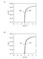
本実施例のトランジスタにおけるドレイン電流(Ids)−ゲート電圧(Vgs)測定結果について図14に示す。測定は、基板面内で25点行っており、図14には重ねて表示している。チャネル長Lは2μmであり、チャネル幅Wは50μmである。なお、トランジスタのソース電極とドレイン電極の間の電圧Vdsは3Vとした。 FIG. 14 shows measurement results of drain current (Ids) −gate voltage (Vgs) in the transistor of this example. The measurement is performed at 25 points on the substrate surface, and is displayed in an overlapping manner in FIG. The channel length L is 2 μm and the channel width W is 50 μm. Note that the voltage Vds between the source electrode and the drain electrode of the transistor was 3V.
図14より、本実施例のトランジスタは基板面内でばらつきがないことがわかる。25点の平均のしきい値電圧は0.27Vであった。 FIG. 14 shows that the transistor of this example has no variation in the substrate plane. The average threshold voltage of 25 points was 0.27V.
次に、本実施例におけるBT試験について説明する。BT試験を行うトランジスタのチャネル長Lは3μmであり、チャネル幅Wは50μmである。本実施例では、まず基板温度を25℃とし、ソース電極とドレイン電極の電圧Vdsを3Vとし、トランジスタのIds−Vgs測定を行った。 Next, the BT test in this example will be described. The transistor performing the BT test has a channel length L of 3 μm and a channel width W of 50 μm. In this example, first, the substrate temperature was set to 25 ° C., the voltage Vds between the source electrode and the drain electrode was set to 3 V, and the Ids−Vgs measurement of the transistor was performed.
次に、基板ステージ温度を150℃とし、トランジスタのソース電極を0V、ドレイン電極を0.1Vとした。次に、ゲート絶縁層に印加される電界強度が2MV/cmとなるようにゲート電極に負の電圧を印加し、そのまま1時間保持した。次に、ゲート電極の電圧を0Vとした。次に、基板温度を25℃とし、ソース電極とドレイン電極の電圧Vdsを3Vとし、トランジスタのIds−Vgs測定を行った。BT試験前後のIds−Vgs測定結果を図15(A)に示す。 Next, the substrate stage temperature was set to 150 ° C., the source electrode of the transistor was set to 0 V, and the drain electrode was set to 0.1 V. Next, a negative voltage was applied to the gate electrode so that the electric field strength applied to the gate insulating layer was 2 MV / cm, and this was maintained for 1 hour. Next, the voltage of the gate electrode was set to 0V. Next, the substrate temperature was set to 25 ° C., the voltage Vds between the source electrode and the drain electrode was set to 3 V, and Ids-Vgs measurement of the transistor was performed. The Ids-Vgs measurement results before and after the BT test are shown in FIG.
図15(A)において、細線522はBT試験前のトランジスタのIds−Vgs測定結果であり、太線524はBT試験後のトランジスタのIds−Vgs測定結果である。BT試験前から比べ、BT試験後のしきい値電圧は負方向に0.07V変動していることがわかる。 In FIG. 15A, the
同様に、測定するトランジスタを替えて、基板温度25℃とし、ソース電極とドレイン電極の電圧Vdsを3Vとし、トランジスタのIds−Vgs測定を行った。トランジスタのチャネル長Lは3μmであり、チャネル幅Wは50μmである。 Similarly, the transistor to be measured was changed, the substrate temperature was set to 25 ° C., the voltage Vds between the source electrode and the drain electrode was set to 3 V, and Ids-Vgs measurement of the transistor was performed. The transistor has a channel length L of 3 μm and a channel width W of 50 μm.
次に、基板ステージ温度を150℃とし、トランジスタのソース電極を0V、ドレイン電極を0.1Vとした。次に、ゲート絶縁層に印加される電界強度が2MV/cmとなるようにゲート電極に正の電圧を印加し、そのまま1時間保持した。次に、ゲート電極の電圧を0Vとした。次に、基板温度を25℃とし、ソース電極とドレイン電極の電圧Vdsを3Vとし、トランジスタのIds−Vgs測定を行った。BT試験前後のIds−Vgs測定結果を図15(B)に示す。 Next, the substrate stage temperature was set to 150 ° C., the source electrode of the transistor was set to 0 V, and the drain electrode was set to 0.1 V. Next, a positive voltage was applied to the gate electrode so that the electric field strength applied to the gate insulating layer was 2 MV / cm, and this was held for 1 hour. Next, the voltage of the gate electrode was set to 0V. Next, the substrate temperature was set to 25 ° C., the voltage Vds between the source electrode and the drain electrode was set to 3 V, and Ids-Vgs measurement of the transistor was performed. FIG. 15B shows the Ids-Vgs measurement results before and after the BT test.
図15(B)において、細線532はBT試験前のトランジスタのIds−Vgs測定結果であり、太線534はBT試験後のトランジスタのIds−Vgs測定結果である。BT試験前から比べ、BT試験後のしきい値電圧は正方向に0.19V変動していることがわかる。 In FIG. 15B, the
上述の通り、本実施例のトランジスタは、基板面内のしきい値電圧のばらつきが小さく、また、BT試験前後におけるしきい値電圧の変動が小さいことがわかる。 As described above, it can be seen that the transistor of this example has a small variation in threshold voltage in the substrate surface and a small variation in threshold voltage before and after the BT test.
100 基板
102 絶縁層
106 酸化物半導体層
108a ソース電極
108b ドレイン電極
112 ゲート絶縁層
114 ゲート電極
122a ソース領域
122b ドレイン領域
124 保護絶縁層
126 チャネル領域
151 トランジスタ
152 トランジスタ
153 トランジスタ
154 トランジスタ
155 トランジスタ
201 第1の基板
202 画素部
203 信号線駆動回路
204 走査線駆動回路
205 シール材
206 第2の基板
208 液晶層
210 トランジスタ
211 トランジスタ
213 液晶素子
215 接続端子電極
216 端子電極
218 FPC
218a FPC
218b FPC
219 異方性導電層
221 絶縁層
230 第1の電極層
231 第2の電極層
232 絶縁層
233 絶縁層
235 スペーサ
240 隔壁
241 電界発光層
243 発光素子
244 充填材
252 キャビティ
253 球形粒子
254 充填材
255a 黒色領域
255b 白色領域
301 本体
302 筐体
303 表示部
304 キーボード
311 本体
312 スタイラス
313 表示部
314 操作ボタン
315 外部インターフェイス
320 電子書籍
321 筐体
322 筐体
323 表示部
324 表示部
325 軸部
326 電源
327 操作キー
328 スピーカー
330 筐体
331 筐体
332 表示パネル
333 スピーカー
334 マイクロフォン
335 操作キー
336 ポインティングデバイス
337 カメラ用レンズ
338 外部接続端子
340 太陽電池セル
341 外部メモリスロット
351 本体
353 接眼部
354 操作スイッチ
355 表示部(B)
356 バッテリー
357 表示部(A)
360 テレビジョン装置
361 筐体
363 表示部
365 スタンド
500 基板
502 絶縁層
506 酸化物半導体層
508a ソース電極
508b ドレイン電極
510 トランジスタ
512 ゲート絶縁層
514 ゲート電極
516 保護絶縁層
518a ソース配線
518b ドレイン配線
522 細線
524 太線
532 細線
534 太線100
218a FPC
218b FPC
219 Anisotropic
360
Claims (5)
Translated fromJapanese前記基板上の第1の絶縁層と、
前記第1の絶縁層上の酸化物半導体層と、
前記酸化物半導体層上の第2の絶縁層と、
前記第2の絶縁層上のゲート電極と、
前記酸化物半導体層と電気的に接続するソース電極及びドレイン電極と、を有し、
前記第1の絶縁層は、前記基板側の第1の層と、前記酸化物半導体層側の第2の層とを有する積層でなり、
前記第1の層は、窒化シリコン層、窒化酸化シリコン層、酸化アルミニウム層、または窒化アルミニウム層であり、
前記第2の層は、酸化シリコン層であり、
前記第1の絶縁層は、有機層を有さず、
前記第1の絶縁層は、容量換算で、単位面積当たりの容量が2×10⁻⁴F/m2以下となる厚さを有することを特徴とする半導体装置。A substrate,
A first insulating layer on the substrate;
An oxide semiconductor layer on the first insulating layer;
A second insulating layer on the oxide semiconductor layer;
A gate electrode on the second insulating layer;
A source electrode and a drain electrode electrically connected to the oxide semiconductor layer,
The first insulating layer is a stack having a first layer on the substrate side and a second layer on the oxide semiconductor layer side,
The first layer is a silicon nitride layer, a silicon nitride oxide layer, an aluminum oxide layer, or an aluminum nitride layer;
The second layer is a silicon oxide layer;
The first insulating layer does not have an organic layer,
The first insulating layer has a thickness such that a capacitance per unit area is 2 × 10⁻⁴ F / m2 or less in terms of capacitance.
前記基板上の第1の酸化アルミニウム層と、
前記第1の酸化アルミニウム層上の、酸化シリコン又は酸化窒化シリコンを含む第1の絶縁層と、
前記第1の絶縁層上の酸化物半導体層と、
前記酸化物半導体層と電気的に接続するソース電極及びドレイン電極と、
前記酸化物半導体層上の、酸化シリコン又は酸化窒化シリコンを含む第2の絶縁層と、
前記第2の絶縁層上の第2の酸化アルミニウム層と、
前記第2の酸化アルミニウム層上のゲート電極と、を有し、
前記第1の酸化アルミニウム層と前記第1の絶縁層とでなる絶縁層は、容量換算で、単位面積当たりの容量が2×10⁻⁴F/m2以下となる厚さを有することを特徴とする半導体装置。A substrate,
A first aluminum oxide layer on the substrate;
A first insulating layer comprising silicon oxide or silicon oxynitride on the first aluminum oxide layer;
An oxide semiconductor layer on the first insulating layer;
A source electrode and a drain electrode electrically connected to the oxide semiconductor layer;
A second insulating layer containing silicon oxide or silicon oxynitride over the oxide semiconductor layer;
A second aluminum oxide layer on the second insulating layer;
A gate electrode on the second aluminum oxide layer,
The insulating layer composed of the first aluminum oxide layer and the first insulating layer has a thickness such that a capacitance per unit area is 2 × 10⁻⁴ F / m2 or less in terms of capacitance. A semiconductor device.
前記基板上の第1のゲート電極と、A first gate electrode on the substrate;
前記第1のゲート電極上の第1の絶縁層と、A first insulating layer on the first gate electrode;
前記第1の絶縁層上の酸化物半導体層と、An oxide semiconductor layer on the first insulating layer;
前記酸化物半導体層上の第2の絶縁層と、A second insulating layer on the oxide semiconductor layer;
前記第2の絶縁層上の第2のゲート電極と、A second gate electrode on the second insulating layer;
前記酸化物半導体層と電気的に接続するソース電極及びドレイン電極と、を有し、A source electrode and a drain electrode electrically connected to the oxide semiconductor layer,
前記第1の絶縁層は、前記基板側の第1の層と、前記酸化物半導体層側の第2の層とを有する積層でなり、The first insulating layer is a stack having a first layer on the substrate side and a second layer on the oxide semiconductor layer side,
前記第1の層は、窒化シリコン層、窒化酸化シリコン層、酸化アルミニウム層、または窒化アルミニウム層であり、The first layer is a silicon nitride layer, a silicon nitride oxide layer, an aluminum oxide layer, or an aluminum nitride layer;
前記第2の層は、酸化シリコン層であり、The second layer is a silicon oxide layer;
前記第1の絶縁層は、有機層を有さず、The first insulating layer does not have an organic layer,
前記第1の絶縁層は、容量換算で、単位面積当たりの容量が2×10The first insulating layer has a capacitance per unit area of 2 × 10 in terms of capacitance.−4-4F/mF / m22以下となる厚さを有することを特徴とする半導体装置。A semiconductor device having the following thickness.
前記基板上の第1のゲート電極と、A first gate electrode on the substrate;
前記第1のゲート電極上の第1の酸化アルミニウム層と、A first aluminum oxide layer on the first gate electrode;
前記第1の酸化アルミニウム層上の、酸化シリコン又は酸化窒化シリコンを含む第1の絶縁層と、A first insulating layer comprising silicon oxide or silicon oxynitride on the first aluminum oxide layer;
前記第1の絶縁層上の酸化物半導体層と、An oxide semiconductor layer on the first insulating layer;
前記酸化物半導体層と電気的に接続するソース電極及びドレイン電極と、A source electrode and a drain electrode electrically connected to the oxide semiconductor layer;
前記酸化物半導体層上の、酸化シリコン又は酸化窒化シリコンを含む第2の絶縁層と、A second insulating layer containing silicon oxide or silicon oxynitride over the oxide semiconductor layer;
前記第2の絶縁層上の第2の酸化アルミニウム層と、A second aluminum oxide layer on the second insulating layer;
前記第2の酸化アルミニウム層上の第2のゲート電極と、を有し、A second gate electrode on the second aluminum oxide layer,
前記第1の酸化アルミニウム層と前記第1の絶縁層とでなる絶縁層は、容量換算で、単位面積当たりの容量が2×10The insulating layer composed of the first aluminum oxide layer and the first insulating layer has a capacity per unit area of 2 × 10 in terms of capacity.−4-4F/mF / m22以下となる厚さを有することを特徴とする半導体装置。A semiconductor device having the following thickness.
前記酸化物半導体層は、インジウムと、亜鉛と、金属元素Mとを有し、The oxide semiconductor layer includes indium, zinc, and a metal element M,
前記金属元素Mは、Ga、Al、MnまたはCoであることを特徴とする半導体装置。The semiconductor device, wherein the metal element M is Ga, Al, Mn, or Co.
Priority Applications (1)
| Application Number | Priority Date | Filing Date | Title |
|---|---|---|---|
| JP2011110446AJP5797932B2 (en) | 2010-05-21 | 2011-05-17 | Semiconductor device |
Applications Claiming Priority (3)
| Application Number | Priority Date | Filing Date | Title |
|---|---|---|---|
| JP2010117743 | 2010-05-21 | ||
| JP2010117743 | 2010-05-21 | ||
| JP2011110446AJP5797932B2 (en) | 2010-05-21 | 2011-05-17 | Semiconductor device |
Related Child Applications (1)
| Application Number | Title | Priority Date | Filing Date |
|---|---|---|---|
| JP2015162443ADivisionJP6125581B2 (en) | 2010-05-21 | 2015-08-20 | Semiconductor device |
Publications (3)
| Publication Number | Publication Date |
|---|---|
| JP2012009835A JP2012009835A (en) | 2012-01-12 |
| JP2012009835A5 JP2012009835A5 (en) | 2014-06-19 |
| JP5797932B2true JP5797932B2 (en) | 2015-10-21 |
Family
ID=44971757
Family Applications (5)
| Application Number | Title | Priority Date | Filing Date |
|---|---|---|---|
| JP2011110446AActiveJP5797932B2 (en) | 2010-05-21 | 2011-05-17 | Semiconductor device |
| JP2015162443AActiveJP6125581B2 (en) | 2010-05-21 | 2015-08-20 | Semiconductor device |
| JP2017075180AWithdrawnJP2017135404A (en) | 2010-05-21 | 2017-04-05 | Semiconductor device |
| JP2018187337AActiveJP6595685B2 (en) | 2010-05-21 | 2018-10-02 | Transistor |
| JP2019174910AWithdrawnJP2020014010A (en) | 2010-05-21 | 2019-09-26 | Transistor |
Family Applications After (4)
| Application Number | Title | Priority Date | Filing Date |
|---|---|---|---|
| JP2015162443AActiveJP6125581B2 (en) | 2010-05-21 | 2015-08-20 | Semiconductor device |
| JP2017075180AWithdrawnJP2017135404A (en) | 2010-05-21 | 2017-04-05 | Semiconductor device |
| JP2018187337AActiveJP6595685B2 (en) | 2010-05-21 | 2018-10-02 | Transistor |
| JP2019174910AWithdrawnJP2020014010A (en) | 2010-05-21 | 2019-09-26 | Transistor |
Country Status (4)
| Country | Link |
|---|---|
| US (2) | US20110284847A1 (en) |
| JP (5) | JP5797932B2 (en) |
| TW (1) | TWI524519B (en) |
| WO (1) | WO2011145633A1 (en) |
Families Citing this family (12)
| Publication number | Priority date | Publication date | Assignee | Title |
|---|---|---|---|---|
| WO2011145634A1 (en) | 2010-05-21 | 2011-11-24 | Semiconductor Energy Laboratory Co., Ltd. | Semiconductor device |
| CN102906881B (en) | 2010-05-21 | 2016-02-10 | 株式会社半导体能源研究所 | Semiconductor device |
| KR20130077839A (en) | 2010-05-21 | 2013-07-09 | 가부시키가이샤 한도오따이 에네루기 켄큐쇼 | Semiconductor device and method of manufacturing the same |
| KR101938726B1 (en) | 2010-06-11 | 2019-01-16 | 가부시키가이샤 한도오따이 에네루기 켄큐쇼 | Semiconductor device and method for manufacturing the same |
| WO2012014952A1 (en) | 2010-07-27 | 2012-02-02 | Semiconductor Energy Laboratory Co., Ltd. | Semiconductor device and method of manufacturing the same |
| CN102651341B (en)* | 2012-01-13 | 2014-06-11 | 京东方科技集团股份有限公司 | Manufacturing method of TFT (Thin Film Transistor) array substrate |
| US8941113B2 (en)* | 2012-03-30 | 2015-01-27 | Semiconductor Energy Laboratory Co., Ltd. | Semiconductor element, semiconductor device, and manufacturing method of semiconductor element |
| US8999773B2 (en)* | 2012-04-05 | 2015-04-07 | Semiconductor Energy Laboratory Co., Ltd. | Processing method of stacked-layer film and manufacturing method of semiconductor device |
| US8901556B2 (en)* | 2012-04-06 | 2014-12-02 | Semiconductor Energy Laboratory Co., Ltd. | Insulating film, method for manufacturing semiconductor device, and semiconductor device |
| JP2014192264A (en)* | 2013-03-26 | 2014-10-06 | Nippon Hoso Kyokai <Nhk> | Thin film transistor manufacturing method |
| JPWO2019106896A1 (en)* | 2017-11-28 | 2020-11-19 | Agc株式会社 | Thin film transistor |
| JPWO2020218354A1 (en)* | 2019-04-25 | 2020-10-29 |
Family Cites Families (155)
| Publication number | Priority date | Publication date | Assignee | Title |
|---|---|---|---|---|
| JPS56116627A (en)* | 1980-02-20 | 1981-09-12 | Chiyou Lsi Gijutsu Kenkyu Kumiai | Thin film semiconductor device |
| JPS60198861A (en) | 1984-03-23 | 1985-10-08 | Fujitsu Ltd | Thin film transistor |
| JPH0244256B2 (en) | 1987-01-28 | 1990-10-03 | Kagaku Gijutsucho Mukizaishitsu Kenkyushocho | INGAZN2O5DESHIMESARERUROTSUHOSHOKEINOSOJOKOZOOJUSURUKAGOBUTSUOYOBISONOSEIZOHO |
| JPH0244260B2 (en) | 1987-02-24 | 1990-10-03 | Kagaku Gijutsucho Mukizaishitsu Kenkyushocho | INGAZN5O8DESHIMESARERUROTSUHOSHOKEINOSOJOKOZOOJUSURUKAGOBUTSUOYOBISONOSEIZOHO |
| JPH0244258B2 (en) | 1987-02-24 | 1990-10-03 | Kagaku Gijutsucho Mukizaishitsu Kenkyushocho | INGAZN3O6DESHIMESARERUROTSUHOSHOKEINOSOJOKOZOOJUSURUKAGOBUTSUOYOBISONOSEIZOHO |
| JPS63210023A (en) | 1987-02-24 | 1988-08-31 | Natl Inst For Res In Inorg Mater | Compound having a hexagonal layered structure represented by InGaZn↓4O↓7 and its manufacturing method |
| JPH0244262B2 (en) | 1987-02-27 | 1990-10-03 | Kagaku Gijutsucho Mukizaishitsu Kenkyushocho | INGAZN6O9DESHIMESARERUROTSUHOSHOKEINOSOJOKOZOOJUSURUKAGOBUTSUOYOBISONOSEIZOHO |
| JPH0244263B2 (en) | 1987-04-22 | 1990-10-03 | Kagaku Gijutsucho Mukizaishitsu Kenkyushocho | INGAZN7O10DESHIMESARERUROTSUHOSHOKEINOSOJOKOZOOJUSURUKAGOBUTSUOYOBISONOSEIZOHO |
| JPH05251705A (en) | 1992-03-04 | 1993-09-28 | Fuji Xerox Co Ltd | Thin-film transistor |
| JP3479375B2 (en) | 1995-03-27 | 2003-12-15 | 科学技術振興事業団 | Metal oxide semiconductor device in which a pn junction is formed with a thin film transistor made of a metal oxide semiconductor such as cuprous oxide, and methods for manufacturing the same |
| KR100394896B1 (en) | 1995-08-03 | 2003-11-28 | 코닌클리케 필립스 일렉트로닉스 엔.브이. | A semiconductor device including a transparent switching element |
| JP3299871B2 (en) | 1995-10-11 | 2002-07-08 | シャープ株式会社 | Liquid crystal display device and manufacturing method thereof |
| JPH09172182A (en)* | 1995-12-18 | 1997-06-30 | Semiconductor Energy Lab Co Ltd | Semiconductor device and its manufacture |
| JP3625598B2 (en) | 1995-12-30 | 2005-03-02 | 三星電子株式会社 | Manufacturing method of liquid crystal display device |
| JP3919900B2 (en)* | 1997-09-19 | 2007-05-30 | 株式会社半導体エネルギー研究所 | Liquid crystal display device and manufacturing method thereof |
| JP4170454B2 (en) | 1998-07-24 | 2008-10-22 | Hoya株式会社 | Article having transparent conductive oxide thin film and method for producing the same |
| US6656779B1 (en)* | 1998-10-06 | 2003-12-02 | Semiconductor Energy Laboratory Co., Ltd. | Semiconductor apparatus having semiconductor circuits made of semiconductor devices, and method of manufacture thereof |
| JP4450900B2 (en)* | 1998-10-06 | 2010-04-14 | 株式会社半導体エネルギー研究所 | Method for manufacturing semiconductor device |
| JP2000150861A (en) | 1998-11-16 | 2000-05-30 | Tdk Corp | Oxide thin film |
| JP3276930B2 (en) | 1998-11-17 | 2002-04-22 | 科学技術振興事業団 | Transistor and semiconductor device |
| JP2000275678A (en)* | 1999-03-26 | 2000-10-06 | Matsushita Electric Ind Co Ltd | Thin film semiconductor device and method of manufacturing the same |
| TW460731B (en) | 1999-09-03 | 2001-10-21 | Ind Tech Res Inst | Electrode structure and production method of wide viewing angle LCD |
| JP4089858B2 (en) | 2000-09-01 | 2008-05-28 | 国立大学法人東北大学 | Semiconductor device |
| KR20020038482A (en) | 2000-11-15 | 2002-05-23 | 모리시타 요이찌 | Thin film transistor array, method for producing the same, and display panel using the same |
| JP3997731B2 (en) | 2001-03-19 | 2007-10-24 | 富士ゼロックス株式会社 | Method for forming a crystalline semiconductor thin film on a substrate |
| JP2002289859A (en) | 2001-03-23 | 2002-10-04 | Minolta Co Ltd | Thin film transistor |
| JP4090716B2 (en) | 2001-09-10 | 2008-05-28 | 雅司 川崎 | Thin film transistor and matrix display device |
| JP3925839B2 (en) | 2001-09-10 | 2007-06-06 | シャープ株式会社 | Semiconductor memory device and test method thereof |
| JP4164562B2 (en) | 2002-09-11 | 2008-10-15 | 独立行政法人科学技術振興機構 | Transparent thin film field effect transistor using homologous thin film as active layer |
| WO2003040441A1 (en) | 2001-11-05 | 2003-05-15 | Japan Science And Technology Agency | Natural superlattice homologous single crystal thin film, method for preparation thereof, and device using said single crystal thin film |
| JP4083486B2 (en) | 2002-02-21 | 2008-04-30 | 独立行政法人科学技術振興機構 | Method for producing LnCuO (S, Se, Te) single crystal thin film |
| CN1445821A (en) | 2002-03-15 | 2003-10-01 | 三洋电机株式会社 | Forming method of ZnO film and ZnO semiconductor layer, semiconductor element and manufacturing method thereof |
| JP3933591B2 (en) | 2002-03-26 | 2007-06-20 | 淳二 城戸 | Organic electroluminescent device |
| US7339187B2 (en) | 2002-05-21 | 2008-03-04 | State Of Oregon Acting By And Through The Oregon State Board Of Higher Education On Behalf Of Oregon State University | Transistor structures |
| JP2004022625A (en) | 2002-06-13 | 2004-01-22 | Murata Mfg Co Ltd | Semiconductor device and method of manufacturing the semiconductor device |
| US7105868B2 (en) | 2002-06-24 | 2006-09-12 | Cermet, Inc. | High-electron mobility transistor with zinc oxide |
| US7067843B2 (en) | 2002-10-11 | 2006-06-27 | E. I. Du Pont De Nemours And Company | Transparent oxide semiconductor thin film transistors |
| JP4166105B2 (en) | 2003-03-06 | 2008-10-15 | シャープ株式会社 | Semiconductor device and manufacturing method thereof |
| JP2004273732A (en) | 2003-03-07 | 2004-09-30 | Sharp Corp | Active matrix substrate and manufacturing method thereof |
| JP4141309B2 (en)* | 2003-04-15 | 2008-08-27 | シャープ株式会社 | Semiconductor device and manufacturing method thereof |
| JP2004327649A (en)* | 2003-04-24 | 2004-11-18 | Nec Corp | Semiconductor device, thin film transistor, and method of manufacturing semiconductor device |
| JP4108633B2 (en) | 2003-06-20 | 2008-06-25 | シャープ株式会社 | THIN FILM TRANSISTOR, MANUFACTURING METHOD THEREOF, AND ELECTRONIC DEVICE |
| JP2005057238A (en)* | 2003-07-22 | 2005-03-03 | Seiko Epson Corp | Method for manufacturing electronic device, method for manufacturing semiconductor device |
| US7262463B2 (en) | 2003-07-25 | 2007-08-28 | Hewlett-Packard Development Company, L.P. | Transistor including a deposited channel region having a doped portion |
| US7145174B2 (en) | 2004-03-12 | 2006-12-05 | Hewlett-Packard Development Company, Lp. | Semiconductor device |
| US7282782B2 (en) | 2004-03-12 | 2007-10-16 | Hewlett-Packard Development Company, L.P. | Combined binary oxide semiconductor device |
| US7297977B2 (en) | 2004-03-12 | 2007-11-20 | Hewlett-Packard Development Company, L.P. | Semiconductor device |
| CN1998087B (en) | 2004-03-12 | 2014-12-31 | 独立行政法人科学技术振兴机构 | Amorphous oxide and thin film transistor |
| US7211825B2 (en) | 2004-06-14 | 2007-05-01 | Yi-Chi Shih | Indium oxide-based thin film transistors and circuits |
| JP2006100760A (en) | 2004-09-02 | 2006-04-13 | Casio Comput Co Ltd | Thin film transistor and manufacturing method thereof |
| US7285501B2 (en) | 2004-09-17 | 2007-10-23 | Hewlett-Packard Development Company, L.P. | Method of forming a solution processed device |
| US7298084B2 (en) | 2004-11-02 | 2007-11-20 | 3M Innovative Properties Company | Methods and displays utilizing integrated zinc oxide row and column drivers in conjunction with organic light emitting diodes |
| US7791072B2 (en) | 2004-11-10 | 2010-09-07 | Canon Kabushiki Kaisha | Display |
| US7453065B2 (en)* | 2004-11-10 | 2008-11-18 | Canon Kabushiki Kaisha | Sensor and image pickup device |
| KR100953596B1 (en) | 2004-11-10 | 2010-04-21 | 캐논 가부시끼가이샤 | Light emitting device |
| US7829444B2 (en) | 2004-11-10 | 2010-11-09 | Canon Kabushiki Kaisha | Field effect transistor manufacturing method |
| US7863611B2 (en) | 2004-11-10 | 2011-01-04 | Canon Kabushiki Kaisha | Integrated circuits utilizing amorphous oxides |
| EP2453481B1 (en) | 2004-11-10 | 2017-01-11 | Canon Kabushiki Kaisha | Field effect transistor with amorphous oxide |
| JP5126729B2 (en) | 2004-11-10 | 2013-01-23 | キヤノン株式会社 | Image display device |
| AU2005302964B2 (en) | 2004-11-10 | 2010-11-04 | Canon Kabushiki Kaisha | Field effect transistor employing an amorphous oxide |
| US7579224B2 (en) | 2005-01-21 | 2009-08-25 | Semiconductor Energy Laboratory Co., Ltd. | Method for manufacturing a thin film semiconductor device |
| TWI505473B (en) | 2005-01-28 | 2015-10-21 | Semiconductor Energy Lab | Semiconductor device, electronic device, and method of manufacturing semiconductor device |
| TWI445178B (en) | 2005-01-28 | 2014-07-11 | Semiconductor Energy Lab | Semiconductor device, electronic device, and method of manufacturing semiconductor device |
| US7393761B2 (en)* | 2005-01-31 | 2008-07-01 | Tokyo Electron Limited | Method for fabricating a semiconductor device |
| US7858451B2 (en) | 2005-02-03 | 2010-12-28 | Semiconductor Energy Laboratory Co., Ltd. | Electronic device, semiconductor device and manufacturing method thereof |
| US7948171B2 (en) | 2005-02-18 | 2011-05-24 | Semiconductor Energy Laboratory Co., Ltd. | Light emitting device |
| US20060197092A1 (en) | 2005-03-03 | 2006-09-07 | Randy Hoffman | System and method for forming conductive material on a substrate |
| US8681077B2 (en) | 2005-03-18 | 2014-03-25 | Semiconductor Energy Laboratory Co., Ltd. | Semiconductor device, and display device, driving method and electronic apparatus thereof |
| US7544967B2 (en) | 2005-03-28 | 2009-06-09 | Massachusetts Institute Of Technology | Low voltage flexible organic/transparent transistor for selective gas sensing, photodetecting and CMOS device applications |
| US7645478B2 (en) | 2005-03-31 | 2010-01-12 | 3M Innovative Properties Company | Methods of making displays |
| US8300031B2 (en) | 2005-04-20 | 2012-10-30 | Semiconductor Energy Laboratory Co., Ltd. | Semiconductor device comprising transistor having gate and drain connected through a current-voltage conversion element |
| JP2006324368A (en)* | 2005-05-18 | 2006-11-30 | Dainippon Printing Co Ltd | Thin film transistor mounted panel and method for manufacturing the same |
| US7651932B2 (en)* | 2005-05-31 | 2010-01-26 | Semiconductor Energy Laboratory Co., Ltd. | Method for manufacturing antenna and method for manufacturing semiconductor device |
| JP2006344849A (en) | 2005-06-10 | 2006-12-21 | Casio Comput Co Ltd | Thin film transistor |
| US7402506B2 (en) | 2005-06-16 | 2008-07-22 | Eastman Kodak Company | Methods of making thin film transistors comprising zinc-oxide-based semiconductor materials and transistors made thereby |
| US7691666B2 (en) | 2005-06-16 | 2010-04-06 | Eastman Kodak Company | Methods of making thin film transistors comprising zinc-oxide-based semiconductor materials and transistors made thereby |
| US7507618B2 (en) | 2005-06-27 | 2009-03-24 | 3M Innovative Properties Company | Method for making electronic devices using metal oxide nanoparticles |
| KR100711890B1 (en) | 2005-07-28 | 2007-04-25 | 삼성에스디아이 주식회사 | OLED display and manufacturing method thereof |
| JP2007059128A (en) | 2005-08-23 | 2007-03-08 | Canon Inc | Organic EL display device and manufacturing method thereof |
| JP4280736B2 (en) | 2005-09-06 | 2009-06-17 | キヤノン株式会社 | Semiconductor element |
| JP2007073705A (en) | 2005-09-06 | 2007-03-22 | Canon Inc | Oxide semiconductor channel thin film transistor and method for manufacturing the same |
| JP4850457B2 (en) | 2005-09-06 | 2012-01-11 | キヤノン株式会社 | Thin film transistor and thin film diode |
| JP5116225B2 (en) | 2005-09-06 | 2013-01-09 | キヤノン株式会社 | Manufacturing method of oxide semiconductor device |
| EP1770788A3 (en) | 2005-09-29 | 2011-09-21 | Semiconductor Energy Laboratory Co., Ltd. | Semiconductor device having oxide semiconductor layer and manufacturing method thereof |
| JP5037808B2 (en) | 2005-10-20 | 2012-10-03 | キヤノン株式会社 | Field effect transistor using amorphous oxide, and display device using the transistor |
| CN101577231B (en) | 2005-11-15 | 2013-01-02 | 株式会社半导体能源研究所 | Semiconductor device and method of manufacturing the same |
| TWI292281B (en) | 2005-12-29 | 2008-01-01 | Ind Tech Res Inst | Pixel structure of active organic light emitting diode and method of fabricating the same |
| US7867636B2 (en) | 2006-01-11 | 2011-01-11 | Murata Manufacturing Co., Ltd. | Transparent conductive film and method for manufacturing the same |
| JP4977478B2 (en) | 2006-01-21 | 2012-07-18 | 三星電子株式会社 | ZnO film and method of manufacturing TFT using the same |
| US7576394B2 (en) | 2006-02-02 | 2009-08-18 | Kochi Industrial Promotion Center | Thin film transistor including low resistance conductive thin films and manufacturing method thereof |
| US7977169B2 (en) | 2006-02-15 | 2011-07-12 | Kochi Industrial Promotion Center | Semiconductor device including active layer made of zinc oxide with controlled orientations and manufacturing method thereof |
| JP2007250982A (en) | 2006-03-17 | 2007-09-27 | Canon Inc | Thin film transistor and display device using oxide semiconductor |
| KR20070101595A (en) | 2006-04-11 | 2007-10-17 | 삼성전자주식회사 | ZnO TFT |
| US20070252928A1 (en) | 2006-04-28 | 2007-11-01 | Toppan Printing Co., Ltd. | Structure, transmission type liquid crystal display, reflection type display and manufacturing method thereof |
| JP5028033B2 (en) | 2006-06-13 | 2012-09-19 | キヤノン株式会社 | Oxide semiconductor film dry etching method |
| JP4999400B2 (en) | 2006-08-09 | 2012-08-15 | キヤノン株式会社 | Oxide semiconductor film dry etching method |
| JP4609797B2 (en) | 2006-08-09 | 2011-01-12 | Nec液晶テクノロジー株式会社 | Thin film device and manufacturing method thereof |
| US7651896B2 (en) | 2006-08-30 | 2010-01-26 | Semiconductor Energy Laboratory Co., Ltd. | Method for manufacturing semiconductor device |
| JP5216276B2 (en)* | 2006-08-30 | 2013-06-19 | 株式会社半導体エネルギー研究所 | Method for manufacturing semiconductor device |
| JP4332545B2 (en) | 2006-09-15 | 2009-09-16 | キヤノン株式会社 | Field effect transistor and manufacturing method thereof |
| JP4274219B2 (en) | 2006-09-27 | 2009-06-03 | セイコーエプソン株式会社 | Electronic devices, organic electroluminescence devices, organic thin film semiconductor devices |
| JP5164357B2 (en) | 2006-09-27 | 2013-03-21 | キヤノン株式会社 | Semiconductor device and manufacturing method of semiconductor device |
| US7622371B2 (en) | 2006-10-10 | 2009-11-24 | Hewlett-Packard Development Company, L.P. | Fused nanocrystal thin film semiconductor and method |
| JP2008112909A (en)* | 2006-10-31 | 2008-05-15 | Kochi Prefecture Sangyo Shinko Center | Thin film semiconductor device and manufacturing method thereof |
| US7772021B2 (en) | 2006-11-29 | 2010-08-10 | Samsung Electronics Co., Ltd. | Flat panel displays comprising a thin-film transistor having a semiconductive oxide in its channel and methods of fabricating the same for use in flat panel displays |
| JP2008140684A (en) | 2006-12-04 | 2008-06-19 | Toppan Printing Co Ltd | Color EL display and manufacturing method thereof |
| KR101303578B1 (en) | 2007-01-05 | 2013-09-09 | 삼성전자주식회사 | Etching method of thin film |
| US8207063B2 (en) | 2007-01-26 | 2012-06-26 | Eastman Kodak Company | Process for atomic layer deposition |
| KR100851215B1 (en) | 2007-03-14 | 2008-08-07 | 삼성에스디아이 주식회사 | Thin film transistor and organic light emitting display device using same |
| US7795613B2 (en) | 2007-04-17 | 2010-09-14 | Toppan Printing Co., Ltd. | Structure with transistor |
| KR101325053B1 (en) | 2007-04-18 | 2013-11-05 | 삼성디스플레이 주식회사 | Thin film transistor substrate and manufacturing method thereof |
| KR20080094300A (en) | 2007-04-19 | 2008-10-23 | 삼성전자주식회사 | Thin film transistors and methods of manufacturing the same and flat panel displays comprising thin film transistors |
| KR101334181B1 (en) | 2007-04-20 | 2013-11-28 | 삼성전자주식회사 | Thin Film Transistor having selectively crystallized channel layer and method of manufacturing the same |
| CN101663762B (en) | 2007-04-25 | 2011-09-21 | 佳能株式会社 | Oxynitride semiconductor |
| JP5043499B2 (en)* | 2007-05-02 | 2012-10-10 | 財団法人高知県産業振興センター | Electronic device and method for manufacturing electronic device |
| KR101345376B1 (en) | 2007-05-29 | 2013-12-24 | 삼성전자주식회사 | Fabrication method of ZnO family Thin film transistor |
| JP2009016469A (en)* | 2007-07-03 | 2009-01-22 | Mitsubishi Electric Corp | Semiconductor device and manufacturing method thereof |
| JP2009065012A (en) | 2007-09-07 | 2009-03-26 | Konica Minolta Holdings Inc | Thin film transistor |
| JP2009099847A (en)* | 2007-10-18 | 2009-05-07 | Canon Inc | THIN FILM TRANSISTOR, ITS MANUFACTURING METHOD, AND DISPLAY DEVICE |
| JP5268132B2 (en)* | 2007-10-30 | 2013-08-21 | 富士フイルム株式会社 | Oxide semiconductor element and manufacturing method thereof, thin film sensor, and electro-optical device |
| JP5213422B2 (en) | 2007-12-04 | 2013-06-19 | キヤノン株式会社 | Oxide semiconductor element having insulating layer and display device using the same |
| CN101897031B (en) | 2007-12-13 | 2013-04-17 | 出光兴产株式会社 | Field-effect transistor using oxide semiconductor and manufacturing method thereof |
| US8202365B2 (en) | 2007-12-17 | 2012-06-19 | Fujifilm Corporation | Process for producing oriented inorganic crystalline film, and semiconductor device using the oriented inorganic crystalline film |
| US20090278120A1 (en)* | 2008-05-09 | 2009-11-12 | Korea Institute Of Science And Technology | Thin Film Transistor |
| KR101496148B1 (en) | 2008-05-15 | 2015-02-27 | 삼성전자주식회사 | Semiconductor device and manufacturing method thereof |
| JP5403390B2 (en) | 2008-05-16 | 2014-01-29 | 出光興産株式会社 | Oxides containing indium, gallium and zinc |
| US8053253B2 (en)* | 2008-06-06 | 2011-11-08 | Semiconductor Energy Laboratory Co., Ltd. | Method for manufacturing semiconductor device |
| JP5510767B2 (en)* | 2008-06-19 | 2014-06-04 | 出光興産株式会社 | Thin film transistor and manufacturing method thereof |
| JP5430248B2 (en) | 2008-06-24 | 2014-02-26 | 富士フイルム株式会社 | Thin film field effect transistor and display device |
| KR100963026B1 (en)* | 2008-06-30 | 2010-06-10 | 삼성모바일디스플레이주식회사 | Thin film transistor, its manufacturing method, and flat panel display device comprising thin film transistor |
| JP5608347B2 (en) | 2008-08-08 | 2014-10-15 | 株式会社半導体エネルギー研究所 | Semiconductor device and manufacturing method of semiconductor device |
| JP5480554B2 (en) | 2008-08-08 | 2014-04-23 | 株式会社半導体エネルギー研究所 | Semiconductor device |
| JP5627071B2 (en) | 2008-09-01 | 2014-11-19 | 株式会社半導体エネルギー研究所 | Method for manufacturing semiconductor device |
| US9082857B2 (en) | 2008-09-01 | 2015-07-14 | Semiconductor Energy Laboratory Co., Ltd. | Semiconductor device comprising an oxide semiconductor layer |
| JP5258467B2 (en) | 2008-09-11 | 2013-08-07 | 富士フイルム株式会社 | Thin film field effect transistor and display device using the same |
| JP2010073733A (en)* | 2008-09-16 | 2010-04-02 | Fujifilm Corp | Transistor substrate and organic electroluminescent display device |
| JP4623179B2 (en) | 2008-09-18 | 2011-02-02 | ソニー株式会社 | Thin film transistor and manufacturing method thereof |
| WO2010032602A1 (en)* | 2008-09-18 | 2010-03-25 | Semiconductor Energy Laboratory Co., Ltd. | Semiconductor device |
| JP5515266B2 (en)* | 2008-09-30 | 2014-06-11 | 大日本印刷株式会社 | Thin film transistor substrate for display and manufacturing method thereof |
| JP5451280B2 (en) | 2008-10-09 | 2014-03-26 | キヤノン株式会社 | Wurtzite crystal growth substrate, manufacturing method thereof, and semiconductor device |
| JP2010093172A (en)* | 2008-10-10 | 2010-04-22 | Fujifilm Corp | Sealed device |
| US8445903B2 (en) | 2008-10-23 | 2013-05-21 | Idemitsu Kosan Co., Ltd. | Thin film transistor having a crystalline semiconductor film including indium oxide which contains a hydrogen element and method for manufacturing same |
| JP5616012B2 (en)* | 2008-10-24 | 2014-10-29 | 株式会社半導体エネルギー研究所 | Method for manufacturing semiconductor device |
| KR101578694B1 (en)* | 2009-06-02 | 2015-12-21 | 엘지디스플레이 주식회사 | Manufacturing method of oxide thin film transistor |
| KR101810699B1 (en) | 2009-06-30 | 2018-01-25 | 가부시키가이샤 한도오따이 에네루기 켄큐쇼 | Method for manufacturing semiconductor device |
| KR101791370B1 (en) | 2009-07-10 | 2017-10-27 | 가부시키가이샤 한도오따이 에네루기 켄큐쇼 | Semiconductor device |
| CN104157694A (en) | 2009-09-30 | 2014-11-19 | 大日本印刷株式会社 | Substrate for flexible device, flexible device, thin film transistor and method for manufacturing same |
| JP5732740B2 (en)* | 2009-09-30 | 2015-06-10 | 大日本印刷株式会社 | Thin film transistor substrate for flexible device and flexible device |
| JP5448960B2 (en)* | 2010-03-23 | 2014-03-19 | 富士フイルム株式会社 | Thin film transistor substrate, display device including the same, and electromagnetic wave sensor |
| JP5708910B2 (en)* | 2010-03-30 | 2015-04-30 | ソニー株式会社 | THIN FILM TRANSISTOR, MANUFACTURING METHOD THEREOF, AND DISPLAY DEVICE |
| JP2012124446A (en) | 2010-04-07 | 2012-06-28 | Kobe Steel Ltd | Oxide for semiconductor layer of thin film transistor and sputtering target, and thin film transistor |
| KR20130077839A (en) | 2010-05-21 | 2013-07-09 | 가부시키가이샤 한도오따이 에네루기 켄큐쇼 | Semiconductor device and method of manufacturing the same |
| WO2011145634A1 (en) | 2010-05-21 | 2011-11-24 | Semiconductor Energy Laboratory Co., Ltd. | Semiconductor device |
| CN102906881B (en) | 2010-05-21 | 2016-02-10 | 株式会社半导体能源研究所 | Semiconductor device |
| KR101938726B1 (en) | 2010-06-11 | 2019-01-16 | 가부시키가이샤 한도오따이 에네루기 켄큐쇼 | Semiconductor device and method for manufacturing the same |
- 2011
- 2011-05-11WOPCT/JP2011/061351patent/WO2011145633A1/enactiveApplication Filing
- 2011-05-17JPJP2011110446Apatent/JP5797932B2/enactiveActive
- 2011-05-18USUS13/110,245patent/US20110284847A1/ennot_activeAbandoned
- 2011-05-19TWTW100117579Apatent/TWI524519B/ennot_activeIP Right Cessation
- 2014
- 2014-05-19USUS14/281,031patent/US9577108B2/enactiveActive
- 2015
- 2015-08-20JPJP2015162443Apatent/JP6125581B2/enactiveActive
- 2017
- 2017-04-05JPJP2017075180Apatent/JP2017135404A/ennot_activeWithdrawn
- 2018
- 2018-10-02JPJP2018187337Apatent/JP6595685B2/enactiveActive
- 2019
- 2019-09-26JPJP2019174910Apatent/JP2020014010A/ennot_activeWithdrawn
Also Published As
| Publication number | Publication date |
|---|---|
| JP2019004185A (en) | 2019-01-10 |
| JP2020014010A (en) | 2020-01-23 |
| JP2012009835A (en) | 2012-01-12 |
| JP2016021579A (en) | 2016-02-04 |
| WO2011145633A1 (en) | 2011-11-24 |
| JP2017135404A (en) | 2017-08-03 |
| JP6595685B2 (en) | 2019-10-23 |
| US20140252347A1 (en) | 2014-09-11 |
| US20110284847A1 (en) | 2011-11-24 |
| US9577108B2 (en) | 2017-02-21 |
| TW201203553A (en) | 2012-01-16 |
| TWI524519B (en) | 2016-03-01 |
| JP6125581B2 (en) | 2017-05-10 |
Similar Documents
| Publication | Publication Date | Title |
|---|---|---|
| JP6487078B2 (en) | Method for manufacturing semiconductor device | |
| JP6721751B2 (en) | Semiconductor device | |
| JP6305581B2 (en) | Semiconductor device | |
| JP6240698B2 (en) | Semiconductor device | |
| JP5723216B2 (en) | Method for manufacturing semiconductor device | |
| JP6595685B2 (en) | Transistor | |
| JP6360224B2 (en) | Semiconductor device | |
| JP6328735B2 (en) | Semiconductor device |
Legal Events
| Date | Code | Title | Description |
|---|---|---|---|
| A521 | Request for written amendment filed | Free format text:JAPANESE INTERMEDIATE CODE: A523 Effective date:20140501 | |
| A621 | Written request for application examination | Free format text:JAPANESE INTERMEDIATE CODE: A621 Effective date:20140501 | |
| A977 | Report on retrieval | Free format text:JAPANESE INTERMEDIATE CODE: A971007 Effective date:20150309 | |
| A131 | Notification of reasons for refusal | Free format text:JAPANESE INTERMEDIATE CODE: A131 Effective date:20150317 | |
| A521 | Request for written amendment filed | Free format text:JAPANESE INTERMEDIATE CODE: A523 Effective date:20150414 | |
| TRDD | Decision of grant or rejection written | ||
| A01 | Written decision to grant a patent or to grant a registration (utility model) | Free format text:JAPANESE INTERMEDIATE CODE: A01 Effective date:20150721 | |
| A61 | First payment of annual fees (during grant procedure) | Free format text:JAPANESE INTERMEDIATE CODE: A61 Effective date:20150820 | |
| R150 | Certificate of patent or registration of utility model | Ref document number:5797932 Country of ref document:JP Free format text:JAPANESE INTERMEDIATE CODE: R150 | |
| R250 | Receipt of annual fees | Free format text:JAPANESE INTERMEDIATE CODE: R250 | |
| R250 | Receipt of annual fees | Free format text:JAPANESE INTERMEDIATE CODE: R250 | |
| R250 | Receipt of annual fees | Free format text:JAPANESE INTERMEDIATE CODE: R250 | |
| R250 | Receipt of annual fees | Free format text:JAPANESE INTERMEDIATE CODE: R250 | |
| R250 | Receipt of annual fees | Free format text:JAPANESE INTERMEDIATE CODE: R250 | |
| R250 | Receipt of annual fees | Free format text:JAPANESE INTERMEDIATE CODE: R250 | |
| R250 | Receipt of annual fees | Free format text:JAPANESE INTERMEDIATE CODE: R250 | |
| R250 | Receipt of annual fees | Free format text:JAPANESE INTERMEDIATE CODE: R250 |