JP5780981B2 - Method for forming germanium thin film - Google Patents
Method for forming germanium thin filmDownload PDFInfo
- Publication number
- JP5780981B2 JP5780981B2JP2012046829AJP2012046829AJP5780981B2JP 5780981 B2JP5780981 B2JP 5780981B2JP 2012046829 AJP2012046829 AJP 2012046829AJP 2012046829 AJP2012046829 AJP 2012046829AJP 5780981 B2JP5780981 B2JP 5780981B2
- Authority
- JP
- Japan
- Prior art keywords
- germanium
- geh
- thin film
- forming
- gas
- Prior art date
- Legal status (The legal status is an assumption and is not a legal conclusion. Google has not performed a legal analysis and makes no representation as to the accuracy of the status listed.)
- Active
Links
Images


Classifications
- H—ELECTRICITY
- H01—ELECTRIC ELEMENTS
- H01L—SEMICONDUCTOR DEVICES NOT COVERED BY CLASS H10
- H01L21/00—Processes or apparatus adapted for the manufacture or treatment of semiconductor or solid state devices or of parts thereof
- H01L21/02—Manufacture or treatment of semiconductor devices or of parts thereof
- H01L21/02104—Forming layers
- H01L21/02365—Forming inorganic semiconducting materials on a substrate
- H01L21/02436—Intermediate layers between substrates and deposited layers
- H01L21/02439—Materials
- H01L21/02441—Group 14 semiconducting materials
- H01L21/0245—Silicon, silicon germanium, germanium
- H—ELECTRICITY
- H01—ELECTRIC ELEMENTS
- H01L—SEMICONDUCTOR DEVICES NOT COVERED BY CLASS H10
- H01L21/00—Processes or apparatus adapted for the manufacture or treatment of semiconductor or solid state devices or of parts thereof
- H01L21/67—Apparatus specially adapted for handling semiconductor or electric solid state devices during manufacture or treatment thereof; Apparatus specially adapted for handling wafers during manufacture or treatment of semiconductor or electric solid state devices or components ; Apparatus not specifically provided for elsewhere
- H01L21/67005—Apparatus not specifically provided for elsewhere
- H01L21/67011—Apparatus for manufacture or treatment
- H01L21/67017—Apparatus for fluid treatment
- H—ELECTRICITY
- H01—ELECTRIC ELEMENTS
- H01L—SEMICONDUCTOR DEVICES NOT COVERED BY CLASS H10
- H01L21/00—Processes or apparatus adapted for the manufacture or treatment of semiconductor or solid state devices or of parts thereof
- H01L21/02—Manufacture or treatment of semiconductor devices or of parts thereof
- H01L21/02104—Forming layers
- H01L21/02365—Forming inorganic semiconducting materials on a substrate
- H01L21/02436—Intermediate layers between substrates and deposited layers
- H01L21/02439—Materials
- H01L21/02488—Insulating materials
- H—ELECTRICITY
- H01—ELECTRIC ELEMENTS
- H01L—SEMICONDUCTOR DEVICES NOT COVERED BY CLASS H10
- H01L21/00—Processes or apparatus adapted for the manufacture or treatment of semiconductor or solid state devices or of parts thereof
- H01L21/02—Manufacture or treatment of semiconductor devices or of parts thereof
- H01L21/02104—Forming layers
- H01L21/02365—Forming inorganic semiconducting materials on a substrate
- H01L21/02436—Intermediate layers between substrates and deposited layers
- H01L21/02494—Structure
- H01L21/02496—Layer structure
- H01L21/02502—Layer structure consisting of two layers
- H—ELECTRICITY
- H01—ELECTRIC ELEMENTS
- H01L—SEMICONDUCTOR DEVICES NOT COVERED BY CLASS H10
- H01L21/00—Processes or apparatus adapted for the manufacture or treatment of semiconductor or solid state devices or of parts thereof
- H01L21/02—Manufacture or treatment of semiconductor devices or of parts thereof
- H01L21/02104—Forming layers
- H01L21/02365—Forming inorganic semiconducting materials on a substrate
- H01L21/02518—Deposited layers
- H01L21/02521—Materials
- H01L21/02524—Group 14 semiconducting materials
- H01L21/02532—Silicon, silicon germanium, germanium
- H—ELECTRICITY
- H01—ELECTRIC ELEMENTS
- H01L—SEMICONDUCTOR DEVICES NOT COVERED BY CLASS H10
- H01L21/00—Processes or apparatus adapted for the manufacture or treatment of semiconductor or solid state devices or of parts thereof
- H01L21/02—Manufacture or treatment of semiconductor devices or of parts thereof
- H01L21/02104—Forming layers
- H01L21/02365—Forming inorganic semiconducting materials on a substrate
- H01L21/02612—Formation types
- H01L21/02617—Deposition types
- H01L21/0262—Reduction or decomposition of gaseous compounds, e.g. CVD
- H—ELECTRICITY
- H01—ELECTRIC ELEMENTS
- H01L—SEMICONDUCTOR DEVICES NOT COVERED BY CLASS H10
- H01L21/00—Processes or apparatus adapted for the manufacture or treatment of semiconductor or solid state devices or of parts thereof
- H01L21/02—Manufacture or treatment of semiconductor devices or of parts thereof
- H01L21/02104—Forming layers
- H01L21/02365—Forming inorganic semiconducting materials on a substrate
- H01L21/02612—Formation types
- H01L21/02617—Deposition types
- H01L21/02636—Selective deposition, e.g. simultaneous growth of mono- and non-monocrystalline semiconductor materials
Landscapes
- Engineering & Computer Science (AREA)
- Physics & Mathematics (AREA)
- Condensed Matter Physics & Semiconductors (AREA)
- General Physics & Mathematics (AREA)
- Manufacturing & Machinery (AREA)
- Computer Hardware Design (AREA)
- Microelectronics & Electronic Packaging (AREA)
- Power Engineering (AREA)
- Chemical Vapour Deposition (AREA)
Description
Translated fromJapaneseこの発明は、ゲルマニウム薄膜の成膜方法に関する。 The present invention relates to a method for forming a germanium thin film.
半導体材料として、IV族元素であるゲルマニウム(Ge)が知られている。ゲルマニウムは、古くから半導体デバイスに用いられていた材料ではあるが、現在ではシリコンが多く使われている。 Germanium (Ge), which is a group IV element, is known as a semiconductor material. Germanium is a material that has been used for semiconductor devices for a long time, but nowadays silicon is often used.
しかし、ゲルマニウムは、元来、シリコンよりもキャリアの移動度が高い。このため、近時、高効率太陽電池用の材料やポストシリコン世代の材料として、再び注目を集めている。 However, germanium originally has higher carrier mobility than silicon. For this reason, it has recently attracted attention as a material for high-efficiency solar cells and a material for the post-silicon generation.
ゲルマニウムを取り扱う上でネックとなるのが、絶縁膜などの下地上に、いかにして表面が滑らかなゲルマニウム薄膜を成膜するか、である。この事情に対して、特許文献1においては、表面に絶縁膜を備えた基板を第1の温度に加熱してジボラン(B2H6)又はジボラン/シラン(SiH4)混合ガスを供給し、このあと、モノゲルマン(GeH4)含有ガスを供給する。特許文献1では、絶縁膜の表面を、ホウ素ドープシリコン層によって十分に被覆してからゲルマニウム膜を成膜することで、ゲルマニウムが均一に成長することを見出している。The bottleneck in handling germanium is how to form a germanium thin film with a smooth surface on the surface of an insulating film or the like. In this situation, in
また、特許文献2においては、二酸化シリコン(SiO2)基板上にシリコンシード層を堆積後、引き続きCVD法によってゲルマニウム膜を堆積することによって、CVD法を用いつつ、連続的で滑らかな平坦性が良好なゲルマニウム膜が得られることを見出している。In
しかしながら、特許文献1、2においては、二酸化シリコン等の下地とゲルマニウム膜との間に、ホウ素ドープシリコン層、又はシリコンシード層が介在することになる。 However, in
このように、下地とゲルマニウム膜との間に、ゲルマニウム膜とは異なる膜が介在されてしまうと、下地との密着性の低下や界面準位の発生など、半導体デバイスの特性上、懸念される構造が生じる、という事情がある。 As described above, if a film different from the germanium film is interposed between the base and the germanium film, there is a concern in terms of characteristics of the semiconductor device such as a decrease in adhesion to the base and generation of an interface state. There is a situation that a structure arises.
また、特許文献1、2においては、表面の滑らかさの改善については考慮があるものの、ゲルマニウム薄膜を、表面が滑らかで良好な平坦性、及びその膜厚の良好な均一性を維持したまま、さらに、その膜厚を薄くする、という、次の技術的段階をブレークスルーしようとすることついては、考慮されていない。 Further, in
この発明は、半導体デバイスの特性上、懸念される構造が生じることを抑えつつ、表面の良好な平坦性、及び膜厚の良好な均一性を維持したまま、その膜厚をさらに薄くすることが可能なゲルマニウム薄膜の成膜方法を提供する。 The present invention makes it possible to further reduce the film thickness while maintaining good flatness of the surface and good uniformity of the film thickness while suppressing the occurrence of a structure of concern due to the characteristics of the semiconductor device. A method for forming a germanium thin film is provided.
この発明の一態様に係るゲルマニウム薄膜の成膜方法は、下地上に、ゲルマニウム薄膜を形成するゲルマニウム薄膜の成膜方法であって、(1)アミノゲルマン系ガスを用いて、水分がある前記下地の表面にゲルマニウムを吸着させ、ゲルマニウムシード層を形成する工程と、(2)前記アミノゲルマン系ガスとは異なるゲルマン系ガスを用いて、前記ゲルマニウムシード層上にゲルマニウム薄膜を形成する工程とを具備し、前記ゲルマン系ガスが、GeH4、Ge2H6、GeCl4、GeHCl3、GeH2Cl2、GeH3Clの少なくとも一つを含むガスから選ばれる。A method for forming a germanium thin film according to an aspect of the present invention is a method for forming a germanium thin film on a base, wherein the germanium thin film is formed by using (1) an aminogermanic gas and the base havingwater And (2) forming a germanium thin film on the germanium seed layer using a germanium-based gasdifferent from the aminogerman-based gas.The germane gas isselected from a gas containing at least one ofGeH4, Ge2H6, GeCl4, GeHCl3, GeH2Cl2, and GeH3Cl .
この発明によれば、半導体デバイスの特性上、懸念される構造が生じることを抑えつつ、表面の良好な平坦性、及び膜厚の良好な均一性を維持したまま、その膜厚をさらに薄くすることが可能なゲルマニウム薄膜の成膜方法を提供できる。 According to the present invention, the thickness of the semiconductor device is further reduced while maintaining the good flatness of the surface and the good uniformity of the film thickness while suppressing the occurrence of a structure that is concerned about the characteristics of the semiconductor device. It is possible to provide a method for forming a germanium thin film.
以下、この発明の一実施形態を、図面を参照して説明する。なお、全図にわたり、共通の部分には共通の参照符号を付す。 Hereinafter, an embodiment of the present invention will be described with reference to the drawings. Note that common parts are denoted by common reference numerals throughout the drawings.
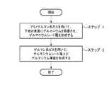
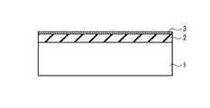
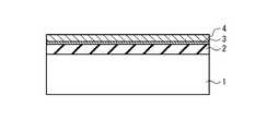
図1はこの発明の一実施形態に係るゲルマニウム薄膜の成膜方法の一例を示す流れ図、図2A〜図2Cはその成膜方法の主要な工程を示す断面図、図3A〜図3Gは膜の状態を模式的に示す図である。 FIG. 1 is a flowchart showing an example of a method for forming a germanium thin film according to an embodiment of the present invention, FIGS. 2A to 2C are cross-sectional views showing main steps of the film forming method, and FIGS. It is a figure which shows a state typically.
本例は、下地上にゲルマニウム薄膜を形成する成膜方法である。本例においては、下地の一例とし、シリコン基板(シリコンウエハ=シリコン単結晶)1上に形成されたシリコン酸化物(SiO2)膜2を用いる(図2A参照)。下地は、シリコン酸化物膜2に限られるものではないが、好ましくは、表面に水分がある膜が望ましい。水分の一例は、図3Aに示すようにヒドロキシ基(OH)である。表面にヒドロキシ基があるシリコン酸化物膜2を形成するには、例えば、シリコンの原料となるガスとして、シラン系ガスのような水素を含むガスを用いて化学的気相成長させることや、水素、例えば、水蒸気を含む雰囲気中でシリコンを酸化することなどをあげることができる。This example is a film forming method in which a germanium thin film is formed on a base. In this example, a silicon oxide (SiO2 )
次に、図1のステップ1および図2Bに示すように、アミノゲルマン系ガスを用いて、シリコン酸化物膜2の表面にゲルマニウムを吸着させ、ゲルマニウムシード層3を形成する。本例においては、アミノゲルマン系ガスとして、GeH(NMe2)3ガスを用いた。Next, as shown in
ゲルマニウムシード層3を形成する際の処理条件の一例は、
GeH(NMe2)3流量: 500sccm
処 理 時 間: 1min
処 理 温 度: 300℃
処 理 圧 力: 133Pa( 1Torr)
である。An example of the processing conditions when forming the
GeH (NMe2 )3 flow rate: 500 sccm
Processing time: 1 min
Processing temperature: 300 ℃
Processing pressure: 133 Pa (1 Torr)
It is.
シリコン酸化物膜2の表面には、水分、例えば、ヒドロキシ基が含まれている。このようなシリコン酸化物膜2の表面に、上記処理条件でアミノゲルマン系ガスを供給すると、シリコン酸化物膜2の表面のヒドロキシ基からは“水素(H)”が分離する。また、アミノゲルマン系ガスのゲルマニウム(Ge)からは“窒素(N)”とともに“炭化水素基(CxHy)”が分離する。分離した水素、窒素および炭化水素基は化合し、“アミン(CxHyN)”となって揮発していく。そして、シリコン酸化物膜2の表面の“酸素(O)”の未結合手と、窒素および炭化水素基が分離したガスの“ゲルマニウム(Ge)”の未結合手とが結合していく。このようにしてシリコン酸化物膜2の表面には、ゲルマニウムを含むゲルマニウムシード層3が形成される(図3B〜図3C参照)。The surface of the
ゲルマニウムシード層3は、シリコン酸化物膜2の表面にゲルマニウムが吸着される程度に形成されればよく、例えば、単原子層〜数原子層の厚さがあればよい(図3B〜図3C参照)。具体的な数値をあげるとするならば、0.1〜3nmであろう。 The
なお、図3B〜図3Cにおいては、図示を簡潔にするため、アミノゲルマン系ガスとして、例えば、GeH3(NMe2)のような構造を持つアミノゲルマン系ガスを示している。In FIGS. 3B to 3C, for the sake of simplicity, aminogermanic gas having a structure such as GeH3 (NMe2 ) is shown as the aminogermanic gas.
次に、図1のステップ2および図2Cに示すように、ゲルマン系ガスを用いて、ゲルマニウムシード層3上にゲルマニウム薄膜4を形成する。本例においては、ゲルマン系ガスとして、GeH4ガスを用いた。Next, as shown in
ゲルマニウム薄膜4を形成する際の処理条件の一例は、
GeH4流量 : 10〜2000sccm
処 理 時 間: 60min
処 理 温 度: 200〜500℃
処 理 圧 力: 13.3〜1333.2Pa(0.1〜10Torr)
である。An example of the processing conditions for forming the germanium
GeH4 flow rate: 10 to 2000 sccm
Processing time: 60min
Processing temperature: 200-500 ° C
Processing pressure: 13.3 to 1333.2 Pa (0.1 to 10 Torr)
It is.
上記処理条件でゲルマン系ガスをゲルマニウムシード層3の表面に供給すると、ゲルマニウムシード層3からは“水素(H)”が分離し、ゲルマン系ガスのゲルマニウム(Ge)からは“水素(H)”が分離する。分離した水素は化合し、“水素ガス(H2)”となって揮発していく。そして、ゲルマニウムシード層3の“ゲルマニウム(Ge)”の未結合手と、水素が分離したガスの“ゲルマニウム(Ge)”の未結合手とが結合していく。このようにしてゲルマニウムシード層3上に、ゲルマニウムを含むゲルマニウム薄膜4が形成されていく(図3D〜図3E参照)。また、上記反応は、ゲルマニウム薄膜4を形成している間おこり、この結果、ゲルマニウム薄膜4の膜厚は、要求された値に向かって増していく(図3F〜図3G参照)。When germanium-based gas is supplied to the surface of the
ゲルマニウム薄膜4の膜厚は、要求に応じて様々な値に設定することができる。しかも、後述するように、上記一実施形態によって形成されるゲルマニウム薄膜4は、薄い膜厚でも表面の平坦性、および膜厚の均一性が良好となる、という利点が得られる。この観点から、例えば、ゲルマニウム薄膜4は、単原子層〜数原子層レベルの薄い膜厚であってもよい。現状、又は今後、要求され得る膜厚の値をあげるとするならば、1〜50nmと予想され、この範囲であれば、実用的で好ましい膜厚であろう。 The film thickness of the germanium
図4は、ゲルマニウム薄膜の膜厚と堆積時間との関係を示す図である。 FIG. 4 is a diagram showing the relationship between the film thickness of the germanium thin film and the deposition time.
図4中の線Iは上記一実施形態に従って形成されたゲルマニウム薄膜4を示し、線IIはゲルマニウムシード層を形成せずにシリコン酸化物膜上に直接ゲルマニウム薄膜を形成した比較例を示している。 A line I in FIG. 4 shows the germanium
図4に示すように、一実施形態に従って形成されたゲルマニウム薄膜4(線I)の方が、比較例に係るゲルマニウム薄膜(線II)に比較して、堆積が始まる時間が早いことが分かる。つまり、一実施形態に従って形成されたゲルマニウム薄膜4は、インキュベーション時間が短い。インキュベーション時間が短いということは、一実施形態は、比較例に比較して、ゲルマニウム薄膜4の成長の種となる“核”が、ゲルマニウムシード層3上に稠密、かつ、均一に形成されている、ということである。一実施形態においては“核”が島状に点在しているのではなく、層状、又は極めて層状に近い形で形成されているものと考えても支障はない。 As shown in FIG. 4, it can be seen that the germanium thin film 4 (line I) formed according to the embodiment has a faster time to start deposition than the germanium thin film (line II) according to the comparative example. That is, the germanium
このように、上記一実施形態によれば、“核”が層状、又は極めて層状に近い形で形成されることによって、ゲルマニウム薄膜4の平坦性は、例えば、単原子層〜数原子層レベルの薄い膜厚の時点から、良好なものとすることができる。しかも、膜厚の均一性についても、単原子層〜数原子層レベルの薄い膜厚の時点から、良好となる。 As described above, according to the embodiment, the flatness of the germanium
さらに、上記一実施形態は、シリコン酸化物膜2上にシード層を形成するものであるが、このシード層はゲルマニウムシード層3であり、ゲルマニウム薄膜4と同種のものである。このため、ゲルマニウム膜を、シリコンなどゲルマニウム以外の物質からなるシード層上に形成していた従来に比較して、半導体デバイスの特性上、懸念される構造が生じることを抑えることができる、という利点についても得ることができる。 Further, in the above embodiment, a seed layer is formed on the
よって、一実施形態によれば、半導体デバイスの特性上、懸念される構造が生じることを抑えつつ、表面の良好な平坦性、及び膜厚の良好な均一性を維持したまま、その膜厚をさらに薄くすることが可能なゲルマニウム薄膜の成膜方法を得ることができる。 Therefore, according to one embodiment, the thickness of the semiconductor device is reduced while maintaining good flatness of the surface and good uniformity of the film thickness while suppressing the occurrence of a structure of concern on the characteristics of the semiconductor device. A film forming method of a germanium thin film that can be further thinned can be obtained.
以上、この発明を一実施形態に従って説明したが、この発明は、上記一実施形態に限定されることは無く、その趣旨を逸脱しない範囲で種々変形可能である。また、この発明の実施形態は、上記一実施形態が唯一のものでもない。 As mentioned above, although this invention was demonstrated according to one Embodiment, this invention is not limited to the said one Embodiment, A various deformation | transformation is possible in the range which does not deviate from the meaning. Further, the embodiment of the present invention is not the only one described above.
例えば、上記実施形態においては、処理条件を具体的に例示したが、処理条件は、上記具体的な例示に限られるものではない。 For example, in the above embodiment, the processing conditions are specifically exemplified, but the processing conditions are not limited to the above specific examples.
また、下地として、シリコン酸化物膜2を例示したが、下地は、シリコン酸化物膜2に限られるものではない。例えば、シリコン窒化膜であっても良いし、多結晶シリコン膜であっても、シリコン基板であってもよい。もちろん、タングステン、銅、チタン、チタンナイトライドなどの内部配線層を構成するような金属膜であってもよい。さらには、キャパシタなどの誘電体膜として使用されるようなタンタル酸化膜などシリコン酸化膜よりも高い比誘電率を持つ誘電体膜であってもよい。ただし、下地の表面には、少なくとも水分、例えば、ヒドロキシ基があることが好ましい。 Further, although the
下地の表面に水分を持たせるためには、例えば、図5に示すように、ゲルマニウムシード層3を形成する工程の前に、下地の表面に水分を与える工程(ステップ3)を、さらに具備するようにしてもよい。 In order to give moisture to the surface of the underlayer, for example, as shown in FIG. 5, a step (step 3) of providing moisture to the undersurface is further included before the step of forming the
下地の表面に水分を与える工程の例としては、
(1)下地を、水分を含む気体中にさらす工程
(2)下地を、水洗する工程
などを挙げることができる。As an example of the process of giving moisture to the surface of the foundation,
(1) The process of exposing the substrate to a gas containing moisture
(2) The process of washing the substrate with water
And so on.
また、上記(1)においては、水分を含む気体として大気を利用することも可能である。この場合、下地の表面に水分を与える工程とし、例えば、下地としてシリコン酸化物膜2が形成されたシリコン基板1を、大気中に放置するだけでもよい。 Moreover, in said (1), it is also possible to utilize air | atmosphere as a gas containing a water | moisture content. In this case, the step of supplying moisture to the surface of the base may be performed. For example, the
また、上記一実施形態においては、アミノゲルマン系ガスとして、GeH(NMe2)3を用いたが、GeH(NMe2)3の他にも、次のようなアミノゲルマン系ガスを用いることができる。In the above embodiment, GeH (NMe2 )3 is used as the aminogermanic gas. However, in addition to GeH (NMe2 )3 , the following aminogermanic gas can be used. .
GeH(NMeEt)3
GeH(NEt2)3
GeH(NHEt)3
GeH(NHi-Pr)3
GeH(NHt-Bu)3
GeH2(NMe2)2
GeH2(NMeEt)2
GeH2(NEt2)2
GeH2(NHEt)2
GeH2(NHi-Pr)2
GeH2(NHt-Bu)2
GeH3(NMe2)
GeH3(NMeEt)
GeH3(NEt2)
GeH3(NHEt)
GeH3(NHi-Pr)
GeH3(NHt-Bu)
ゲルマニウムシード層3の形成に際しては、GeH(NMe2)3および上記ガス群の中から少なくとも一つを含むガスが用いられればよい。GeH (NMeEt)3
GeH (NEt2 )3
GeH (NHEt)3
GeH (NHi-Pr)3
GeH (NHt-Bu)3
GeH2 (NMe2 )2
GeH2 (NMeEt)2
GeH2 (NEt2 )2
GeH2 (NHEt)2
GeH2 (NHi—Pr)2
GeH2 (NHt—Bu)2
GeH3 (NMe2 )
GeH3 (NMeEt)
GeH3 (NEt2 )
GeH3 (NHEt)
GeH3 (NHi-Pr)
GeH3 (NHt-Bu)
In forming the
また、ゲルマニウムシード層3の形成に際しては、ジゲルマン(Ge2H6)を用いても良い。Further, in the formation of the
なお、上記ガス群において、Meはメチル基、Etはエチル基、i-Prはイソプロピル基、t-Buはターシャリーブチル基を表している。 In the above gas group, Me represents a methyl group, Et represents an ethyl group, i-Pr represents an isopropyl group, and t-Bu represents a tertiary butyl group.
また、上記一実施形態においては、ゲルマン系ガスとして、GeH4を用いたが、GeH4の他にも、次のようなゲルマン系ガスを用いることができる。In the above-described embodiment, GeH4 is used as the germane gas, but the following germane gas can be used in addition to GeH4 .
Ge2H6
GeCl4
GeHCl3
GeH2Cl2
GeH3Cl
ゲルマニウム薄膜4の形成に際しては、GeH4および上記ガス群の中から少なくとも一つを含むガスが用いられればよい。Ge2 H6
GeCl4
GeHCl3
GeH2 Cl2
GeH3 Cl
In forming the germanium
また、ゲルマニウム薄膜4には、ドーパントがドープされていてもよい。ドーパントの例としては、
ボロン(B)
リン(P)
ヒ素(As)
酸素(O)
炭素(C)
窒素(N)
を挙げることができる。ゲルマニウム薄膜4にドーパントをドープするタイミングとしては、上記ドーパント群の少なくとも1つを、ゲルマニウム薄膜4の成膜雰囲気中に混合する、あるいは上記ドーパント群の少なくとも1つを、ゲルマニウム薄膜4の成膜後にドープする、のいずれであってもよい。
その他、この発明はその要旨を逸脱しない範囲で様々に変形することができる。The germanium
Boron (B)
Phosphorus (P)
Arsenic (As)
Oxygen (O)
Carbon (C)
Nitrogen (N)
Can be mentioned. The timing for doping the germanium
In addition, the present invention can be variously modified without departing from the gist thereof.
1…シリコン基板、2…シリコン酸化物膜、3…ゲルマニウムシード層、4…ゲルマニウム薄膜 DESCRIPTION OF
Claims (10)
Translated fromJapanese(1) アミノゲルマン系ガスを用いて、水分がある前記下地の表面にゲルマニウムを吸着させ、ゲルマニウムシード層を形成する工程と、
(2)前記アミノゲルマン系ガスとは異なるゲルマン系ガスを用いて、前記ゲルマニウムシード層上にゲルマニウム薄膜を形成する工程と
を具備し、
前記ゲルマン系ガスが、
GeH4
Ge2H6
GeCl4
GeHCl3
GeH2Cl2
GeH3Cl
の少なくとも一つを含むガスから選ばれることを特徴とするゲルマニウム薄膜の成膜方法。A germanium thin film forming method for forming a germanium thin film on the ground,
(1) using an aminogermanic gas, adsorbing germanium on the surface of the foundation havingwater , and forming a germanium seed layer;
(2) forming a germanium thin film on the germanium seed layer using a germane gasdifferent from the aminogermane gas; and
The germane gas is
GeH4
Ge2H6
GeCl4
GeHCl3
GeH2Cl2
GeH3Cl
A method for forming a germanium thin film, wherein the film isselected from gases containing at least one of the following .
(3) 前記下地の表面に水分を与える工程を、さらに具備することを特徴とする請求項1に記載のゲルマニウム薄膜の成膜方法。Before the step (1),
(3) a step of providing moisture to the surface of the underlying further method of forming a germanium thin film accordingto claim1, characterized in that it comprises.
GeH(NMe2)3
GeH(NMeEt)3
GeH(NEt2)3
GeH(NHEt)3
GeH(NHi-Pr)3
GeH(NHt-Bu)3
GeH2(NMe2)2
GeH2(NMeEt)2
GeH2(NEt2)2
GeH2(NHEt)2
GeH2(NHi-Pr)2
GeH2(NHt-Bu)2
GeH3(NMe2)
GeH3(NMeEt)
GeH3(NEt2)
GeH3(NHEt)
GeH3(NHi-Pr)
GeH3(NHt-Bu)
の少なくとも一つを含むガスから選ばれることを特徴とする請求項1から請求項6のいずれか一項に記載のゲルマニウム薄膜の成膜方法。The aminogermanic gas is
GeH (NMe2 )3
GeH (NMeEt)3
GeH (NEt2 )3
GeH (NHEt)3
GeH (NHi-Pr)3
GeH (NHt-Bu)3
GeH2 (NMe2 )2
GeH2 (NMeEt)2
GeH2 (NEt2 )2
GeH2 (NHEt)2
GeH2 (NHi—Pr)2
GeH2 (NHt—Bu)2
GeH3 (NMe2 )
GeH3 (NMeEt)
GeH3 (NEt2 )
GeH3 (NHEt)
GeH3 (NHi-Pr)
GeH3 (NHt-Bu)
The method for forming a germanium thin film according to any one ofclaims 1 to 6 , wherein the film is selected from a gas containing at least one of the following.
B
P
As
O
C
N
の少なくとも一つを含むドーパントがドープされることを特徴とする請求項1から請求項7のいずれか一項に記載のゲルマニウム薄膜の成膜方法。In the germanium thin film,
B
P
As
O
C
N
The method for forming a germanium thin film according to any one ofclaims 1 to 7 , wherein a dopant containing at least one of the above is doped.
前記水分がある前記下地の表面から水素を分離し、Separating hydrogen from the underlying surface with the moisture,
前記アミノゲルマン系ガスのゲルマニウムから窒素および炭化水素基を分離し、Separating nitrogen and hydrocarbon groups from germanium of the aminogermanic gas,
前記分離した前記水素、前記窒素および前記炭化水素基をアミンとして揮発させ、Volatilizing the separated hydrogen, nitrogen and hydrocarbon groups as amines;
前記下地の表面の酸素の未結合手に、前記窒素および炭化水素基が分離した前記ゲルマニウムの未結合手を結合させるThe germanium dangling bonds separated from the nitrogen and hydrocarbon groups are bonded to the oxygen dangling bonds on the surface of the base.
ことでなされることを特徴とする請求項1から請求項8のいずれか一項に記載のゲルマニウム薄膜の成膜方法。The method for forming a germanium thin film according to any one of claims 1 to 8, wherein the method is performed.
前記ゲルマニウムシード層から水素を分離し、Separating hydrogen from the germanium seed layer;
前記アミノゲルマン系ガスとは異なるゲルマン系ガスのゲルマニウムに結合している結合元素を分離し、Separating the binding element bonded to germanium gas germanium different from the aminogerman gas,
前記分離した前記水素および前記結合元素をガスとして揮発させ、Volatilizing the separated hydrogen and the binding element as gas,
前記ゲルマニウムシード層のゲルマニウムの未結合手に、前記結合元素が分離した前記ゲルマニウムの未結合手を結合させるThe germanium dangling bonds separated from the bonding elements are bonded to the germanium dangling bonds of the germanium seed layer.
ことを経てなされることを特徴とする請求項9に記載のゲルマニウム薄膜の成膜方法。The method of forming a germanium thin film according to claim 9, wherein
Priority Applications (5)
| Application Number | Priority Date | Filing Date | Title |
|---|---|---|---|
| JP2012046829AJP5780981B2 (en) | 2012-03-02 | 2012-03-02 | Method for forming germanium thin film |
| KR1020130022229AKR101587319B1 (en) | 2012-03-02 | 2013-02-28 | Method of forming a germanium thin film |
| US13/780,842US8815714B2 (en) | 2012-03-02 | 2013-02-28 | Method of forming a germanium thin film |
| TW102107327ATWI551716B (en) | 2012-03-02 | 2013-03-01 | Method of forming a germanium thin film |
| US14/337,603US20140331928A1 (en) | 2012-03-02 | 2014-07-22 | Method of forming a germanium thin film |
Applications Claiming Priority (1)
| Application Number | Priority Date | Filing Date | Title |
|---|---|---|---|
| JP2012046829AJP5780981B2 (en) | 2012-03-02 | 2012-03-02 | Method for forming germanium thin film |
Publications (2)
| Publication Number | Publication Date |
|---|---|
| JP2013181231A JP2013181231A (en) | 2013-09-12 |
| JP5780981B2true JP5780981B2 (en) | 2015-09-16 |
Family
ID=49043080
Family Applications (1)
| Application Number | Title | Priority Date | Filing Date |
|---|---|---|---|
| JP2012046829AActiveJP5780981B2 (en) | 2012-03-02 | 2012-03-02 | Method for forming germanium thin film |
Country Status (4)
| Country | Link |
|---|---|
| US (2) | US8815714B2 (en) |
| JP (1) | JP5780981B2 (en) |
| KR (1) | KR101587319B1 (en) |
| TW (1) | TWI551716B (en) |
Cited By (1)
| Publication number | Priority date | Publication date | Assignee | Title |
|---|---|---|---|---|
| KR101780199B1 (en) | 2013-12-06 | 2017-09-21 | 젤리스트 테크놀로지스, 인코퍼레이티드 | Method for Producing High Purity Germane by a Continuous or Semi-Continuous Process |
Families Citing this family (8)
| Publication number | Priority date | Publication date | Assignee | Title |
|---|---|---|---|---|
| US9214630B2 (en) | 2013-04-11 | 2015-12-15 | Air Products And Chemicals, Inc. | Method of making a multicomponent film |
| RU2016135995A (en)* | 2014-03-04 | 2018-04-04 | Пикосан Ой | ATOMIC-LAYER DEPOSITION OF GERMANY OR GERMANY OXIDE |
| JP6258813B2 (en)* | 2014-08-12 | 2018-01-10 | 東京エレクトロン株式会社 | Method and apparatus for forming germanium film |
| KR101635970B1 (en)* | 2015-02-17 | 2016-07-04 | 국방과학연구소 | Method for High-Quality Germanium Films Grown by Low Pressure-Chemical Vapor Deposition |
| JP6584348B2 (en)* | 2016-03-07 | 2019-10-02 | 東京エレクトロン株式会社 | Method of filling recess and processing apparatus |
| JP6585551B2 (en)* | 2016-06-15 | 2019-10-02 | 株式会社Kokusai Electric | Semiconductor device manufacturing method, substrate processing apparatus, and program |
| ES2874228T3 (en)* | 2018-11-14 | 2021-11-04 | Evonik Operations Gmbh | Tetrakis (trichlorosilyl) Germanic, process for its production |
| EP4176100A4 (en)* | 2020-07-24 | 2024-08-14 | Versum Materials US, LLC | COMPOSITIONS AND METHODS THEREOF FOR GERMANIUM SEED LAYER |
Family Cites Families (27)
| Publication number | Priority date | Publication date | Assignee | Title |
|---|---|---|---|---|
| WO1984000178A1 (en)* | 1982-06-22 | 1984-01-19 | Hughes Aircraft Co | Low temperature process for depositing epitaxial layers |
| JPH0666262B2 (en) | 1985-03-06 | 1994-08-24 | 日本電信電話株式会社 | Method for manufacturing semiconductor device |
| US5358895A (en)* | 1993-05-27 | 1994-10-25 | Motorola, Inc. | Low temperature silicon epitaxy with germanium doping |
| JP3437832B2 (en)* | 2000-03-22 | 2003-08-18 | 東京エレクトロン株式会社 | Film forming method and film forming apparatus |
| US7026219B2 (en)* | 2001-02-12 | 2006-04-11 | Asm America, Inc. | Integration of high k gate dielectric |
| JP3660897B2 (en)* | 2001-09-03 | 2005-06-15 | 株式会社ルネサステクノロジ | Manufacturing method of semiconductor device |
| US7238595B2 (en)* | 2003-03-13 | 2007-07-03 | Asm America, Inc. | Epitaxial semiconductor deposition methods and structures |
| JP4954448B2 (en)* | 2003-04-05 | 2012-06-13 | ローム・アンド・ハース・エレクトロニック・マテリアルズ,エル.エル.シー. | Organometallic compounds |
| US7166528B2 (en)* | 2003-10-10 | 2007-01-23 | Applied Materials, Inc. | Methods of selective deposition of heavily doped epitaxial SiGe |
| JP4982355B2 (en)* | 2004-02-27 | 2012-07-25 | エーエスエム アメリカ インコーポレイテッド | Method for forming germanium film |
| US7152804B1 (en)* | 2004-03-15 | 2006-12-26 | Kovlo, Inc. | MOS electronic article surveillance, RF and/or RF identification tag/device, and methods for making and using the same |
| US7312165B2 (en)* | 2004-05-05 | 2007-12-25 | Jursich Gregory M | Codeposition of hafnium-germanium oxides on substrates used in or for semiconductor devices |
| US7286053B1 (en)* | 2004-07-31 | 2007-10-23 | Kovio, Inc. | Electronic article surveillance (EAS) tag/device with coplanar and/or multiple coil circuits, an EAS tag/device with two or more memory bits, and methods for tuning the resonant frequency of an RLC EAS tag/device |
| US7648927B2 (en)* | 2005-06-21 | 2010-01-19 | Applied Materials, Inc. | Method for forming silicon-containing materials during a photoexcitation deposition process |
| US7651955B2 (en)* | 2005-06-21 | 2010-01-26 | Applied Materials, Inc. | Method for forming silicon-containing materials during a photoexcitation deposition process |
| US7678420B2 (en) | 2005-06-22 | 2010-03-16 | Sandisk 3D Llc | Method of depositing germanium films |
| KR100763916B1 (en)* | 2006-06-21 | 2007-10-05 | 삼성전자주식회사 | Fabrication Method of Thin Film Thin Film and Phase Change Memory Device Using the Same |
| KR100757415B1 (en)* | 2006-07-13 | 2007-09-10 | 삼성전자주식회사 | Germanium compound and manufacturing method thereof, phase change memory device using the germanium compound and forming method thereof |
| JP5490393B2 (en)* | 2007-10-10 | 2014-05-14 | 株式会社半導体エネルギー研究所 | Manufacturing method of semiconductor substrate |
| US7960205B2 (en)* | 2007-11-27 | 2011-06-14 | Air Products And Chemicals, Inc. | Tellurium precursors for GST films in an ALD or CVD process |
| US20090162973A1 (en)* | 2007-12-21 | 2009-06-25 | Julien Gatineau | Germanium precursors for gst film deposition |
| US8318252B2 (en)* | 2008-01-28 | 2012-11-27 | Air Products And Chemicals, Inc. | Antimony precursors for GST films in ALD/CVD processes |
| WO2009095898A1 (en)* | 2008-02-01 | 2009-08-06 | L'air Liquide-Societe Anonyme Pour L'etude Et L'exploitation Des Procedes Georges Claude | New metal precursors containing beta-diketiminato ligands |
| US7968434B2 (en) | 2008-11-14 | 2011-06-28 | Nec Corporation | Method of forming of a semiconductor film, method of manufacture of a semiconductor device and a semiconductor device |
| JP4967066B2 (en)* | 2010-04-27 | 2012-07-04 | 東京エレクトロン株式会社 | Method and apparatus for forming amorphous silicon film |
| US20120220116A1 (en)* | 2011-02-25 | 2012-08-30 | Applied Materials, Inc. | Dry Chemical Cleaning For Semiconductor Processing |
| US9171715B2 (en)* | 2012-09-05 | 2015-10-27 | Asm Ip Holding B.V. | Atomic layer deposition of GeO2 |
- 2012
- 2012-03-02JPJP2012046829Apatent/JP5780981B2/enactiveActive
- 2013
- 2013-02-28KRKR1020130022229Apatent/KR101587319B1/enactiveActive
- 2013-02-28USUS13/780,842patent/US8815714B2/enactiveActive
- 2013-03-01TWTW102107327Apatent/TWI551716B/enactive
- 2014
- 2014-07-22USUS14/337,603patent/US20140331928A1/ennot_activeAbandoned
Cited By (1)
| Publication number | Priority date | Publication date | Assignee | Title |
|---|---|---|---|---|
| KR101780199B1 (en) | 2013-12-06 | 2017-09-21 | 젤리스트 테크놀로지스, 인코퍼레이티드 | Method for Producing High Purity Germane by a Continuous or Semi-Continuous Process |
Also Published As
| Publication number | Publication date |
|---|---|
| KR101587319B1 (en) | 2016-01-20 |
| TW201346060A (en) | 2013-11-16 |
| US8815714B2 (en) | 2014-08-26 |
| TWI551716B (en) | 2016-10-01 |
| US20130230975A1 (en) | 2013-09-05 |
| US20140331928A1 (en) | 2014-11-13 |
| KR20130100743A (en) | 2013-09-11 |
| JP2013181231A (en) | 2013-09-12 |
Similar Documents
| Publication | Publication Date | Title |
|---|---|---|
| JP5780981B2 (en) | Method for forming germanium thin film | |
| JP5145672B2 (en) | Manufacturing method of semiconductor device | |
| JP5829196B2 (en) | Method for forming silicon oxide film | |
| JP5793398B2 (en) | Method for forming seed layer and method for forming silicon-containing thin film | |
| US10510589B2 (en) | Cyclic conformal deposition/anneal/etch for Si gapfill | |
| US9583559B2 (en) | Capacitor having a top compressive polycrystalline plate | |
| TW200527684A (en) | Strained transistor integration for CMOS | |
| JP2013082986A (en) | Thin film forming method and film forming apparatus | |
| JP2015053336A (en) | Semiconductor device and manufacturing method of the same | |
| US9196675B2 (en) | Capacitor and method of forming a capacitor | |
| KR102482578B1 (en) | Manufacturing method of epitaxial wafer | |
| TWI732976B (en) | Methods for silicide formation | |
| CN102104067A (en) | Transistor epitaxially growing source/drain region and manufacturing method thereof | |
| US20190051531A1 (en) | Contact integration and selective silicide formation methods | |
| JP5854112B2 (en) | Thin film forming method and film forming apparatus | |
| CN107533975B (en) | Amorphous film forming method | |
| CN103325665A (en) | Forming method of polycrystalline silicon layer | |
| CN111979524B (en) | Polycrystalline silicon layer forming method, polycrystalline silicon layer and semiconductor structure | |
| TWI223332B (en) | Method of forming a polysilicon layer comprising microcrystalline grains | |
| JP2001189279A (en) | Method for preventing diffusion of boron into a semiconductor component by forming a nitrogen barrier, and a semiconductor component thus obtained |
Legal Events
| Date | Code | Title | Description |
|---|---|---|---|
| A621 | Written request for application examination | Free format text:JAPANESE INTERMEDIATE CODE: A621 Effective date:20140818 | |
| A977 | Report on retrieval | Free format text:JAPANESE INTERMEDIATE CODE: A971007 Effective date:20150114 | |
| A131 | Notification of reasons for refusal | Free format text:JAPANESE INTERMEDIATE CODE: A131 Effective date:20150120 | |
| A521 | Request for written amendment filed | Free format text:JAPANESE INTERMEDIATE CODE: A523 Effective date:20150320 | |
| TRDD | Decision of grant or rejection written | ||
| A01 | Written decision to grant a patent or to grant a registration (utility model) | Free format text:JAPANESE INTERMEDIATE CODE: A01 Effective date:20150707 | |
| A61 | First payment of annual fees (during grant procedure) | Free format text:JAPANESE INTERMEDIATE CODE: A61 Effective date:20150714 | |
| R150 | Certificate of patent or registration of utility model | Ref document number:5780981 Country of ref document:JP Free format text:JAPANESE INTERMEDIATE CODE: R150 | |
| R250 | Receipt of annual fees | Free format text:JAPANESE INTERMEDIATE CODE: R250 | |
| R250 | Receipt of annual fees | Free format text:JAPANESE INTERMEDIATE CODE: R250 | |
| R250 | Receipt of annual fees | Free format text:JAPANESE INTERMEDIATE CODE: R250 | |
| R250 | Receipt of annual fees | Free format text:JAPANESE INTERMEDIATE CODE: R250 | |
| R250 | Receipt of annual fees | Free format text:JAPANESE INTERMEDIATE CODE: R250 | |
| R250 | Receipt of annual fees | Free format text:JAPANESE INTERMEDIATE CODE: R250 | |
| R250 | Receipt of annual fees | Free format text:JAPANESE INTERMEDIATE CODE: R250 | |
| R250 | Receipt of annual fees | Free format text:JAPANESE INTERMEDIATE CODE: R250 |