JP5780711B2 - Solid-state imaging device - Google Patents
Solid-state imaging deviceDownload PDFInfo
- Publication number
- JP5780711B2 JP5780711B2JP2010088080AJP2010088080AJP5780711B2JP 5780711 B2JP5780711 B2JP 5780711B2JP 2010088080 AJP2010088080 AJP 2010088080AJP 2010088080 AJP2010088080 AJP 2010088080AJP 5780711 B2JP5780711 B2JP 5780711B2
- Authority
- JP
- Japan
- Prior art keywords
- field effect
- wiring
- transistors
- solid
- transistor
- Prior art date
- Legal status (The legal status is an assumption and is not a legal conclusion. Google has not performed a legal analysis and makes no representation as to the accuracy of the status listed.)
- Expired - Fee Related
Links
Images


Classifications
- H—ELECTRICITY
- H03—ELECTRONIC CIRCUITRY
- H03F—AMPLIFIERS
- H03F3/00—Amplifiers with only discharge tubes or only semiconductor devices as amplifying elements
- H03F3/45—Differential amplifiers
- H03F3/45071—Differential amplifiers with semiconductor devices only
- H03F3/45076—Differential amplifiers with semiconductor devices only characterised by the way of implementation of the active amplifying circuit in the differential amplifier
- H03F3/45179—Differential amplifiers with semiconductor devices only characterised by the way of implementation of the active amplifying circuit in the differential amplifier using MOSFET transistors as the active amplifying circuit
- H03F3/45183—Long tailed pairs
- H03F3/45188—Non-folded cascode stages
- H—ELECTRICITY
- H04—ELECTRIC COMMUNICATION TECHNIQUE
- H04N—PICTORIAL COMMUNICATION, e.g. TELEVISION
- H04N25/00—Circuitry of solid-state image sensors [SSIS]; Control thereof
- H04N25/60—Noise processing, e.g. detecting, correcting, reducing or removing noise
- H—ELECTRICITY
- H04—ELECTRIC COMMUNICATION TECHNIQUE
- H04N—PICTORIAL COMMUNICATION, e.g. TELEVISION
- H04N25/00—Circuitry of solid-state image sensors [SSIS]; Control thereof
- H04N25/70—SSIS architectures; Circuits associated therewith
- H04N25/76—Addressed sensors, e.g. MOS or CMOS sensors
- H04N25/78—Readout circuits for addressed sensors, e.g. output amplifiers or A/D converters
- H—ELECTRICITY
- H03—ELECTRONIC CIRCUITRY
- H03F—AMPLIFIERS
- H03F2203/00—Indexing scheme relating to amplifiers with only discharge tubes or only semiconductor devices as amplifying elements covered by H03F3/00
- H03F2203/45—Indexing scheme relating to differential amplifiers
- H03F2203/45646—Indexing scheme relating to differential amplifiers the LC comprising an extra current source
Landscapes
- Engineering & Computer Science (AREA)
- Multimedia (AREA)
- Signal Processing (AREA)
- Power Engineering (AREA)
- Solid State Image Pick-Up Elements (AREA)
- Transforming Light Signals Into Electric Signals (AREA)
Description
Translated fromJapanese本発明は、固体撮像装置に関する。 The present invention relates to a solid-state imaging device.
CMOSイメージセンサのようなアクティブ型の固体撮像装置は、光電変換素子を含む画素と画素の電気信号を処理する信号処理回路とを有する。下記の特許文献1には、信号処理回路を有する固体撮像装置が開示されている。複数の画素の一列分は、信号出力線を介して画素信号を増幅又は信号処理をする信号処理回路に接続されている。画素面積の縮小化による感度低下を補うために信号処理回路において高ゲインをかける手法が有効である。そのため、トランジスタによって構成されたカスコード回路が用いられた増幅器が使用される。 An active solid-state imaging device such as a CMOS image sensor includes a pixel including a photoelectric conversion element and a signal processing circuit that processes an electric signal of the pixel.
近年の多画素化による画素サイズの縮小化に伴い、信号処理回路のレイアウト寸法も縮小する必要がある。2次元行列状に配列された画素の列方向に配置される信号処理回路はマトリクスの縦方向に細長く配置されるが、画素サイズが縮小するとより細い幅に回路をレイアウトする必要がある。特許文献1において、信号処理回路レイアウトの幅を縮小するためには、トランジスタの各寸法を縮小するか,トランジスタのチャネルの向きを変更する必要がある。トランジスタの各寸法は回路の電源電圧、製造工程で使用する露光機の解像度および位置合わせ精度などで制約される。特に、電源電圧は固体撮像装置の性能上、容易には低減できない。何故なら固体撮像装置の信号処理回路はアナログ回路で構成されており、電源電圧の低下がダイナミックレンジの低下に直結するからである。配線の幅が狭くなると、配線の抵抗が大きくなり、電圧が変動した際の信号の変動を抑制しにくくなる。これにより、一部の信号処理回路の信号により、他の信号処理回路の信号に「偽信号」が生じるという課題が発生する。 With the recent reduction in pixel size due to the increase in the number of pixels, it is also necessary to reduce the layout size of the signal processing circuit. The signal processing circuits arranged in the column direction of the pixels arranged in a two-dimensional matrix are elongated in the vertical direction of the matrix. However, when the pixel size is reduced, the circuit needs to be laid out in a narrower width. In
本発明の目的は、偽信号を抑制することができる固体撮像装置を提供することである。 The objective of this invention is providing the solid-state imaging device which can suppress a false signal.
本発明の固体撮像装置は、光電変換により画素信号を生成する複数の画素と、前記複数の画素により生成された画素信号が出力される複数の信号出力線と、前記信号出力線毎に設けられ、前記複数の信号出力線の画素信号を増幅する複数の増幅器とを有し、前記増幅器は、同一の電圧がゲート電極に供給される第1及び第2の電界効果トランジスタと、前記第1及び第2の電界効果トランジスタのゲート電極を接続する第1の配線と、前記複数の増幅器に接続される前記第1の配線同士を接続し、前記同一の電圧が供給される共通バイアス配線とを有し、前記第1及び第2の電界効果トランジスタは、前記複数の増幅器が配列される方向に対して垂直方向に配列され、前記第1の電界効果トランジスタは、各々のゲート電極が相互に接続される並列接続の複数の第1のトランジスタを有し、前記第2の電界効果トランジスタは、各々のゲート電極が相互に接続される並列接続の複数の第2のトランジスタを有し、前記複数の第1のトランジスタ及び前記複数の第2のトランジスは同一線上に並んでおり、前記第1の配線の材料は、前記第1及び第2の電界効果トランジスタのゲート電極の材料より抵抗率が小さく、前記第1及び第2の電界効果トランジスタのチャネルは、同一方向に揃っていることを特徴とする。The solid-state imaging device of the present invention is provided for each of the plurality of pixels that generate pixel signals by photoelectric conversion, the plurality of signal output lines that output the pixel signals generated by the plurality of pixels, and the signal output lines. A plurality of amplifiers for amplifying pixel signals of the plurality of signal output lines, the amplifiers including first and second field effect transistors to which the same voltage is supplied to a gate electrode; A first wiring that connects a gate electrode of the second field effect transistor; and a common bias wiring that connects the first wirings connected to the plurality of amplifiers and is supplied with the same voltage. and, said first and second field effect transistors, said plurality of amplifiers are arranged in a direction perpendicular to the direction to be arranged,said first field effect transistor, each gate electrode are connected to each other A plurality of first transistors connected in parallel, and the second field effect transistor includes a plurality of second transistors connected in parallel, each gate electrode being connected to each other, and the plurality of first transistors And the plurality of second transistors are aligned on the same line, and the material of the first wiring has a lower resistivity than the material of the gate electrodes of the first and second field effect transistors, and The channels of the first and second field effect transistors are characterized by being aligned in the same direction.
第1の配線の抵抗を下げることにより、一部の増幅器の出力信号によって生じる他の増幅器の偽信号を抑制することができる。 By lowering the resistance of the first wiring, it is possible to suppress false signals of other amplifiers generated by the output signals of some amplifiers.
(第1の実施形態)
図1は、本発明の第1の実施形態による固体撮像装置の構成例を示すブロック図である。固体撮像装置は、例えばデジタル一眼レフカメラ、コンパクトデジタルカメラ、ビデオカメラ、携帯用デジタルカメラ、放送用デジタルカメラ等である。固体撮像装置は、光学系101、固体撮像素子102、AFE103、DFE104、画像エンジン105、タイミングジェネレータ106、レンズ制御部107、カメラ制御部108、インターフェース109等を有する。AFE103はアナログフロントエンドであり、DFEはデジタルフロントエンドである。光学系101は、被写体からの入射光を固体撮像素子2の撮像面上に結像するレンズ101aと、当該レンズ101a、シャッタ101cを経た入射光の光量を制御する絞り101bと、固体撮像素子102への光入射時間を制御するシャッタ101cを有している。レンズ制御部107は、光学系101を制御する。固体撮像素子102は、光学系101を通して入射した光を画素単位で光電変換して画像信号を電気信号として出力する。タイミングジェネレータ106は、固体撮像素子102を制御する。AFE103は、固体撮像素子102により出力される画像信号に対してアナログ信号処理を行う。DFE104は、AFE103の出力信号に対してデジタル信号処理を行う。画像エンジン105は、カメラ制御部108との通信により、画像処理を行い、画像信号を出力する。インターフェース109は、カメラ制御部108との通信により、外部に対して信号の入出力を行う。カメラ制御部108は、レンズ制御部107、タイミングジェネレータ106、AFE103及びDFE104を制御する。(First embodiment)
FIG. 1 is a block diagram illustrating a configuration example of a solid-state imaging device according to the first embodiment of the present invention. The solid-state imaging device is, for example, a digital single lens reflex camera, a compact digital camera, a video camera, a portable digital camera, a broadcast digital camera, or the like. The solid-state imaging device includes an
図2は、図1の固体撮像素子102の構成例を示す回路図である。固体撮像素子102は、例えばCMOSイメージセンサである。画素201a、201b、201cは、それぞれ、フォオダイオード213及び複数のトランジスタ214、215を有する。フォトダイオード213は、光電変換により画素信号を生成する光電変換素子である。トランジスタ214は、フォトダイオード213により生成された画素信号を読み出すための転送トランジスタである。トランジスタ215は、転送トランジスタ214により読み出された画素信号を信号出力線204a、204b、204cに出力するための行選択トランジスタである。配線202、203は、垂直走査回路に接続され、画素201a、201b、201cの信号を読み出すためのパルス信号を供給する配線であり、水平方向に画素201a、201b、201cに共通に接続される。204a、204b、204cは、画素201a、201b、201cにより生成された画素信号が出力される信号出力線である。信号処理回路205a、205b、205cは、それぞれ、増幅器206、複数の容量216,217及びトランジスタを有し、信号出力線204a、204b、204c毎に設けられ、信号出力線204a、204b、204cの画素信号を増幅する。信号処理回路205a、205b、206cの出力信号は、トランジスタ207a、207b、207cを介して容量208a、208b、208cで保持される。水平走査回路から順次供給される制御線211a、211b、211cの信号により、トランジスタ209a、209b、209cが順次オンし、容量208a〜208cに保持された信号は水平信号出力線210に読み出される。アンプ212は、水平信号出力線210の信号を増幅して出力する。 FIG. 2 is a circuit diagram showing a configuration example of the solid-
図3は、図2の増幅器206の構成例を示す回路図である。図3に示すように、図2の電圧VBLは、所定の方向に配線が設けられ、各信号処理回路205a〜205cの増幅器206のカスコード回路に共通に入力される。図2では簡単のために3行3列の画素配列を例にあげているが、実際には多くの信号処理回路が配列されている。また、電圧VREF、VBT、VBH、VBL、駆動信号PC0R等も同様に各信号処理回路205a〜205cに入力される。 FIG. 3 is a circuit diagram showing a configuration example of the
図3において、第1の電界効果トランジスタ1101及び第2の電界効果トランジスタ1102は、ゲート電極に同一の電圧VBLのノードが接続されるカスコード回路である。カスコード回路を構成するトランジスタ1101と1102のゲート間の距離が大きくなると、ゲート配線218に寄生抵抗が生じる。容量219は、トランジスタ1102のゲート−ドレイン間に生じる寄生容量である。ゲート−ドレイン(又はソース)間容量219は、図3に限らずMOSトランジスタであれば生じるゲートまたはゲートに接続されている配線とドレインに接続されている配線との寄生容量によっても発生する。トランジスタ1103はトランジスタ1101に直列に接続され、トランジスタ1104はトランジスタ1102に直列に接続される。A点は、トランジスタ1102のゲートであり、寄生抵抗218を介して電圧VBLが供給される。トランジスタ1106は、トランジスタ1101及び1103に対して直列に接続され、ゲートに正入力信号IN+を入力する。トランジスタ1105は、トランジスタ1102及び1104に対して直列に接続され、ゲートに負入力信号IN−を入力する。 In FIG. 3, a first
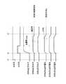
図4は、図2の信号処理回路205a、205b、205cの出力波形を示す図である。画素201aは光を照射して明部にし、画素201b、201cは暗部、もしくは遮光した場合の各信号処理回路205a、205b、205cの出力と図3のA点の電圧VBLの変動を示している。時刻t1に、垂直走査回路から配線202を介して画素201a〜201cの行選択トランジスタ215のゲートにハイレベルの選択パルス信号φ202が供給され、行選択トランジスタ215がオンする。次に、時刻t2に、垂直走査回路から配線203を介して画素201a、201b、201cの転送トランジスタ214のゲートにハイレベルの転送パルス信号φ203が供給され、転送トランジスタ214がオンする。画素201a、201b、201cのフォトダイオード213の画素信号は、信号出力線204a、204b、204cを介してそれぞれ信号処理回路205a、205b、205cに入力される。明部の画素201aに対応する信号処理回路205aの出力OUTが信号の大きさに比例して上昇する。すると、寄生容量219を介して、電圧VBLが与えられている信号処理回路205a〜205cのA点にΔVBLの電位変動が生ずる。この変動は、寄生容量219による、明部の画素201aに対応する信号処理回路205aの出力OUTとA点の容量結合の結果である。即ち、信号処理回路205aの出力OUTの光信号(sig)に応じて、信号処理回路205aの増幅器206のA点の電位がΔVBL変動する。また、信号処理回路205a〜205cは、水平方向に共通の配線で電圧VBLが供給されているため、明部の信号処理回路205aのA点のΔVBLの変動が暗部の信号処理回路205b、205cにも影響する。その結果、信号処理回路205b、205cのA点の電位がΔVBL変動し、その変動が更に暗部の信号処理回路205b、205cの出力OUTを変動させる。この信号処理回路205b、205cの出力OUTの変動は本来の画像信号ではない「偽信号」である。 FIG. 4 is a diagram showing output waveforms of the
電圧VBLを供給する電源回路は、これらの電位変動を抑えるべく電流を引き込み、本来の電圧VBLに戻そうとするが、寄生抵抗218により長い時間を要する(期間t2〜t3)。限られた時間の中で信号処理回路205a〜205cの信号読み出しが完了する場合、A点の電位上昇が残る。暗部の信号処理回路205b、205cでは、A点が電圧上昇すると、トランジスタ1102のゲート−ドレイン間容量219により出力端子OUTの電位が上昇し、本来の暗部信号より明るい偽信号を出力する。信号読み出し時間(期間t2〜t3)を長くすれば、この問題は緩和されるが、駒速やフレームレートが低下する。また、詳細な説明は省略するが、電圧VBHについてもトランジスタ1103及び1104のゲートに寄生抵抗が生じると同じ問題が生じる。 The power supply circuit that supplies the voltage VBL draws a current to suppress these potential fluctuations and tries to return to the original voltage VBL, but takes a longer time due to the parasitic resistance 218 (period t2 to t3). When signal reading of the
図2は画素配列が3×3の場合を例示しているが、実際は図8(A)及び(B)のように数千列×数千行の画素配列になる。図8(A)は入射光の画素領域の様子を示し、画素領域は明部L及び暗部Dを有する。図8(B)は固体撮像装置の出力画像を示し、偽信号Fの画像が生じる。偽信号Fは、明部Lと同じ行の左右の暗部Dで生じる。数千列の信号処理回路205a〜205c等の出力が上昇すると、数千列の寄生容量219による容量結合を受けるので、ΔVBLは非常に大きくなり、偽信号が大きくなる。以上では、A点の電位が上昇する場合の偽信号を例にあげたが、A点の電位が下降する場合、実際の入射光よりも暗い出力を与える偽信号を出力することになる。本実施形態では、カスコード回路を構成するトランジスタ1101及び1102のゲートと電圧VBLを供給する配線の間の寄生抵抗218を低減することで、変動電位ΔVBLを抑制する。 FIG. 2 exemplifies the case where the pixel arrangement is 3 × 3, but in actuality, the pixel arrangement is several thousand columns × thousands rows as shown in FIGS. 8A and 8B. FIG. 8A shows a state of a pixel region of incident light, and the pixel region has a bright portion L and a dark portion D. FIG. 8B shows an output image of the solid-state imaging device, and an image of a false signal F is generated. The false signal F is generated in the left and right dark portions D in the same row as the bright portion L. When the output of the
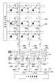
図5は、本実施形態の固体撮像素子102の信号処理回路205a〜205cの増幅器206のパターンレイアウト図である。信号処理回路205a〜205cは、画素201a〜201cから画素信号が読み出される複数の信号出力線204a〜204cに対応して形成され、画素信号を増幅又は信号処理を行う信号処理回路であり、カスコード回路を有する増幅器206を含む。1101G、1102Gはカスコード回路を含むトランジスタ1101、1102のゲート電極であり、ゲート電極と同じ材料であるポリシリコンを主成分とする材料で電気的に接続されている。1105Gはトランジスタ1105の負入力信号IN−の負入力ゲート電極、1106Gはトランジスタ1106の正入力信号IN+の正入力ゲート電極である。402はカスコード回路に供給する電圧VBLを導く導電材料の配線であり、信号処理回路205a〜205cの配列の方向Xに配置されており、複数の信号処理回路205a〜205c内の増幅器206のカスコード回路に供給されている。403は異なる配線層を接続するプラグであり、配線402と404を接続する。404はカスコード回路を構成するトランジスタ1101、1102のゲート電極1101G、1102Gを接続する導電材料の配線であり、配線402とは直交し、別層である。405、406は異なる配線層を接続するプラグであり、配線404とゲート電極1101G、1102Gとを接続する。 FIG. 5 is a pattern layout diagram of the
図6(A)〜(C)は、図5のV−V’断面図である。図6(A)において、407は各種の電圧を供給する導電材料の配線であり、信号処理回路205a〜205cの配列の方向に配置されており、信号処理回路205a〜205cに共通で供給される電源電圧配線として使用される。配線402、403、404、405、406の材料は、ゲート電極1101G、1102Gの材料より抵抗率が小さいものを用いることにより、配線402から低抵抗で電圧VBLをゲート電極1101G、1102Gに供給することができる。その結果、出力端子OUTの変化によって電圧VBLが変動しても短い時間で電荷を充放電し、本来の電圧VBLをカスコード回路に供給することができた。その結果、一部の信号処理回路205aの出力信号による他の信号処理回路205b、205cの出力信号への影響による偽信号を低減でき、入射光を忠実に反映した信号を得ることができた。また、図6(B)のようにプラグ405、406を複数用いても良い。また、図6(C)のように、配線402でゲート電極1101Gと1102Gを接続してもよい。 6A to 6C are V-V ′ cross-sectional views of FIG. 5. In FIG. 6A,
カスコード回路を構成するトランジスタ1101と1102の間には正入力トランジスタ1106が位置することが多く、その場合は図2の基準電圧VREFの配線層407を水平方向に配置することになる。その場合は、図6(A)、(B)のように、配線層402とは異なる配線層403を直交させて、ゲート電極1101G及び1102Gを接続する方法が有効となる。 In many cases, the
また、本実施形態では、トランジスタのゲート電極1101G及び1102Gの材料がポリシリコンである場合を例に説明した。Co、W、Ti、Ni等の金属シリサイドを用いることでソース−ドレイン抵抗を低減する手法がある。これらのシリサイド化では、ポリシリコン抵抗のおよそ数分の1に抵抗が下がる。 In this embodiment, the case where the material of the
一方、本実施形態のように、配線402、403、404、405、406の配線材料としてアルミニウムや銅を用いることにより、ゲート電極1101G及び1102Gのポリシリコンのおよそ千分の一に抵抗を下げることができる。本実施形態の配置、接続形態を採用すれば、ポリシコンでもポリサイドでも材料抵抗の低減効果以上の効果が得られる。 On the other hand, by using aluminum or copper as the wiring material of the
増幅器206は、第1の電界効果トランジスタ1101、第2の電界効果トランジスタ1102及び第1の配線402〜406を有する。第1の電界効果トランジスタ1101のゲート電極1101G及び第2の電界効果トランジスタ1102のゲート電極1102Gは、同一の電圧ノード(VBL)に接続される。第1の配線402〜406は、電圧ノード(VBL)と第1及び第2の電界効果トランジスタ1101、1102のゲート電極1101G、1102Gとの間に接続される。第1及び第2の電界効果トランジスタ1101、1102は、複数の増幅器206が配列される方向Xに対して垂直方向Yに配列される。第1の配線402〜406の材料は、第1及び第2の電界効果トランジスタ1101、1102のゲート電極1101G、1102Gの材料より抵抗率が小さい。 The
第1の配線402〜406は、第2の配線402と、第1のプラグ403と、第3の配線404と、第2のプラグ405と、第3のプラグ406とを有する。第2の配線402は、電圧ノード(VBL)に接続される。第1のプラグ403は、第2の配線402に接続される。第3の配線404は、第1のプラグ403に接続される。第2のプラグ405は、第3の配線404及び第1の電界効果トランジスタ1101のゲート電極1101G間に接続される。第3のプラグ406は、第3の配線404及び第2の電界効果トランジスタ1102のゲート電極1102G間に接続される。第3の配線404上において、第1のプラグ403は、第2のプラグ405と第3のプラグ406との間に配置される。第2の電界効果トランジスタ1102のドレイン又はソースは、増幅器206の出力端子OUTに接続される。第2の電界効果トランジスタ1102のゲート電極1102Gは、寄生容量219により増幅器206の出力端子OUTと容量結合されている。 The
画素面積の縮小化による感度低下を補うために信号処理回路205a〜205cにおいて高ゲインを掛ける手法、或いは図2の容量216及び217の容量比を可変にすることでゲイン切り替え機能を持つ信号処理回路205a〜205cを用いることができる。一般的に、高ゲインの回路は応答性が悪くなり、信号処理時間や読み出し時間が長くなる。そのような状況では、ゲート電極1101G及び1102G間の抵抗が大きいことによって生じるΔVBLの電位変動は、この電位変動を吸収する時間(期間t1〜t3)が大きくなるが故に、高速化の妨げとなる。従って、本実施形態による効果は、多画素化による画素縮小、周辺回路の縮小でより顕著となる。 A signal processing circuit having a gain switching function by applying a high gain in the
(第2の実施形態)
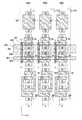
図7は、本発明の第2の実施形態による信号処理回路205a〜205cの増幅器206のパターンレイアウト図である。トランジスタ1101、1102、1105、1106は、櫛歯形状のゲート電極1101G、1102G、1105G、1106Gを有する。これにより、各トランジスタ1101、1102、1105、1106は、複数のトランジスタの並列接続回路で構成されるので、チャネル幅Wを広くし、高いgmを得て、高い開ループゲインを得ることができる。その場合、カスコード回路を構成するトランジスタ1101のゲート電極1101Gとトランジスタ1102のゲート電極1102Gの距離D14がさらに大きくなる為、本実施形態の効果はさらに顕著になる。また、第1の実施形態と同様に、シリサイドゲート材料であっても本実施形態の効果は得られる。(Second Embodiment)
FIG. 7 is a pattern layout diagram of the
第1及び第2の実施形態によれば、信号処理回路205a〜205cのカスコード回路を構成する複数のトランンジスタ1101、1102のゲート電極1101G、1102Gに接続する配線402〜406の抵抗を下げる。これにより、一部の信号処理回路205aの増幅器206の出力信号によって生じる他の信号処理回路205b、205cの増幅器206の偽信号を抑制することができる。 According to the first and second embodiments, the resistances of the
なお、上記実施形態は、何れも本発明を実施するにあたっての具体化の例を示したものに過ぎず、これらによって本発明の技術的範囲が限定的に解釈されてはならないものである。すなわち、本発明はその技術思想、又はその主要な特徴から逸脱することなく、様々な形で実施することができる。 The above-described embodiments are merely examples of implementation in carrying out the present invention, and the technical scope of the present invention should not be construed in a limited manner. That is, the present invention can be implemented in various forms without departing from the technical idea or the main features thereof.
201a〜201c 画素、204a〜204c 信号出力線、206 増幅器、1101〜1106 トランジスタ、1101G〜1106G トランジスタのゲート電極、402,404 配線、403,405,406 プラグ201a to 201c pixel, 204a to 204c signal output line, 206 amplifier, 1101 to 1106 transistor, 1101G to 1106G transistor gate electrode, 402, 404 wiring, 403, 405, 406 plug
Claims (7)
Translated fromJapanese前記複数の画素により生成された画素信号が出力される複数の信号出力線と、
前記信号出力線毎に設けられ、前記複数の信号出力線の画素信号を増幅する複数の増幅器とを有し、
前記増幅器は、
同一の電圧がゲート電極に供給される第1及び第2の電界効果トランジスタと、
前記第1及び第2の電界効果トランジスタのゲート電極を接続する第1の配線と、
前記複数の増幅器に接続される前記第1の配線同士を接続し、前記同一の電圧が供給される共通バイアス配線とを有し、
前記第1及び第2の電界効果トランジスタは、前記複数の増幅器が配列される方向に対して垂直方向に配列され、
前記第1の電界効果トランジスタは、各々のゲート電極が相互に接続される並列接続の複数の第1のトランジスタを有し、
前記第2の電界効果トランジスタは、各々のゲート電極が相互に接続される並列接続の複数の第2のトランジスタを有し、
前記複数の第1のトランジスタ及び前記複数の第2のトランジスは同一線上に並んでおり、
前記第1の配線の材料は、前記第1及び第2の電界効果トランジスタのゲート電極の材料より抵抗率が小さく、
前記第1及び第2の電界効果トランジスタのチャネルは、同一方向に揃っていることを特徴とする固体撮像装置。A plurality of pixels that generate pixel signals by photoelectric conversion;
A plurality of signal output lines for outputting pixel signals generated by the plurality of pixels;
A plurality of amplifiers that are provided for each of the signal output lines and amplify pixel signals of the plurality of signal output lines;
The amplifier is
First and second field effect transistors in which the same voltage is supplied to the gate electrode;
A first wiring connecting gate electrodes of the first and second field effect transistors;
Connecting the first wirings connected to the plurality of amplifiers, and having the common bias wiring to which the same voltage is supplied,
The first and second field effect transistors are arranged in a direction perpendicular to a direction in which the plurality of amplifiers are arranged,
The first field effect transistor has a plurality of first transistors connected in parallel, each gate electrode being connected to each other,
The second field effect transistor has a plurality of parallel-connected second transistors in which the gate electrodes are connected to each other,
The plurality of first transistors and the plurality of second transistors are arranged on the same line,
The material of the first wiring has a lower resistivity than the material of the gate electrodes of the first and second field effect transistors,
A solid-state imaging device, wherein the channels of the first and second field effect transistors are aligned in the same direction.
前記共通バイアス配線に接続される第2の配線と、
前記第2の配線に接続される第1のプラグと、
前記第1のプラグに接続される第3の配線と、
前記第3の配線及び前記第1の電界効果トランジスタのゲート電極間に接続される第2のプラグと、
前記第3の配線及び前記第2の電界効果トランジスタのゲート電極間に接続される第3のプラグとを有することを特徴とする請求項1記載の固体撮像装置。The first wiring is
A second wiring connected to thecommon bias wiring ;
A first plug connected to the second wiring;
A third wiring connected to the first plug;
A second plug connected between the third wiring and the gate electrode of the first field effect transistor;
The solid-state imaging device according to claim 1, further comprising a third plug connected between the third wiring and the gate electrode of the second field effect transistor.
前記第1の入力トランジスタは、前記第2の電界効果トランジスタに直列に接続され、The first input transistor is connected in series to the second field effect transistor;
前記第2の入力トランジスタは、前記第1の電界効果トランジスタに直列に接続され、The second input transistor is connected in series to the first field effect transistor;
前記第1の入力トランジスタ、前記第2の電界効果トランジスタ、前記第2の入力トランジスタ及び前記第1の電界効果トランジスタが、この順に配列され、The first input transistor, the second field effect transistor, the second input transistor, and the first field effect transistor are arranged in this order,
前記第1及び第2の入力トランジスタのチャネルは、前記第1及び第2の電界効果トランジスタのチャネルと同一方向になるように形成されていることを特徴とする請求項1〜6のいずれか1項に記載の固体撮像装置。The channel of the first and second input transistors is formed so as to be in the same direction as the channel of the first and second field effect transistors. The solid-state imaging device according to item.
Priority Applications (2)
| Application Number | Priority Date | Filing Date | Title |
|---|---|---|---|
| JP2010088080AJP5780711B2 (en) | 2010-04-06 | 2010-04-06 | Solid-state imaging device |
| US13/075,259US8520102B2 (en) | 2010-04-06 | 2011-03-30 | Solid-state imaging apparatus |
Applications Claiming Priority (1)
| Application Number | Priority Date | Filing Date | Title |
|---|---|---|---|
| JP2010088080AJP5780711B2 (en) | 2010-04-06 | 2010-04-06 | Solid-state imaging device |
Publications (3)
| Publication Number | Publication Date |
|---|---|
| JP2011222631A JP2011222631A (en) | 2011-11-04 |
| JP2011222631A5 JP2011222631A5 (en) | 2013-05-23 |
| JP5780711B2true JP5780711B2 (en) | 2015-09-16 |
Family
ID=44709251
Family Applications (1)
| Application Number | Title | Priority Date | Filing Date |
|---|---|---|---|
| JP2010088080AExpired - Fee RelatedJP5780711B2 (en) | 2010-04-06 | 2010-04-06 | Solid-state imaging device |
Country Status (2)
| Country | Link |
|---|---|
| US (1) | US8520102B2 (en) |
| JP (1) | JP5780711B2 (en) |
Families Citing this family (24)
| Publication number | Priority date | Publication date | Assignee | Title |
|---|---|---|---|---|
| JP5679653B2 (en) | 2009-12-09 | 2015-03-04 | キヤノン株式会社 | Photoelectric conversion device and imaging system using the same |
| JP5656484B2 (en) | 2010-07-07 | 2015-01-21 | キヤノン株式会社 | Solid-state imaging device and imaging system |
| JP5751766B2 (en) | 2010-07-07 | 2015-07-22 | キヤノン株式会社 | Solid-state imaging device and imaging system |
| JP5643555B2 (en) | 2010-07-07 | 2014-12-17 | キヤノン株式会社 | Solid-state imaging device and imaging system |
| JP5697371B2 (en) | 2010-07-07 | 2015-04-08 | キヤノン株式会社 | Solid-state imaging device and imaging system |
| JP5885401B2 (en) | 2010-07-07 | 2016-03-15 | キヤノン株式会社 | Solid-state imaging device and imaging system |
| JP5645513B2 (en) | 2010-07-07 | 2014-12-24 | キヤノン株式会社 | Solid-state imaging device and imaging system |
| JP5737971B2 (en) | 2011-01-28 | 2015-06-17 | キヤノン株式会社 | Solid-state imaging device and camera |
| JP5744545B2 (en) | 2011-01-31 | 2015-07-08 | キヤノン株式会社 | Solid-state imaging device and camera |
| JP5864990B2 (en) | 2011-10-03 | 2016-02-17 | キヤノン株式会社 | Solid-state imaging device and camera |
| JP6023437B2 (en) | 2012-02-29 | 2016-11-09 | キヤノン株式会社 | Solid-state imaging device and camera |
| JP6108884B2 (en) | 2013-03-08 | 2017-04-05 | キヤノン株式会社 | Photoelectric conversion device and imaging system |
| JP2014175553A (en) | 2013-03-11 | 2014-09-22 | Canon Inc | Solid-state imaging device and camera |
| JP6541347B2 (en) | 2014-03-27 | 2019-07-10 | キヤノン株式会社 | Solid-state imaging device and imaging system |
| JP6548391B2 (en) | 2014-03-31 | 2019-07-24 | キヤノン株式会社 | Photoelectric conversion device and imaging system |
| JP6313652B2 (en)* | 2014-05-19 | 2018-04-18 | オリンパス株式会社 | Image sensor |
| US9900539B2 (en) | 2015-09-10 | 2018-02-20 | Canon Kabushiki Kaisha | Solid-state image pickup element, and image pickup system |
| JP6732468B2 (en) | 2016-02-16 | 2020-07-29 | キヤノン株式会社 | Photoelectric conversion device and driving method thereof |
| JP6740067B2 (en) | 2016-09-16 | 2020-08-12 | キヤノン株式会社 | Solid-state imaging device and driving method thereof |
| JP6750876B2 (en) | 2016-10-07 | 2020-09-02 | キヤノン株式会社 | Solid-state imaging device and driving method thereof |
| JP7046551B2 (en)* | 2017-10-03 | 2022-04-04 | キヤノン株式会社 | Solid-state image sensor and image sensor |
| JP7214454B2 (en) | 2018-12-06 | 2023-01-30 | キヤノン株式会社 | Photoelectric conversion element and imaging device |
| JP7336206B2 (en) | 2019-02-27 | 2023-08-31 | キヤノン株式会社 | Method for manufacturing photoelectric conversion device |
| JP2023124491A (en) | 2022-02-25 | 2023-09-06 | キヤノン株式会社 | Photoelectric conversion device |
Family Cites Families (64)
| Publication number | Priority date | Publication date | Assignee | Title |
|---|---|---|---|---|
| GB2262658B (en) | 1989-02-21 | 1993-09-29 | Canon Kk | Photoelectric converter |
| JP3067435B2 (en) | 1992-12-24 | 2000-07-17 | キヤノン株式会社 | Image reading photoelectric conversion device and image processing apparatus having the device |
| JPH08186241A (en) | 1995-01-06 | 1996-07-16 | Canon Inc | Imaging element and solid-state imaging device |
| TW421962B (en) | 1997-09-29 | 2001-02-11 | Canon Kk | Image sensing device using mos type image sensing elements |
| JPH11261046A (en) | 1998-03-12 | 1999-09-24 | Canon Inc | Solid-state imaging device |
| JP3571909B2 (en) | 1998-03-19 | 2004-09-29 | キヤノン株式会社 | Solid-state imaging device and method of manufacturing the same |
| US7324144B1 (en) | 1999-10-05 | 2008-01-29 | Canon Kabushiki Kaisha | Solid image pickup device, image pickup system and method of driving solid image pickup device |
| JP3467013B2 (en) | 1999-12-06 | 2003-11-17 | キヤノン株式会社 | Solid-state imaging device |
| JP3728260B2 (en) | 2002-02-27 | 2005-12-21 | キヤノン株式会社 | Photoelectric conversion device and imaging device |
| EP1341377B1 (en) | 2002-02-27 | 2018-04-11 | Canon Kabushiki Kaisha | Signal processing device for image pickup apparatus |
| US20040090254A1 (en)* | 2002-11-13 | 2004-05-13 | Owens Ronnie Edward | Systems and methods for altering timing edges of an input signal |
| TW200518345A (en)* | 2003-08-08 | 2005-06-01 | Renesas Tech Corp | Semiconductor device |
| US7046284B2 (en)* | 2003-09-30 | 2006-05-16 | Innovative Technology Licensing Llc | CMOS imaging system with low fixed pattern noise |
| JP4018644B2 (en) | 2004-01-29 | 2007-12-05 | キヤノン株式会社 | Photoelectric conversion device and imaging system using the same |
| US7605415B2 (en) | 2004-06-07 | 2009-10-20 | Canon Kabushiki Kaisha | Image pickup device comprising photoelectric conversation unit, floating diffusion region and guard ring |
| JP2006042302A (en)* | 2004-06-22 | 2006-02-09 | Matsushita Electric Ind Co Ltd | Solid-state image sensor and camera |
| JP4455435B2 (en) | 2004-08-04 | 2010-04-21 | キヤノン株式会社 | Solid-state imaging device and camera using the solid-state imaging device |
| JP2006073736A (en) | 2004-09-01 | 2006-03-16 | Canon Inc | Photoelectric conversion device, solid-state imaging device, and solid-state imaging system |
| JP4916101B2 (en) | 2004-09-01 | 2012-04-11 | キヤノン株式会社 | Photoelectric conversion device, solid-state imaging device, and solid-state imaging system |
| JP5089017B2 (en) | 2004-09-01 | 2012-12-05 | キヤノン株式会社 | Solid-state imaging device and solid-state imaging system |
| JP4756839B2 (en) | 2004-09-01 | 2011-08-24 | キヤノン株式会社 | Solid-state imaging device and camera |
| JP4971586B2 (en) | 2004-09-01 | 2012-07-11 | キヤノン株式会社 | Solid-state imaging device |
| JP2006197392A (en) | 2005-01-14 | 2006-07-27 | Canon Inc | Solid-state imaging device, camera, and driving method of solid-state imaging device |
| JP4416668B2 (en) | 2005-01-14 | 2010-02-17 | キヤノン株式会社 | Solid-state imaging device, control method thereof, and camera |
| JP4459064B2 (en) | 2005-01-14 | 2010-04-28 | キヤノン株式会社 | Solid-state imaging device, control method thereof, and camera |
| JP4459099B2 (en) | 2005-03-18 | 2010-04-28 | キヤノン株式会社 | Solid-state imaging device and camera |
| JP4677258B2 (en) | 2005-03-18 | 2011-04-27 | キヤノン株式会社 | Solid-state imaging device and camera |
| JP4794877B2 (en) | 2005-03-18 | 2011-10-19 | キヤノン株式会社 | Solid-state imaging device and camera |
| JP4459098B2 (en) | 2005-03-18 | 2010-04-28 | キヤノン株式会社 | Solid-state imaging device and camera |
| US7541628B2 (en)* | 2005-07-09 | 2009-06-02 | Samsung Electronics Co., Ltd. | Image sensors including active pixel sensor arrays |
| JP4827508B2 (en) | 2005-12-02 | 2011-11-30 | キヤノン株式会社 | Imaging system |
| JP4804254B2 (en) | 2006-07-26 | 2011-11-02 | キヤノン株式会社 | Photoelectric conversion device and imaging device |
| JP4194633B2 (en) | 2006-08-08 | 2008-12-10 | キヤノン株式会社 | Imaging apparatus and imaging system |
| JP4185949B2 (en) | 2006-08-08 | 2008-11-26 | キヤノン株式会社 | Photoelectric conversion device and imaging device |
| JP4933199B2 (en)* | 2006-08-31 | 2012-05-16 | キヤノン株式会社 | Solid-state imaging device and imaging system |
| JP4928199B2 (en) | 2006-09-07 | 2012-05-09 | キヤノン株式会社 | Signal detection device, signal readout method of signal detection device, and imaging system using signal detection device |
| JP5043388B2 (en) | 2006-09-07 | 2012-10-10 | キヤノン株式会社 | Solid-state imaging device and imaging system |
| JP5173171B2 (en) | 2006-09-07 | 2013-03-27 | キヤノン株式会社 | PHOTOELECTRIC CONVERSION DEVICE, IMAGING DEVICE, AND SIGNAL READING METHOD |
| JP4054839B1 (en) | 2007-03-02 | 2008-03-05 | キヤノン株式会社 | Photoelectric conversion device and imaging system using the same |
| JP5053737B2 (en) | 2007-07-06 | 2012-10-17 | キヤノン株式会社 | Photoelectric conversion device |
| EP2037667B1 (en) | 2007-09-14 | 2017-08-23 | Canon Kabushiki Kaisha | Image sensing apparatus and imaging system |
| JP2009094571A (en)* | 2007-10-03 | 2009-04-30 | Toshiba Corp | Semiconductor integrated circuit |
| JP5164509B2 (en) | 2007-10-03 | 2013-03-21 | キヤノン株式会社 | Photoelectric conversion device, photoelectric conversion device for visible light, and imaging system using them |
| US7940121B2 (en)* | 2007-12-19 | 2011-05-10 | Panasonic Corporation | Operational amplifier and pipeline AD converter |
| JP5142696B2 (en) | 2007-12-20 | 2013-02-13 | キヤノン株式会社 | Photoelectric conversion device and imaging system using photoelectric conversion device |
| JP5142749B2 (en) | 2008-02-14 | 2013-02-13 | キヤノン株式会社 | IMAGING DEVICE, IMAGING DEVICE CONTROL METHOD, AND IMAGING SYSTEM |
| JP5268389B2 (en) | 2008-02-28 | 2013-08-21 | キヤノン株式会社 | Solid-state imaging device, driving method thereof, and imaging system |
| JP5213501B2 (en) | 2008-04-09 | 2013-06-19 | キヤノン株式会社 | Solid-state imaging device |
| JP4494492B2 (en) | 2008-04-09 | 2010-06-30 | キヤノン株式会社 | Solid-state imaging device and driving method of solid-state imaging device |
| JP5328224B2 (en) | 2008-05-01 | 2013-10-30 | キヤノン株式会社 | Solid-state imaging device |
| JP4759590B2 (en) | 2008-05-09 | 2011-08-31 | キヤノン株式会社 | Photoelectric conversion device and imaging system using the same |
| JP2009278241A (en) | 2008-05-13 | 2009-11-26 | Canon Inc | Drive method of solid-state image pickup device, and solid-state image pickup device |
| JP5161676B2 (en) | 2008-07-07 | 2013-03-13 | キヤノン株式会社 | Imaging apparatus and imaging system |
| JP5371330B2 (en) | 2008-08-29 | 2013-12-18 | キヤノン株式会社 | Solid-state imaging device |
| JP5288955B2 (en) | 2008-09-09 | 2013-09-11 | キヤノン株式会社 | Solid-state imaging device, imaging system, and driving method of solid-state imaging device |
| JP5274166B2 (en) | 2008-09-10 | 2013-08-28 | キヤノン株式会社 | Photoelectric conversion device and imaging system |
| JP5264379B2 (en) | 2008-09-12 | 2013-08-14 | キヤノン株式会社 | IMAGING DEVICE, IMAGING SYSTEM, AND OPERATION METHOD OF IMAGING DEVICE |
| JP5258551B2 (en) | 2008-12-26 | 2013-08-07 | キヤノン株式会社 | Solid-state imaging device, driving method thereof, and imaging system |
| JP5478905B2 (en) | 2009-01-30 | 2014-04-23 | キヤノン株式会社 | Solid-state imaging device |
| JP5558857B2 (en) | 2009-03-09 | 2014-07-23 | キヤノン株式会社 | Photoelectric conversion device and imaging system using the same |
| JP5529613B2 (en) | 2009-04-17 | 2014-06-25 | キヤノン株式会社 | Photoelectric conversion device and imaging system |
| JP4881987B2 (en) | 2009-10-06 | 2012-02-22 | キヤノン株式会社 | Solid-state imaging device and imaging device |
| JP5290923B2 (en) | 2009-10-06 | 2013-09-18 | キヤノン株式会社 | Solid-state imaging device and imaging device |
| JP5679653B2 (en) | 2009-12-09 | 2015-03-04 | キヤノン株式会社 | Photoelectric conversion device and imaging system using the same |
- 2010
- 2010-04-06JPJP2010088080Apatent/JP5780711B2/ennot_activeExpired - Fee Related
- 2011
- 2011-03-30USUS13/075,259patent/US8520102B2/ennot_activeExpired - Fee Related
Also Published As
| Publication number | Publication date |
|---|---|
| US8520102B2 (en) | 2013-08-27 |
| US20110242380A1 (en) | 2011-10-06 |
| JP2011222631A (en) | 2011-11-04 |
Similar Documents
| Publication | Publication Date | Title |
|---|---|---|
| JP5780711B2 (en) | Solid-state imaging device | |
| US10404933B2 (en) | Solid-state imaging apparatus and imaging system | |
| US8081245B2 (en) | Image sensing apparatus and imaging system | |
| CN106993141B (en) | Image pickup apparatus | |
| JP5358136B2 (en) | Solid-state imaging device | |
| KR100657863B1 (en) | Complementary Metal Oxide Semiconductor Active Pixel Sensor Using Fingered Source Follower Transistor | |
| JP5959829B2 (en) | Solid-state imaging device | |
| US9838636B2 (en) | Image pickup apparatus, image pickup system, and method of driving image pickup apparatus | |
| US9053996B2 (en) | Solid-state imaging apparatus with a plurality of processing portions | |
| JP5813047B2 (en) | Imaging device and imaging system. | |
| US20130201372A1 (en) | Photo-electric conversion device and image capturing system | |
| CN104243862B (en) | Solid state image sensor | |
| JP6238558B2 (en) | Imaging device and imaging system. | |
| JP4051034B2 (en) | Amplification type solid-state imaging device and driving method thereof | |
| US9426391B2 (en) | Solid-state imaging apparatus, method of controlling the same, and imaging system | |
| JP2018093298A (en) | Photoelectric conversion device and photoelectric conversion system | |
| JP5219555B2 (en) | IMAGING DEVICE AND IMAGING SYSTEM USING IMAGING DEVICE | |
| JP2013197989A (en) | Solid state image pickup device | |
| JP2008060269A (en) | Photoelectric conversion device and imaging device | |
| JP6370135B2 (en) | Imaging device, imaging system, and driving method of imaging device | |
| JP7330124B2 (en) | Solid-state imaging device | |
| US20160156870A1 (en) | Solid-state imaging device | |
| JP2017188842A (en) | Solid-state imaging device and imaging system | |
| JP4746962B2 (en) | Solid-state imaging device and imaging system | |
| JP6796166B2 (en) | Imaging device, imaging system, and driving method of imaging device |
Legal Events
| Date | Code | Title | Description |
|---|---|---|---|
| A521 | Request for written amendment filed | Free format text:JAPANESE INTERMEDIATE CODE: A523 Effective date:20130405 | |
| A621 | Written request for application examination | Free format text:JAPANESE INTERMEDIATE CODE: A621 Effective date:20130405 | |
| A977 | Report on retrieval | Free format text:JAPANESE INTERMEDIATE CODE: A971007 Effective date:20140205 | |
| A131 | Notification of reasons for refusal | Free format text:JAPANESE INTERMEDIATE CODE: A131 Effective date:20140218 | |
| A521 | Request for written amendment filed | Free format text:JAPANESE INTERMEDIATE CODE: A523 Effective date:20140417 | |
| A131 | Notification of reasons for refusal | Free format text:JAPANESE INTERMEDIATE CODE: A131 Effective date:20141202 | |
| A521 | Request for written amendment filed | Free format text:JAPANESE INTERMEDIATE CODE: A523 Effective date:20150129 | |
| TRDD | Decision of grant or rejection written | ||
| A01 | Written decision to grant a patent or to grant a registration (utility model) | Free format text:JAPANESE INTERMEDIATE CODE: A01 Effective date:20150616 | |
| A61 | First payment of annual fees (during grant procedure) | Free format text:JAPANESE INTERMEDIATE CODE: A61 Effective date:20150714 | |
| LAPS | Cancellation because of no payment of annual fees |