JP5778899B2 - Backlight assembly - Google Patents
Backlight assemblyDownload PDFInfo
- Publication number
- JP5778899B2 JP5778899B2JP2010162578AJP2010162578AJP5778899B2JP 5778899 B2JP5778899 B2JP 5778899B2JP 2010162578 AJP2010162578 AJP 2010162578AJP 2010162578 AJP2010162578 AJP 2010162578AJP 5778899 B2JP5778899 B2JP 5778899B2
- Authority
- JP
- Japan
- Prior art keywords
- light
- guide plate
- protrusion
- light guide
- backlight assembly
- Prior art date
- Legal status (The legal status is an assumption and is not a legal conclusion. Google has not performed a legal analysis and makes no representation as to the accuracy of the status listed.)
- Active
Links
Images


Classifications
- G—PHYSICS
- G02—OPTICS
- G02B—OPTICAL ELEMENTS, SYSTEMS OR APPARATUS
- G02B6/00—Light guides; Structural details of arrangements comprising light guides and other optical elements, e.g. couplings
- G02B6/0001—Light guides; Structural details of arrangements comprising light guides and other optical elements, e.g. couplings specially adapted for lighting devices or systems
- G02B6/0011—Light guides; Structural details of arrangements comprising light guides and other optical elements, e.g. couplings specially adapted for lighting devices or systems the light guides being planar or of plate-like form
- G02B6/0033—Means for improving the coupling-out of light from the light guide
- G02B6/0035—Means for improving the coupling-out of light from the light guide provided on the surface of the light guide or in the bulk of it
- G02B6/0038—Linear indentations or grooves, e.g. arc-shaped grooves or meandering grooves, extending over the full length or width of the light guide
- G—PHYSICS
- G02—OPTICS
- G02F—OPTICAL DEVICES OR ARRANGEMENTS FOR THE CONTROL OF LIGHT BY MODIFICATION OF THE OPTICAL PROPERTIES OF THE MEDIA OF THE ELEMENTS INVOLVED THEREIN; NON-LINEAR OPTICS; FREQUENCY-CHANGING OF LIGHT; OPTICAL LOGIC ELEMENTS; OPTICAL ANALOGUE/DIGITAL CONVERTERS
- G02F1/00—Devices or arrangements for the control of the intensity, colour, phase, polarisation or direction of light arriving from an independent light source, e.g. switching, gating or modulating; Non-linear optics
- G02F1/01—Devices or arrangements for the control of the intensity, colour, phase, polarisation or direction of light arriving from an independent light source, e.g. switching, gating or modulating; Non-linear optics for the control of the intensity, phase, polarisation or colour
- G02F1/13—Devices or arrangements for the control of the intensity, colour, phase, polarisation or direction of light arriving from an independent light source, e.g. switching, gating or modulating; Non-linear optics for the control of the intensity, phase, polarisation or colour based on liquid crystals, e.g. single liquid crystal display cells
- G02F1/133—Constructional arrangements; Operation of liquid crystal cells; Circuit arrangements
- G02F1/1333—Constructional arrangements; Manufacturing methods
- F—MECHANICAL ENGINEERING; LIGHTING; HEATING; WEAPONS; BLASTING
- F21—LIGHTING
- F21K—NON-ELECTRIC LIGHT SOURCES USING LUMINESCENCE; LIGHT SOURCES USING ELECTROCHEMILUMINESCENCE; LIGHT SOURCES USING CHARGES OF COMBUSTIBLE MATERIAL; LIGHT SOURCES USING SEMICONDUCTOR DEVICES AS LIGHT-GENERATING ELEMENTS; LIGHT SOURCES NOT OTHERWISE PROVIDED FOR
- F21K9/00—Light sources using semiconductor devices as light-generating elements, e.g. using light-emitting diodes [LED] or lasers
- F21K9/60—Optical arrangements integrated in the light source, e.g. for improving the colour rendering index or the light extraction
- F21K9/61—Optical arrangements integrated in the light source, e.g. for improving the colour rendering index or the light extraction using light guides
- G—PHYSICS
- G02—OPTICS
- G02B—OPTICAL ELEMENTS, SYSTEMS OR APPARATUS
- G02B6/00—Light guides; Structural details of arrangements comprising light guides and other optical elements, e.g. couplings
- G02B6/0001—Light guides; Structural details of arrangements comprising light guides and other optical elements, e.g. couplings specially adapted for lighting devices or systems
- G02B6/0011—Light guides; Structural details of arrangements comprising light guides and other optical elements, e.g. couplings specially adapted for lighting devices or systems the light guides being planar or of plate-like form
- G02B6/0066—Light guides; Structural details of arrangements comprising light guides and other optical elements, e.g. couplings specially adapted for lighting devices or systems the light guides being planar or of plate-like form characterised by the light source being coupled to the light guide
- G02B6/0068—Arrangements of plural sources, e.g. multi-colour light sources
- G—PHYSICS
- G02—OPTICS
- G02B—OPTICAL ELEMENTS, SYSTEMS OR APPARATUS
- G02B6/00—Light guides; Structural details of arrangements comprising light guides and other optical elements, e.g. couplings
- G02B6/0001—Light guides; Structural details of arrangements comprising light guides and other optical elements, e.g. couplings specially adapted for lighting devices or systems
- G02B6/0011—Light guides; Structural details of arrangements comprising light guides and other optical elements, e.g. couplings specially adapted for lighting devices or systems the light guides being planar or of plate-like form
- G02B6/0066—Light guides; Structural details of arrangements comprising light guides and other optical elements, e.g. couplings specially adapted for lighting devices or systems the light guides being planar or of plate-like form characterised by the light source being coupled to the light guide
- G02B6/0073—Light emitting diode [LED]
- G—PHYSICS
- G02—OPTICS
- G02B—OPTICAL ELEMENTS, SYSTEMS OR APPARATUS
- G02B6/00—Light guides; Structural details of arrangements comprising light guides and other optical elements, e.g. couplings
- G02B6/0001—Light guides; Structural details of arrangements comprising light guides and other optical elements, e.g. couplings specially adapted for lighting devices or systems
- G02B6/0011—Light guides; Structural details of arrangements comprising light guides and other optical elements, e.g. couplings specially adapted for lighting devices or systems the light guides being planar or of plate-like form
- G02B6/0081—Mechanical or electrical aspects of the light guide and light source in the lighting device peculiar to the adaptation to planar light guides, e.g. concerning packaging
- G02B6/0083—Details of electrical connections of light sources to drivers, circuit boards, or the like
- G—PHYSICS
- G02—OPTICS
- G02B—OPTICAL ELEMENTS, SYSTEMS OR APPARATUS
- G02B6/00—Light guides; Structural details of arrangements comprising light guides and other optical elements, e.g. couplings
- G02B6/0001—Light guides; Structural details of arrangements comprising light guides and other optical elements, e.g. couplings specially adapted for lighting devices or systems
- G02B6/0011—Light guides; Structural details of arrangements comprising light guides and other optical elements, e.g. couplings specially adapted for lighting devices or systems the light guides being planar or of plate-like form
- G02B6/0081—Mechanical or electrical aspects of the light guide and light source in the lighting device peculiar to the adaptation to planar light guides, e.g. concerning packaging
- G02B6/0085—Means for removing heat created by the light source from the package
- G—PHYSICS
- G02—OPTICS
- G02B—OPTICAL ELEMENTS, SYSTEMS OR APPARATUS
- G02B6/00—Light guides; Structural details of arrangements comprising light guides and other optical elements, e.g. couplings
- G02B6/0001—Light guides; Structural details of arrangements comprising light guides and other optical elements, e.g. couplings specially adapted for lighting devices or systems
- G02B6/0011—Light guides; Structural details of arrangements comprising light guides and other optical elements, e.g. couplings specially adapted for lighting devices or systems the light guides being planar or of plate-like form
- G02B6/0081—Mechanical or electrical aspects of the light guide and light source in the lighting device peculiar to the adaptation to planar light guides, e.g. concerning packaging
- G02B6/0086—Positioning aspects
- G02B6/0088—Positioning aspects of the light guide or other optical sheets in the package
- G—PHYSICS
- G02—OPTICS
- G02B—OPTICAL ELEMENTS, SYSTEMS OR APPARATUS
- G02B6/00—Light guides; Structural details of arrangements comprising light guides and other optical elements, e.g. couplings
- G02B6/0001—Light guides; Structural details of arrangements comprising light guides and other optical elements, e.g. couplings specially adapted for lighting devices or systems
- G02B6/0011—Light guides; Structural details of arrangements comprising light guides and other optical elements, e.g. couplings specially adapted for lighting devices or systems the light guides being planar or of plate-like form
- G02B6/0081—Mechanical or electrical aspects of the light guide and light source in the lighting device peculiar to the adaptation to planar light guides, e.g. concerning packaging
- G02B6/0086—Positioning aspects
- G02B6/0091—Positioning aspects of the light source relative to the light guide
- G—PHYSICS
- G02—OPTICS
- G02F—OPTICAL DEVICES OR ARRANGEMENTS FOR THE CONTROL OF LIGHT BY MODIFICATION OF THE OPTICAL PROPERTIES OF THE MEDIA OF THE ELEMENTS INVOLVED THEREIN; NON-LINEAR OPTICS; FREQUENCY-CHANGING OF LIGHT; OPTICAL LOGIC ELEMENTS; OPTICAL ANALOGUE/DIGITAL CONVERTERS
- G02F1/00—Devices or arrangements for the control of the intensity, colour, phase, polarisation or direction of light arriving from an independent light source, e.g. switching, gating or modulating; Non-linear optics
- G02F1/01—Devices or arrangements for the control of the intensity, colour, phase, polarisation or direction of light arriving from an independent light source, e.g. switching, gating or modulating; Non-linear optics for the control of the intensity, phase, polarisation or colour
- G02F1/13—Devices or arrangements for the control of the intensity, colour, phase, polarisation or direction of light arriving from an independent light source, e.g. switching, gating or modulating; Non-linear optics for the control of the intensity, phase, polarisation or colour based on liquid crystals, e.g. single liquid crystal display cells
- G02F1/133—Constructional arrangements; Operation of liquid crystal cells; Circuit arrangements
- G02F1/1333—Constructional arrangements; Manufacturing methods
- G02F1/1335—Structural association of cells with optical devices, e.g. polarisers or reflectors
- G02F1/1336—Illuminating devices
- G02F1/133615—Edge-illuminating devices, i.e. illuminating from the side
- F—MECHANICAL ENGINEERING; LIGHTING; HEATING; WEAPONS; BLASTING
- F21—LIGHTING
- F21Y—INDEXING SCHEME ASSOCIATED WITH SUBCLASSES F21K, F21L, F21S and F21V, RELATING TO THE FORM OR THE KIND OF THE LIGHT SOURCES OR OF THE COLOUR OF THE LIGHT EMITTED
- F21Y2115/00—Light-generating elements of semiconductor light sources
- F21Y2115/10—Light-emitting diodes [LED]
- G—PHYSICS
- G02—OPTICS
- G02F—OPTICAL DEVICES OR ARRANGEMENTS FOR THE CONTROL OF LIGHT BY MODIFICATION OF THE OPTICAL PROPERTIES OF THE MEDIA OF THE ELEMENTS INVOLVED THEREIN; NON-LINEAR OPTICS; FREQUENCY-CHANGING OF LIGHT; OPTICAL LOGIC ELEMENTS; OPTICAL ANALOGUE/DIGITAL CONVERTERS
- G02F2201/00—Constructional arrangements not provided for in groups G02F1/00 - G02F7/00
- G02F2201/46—Fixing elements
- G—PHYSICS
- G02—OPTICS
- G02F—OPTICAL DEVICES OR ARRANGEMENTS FOR THE CONTROL OF LIGHT BY MODIFICATION OF THE OPTICAL PROPERTIES OF THE MEDIA OF THE ELEMENTS INVOLVED THEREIN; NON-LINEAR OPTICS; FREQUENCY-CHANGING OF LIGHT; OPTICAL LOGIC ELEMENTS; OPTICAL ANALOGUE/DIGITAL CONVERTERS
- G02F2201/00—Constructional arrangements not provided for in groups G02F1/00 - G02F7/00
- G02F2201/54—Arrangements for reducing warping-twist
- G—PHYSICS
- G02—OPTICS
- G02F—OPTICAL DEVICES OR ARRANGEMENTS FOR THE CONTROL OF LIGHT BY MODIFICATION OF THE OPTICAL PROPERTIES OF THE MEDIA OF THE ELEMENTS INVOLVED THEREIN; NON-LINEAR OPTICS; FREQUENCY-CHANGING OF LIGHT; OPTICAL LOGIC ELEMENTS; OPTICAL ANALOGUE/DIGITAL CONVERTERS
- G02F2203/00—Function characteristic
- G02F2203/60—Temperature independent
Landscapes
- Physics & Mathematics (AREA)
- Optics & Photonics (AREA)
- General Physics & Mathematics (AREA)
- Nonlinear Science (AREA)
- Engineering & Computer Science (AREA)
- Mathematical Physics (AREA)
- Chemical & Material Sciences (AREA)
- Crystallography & Structural Chemistry (AREA)
- Microelectronics & Electronic Packaging (AREA)
- General Engineering & Computer Science (AREA)
- Planar Illumination Modules (AREA)
- Liquid Crystal (AREA)
Description
Translated fromJapanese本発明は、バックライトアセンブリに関し、より詳しくは光効率を向上させ、均一な表示輝度を維持するバックライトアセンブリに関する。 The present invention relates to a backlight assembly, and more particularly to a backlight assembly that improves light efficiency and maintains uniform display brightness.
液晶表示装置(Liquid Crystal Display:LCD)は、現在最も幅広く使用されている平板表示装置(Flat Panel Display)のうちの一つとして、電極が形成されている2枚の基板とその間に挿入されている液晶層(liquid crystal:LC)からなって、電極に電圧を印加して液晶層の液晶分子の配列を制御して透過する光の量を調節する表示装置である。 A liquid crystal display (LCD) is one of the most widely used flat panel displays (Flat Panel Display), and is inserted between two substrates on which electrodes are formed and between them. The liquid crystal layer (liquid crystal: LC) is a display device that adjusts the amount of light transmitted by applying a voltage to an electrode to control the arrangement of liquid crystal molecules in the liquid crystal layer.
このような液晶分子は、印加される電場の方向及び強さによって光透過率を変更して画像を表示するため、液晶表示装置は、画像を表示するための光を必要とする。液晶表示装置に使用される光源としては、発光ダイオード(Light Emitting Diode:LED)、冷陰極蛍光ランプ(Cold Cathode Fluorescent Lamp:CCFL)、平板蛍光ランプ(Flat Fluorescent Lamp:FFL)などが代表的である。 Since such liquid crystal molecules display an image by changing the light transmittance according to the direction and intensity of the applied electric field, the liquid crystal display device requires light for displaying the image. Typical examples of the light source used in the liquid crystal display device include a light emitting diode (LED), a cold cathode fluorescent lamp (CCFL), a flat fluorescent lamp (FFL), and the like. .
従来の液晶表示装置には発光ダイオードを利用した導光板(light guide plate:LGP)の側面から光を照射するエッジ型バックライトアセンブリが利用されてきた。このような側面照射方式の場合、発光ダイオードの上面と導光板の側面までの距離、つまり、入光距離が周囲温度及び湿度などの環境に応じて変わる導光板自体の伸縮性によって均一に維持されない問題がある。 In the conventional liquid crystal display device, an edge type backlight assembly that irradiates light from a side surface of a light guide plate (LGP) using a light emitting diode has been used. In the case of such a side illumination method, the distance between the upper surface of the light emitting diode and the side surface of the light guide plate, that is, the light incident distance is not uniformly maintained due to the stretchability of the light guide plate itself that changes according to the environment such as ambient temperature and humidity. There's a problem.
本発明が解決しようとする課題は、発光ダイオードの上面と導光板の側面までの距離を一定に維持するエッジ型バックライトアセンブリを提供することである。 The problem to be solved by the present invention is to provide an edge type backlight assembly that maintains a constant distance between the upper surface of the light emitting diode and the side surface of the light guide plate.
上述の課題を達成するための本発明の一実施形態に係るバックライトアセンブリは、複数の点光源、導光板、及び印刷回路基板を含む。点光源は光を出射し、第1方向に沿って配列される。導光板は点光源から出射する光が入射される入光面、入光面の縁から延長し形成された側面及び側面から導光板内部方向に沿って形成される固定溝を有する。印刷回路基板(PCB)は、複数の点光源が配置された点光源配置部と、点光源配置部から第1方向と実質的に垂直する第2方向に延長し形成された延長部、延長部の縁に固定される突起を有する。印刷回路基板の突起は、導光板の固定溝と結合される。 To achieve the above object, a backlight assembly according to an embodiment of the present invention includes a plurality of point light sources, a light guide plate, and a printed circuit board. The point light sources emit light and are arranged along the first direction. The light guide plate has a light incident surface on which light emitted from the point light source is incident, a side surface extending from the edge of the light incident surface, and a fixed groove formed along the inner direction of the light guide plate from the side surface. A printed circuit board (PCB) includes a point light source arrangement portion in which a plurality of point light sources are arranged, an extension portion formed by extending from the point light source arrangement portion in a second direction substantially perpendicular to the first direction, and an extension portion A protrusion fixed to the edge of the substrate. The protrusion of the printed circuit board is coupled to the fixing groove of the light guide plate.
上述の課題を達成するための本発明の他の実施形態に係るバックライトアセンブリは複数の光源、光源モジュールカバー、導光板、及び収納容器を含む。点光源は、第1方向に光を出射する。光源モジュールカバーは、点光源を固定する光源固定部、光源固定部から一側に延長し形成された延長部及び延長部に形成された導光板固定部を含む。導光板は複数の光源から第1方向に近接して配置される光入射面、光入射面の短辺から第1方向に延長し形成される側面、光入射面の長辺から第1方向に延長し形成される光出射面、光出射面の反対側に形成されて光入射面から入射された光が拡散及び反射される光反射面を有する。収納容器は光源モジュールカバーと導光板を支持する底板、底板の縁で曲げられた側壁を含む。この場合、導光板の側面には光源モジュールカバーの導光板固定部を収容する固定溝が形成されており、光源モジュールカバーは導光板とオーバーラップし配置され、収納容器の底板と独立的に流動する。 A backlight assembly according to another embodiment of the present invention for achieving the above-described problems includes a plurality of light sources, a light source module cover, a light guide plate, and a receiving container. The point light source emits light in the first direction. The light source module cover includes a light source fixing part for fixing the point light source, an extension part extending from the light source fixing part to one side, and a light guide plate fixing part formed on the extension part. The light guide plate is a light incident surface disposed in the vicinity of the first direction from a plurality of light sources, a side surface formed by extending the short side of the light incident surface in the first direction, and the long side of the light incident surface in the first direction. An extended light output surface, and a light reflection surface that is formed on the opposite side of the light output surface and diffuses and reflects light incident from the light incident surface. The storage container includes a light source module cover and a bottom plate supporting the light guide plate, and a side wall bent at an edge of the bottom plate. In this case, a fixing groove for receiving the light guide plate fixing portion of the light source module cover is formed on the side surface of the light guide plate, and the light source module cover is disposed so as to overlap the light guide plate and flows independently from the bottom plate of the storage container. To do.
その他の実施形態の具体的な事項は詳しい説明及び図面に含まれている。 Specific details of other embodiments are included in the detailed description and drawings.
以下、図1〜図14を参照して、本発明の実施形態について詳しく説明する。 Hereinafter, embodiments of the present invention will be described in detail with reference to FIGS.
図1は、従来のエッジ型バックライトアセンブリ191を含む液晶表示装置100を示す斜視図である。図2は、図1の液晶表示装置のI−I’線に沿って切断した断面図である。 FIG. 1 is a perspective view showing a liquid
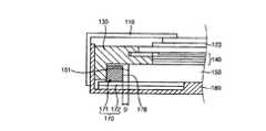
図1及び図2を参照すると、導光板(Light Guide Plate:LGP)150は、光源モジュール170から発生される光を入射する入光面151、入光面151と対向する対向面152、入光面151と対向する対向面152と接続し、液晶表示パネルに沿って光が出射される出光面153及び出光面153と対向し配置される反射面154を含む。 Referring to FIGS. 1 and 2, a light guide plate (LGP) 150 includes a
導光板150は、一側面に配置された光源モジュール170から発生される光を液晶表示パネルに向かって出射させるための光導波としての役割をする。導光板150の一側面に入射される光は、導光板150の臨界角以上の角度で導光板150の上面または下面に伝達すると、導光板150の外部に放出されずに、導光板150の表面から全反射されて導光板150の内部全体に伝達される。ここで、導光板150は、プレート(plate)状を有してもよい。導光板150は、プレスチック系列の透明な物質として、例えば、ポリメチルメタクリレート(Polymethyl methacrylate:PMMA)などのようなアクリル樹脂またはポリカーボネート(Polycarbonate:PC)などを用いてもよく、その中でもPMMAの耐熱性がより優れている。 The
光源モジュール170は、導光板150の一側面に光を照射する複数の点光源170及び複数の点光源170に駆動電源を印加するための回路パターンを有する点光源用印刷回路基板(Printed Circuit Board;PCB)172を含む。点光源用印刷回路基板172のうちの1つは、導光板150の一側に配置し、他の1つは、導光板150の他側に配置される。点光源170は、発光ダイオード(LED)であってもよい。この場合、光源モジュール170は、複数の発光ダイオード171とそれぞれの発光ダイオード171に電気的に接続して駆動電圧を印加する回路パターン(図示せず)が形成された発光ダイオード171駆動用印刷回路基板172を含む。発光ダイオード171は、PCB172上に搭載されている。LED171に駆動電流を印加するために、LED171にそれぞれ電気的に接続される複数の回路パターン(図示せず)は、PCB172上に形成される。発光ダイオード171駆動用印刷回路基板172は、長方形状であって、第1方向DI1の短辺と第2方向DI2の長辺から構成される。 The
各光源モジュール170の複数の発光ダイオード171は、発光ダイオード171駆動用印刷回路基板172の長辺に沿って所定間隔で離隔配置される。白色光源として各発光ダイオード171は、白色発光ダイオード171または、赤色、緑色、及び青色がグルーピングされて白色光を出射する構成を含んでもよい。以下、発光ダイオード171は、説明の便宜上、白色発光ダイオード171であることを前提とする。 The plurality of
一方、光源モジュール170と収納容器180とが固定される構造においては、周囲温度及び湿度などによって収縮または膨張する導光板150によって発光ダイオード171から入光面151までの入光距離が一定に維持されずに変化してしまう。 On the other hand, in the structure in which the
光が入光する距離は、導光板150への入光効率、温度または湿度による導光板150の伸縮率を考慮して最適距離で設計することが望ましいが、入光距離を最適にしても、導光板150が周囲温度または湿度などの外部環境によって伸縮するため、最適距離が維持されずに変動され、特に、導光板150の厚さを薄く形成する場合、外部環境にさらに弱くなって入光距離の変動幅を制御することが困難であるという問題が存在する。例えば、導光板150が発光ダイオード171から発生する熱を吸収するか、または周囲から水分流入量が増えて、導光板150の入光面151を含む入光部の体積が膨張する場合、入光面151が発光ダイオード171の上面178に近接するようになり、入光距離は最適な距離から短くなる。逆に、周囲温度または湿度が低くて入光部の体積が収縮する場合、入射距離は、最適な距離から長くなる。入光距離が徐々に短くなると、光源の入光効率、つまり、光源が出射する光量の入光面151に入射される入光量の比が増加する傾向がある。 It is desirable that the light incident distance is designed at an optimum distance in consideration of the light incident efficiency to the
図3は、光源モジュール170に配置される発光ダイオード171の上面178と導光板150の入光面151との間の入光距離による入光効率を示すグラフである。光源の入光効率というのは、光源から出射される出光量が導光板150の入光面151に入射される入光量の比をいい、光の入射距離と入光効率は互いに反比例する関係にある。図3に示すように、入光距離が徐々に減少すると、入光の比が増加し、一方で、入光距離が長くなると入光効率が急激に減少することが確認できる。従って、液晶表示装置100の輝度の向上のために導光板150の入光面151と発光ダイオード171を最大に密着するように配置すると、高い入光効率を達成することができる。 FIG. 3 is a graph showing the light incident efficiency according to the light incident distance between the
しかし、この場合、発光ダイオード171から発生する熱によって導光板150が膨張されて導光板150の入光面151が発光ダイオード171の上面178に密着されて相互摩擦によって発光ダイオードが損傷されてしまう。また、発熱が集中される入光部の導光板150の撓みまたは入光部に配置された光学シートの縁が撓むか、またはしわが寄る現象が発生して光漏れの不良または輝度不均一による液晶表示装置100の表示品質低下という信頼性問題を起こす場合がある。つまり、入光距離による入光効率と信頼性問題は、いずれか一方を改善すると他方が悪化するトレードオフ(Trade off)の関係にある。そのため、光源の入光効率及び液晶表示装置100の信頼性の両方を満足させる最適の入光距離が所定の値として与える場合、これを均一に維持することが望ましい。 However, in this case, the
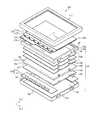
図4は、本発明の一実施形態に係るバックライトアセンブリを含む液晶表示装置200を概略的に示す分解斜視図である。本実施形態に係る液晶表示装置200は、バックライトアセンブリ191の構造を除いては、図1に示した液晶表示装置100と実質的に同一の構成要素を含む。つまり、本実施形態に係る液晶表示装置200は、液晶パネルアセンブリ120及びバックライトアセンブリ191を含む。 FIG. 4 is an exploded perspective view schematically showing a liquid
液晶パネルアセンブリ120は、液晶表示パネル123、チップフィルムパッケージ126、及びソース印刷回路基板128などを含む。 The liquid
液晶表示パネル123は、下部表示板122、下部表示板122に対向する上部表示板124と、両表示板122、124の間に介在された液晶層(図示せず)を含む。液晶表示パネル123は、バックライトアセンブリ191の上部に配置されて、バックライトアセンブリ191から供給される光を利用して画像情報を表示する。 The liquid
チップフィルムパッケージ126は、下部表示板122に形成された各データライン(図示せず)に接続されて、データ駆動信号を供給してもよい。ゲート駆動部は、下部表示板122に形成された各ゲートライン(図示せず)に接続されて、ゲート駆動信号を供給してもよい。一例によると、ゲート駆動部は、集積回路(integrated circuit)で形成してもよい。他の例によると、ゲート駆動部は、チップフィルムパッケージ126で形成してもよい。一方、ソース印刷回路基板127には、ゲート駆動部に入力されるゲート駆動部と、チップフィルムパッケージ126に入力されるデータ駆動信号を処理する幾つかの駆動部品を実装させてもよい。 The
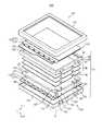
バックライトアセンブリ191は、光学シート140、モールドフレーム130、導光板150、反射板160、第1光源モジュール170a及び第2光源モジュール170b(図5参照)、並びに下部収納容器180などを含む。光学シート140、反射板160、モールドフレーム130については後述する。 The
図5は、第1及び第2光源モジュールと導光板(図1参照)の結合関係を示す斜視図である。 FIG. 5 is a perspective view showing the coupling relationship between the first and second light source modules and the light guide plate (see FIG. 1).
図4及び図5を参照すると、第1方向DI1に導光板150の一側及び一側と対向する他側にそれぞれ第1光源モジュール170a及び第2光源モジュール170bが配置されている。このような光源配置構造において、表示画面全体に均一に光が出射するようにするために導光板150は、厚さが実質的に均一なフラット(flat)タイプで形成してもよい。ただし、本発明の一実施形態では、これに限定されず、多様な形状の導光板150に適用してもよい。 4 and 5, the first
導光板150の構造は、説明の便宜上、第1光源モジュール170aを基準に入光面151、対向面152、出光面153、及び反射面154を含む。以下では、上記図1で導光板150の構成についての説明をしたため重複する説明は省略する。また、導光板150は、入光面151と対向面152を互いに接続する第1側面155及び第2側面156を含む。第1光源モジュール170aを基準にした入光面151及び対向面152は、それぞれ導光板150の他側に配置される第2光源モジュール170bの対向面及び入光面に該当する。 The structure of the
一方、導光板150の反射面154及び出光面153のうち、少なくとも一面には導光板150の内部の光が導光板150の上部に位置する液晶表示パネル123に放出されるように複数の拡散パターン(図示せず)を形成してもよい。導光板150から出射される光の輝度を一定に維持するために、導光板150の一面に形成された拡散パターンは、第1光源モジュール170a及び第2光源モジュール170bからの距離に応じて大きさと密度が異なるように形成してもよい。例えば、第1光源モジュール170a及び第2光源モジュール170bから遠くなるほど拡散パターンの密度を高くするか、または、拡散パターンの大きさを大きくすることによって、出光面153から出射される光の輝度を均一にすることが好ましい。このような拡散パターンは、インクをシルクスクリーン(silk screen)印刷するか、またはレーザ加工により形成してもよいが、本発明の一実施形態はこれに限定されない。例えば、導光板150に微細な溝または突起を形成して実質的に同一な作用効果を有する拡散パターンをシルクスクリーン印刷またはレーザ加工により形成してもよい。 On the other hand, at least one of the reflecting
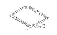
図5の第1光源モジュール170a及び第2光源モジュール170bは、導光板150の一側面に光を照射する複数の発光ダイオード171とそれぞれの発光ダイオード171に電気的に接続して駆動電源を印加する回路パターンが形成された発光ダイオード171駆動用印刷回路基板172(Printed Circuit Board:PCB)を含む。 The first
発光ダイオード171駆動用印刷回路基板172は、ベース基板を含み、ベース基板上に複数の発光ダイオード171に駆動電流を供給するためのパターニングされた伝導性物質からなる回路パターン及び回路パターンとの間の電気的短絡を防ぐ絶縁層(図示せず)からなる。ベース基板は、厚さ及び軟性に応じて硬性プレートまたは軟性フィルムから構成してもよい。また、ベース基板は、発光ダイオード171から発生した熱を効率よく放出するための金属板(図示せず)によって支持してもよい。このとき、金属板は、光源モジュール170の機械的安定性を図ってもよい。 The printed
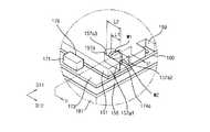
本実施形態では、それぞれの光源モジュール170の入光距離を一定に維持するための光源モジュール170の印刷回路基板172の上面173に突起174が形成される。図5に示すように、第1光源モジュール170aの印刷回路基板172が第1方向DI1の短辺と第2方向DI2の長辺を有する平面とするとき、突起174は、第1光源モジュール170aの印刷回路基板172の両側短辺と隣接する部位に形成してもよい。 In the present embodiment, a
例えば、突起174は、光源モジュール170の発光ダイオード171から導光板150に向かって配置してもよい。また、突起174は光源モジュール170の最外郭に配置された発光ダイオード171より外側に配置してもよい。また、第2光源モジュール170bの印刷回路基板172においても第1光源モジュール170aの印刷回路基板172の突起174と第2方向DI2を基準にして対称的に突起174を形成してもよい。 For example, the
突起174は、表面実装法によってはんだ付け工程で印刷回路基板172に形成してもよい。この場合、突起174の材質は、はんだ付けが可能な金属性材質を含む。突起174の他の形成方法としては、突起174が形成される部分に印刷回路基板172に貫通ホール(図示せず)を形成し、貫通ホールと結合される部材を有する突起174を形成する。この場合、突起174は、樹脂性材質を含んでもよい。 The
印刷回路基板172上に形成される突起174は、導光板150の光学特性に影響を与えない程度でその数を決めてもよい。例えば、突起174は、印刷回路基板172の両側端部にそれぞれ1つずつ形成してもよい。本発明の一実施形態に係る突起174は、シリンダー状に配置される。また、突起174の形状は、長方形体、六角柱状などの多様な形態に変形してもよい。 The number of the
本実施形態に係る印刷回路基板172には、発光ダイオード171から発生される熱を放出するために印刷回路基板172の背面に銅(Cu)、アルミニウム(Al)等とともに熱伝導性金属材質の放熱板(図示せず)を形成してもよく、放熱の流れを円滑にするための放熱パターン(図示せず)を形成してもよい。さらに、印刷回路基板172の背面に非接着特性を有する熱伝導性テープを付着するか、または放熱グリース(thermal grease)を塗布して後述する印刷回路基板172の背面の流動性を確保してもよい。 In the printed
以下、図4及び図5を再び参照して光源モジュール170の入光距離を一定に維持するために突起174と対応する位置で突起174と結合する固定溝157について説明する。 Hereinafter, the fixing
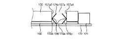
図5を参照すると、固定溝157(固定溝157a、157b、157c、157dに相当)は、導光板150の入光面151と対向面152を接続する側面155、156の端部に形成される。この場合、固定溝157は、第1側面の一側端部に形成される。固定溝157は、第1側面の両側端部に形成してもよい。つまり、固定溝157は、入光面151と第1側面または対向面152と第1側面とが互いに合う接線で所定間隔離隔された位置に形成してもよい。 Referring to FIG. 5, the fixing grooves 157 (corresponding to the fixing
固定溝157が形成される位置は、光源モジュール170の入光効率が最大になる入光距離に対応する。入光面151及び対向面152の近くに形成された固定溝157をそれぞれ第1固定溝157a及び第2固定溝157bとする場合、第1固定溝157aと第2固定溝157bは導光板150を第2方向DI2と平行に中心を横切る仮想線を基準に対称になるように配置してもよい。 The position where the fixing
一方、光源モジュール170が導光板150の両側に全て形成される場合、第1光源モジュール170aを基準に、上記したように第1固定溝157a及び第3固定溝157cが形成され、第2光源モジュール170bを基準に第2固定溝157b及び第4固定溝157dが形成されてもよい。図6は、図4の「A」部分を拡大した拡大斜視図であり、図7は、図6のII−II’線に沿って切断した断面図である。 On the other hand, when all the
図4において、第1固定溝157aと対応する第1光源モジュール170aの突起174を第1突起174aとする。先ず、第1突起174aに対応する第1固定溝157aは、第1方向DI1の幅W2と第2方向DI2の長さL2を有し、この場合、長さL2が幅W2より長い。 In FIG. 4, the
導光板150は、周囲環境によって第1及び第2方向に伸縮する。導光板150が第1方向DI1に伸縮する場合、導光板150は、第1突起174aと結合及び固定され、導光板150がPCB172に付着され、導光板150の伸縮とともにPCB172が流動して入光距離を維持する。導光板150が第2方向に伸縮する場合、導光板150は、自由自在に流動することによって、導光板150の撓み及び収縮を防止してもよい。従って、導光板150は、第2方向DI2の伸縮に流動性を確保するための長さL2が幅W2より大きいことが望ましい。 The
バックライトアセンブリ190で第1突起174aと第1固定溝157aのそれぞれの幅が実質的に同一で互いに接触するように結合されるか、または、第1突起174aの幅W1が第1固定溝157aの幅W2よりも少し小さく設定してもよい。周囲温度及び湿度などによって導光板150が第1方向DI1に伸縮する場合、第1突起174aと第1固定溝157aの接着によって複数の発光ダイオード171を含む印刷回路基板172または導光板150の伸縮率と実質的に同一な程度に移動されることによって、入光距離を一定に維持してもよい。 In the backlight assembly 190, the
印刷回路基板172が下部収納容器180の底板181と固定されていない流動構造を有することによって導光板150の入光面151と発光ダイオード171の上面178の離隔距離、つまり、入光距離を実質的に均一に維持してもよい。即ち、印刷回路基板172の下面は、下部収納容器180の底板181に対して独立的に流動する反面、導光板150には連動して流動するため、導光板150の入光面151と発光ダイオード171の上面178との間の距離が温度または湿度の変化にも誤差範囲内で一定に維持することによって、導光板の出光面においての輝度は均一または強度を維持してもよい。 Since the printed
さらに、突起174と固定溝157の幅は、組立誤差を含んで最適な関係に設定することが可能であり、望ましくは、導光板150に沿って形成される固定溝157の幅は、突起174の幅より大きく形成される。ここで、固定溝と突起それぞれの幅は、印刷回路基板172の伸縮率を共に考慮して算定してもよい。 Furthermore, the width of the
本発明の一実施形態に係る第1固定溝157aは、図6に示すように第1側面155で導光板150の内部に向かって延長される。第1固定溝157aは、互いに向い合う第1内側面157a1と第2内側面157a2を含み、それぞれの内側面を繋ぐ接続面157a3を有してもよい。 The
このような構造の固定溝157は、導光板150の側面から隣接した所に突起174が貫通するように突起貫通用ホールを設けて形成できる。また、図4,5及び6に示すように、固定溝157は、貫通ホールを形成することより組立の容易性に優れるように溝の形状で形成してもよい。接続面157a3は、第1突起174aの外面のうち、一部が接触するようにラウンド形状の曲面で形成してもよく、本実施形態の場合、接触面157a3は、円柱の第1突起174aと対応するようにアーチ状の曲面を有する。本発明の実施形態の接続面は、多様な形態の平面または曲面を有してもよく、本発明の実施形態に限定するのではない。 The fixing
第1突起174aは、第1固定溝157aに対応する位置に形成してもよい。つまり、第1突起174aは発光ダイオード171の放射角を考慮して最外郭に位置した発光ダイオード171の放射角領域の外、つまり、デッドゾーン(dead zone)に位置してもよい。一方、PCBの幅は狭ければ狭いほどよく、この場合、第1突起174aが最大限の入光面151の第1方向DI1に位置してもよい。また、第1突起174a付近の第1固定溝157a周辺のパターンは、光が全面に広がるようにパターンの密度を高めてもよい。この場合、第1突起174aと第1固定溝157aは上部に配置されたモールドフレーム130によってカバーされるため、実質的に表示品質には影響を与えない。 The
図7は、図6のII−II’線に沿って切断した断面図であり、上述したように第1突起174aと第1固定溝157aの結合関係を示す。 FIG. 7 is a cross-sectional view taken along the line II-II ′ of FIG. 6, and shows the coupling relationship between the
図8は、本発明の他の実施形態に係るバックライトアセンブリを示す断面図である。 FIG. 8 is a cross-sectional view illustrating a backlight assembly according to another embodiment of the present invention.
本実施形態に係るバックライトアセンブリは、突起174と固定溝157の接着構造を除いては図6及び図7のバックライトアセンブリと同一であるため、重複する説明は省略する。 The backlight assembly according to the present embodiment is the same as the backlight assembly of FIGS. 6 and 7 except for the bonding structure of the
本実施形態に係る第1突起174aは、突起本体の外面にスプリングなどのような弾性部材174−1が配置された形態であってもよい。弾性部材174−1の一端は、第1固定溝157aの幅方向の内側面157a1、157a2と当接されていて、導光板150の第1固定溝157a形成のときに発生する加工誤差を減少してもよい。この場合、第1突起174aと第1固定溝157aを所定の弾性を有するように相互密着させて光源モジュール170の入光距離の維持に寄与してもよい。また、弾性部材174−1を適用することによって、印刷回路基板の伸縮にも関わらず、印刷回路基板と導光板の位置が同一な変位を有することによって入光距離の維持をさらに容易にしてもよい。 The
図9は、本発明のまた他の実施形態に係るバックライトアセンブリを示す断面図である。 FIG. 9 is a cross-sectional view illustrating a backlight assembly according to still another embodiment of the present invention.
本実施形態に係るバックライトアセンブリは、突起174と固定溝157の接着構造を除いて図6及び図7のバックライトアセンブリと同一であるため、重複する説明は省略する。 The backlight assembly according to the present embodiment is the same as the backlight assembly of FIGS. 6 and 7 except for the bonding structure of the
本実施形態に係る第1突起174aは、互いに対向する一対の突出部を有する板状弾性部材を含む。板状弾性部材は、印刷回路基板172の上面に形成された基底部175a、基底部175aから突出された第1の突出部175bと、基底部175から突出されて第1固定溝157aの内側面157a1、157a2にそれぞれ延長される第1突出部175b及び第2突出部175cを含み、第1突出部175b及び第2突出部175cはそれぞれ内側面157a1、175a2と接触する折曲部176を有する。ただし、板状弾性部材は、図9の形態に限定されず、多様な形態で変形してもよい。板状弾性部材の折曲部176は、第1固定溝157の内側面157a1、157a2と互いに当接する構造からなり、固定溝157の加工誤差、または、外部からの衝撃によって第1突起174aと第1固定溝157aが接触されずに隙間の発生を防いでもよい。 The
図10及び図11は、本発明のまた他の実施形態に係るバックライトアセンブリを示す斜視図である。 10 and 11 are perspective views illustrating a backlight assembly according to still another embodiment of the present invention.
図10及び図11は光源モジュール170と導光板150の結合関係を除いては図4のバックライトアセンブリと同一であるため、重複する説明は省略する。 10 and 11 are the same as the backlight assembly of FIG. 4 except for the coupling relationship between the
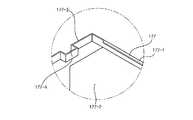
図10のバックライトアセンブリは、複数の発光ダイオード171と印刷回路基板172を含む光源モジュール170の背面に光源モジュールカバー177をさらに含む。 The backlight assembly of FIG. 10 further includes a light
光源モジュール170と光源モジュールカバー177は接着性テープまたはネジなどで固定されて一体で形成される。光源モジュールカバー177は、発光ダイオードから放出される熱を吸収して外部に伝達を容易にする金属プレートであってもよい。その上面に銀(Ag)のような反射性物質がコーティングされて、発光ダイオードから放出される白色光を導光板150の入光面151に向かって入射できるように反射するため反射効率が向上する。 The
本実施形態に係る印刷回路基板172は、本発明の他の実施形態と異なる複数の発光ダイオード171が配置される一面が導光板150の入光面151と対向して平行に整列される。 In the printed
図11は、光源モジュールカバー177の構造を示す図である。光源モジュールは、印刷回路基板172が配置されて複数の発光ダイオードを固定する支持部177−1、支持部177-1の縁から延長されて導光板150の反射面154と一部オーバーラップされる底板177−2及び支持部177−1の一段から導光板150の第1側壁155に沿って延長されて形成される締結部177−3から構成される。 FIG. 11 is a view showing the structure of the light
図10に示すように、締結部177−3は、導光板150の締結溝158の内面158−1に沿って延長される導光板の固定部177−4を含む。光源モジュールカバー177の締結部177−3と導光板150の締結溝158の結合によって上記した光源モジュール170の入光距離を一定に維持させる機能を有することになる。締結部177−3と締結溝158は本実施形態に限定されることではなく、多様に変形してもよい。 As shown in FIG. 10, the fastening portion 177-3 includes a light guide plate fixing portion 177-4 that extends along the inner surface 158-1 of the
図12は、本発明のさらに他の実施形態に係るバックライトアセンブリ示す斜視図である。 FIG. 12 is a perspective view showing a backlight assembly according to still another embodiment of the present invention.
図12を参照すると、本実施形態に係るバックライトアセンブリは印刷回路基板172が金属支持体179をさらに含むことを除いては図4のバックライトアセンブリと実質的に同一であるため重複する説明は省略する。 Referring to FIG. 12, the backlight assembly according to the present embodiment is substantially the same as the backlight assembly of FIG. 4 except that the printed
本実施形態に係るバックライトアセンブリの印刷回路基板172は、金属支持体179をさらに含む。金属支持体179は、導光板の反射面154とオーバーラップされる水平部179a及び水平部179aで曲げられて延長し、導光板の第1側面155及び第2側面156とオーバーラップされる垂直部179bを含む。この場合、金属支持体179の水平部179aの角部分には突起174が形成されて導光板の固定溝157と互いに結合してもよい。突起174の形状及び形成位置は、上記において説明したことと同一であるため省略する。このように、金属支持体179に突起174が形成され、垂直部及び水平部が導光板150をカバーすることによって、導光板150をより安定的に固定してもよい。 The printed
図13は、図4のモールドフレーム示す平面図である。 FIG. 13 is a plan view showing the mold frame of FIG.
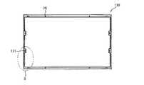
図14は、図13の「B」部分を拡大した拡大斜視図である。 FIG. 14 is an enlarged perspective view in which the “B” portion of FIG. 13 is enlarged.
以下、図4、図13、図14を参照して、バックライトアセンブリ190の反射板160、光学シート140及び下部収納容器180について説明する。 Hereinafter, the
先ず、反射板160は、導光板150の反射面154と下部収納容器180の底板181との間に位置して、導光板150の反射面154から放出される光を上部に反射する。反射板160には突起174が形成された位置と対応する一部分に、貫通ホール161(図4参照)が形成される。貫通ホール161と通じて突起174が挿入及び固定されて、組立を容易にしている。光学シート140は、バックライトアセンブリ191と液晶パネルアセンブリ120との間に配置されて、光効率を増加させる。光学シート140はそれぞれ光学シート本体141、光学シートの縁に形成された光学シートガイド溝142から構成してもよい。光学シートガイド溝142はモールドフレーム130(後述する)のガイド突出部が結合されて光学シート本体を固定し、流動を防ぐ役割をする。このように光学シート140の構成は、上述の実施形態に限定されず、表示装置の仕様に応じて多様に変形してもよい。下部収納容器180は四角形状を有する底板181及び底板181のエッジから延長されて収納空間を形成する側壁を含んでよい。側壁は、第1方向DI1に互いに平行に対向して配置される第1側壁182及び第2側壁183、第2方向DI2に互いに平行に対向して配置される第3側壁184及び第4側壁185からなる。通常、下部収納容器180の収納空間には発光ダイオード171用印刷回路基板172、反射板160、導光板150、光学シート140が順に収納される。 First, the
図13において、モールドフレーム130は、四角枠状の側部133と、側部133から内側に延長された第1指示部134(図14参照)及び第2支持部135(図14参照)を含む。第1支持部134の一面には液晶表示パネルを配置し、他面には光学シート140及び導光板150が順に配置される。第2支持部135は、第1支持部134の他面上に形成されて光学シート140及び導光板150の流動を防ぎ、第2支持部135の厚さは、光学シート140及び導光板150の厚さの和と実質的に同一であってもよい。モールドフレーム130の内側に向かって第2支持部135から突出されたガイド突出部136は、光学シート140及び導光板150の動きを制御する。例えば、光学シート140の縁に形成されたガイド溝142と導光板150の縁に形成されたガイド溝159にモールドフレーム130のガイド突出部136が挿入される。 In FIG. 13, the
第2支持部135には反射板160が配置され、反射板160を固定するための第2支持部135の一面に固定ピン131を形成してもよい。本発明の一実施形態においては、固定ピン131が第2支持部135のガイド突出部136上に形成されている場合を例として説明しているが、本発明はこれに限定されず、第2支持部135上の任意の位置に配置してもよい。例えば、固定ピン131は、反射板160の挿入ホール162に挿入される。第1支持部134または第2支持部135上には反射板160と対向するように突出された追加固定ピン20を形成してもよく、この場合、追加固定ピン20は、反射板160を上から押して下部収納容器180の底板181に固定させる役割をする。 A
モールドフレーム130の角部には側部133と実質的に平行に第2支持部135から突出された固定突出部137が形成されている。固定突出部137と側部133との間には「U」字状の挿入空間が設けられ、その挿入空間に下部収納容器180の第3側壁184及び第4側壁185を挿入して固定される。本発明の一実施形態においては下部収納容器180とモールドフレーム130が結合して光学シート140、導光板150、及び反射板160を収納する構造を有しているが、下部収納容器180の第1側壁182及び第2側壁183は、モールドフレーム130の外側でモールドフレーム130とフック方式で結合され、下部収納容器180の第3側壁184及び第4側壁185はモールド130の内側に設けられた挿入空間に挿入し固定されるため、モールドフレーム130と下部収納容器180間の結合力を充分に確保してもよい。 A fixed protruding
以上、添付図面を参照しながら本発明の好適な実施形態について詳細に説明したが、本発明は係る実施形態に限定されない。本発明の属する技術分野における通常の知識を有する者であれば、特許請求の範囲に記載された技術的思想の範囲内において、各種の変形例または修正例に想到し得ることは明らかであり、これらについても、当然に本発明の技術的範囲に属するものと理解される。 The preferred embodiments of the present invention have been described in detail above with reference to the accompanying drawings, but the present invention is not limited to such embodiments. It is obvious that a person having ordinary knowledge in the technical field to which the present invention belongs can come up with various modifications or modifications within the scope of the technical idea described in the claims. Of course, these are also understood to belong to the technical scope of the present invention.
100 液晶表示装置
110 トップシャーシ
130 モールドフレーム
131 固定ピン
132 フック
133 側部
134 第1支持部
135 第2支持部
136 ガイド突出部
137 固定突出部
142、159 ガイド溝
150 導光板
157 固定溝
158 締結溝
170a、170b 光源モジュール
174 突起
177 光源モジュールカバー
180 下部収納容器
181 底板
190 バックライトアセンブリDESCRIPTION OF
Claims (10)
Translated fromJapanese光が入射される入光面、前記入光面の縁から延長し形成された側面、前記側面から導光板の内部光源に向かって形成された固定溝を有する導光板と、
前記点光源が配置された点光源配置部、前記点光源配置部から前記第1方向と実質的に垂直する第2方向に延長し形成された延長部、及び前記延長部の縁に固定される突起を有する印刷回路基板と、を含み、
前記固定溝は、前記第2方向の幅と前記第1方向の長さを有し、前記長さが前記幅より大きく、
前記印刷回路基板の前記突起は前記導光板の前記固定溝と結合され、
前記導光板の伸縮とともに前記印刷回路基板が流動することを特徴とするバックライトアセンブリ。A plurality of point light sources emitting light and arranged in a first direction;
A light incident plate on which light is incident, a side surface formed extending from an edge of the light incident surface, a light guide plate having a fixing groove formed from the side surface toward an internal light source of the light guide plate;
A point light source arrangement part in which the point light source is arranged, an extension part extending from the point light source arrangement part in a second direction substantially perpendicular to the first direction, and an edge of the extension part A printed circuit board having a protrusion, and
The fixing groove has a width in the second direction and a length in the first direction, and the length is larger than the width.
The protrusion of the printed circuit board is coupled to the fixing groove of the light guide plate;
The backlight assembly, wherein the printed circuit board flows as the light guide plate expands and contracts .
The backlight assembly of claim 1, wherein a height of the protrusion is smaller than or substantially equal to a thickness of the light guide plate.
Applications Claiming Priority (2)
| Application Number | Priority Date | Filing Date | Title |
|---|---|---|---|
| KR1020090116409AKR101698816B1 (en) | 2009-11-30 | 2009-11-30 | Backlight assembly |
| KR10-2009-0116409 | 2009-11-30 |
Publications (2)
| Publication Number | Publication Date |
|---|---|
| JP2011119218A JP2011119218A (en) | 2011-06-16 |
| JP5778899B2true JP5778899B2 (en) | 2015-09-16 |
Family
ID=42355366
Family Applications (1)
| Application Number | Title | Priority Date | Filing Date |
|---|---|---|---|
| JP2010162578AActiveJP5778899B2 (en) | 2009-11-30 | 2010-07-20 | Backlight assembly |
Country Status (6)
| Country | Link |
|---|---|
| US (4) | US8297823B2 (en) |
| EP (2) | EP2362263B1 (en) |
| JP (1) | JP5778899B2 (en) |
| KR (1) | KR101698816B1 (en) |
| CN (1) | CN102080785B (en) |
| TW (1) | TWI499839B (en) |
Families Citing this family (51)
| Publication number | Priority date | Publication date | Assignee | Title |
|---|---|---|---|---|
| KR20100127177A (en)* | 2009-05-25 | 2010-12-03 | 삼성전자주식회사 | Display device backlight |
| KR101698816B1 (en)* | 2009-11-30 | 2017-01-24 | 삼성디스플레이 주식회사 | Backlight assembly |
| WO2011122060A1 (en)* | 2010-03-31 | 2011-10-06 | シャープ株式会社 | Illumination apparatus and display device |
| EP2431654B1 (en)* | 2010-09-17 | 2018-11-14 | LG Innotek Co., Ltd. | Lighting module and lighting apparatus including the same |
| JP2012109207A (en)* | 2010-10-18 | 2012-06-07 | Meitaku Kogyo Kk | Surface lighting body |
| WO2012073817A1 (en)* | 2010-12-03 | 2012-06-07 | シャープ株式会社 | Illumination device, display device and television receiving device |
| TWI416034B (en)* | 2011-05-02 | 2013-11-21 | Advanced Optoelectronic Tech | Structure of the flat type lighting |
| JP2012243541A (en)* | 2011-05-19 | 2012-12-10 | Sanyo Electric Co Ltd | Light emitting device and liquid crystal display device |
| JP5747712B2 (en) | 2011-07-25 | 2015-07-15 | セイコーエプソン株式会社 | LIGHTING DEVICE, LIQUID CRYSTAL DISPLAY DEVICE, AND ELECTRONIC DEVICE |
| US20130027971A1 (en)* | 2011-07-29 | 2013-01-31 | Enlight Corporation | Dazzle prevention lighting fixture with light guide means to disperse emitted light uniformly |
| KR101288600B1 (en) | 2011-09-15 | 2013-07-22 | 엘지디스플레이 주식회사 | Back light unit for liquid crystal display device |
| CN102322600A (en)* | 2011-10-12 | 2012-01-18 | 深圳市华星光电技术有限公司 | A kind of module backlight and liquid crystal indicator |
| CN102661528B (en)* | 2012-04-05 | 2014-05-21 | 深圳市华星光电技术有限公司 | Backlight module and LCD (liquid crystal display) |
| KR20130116704A (en)* | 2012-04-16 | 2013-10-24 | 삼성디스플레이 주식회사 | Backlight assembly and display apparatus having the same |
| EA027711B1 (en)* | 2012-05-23 | 2017-08-31 | Агк Гласс Юроп | Led illuminated glass insulating panel |
| US10036848B2 (en)* | 2012-08-28 | 2018-07-31 | Sharp Kabushiki Kaisha | Lighting device, display device, and television device |
| TWI472851B (en)* | 2012-10-09 | 2015-02-11 | Au Optronics Corp | Display, backlight module, and frame structure thereof |
| KR102096400B1 (en)* | 2012-10-17 | 2020-04-06 | 삼성전자주식회사 | Liquid Crystal Display |
| US8926163B2 (en)* | 2012-10-24 | 2015-01-06 | Shenzhen China Star Optoelectronics Technology Co., Ltd | Liquid crystal display and the backlight module thereof |
| CN102927499B (en) | 2012-10-24 | 2015-02-11 | 深圳市华星光电技术有限公司 | Liquid crystal display device and backlight module thereof |
| US20140119055A1 (en)* | 2012-10-31 | 2014-05-01 | Shenzhen China Star Optoelectronics Technology Co., Ltd. | Light Coupling Arrangement of Backlight Module |
| KR101418920B1 (en)* | 2012-12-26 | 2014-07-11 | 엘지디스플레이 주식회사 | Backlight unit for liquid crystal display device |
| WO2014109301A1 (en)* | 2013-01-09 | 2014-07-17 | シャープ株式会社 | Illumination device, display device and tv receiver |
| JP2014153370A (en) | 2013-02-04 | 2014-08-25 | Panasonic Liquid Crystal Display Co Ltd | Display device |
| CN103162246B (en)* | 2013-03-08 | 2014-06-11 | 西蒙电气(中国)有限公司 | Light-emitting diode (LED) panel light assembly system |
| KR101658396B1 (en)* | 2013-03-21 | 2016-09-21 | 엘지디스플레이 주식회사 | Display device |
| CN103307486B (en)* | 2013-06-19 | 2015-10-28 | 苏州信亚科技有限公司 | A kind of LED fluorescent lamp tube |
| WO2014207936A1 (en)* | 2013-06-28 | 2014-12-31 | 堺ディスプレイプロダクト株式会社 | Light-source device and display device |
| JP6199971B2 (en)* | 2013-07-18 | 2017-09-20 | 堺ディスプレイプロダクト株式会社 | Light source device and display device |
| CN103454801B (en)* | 2013-09-09 | 2016-05-04 | 深圳市华星光电技术有限公司 | Backlight framework and backlight module |
| CN104597553B (en)* | 2013-10-30 | 2017-09-12 | 纬创资通股份有限公司 | Light guide plate |
| CN105705986B (en)* | 2013-11-08 | 2019-05-10 | 堺显示器制品株式会社 | Display device |
| US9952381B2 (en)* | 2014-01-06 | 2018-04-24 | Sakai Display Products Corporation | Light source device and display apparatus |
| WO2015178302A1 (en)* | 2014-05-23 | 2015-11-26 | シャープ株式会社 | Illumination device and display device |
| TWI544173B (en)* | 2014-06-17 | 2016-08-01 | 緯創資通股份有限公司 | Black light module with mount and displaying apparatus therewith |
| JP2016029470A (en)* | 2014-07-24 | 2016-03-03 | 船井電機株式会社 | Display device |
| KR102272319B1 (en) | 2014-12-05 | 2021-07-05 | 삼성디스플레이 주식회사 | Curved display |
| CN104570478B (en)* | 2014-12-30 | 2017-05-03 | 深圳市华星光电技术有限公司 | Liquid-crystal display device and manufacturing method of light guide plate positioning block |
| CN104678613B (en)* | 2015-02-13 | 2018-07-06 | 深超光电(深圳)有限公司 | Liquid crystal display device |
| CN105240714A (en)* | 2015-09-21 | 2016-01-13 | 京东方科技集团股份有限公司 | Light emitting diode light bar, back light source and display device |
| CN105179981A (en)* | 2015-10-19 | 2015-12-23 | 合肥京东方显示光源有限公司 | Light guide plate, backboard, lateral backlight module and display device |
| KR102519862B1 (en)* | 2015-12-24 | 2023-04-10 | 엘지디스플레이 주식회사 | Optical sheet and display apparatus having the same |
| KR102504803B1 (en)* | 2016-04-06 | 2023-02-28 | 엘지전자 주식회사 | Display device |
| GB2552807B (en)* | 2016-08-10 | 2019-03-20 | Lightly Tech Limited | A planar LED light source module |
| KR20180065734A (en)* | 2016-12-08 | 2018-06-18 | 삼성전자주식회사 | Packing materials for display apparatus and packing method for display apparatus |
| CN206479671U (en)* | 2017-03-01 | 2017-09-08 | 合肥京东方光电科技有限公司 | A kind of light guide plate, backlight and display device |
| CN110335569B (en)* | 2019-07-11 | 2021-01-26 | 京东方科技集团股份有限公司 | Edge light type backlight module and driving method thereof, and display device |
| FR3104679B1 (en)* | 2019-12-13 | 2022-07-15 | Valeo Vision | Optical part and light module for motor vehicle |
| CN113568219B (en)* | 2020-04-28 | 2023-03-28 | 华为技术有限公司 | Backlight and display device |
| CN111897042B (en)* | 2020-07-23 | 2022-11-04 | 苏州伊尔顿光电科技有限公司 | Novel light guide plate |
| CN114530097A (en)* | 2022-03-15 | 2022-05-24 | Tcl华星光电技术有限公司 | Display device |
Family Cites Families (29)
| Publication number | Priority date | Publication date | Assignee | Title |
|---|---|---|---|---|
| KR100238004B1 (en)* | 1997-08-30 | 2000-01-15 | 구본준 | Fixing structure of light distribution device of liquid crystal display device |
| JP3998810B2 (en) | 1998-05-28 | 2007-10-31 | 三菱電機株式会社 | LIGHTING DEVICE AND LIQUID CRYSTAL DISPLAY DEVICE USING THE SAME |
| JP2002196312A (en)* | 2000-12-25 | 2002-07-12 | Hitachi Ltd | Liquid crystal display |
| JP2004184493A (en)* | 2002-11-29 | 2004-07-02 | Seiko Epson Corp | Electro-optical device, method of manufacturing electro-optical device, and electronic apparatus |
| KR20050015368A (en) | 2003-08-05 | 2005-02-21 | 엘지.필립스 엘시디 주식회사 | The back light unit for the liquid crystal display device |
| JP4543779B2 (en)* | 2004-06-25 | 2010-09-15 | 日亜化学工業株式会社 | Semiconductor light emitting device |
| JP2006032020A (en)* | 2004-07-13 | 2006-02-02 | Sharp Corp | Liquid crystal display |
| TWI241142B (en)* | 2004-08-03 | 2005-10-01 | Jemitek Electronics Corp | Flat display module |
| US7515220B2 (en)* | 2005-04-01 | 2009-04-07 | Samsung Electronics Co., Ltd. | Display device |
| KR20070000855A (en) | 2005-06-28 | 2007-01-03 | 엘지.필립스 엘시디 주식회사 | LCD module with light leakage prevention means |
| JP4071788B2 (en)* | 2005-08-31 | 2008-04-02 | 株式会社東芝 | Apparatus and method for removing cross color and dot interference |
| CN1924664A (en) | 2005-09-02 | 2007-03-07 | 群康科技(深圳)有限公司 | Back light module unit |
| KR20070048516A (en) | 2005-11-04 | 2007-05-09 | 삼성전자주식회사 | Back light assembly and liquid crystal display device having same |
| KR101224376B1 (en) | 2006-01-25 | 2013-01-21 | 삼성디스플레이 주식회사 | Backlight assembly and liquid crystal display apparatus having the same |
| KR20070097676A (en) | 2006-03-28 | 2007-10-05 | 삼성전자주식회사 | Display device |
| KR20070101517A (en) | 2006-04-11 | 2007-10-17 | 희성전자 주식회사 | Side type backlight unit using light emitting diode as light source |
| KR20080004006A (en) | 2006-07-04 | 2008-01-09 | 삼성전자주식회사 | Backlight unit and liquid crystal display having the same |
| JP4706858B2 (en)* | 2006-07-10 | 2011-06-22 | ミネベア株式会社 | Surface lighting device |
| JP2008243402A (en)* | 2007-03-26 | 2008-10-09 | Mitsubishi Electric Corp | Planar light source device, method of assembling the same, and display device using the same |
| KR100824866B1 (en)* | 2007-05-28 | 2008-04-23 | 삼성에스디아이 주식회사 | Liquid crystal display |
| KR101277852B1 (en) | 2007-07-27 | 2013-06-21 | 엘지디스플레이 주식회사 | Backlight unit and liquid crystal display device having the same |
| KR20090022177A (en)* | 2007-08-29 | 2009-03-04 | 엘지디스플레이 주식회사 | LCD Display |
| JP5074135B2 (en)* | 2007-09-18 | 2012-11-14 | 株式会社ジャパンディスプレイイースト | Liquid crystal display |
| JP4909866B2 (en)* | 2007-10-10 | 2012-04-04 | 富士フイルム株式会社 | Surface lighting device |
| JP5414224B2 (en)* | 2007-10-19 | 2014-02-12 | 富士フイルム株式会社 | Surface lighting device |
| KR20090048862A (en)* | 2007-11-12 | 2009-05-15 | 엘지디스플레이 주식회사 | Liquid crystal display |
| JP2010113904A (en)* | 2008-11-05 | 2010-05-20 | Fujikura Ltd | Planar light emitting device, electronic equipment, and manufacturing method of planar light emitting device |
| KR20100127177A (en)* | 2009-05-25 | 2010-12-03 | 삼성전자주식회사 | Display device backlight |
| KR101698816B1 (en)* | 2009-11-30 | 2017-01-24 | 삼성디스플레이 주식회사 | Backlight assembly |
- 2009
- 2009-11-30KRKR1020090116409Apatent/KR101698816B1/enactiveActive
- 2010
- 2010-05-20USUS12/784,361patent/US8297823B2/enactiveActive
- 2010-06-04TWTW099118273Apatent/TWI499839B/enactive
- 2010-06-16EPEP10006226.4Apatent/EP2362263B1/enactiveActive
- 2010-06-16EPEP18175670.1Apatent/EP3388890B1/enactiveActive
- 2010-07-20JPJP2010162578Apatent/JP5778899B2/enactiveActive
- 2010-09-09CNCN201010279221.9Apatent/CN102080785B/enactiveActive
- 2012
- 2012-10-29USUS13/663,307patent/US8636399B2/enactiveActive
- 2014
- 2014-01-02USUS14/146,254patent/US8840293B2/enactiveActive
- 2014-08-13USUS14/458,995patent/US9529135B2/enactiveActive
Also Published As
| Publication number | Publication date |
|---|---|
| EP3388890A1 (en) | 2018-10-17 |
| EP3388890B1 (en) | 2020-05-13 |
| TWI499839B (en) | 2015-09-11 |
| US9529135B2 (en) | 2016-12-27 |
| EP2362263A1 (en) | 2011-08-31 |
| CN102080785B (en) | 2016-06-22 |
| US8636399B2 (en) | 2014-01-28 |
| EP2362263B1 (en) | 2018-09-05 |
| KR101698816B1 (en) | 2017-01-24 |
| US20110128756A1 (en) | 2011-06-02 |
| KR20110059955A (en) | 2011-06-08 |
| JP2011119218A (en) | 2011-06-16 |
| US8297823B2 (en) | 2012-10-30 |
| US20130051077A1 (en) | 2013-02-28 |
| US20140119054A1 (en) | 2014-05-01 |
| TW201207498A (en) | 2012-02-16 |
| CN102080785A (en) | 2011-06-01 |
| US8840293B2 (en) | 2014-09-23 |
| US20140347887A1 (en) | 2014-11-27 |
Similar Documents
| Publication | Publication Date | Title |
|---|---|---|
| JP5778899B2 (en) | Backlight assembly | |
| CN101737678B (en) | Backlight assembly, display device having same, and method of manufacturing display device | |
| CN102042539B (en) | Backlight assembly and display device having the same | |
| US7441938B2 (en) | Planar light source device | |
| US8434925B2 (en) | Light source device and surface light source device equipped with same | |
| CN101416101B (en) | Liquid crystal display | |
| TWI432846B (en) | Backlight unit and liquid crystal display having the same | |
| JP6412175B2 (en) | Backlight assembly and display device including backlight assembly | |
| CN101988648A (en) | Backlight unit and liquid crystal display using the same | |
| JP2004349143A (en) | Planar light source device and display device | |
| JP5293772B2 (en) | Planar light source device and display device | |
| JP5556856B2 (en) | Planar light source device and liquid crystal display device | |
| US10317611B2 (en) | Display device | |
| KR101283068B1 (en) | The radiant heat circuit board unified blanket and the backlight unit having the same | |
| KR102057990B1 (en) | The radiant heat circuit board unified blanket and the backlight unit having the same | |
| WO2014057990A1 (en) | Edge light-type surface light source device and liquid crystal display device | |
| KR102070639B1 (en) | The radiant heat circuit board and the backlight unit having the same |
Legal Events
| Date | Code | Title | Description |
|---|---|---|---|
| A711 | Notification of change in applicant | Free format text:JAPANESE INTERMEDIATE CODE: A712 Effective date:20121213 | |
| A621 | Written request for application examination | Free format text:JAPANESE INTERMEDIATE CODE: A621 Effective date:20130703 | |
| A977 | Report on retrieval | Free format text:JAPANESE INTERMEDIATE CODE: A971007 Effective date:20140418 | |
| A131 | Notification of reasons for refusal | Free format text:JAPANESE INTERMEDIATE CODE: A131 Effective date:20140507 | |
| A521 | Request for written amendment filed | Free format text:JAPANESE INTERMEDIATE CODE: A523 Effective date:20140807 | |
| A131 | Notification of reasons for refusal | Free format text:JAPANESE INTERMEDIATE CODE: A131 Effective date:20150106 | |
| A521 | Request for written amendment filed | Free format text:JAPANESE INTERMEDIATE CODE: A523 Effective date:20150402 | |
| TRDD | Decision of grant or rejection written | ||
| A01 | Written decision to grant a patent or to grant a registration (utility model) | Free format text:JAPANESE INTERMEDIATE CODE: A01 Effective date:20150616 | |
| A61 | First payment of annual fees (during grant procedure) | Free format text:JAPANESE INTERMEDIATE CODE: A61 Effective date:20150710 | |
| R150 | Certificate of patent or registration of utility model | Ref document number:5778899 Country of ref document:JP Free format text:JAPANESE INTERMEDIATE CODE: R150 | |
| R250 | Receipt of annual fees | Free format text:JAPANESE INTERMEDIATE CODE: R250 | |
| R250 | Receipt of annual fees | Free format text:JAPANESE INTERMEDIATE CODE: R250 | |
| R250 | Receipt of annual fees | Free format text:JAPANESE INTERMEDIATE CODE: R250 | |
| R250 | Receipt of annual fees | Free format text:JAPANESE INTERMEDIATE CODE: R250 | |
| R250 | Receipt of annual fees | Free format text:JAPANESE INTERMEDIATE CODE: R250 | |
| S531 | Written request for registration of change of domicile | Free format text:JAPANESE INTERMEDIATE CODE: R313531 | |
| R350 | Written notification of registration of transfer | Free format text:JAPANESE INTERMEDIATE CODE: R350 | |
| RD02 | Notification of acceptance of power of attorney | Free format text:JAPANESE INTERMEDIATE CODE: R3D02 | |
| R250 | Receipt of annual fees | Free format text:JAPANESE INTERMEDIATE CODE: R250 | |
| R250 | Receipt of annual fees | Free format text:JAPANESE INTERMEDIATE CODE: R250 | |
| R250 | Receipt of annual fees | Free format text:JAPANESE INTERMEDIATE CODE: R250 |