JP5742496B2 - Defect inspection apparatus and defect inspection method - Google Patents
Defect inspection apparatus and defect inspection methodDownload PDFInfo
- Publication number
- JP5742496B2 JP5742496B2JP2011130801AJP2011130801AJP5742496B2JP 5742496 B2JP5742496 B2JP 5742496B2JP 2011130801 AJP2011130801 AJP 2011130801AJP 2011130801 AJP2011130801 AJP 2011130801AJP 5742496 B2JP5742496 B2JP 5742496B2
- Authority
- JP
- Japan
- Prior art keywords
- wafer
- alignment
- unit
- defect
- inspection
- Prior art date
- Legal status (The legal status is an assumption and is not a legal conclusion. Google has not performed a legal analysis and makes no representation as to the accuracy of the status listed.)
- Expired - Fee Related
Links
Images


Landscapes
- Testing Or Measuring Of Semiconductors Or The Like (AREA)
- Length Measuring Devices By Optical Means (AREA)
- Investigating Materials By The Use Of Optical Means Adapted For Particular Applications (AREA)
Description
Translated fromJapanese本発明は、欠陥検査装置および欠陥検査方法に関し、例えば、ウエハ表面の欠陥を検査する欠陥検査装置および欠陥検査方法に関する。 The present invention relates to a defect inspection apparatus and a defect inspection method, for example, a defect inspection apparatus and a defect inspection method for inspecting defects on a wafer surface.
例えば、半導体製造工程においては、ウエハ表面の欠陥を検査する工程がある。近年では、ウエハ表面の欠陥検査を自動で行なう装置が用いられている。このような欠陥検査装置においては、ウエハ位置のアライメントおよびウエハ表面の欠陥の検査を自動で行なう。ウエハの欠陥検査が終了すると、ウエハは次工程に進む。 For example, a semiconductor manufacturing process includes a process for inspecting a wafer surface for defects. In recent years, an apparatus for automatically inspecting a wafer surface for defects is used. In such a defect inspection apparatus, wafer position alignment and wafer surface defect inspection are automatically performed. When the wafer defect inspection is completed, the wafer proceeds to the next process.
検査工程において、障害が発生したときにそれまでの検査結果をメモリに保存する方法が知られている(例えば、特許文献1)。測長走査型電子顕微鏡の終了時間を予想する方法が知られている(例えば、特許文献2)。 In the inspection process, when a failure occurs, a method of storing the inspection results so far in a memory is known (for example, Patent Document 1). A method for predicting the end time of a length-measuring scanning electron microscope is known (for example, Patent Document 2).
自動的に欠陥検査を行なう工程において、ウエハの欠陥検査が行なわれず次工程に進んでしまう場合がある。この場合、次工程において、ウエハの欠陥検査が行なわれていないことが判明し、再度ウエハの欠陥検査を行なうことになる。 In the process of automatically performing defect inspection, the wafer defect inspection may not be performed and the process may proceed to the next process. In this case, in the next process, it is found that the wafer is not inspected for defects, and the wafer is inspected for defects again.
本欠陥検査装置および欠陥検査方法は、欠陥検査工程における未検査を抑制することを目的とする。 The present defect inspection apparatus and defect inspection method aim to suppress uninspection in the defect inspection process.
例えば、複数のウエハを格納する格納部と、前記ウエハを保持するステージと、前記ステージに保持された前記ウエハのアライメントを行なうアライメント部と、アライメントされた前記ウエハ表面の欠陥を検査する検査部と、前記複数のウエハの各ウエハについて、前記アライメント部に前記アライメントを行なわせ、前記検査部に前記欠陥を検査させ、あるウエハにおいて前記アライメント部が前記アライメントを開始してから前記欠陥の検査が終了するまでの時間である検査時間が所定時間より短い場合、前記アライメント部に前記あるウエハの前記アライメントを再度行なわせ、前記検査部に前記あるウエハの前記欠陥を再度検査させ、前記ウエハに対し2以上の所定回数以上前記検査時間が所定時間より短い場合、前記アライメント部に前記アライメントを再度行なわせずかつ前記検査部に前記欠陥を再度検査させず、前記ウエハが未検査であることを示す情報を出力する制御部と、を具備することを特徴とする欠陥検査装置である。For example,a storage unit that stores a plurality of wafers, a stage that holds the wafer, an alignment unit that aligns the wafer held on the stage, and an inspection unit that inspects defects on the aligned wafer surface,For each of the plurality of wafers, the alignment unit performs the alignment, the inspection unit inspects the defect, and the defect inspection is completed after the alignment unit starts the alignment ina certain wafer. When the inspection time, which is the time until the inspection is performed, is shorter than a predetermined time, the alignment unit performs the alignment ofthe wafer again, causes the inspection unit to inspect the defect of thewafer again, When the inspection time is shorter than the predetermined time for the predetermined number of times or more, the alignment is performed. Wherein without again inspecting the defects and the inspection unit without again performed alignment in part, defectinspection, wherein the wafer comprises a control unitfor outputting information indicating the uninspected Device.
例えば、格納部に格納された複数のウエハの各ウエハについて、ステージにウエハを保持させ、前記ステージに保持されたウエハのアライメントを行ない、アライメントされた前記ウエハ表面の欠陥を検査し、あるウエハにおいてウエハのアライメントを開始してから前記欠陥の検査が終了するまでの時間が所定時間より短い場合、前記あるウエハの前記アライメントおよび前記欠陥の検査を再度行ない、前記ウエハに対し2以上の所定回数以上前記検査時間が所定時間より短い場合、前記アライメントを再度行なわずかつ前記欠陥を再度検査せず、前記ウエハが未検査であることを示す情報を出力することを特徴とする欠陥検査方法である。For example,for each of a plurality of wafers stored in thestorage unit, the wafer is held on a stage, the wafer held on the stage is aligned, and defects on the aligned wafer surface are inspected. If the time alignment of the wafer from the start to the inspection of the defects is completed is shorter than the predetermined time,have a said alignment and re-line inspection of the defectsof the certainwafer,2 or more predetermined relative to the wafer When the inspection time is shorter than a predetermined time more than the number of times, the alignment is not performed again and the defect is not inspected again, and information indicating that the wafer is not inspected is output. is there.
本欠陥検査装置および欠陥検査方法によれば、欠陥検査工程における未検査を抑制することができる。 According to the defect inspection apparatus and the defect inspection method, uninspection in the defect inspection process can be suppressed.
以下、図面を参照に実施例について説明する。 Embodiments will be described below with reference to the drawings.
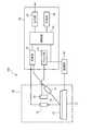
図1は、実施例1に係る欠陥検査装置のブロック図である。図1のように、欠陥検査装置100は、検査室42および処理部30を主に備えている。検査室42内には、ウエハ10を保持するステージ12、発光部14、検出部16およびカメラ20が設けられている。ステージ12は、ウエハ10を保持する。発光部14は、例えば紫外線18等をウエハ10に照射する。検出部16は、欠陥により散乱された光を検出する。ステージ12は、駆動部40によりウエハ10の表面の面方向に移動可能である。カメラ20は、ウエハ表面の画像を撮像する。 FIG. 1 is a block diagram of the defect inspection apparatus according to the first embodiment. As shown in FIG. 1, the
処理部30は、アライメント部32、検査部34、制御部36、記憶部38および出力部39を備える。アライメント部32は、カメラ20および駆動部40を用いステージ12に保持されたウエハ10のアライメントを行なう。検査部34は、検出部16が検出した光により、アライメントされたウエハ10表面の欠陥を検出する。制御部36は、アライメント部32、検査部34および駆動部40等を制御する。記憶部38は、アライメントに用いる画像または/および未検査情報を記憶する。出力部39は、未検査情報を出力する。処理部30は、例えばコンピュータまたはCPU(Central
Processing Unit)等を含む。コンピュータまたはCPU等は、プログラム等により、設定部32、検査部34、制御部36および出力部39として機能する。The
Processing Unit). The computer or the CPU functions as the
図2は、実施例1に係る欠陥検査装置の平面模式図である。欠陥検査装置100は、格納部46、搬送室44および検査室42を備えている。格納部46には、例えば複数のウエハが格納されたFOUP(Front
Open Unified Pod)またはPOD(ポッド)がセットされる。FOUPまたはPODには、例えば25枚のウエハが格納できる。格納部46が2つ設けられているため、欠陥検査装置100は、50枚のウエハを順次検査することができる。搬送室44には、搬送部が設けられている。搬送部は、ウエハをFOUPまたはPODに格納する。また、搬送部は、ウエハ10をステージ12上に搬送する。検査室42は、図1と同じであり説明を省略する。FIG. 2 is a schematic plan view of the defect inspection apparatus according to the first embodiment. The
Open Unified Pod) or POD (pod) is set. For example, 25 wafers can be stored in the FOUP or POD. Since two
次に、欠陥検出工程前後の工程の例を説明する。図3は、欠陥検出工程前後の工程を示すフローチャートである。図3のように、収納棚に、複数のウエハが収納されている(ステップS50)。例えば、50枚のウエハを1ロットとする。収納棚から1ロット分のウエハが欠陥検査装置100に自動搬送される。欠陥検査装置100において、各ウエハの欠陥を検査する(ステップS52)。欠陥検査が終了すると、各ウエハにおける欠陥のウエハ内での位置座標が欠陥検査装置100から出力される(ステップS54)。自動的または作業者の判断により、欠陥検出装置100が検出した欠陥を光学顕微鏡または電子顕微鏡を用い観察する(ステップS56)。その後、1ロット分のウエハは次の工程に進む。 Next, examples of steps before and after the defect detection step will be described. FIG. 3 is a flowchart showing steps before and after the defect detection step. As shown in FIG. 3, a plurality of wafers are stored in the storage shelf (step S50). For example, 50 lots of wafers are taken as one lot. One lot of wafers is automatically transferred from the storage shelf to the
図3のような製造工程において、欠陥検査装置100が何らかの原因でウエハの検査を行なわなかった場合、ステップS54またはS56において、ウエハの検査が行なわれていないことが判明する。この場合、再度、ウエハの欠陥検査を行なうことになる。また、ウエハが未検査の原因が分かっていないため、再度未検査となってしまうこともある。実施例1においては、このようなウエハの未検査を抑制する。 In the manufacturing process as shown in FIG. 3, if the
図4は、実施例1に係る欠陥検査装置の動作を示すフローチャートである。図4のように、ステージ12は、1枚目のウエハ10を搭載する(ステッS10)。例えば、図2の搬送室44内の搬送部がFOUPまたはPODのスロット1のウエハ10をステージ12上に搬送する。次に、アライメント部32は、カメラ20を用いステージ12に保持されたウエハ10のアライメントを行なう(以下、アライメント工程ともいう:ステップS12)。検査部34は、発光部14および検出部16を用い、ウエハ10内の欠陥を検出する(以下、欠陥検査工程ともいう:ステップS14)。例えば、制御部36は、ウエハ10内の欠陥の座標を記憶部38に記憶させる。制御部36は、アライメント工程と欠陥検査工程とが所定時間内に終了したか判定する(ステップS16)。すなわち、制御部36は、アライメント部32がウエハ10のアライメントを開始してから欠陥の検査が終了するまでの時間である検査時間が所定時間内かを判定する。Noの場合、格納部46は、ウエハ10を格納する(ステップS22)。例えば、FOUPまたはPODのスロット1にウエハ10を戻す。制御部36は、最後のウエハかを判定する(ステップS24)。例えば、格納部46内のFOUPまたはPODの全てのウエハ10の欠陥検査が終了した場合、制御部36は、Yesと判定する。 FIG. 4 is a flowchart illustrating the operation of the defect inspection apparatus according to the first embodiment. As shown in FIG. 4, the
ステップS16においてYesの場合、制御部36は、ステップS16におけるYesの判定が所定回数以内かを判定する(ステップS18)。例えば、所定回数が1回の場合、ステップS16におけるYesの判定が1回目の場合、制御部36は、Yesと判定する。ステップS16におけるYesの判定が2回目以上の場合、制御部36は、Noと判定する。このように所定回数が1回の場合、アライメント工程と欠陥検査工程のリトライは1回しか行なわない。ステップS18においてYesの場合、ステップS12に戻りアライメント工程および欠陥検査工程を再度行なう。ステップS18においてNoの場合、記憶部38は、このウエハが未検査であることを示す未検査記憶情報を記憶する(ステップS20)。その後、ステップS22に進む。 In the case of Yes in step S16, the
ステップS24においてYesの場合、制御部36は、複数のウエハのうち少なくとも1枚が未検査である情報が記憶部38に記憶されているかを判定する(ステップS26)。Yesの場合、制御部36は、出力部39を介し、未検査のウエハがあることを示すアラームおよび未検査のウエハのスロット番号を出力する(ステップS28)。その後、終了する。ステップS26においてNoの場合、終了する。その後、図3のステップS54に進む。 If Yes in step S24, the
図5(a)および図5(b)は、ウエハの平面図である。図5(a)は図4のステップS12のアライメント工程を示している。図5(a)のように、ウエハ10には、結晶方位を示すノッチ50が形成されている。ウエハ10に複数のショット領域56が形成されている。ショット領域56は、縮小露光装置において1回の露光で露光される領域である。アライメント工程においては、カメラ20が、ウエハ10内の第1領域52の画像を撮像する。記憶部38は、アライメント部32がウエハ10のアライメントを行なう際に用いるべきウエハ10内の画像を記憶している。カメラ20が撮像した画像が記憶部38に登録された画像となるようにステージ12を移動する。その後、ステージ12を移動し、カメラ20がウエハ内の第2領域54の画像を撮像する。第2領域54の画像が記憶部38に登録された画像となるようにステージ12を移動する。これにより、ウエハ10の回転方向および縦横方向の位置合わせを行なう。 5A and 5B are plan views of the wafer. FIG. 5A shows the alignment process in step S12 of FIG. As shown in FIG. 5A, the
図5(b)は図4のステップS14の欠陥検査工程を示している。図5(b)のように、欠陥検査工程では、ウエハ10内のショット領域56を矢印58のように、検査する。欠陥検査方法は、暗視野法でもよいし、明視野法でもよい。暗視野法では、発光部14がウエハ10に光を照射する。ウエハ10上に欠陥が存在すると、光が反射される。検出部16が散乱された光を検出する。これにより、欠陥の位置座標を検出することができる。明視野法では、発光部14は照明光をウエハに照射する。検出部16は、例えばカメラであり、ウエハ10表面の画像を撮像する。隣のショット領域56(またはダイ領域)との画像を比較し、異なる箇所を欠陥として検出する。発光部14が出射する光は、g線、h線またはi線のように波長の短い光を用いることができる。 FIG. 5B shows the defect inspection process in step S14 of FIG. As shown in FIG. 5B, in the defect inspection process, the
図6(a)および図6(b)は、未検査情報の例を示す図である。図6(a)のように、記憶部38には、スロットに対応する欠陥個数のテーブルが記憶されている。図4のステップS14において、欠陥検査工程が終了すると、制御部36は、検査部34が検出した欠陥の数を欠陥個数としてテーブルに入力する。例えば、図6(a)において、スロット1のウエハの欠陥個数は100であり、スロット25のウエハの欠陥個数は150である。ウエハが未検査の場合(図4のステップS18においてNoの場合)、図4のステップS20において、制御部36は、未検査情報として、欠陥個数に0を入力する。例えば、図6(a)において、スロット2のウエハの欠陥個数は0である。これは、スロット2のウエハが未検査であることを示している。図4のステップS26において、図6(a)のテーブルに欠陥個数が0のスロットがある場合、制御部36は、未検査情報があると判定することができる。 FIG. 6A and FIG. 6B are diagrams showing examples of uninspected information. As shown in FIG. 6A, the
図6(b)のテーブルにおいては、図6(a)のテーブルに加え、装置Noを記憶する項目が存在する。欠陥個数に0を入力した際に、欠陥検査を行なった欠陥検査装置のNoを入力することができる。これにより、図4のステップS28において、出力部39がアラームを出力する際に、未検査であった欠陥検査装置を特定する情報を出力することができる。未検査情報は、図6(a)および図6(b)以外にも、フラグを立てる方法など他の情報でもよい。 In the table of FIG. 6B, there is an item for storing the device number in addition to the table of FIG. When 0 is input as the number of defects, the No of the defect inspection apparatus that has performed the defect inspection can be input. Thereby, in step S28 of FIG. 4, when the
実施例1によれば、制御部36は、アライメント工程と欠陥検査工程の時間である検査時間が所定時間より短い場合(図4のステップS16のYes)、アライメント工程と欠陥検査工程とを再度行なう。すなわち、アライメント部32にウエハ10のアライメントを再度行なわせ(ステップS12)、検査部34にウエハ表面の欠陥を再度検査させる(ステップS14)。アライメント工程および欠陥検査工程が所定時間より短く終了した場合、アライメント工程または欠陥検査工程において不具合が発生し、ウエハの欠陥検査が行なわれていない可能性が高い。よって、この場合、再度アライメント工程および欠陥検査工程を行なうことにより、ウエハの未検査を抑制することができる。 According to the first embodiment, when the inspection time, which is the time between the alignment process and the defect inspection process, is shorter than the predetermined time (Yes in step S16 in FIG. 4), the
また、制御部36は、図4のステップS16においてYesの場合、ウエハ10を格納部46に格納せず、アライメント部32にアライメント工程(ステップS12)および検査部34に欠陥検査工程(ステップS14)を再度行なわせる。例えば、ウエハ10をステージ12に保持したまま、再度アライメント工程および欠陥検査工程を行なう。これにより、ウエハ10を格納部46に格納し再度取り出す時間を短縮することができる。 Further, in the case of Yes in step S16 of FIG. 4, the
さらに、制御部36は、同じウエハ10に対し所定回数以上、検査時間が所定時間より短い場合、図4のステップS20のように、ウエハ10が未検査であることを示す情報を記憶部38に記憶させる。ステップS28のように、ウエハ10が未検査であることを示す情報を外部に出力することができる。これにより、作業者は、未検査のウエハ10があることを認識することができる。これにより、早期に、欠陥検査装置に不具合があるか、ウエハに不具合があるかの調査を行なうことができる。 Further, when the inspection time is shorter than the predetermined time for the same wafer 10 a predetermined number of times or more, the
図7は、実施例2に係る欠陥検査装置の動作を示すフローチャートである。実施例1の図4と比較し、ステップS12のアライメント工程の後に、制御部36は、アライメントに用いた画像が、記憶部38に記憶されている画像と一致するか判定する(ステップS30)。Yesの場合、ステップS14の欠陥検査工程に進む。Noの場合、ステップS32に進む。ステップS16においてYesの場合もステップS32に進む。ステップS32において、制御部36は、アライメント工程を行った回数を判定する(ステップS32)。回数が1の場合、ステップS12に戻る。すなわち、再度アライメント工程を行なう。回数が2の場合、アレイメント用の画像が記憶部38に再登録済か判断する(ステップS34)。Yesの場合、ステップS20に進む。Noの場合、記憶部38にアライメト用の画像を再登録する(ステップS36)。その後ステップS12に進む。その他のステップは、実施例1の図4と同じであり説明を省略する。 FIG. 7 is a flowchart illustrating the operation of the defect inspection apparatus according to the second embodiment. Compared with FIG. 4 of the first embodiment, after the alignment step of step S12, the
実施例2によれば、図7のステップS30のように、制御部36は、アライメント部32がウエハ10をアライメントした後、アライメントに用いた画像が、記憶部38に記憶された画像と異なる場合、アライメント工程を再度行なわせる。アライメントに用いた画像が、記憶部38に記憶された画像と異なる場合、アライメントが失敗している可能性がある。このため、再度ウエハ10のアライメントを行なうことができる。 According to the second embodiment, when the
さらに、所定回数(図7の例では2回)以上、ステップS16おいてYesまたはステップS30においてNoの場合、制御部36は、アライメントに用いた画像を再登録する。例えば、再度アライメントに用いた画像を、記憶部38に記憶された画像の代わりに記憶部38に記憶させる(ステップS36)。ステップS12において、アライメント工程を再度行なわせる。同じウエハに対し所定回数以上、ステップS16のYesまたはステップS30のNoの場合、記憶部38に登録された画像がふさわしくない場合がありうる。そこで、ステップS36のように、記憶部38の画像を入れ替える。これにより、記憶部38に登録された画像がふさわしくない場合には、アライメント工程および欠陥検査工程が正常に行なわれる。 Further, when the number of times is Yes in Step S16 or No in Step S30 for a predetermined number of times (twice in the example of FIG. 7) or more, the
さらに、ステップS36を実行してから、同じウエハ10に対し所定回数(図7の例では1回)以上、ステップS16のYesまたはステップS30のNoの場合、欠陥検査装置またはウエハに不具合がある可能性が高い。そこで、制御部36は、ウエハ10が未検査であることを示す情報を出力する。例えば、これにより、早期に、欠陥検査装置に不具合があるか、ウエハに不具合があるかの調査を行なうことができる。Further, after executing step S36, if the
図8は、実施例3に係る欠陥検査装置の動作を示すフローチャートである。図8のように、実施例3は実施例1の図4に比較し、ステップS12のアライメント工程後、制御部36は、アライメント工程を開始してから所定時間内にアライメント工程が終了したかを判定する(ステップS40)。Yesの場合、ステップS18に進む。Noの場合、ステップS14に進む。その他のステップは、実施例1の図4と同じであり、説明を省略する。 FIG. 8 is a flowchart illustrating the operation of the defect inspection apparatus according to the third embodiment. As shown in FIG. 8, compared with FIG. 4 of the first embodiment, the
図9は、実施例3のタイミングチャートである。横軸は時間であり、正常、異常1、異常2および異常3の場合を示している。ハッチングされた横長の枠は、各ステップが正常に実行されていることを示している。正常な場合、格納部46からウエハ10をステージ12に保持させ、ウエハを検査室42内に搬送する。その後、アライメント工程を行なう。アライメント工程は、図5(a)において第1領域52の画像を用いてアライメント工程を行なうアライメント1工程と、第2領域54画像を用いてアライメント工程を行なうアライメント2工程と、を含んでいる。アライメント工程が終了すると、欠陥検査工程を行なう。このように、正常な場合、各シーケンスが連続して行なわれる。アライメント工程および欠陥検査工程が正常に行なわれている場合、図8のステップS40およびステップS16のいずれもNoである。よって、ステップS16においてNoの場合、欠陥検査が正常に行なわれたと判断できる。 FIG. 9 is a timing chart of the third embodiment. The horizontal axis represents time, and shows normal, abnormal 1, abnormal 2, and abnormal 3. The hatched horizontal frame indicates that each step is executed normally. When normal, the
異常1の場合、アライメント1工程とアライメント2工程との間のシーケンスがつながらず、処理が終了してしまう。この場合、図8のステップS40においてYesと判定される。よって、アライメント工程において不具合が発生したと認識できる。異常2の場合、アライメント工程と欠陥検査工程との間のシーケンスがつながらず、処理が終了してしまう。この場合、図8のステップS16においてYesと判定される。よって、欠陥検査工程において不具合が発生したと認識できる。異常3の場合、欠陥検査工程の途中で処理が終了してしまう。この場合、図8のステップS16においてYesと判定される。よって、欠陥検査工程において不具合が発生したと認識できる。未検査情報には、アライメント工程において不具合が発生したか、欠陥検査工程において不具合が発生したかの情報を含ませてもよい。 In the case of
実施例3によれば、図8のステップS40のように、制御部36は、アライメント部32がアライメントを開始してから終了するまでの時間が所定時間より短い場合、ステップS12のようにアライメント工程を再度行なわせる。これにより、アライメント工程において不具合が発生したか、欠陥検査工程において不具合が発生したか認識することができる。 According to the third embodiment, as in step S40 of FIG. 8, when the time from the start of alignment by the
なお、実施例3に実施例2のステップS30からS36を付加することもできる。 Note that steps S30 to S36 of the second embodiment can be added to the third embodiment.
実施例1から実施例3においては、欠陥検出装置が、光をウエハ10表面に照射しウエハ10表面の欠陥を検出する例を説明した。欠陥検出装置は電子線等をウエハ10表面に照射しウエハ10表面の欠陥を検出してもよい。例えば、欠陥検出装置はSEM(Scanning
Electron Microscopy)装置等でもよい。In the first to third embodiments, the example in which the defect detection apparatus detects a defect on the surface of the
Electron Microscopy) apparatus or the like may be used.
以上、本発明の実施例について詳述したが、本発明は係る特定の実施例に限定されるものではなく、特許請求の範囲に記載された本発明の要旨の範囲内において、種々の変形・変更が可能である。 Although the embodiments of the present invention have been described in detail above, the present invention is not limited to such specific embodiments, and various modifications and changes can be made within the scope of the gist of the present invention described in the claims. It can be changed.
実施例1〜3を含む実施形態に関し、さらに以下の付記を開示する。
付記1:
ウエハを保持するステージと、前記ステージに保持されたウエハのアライメントを行なうアライメント部と、アライメントされた前記ウエハ表面の欠陥を検査する検査部と、前記アライメント部が前記アライメントを開始してから前記欠陥の検査が終了するまでの時間である検査時間が所定時間より短い場合、前記アライメント部に前記アライメントを再度行なわせ、前記検査部に前記欠陥を再度検査させる制御部と、を具備することを特徴とする欠陥検査装置。
付記2:
複数のウエハを格納する格納部を具備し、前記ウエハは、前記複数のウエハのうち前記ステージに保持されたウエハであり、前記制御部は、前記検査時間が所定時間より短い場合、前記ウエハを前記格納部に格納せず、前記アライメント部に前記アライメントを再度行なわせ、前記検査部に前記欠陥を再度検査させることを特徴とする付記1記載の欠陥検出装置。
付記3:
前記制御部は、同じ前記ウエハに対し所定回数以上前記検査時間が所定時間より短い場合、前記ウエハが未検査であることを示す情報を出力することを特徴とする付記1または2記載の欠陥検出装置。
付記4:
前記アライメント部が前記ウエハのアライメントを行なう際に用いるべき前記ウエハ内の画像を記憶する記憶部を具備し、前記制御部は、前記アライメント部が前記アライメントした後、前記アライメントに用いた画像が、前記記憶部に記憶された画像と異なる場合、前記アライメント部に前記アライメントを再度行なわせることを特徴とする付記1から3のいずれか一項記載の欠陥検出装置。
付記5:
複数のウエハを格納する格納部を具備し、前記ウエハは、前記複数のウエハのうち前記ステージに保持されたウエハであり、前記複数のウエハに対応し、各ウエハが未検査であるかを示す情報を出力する出力部を具備することを特徴とする付記4記載の欠陥検出装置。
付記6:
同じ前記ウエハに対し所定回数以上前記検査時間が所定時間より短い場合、または、前記アライメントに用いた画像が、前記記憶部に記憶された画像と異なる場合、前記制御部は、再度アライメントに用いた画像を、前記記憶部に記憶された画像の代わりに記憶部に記憶させ、前記アライメント部に前記アライメントを再度行なわせることを特徴とする付記4記載の欠陥検査装置。
付記7:
前記アライメントに用いた画像を、前記記憶部に記憶された画像の代わりに記憶部に記憶させてから同じ前記ウエハに対し所定回数以上、前記検査時間が所定時間より短い場合、または、前記アライメントに用いた画像が、前記記憶部に記憶された画像と異なる場合、前記制御部は、前記ウエハが未検査であることを示す情報を出力することを特徴とする付記6記載の欠陥検査装置。
付記8:
前記制御部は、前記アライメント部が前記アライメントを開始してから終了するまでの時間が所定時間より短い場合、前記アライメント部に前記アライメントを再度行なわせる、ことを特徴とする付記1から7のいずれか一項記載の欠陥検査装置。
付記9:
前記欠陥検出装置は、光を前記ウエハ表面に照射し前記ウエハ表面の欠陥を検出することを特徴とする付記1から8のいずれか一項記載の欠陥検出装置。
付記10:
前記ステージに保持されたウエハのアライメントを行ない、アライメントされた前記ウエハ表面の欠陥を検査し、前記ウエハのアライメントを開始してから前記欠陥の検査が終了するまでの時間が所定時間より短い場合、前記アライメントおよび前記欠陥の検査を再度行なうことを特徴とする欠陥検査方法。
The following additional remarks are disclosed regarding the embodiment including Examples 1 to 3.
Appendix 1:
A stage for holding a wafer; an alignment unit for aligning the wafer held on the stage; an inspection unit for inspecting a defect on the aligned wafer surface; and the defect after the alignment unit starts the alignment. A control unit that causes the alignment unit to perform the alignment again and causes the inspection unit to inspect the defect again when the inspection time, which is the time until the inspection of is completed, is shorter than a predetermined time. Defect inspection equipment.
Appendix 2:
A storage unit configured to store a plurality of wafers, wherein the wafer is a wafer held on the stage among the plurality of wafers, and the control unit is configured to store the wafer when the inspection time is shorter than a predetermined time. 2. The defect detection apparatus according to
Appendix 3:
3. The defect detection according to
Appendix 4:
The alignment unit includes a storage unit that stores an image in the wafer to be used when performing alignment of the wafer, and the controller uses the alignment unit after the alignment unit performs the alignment. 4. The defect detection apparatus according to
Appendix 5:
A storage unit for storing a plurality of wafers is provided, and the wafers are wafers held on the stage among the plurality of wafers, and correspond to the plurality of wafers and indicate whether each wafer is uninspected. The defect detection apparatus according to appendix 4, further comprising an output unit that outputs information.
Appendix 6:
When the inspection time is shorter than the predetermined time for the same wafer, or when the image used for the alignment is different from the image stored in the storage unit, the control unit is used for the alignment again. The defect inspection apparatus according to appendix 4, wherein an image is stored in the storage unit instead of the image stored in the storage unit, and the alignment unit performs the alignment again.
Appendix 7:
When the image used for the alignment is stored in the storage unit instead of the image stored in the storage unit and the inspection time is shorter than the predetermined time for the same wafer, or for the alignment. 7. The defect inspection apparatus according to appendix 6, wherein when the used image is different from the image stored in the storage unit, the control unit outputs information indicating that the wafer is not inspected.
Appendix 8:
The control unit causes the alignment unit to perform the alignment again when the time from the start of the alignment unit to the end of the alignment is shorter than a predetermined time. The defect inspection apparatus according to
Appendix 9:
The defect detection apparatus according to any one of
Appendix 10:
When the wafer held on the stage is aligned, inspected for defects on the aligned wafer surface, and when the time from the start of wafer alignment to the end of inspection of the defects is shorter than a predetermined time, A defect inspection method, wherein the alignment and the defect inspection are performed again.
10 ウエハ
12 ステージ
32 アライメント部
34 検査部
36 制御部
38 記憶部
39 出力部
46 格納部DESCRIPTION OF
Claims (5)
Translated fromJapanese前記ウエハを保持するステージと、
前記ステージに保持された前記ウエハのアライメントを行なうアライメント部と、
アライメントされた前記ウエハ表面の欠陥を検査する検査部と、
前記複数のウエハの各ウエハについて、前記アライメント部に前記アライメントを行なわせ、前記検査部に前記欠陥を検査させ、あるウエハにおいて前記アライメント部が前記アライメントを開始してから前記欠陥の検査が終了するまでの時間である検査時間が所定時間より短い場合、前記アライメント部に前記あるウエハの前記アライメントを再度行なわせ、前記検査部に前記あるウエハの前記欠陥を再度検査させ、前記ウエハに対し2以上の所定回数以上前記検査時間が所定時間より短い場合、前記アライメント部に前記アライメントを再度行なわせずかつ前記検査部に前記欠陥を再度検査させず、前記ウエハが未検査であることを示す情報を出力する制御部と、
を具備することを特徴とする欠陥検査装置。A storage unit for storing a plurality of wafers;
A stage for holdingthe wafer,
An alignment unit for aligning the wafer held on the stage;
An inspection unit for inspecting defects on the aligned wafer surface;
For each of the plurality of wafers, the alignment unit performs the alignment, the inspection unit inspects the defect, and the inspection of the defect ends after the alignment unit starts the alignment ina certain wafer. When the inspection time, which is the time until, is shorter than a predetermined time, the alignment unit performs the alignment ofthe wafer again, causes the inspection unit to inspect the defect of thewafer again, and two or more of the wafers are inspected.If the inspection time is shorter than the predetermined time, the alignment unit does not perform the alignment again and the inspection unit does not inspect the defect again, and indicates that the wafer is uninspected. A control unit foroutputting ;
A defect inspection apparatus comprising:
前記制御部は、前記アライメント部が前記アライメントした後、前記アライメントに用いた第2画像が、前記記憶部に記憶された第1画像と異なる場合、前記アライメント部に前記アライメントを再度行なわせることを特徴とする請求項1または2記載の欠陥検査装置。Comprising a storage unit for storing afirst image of said waferto the alignment unit performs alignment of the wafer,
After the alignment unit performs the alignment, the control unit causes the alignment unit to perform the alignment again when asecond image used for the alignment is different fromthe first image stored in the storage unit. The defect inspection apparatus according to claim 1or 2, characterized in that:
ステージにウエハを保持させ、
前記ステージに保持されたウエハのアライメントを行ない、
アライメントされた前記ウエハ表面の欠陥を検査し、
あるウエハにおいてウエハのアライメントを開始してから前記欠陥の検査が終了するまでの時間が所定時間より短い場合、前記あるウエハの前記アライメントおよび前記欠陥の検査を再度行ない、
前記ウエハに対し2以上の所定回数以上前記検査時間が所定時間より短い場合、前記アライメントを再度行なわずかつ前記欠陥を再度検査せず、前記ウエハが未検査であることを示す情報を出力することを特徴とする欠陥検査方法。For each wafer of a plurality of wafers stored in the storage unit,
Hold the wafer on the stage,
Align the wafer held on the stage,
Inspect for defects on the wafer surface that has been aligned,
If the time from the start of the alignment of the wafersin one wafer to the inspection of the defects is completed is shorter than the predetermined time, again rows thathave an inspection of the alignment and the defectof the certainwafer,
When the inspection time is shorter than a predetermined time by two or more times with respect to the wafer, the alignment is not performed again and the defect is not inspected again, and information indicating that the wafer is not inspected is output. Defect inspection method characterized by
前記制御部は、前記あるウエハにおいて前記検査時間が前記所定時間より短い場合、前記あるウエハの前記アライメントに用いた第2画像を前記第1画像の代わりに前記記憶部に記憶させ、その後前記アライメント部に前記あるウエハの前記アライメントを再度行なわせ、前記検査部に前記あるウエハの前記欠陥を再度検査させる請求項1または2記載の欠陥検査装置。The alignment unit comprises a storage unit for storing a first image in the wafer for performing alignment of the wafer,
When the inspection time of the certain wafer is shorter than the predetermined time, the control unit stores the second image used for the alignment of the certain wafer in the storage unit instead of the first image, and then the alignment. The defect inspection apparatus according to claim 1, wherein the alignment of the certain wafer is performed again by a section, and the defect of the certain wafer is inspected again by the inspection section.
Priority Applications (1)
| Application Number | Priority Date | Filing Date | Title |
|---|---|---|---|
| JP2011130801AJP5742496B2 (en) | 2011-06-13 | 2011-06-13 | Defect inspection apparatus and defect inspection method |
Applications Claiming Priority (1)
| Application Number | Priority Date | Filing Date | Title |
|---|---|---|---|
| JP2011130801AJP5742496B2 (en) | 2011-06-13 | 2011-06-13 | Defect inspection apparatus and defect inspection method |
Publications (2)
| Publication Number | Publication Date |
|---|---|
| JP2013002821A JP2013002821A (en) | 2013-01-07 |
| JP5742496B2true JP5742496B2 (en) | 2015-07-01 |
Family
ID=47671565
Family Applications (1)
| Application Number | Title | Priority Date | Filing Date |
|---|---|---|---|
| JP2011130801AExpired - Fee RelatedJP5742496B2 (en) | 2011-06-13 | 2011-06-13 | Defect inspection apparatus and defect inspection method |
Country Status (1)
| Country | Link |
|---|---|
| JP (1) | JP5742496B2 (en) |
Family Cites Families (3)
| Publication number | Priority date | Publication date | Assignee | Title |
|---|---|---|---|---|
| JP4204458B2 (en)* | 2003-12-26 | 2009-01-07 | 株式会社日立ハイテクサイエンスシステムズ | Inspection method of semiconductor wafer by electron beam apparatus |
| JP2007163380A (en)* | 2005-12-15 | 2007-06-28 | Denso Corp | Visual inspection work management system |
| JP5537008B2 (en)* | 2007-11-29 | 2014-07-02 | 株式会社東芝 | Appearance inspection device |
- 2011
- 2011-06-13JPJP2011130801Apatent/JP5742496B2/ennot_activeExpired - Fee Related
Also Published As
| Publication number | Publication date |
|---|---|
| JP2013002821A (en) | 2013-01-07 |
Similar Documents
| Publication | Publication Date | Title |
|---|---|---|
| JP5287178B2 (en) | Defect review device | |
| US8711348B2 (en) | Method of inspecting wafer | |
| KR20230111273A (en) | Method for inspecting substrate, substrate treatment system, and computer storage medium | |
| US20180005370A1 (en) | Substrate defect inspection apparatus, method of adjusting sensitivity parameter value for substrate defect inspection, and non-transitory storage medium | |
| KR100882252B1 (en) | Defect inspection device and defect inspection method | |
| JP6092602B2 (en) | Defect inspection apparatus and defect inspection method | |
| CN109752390B (en) | Inspection equipment and inspection method for detecting defects in photomasks and die | |
| TW200816343A (en) | Defect inspecting method and defect inspecting apparatus | |
| JP7730890B2 (en) | Manufacturing method, inspection method, and inspection device | |
| JP2018514760A (en) | How to test electronic components | |
| US8914754B2 (en) | Database-driven cell-to-cell reticle inspection | |
| KR100862883B1 (en) | Semiconductor device in-tray inspection device and inspection method using the same | |
| JP4595881B2 (en) | Surface inspection device | |
| JP2009150718A (en) | Inspection device and inspection program | |
| JP5742496B2 (en) | Defect inspection apparatus and defect inspection method | |
| JP5212779B2 (en) | Surface inspection apparatus and surface inspection method | |
| US20030156749A1 (en) | Pattern inspecting apparatus and pattern inspecting method | |
| TWI780973B (en) | Inspection method and inspection system of electron beam inspection image | |
| JP5148564B2 (en) | Appearance inspection method and appearance inspection apparatus for inspecting using the method | |
| US8625090B2 (en) | Method and apparatus for inspecting substrates | |
| KR100997882B1 (en) | Wafer Pattern Inspection Method | |
| KR20220134611A (en) | Systems and methods for semiconductor device printed inspection alignment | |
| JP2008032702A (en) | Defect inspecting device and method | |
| WO2012135513A1 (en) | Method of manufacturing semiconductor devices | |
| JP2009180710A (en) | Method and apparatus for determining detection sensitivity for pattern inspection |
Legal Events
| Date | Code | Title | Description |
|---|---|---|---|
| A621 | Written request for application examination | Free format text:JAPANESE INTERMEDIATE CODE: A621 Effective date:20140303 | |
| A131 | Notification of reasons for refusal | Free format text:JAPANESE INTERMEDIATE CODE: A131 Effective date:20141021 | |
| A977 | Report on retrieval | Free format text:JAPANESE INTERMEDIATE CODE: A971007 Effective date:20141022 | |
| A521 | Written amendment | Free format text:JAPANESE INTERMEDIATE CODE: A523 Effective date:20141113 | |
| TRDD | Decision of grant or rejection written | ||
| A01 | Written decision to grant a patent or to grant a registration (utility model) | Free format text:JAPANESE INTERMEDIATE CODE: A01 Effective date:20150407 | |
| A61 | First payment of annual fees (during grant procedure) | Free format text:JAPANESE INTERMEDIATE CODE: A61 Effective date:20150420 | |
| R150 | Certificate of patent or registration of utility model | Ref document number:5742496 Country of ref document:JP Free format text:JAPANESE INTERMEDIATE CODE: R150 | |
| S531 | Written request for registration of change of domicile | Free format text:JAPANESE INTERMEDIATE CODE: R313531 | |
| R350 | Written notification of registration of transfer | Free format text:JAPANESE INTERMEDIATE CODE: R350 | |
| LAPS | Cancellation because of no payment of annual fees |