JP5741296B2 - Communication device - Google Patents
Communication deviceDownload PDFInfo
- Publication number
- JP5741296B2 JP5741296B2JP2011168641AJP2011168641AJP5741296B2JP 5741296 B2JP5741296 B2JP 5741296B2JP 2011168641 AJP2011168641 AJP 2011168641AJP 2011168641 AJP2011168641 AJP 2011168641AJP 5741296 B2JP5741296 B2JP 5741296B2
- Authority
- JP
- Japan
- Prior art keywords
- signal
- pulse
- return zero
- communication apparatus
- pulse generator
- Prior art date
- Legal status (The legal status is an assumption and is not a legal conclusion. Google has not performed a legal analysis and makes no representation as to the accuracy of the status listed.)
- Expired - Fee Related
Links
Images


Classifications
- H—ELECTRICITY
- H04—ELECTRIC COMMUNICATION TECHNIQUE
- H04B—TRANSMISSION
- H04B1/00—Details of transmission systems, not covered by a single one of groups H04B3/00 - H04B13/00; Details of transmission systems not characterised by the medium used for transmission
- H04B1/69—Spread spectrum techniques
- H04B1/7163—Spread spectrum techniques using impulse radio
- H04B1/717—Pulse-related aspects
- H04B1/7174—Pulse generation
- H—ELECTRICITY
- H04—ELECTRIC COMMUNICATION TECHNIQUE
- H04B—TRANSMISSION
- H04B1/00—Details of transmission systems, not covered by a single one of groups H04B3/00 - H04B13/00; Details of transmission systems not characterised by the medium used for transmission
- H04B1/69—Spread spectrum techniques
- H04B1/7163—Spread spectrum techniques using impulse radio
- H04B1/719—Interference-related aspects
- H—ELECTRICITY
- H04—ELECTRIC COMMUNICATION TECHNIQUE
- H04B—TRANSMISSION
- H04B10/00—Transmission systems employing electromagnetic waves other than radio-waves, e.g. infrared, visible or ultraviolet light, or employing corpuscular radiation, e.g. quantum communication
- H04B10/25—Arrangements specific to fibre transmission
- H04B10/2507—Arrangements specific to fibre transmission for the reduction or elimination of distortion or dispersion
- H04B10/2513—Arrangements specific to fibre transmission for the reduction or elimination of distortion or dispersion due to chromatic dispersion
- H04B10/25137—Arrangements specific to fibre transmission for the reduction or elimination of distortion or dispersion due to chromatic dispersion using pulse shaping at the transmitter, e.g. pre-chirping or dispersion supported transmission [DST]
- H—ELECTRICITY
- H04—ELECTRIC COMMUNICATION TECHNIQUE
- H04L—TRANSMISSION OF DIGITAL INFORMATION, e.g. TELEGRAPHIC COMMUNICATION
- H04L25/00—Baseband systems
- H04L25/02—Details ; arrangements for supplying electrical power along data transmission lines
- H04L25/03—Shaping networks in transmitter or receiver, e.g. adaptive shaping networks
- H04L25/03828—Arrangements for spectral shaping; Arrangements for providing signals with specified spectral properties
- H04L25/03834—Arrangements for spectral shaping; Arrangements for providing signals with specified spectral properties using pulse shaping
- H—ELECTRICITY
- H04—ELECTRIC COMMUNICATION TECHNIQUE
- H04L—TRANSMISSION OF DIGITAL INFORMATION, e.g. TELEGRAPHIC COMMUNICATION
- H04L25/00—Baseband systems
- H04L25/38—Synchronous or start-stop systems, e.g. for Baudot code
- H04L25/40—Transmitting circuits; Receiving circuits
- H04L25/49—Transmitting circuits; Receiving circuits using code conversion at the transmitter; using predistortion; using insertion of idle bits for obtaining a desired frequency spectrum; using three or more amplitude levels ; Baseband coding techniques specific to data transmission systems
- H04L25/4904—Transmitting circuits; Receiving circuits using code conversion at the transmitter; using predistortion; using insertion of idle bits for obtaining a desired frequency spectrum; using three or more amplitude levels ; Baseband coding techniques specific to data transmission systems using self-synchronising codes, e.g. split-phase codes
- H—ELECTRICITY
- H04—ELECTRIC COMMUNICATION TECHNIQUE
- H04L—TRANSMISSION OF DIGITAL INFORMATION, e.g. TELEGRAPHIC COMMUNICATION
- H04L25/00—Baseband systems
- H04L25/38—Synchronous or start-stop systems, e.g. for Baudot code
- H04L25/40—Transmitting circuits; Receiving circuits
- H04L25/49—Transmitting circuits; Receiving circuits using code conversion at the transmitter; using predistortion; using insertion of idle bits for obtaining a desired frequency spectrum; using three or more amplitude levels ; Baseband coding techniques specific to data transmission systems
- H04L25/4906—Transmitting circuits; Receiving circuits using code conversion at the transmitter; using predistortion; using insertion of idle bits for obtaining a desired frequency spectrum; using three or more amplitude levels ; Baseband coding techniques specific to data transmission systems using binary codes
- H04L25/4915—Transmitting circuits; Receiving circuits using code conversion at the transmitter; using predistortion; using insertion of idle bits for obtaining a desired frequency spectrum; using three or more amplitude levels ; Baseband coding techniques specific to data transmission systems using binary codes using pattern inversion or substitution
Landscapes
- Engineering & Computer Science (AREA)
- Computer Networks & Wireless Communication (AREA)
- Signal Processing (AREA)
- Physics & Mathematics (AREA)
- Spectroscopy & Molecular Physics (AREA)
- Electromagnetism (AREA)
- Power Engineering (AREA)
- Transmitters (AREA)
Description
Translated fromJapanese本発明は、通信装置に関する。 The present invention relates to a communication device.
インパルス無線通信は、短パルスを用いた無線通信であり、広帯域無線通信システムへの適用が期待されている。 Impulse wireless communication is wireless communication using short pulses, and is expected to be applied to a broadband wireless communication system.
また、ユニポーラ信号をバイポーラ信号に変換するU/B変換回路であって、入力NRZ信号をNRZ/RZ変換した信号を与えたとき、トランジスタのエミッタ出力にNRZ信号を変換したバイポーラ信号を得るU/B変換回路が知られている(例えば、特許文献1参照)。 The U / B converter circuit converts a unipolar signal into a bipolar signal, and when a signal obtained by converting the input NRZ signal into an NRZ / RZ signal is applied, a U / B for obtaining a bipolar signal obtained by converting the NRZ signal into the emitter output of the transistor. A B conversion circuit is known (see, for example, Patent Document 1).
また、差動トランジスタ対が2段縦積みされ、入力データの値に対応して単極パルスを両極パルスに変換するパルス極性変調回路が知られている(例えば、特許文献2参照)。 Further, there is known a pulse polarity modulation circuit in which differential transistor pairs are vertically stacked and convert a monopolar pulse into a bipolar pulse in accordance with the value of input data (see, for example, Patent Document 2).
本発明の目的は、送信信号内の輝線スペクトルを除去することができる通信装置を提供することである。 The objective of this invention is providing the communication apparatus which can remove the bright line spectrum in a transmission signal.
通信装置は、データ信号の値に応じたパルスの有無であって正極パルス及び負極パルスを交互に生成するパルス発生部と、前記パルス発生部により生成されたパルスをフィルタリングするバンドパスフィルタと、前記バンドパスフィルタによりフィルタリングされた信号を増幅して送信信号として出力する送信増幅器とを有し、前記データ信号の送信速度は、前記バンドパスフィルタの通過上限周波数と通過下限周波数との差の整数分の1である。The communication device includes a pulse generator that alternately generates a positive pulse and a negative pulse depending on the value of a data signal, a bandpass filter that filters the pulse generated by the pulse generator, havea transmission amplifier that outputs a transmission signal by amplifying the filtered signal by the band-passfilter, the transmission rate of the data signal is an integer fraction of the difference between the passage upper limit frequency and the pass limit frequency of the band-
正極パルス及び負極パルスを交互に生成することにより、送信信号内の輝線スペクトルを除去することができる。By generating the positive pulse and the negative pulse alternately, the bright line spectrum in the transmission signal can be removed.
図1(A)は実施形態によるインパルス無線通信装置の構成例を示す図であり、図1(B)はバンドパスフィルタ103の通過周波数帯域を示す図である。インパルス無線通信装置は、ベースバンド信号生成器101、短パルス発生部102、バンドパスフィルタ103、送信増幅器104、第1のアンテナ105、第2のアンテナ121、受信増幅器122、検波器123、リミットアンプ124及びベースバンド信号再生器125を有する。ベースバンド信号生成器101、短パルス発生部102、バンドパスフィルタ103、送信増幅器104及び第1のアンテナ105は、送信部を構成する。これに対し、第2のアンテナ121、受信増幅器122、検波器123、リミットアンプ124及びベースバンド信号再生器125は、受信部を構成する。 FIG. 1A is a diagram illustrating a configuration example of the impulse radio communication device according to the embodiment, and FIG. 1B is a diagram illustrating a pass frequency band of the
まず、送信部について説明する。ベースバンド信号生成器101は、タイムスロット単位のデータ信号A1を生成し、短パルス発生部102に出力する。図7に示すように、データ信号A1は、「1」の値ではハイレベルになり、「0」の値ではローレベルになる。データ信号A1の通信速度は例えば10ギガビット/秒(Gbps)である。短パルス発生器部102は、データ信号A1がタイムスロットでハイレベルになると、短パルスA6を生成する。バンドパスフィルタ103は、短パルスA6に対して所定の通過周波数帯域のみを通過させるためのフィルタリングを行い、ミリ波パルスA7を出力する。 First, the transmission unit will be described. The
図1(B)は、バンドパスフィルタ103の通過周波数帯域132を示す。短パルス特性131は、短パルスA6の周波数特性を示す。ミリ波パルスA7は、短パルス特性131のうちの通過周波数帯域132の部分のみの周波数成分を有する。UWB(超広帯域無線:Ultra Wide Band)等では、使用可能な周波数帯域が制限されている。その周波数帯域の制限を満たすようにするために、バンドパスフィルタ103を用いる。通過周波数帯域132は、例えば、通過下限周波数f1が80GHz、通過上限周波数f2が90GHzであり、通過周波数帯域幅がf2−f1=90−80=10GHzである。 FIG. 1B shows a
送信増幅器104は、ミリ波パルスA7を増幅し、第1のアンテナ105を介して、送信信号A8を無線送信する。送信信号A8は、ミリ波パルスの有無により、「1」又は「0」のデータを表す。 The
次に、受信部について説明する。受信増幅器122は、第2のアンテナ121を介して、受信信号を無線受信し、増幅する。検波器123は、受信増幅器122により増幅された受信信号(ミリ波パルス)の包絡線を検波して出力する。リミットアンプ124は、検波器123により検波された信号を増幅する。ベースバンド信号再生器125は、リミットアンプ124により増幅された信号を入力し、例えば10Gbpsの受信データの再生を行う。 Next, the receiving unit will be described. The
インパルス方式の無線通信装置は、マイクロ波帯、準ミリ波帯、UWBをはじめとする超広帯域無線通信装置に利用可能である。インパルス方式は、狭帯域通信方式と比較して、発振器やミキサが不要でRF部の構成が簡素・低コストとなる特徴を有し、広帯域を利用できるミリ波帯においては10Gbpsを超える広帯域無線通信の実現が期待される。 The impulse radio communication apparatus can be used for an ultra-wideband radio communication apparatus such as a microwave band, a quasi-millimeter wave band, and UWB. Compared to narrowband communication systems, the impulse system does not require an oscillator or mixer, and has a feature that the configuration of the RF unit is simple and low-cost. Broadband wireless communication exceeding 10 Gbps in the millimeter wave band where a wideband can be used Realization of is expected.
インパルス無線通信装置に割り当てられた周波数帯域幅をBmaxとすれば、バンドパスフィルタ103の通過周波数帯域幅BbpfがBmaxと等しいとき、最大通信速度Bmaxを得る。例えば、周波数帯域幅Bmaxが10GHzの場合、図1(B)に示すように、バンドパスフィルタ103の通過周波数帯域幅Bbpfはf2−f1=90−80=10GHzであり、データ信号の通信速度は10Gbpsである。 If the frequency bandwidth allocated to the impulse radio communication device is Bmax, the maximum communication speed Bmax is obtained when the pass frequency bandwidth Bbpf of the
図2(A)は、短パルス発生部102がユニポーラ短パルスB6を生成する例を示す図である。短パルス発生器102は、データ信号A1がハイレベルのタイムスロットでは正極性短パルスを生成し、データ信号A1がローレベルのタイムスロットでは正極性短パルスを生成せず、ユニポーラ短パルスB6を出力する。ユニポーラ短パルスB6は、単極性(例えば正極性)の短パルスである。バンドパスフィルタ103は、ユニポーラ短パルスB6をフィルタリングし、ミリ波パルスB7を出力する。例えば、ミリ波パルスB7は、その通信速度が10Gbpsであり、そのタイムスロットが100psである。 FIG. 2A is a diagram illustrating an example in which the
図2(B)は図2(A)のミリ波パルスB7の周波数スペクトルを示す図であり、図2(C)は図2(B)の一部の拡大図である。ミリ波パルスB7の通信速度が10Gbpsの場合、10GHz間隔で、輝線スペクトルBLが発生する。輝線スペクトルBLは、線状の大電力のスペクトルであり、例えば、30、40、50、60、70、80、90GHz等で発生している。輝線スペクトルBLは、通信速度に等しい周波数間隔で現れる。例えば、輝線スペクトルBLは、通信速度が10Gbpsの場合、10GHz間隔で出現することになる。 2B is a diagram showing a frequency spectrum of the millimeter wave pulse B7 in FIG. 2A, and FIG. 2C is an enlarged view of a part of FIG. 2B. When the communication speed of the millimeter wave pulse B7 is 10 Gbps, the bright line spectrum BL is generated at intervals of 10 GHz. The bright line spectrum BL is a linear high-power spectrum and is generated at, for example, 30, 40, 50, 60, 70, 80, 90 GHz. The bright line spectrum BL appears at a frequency interval equal to the communication speed. For example, the bright line spectrum BL appears at 10 GHz intervals when the communication speed is 10 Gbps.
ところで、多くの無線通信装置は、例えば周波数1MHz当たりの信号強度0dBm(=1mW/MHz)というように、法令や規格などで、単位周波数当りの信号強度(電力スペクトル密度)が規定される。送信信号に輝線スペクトルBLが含まれると、輝線スペクトルBLの信号強度が上記の電力スペクトル密度の制限にかかって、全周波数帯域での平均電力を上げられないという事態が生じる。具体的には、割り当てられた周波数帯域Bmaxが10GHz(=10000MHz)のとき、送信スペクトル強度が周波数帯域内で一定であれば、1(mW/MHz)×10000(MHz)=10Wの出力が可能となるが、送信信号に1mW/MHzの輝線スペクトルBLが含まれる場合、小さな電力しか出せない。信号を誤りなく長距離送信するためには、全周波数帯域のスペクトル電力を最大限大きくして、雑音等に対する信号強度マージン(SN比)を確保する必要がある。送信電力が輝線スペクトルBLで制限されると、SN比を十分確保できない。このように、輝線スペクトルBLにより送信電力が制限され、長距離・高品質通信が不利となるため、輝線スペクトルBLの生じないインパルス無線通信装置の実現が課題である。以下、送信信号に輝線スペクトルBLを含まず、長距離・高品質通信に適したインパルス無線通信装置の実施形態を説明する。 By the way, in many wireless communication devices, for example, the signal strength (power spectral density) per unit frequency is defined by laws and standards such as a signal strength of 0 dBm (= 1 mW / MHz) per frequency of 1 MHz. When the transmission line includes the bright line spectrum BL, the signal intensity of the bright line spectrum BL is limited by the power spectral density, and the average power in the entire frequency band cannot be increased. Specifically, when the assigned frequency band Bmax is 10 GHz (= 10000 MHz) and the transmission spectrum intensity is constant within the frequency band, an output of 1 (mW / MHz) × 10000 (MHz) = 10 W is possible. However, when the transmission signal includes the bright line spectrum BL of 1 mW / MHz, only a small amount of power can be output. In order to transmit a signal over a long distance without error, it is necessary to maximize the spectrum power in the entire frequency band to ensure a signal strength margin (SN ratio) against noise or the like. If the transmission power is limited by the bright line spectrum BL, the SN ratio cannot be secured sufficiently. As described above, transmission power is limited by the bright line spectrum BL, and long-distance / high-quality communication is disadvantageous. Therefore, it is a problem to realize an impulse radio communication device that does not generate the bright line spectrum BL. Hereinafter, an embodiment of an impulse radio communication apparatus suitable for long-distance / high-quality communication without including the bright line spectrum BL in the transmission signal will be described.
図3は、ユニポーラ短パルスB6及びバイポーラ短パルスA6の例を示す図である。ユニポーラ短パルスB6は、図2(A)のユニポーラ短パルスB6と同様である。本実施形態では、短パルス発生部102は、データ信号A1を入力し、バイポーラ短パルスA6を生成する。バイポーラ短パルスA6は、データ信号A1の値に応じたパルスの有無であって正極パルス及び負極パルスを交互に生成されるパルスである。例えば、バイポーラ短パルスA6は、データ信号A1の値が「1」のときに正極パルス又は負極パルスが発生し、データ信号A1の値が「0」のときに基準電圧となる。正極パルスは基準電圧に対して正電圧のパルスであり、負極パルスは基準電圧に対して負電圧のパルスである。すなわち、バイポーラ短パルスA6は、直前のパルスに対して逆極性のパルスになる。 FIG. 3 is a diagram illustrating examples of the unipolar short pulse B6 and the bipolar short pulse A6. The unipolar short pulse B6 is the same as the unipolar short pulse B6 in FIG. In the present embodiment, the
バイポーラ短パルスA6は、ユニポーラ短パルスB6に対して、高周波成分の位相が反転するだけであり、信号の包絡線が同じになる。図1(A)の検波器123は、受信信号の包絡線を検波する。したがって、図1(A)のインパルス無線通信装置の受信部は、ユニポーラ短パルスB6を受信する場合でも、バイポーラ短パルスA6を受信する場合でも同じ構成でよい。 The bipolar short pulse A6 only has the phase of the high frequency component inverted with respect to the unipolar short pulse B6, and the signal envelope is the same. The
図4(A)は、バイポーラ短パルスA6の電力スペクトル密度を示す図である。ここで、送信信号の通信速度は10Gbpsであり、送信信号のタイムスロットは100psである。バイポーラ短パルスA6の電力スペクトル密度では、通信速度(10Gbps)の整数倍に等しい周波数でノッチが生じる。すなわち、kを整数とすると、k×10GHzの周波数でノッチが生じる。ノッチは、電力スペクトル密度が小さくなる凹部である。 FIG. 4A is a diagram showing the power spectral density of the bipolar short pulse A6. Here, the transmission speed of the transmission signal is 10 Gbps, and the time slot of the transmission signal is 100 ps. In the power spectral density of the bipolar short pulse A6, a notch occurs at a frequency equal to an integral multiple of the communication speed (10 Gbps). That is, when k is an integer, a notch is generated at a frequency of k × 10 GHz. The notch is a recess that reduces the power spectral density.
図4(B)は、ユニポーラ短パルスB6を入力したバンドパスフィルタ103の出力信号の電力スペクトル密度を示す図である。ユニポーラ短パルスB6の場合、図2(B)及び(C)と同様に、通信速度(10Gbps)の整数倍に等しい周波数で輝線スペクトルBLが生じる。例えば、60GHz、70GHz及び80GHzで輝線スペクトルBLが生じる。 FIG. 4B is a diagram illustrating the power spectral density of the output signal of the
図4(C)は、バイポーラ短パルスA6を入力したバンドパスフィルタ103の出力信号A7の電力スペクトル密度を示す図である。バイポーラ短パルスA6の場合、図4(A)と同様に、通信速度(10Gbps)の整数倍に等しい周波数でノッチが生じる。例えば、60GHz、70GHz及び80GHzでノッチが生じる。その結果、通信速度(10Gbps)の整数倍に等しい周波数における輝線スペクトルBLが除去される。本実施形態によれば、輝線スペクトルBLが生じないので、送信電力の確保が容易となり、長距離・高品質通信を行うのに有利となる。さらに、割り当てられた周波数帯域に対して、適切な通信速度を設定することにより、バンドパスフィルタ103の通過周波数帯域の両端f1及びf2にノッチを配置することができるので、割り当て周波数帯域外への不要電波の放射を抑制するのにも有利となる。 FIG. 4C is a diagram illustrating the power spectral density of the output signal A7 of the
データ信号の送信速度は、バンドパスフィルタ103の通過上限周波数f2と通過下限周波数f1との差の整数分の1に設定する。例えば、上限周波数f2は90GHz、下限周波数f1は80GHzである。バンドパスフィルタ103の通過周波数帯域幅は、f2−f1=90−80=10GHzである。この場合、データ信号の送信速度は、10GHzの整数分の1に設定する。例えば、データ信号の送信速度は、10Gbps、5Gbps、2Gbps又は1Gbps等に設定することができる。このように送信速度を設定することにより、バンドパスフィルタ103の通過周波数帯域の両端f1及びf2にノッチを配置することができるので、割り当て周波数帯域外への不要電波の放射を抑制することができる。なお、送信速度を遅くする程、ノッチの周波数間隔が短くなり、ノッチの数が増える。 The transmission speed of the data signal is set to 1 / integer of the difference between the pass upper limit frequency f2 and the pass lower limit frequency f1 of the
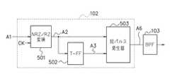
図5は図1(A)の短パルス発生部102の構成例を示す図であり、図7は短パルス発生部102の動作例を説明するためのタイミングチャートである。短パルス発生部102は、ノンリターンゼロ(NRZ)/リターンゼロ(RZ)変換部501、トリガフリップフロップ(T−FF)502及び短パルス発生器503を有する。データ信号A1は、ノンリターンゼロ信号である。ノンリターンゼロ/リターンゼロ変換部501は、ノンリターンゼロ信号A1をリターンゼロ信号A2に変換する。具体的には、ノンリターンゼロ/リターンゼロ変換部501は、論理積(AND)回路であり、ノンリターンゼロ信号A1及びクロック信号CKの論理積をとり、その論理積信号をリターンゼロ信号A2として出力する。トリガフリップフロップ502は、リターンゼロ信号A2が1周期変化する毎に出力信号A3を反転させる。例えば、リターンゼロ信号A2がハイレベル→ローレベル→ハイレベルのように1周期変化する毎に、出力信号A3は論理レベルが反転する。具体的には、出力信号A3は、リターンゼロ信号A2の立ち上がりエッジに同期して論理反転する。短パルス発生器503は、トリガフリップフロップ502の出力信号A3及びリターンゼロ信号A2を入力し、リターンゼロ信号A2のパルス幅を短くし、かつ正極パルス及び負極パルスを交互に生成した信号A6をバンドパスフィルタ103に出力する。 FIG. 5 is a diagram illustrating a configuration example of the short
図6は、図5の短パルス発生器503の構成例を示す回路図である。遅延回路601は、リターンゼロ信号A2を遅延させた信号A4を出力する。抵抗602は、グランド電位ノード及び信号/A5のノード間に接続される。抵抗603は、グランド電位ノード及び信号A5のノード間に接続される。信号A5及び/A5は、相互に位相が反転した差動信号である。nチャネル電界効果トランジスタ604は、ドレインが信号/A5のノードに接続され、ゲートがバイアス電位ノードに接続され、ソースがnチャネル電界効果トランジスタ606のドレインに接続される。nチャネル電界効果トランジスタ605は、ドレインが信号A5のノードに接続され、ゲートがバイアス電位ノードに接続され、ソースがnチャネル電界効果トランジスタ607のドレインに接続される。nチャネル電界効果トランジスタ606は、ゲートがリターンゼロ信号A2のノードに接続され、ソースがnチャネル電界効果トランジスタ610のドレインに接続される。nチャネル電界効果トランジスタ607は、ゲートが例えば−2Vの電位ノードに接続され、ソースがnチャネル電界効果トランジスタ610のドレインに接続される。トランジスタ604及び605は、それぞれゲート接地カスコード増幅器を構成する。nチャネル電界効果トランジスタ610は、ゲートが信号A4のノードに接続され、ソースがnチャネル電界効果トランジスタ612のドレインに接続される。 FIG. 6 is a circuit diagram showing a configuration example of the
nチャネル電界効果トランジスタ608は、ドレインがnチャネル電界効果トランジスタ606のドレインに接続され、ゲートが例えば−1.7Vの電位ノードに接続され、ソースがnチャネル電界効果トランジスタ611のドレインに接続される。nチャネル電界効果トランジスタ609は、ドレインがnチャネル電界効果トランジスタ607のドレインに接続され、ゲートが例えば−2.3Vの電位ノードに接続され、ソースがnチャネル電界効果トランジスタ611のドレインに接続される。nチャネル電界効果トランジスタ611は、ゲートが例えば−2.4Vの電位ノードに接続され、ソースがnチャネル電界効果トランジスタ612のドレインに接続される。nチャネル電界効果トランジスタ612は、電流源であり、ゲートがバイアス電位ノードに接続され、ソースが例えば−2.6Vの電位ノードに接続される。 In the n-channel
抵抗613は、グランド電位ノード及び信号A6のノード間に接続される。抵抗614は、グランド電位ノード及び信号/A6のノード間に接続される。信号A6及び/A6は、相互に位相が反転した差動信号である。nチャネル電界効果トランジスタ615は、ドレインが信号A6のノードに接続され、ゲートが信号A3のノードに接続され、ソースがnチャネル電界効果トランジスタ619のドレインに接続される。nチャネル電界効果トランジスタ616は、ドレインが信号/A6のノードに接続され、ゲートが信号/A3のノードに接続され、ソースがnチャネル電界効果トランジスタ619のドレインに接続される。信号A3及び/A3は、相互に位相が反転した差動信号である。nチャネル電界効果トランジスタ619は、ゲートが信号/A5のノードに接続され、ソースがnチャネル電界効果トランジスタ621のドレインに接続される。 The
nチャネル電界効果トランジスタ617は、ドレインが信号A6のノードに接続され、ゲートがバイアス電位ノードに接続され、ソースがnチャネル電界効果トランジスタ620のドレインに接続される。nチャネル電界効果トランジスタ618は、ドレインが信号/A6のノードに接続され、ゲートがバイアス電位ノードに接続され、ソースがnチャネル電界効果トランジスタ620のドレインに接続される。nチャネル電界効果トランジスタ620は、ゲートが信号A5のノードに接続され、ソースがnチャネル電界効果トランジスタ621のドレインに接続される。nチャネル電界効果トランジスタ621は、電流源であり、ゲートがバイアス電位ノードに接続され、ソースが例えば−2.6Vの電位ノードに接続される。 In the n-channel
信号A5は、リターンゼロ信号A2及び遅延信号A4の論理積信号である。信号A3がハイレベルのときに信号A5がハイレベルパルスになると、信号A6は正極パルスになる。これに対し、信号A3がローレベルのときに信号A5がハイレベルパルスになると、信号A6は負極パルスになる。バイポーラ短パルスA6は、例えば基準電圧が−0.4Vであり、0Vの正極パルス及び−0.8Vの負極パルスが交互に生成される。 The signal A5 is a logical product signal of the return zero signal A2 and the delay signal A4. If the signal A5 becomes a high level pulse when the signal A3 is at a high level, the signal A6 becomes a positive pulse. On the other hand, if the signal A5 becomes a high level pulse when the signal A3 is at a low level, the signal A6 becomes a negative pulse. In the bipolar short pulse A6, for example, the reference voltage is -0.4V, and a positive pulse of 0V and a negative pulse of -0.8V are alternately generated.
本実施形態によれば、送信信号に輝線スペクトルBLが含まれないため、輝線スペクトルBLによる電力制限を受けることなく、大きな送信電力を確保して大きな通信マージン(S/N)を得ることができ、信号の長距離・高品質通信が容易になるという効果がある。また、割り当てられた周波数帯域に対し、通信速度を適切に設定し、割り当て周波数帯域幅の両端にスペクトルのノッチを配置することにより、割り当て周波数帯域外への不要電力放射を低減するという効果も有する。受信部において、バイポーラ短パルスA6を受信するための受信部は、ユニポーラ短パルスB6を受信するための受信部に対して、同様の構成にすることができるため、導入コストの増大も最小限に抑えられる。 According to this embodiment, since the transmission line does not include the bright line spectrum BL, a large communication margin (S / N) can be obtained by securing a large transmission power without being limited by the power of the bright line spectrum BL. This has the effect of facilitating long-distance / high-quality communication of signals. Also, it has the effect of reducing unnecessary power radiation outside the allocated frequency band by appropriately setting the communication speed for the allocated frequency band and arranging spectral notches at both ends of the allocated frequency bandwidth. . In the receiving unit, the receiving unit for receiving the bipolar short pulse A6 can have the same configuration as the receiving unit for receiving the unipolar short pulse B6, so that the increase in introduction cost is also minimized. It can be suppressed.
なお、上記実施形態は、何れも本発明を実施するにあたっての具体化の例を示したものに過ぎず、これらによって本発明の技術的範囲が限定的に解釈されてはならないものである。すなわち、本発明はその技術思想、又はその主要な特徴から逸脱することなく、様々な形で実施することができる。 The above-described embodiments are merely examples of implementation in carrying out the present invention, and the technical scope of the present invention should not be construed in a limited manner. That is, the present invention can be implemented in various forms without departing from the technical idea or the main features thereof.
101 ベースバンド信号生成器
102 短パルス発生部
103 バンドパスフィルタ
104 送信増幅器
105 第1のアンテナ
121 第2のアンテナ
122 受信増幅器
123 検波器
124 リミットアンプ
125 ベースバンド信号再生器101
Claims (9)
Translated fromJapanese前記パルス発生部により生成されたパルスをフィルタリングするバンドパスフィルタと、
前記バンドパスフィルタによりフィルタリングされた信号を増幅して送信信号として出力する送信増幅器とを有し、
前記データ信号の送信速度は、前記バンドパスフィルタの通過上限周波数と通過下限周波数との差の整数分の1であることを特徴とする通信装置。A pulse generator that alternately generates a positive pulse and a negative pulse in the presence or absence of a pulse according to the value of the data signal;
A bandpass filter for filtering the pulses generated by the pulse generator;
Havea transmission amplifier that outputs a transmission signal by amplifying the filtered signal by the band-passfilter,
The communication apparatus according to claim1, wherein a transmission speed of the data signal is an integral number of a difference between a pass upper limit frequency and a pass lower limit frequency of the band pass filter .
前記パルス発生器は、前記トリガフリップフロップの出力信号及び前記リターンゼロ信号を入力することを特徴とする請求項3記載の通信装置。The pulse generator includes a trigger flip-flop that inverts an output signal every time the return zero signal changes by one cycle,
4. The communication apparatus according to claim 3, wherein the pulse generator inputs an output signal of the trigger flip-flop and the return zero signal.
前記データ信号をノンリターンゼロ信号からリターンゼロ信号に変換するノンリターンゼロ/リターンゼロ変換部と、
前記リターンゼロ信号のパルス幅を短くし、かつ正極パルス及び負極パルスを交互に生成するパルス発生器とを有することを特徴とする請求項1記載の通信装置。The pulse generator is
A non-return zero / return zero converter for converting the data signal from a non-return zero signal to a return zero signal;
The communication apparatus according to claim 1, further comprising: a pulse generator that shortens a pulse width of the return zero signal and alternately generates a positive pulse and a negative pulse.
前記パルス発生器は、前記トリガフリップフロップの出力信号及び前記リターンゼロ信号を入力することを特徴とする請求項5記載の通信装置。The pulse generator includes a trigger flip-flop that inverts an output signal every time the return zero signal changes by one cycle,
6. The communication apparatus according to claim 5, wherein the pulse generator inputs an output signal of the trigger flip-flop and the return zero signal.
前記受信増幅器により増幅された受信信号を検波する検波器とを有することを特徴とする請求項1〜7のいずれか1項に記載の通信装置。A receiving amplifier that amplifies the received signal;
The communication apparatus according to any one of claims 1 to7, characterized in that it has a detector for detecting the received signal amplified by the receiving amplifier.
前記受信増幅器は、前記第2のアンテナにより無線受信した受信信号を増幅することを特徴とする請求項8記載の通信装置。And a second antenna for wirelessly receiving the received signal,
The communication apparatus according to claim8 , wherein the reception amplifier amplifies a reception signal wirelessly received by the second antenna.
Priority Applications (3)
| Application Number | Priority Date | Filing Date | Title |
|---|---|---|---|
| JP2011168641AJP5741296B2 (en) | 2011-08-01 | 2011-08-01 | Communication device |
| EP12177938.3AEP2555440B1 (en) | 2011-08-01 | 2012-07-26 | Impulse radio communication apparatus |
| US13/559,883US9184789B2 (en) | 2011-08-01 | 2012-07-27 | Communication apparatus |
Applications Claiming Priority (1)
| Application Number | Priority Date | Filing Date | Title |
|---|---|---|---|
| JP2011168641AJP5741296B2 (en) | 2011-08-01 | 2011-08-01 | Communication device |
Publications (2)
| Publication Number | Publication Date |
|---|---|
| JP2013034075A JP2013034075A (en) | 2013-02-14 |
| JP5741296B2true JP5741296B2 (en) | 2015-07-01 |
Family
ID=46796255
Family Applications (1)
| Application Number | Title | Priority Date | Filing Date |
|---|---|---|---|
| JP2011168641AExpired - Fee RelatedJP5741296B2 (en) | 2011-08-01 | 2011-08-01 | Communication device |
Country Status (3)
| Country | Link |
|---|---|
| US (1) | US9184789B2 (en) |
| EP (1) | EP2555440B1 (en) |
| JP (1) | JP5741296B2 (en) |
Families Citing this family (5)
| Publication number | Priority date | Publication date | Assignee | Title |
|---|---|---|---|---|
| JP5790519B2 (en)* | 2012-01-26 | 2015-10-07 | 富士通株式会社 | Communication device |
| JP5991243B2 (en)* | 2013-03-18 | 2016-09-14 | 富士通株式会社 | Transmitter |
| JP2014195216A (en)* | 2013-03-29 | 2014-10-09 | Nippon Telegr & Teleph Corp <Ntt> | Communication system and communication method |
| JP2014195217A (en)* | 2013-03-29 | 2014-10-09 | Nippon Telegr & Teleph Corp <Ntt> | Communication system and communication method |
| JP6149937B2 (en) | 2013-10-02 | 2017-06-21 | 富士通株式会社 | Pulse position modulation type impulse radio transmitter and radio communication system |
Family Cites Families (20)
| Publication number | Priority date | Publication date | Assignee | Title |
|---|---|---|---|---|
| US4419757A (en)* | 1981-03-16 | 1983-12-06 | Bell Telephone Laboratories, Incorporated | Transformerless bipolar converter |
| US4504944A (en)* | 1982-05-13 | 1985-03-12 | At&T Bell Laboratories | Bridging channel port module |
| CA1288822C (en)* | 1987-05-29 | 1991-09-10 | Yoshitoshi Murata | Radio communication network system comprising a connecting equipment unit operable in different modes |
| JP2725058B2 (en) | 1989-06-26 | 1998-03-09 | 富士通株式会社 | U / B conversion circuit |
| US5365551A (en)* | 1992-12-15 | 1994-11-15 | Micron Technology, Inc. | Data communication transceiver using identification protocol |
| JP3152292B2 (en)* | 1997-04-15 | 2001-04-03 | 日本電気株式会社 | Method and apparatus for removing multi-channel echo |
| US6020765A (en)* | 1997-05-30 | 2000-02-01 | Sun Microsystems, Inc. | Frequency difference detector for use with an NRZ signal |
| US6218842B1 (en)* | 1999-08-04 | 2001-04-17 | Halliburton Energy Services, Inc. | Multi-frequency electromagnetic wave resistivity tool with improved calibration measurement |
| US6665500B2 (en)* | 2001-01-29 | 2003-12-16 | Oyster Optics, Inc. | Dual-mode fiber optic telecommunications system and method |
| WO2003088568A2 (en)* | 2002-04-12 | 2003-10-23 | Thomson Licensing S.A. | Digital control circuit for serial uart transmissions |
| JP3705271B2 (en)* | 2003-02-03 | 2005-10-12 | ソニー株式会社 | Transmission method and transmission apparatus |
| US7298792B2 (en)* | 2003-02-10 | 2007-11-20 | Mitsubishi Electric Research Laboratories, Inc. | Randomly changing pulse polarity and phase in an UWB signal for power spectrum density shaping |
| US7636380B2 (en)* | 2004-05-17 | 2009-12-22 | Microsoft Corporation | Orthogonal pulse polarity modulation |
| US20060066485A1 (en)* | 2004-09-24 | 2006-03-30 | Guohua Min | Wireless tracking system based upon phase differences |
| JP3943569B2 (en) | 2004-11-30 | 2007-07-11 | 富士通株式会社 | Pulse polarity modulation circuit |
| JP4408091B2 (en)* | 2005-04-18 | 2010-02-03 | 日本電信電話株式会社 | Wireless transmission method and wireless transmitter |
| JP4350133B2 (en)* | 2007-02-19 | 2009-10-21 | 富士通株式会社 | Transmission circuit and wireless transmission device |
| US8332680B2 (en)* | 2007-08-13 | 2012-12-11 | Rambus Inc. | Methods and systems for operating memory in two modes |
| US20110141829A1 (en)* | 2009-12-14 | 2011-06-16 | Ware Frederick A | Circuits for Reducing Power Consumption of Memory Components |
| US8867930B2 (en)* | 2010-10-29 | 2014-10-21 | Queen's University At Kingston | System and method for determining the envelope of a modulated signal |
- 2011
- 2011-08-01JPJP2011168641Apatent/JP5741296B2/ennot_activeExpired - Fee Related
- 2012
- 2012-07-26EPEP12177938.3Apatent/EP2555440B1/ennot_activeNot-in-force
- 2012-07-27USUS13/559,883patent/US9184789B2/ennot_activeExpired - Fee Related
Also Published As
| Publication number | Publication date |
|---|---|
| US20130034131A1 (en) | 2013-02-07 |
| JP2013034075A (en) | 2013-02-14 |
| US9184789B2 (en) | 2015-11-10 |
| EP2555440B1 (en) | 2016-05-25 |
| EP2555440A1 (en) | 2013-02-06 |
Similar Documents
| Publication | Publication Date | Title |
|---|---|---|
| JP5790519B2 (en) | Communication device | |
| KR100944774B1 (en) | Transmission circuit and wireless transmission device | |
| JP5741296B2 (en) | Communication device | |
| KR20120061398A (en) | Method and apparatus for generating pulse | |
| JP5104712B2 (en) | Transmitter | |
| US8437377B2 (en) | Pulse generator, transmitter-receiver, and pulse generation method | |
| JP6149937B2 (en) | Pulse position modulation type impulse radio transmitter and radio communication system | |
| WO2014207866A1 (en) | Pulse generator, semiconductor integrated circuit, and wireless data transmission method | |
| JP5367861B2 (en) | Ultra-wideband wireless communication device | |
| JP5041406B2 (en) | Ultra-wideband wireless communication device | |
| Majidzadeh et al. | An 8-PPM, 45 pJ/bit UWB transmitter with reduced number of PA elements | |
| JP5459369B2 (en) | Transmitter | |
| JP5077147B2 (en) | Signal generator | |
| Daoud et al. | Design of an OOK IR-UWB front-end for biomedical devices | |
| JP2016086309A (en) | Bipolar impulse radio communication system, bipolar impulse transmitter and receiver | |
| JP4444781B2 (en) | Radio transmitter, transmission signal power adjustment device, and transmission signal power adjustment method | |
| JP6164101B2 (en) | Demodulator, receiver and impulse radio communication system | |
| JP2017028656A (en) | Impulse transmitter, impulse receiver and impulse radio communication system | |
| JP2019036894A (en) | Impulse wireless communication apparatus and impulse wireless communication system | |
| Vaithianathan et al. | Design and simulation of pulse generator for Ultra Wide Band impulse radio | |
| JP2006115217A (en) | Wireless transmission method and wireless transmitter | |
| Chen et al. | Fully integrated CMOS UWB transmitter for application in China | |
| Hajri et al. | Study of non-coherent transceivers for UWB communication |
Legal Events
| Date | Code | Title | Description |
|---|---|---|---|
| A621 | Written request for application examination | Free format text:JAPANESE INTERMEDIATE CODE: A621 Effective date:20140404 | |
| A977 | Report on retrieval | Free format text:JAPANESE INTERMEDIATE CODE: A971007 Effective date:20150116 | |
| A131 | Notification of reasons for refusal | Free format text:JAPANESE INTERMEDIATE CODE: A131 Effective date:20150120 | |
| A521 | Request for written amendment filed | Free format text:JAPANESE INTERMEDIATE CODE: A523 Effective date:20150312 | |
| TRDD | Decision of grant or rejection written | ||
| A01 | Written decision to grant a patent or to grant a registration (utility model) | Free format text:JAPANESE INTERMEDIATE CODE: A01 Effective date:20150331 | |
| A61 | First payment of annual fees (during grant procedure) | Free format text:JAPANESE INTERMEDIATE CODE: A61 Effective date:20150413 | |
| R150 | Certificate of patent or registration of utility model | Ref document number:5741296 Country of ref document:JP Free format text:JAPANESE INTERMEDIATE CODE: R150 | |
| LAPS | Cancellation because of no payment of annual fees |