JP5709718B2 - Light emitting device - Google Patents
Light emitting deviceDownload PDFInfo
- Publication number
- JP5709718B2 JP5709718B2JP2011223050AJP2011223050AJP5709718B2JP 5709718 B2JP5709718 B2JP 5709718B2JP 2011223050 AJP2011223050 AJP 2011223050AJP 2011223050 AJP2011223050 AJP 2011223050AJP 5709718 B2JP5709718 B2JP 5709718B2
- Authority
- JP
- Japan
- Prior art keywords
- light emitting
- support substrate
- emitting element
- electrode
- heat sink
- Prior art date
- Legal status (The legal status is an assumption and is not a legal conclusion. Google has not performed a legal analysis and makes no representation as to the accuracy of the status listed.)
- Active
Links
- 239000000758substrateSubstances0.000claimsdescription89
- 239000004065semiconductorSubstances0.000claimsdescription42
- 239000013078crystalSubstances0.000claimsdescription28
- 239000002114nanocompositeSubstances0.000claimsdescription27
- 239000002184metalSubstances0.000claimsdescription17
- 229910052751metalInorganic materials0.000claimsdescription17
- 229910045601alloyInorganic materials0.000claimsdescription8
- 239000000956alloySubstances0.000claimsdescription8
- 238000005266castingMethods0.000claimsdescription2
- 125000004432carbon atomChemical groupC*0.000claims1
- 239000010410layerSubstances0.000description42
- OKTJSMMVPCPJKN-UHFFFAOYSA-NCarbonChemical compound[C]OKTJSMMVPCPJKN-UHFFFAOYSA-N0.000description25
- 230000017525heat dissipationEffects0.000description25
- 239000002041carbon nanotubeSubstances0.000description22
- 229910021393carbon nanotubeInorganic materials0.000description22
- 239000010949copperSubstances0.000description12
- 239000000463materialSubstances0.000description12
- 229910052802copperInorganic materials0.000description11
- 239000004020conductorSubstances0.000description9
- RYGMFSIKBFXOCR-UHFFFAOYSA-NCopperChemical compound[Cu]RYGMFSIKBFXOCR-UHFFFAOYSA-N0.000description8
- 239000002131composite materialSubstances0.000description6
- 230000000694effectsEffects0.000description6
- 230000020169heat generationEffects0.000description6
- 238000000034methodMethods0.000description6
- 150000001721carbonChemical group0.000description4
- 238000004519manufacturing processMethods0.000description4
- 239000002105nanoparticleSubstances0.000description4
- 238000007747platingMethods0.000description4
- XUIMIQQOPSSXEZ-UHFFFAOYSA-NSiliconChemical compound[Si]XUIMIQQOPSSXEZ-UHFFFAOYSA-N0.000description3
- 230000008901benefitEffects0.000description3
- 230000006866deteriorationEffects0.000description3
- 238000005304joiningMethods0.000description3
- 238000002844meltingMethods0.000description3
- 238000004806packaging method and processMethods0.000description3
- 229910052710siliconInorganic materials0.000description3
- 239000010703siliconSubstances0.000description3
- 229910052718tinInorganic materials0.000description3
- XMWRBQBLMFGWIX-UHFFFAOYSA-NC60 fullereneChemical compoundC12=C3C(C4=C56)=C7C8=C5C5=C9C%10=C6C6=C4C1=C1C4=C6C6=C%10C%10=C9C9=C%11C5=C8C5=C8C7=C3C3=C7C2=C1C1=C2C4=C6C4=C%10C6=C9C9=C%11C5=C5C8=C3C3=C7C1=C1C2=C4C6=C2C9=C5C3=C12XMWRBQBLMFGWIX-UHFFFAOYSA-N0.000description2
- 238000010521absorption reactionMethods0.000description2
- 238000000149argon plasma sinteringMethods0.000description2
- 230000015572biosynthetic processEffects0.000description2
- 229910052799carbonInorganic materials0.000description2
- 150000001875compoundsChemical class0.000description2
- 230000008878couplingEffects0.000description2
- 238000010168coupling processMethods0.000description2
- 238000005859coupling reactionMethods0.000description2
- 238000002425crystallisationMethods0.000description2
- 230000008025crystallizationEffects0.000description2
- 229910003460diamondInorganic materials0.000description2
- 239000010432diamondSubstances0.000description2
- 238000001803electron scatteringMethods0.000description2
- 229910003472fullereneInorganic materials0.000description2
- 229910052737goldInorganic materials0.000description2
- 229910052738indiumInorganic materials0.000description2
- 239000004973liquid crystal related substanceSubstances0.000description2
- 239000011159matrix materialSubstances0.000description2
- 230000008018meltingEffects0.000description2
- VNWKTOKETHGBQD-UHFFFAOYSA-NmethaneChemical compoundCVNWKTOKETHGBQD-UHFFFAOYSA-N0.000description2
- 239000000203mixtureSubstances0.000description2
- 239000002048multi walled nanotubeSubstances0.000description2
- 230000003287optical effectEffects0.000description2
- 230000000149penetrating effectEffects0.000description2
- 230000001737promoting effectEffects0.000description2
- 230000005855radiationEffects0.000description2
- 229910052709silverInorganic materials0.000description2
- 239000002109single walled nanotubeSubstances0.000description2
- 239000007787solidSubstances0.000description2
- 229910000521B alloyInorganic materials0.000description1
- 229910018104Ni-PInorganic materials0.000description1
- 229910018536Ni—PInorganic materials0.000description1
- OAICVXFJPJFONN-UHFFFAOYSA-NPhosphorusChemical compound[P]OAICVXFJPJFONN-UHFFFAOYSA-N0.000description1
- 230000002159abnormal effectEffects0.000description1
- 230000009471actionEffects0.000description1
- 239000000853adhesiveSubstances0.000description1
- 230000001070adhesive effectEffects0.000description1
- 229910052782aluminiumInorganic materials0.000description1
- 229910052787antimonyInorganic materials0.000description1
- 229910052797bismuthInorganic materials0.000description1
- 230000015556catabolic processEffects0.000description1
- 239000000919ceramicSubstances0.000description1
- 230000008859changeEffects0.000description1
- 229910052804chromiumInorganic materials0.000description1
- 238000006731degradation reactionMethods0.000description1
- 238000009792diffusion processMethods0.000description1
- 238000009429electrical wiringMethods0.000description1
- 230000002349favourable effectEffects0.000description1
- 239000010419fine particleSubstances0.000description1
- 229910021389grapheneInorganic materials0.000description1
- 238000010438heat treatmentMethods0.000description1
- 230000001771impaired effectEffects0.000description1
- 238000002347injectionMethods0.000description1
- 239000007924injectionSubstances0.000description1
- 229910000765intermetallicInorganic materials0.000description1
- 239000007769metal materialSubstances0.000description1
- 238000012986modificationMethods0.000description1
- 230000004048modificationEffects0.000description1
- 239000002159nanocrystalSubstances0.000description1
- 229910052759nickelInorganic materials0.000description1
- 239000011368organic materialSubstances0.000description1
- 229910052763palladiumInorganic materials0.000description1
- 230000035515penetrationEffects0.000description1
- 230000002093peripheral effectEffects0.000description1
- 229910052697platinumInorganic materials0.000description1
- 239000000843powderSubstances0.000description1
- 230000008569processEffects0.000description1
- 230000001681protective effectEffects0.000description1
- 239000003870refractory metalSubstances0.000description1
- 239000011347resinSubstances0.000description1
- 229920005989resinPolymers0.000description1
- 238000005096rolling processMethods0.000description1
- 229910052594sapphireInorganic materials0.000description1
- 239000010980sapphireSubstances0.000description1
- 239000002356single layerSubstances0.000description1
- 230000005476size effectEffects0.000description1
- 238000007711solidificationMethods0.000description1
- 230000008023solidificationEffects0.000description1
- 238000004544sputter depositionMethods0.000description1
- 239000000126substanceSubstances0.000description1
- 239000011800void materialSubstances0.000description1
Images


Landscapes
- Led Device Packages (AREA)
Description
Translated fromJapanese本発明は、発光デバイスに関する。 The present invention relates to a light emitting device.
発光ダイオードを用いた発光デバイスは、省エネルギー、長寿命という利点があり、照明装置、カラー画像表示装置、液晶パネルのバックライト、又は、交通信号灯などの光源として、注目されている。 A light-emitting device using a light-emitting diode has advantages of energy saving and long life, and has attracted attention as a light source such as a lighting device, a color image display device, a liquid crystal panel backlight, or a traffic signal light.
この種の発光デバイスについて、従来は、フリップ・チップ(FC)として構成されたLEDチップをサブマウント基板に実装し、更に、この組み立て体をパッケージング基板に実装し、サブマウント基板に形成された電極と、パッケージング基板に形成された電極とを、ワイヤ・ボンディングによって接続していた。 For this type of light emitting device, conventionally, an LED chip configured as a flip chip (FC) is mounted on a submount substrate, and this assembly is further mounted on a packaging substrate and formed on the submount substrate. The electrode and the electrode formed on the packaging substrate were connected by wire bonding.
しかし、この組み立て構造では、AlN等の高価な材料で構成されたサブマウント基板を使用しなければならいことから、コスト高になる。しかも、サブマウント基板に形成された電極と、パッケージング基板に形成された電極とを、ワイヤ・ボンディングによって接続する必要があるため、ワイヤボンダ装置・ワイヤボンディング装置が必要であり、生産設備費が増大し、それが製品コストに転嫁され、発光デバイスのコスト高を招いていた。 However, this assembly structure increases the cost because a submount substrate made of an expensive material such as AlN must be used. In addition, since the electrodes formed on the submount substrate and the electrodes formed on the packaging substrate must be connected by wire bonding, a wire bonder device and a wire bonding device are required, which increases production equipment costs. However, this has been passed on to the product cost, leading to high costs for light emitting devices.
上述した問題点を解決する手段として、特許文献1には、シリコン・サブマウントの一面に溝を形成し、その溝底部に2つのビア(貫通電極)を形成し、LEDダイスを、溝内にフリップ・チップ・マウントし、保護接着剤で溝を充填するLEDパッケージの製造方法が開示されている。 As means for solving the above-described problems,
しかしながら、LEDダイスの発光動作時に発生した熱を逃がす放熱構造については、全く考慮されていない。このため、LEDダイスに発生した熱によって、LEDダイスとビアとを接続する接合部分の接合強度が失われ、電気的接続の信頼性が損なわれたり、あるいは、LEDダイスの発光特性が変動してしまうという惧れがある。そのような問題を回避するためには、LEDに供給する電流を低下させて、発熱量を低減しなければならず、そうすると、発光量が低下してしまう。 However, no consideration is given to a heat dissipation structure that releases heat generated during the light emitting operation of the LED die. For this reason, due to the heat generated in the LED die, the bonding strength of the bonding portion connecting the LED die and the via is lost, the reliability of the electrical connection is impaired, or the light emission characteristics of the LED die are changed. There is a fear that it will end. In order to avoid such a problem, it is necessary to reduce the amount of heat generated by reducing the current supplied to the LED.
放熱構造については、特許文献2〜5に記載されたものが知られている。まず、特許文献2には、光反射層の内側面に接続された伝熱導体層と、基板本体の裏面との間に配置された伝熱ビア導体を、基板本体の裏面に形成されたパッドに接続した構造が開示されている。パッドは、伝熱ビア導体毎に個別に独立して備えられるものであるので、面積が小さく、熱容量が小さいから、それ自体では高い放熱特性を確保することができない。 About the heat dissipation structure, what was described in patent documents 2-5 is known. First, in Patent Document 2, a heat transfer via conductor disposed between a heat transfer conductor layer connected to an inner surface of a light reflection layer and a back surface of a substrate body is provided with a pad formed on the back surface of the substrate body. A structure connected to is disclosed. Since the pads are individually provided for each heat transfer via conductor, the pads have a small area and a small heat capacity, so that high heat dissipation characteristics cannot be secured by themselves.
次に、特許文献3は、発光素子サブマウント構造体を、配線基板を兼ねる第1の放熱用基板に搭載し、発光素子サブマウント構造体の第1の放熱用基板に面する側とは異なる側の面を、第2の放熱用基板に接触または接合した放熱構造が開示されている。しかし、この特許文献3の構造は、実装基板の内部に蓄積された熱の放熱に不向きである。特許文献3には、複数のサーマルビアを設ける構造が開示されているが、サーマルビアの一端部は、内蔵された配線パッドに接続されていて、その一部が外部に引き出されているにすぎないから、優れた放熱特性を確保することが困難である。 Next, in
特許文献4は、基板にスルーホール導熱体を設ける構造を開示しているが、導熱体の一端は電極やパッド等の小面積導体に接続されており、やはり、十分な放熱特性を確保することが困難である。
特許文献5では、シリコン基板の他表面側に、シリコン基板よりも熱伝導率の高い金属材料からなる矩形状の放熱用パッド部を形成し、ダイパッド部と放熱用パッド部とを、Cuなどからなる複数のサーマルビアを介して熱的に結合し、LEDチップで発生した熱を、サーマルビアおよび放熱用パッド部を介して放熱されるようになっている。しかし、この放熱構造では、LEDチップで発生した熱を、その直下方向に放熱するにとどまり、全周方向に拡散する熱に対しては、サーマルビアによる放熱効果を期待することができない。 In Patent Document 5, a rectangular heat dissipating pad portion made of a metal material having a higher thermal conductivity than the silicon substrate is formed on the other surface side of the silicon substrate, and the die pad portion and the heat dissipating pad portion are made of Cu or the like. The heat generated by the LED chip is thermally radiated through the thermal via and the heat radiating pad portion. However, in this heat dissipation structure, the heat generated in the LED chip is only dissipated in the direction directly below, and the heat dissipation effect due to the thermal via cannot be expected for the heat diffused in the entire circumferential direction.
本発明の課題は、放熱性に優れ、発光動作時の発熱によって、接合強度が低下したり、或いは、発光特性が変動するといった問題を生じにくい信頼性の高い発光デバイスを提供することである。 An object of the present invention is to provide a highly reliable light-emitting device that has excellent heat dissipation and is less likely to cause problems such as a decrease in bonding strength or a change in light-emitting characteristics due to heat generation during a light-emitting operation.
本発明のもう1つの課題は、発生した光を、効率よく外部に放射させ得る発光デバイスを提供することである。 Another object of the present invention is to provide a light emitting device capable of efficiently emitting generated light to the outside.
上述した課題を解決するため、本発明に係る発光デバイスは、支持基板と、発光素子とを含む。前記支持基板は、2つの貫通電極と、複数の柱状ヒートシンクとを含み、一面に凹部を有している。前記貫通電極のそれぞれは、前記支持基板を厚み方向に貫通し、一端が前記凹部の内面に露出している。前記柱状ヒートシンクは、前記支持基板の厚み方向に設けられ、所定の占有率をもって分布している。前記発光素子は、P型半導体層及びN型半導体層を積層した構造を含み、前記支持基板の前記凹部内に配置され、前記P型半導体層のP側電極が、前記貫通電極の一方の前記一端に接続され、前記N型半導体層のN側電極が、前記貫通電極の他方の前記一端に接続されている。 In order to solve the above-described problem, a light-emitting device according to the present invention includes a support substrate and a light-emitting element. The support substrate includes two through electrodes and a plurality of columnar heat sinks, and has a recess on one surface. Each of the through electrodes penetrates the support substrate in the thickness direction, and one end is exposed on the inner surface of the recess. The columnar heat sinks are provided in the thickness direction of the support substrate and are distributed with a predetermined occupation ratio. The light-emitting element includes a structure in which a P-type semiconductor layer and an N-type semiconductor layer are stacked, and is disposed in the concave portion of the support substrate, and a P-side electrode of the P-type semiconductor layer is one of the through electrodes. Connected to one end, the N-side electrode of the N-type semiconductor layer is connected to the other end of the through electrode.
上述したように、本発明に係る発光デバイスは、支持基板を含んでおり、この支持基板は、複数の柱状ヒートシンクを含んでいる。柱状ヒートシンクは、支持基板の厚み方向に設けられている。したがって、発光素子の発光動作によって生じた熱を、柱状ヒートシンクによって、支持基板の外部に放熱し、発光素子と貫通電極とを接続する接合部分の接合強度を保存し、電気的接続の信頼性を維持することができる。また、発熱による発光素子の発光特性の変動を回避することができる。 As described above, the light emitting device according to the present invention includes a support substrate, and the support substrate includes a plurality of columnar heat sinks. The columnar heat sink is provided in the thickness direction of the support substrate. Therefore, the heat generated by the light emitting operation of the light emitting element is radiated to the outside of the support substrate by the columnar heat sink, and the bonding strength of the bonding portion connecting the light emitting element and the through electrode is preserved, and the reliability of the electrical connection is improved. Can be maintained. In addition, fluctuations in the light emission characteristics of the light emitting element due to heat generation can be avoided.
柱状ヒートシンクは、所定の占有率をもって分布している。したがって、柱状ヒートシンクを構成する材料の熱抵抗、及び、柱状ヒートシンクの占有率を適切に選ぶことにより、発光素子の発光動作によって生じた熱を、柱状ヒートシンクによって、支持基板の外部に効率よく放熱しえる。 The columnar heat sinks are distributed with a predetermined occupation ratio. Therefore, by appropriately selecting the thermal resistance of the material constituting the columnar heat sink and the occupation ratio of the columnar heat sink, the heat generated by the light emitting operation of the light emitting element is efficiently radiated to the outside of the support substrate by the column heat sink. Yeah.
本発明に係る発光デバイスにおいて、支持基板は、2つの貫通電極を含み、一面に凹部を有している。貫通電極のそれぞれは、支持基板を厚み方向に貫通し、一端が凹部の内面に露出している。この支持基板の凹部内に発光素子が配置されている。発光素子は、P型半導体層及びN型半導体層を積層した構造である。そして、凹部の内部で、P型半導体層のP側電極が貫通電極の一方の一端に接続され、N型半導体層のN側電極が、貫通電極の他方の一端に接続されている。したがって、本発明によれば、発光素子のための電極が、光出射面に現れない構造が実現できる。よって、発生した光を、効率よく外部に放射させ得る。 In the light emitting device according to the present invention, the support substrate includes two through electrodes and has a recess on one surface. Each of the through electrodes penetrates the support substrate in the thickness direction, and one end is exposed on the inner surface of the recess. A light emitting element is disposed in the recess of the support substrate. The light emitting element has a structure in which a P-type semiconductor layer and an N-type semiconductor layer are stacked. Inside the recess, the P-side electrode of the P-type semiconductor layer is connected to one end of the through electrode, and the N-side electrode of the N-type semiconductor layer is connected to the other end of the through electrode. Therefore, according to the present invention, a structure in which the electrode for the light emitting element does not appear on the light emitting surface can be realized. Therefore, the generated light can be efficiently emitted to the outside.
柱状ヒートシンクは、その一端が、支持基板の他面側に導出され、支持基板の他面に設けられた放熱体に接続されていることが好ましい。この構造によれば、放熱特性が更に向上する。 It is preferable that one end of the columnar heat sink is led to the other surface side of the support substrate and connected to a heat radiator provided on the other surface of the support substrate. According to this structure, the heat dissipation characteristics are further improved.
好ましくは、凹部の内面と発光素子の側面との間に、反射膜が設けられる。これにより、PN接合によって生じた光の散乱・吸収作用を抑えながら、これを光出射面に導くことができる。 Preferably, a reflective film is provided between the inner surface of the recess and the side surface of the light emitting element. As a result, it is possible to guide the light to the light exit surface while suppressing the light scattering / absorption effect caused by the PN junction.
反射膜は、凹部の内面に付着されていてもよいし、発光素子の側面に付着されていてもよい。また、発光素子は、好ましくは、凹部に対して嵌めこまれている。この構造によれば、支持基板に対する発光素子の位置決め・配置を、容易かつ確実に実行することができる。 The reflective film may be attached to the inner surface of the recess, or may be attached to the side surface of the light emitting element. Further, the light emitting element is preferably fitted in the recess. According to this structure, the positioning and arrangement of the light emitting elements with respect to the support substrate can be performed easily and reliably.
好ましくは、前記貫通電極及び前記柱状ヒートシンクの少なくとも一方は、nmサイズの炭素原子構造体を含有するナノコンポジット構造を有し、前記支持基板に設けられたビアを鋳型とする鋳込み成形体でなる。Preferably, at least one of the through electrode and the columnar heat sink has a nanocomposite structure containing a nanometer-sized carbon atom structure, and is a cast-molded body using a via provided in the supportsubstrate as a mold.
本発明において、nmサイズとは1μm以下の範囲をいう。また、ナノコンポジット構造とは、少なくとも2種の組成分が一体となって複合体を構成し、それらの組成分が、nmサイズの微粒子、または、ナノ結晶もしくはナノアモルファスの相となっているものをいう。 In the present invention, the nm size means a range of 1 μm or less. In addition, the nanocomposite structure is a composite in which at least two kinds of components are integrated to form a composite, and these components are nano-sized fine particles, or a nanocrystal or nanoamorphous phase. Say.
上述したように、貫通電極及び柱状ヒートシンクの少なくとも一方が、基板に設けられたビアを鋳型とする鋳込み成形体であると、ビアの側壁面に対する密着力が高く、巣、空隙、空洞のない緻密な構造を持ち、電気抵抗の小さな貫通電極、熱伝導性に優れた柱状ヒートシンクを有する支持基板が得られる。ビアの内壁面に凹凸があっても、貫通電極及び柱状ヒートシンクは、その凹凸に倣うように鋳込まれるから、ビアに対する密着強度の高い貫通電極及び柱状ヒートシンクが得られる。As described above, when at least one of the through electrode and the columnar heat sink is a cast molded body using a via provided in the substrate as a mold, the adhesion to the side wall surface of the via is high, and there is no dense, void, or cavity. Thus, a supportsubstrate having a through-electrode with a small electrical resistance and a columnar heat sink excellent in thermal conductivity can be obtained. Even if the inner wall surface of the via is uneven, the through electrode and the columnar heat sink are cast so as to follow the unevenness, so that the through electrode and the columnar heat sink having high adhesion strength to the via can be obtained.
しかも、貫通電極及び柱状ヒートシンクが、ビアの内壁面の凹凸に倣うように鋳込まれる結果、貫通電極及び柱状ヒートシンクとビアの内壁面の凹凸が、貫通電極及び柱状ヒートシンクの抜けを阻止するアンカー部として働くので、支持基板に対する貫通電極及び柱状ヒートシンクの接合強度が高くなる。このことは、めっきによって貫通電極を形成する場合と異なって、ビアの内壁面に凹凸精度が要求されず、むしろ、若干の凹凸があった方が好ましい結果になるということを意味する。このため、ビアの形成が容易になる。In addition, the through electrode and the columnar heat sink are cast so as to follow the irregularities of the inner wall surface of the via. Therefore, the bonding strength of the through electrode and the columnar heat sink to the supportsubstrate is increased. This means that unlike the case where the through electrode is formed by plating, the inner wall surface of the via is not required to have unevenness accuracy, but rather it is preferable that there is a slight unevenness. For this reason, formation of a via becomes easy.
貫通電極は、複数であるから、支持基板に搭載される発光素子に対して、貫通電極を、正極及び負極として活用することができる。このため、ワイヤボンディング等の電気配線が不要になり、高価なワイヤボンディング装置等に費やされていた生産設備費をカットし、製品コストを低減させることができる。Since there are a plurality of through electrodes, the through electrodes can be used as a positive electrode and a negative electrode for the light emitting element mounted on the supportsubstrate . This eliminates the need for electrical wiring such as wire bonding, cuts the production equipment cost spent on expensive wire bonding apparatuses and the like, and reduces product costs.
更に、貫通電極及び柱状ヒートシンクの少なくとも一方は、炭素原子構造体含有するナノコンポジット構造である。炭素原子構造体は、ダイヤモンド、フラーレンまたはカーボンナノチューブから選択された少なくとも一種を含有する。その中でも、カーボンナノチューブが適している。nmサイズのカーボンナノチューブ(Carbon nanotube)を含有するナノコンポジット構造を有することができる。カーボンナノチューブは、銅の10倍の高熱伝導特性を有する。したがって、放熱特性の極めて優れた柱状ヒートシンクを実現することができる。 Furthermore, at least one of the through electrode and the columnar heat sink has a nanocomposite structure containing a carbon atom structure. The carbon atomic structure contains at least one selected from diamond, fullerene or carbon nanotube. Among these, carbon nanotubes are suitable. It can have a nanocomposite structure containing nanometer-sized carbon nanotubes. Carbon nanotubes have 10 times higher thermal conductivity than copper. Therefore, it is possible to realize a columnar heat sink having extremely excellent heat dissipation characteristics.
また、カーボンナノチューブは、電流密度耐性が、109A/cm2で、銅の1,000倍以上の高電流密度耐性を有する。しかも、カーボンナノチューブ内では、電気良導体の銅との対比において、電子散乱が少ないため、電気抵抗が小さい。したがって、カーボンナノチューブを含有するによれば、銅との対比において、電気抵抗が小さく、大きな電流を流しても、抵抗発熱量を低減することができる。The carbon nanotube has a current density resistance of 109 A / cm2 and a high current density resistance of 1,000 times or more that of copper. In addition, in the carbon nanotube, since the electron scattering is small in comparison with copper, which is a good electrical conductor, the electrical resistance is small. Therefore, when carbon nanotubes are contained, the resistance heating value can be reduced even when a large electric current is passed in comparison with copper, since the electric resistance is small.
ナノコンポジット構造を有する貫通電極及び柱状ヒートシンクは、nmサイズ効果として、応力が小さくなる。このため、半導体支持基板において、半導体回路の特性劣化が抑制される。また、支持基板に亀裂・クラックが入るのを抑制することもできる。The through electrode having a nanocomposite structure and the columnar heat sink have a smaller stress due to the nm size effect. For this reason, in the semiconductor supportsubstrate , the characteristic deterioration of the semiconductor circuit is suppressed. Moreover, it can also suppress that a crack and a crack enter into a supportsubstrate .
貫通電極及び柱状ヒートシンクは、nmサイズのカーボンナノチューブと、ナノコンポジット結晶構造の金属/合金成分を含むナノコンポジット構造としてもよい。nmサイズのカーボンナノチューブと、ナノコンポジット結晶構造の金属/合金成分を含むナノコンポジット構造の貫通電極は、大きさが、ナノレベルに制限された組織(結晶)を含むから、その効果として、貫通電極及び柱状ヒートシンクに発生する応力が小さくなる。しかも、ナノコンポジット結晶構造には、縦導体の等軸晶化を促進する働きもある。上述したナノコンポジット結晶構造及びナノコンポジット構造の有する特有の特性により、特に、半導体支持基板において、半導体回路の特性劣化が抑制される。また、支持基板に亀裂・クラックが入るのを抑制することもできる。The through electrode and the columnar heat sink may have a nanocomposite structure including nm-sized carbon nanotubes and a metal / alloy component having a nanocomposite crystal structure. The nano-composite penetration electrode containing nanometer-sized carbon nanotubes and metal / alloy components of the nano-composite crystal structure contains a structure (crystal) whose size is limited to the nano level. In addition, the stress generated in the columnar heat sink is reduced. Moreover, the nanocomposite crystal structure also has a function of promoting equiaxed crystallization of the vertical conductor. The characteristic characteristics of the nanocomposite crystal structure and the nanocomposite structure described above suppress deterioration of the characteristics of the semiconductor circuit, particularly in the semiconductor supportsubstrate . Moreover, it can also suppress that a crack and a crack enter into a supportsubstrate .
発明において、ナノコンポジット結晶構造とは、基本的には、結晶粒内にナノ粒子を分散(粒内ナノコンポジット結晶構造)させるか、粒界にナノ粒子を分散(粒界ナノコンポジット結晶構造)させたものをいう。 In the invention, the nanocomposite crystal structure basically means that nanoparticles are dispersed in crystal grains (intragranular nanocomposite crystal structure) or nanoparticles are dispersed in grain boundaries (grain boundary nanocomposite crystal structure). Say something.
更に、カーボンナノチューブと有機材料とを混合し、必要であれば、第3成分として、無機粉末を混合又はナノコンポジット結晶構造の金属/合金成分を添加して、ペースト化した複合材料で構成してもよい。 In addition, carbon nanotubes and organic materials are mixed, and if necessary, mixed with inorganic powder or added with a metal / alloy component with a nanocomposite crystal structure as a third component, and composed of a pasted composite material. Also good.
以上述べたように、本発明によれば、次のような効果を得ることができる。
(a)放熱性に優れ、発光動作時の発熱によって、接合強度が熱的に劣化したり、或いは、発光特性が変動するといった問題を生じにくい信頼性の高い発光デバイスを提供することができる。
(b)発生した光を、効率よく外部に放射させ得る発光デバイスを提供することができる。As described above, according to the present invention, the following effects can be obtained.
(A) It is possible to provide a highly reliable light-emitting device that has excellent heat dissipation and is less likely to cause problems such as thermal degradation of bonding strength or fluctuations in light emission characteristics due to heat generation during light emission operation.
(B) It is possible to provide a light emitting device that can efficiently emit the generated light to the outside.
本発明の他の目的、構成及び利点については、添付図面を参照し、更に詳しく説明する。添付図面は、単に、例示に過ぎない。 Other objects, configurations and advantages of the present invention will be described in more detail with reference to the accompanying drawings. The accompanying drawings are merely examples.
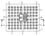
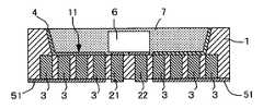
図1〜図4を参照すると、本発明に係る発光デバイスは、支持基板1と、発光素子6とを含む。発光素子6は蛍光層7によって覆われている。支持基板1は、いわゆるパッケージとなるものであって、2つの貫通電極21、22と、複数の柱状ヒートシンク3とを含み、一面に凹部11を有している。支持基板1の好ましい例は、Siを主成分とするものである。これとは異なって、支持基板1は、絶縁樹脂基板又は絶縁性セラミック基板で構成してもよい。支持基板1は、図示では、4角形状の外形を有するが、その形状は任意である。支持基板1の凹部11は、貫通電極21、22を、間隔をおいて囲むように形成されていて、その内側面のほぼ全周に、例えば、Al膜、Ag膜又はCr膜等でなる反射膜4がスパッタ等によって形成されている。反射膜4の下側には酸化膜等の絶縁膜を設けられることがある。 1 to 4, the light emitting device according to the present invention includes a
貫通電極21、22のそれぞれは、凹部11を形成した領域内において、支持基板1を厚み方向に貫通し、一端が凹部11の内面に露出し、他端が支持基板1の他面に露出する。貫通電極21、22は、中身の詰まった中実柱状体であって、角形状、円形状等、任意の断面形状をとることができる。貫通電極21、22は、支持基板1を貫通する部分と、支持基板1の一面にあって、発光素子6と接合される部分との間で、その平面形状を異ならせてもよい。例えば、支持基板1を貫通する部分の断面形状を、角形状又は円形状等の形状とし、発光素子6と接合される部分を平面積の拡大されたパターンとするなどである。また、貫通電極21,22は、その端面形状を、接続される発光素子6の電極形状と対応させることが好ましい。このような観点から、実施例では、貫通電極21の端面形状を、円形状とし、貫通電極22は、端面形状が四角形状である。 Each of the through
貫通電極21、22は、好ましくは、溶融凝固金属体でなる。溶融凝固金属体を用いることの利点は、支持基板1に設けられた縦孔内に溶融金属を流し込み、凝固させる溶融金属充填法を適用できることである。溶融金属充填法は、特許第4278007号公報に開示されている。この溶融金属充填法を適用することにより、縦孔内に流し込まれた溶融金属に、機械的な力、例えばプレス板を用いたプレス圧、射出圧または転圧を印加しながら、冷却し、凝固させ、それによって、巣、空隙、空洞のない緻密な構造を持つ貫通電極21、22を、短時間で、効率よく形成することができる。 The through
柱状ヒートシンク3は、支持基板1の厚み方向に設けられ、所定の占有率をもって分布している。柱状ヒートシンク3に適した材料は、熱抵抗の低い材料である。柱状ヒートシンク3も、貫通電極21、22と同様に、溶融凝固金属体で構成することができる。もっとも、柱状ヒートシンク3は、熱抵抗ができるだけ小さいこと好ましいから、材料及び組成比等は、そのような視点から選定する必要がある。図示実施例では、柱状ヒートシンク3は、中身の詰まった中実柱状体であって、断面円形状であるが、角形状であってもよい。 The
柱状ヒートシンク3は、その両端が支持基板1の厚み方向に貫通し、互いに微小間隔を隔てて、マトリクス状に多数配置されている。柱状ヒートシンク3は、図において、貫通電極21の側に属する一群と、貫通電極22の側に属する一群とに分かれている。貫通電極21の側に属する一群は、支持基板1の裏面(他面)に設けられた放熱体51によって共通に接続され、貫通電極22の側に属する他の一群は、支持基板1の裏面に設けられた別の放熱体52によって共通に接続されている。貫通電極21、22のリード電極は、放熱体51、52から独立させてある。この構造によれば、貫通電極21,22及び凹部11の周りには、柱状ヒートシンク3の群による放熱路を形成し、発光素子6及び貫通電極21,22からの熱を、柱状ヒートシンク3の群によって集め、その熱を、支持基板1の厚み方向に伝達し、支持基板1の他面に設けられた放熱体51、52から、支持基板1の面に沿って外部に拡散し、放出することができる。即ち、3次元的放熱経路が構成される。このため、放熱特性が向上する。A large number of
しかも、この放熱体51、52は、支持基板1に付着されたものであるから、外部放熱器を設ける場合と異なって、柱状ヒートシンク3との間に良好な熱結合構造を確立することができる。もし、柱状ヒートシンク3の端部を、放熱体51,52に共通に接続せずに、独立させたとすれば、外部放熱器に熱結合させなければならない。この場合、柱状ヒートシンク3の端部位置を、正確に同一面に位置させることは困難であるから、柱状ヒートシンク3の外部放熱器に対する熱結合が、柱状ヒートシンク3毎に異なってしまい、結果的に放熱特性が悪化する。Moreover, since the
放熱体51、52の形態は、図示の膜状に限らず、拡大された放熱面積を有する3次元的構造であってもよい。例えば、図1〜図3に示したように、貫通電極21,22及び発光素子配置領域となる凹部11を、その全周から取り囲むように配置された柱状ヒートシンク3の群において、図4に示すように、その一端の全てが、支持基板1の裏面(他面)に設けられた放熱体51によって共通に接続されていてもよい。この構造によれば、図1〜図3に示した実施の形態と同様の優れた放熱特性を確保することができる。 The form of the
柱状ヒートシンク3の奏する放熱特性は、基本的には、その組成材料の持つ熱伝導率(又は熱抵抗)と、支持基板1の平面積に対して、柱状ヒートシンク3の全体が占める占有率とによって定まる。例えば、柱状ヒートシンク3として、熱抵抗の低い材料を用いた場合には、占有率を低下させ、熱抵抗の高い材料を用いた場合には、占有率を上げる。即ち、柱状ヒートシンク3の占有率は、その組成材料の熱伝導率を考慮して定めることになる。逆に、占有率に制限がある場合には、求められる放熱特性を考慮して、適合する熱伝導率の材料を選択することになる。 The heat dissipation characteristics of the
好ましくは、貫通電極21、22及び柱状ヒートシンク3の少なくとも一方は、nmサイズの炭素原子構造体を含有するナノコンポジット構造を有し、支持基板1に設けられたビアを鋳型とする鋳込み成形体でなる。 Preferably, at least one of the through
上記炭素原子構造体は、ダイヤモンド、フラーレンまたはカーボンナノチューブから選択された少なくとも一種を含有するものである。ここでは、カーボンナノチューブを用いた場合を例にとって説明する。周知のように、カーボンナノチューブは、炭素によって作られる六員環ネットワーク(グラフェンシート)が単層あるいは多層の同軸管状になった物質である。単層のシングルウォールナノチューブ (SWNT)、多層のマルチウォールナノチューブ (MWNT) の何れを用いてもよい。 The carbon atom structure contains at least one selected from diamond, fullerene or carbon nanotube. Here, a case where carbon nanotubes are used will be described as an example. As is well known, a carbon nanotube is a substance in which a six-membered ring network (graphene sheet) made of carbon is formed into a single-layer or multilayer coaxial tube. Either single-wall single-wall nanotubes (SWNT) or multi-wall multi-wall nanotubes (MWNT) may be used.
カーボンナノチューブは、銅の10倍もの高熱伝導特性を有し、極めて高い放熱特性が得られるから、放熱特性に優れた柱状ヒートシンク3を構成することができる。これにより、発光素子6に対する許容電流値を増大させ、その発光量を増大させながら、発光素子6の異常発熱、熱暴走等を回避することができる。 Since the carbon nanotube has a heat conduction characteristic 10 times as high as that of copper and an extremely high heat dissipation characteristic can be obtained, the
また、カーボンナノチューブは、電流密度耐性が、109A/cm2で、銅の1,000倍以上の高電流密度耐性を有する。しかも、カーボンナノチューブ内では、電気良導体である銅との対比において、電子散乱が少ないため、電気抵抗が小さい。したがって、nmサイズのカーボンナノチューブを含有する貫通電極21、22によれば、銅との対比において、電気抵抗が小さく、大きな電流を流しても、抵抗発熱量を低減することができる。カーボンナノチューブは、数nmの直径であり、本発明では、これを、500nm以下、好ましくは、200nm〜300nmの長さに切断して用いる。The carbon nanotube has a current density resistance of 109 A / cm2 and a high current density resistance of 1,000 times or more that of copper. In addition, in the carbon nanotube, since the electron scattering is small in comparison with copper, which is a good electrical conductor, the electrical resistance is small. Therefore, according to the through
貫通電極21、22及び柱状ヒートシンク3は、カーボンナノチューブ自体によって構成してもよいし、カーボンナノチューブと、ナノコンポジット結晶構造の金属/合金成分を含む複合材料によって構成してもよい。nmサイズのカーボンナノチューブ及びナノコンポジット結晶構造の金属/合金成分を含むナノコンポジット構造の貫通電極21、22及び柱状ヒートシンク3は、大きさが、ナノレベルに制限された組織、結晶を含むから、その効果として、貫通電極21、22及び柱状ヒートシンク3に発生する応力が小さくなる。しかも、ナノコンポジット結晶構造には、等軸晶化を促進する働きがある。上述したナノコンポジット構造及びナノコンポジット結晶構造の有する特有の特性により、特に、半導体支持基板において、半導体回路の特性劣化が抑制される。また、支持基板1に亀裂・クラックが入るのを抑制することもできる。The through
貫通電極21、22において、ナノコンポジット結晶構造の金属/合金成分としては、Bi、In、Sn及びCuを例示することができる。特に、Biを含有させると、Biの持つ凝固時の体積膨張特性により、ビアの内部で、空洞や空隙を生じることのない緻密な貫通電極21、22を形成することができる。もっとも、Bi等を含有させると、電気抵抗が増大する傾向にあるので、要求される電気抵抗値を満たす限度で、Biを使用することが好ましい。 In the through
柱状ヒートシンク3を構成するナノコンポジット結晶構造材料の具体例としては、限定するものではないが、Al、Au、Cu、Ag、Sn等を例示することができる。もっとも、柱状ヒートシンク3は、熱抵抗ができるだけ小さいこと好ましいから、材料及び組成比等は、そのような視点から選定する必要がある。図示実施例では、柱状ヒートシンク3は、中身の詰まった柱状体であって、断面円形状であるが、角形状であってもよい。 Specific examples of the nanocomposite crystal structure material constituting the
貫通電極21、22及び柱状ヒートシンク3を形成する技術として、ビアの側面にメッキを施した上で、サーマルビアを形成するとすれば、連続しためっき膜を形成ためには、ビアの内壁面を、凹凸の極めて小さい平滑な面にしなければならず、ビア形成工程に長時間を費やさなければならなくなる。しかも、ビアのアスペクト比が高くなれば、めっきのための下地膜を連続する均質な膜として形成することが、極めて困難になる。 As a technique for forming the through
これに対して、柱状ヒートシンク3を、支持基板1に設けられたビアを鋳型とする鋳込み成形体として構成する本発明では、ビアの内壁面(側壁面)が凹凸面となっていても、柱状ヒートシンク3は、鋳込みの過程で、その凹凸面を倣うように充填されてゆく。したがって、巣、空隙、空洞のない緻密な構造を持ち、ビアの側壁面に密着した構造の柱状ヒートシンク3が得られる。よって、熱伝導性及び放熱特性に優れた柱状ヒートシンク3が実現される。 On the other hand, in the present invention in which the
しかも、ビアの内壁面の凹凸が一種のアンカー効果を生じるので、柱状ヒートシンク3がビアから浮き上がったり、あるは浮動したりすることなく、ビアの内部に確実に固定される。これは、裏返せば、従来技術との対比において、ビアの形成に当たって、その内壁面の平面度に気を使わずに済み、却って、ビアをある程度ラフに形成した方がよい結果を生むということでもある。 In addition, the irregularities on the inner wall surface of the via cause a kind of anchor effect, so that the
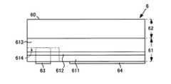
発光素子6は、発光ダイオードであって、図5、図6に例示するものは、透明結晶層62の光出射面60とは反対側の他面に、P型半導体層611及びN型半導体層613を積層した半導体積層構造61を含んでいる。P型半導体層611及びN型半導体層613の間には活性層612が設けられる。 The light-emitting
P型半導体層611及びN型半導体層613のうち、透明結晶層62の側に位置するN型半導体層613は、P型半導体層611と重ならない部分614を有しており、N側電極63が、その重ならない部分614の表面に設けられている。P側電極64は、重なる部分において、P型半導体層611の表面に設けられている。N側電極63は、円形状に限らず、角形状であってもよい。 Of the P-
実施例において、重ならない部分614に設けられたN側電極63の平面積は、重なる部分に設けられたP側電極64の平面積よりも小さい。より詳しくは、N側電極63及びP側電極64の配置方向で見た電極幅について、N側電極63の電極幅がP側電極64の電極幅よりも小さい。このような電極配置によれば、重ならない部分614の幅を小さくし、反射的に、発光領域となる重なる部分の幅及び面積を拡大できるから、発光量を増大することができる。 In the embodiment, the plane area of the N-
もっとも、図5、図6は、本発明において適用可能な発光素子6の一例を示すものであって、これに限定されるものではない。例えば、透明結晶層62と半導体積層構造61との上下関係が逆転した構造であってもよい。また、電極面積は電流拡散を考慮して定めだれる。 However, FIG. 5 and FIG. 6 show an example of the
更に、発光量増大のためには、重ならない部分614の面積は、できるだけ小さくすることが好ましい。例えば、図7及び図8に示すように、重ならない部分614が、電極63を、3方または4方から取り囲むような小面積に形成してもよい。 Furthermore, in order to increase the light emission amount, it is preferable to reduce the area of the
この発光素子6は、図1に示したように、支持基板1の凹部11内に配置され、P型半導体層611のP側電極64が、貫通電極22の一端に接続され、N型半導体層613のN側電極63が、貫通電極21の一端に接続されている。発光素子6は、凹部11の内部に配置されたとき、その上面が凹部11の周りの支持基板1の表面よりも、低くなるように配置される。そして、その段差を埋めるように、蛍光層7を充填してある。 As shown in FIG. 1, the
P側電極64及びN側電極63は、間隔を隔てて互いに対向している。P側電極64と貫通電極22との接合、及び、N側電極63と貫通電極21との接合にあたっては、両者の接合界面に接合膜を介在させる。接合膜は、Sn、In、Bi、Ga又はSbの群から選択された少なくても1種の低融点金属成分と、Cr、Ag、Cu、Au、Pt、Pd、Ni、Ni−P合金、Ni−B合金の群から選択された少なくとも1種を含む高融点金属材料からなる。低融点金属は、P側電極64及び貫通電極22、N側電極63及び貫通電極21と反応して、金属間化合物を形成して消費され、接合後は融点が大幅に上昇する。透明結晶層62は、代表的にはサファイアであり、その一面が光出射面60となる。透明結晶層62の一面上には、バッファ層(図示しない)があり、半導体積層構造61は、バッファ層を介して、透明結晶層62の上に成長させてある。 The P-
半導体積層構造61は、発光素子6において周知である。PN接合を持ち、代表的にはIII−V族化合物半導体が用いられる。もっとも、公知技術に限らず、これから提案されることのある化合物半導体を含むことができる。 The semiconductor stacked
本発明において、発光素子6は、赤色発光素子、緑色発光素子、青色発光素子、橙色発光素子の何れであってもよいし、白色発光素子であってもよい。それらの発光素子において、半導体積層構造61を構成する半導体材料及びその製造方法は既に知られている。
上述したように、本発明に係る発光デバイスは、支持基板1を含んでおり、この支持基板1は、複数の柱状ヒートシンク3を含んでいる。柱状ヒートシンク3は、支持基板1の厚み方向に設けられている。したがって、発光素子6の発光動作によって生じた熱を、柱状ヒートシンク3によって、支持基板1の外部に放熱し、発光素子6の電極63、64と貫通電極21、22とを接続する接合部分の接合強度を保存し、電気的接続の信頼性を維持することができる。また、発熱による発光素子6の発光特性の変動を回避することができる。In the present invention, the
As described above, the light emitting device according to the present invention includes the
本発明に係る発光デバイスにおいて、支持基板1は、2つの貫通電極21、22を含み、一面に凹部11を有している。貫通電極21、22のそれぞれは、支持基板1を厚み方向に貫通し、一端が凹部11の内面に露出している。この支持基板1の凹部11内に発光素子6が配置されている。発光素子6は、実施例では、透明結晶層62の光出射面となる一面60とは反対側の他面に、P型半導体層611及びN型半導体層613を積層した構造である。そして、凹部11の内部で、P型半導体層611のP側電極64が貫通電極22の一端に接続され、N型半導体層613のN側電極63が、貫通電極21、22の他方の一端に接続されている。したがって、実施例によれば、発光素子6に対しては、透明結晶層62のある側とは反対側から、電流が注入されることになり、発光素子6のための電極が、光出射面60に現れない構造が実現されることになる。よって、発生した光を、効率よく外部に放射させ得る。 In the light emitting device according to the present invention, the
実施例では、凹部11の内面と発光素子6の側面との間に、反射膜4が設けられている。これにより、半導体層61で生じた光を、透明結晶層62における光散乱・吸収作用を抑えながら、透明結晶層62の光出射面60に導くことができる。
反射膜4は、凹部11の内面に付着されていてもよいし、発光素子6の側面に付着されていてもよい。図1〜図3の実施例では、発光素子6は、凹部11に対して、微小なクリアランスを有して、嵌めこまれている。この構造によれば、支持基板1に対する発光素子6の位置決め・配置を、容易、かつ、確実に実行することができる。In the embodiment, the
The
図示はされていないが、光出射面60に、微細凹凸形状を有する透明光学部品を配置することができる。これにより、光出射面60で、光を拡散又は分散させ、均一な面発光を実現することができる。透明光学部品を設ける代わりに、光出射面60に、微細凹凸形状が形成されていてもよい。さらに、図示は省略するけれども、微細凹凸とともに、あるいは、微細凹凸を設けることなく、光出射面60に蛍光体を設けてもよい。 Although not shown, a transparent optical component having a fine uneven shape can be disposed on the
さらに、図9を参照すると、支持基板1に、図1〜図3の実施の形態との対比において、凹部11の平面積を拡大した発光デバイスが図示されている。この凹部11は、発光素子6の平面積よりもかなり大きく、発光素子6の外周と、凹部11の内周面との間に蛍光層7等が充填されている。また、凹部11の内壁面に反射膜4が付着されている。柱状ヒートシンク3は、一端(上端)が凹部11の底面位置と略同じ位置で止まっていて、他端が支持基板1の裏面に導かれ、放熱体51に接続されている。
図10を参照すると、図9と略同じような構造において、凹部11の中央部分に、突出部12を設け、この突出部12に発光素子6を搭載した発光デバイスが図示されている。
図9及び図10の実施の形態も、図1〜図6を参照して説明した作用効果を奏する。Further, referring to FIG. 9, a light emitting device in which the plane area of the
Referring to FIG. 10, there is illustrated a light emitting device in which a
The embodiment of FIGS. 9 and 10 also has the effects described with reference to FIGS.
本発明に係る発光デバイスは、単一の発光素子である発光ダイオード、複数の発光素子を、例えばマトリクス状に配置した面発光装置、照明装置、液晶ディスプレイ用バックライト、信号灯等、広範な用途を持っている。 The light-emitting device according to the present invention has a wide range of uses such as a light-emitting diode that is a single light-emitting element, a surface light-emitting device in which a plurality of light-emitting elements are arranged in a matrix, a lighting device, a backlight for a liquid crystal display, a signal lamp, and the like. have.
以上、好ましい実施例を参照して本発明の内容を具体的に説明したが、本発明の基本的技術思想及び教示に基づいて、当業者であれば、種種の変形態様を採り得ることは自明である。 Although the contents of the present invention have been specifically described above with reference to the preferred embodiments, it is obvious that those skilled in the art can take various modifications based on the basic technical idea and teachings of the present invention. It is.
1 支持基板
21 貫通電極
22 貫通電極
3 柱状ヒートシンク
4 反射膜DESCRIPTION OF
Claims (1)
Translated fromJapanese前記支持基板は、2つの貫通電極と、複数の柱状ヒートシンクとを含み、一面に発光素子配置領域を有しており、
前記貫通電極のそれぞれは、前記支持基板を厚み方向に貫通し、一端が前記発光素子配置領域の面内に露出しており、
前記発光素子は、P型半導体層及びN型半導体層を積層した構造を含み、前記支持基板の凹部内に配置され、前記P型半導体層のP側電極が、前記貫通電極の一方の前記一端に接続され、前記N型半導体層のN側電極が、前記貫通電極の他方の前記一端に接続されており、
前記柱状ヒートシンクは、前記支持基板の厚み方向に設けられ、前記発光素子配置領域を取り囲んで、その周りに互いに間隔をおいて配置され、それぞれの一端が、前記支持基板の他面に付着して一体に設けられた放熱体に共通に接続されており、
前記貫通電極及び前記柱状ヒートシンクは、nmサイズの炭素原子構造体及びナノコンポジット結晶構造の金属成分又は合金成分を含有するナノコンポジット構造を有し、前記基板に設けられたビアを鋳型とする鋳込み成形体でなる、
発光デバイス。
A light emitting device including a support substrate and a light emitting element,
The support substrate includes two through electrodes and a plurality of columnar heat sinks, and has a light emitting element arrangement region on one surface,
Each of the through electrodes penetrates the support substrate in the thickness direction, and one end is exposed in the plane of the light emitting element arrangement region.
The light-emitting element includes a structure in which a P-type semiconductor layer and an N-type semiconductor layer are stacked, and is disposed in arecess of the support substrate, and the P-side electrode of the P-type semiconductor layer is one end of the through electrode. N-side electrode of the N-type semiconductor layer is connected to the other end of the through electrode,
The columnar heat sink is provided in the thickness direction of the support substrate, surrounds the light emitting element arrangement region, and is disposed around the light emitting element arrangement region, with one end attached to the other surface of the support substrate. It is connected in common to the heat radiator provided integrally,
The through electrode and the columnar heat sink have a nanocomposite structure containing a metal component or alloy component of nm-size carbon atom structure and nanocomposite crystal structure, and casting is performed using a via provided in the substrate as a mold The body,
Light emitting device.
Priority Applications (1)
| Application Number | Priority Date | Filing Date | Title |
|---|---|---|---|
| JP2011223050AJP5709718B2 (en) | 2011-01-04 | 2011-10-07 | Light emitting device |
Applications Claiming Priority (3)
| Application Number | Priority Date | Filing Date | Title |
|---|---|---|---|
| JP2011000241 | 2011-01-04 | ||
| JP2011000241 | 2011-01-04 | ||
| JP2011223050AJP5709718B2 (en) | 2011-01-04 | 2011-10-07 | Light emitting device |
Publications (3)
| Publication Number | Publication Date |
|---|---|
| JP2012156484A JP2012156484A (en) | 2012-08-16 |
| JP2012156484A5 JP2012156484A5 (en) | 2013-07-25 |
| JP5709718B2true JP5709718B2 (en) | 2015-04-30 |
Family
ID=46837856
Family Applications (1)
| Application Number | Title | Priority Date | Filing Date |
|---|---|---|---|
| JP2011223050AActiveJP5709718B2 (en) | 2011-01-04 | 2011-10-07 | Light emitting device |
Country Status (1)
| Country | Link |
|---|---|
| JP (1) | JP5709718B2 (en) |
Families Citing this family (3)
| Publication number | Priority date | Publication date | Assignee | Title |
|---|---|---|---|---|
| US10497846B2 (en)* | 2017-07-11 | 2019-12-03 | Lg Innotek Co., Ltd. | Light emitting device package |
| CN109698263B (en)* | 2018-11-28 | 2023-11-03 | 广东晶科电子股份有限公司 | Packaging substrate, semiconductor device and manufacturing method thereof |
| CN113594342B (en)* | 2021-05-19 | 2022-09-02 | 西安电子科技大学芜湖研究院 | Nano-column LED structure with nested diamond heat dissipation layer and preparation method |
Family Cites Families (11)
| Publication number | Priority date | Publication date | Assignee | Title |
|---|---|---|---|---|
| JP2005158957A (en)* | 2003-11-25 | 2005-06-16 | Matsushita Electric Works Ltd | Light emitting device |
| JP2006066412A (en)* | 2004-08-24 | 2006-03-09 | Mitsubishi Electric Corp | Semiconductor device and semiconductor device manufacturing method |
| JP2006144030A (en) | 2004-11-16 | 2006-06-08 | Bridgestone Corp | High thermal conductivity composite material and manufacturing method therefor |
| JP5209177B2 (en)* | 2005-11-14 | 2013-06-12 | 新光電気工業株式会社 | Semiconductor device and manufacturing method of semiconductor device |
| JP2008004777A (en) | 2006-06-22 | 2008-01-10 | Nfk Lite Mfg Co Ltd | Manufacturing method for light-emitting diode excellent in heat-dissipation effect |
| JP2008155489A (en) | 2006-12-25 | 2008-07-10 | Namiki Precision Jewel Co Ltd | Carbon fiber joined body and article using the same |
| JP2007194630A (en) | 2007-01-15 | 2007-08-02 | Furukawa Electric Co Ltd:The | Solder joint layer |
| JP2008294253A (en)* | 2007-05-25 | 2008-12-04 | Ngk Spark Plug Co Ltd | Wiring board for packaging light emitting element |
| JP5315688B2 (en)* | 2007-12-28 | 2013-10-16 | 株式会社ニコン | Multilayer semiconductor device |
| JP2010238941A (en)* | 2009-03-31 | 2010-10-21 | Sanyo Electric Co Ltd | Light emitting device |
| JP4505545B1 (en)* | 2009-11-30 | 2010-07-21 | 有限会社ナプラ | Circuit board and electronic device |
- 2011
- 2011-10-07JPJP2011223050Apatent/JP5709718B2/enactiveActive
Also Published As
| Publication number | Publication date |
|---|---|
| JP2012156484A (en) | 2012-08-16 |
Similar Documents
| Publication | Publication Date | Title |
|---|---|---|
| JP5250707B2 (en) | Electronic equipment substrate and electronic equipment | |
| CN102593100A (en) | Substrate for electronic device and electronic device | |
| JP5564129B2 (en) | Light emitting device in a magnetic field | |
| JP4001169B2 (en) | Semiconductor device | |
| TWI721302B (en) | Light emitting device | |
| JP4778107B1 (en) | Light emitting device and manufacturing method thereof | |
| JP5356972B2 (en) | Heat dissipating component, manufacturing method thereof, and semiconductor package | |
| JP5124688B2 (en) | Lighting device, display, and signal lamp | |
| US7878232B2 (en) | Light emitting chip apparatuses with a thermally superconducting heat transfer medium for thermal management | |
| JP2010526425A (en) | Semiconductor light emitting device, and light source device and illumination system using the same | |
| JP4009208B2 (en) | Light emitting device | |
| JP2007142479A (en) | Semiconductor device | |
| JP5709719B2 (en) | Electronic component support apparatus and electronic device | |
| JP5709718B2 (en) | Light emitting device | |
| CN102194972A (en) | Light emitting device packaging components | |
| JP4833827B2 (en) | Anisotropic cooling element, Peltier module including the same, light emitting diode element, semiconductor laser element | |
| JP4927571B2 (en) | Semiconductor element, semiconductor module and electronic device | |
| JP2011176060A (en) | Light-emitting device | |
| JP2007305977A (en) | Semiconductor laser device and manufacturing method thereof | |
| JP2007173874A (en) | Light emitting device | |
| JP6569217B2 (en) | Light emitting device | |
| US10825974B2 (en) | Light-emitting diode package and method of manufacture | |
| JP2023089984A (en) | Light-emitting device | |
| KR101118032B1 (en) | A Cooling Structure For LED Chip | |
| JP2011082264A (en) | Led package |
Legal Events
| Date | Code | Title | Description |
|---|---|---|---|
| A521 | Request for written amendment filed | Free format text:JAPANESE INTERMEDIATE CODE: A523 Effective date:20130610 | |
| A621 | Written request for application examination | Free format text:JAPANESE INTERMEDIATE CODE: A621 Effective date:20130610 | |
| A871 | Explanation of circumstances concerning accelerated examination | Free format text:JAPANESE INTERMEDIATE CODE: A871 Effective date:20130610 | |
| A975 | Report on accelerated examination | Free format text:JAPANESE INTERMEDIATE CODE: A971005 Effective date:20130625 | |
| A131 | Notification of reasons for refusal | Free format text:JAPANESE INTERMEDIATE CODE: A131 Effective date:20130703 | |
| A521 | Request for written amendment filed | Free format text:JAPANESE INTERMEDIATE CODE: A523 Effective date:20130830 | |
| A131 | Notification of reasons for refusal | Free format text:JAPANESE INTERMEDIATE CODE: A131 Effective date:20131030 | |
| A521 | Request for written amendment filed | Free format text:JAPANESE INTERMEDIATE CODE: A523 Effective date:20131114 | |
| A02 | Decision of refusal | Free format text:JAPANESE INTERMEDIATE CODE: A02 Effective date:20140122 | |
| A521 | Request for written amendment filed | Free format text:JAPANESE INTERMEDIATE CODE: A523 Effective date:20140307 | |
| A911 | Transfer to examiner for re-examination before appeal (zenchi) | Free format text:JAPANESE INTERMEDIATE CODE: A911 Effective date:20140324 | |
| A912 | Re-examination (zenchi) completed and case transferred to appeal board | Free format text:JAPANESE INTERMEDIATE CODE: A912 Effective date:20140425 | |
| A521 | Request for written amendment filed | Free format text:JAPANESE INTERMEDIATE CODE: A523 Effective date:20141225 | |
| A61 | First payment of annual fees (during grant procedure) | Free format text:JAPANESE INTERMEDIATE CODE: A61 Effective date:20150303 | |
| R150 | Certificate of patent or registration of utility model | Ref document number:5709718 Country of ref document:JP Free format text:JAPANESE INTERMEDIATE CODE: R150 | |
| R250 | Receipt of annual fees | Free format text:JAPANESE INTERMEDIATE CODE: R250 | |
| R250 | Receipt of annual fees | Free format text:JAPANESE INTERMEDIATE CODE: R250 | |
| R250 | Receipt of annual fees | Free format text:JAPANESE INTERMEDIATE CODE: R250 | |
| R250 | Receipt of annual fees | Free format text:JAPANESE INTERMEDIATE CODE: R250 | |
| R250 | Receipt of annual fees | Free format text:JAPANESE INTERMEDIATE CODE: R250 | |
| R250 | Receipt of annual fees | Free format text:JAPANESE INTERMEDIATE CODE: R250 | |
| R250 | Receipt of annual fees | Free format text:JAPANESE INTERMEDIATE CODE: R250 |