JP5705683B2 - Tunnel magnetoresistive element, non-local spin injection element, and magnetic head using the same - Google Patents
Tunnel magnetoresistive element, non-local spin injection element, and magnetic head using the sameDownload PDFInfo
- Publication number
- JP5705683B2 JP5705683B2JP2011180588AJP2011180588AJP5705683B2JP 5705683 B2JP5705683 B2JP 5705683B2JP 2011180588 AJP2011180588 AJP 2011180588AJP 2011180588 AJP2011180588 AJP 2011180588AJP 5705683 B2JP5705683 B2JP 5705683B2
- Authority
- JP
- Japan
- Prior art keywords
- film
- ferromagnetic
- lattice
- seed
- barrier
- Prior art date
- Legal status (The legal status is an assumption and is not a legal conclusion. Google has not performed a legal analysis and makes no representation as to the accuracy of the status listed.)
- Expired - Fee Related
Links
Images


Landscapes
- Mram Or Spin Memory Techniques (AREA)
- Magnetic Heads (AREA)
- Hall/Mr Elements (AREA)
Description
Translated fromJapanese本発明は、トンネル磁気抵抗効果素子、非局所スピン注入素子、及びそれを用いた磁気ヘッドに関するものである。 The present invention relates to a tunnel magnetoresistive effect element, a non-local spin injection element, and a magnetic head using the same.
非磁性障壁膜を介したスピン注入素子は、強磁性固定膜の上に非磁性障壁膜を積層した構造を有し、磁気ヘッドや不揮発メモリ等に使われるトンネル磁気抵抗効果素子(例えば非特許文献1)や、磁気ヘッド等に応用可能な純粋スピン流を生じさせる非局所スピン注入素子(例えば非特許文献2)等に使われる。 A spin injection device via a nonmagnetic barrier film has a structure in which a nonmagnetic barrier film is laminated on a ferromagnetic pinned film, and is a tunnel magnetoresistive effect element used for a magnetic head, a nonvolatile memory, or the like (for example, non-patent literature) 1), and a non-local spin injection device (for example, Non-Patent Document 2) that generates a pure spin current applicable to a magnetic head or the like.
スピン注入素子としては、非特許文献1に記載されたような、AlOxを障壁膜として用い、その障壁膜を二つの強磁性膜で挟んだトンネル磁気抵抗効果素子が知られているが、このトンネル磁気抵抗効果素子では工業的に使用するための十分な電気的出力信号を得ることができなかった。As a spin injection element, a tunnel magnetoresistive element using AlOx as a barrier film and sandwiching the barrier film between two ferromagnetic films, as described in
最近、スピン注入素子の障壁膜としてMgOを用いることにより、上記したAlOxを障壁膜に用いたスピン注入素子よりも高効率なスピン注入が実現され、結果としてトンネル磁気抵抗効果素子において室温で604%に達する大きな磁気抵抗比が得られることが報告されている(例えば非特許文献3,4)。MgOを非磁性障壁膜に用いることで高いスピン注入効率を実現するのは、MgOが岩塩構造の(001)方向に配向するためだと言われている(例えば非特許文献5,6)。Recently, by using MgO as the barrier film of the spin injection element, spin injection with higher efficiency than that of the above-described spin injection element using AlOx as the barrier film has been realized. As a result, the tunnel magnetoresistive effect element has 604 at room temperature. It has been reported that a large magnetoresistive ratio reaching% can be obtained (for example,
化学式Mg1-aXaO(XはZn,Cd,Ca,Sr,及びBaの内から選んだ一種又は二種以上、0<a≦1)で表される酸化物は、MgOよりもバンドギャップが小さく、スピン注入素子の低抵抗化が期待できる。また、Xの分量がある程度以下であれば岩塩構造を保つことが知られており(例えば非特許文献7)、上記の酸化物を用いた磁気抵抗効果素子は例えば特許文献1に開示されている。An oxide represented by the chemical formula Mg1-a Xa O (X is one or more selected from Zn, Cd, Ca, Sr, and Ba, 0 <a ≦ 1) is a band more than MgO. The gap is small and the resistance of the spin injection device can be reduced. Further, it is known that a rock salt structure is maintained if the amount of X is a certain amount or less (for example, Non-Patent Document 7), and a magnetoresistive element using the above oxide is disclosed in, for example,
ハードディスクの磁気ヘッドや不揮発性磁気メモリに応用可能なスピン注入素子は最近注目を集めているが、必須の構造である障壁膜には酸化物からなる絶縁体が使われており、素子自体の高い抵抗が微細化したデバイス開発の障害となっている。そのため、低抵抗かつ高効率なスピン注入を実現する素子の開発が求められているが、MgOよりも高いスピン注入効率を有する障壁膜は今のところ見つかっていない。そのため酸化物を用いながらも、低抵抗かつ高効率なスピン注入を実現する障壁膜の開発が強く要望されている。 Spin injection devices applicable to hard disk magnetic heads and non-volatile magnetic memories have recently attracted attention, but the barrier film, which is an essential structure, uses an insulator made of oxide, and the device itself is high. This is an obstacle to the development of miniaturized devices. Therefore, development of a device that realizes low resistance and high efficiency spin injection is required, but no barrier film having higher spin injection efficiency than MgO has been found so far. Therefore, there is a strong demand for the development of a barrier film that realizes low-resistance and high-efficiency spin injection while using an oxide.
スピン注入素子の障壁膜としてMgOを使用した場合、膜厚を規定すると酸化マグネシウム固有のバンドギャップで素子の抵抗が決まってしまうため、素子の低抵抗化は困難である。そこで、MgOよりもバンドギャップが小さく、かつ大きなスピン注入効率を有する障壁膜の開発が強く望まれている。 When MgO is used as the barrier film of the spin injection element, if the film thickness is defined, the resistance of the element is determined by the band gap unique to magnesium oxide, so it is difficult to reduce the resistance of the element. Therefore, development of a barrier film having a smaller band gap and higher spin injection efficiency than MgO is strongly desired.
本発明は、小さいバンドギャップを持つ障壁膜を岩塩構造の(001)方向に高配向させて、上記の要請に有利に応えることのできる低抵抗かつ高効率なスピン注入素子を提供することを目的とする。 An object of the present invention is to provide a low-resistance and high-efficiency spin injection device that can advantageously meet the above requirements by highly orienting a barrier film having a small band gap in the (001) direction of a rock salt structure. And
スピン注入素子において高いスピン注入効率を達成するためには、完全にスピン分極したΔ1バンドの電子を選択的に透過させる必要があり、障壁膜は岩塩構造の(001)方向に配向していることが望ましい。しかし、上記酸化物Mg1-aXaOはMgOよりも岩塩構造(001)配向の配向性が悪く、低抵抗化も高いスピン注入効率も実現できないことがわかった。この結晶配向の不安定性はMgOに異種酸化物を混合したことにより岩塩構造が不安定化したためと考えられる。In order to achieve high spin injection efficiency in the spin injection device, it is necessary to selectively transmit completely spin-polarized Δ1 band electrons, and the barrier film is oriented in the (001) direction of the rock salt structure. It is desirable. However, it has been found that the above-mentioned oxide Mg1-a Xa O has a lower rock salt (001) orientation than MgO, and cannot achieve low resistance and high spin injection efficiency. This instability of crystal orientation is thought to be due to the rock salt structure being destabilized by mixing different oxides with MgO.
その一方で、ウルツ鋼構造のZnOに圧力を印加して格子を縮めると岩塩構造に転移すること(J. E. Jaffe et al., Phys. Rev. B 48 7903 (1993))や、Mg1-aZnaOにおいて同じZnの組成割合であれば格子定数が小さいほど岩塩構造が安定なこと(I. V. Maznichenko et al., Phys. Rev. B 80, 144101 (2009))が知られている。つまり、小さなバンドギャップを持つ酸化物Mg1-aXaOの格子定数を小さくすることにより、酸化物Mg1-aXaOの岩塩構造(001)方向の配向性が高められると考えられる。On the other hand, when the lattice is shrunk by applying pressure to ZnO in the Wurtz steel structure, it changes to a rock salt structure (JE Jaffe et al., Phys. Rev. B 48 7903 (1993)), and Mg1-a Zn it rock salt structure as the lattice constant is small it is stable if the composition ratio of the same Zn ina O (IV Maznichenko et al. , Phys. Rev. B 80, 144101 (2009)) are known. That is, it is considered that by reducing the lattice constant of the oxide Mg1-a Xa O having a small band gap, the orientation of the oxide Mg1-a Xa O in the rock salt structure (001) direction is enhanced. .
ここで、障壁膜の格子定数を小さくするには、障壁膜よりも格子定数の小さなシード膜を障壁膜の下に配置することが考えられる。しかし、MgO等の酸化物や強磁性膜をシード膜に用いると、現時点でかなり最適化されている、前出のΔ1バンドを選択的に透過させるための構造設計が難しくなってしまう。また、絶縁体をシード膜として用いると障壁膜とあわせた総膜厚が大きくなることにより抵抗が大幅に増加してしまい、低抵抗化が達成できない。そこで発明者らは、障壁膜の格子定数を小さくする非磁性シード膜を強磁性膜の下に配置し、障壁膜の岩塩構造の配向性向上を補助することで、所期した目的が有利に達成される新規知見を得た。本発明は上記の知見に立脚するものである。Here, in order to reduce the lattice constant of the barrier film, a seed film having a lattice constant smaller than that of the barrier film may be disposed under the barrier film. However, when an oxide such as MgO or a ferromagnetic film is used as a seed film, it becomes difficult to design a structure for selectively transmitting the above-described Δ1 band, which is considerably optimized at the present time. In addition, when an insulator is used as a seed film, the total film thickness including the barrier film is increased, so that the resistance is significantly increased, and a reduction in resistance cannot be achieved. Therefore, the inventors have placed the nonmagnetic seed film that reduces the lattice constant of the barrier film below the ferromagnetic film, and helps to improve the orientation of the rock salt structure of the barrier film, so that the intended purpose is advantageous. Gained new knowledge to be achieved. The present invention is based on the above findings.
本発明によるトンネル磁気抵抗効果素子は、第一の強磁性膜と、第一の強磁性膜の上に設けられた障壁膜と、障壁膜の上に設けられた第二の強磁性膜と、第一の強磁性膜の下に設けられた非磁性シード膜とを有し、第一の強磁性膜と第二の強磁性膜は(001)配向した体心立方格子の膜、障壁膜は(001)配向した岩塩構造の酸化物の膜であり、非磁性シード膜は第一の強磁性膜よりも小さな格子定数を持つ非磁性金属膜である。障壁膜はMg1-aXaO(XはZn,Cd,Ca,Sr,Ba,及びBの内から選んだ一種又は二種以上、0<a≦1)とすることができる。A tunnel magnetoresistive element according to the present invention includes a first ferromagnetic film, a barrier film provided on the first ferromagnetic film, a second ferromagnetic film provided on the barrier film, A non-magnetic seed film provided under the first ferromagnetic film, the first ferromagnetic film and the second ferromagnetic film being a (001) -oriented body-centered cubic lattice film, and the barrier film being The (001) oriented oxide film of rock salt structure, and the nonmagnetic seed film is a nonmagnetic metal film having a lattice constant smaller than that of the first ferromagnetic film. The barrier film may be Mg1-a Xa O (X is one or more selected from Zn, Cd, Ca, Sr, Ba, and B, and 0 <a ≦ 1).
本発明による非局所スピン注入素子は、強磁性膜と、強磁性膜の上に設けられた障壁膜と、障壁膜の上に設けられた非磁性導電膜と、強磁性膜の下に設けられた非磁性シード膜とを有し、強磁性膜は(001)配向した体心立方格子の膜、障壁膜は(001)配向した岩塩構造の酸化物の膜であり、非磁性シード膜は強磁性膜よりも小さな格子定数を持つ非磁性金属膜である。 A nonlocal spin injection device according to the present invention is provided under a ferromagnetic film, a barrier film provided on the ferromagnetic film, a nonmagnetic conductive film provided on the barrier film, and the ferromagnetic film. The ferromagnetic film is a (001) -oriented body-centered cubic lattice film, the barrier film is a (001) -oriented rock salt structure oxide film, and the non-magnetic seed film is a strong film. It is a nonmagnetic metal film having a lattice constant smaller than that of the magnetic film.
また、本発明による非局所スピン注入素子は、非磁性導電膜と、非磁性導電膜の上に設けられた障壁膜と、障壁膜の上に設けられた強磁性膜とを有し、強磁性膜は(001)配向した体心立方格子の膜、障壁膜は(001)配向した岩塩構造の酸化物の膜であり、非磁性導電膜は障壁膜よりも小さな格子定数を持つ非磁性金属膜である。 A nonlocal spin injection device according to the present invention includes a nonmagnetic conductive film, a barrier film provided on the nonmagnetic conductive film, and a ferromagnetic film provided on the barrier film, The film is a (001) oriented body-centered cubic lattice film, the barrier film is a (001) oriented rock salt oxide film, and the nonmagnetic conductive film is a nonmagnetic metal film having a lattice constant smaller than that of the barrier film. It is.
非局所スピン注入素子の障壁膜としては、Mg1-aXaO(XはZn,Cd,Ca,Sr,Ba,及びBの内から選んだ一種又は二種以上、0<a≦1)を用いることができる。As the barrier film of the non-local spin injection device, Mg1-a Xa O (X is one or more selected from Zn, Cd, Ca, Sr, Ba, and B, 0 <a ≦ 1) Can be used.
本発明によると、低抵抗かつ高いスピン注入効率を併せ持つスピン注入素子が得られる。従って、この新規な特性を付随させたスピン注入素子を搭載することにより、微細化に適した高出力の磁気ヘッドや低抵抗の不揮発性磁気メモリを実現することが可能になる。
上記した以外の、課題、構成及び効果は、以下の実施形態の説明により明らかにされる。According to the present invention, a spin injection device having both low resistance and high spin injection efficiency can be obtained. Therefore, by mounting a spin injection device with this new characteristic, it is possible to realize a high-output magnetic head and a low-resistance nonvolatile magnetic memory suitable for miniaturization.
Problems, configurations, and effects other than those described above will be clarified by the following description of embodiments.
以下、図面を参照して本発明の実施の形態を説明する。以下の図において、同じ構成部分には同一の符号を付し、重複する説明を省略する。 Embodiments of the present invention will be described below with reference to the drawings. In the following drawings, the same components are denoted by the same reference numerals, and redundant description is omitted.
[実施例1]
図1は、本発明によるトンネル磁気抵抗効果素子の一例を示す断面模式図である。このトンネル磁気抵抗効果素子1は、下地膜300、非磁性シード膜310、強磁性膜305、障壁膜307、強磁性膜308、保護膜309を積層して形成され、非磁性シード膜310を格子定数が強磁性膜305の格子定数の√2倍よりも小さい面心立方格子の物質を用いることにより面積抵抗と磁気抵抗比が改善される。本実施例では、トンネル磁気抵抗効果素子はマグネトロンスパッタリング法を用いて作製し、成膜後300℃で磁界中でのアニール処理を施した。[Example 1]
FIG. 1 is a schematic cross-sectional view showing an example of a tunnel magnetoresistive effect element according to the present invention. This tunnel magnetoresistive
下地膜300はTa(5nm)/Ru(10nm)/Ta(5nm)、保護膜309はTa(5nm)/Ru(5nm)により形成した。強磁性膜305は(001)配向した体心立方格子をもつFe(5nm)を、強磁性膜308には(001)配向した体心立方格子をもつFe(3nm)を用い、障壁膜307にはMgO(1.5nm)及びMgOとZnOの混晶であるMg0.7Zn0.3O(1.5nm)を用いた。MgOやMg0.7Zn0.3Oは、岩塩構造を有し、(001)配向している。非磁性シード膜310にはPd(3nm)を使用した。面心立方格子構造を持つPdの格子定数は0.389nmであり、その(001)面内格子間距離は1/√2倍の0.275nmとなるため、体心立方格子構造を持つFeの格子定数0.287nmよりも小さい。そのため、非磁性シード膜310としてPdを配置することにより、Pdの上に積層する強磁性膜305であるFeの結晶格子が縮み、さらに強磁性膜305を下地として育つ障壁膜307の格子定数も小さくなると考えられる。The
図2に、MgO(15nm)とMg0.7Zn0.3O(15nm)に対するX線回折のθ−2θ測定結果を示す。岩塩構造(002)配向に対応する2θ〜42.9°のピークはMg0.7Zn0.3Oの方がMgOよりも小さく、Mg0.7Zn0.3Oの岩塩構造(001)配向性がMgOよりも悪いことがわかる。FIG. 2 shows the results of θ-2θ measurement of X-ray diffraction with respect to MgO (15 nm) and Mg0.7 Zn0.3 O (15 nm). The peak of 2θ-42.9 ° corresponding to the rock salt structure (002) orientation is that Mg0.7 Zn0.3 O is smaller than MgO, and the rock salt structure (001) orientation of Mg0.7 Zn0.3 O is worse than MgO. I understand.
図3に、障壁膜307にMgO(1.5nm)、Mg0.7Zn0.3O(1.5nm)及びPdシードを配置したMg0.7Zn0.3O(1.5nm)を適用したトンネル磁気抵抗効果素子の面積抵抗RAと磁気抵抗効果比(TMR比)を示す。Figure 3, MgO (1.5nm) the barrier layer307, Mg 0.7 Zn 0.3 O ( 1.5nm) and Pd seed placement was Mg0.7 Zn0.3 O (1.5nm) applies the tunnel magnetoresistance effect element The area resistance RA and the magnetoresistance effect ratio (TMR ratio) are shown.
MgOを用いると面積抵抗RA〜1.15kΩμm2でTMR比〜140%であったのに対し、Mg0.7Zn0.3Oを用いるとバンドギャップはMgOよりも小さいにも関わらず、面積抵抗RA〜3.1kΩμm2と3倍近くに上昇し、かつTMR比〜70%と半分程に減少した。これはMg0.7Zn0.3Oの岩塩構造(001)配向がMgOに比べて弱く、障壁膜中での減衰率が小さいΔ1バンドの電子の選択的な透過を妨げてしまうためと考えられる。結果として、トンネル磁気抵抗効果素子のRAが上昇し、また、この完全スピン分極しているΔ1バンドの電子の透過が妨げられたことで、TMR比も減少していると考えられる。When MgO is used, the sheet resistance RA is 1.15 kΩμm2 and the TMR ratio is 140%. On the other hand, when Mg0.7 Zn0.3 O is used, the sheet resistance RA is 3 to 3 although the band gap is smaller than that of MgO. .1 kΩμm2 and increased nearly 3 times, and decreased to about TMR ratio ˜70%. This is considered to be because the rock salt structure (001) orientation of Mg0.7 Zn0.3 O is weaker than that of MgO, and the selective transmission of Δ1 band electrons having a small attenuation rate in the barrier film is hindered. As a result, the RA of the tunnel magnetoresistive effect element is increased, and the TMR ratio is also decreased because the transmission of this completely spin-polarized Δ1 band electron is prevented.
ここでMg0.7Zn0.3Oを用いた磁気抵抗効果素子において、強磁性膜305の下にPdを配置すると、RA〜0.6kΩμm2とMgOよりも大きく減少し、またTMR比〜130%とほぼMgOと同じTMR比を維持した。これはPdを配置することによりMg0.7Zn0.3Oの結晶格子が小さくなる方向に歪み、結果として岩塩構造(001)配向が安定化し、MgOと同様にΔ1バンドの電子の選択的な透過が達成されているためと考えられる。Here, in the magnetoresistive effect element using Mg0.7 Zn0.3 O, when Pd is disposed under the
障壁膜307はMg1-aXaO(XはZn,Cd,Ca,Sr,Ba,及びBの内から選んだ一種又は二種以上、0<a≦1)であってもよい。ここでXの組成割合が多い程バンドギャップは減少するが、その一方で混晶の岩塩構造はより不安定化する。そのため添加物Xに併せて、最適な組成aを選択する必要がある。The
非磁性シード膜310は、Pd,Rh,Pt,Al,Cu,Ag,Au,Ir,及びPbを少なくとも一種含んだ面心立方格子、又はNa,V,Cr,Rb,Mo,Ba,及びWを少なくとも一種含んだ体心立方格子を持つ金属であってもよい。但し、非磁性シード膜310の格子定数が強磁性膜305の格子定数に比べて極端に小さくなると、非磁性シード膜310と強磁性膜305の格子整合が保たれず、強磁性膜305の結晶格子歪みが起こらない。そのため、非磁性シード膜の格子定数は、強磁性膜305に格子整合させたときに、格子定数で数%程度小さい金属を選択する必要がある。 The
[実施例2]
図4は、本発明によるトンネル磁気抵抗効果素子の一例を示す断面模式図である。このトンネル磁気抵抗効果素子2は、下地膜300、配向制御膜301、反強磁性膜302、強磁性膜303、非磁性シード膜304、強磁性膜305、絶縁シード膜306、障壁膜307、強磁性膜308、保護膜309を積層して形成されている。非磁性シード膜304は実施例1と同様に強磁性膜305の格子定数を小さくする材料を選択する。また絶縁シード膜306には強磁性膜305より格子定数が大きく、かつ障壁膜307と格子整合したときに障壁膜307よりも格子定数の小さい岩塩構造の物質を配置することにより、面積抵抗と磁気抵抗比が改善される。本実施例では、トンネル磁気抵抗効果素子はマグネトロンスパッタリング法を用いて作製し、成膜後300℃で磁界中でのアニール処理を施した。[Example 2]
FIG. 4 is a schematic cross-sectional view showing an example of a tunnel magnetoresistive effect element according to the present invention. The tunnel magnetoresistive
下地膜300はTa(5nm)/Ru(10nm)/Ta(5nm)、保護膜309はTa(5nm)/Ru(5nm)により形成した。配向制御膜301はNiFe(3nm)により形成したが、反強磁性膜302の成長を実現することのできる他の材料を用いてもよい。反強磁性膜302にはMnIr(8nm)を用いたが、膜厚は5〜15nmの範囲で選択可能である。また、MnPtやMnFeなど、Mn化合物で構成される反強磁性膜を用いても安定に反強磁性結合を実現できる。強磁性膜303にはCoFe(2.5nm)を、非磁性シード膜304にはRh(0.8nm)を、強磁性膜305には非晶質のCoFeB(3nm)を用いた。強磁性膜303のCoFeの組成比は、主としてCo組成が50〜90atm%の間で使用した。この組成範囲において、上記反強磁性膜302と安定した反強磁性結合を実現できる。強磁性膜303、非磁性シード膜304、強磁性膜305は、強磁性膜303と強磁性膜305の磁化が反強磁性結合するような材料を選択した。絶縁シード膜306にはMgOを0.4〜1.0nmの膜厚の範囲で使用し、障壁層307にはMg0.7Zn0.3Oをシード膜とあわせて1.5nmになる膜厚にして用いた。シード膜306と障壁膜307はともに岩塩構造を持つ膜で、(001)方向に配向している。強磁性膜308は非晶質のCoFeB(2.4nm)を用いた。また非磁性シード膜304は、Pd,Rh,Pt,Al,Cu,Ag,Au,Ir,Ru及びPbを少なくとも一種含んだ材料を用いてもよい。The
強磁性膜305と308の非晶質であるCoFeBは、磁界中のアニール処理によって結晶化する。CoFeBの組成比は、体心立方格子となるCo組成が20〜60atm%、B組成が10〜30atm%の間で使用した。この組成範囲では、絶縁シード膜306と障壁膜307の岩塩構造と、強磁性膜305と308の体心立方構造との結晶方位を(001)面に揃えることにより、強磁性層305と308の完全にスピン分極したΔ1バンドの電子が優先的にトンネルし、結果としてトンネル磁気抵抗効果素子2ではトンネル磁気抵抗比の増大や面積抵抗の減少に作用するためである。また、Coを含むことで、トンネル磁気抵抗に寄与するスピン分極率をFe単体よりも向上できる効果も期待される。The amorphous CoFeB of the
図5に、Mg0.7Zn0.3Oの下にMgOを絶縁シード膜として用いたときのX線回折のθ−2θ測定結果を示す。絶縁シード膜306であるMgOの膜厚を増加させると、岩塩構造(002)配向に対応する2θ〜42.9°のピークは低角度側にシフトしていくことがわかる。これはMg0.7Zn0.3Oよりも格子定数の小さいMgOを配置することによって、Mg0.7Zn0.3Oの面内での格子定数が小さくなり、それに合わせて膜面垂直方向の格子定数が大きくなったためと考えられる。実際に、体積一定を仮定すると、Mg0.7Zn0.3Oの面内の格子定数は0.4291nmから0.4274nmまで減少したと考えられる。絶縁シード膜306の適用によってMg0.7Zn0.3Oが面内方向に縮むと、結果として岩塩構造(002)配向に対応する2θ〜42.9°のピークが成長し、Mg0.7Zn0.3Oの岩塩構造(001)配向が安定化したことがわかる。FIG. 5 shows the results of θ-2θ measurement of X-ray diffraction when MgO is used as an insulating seed film under Mg0.7 Zn0.3 O. It can be seen that when the film thickness of MgO as the insulating
図6に、非磁性シード膜304及び絶縁シード膜306を適用した磁気抵抗効果素子、すなわちMgO(tnm)/Mg0.7Zn0.3O(1.5−tnm)を適用した磁気抵抗効果素子の面積抵抗RAとTMR比のMgOシード膜厚依存性を示した。6, the magnetoresistive element according to the
磁気抵抗効果素子のRAは絶縁物の膜厚と共に指数的に増加するため、絶縁シード膜306と障壁膜307の総膜厚は1.5nmに固定してある。非磁性シード膜304を適用すると、RAは3kΩμm2からMgOよりも低い0.8kΩμm2に減少し、TMR比は115%に増加した。また、膜厚0.6nmのMgO絶縁シード膜をさらに適用すると、RAは0.7kΩμm2に減少し、TMR比はMgOと同程度の135%まで増加した。Since the RA of the magnetoresistive effect element increases exponentially with the thickness of the insulator, the total thickness of the insulating
障壁膜307はMg1-aXaO(XはZn,Cd,Ca,Sr,Ba,及びBの内から選んだ一種又は二種以上、0<a≦1)であってもよい。ここでXの組成割合が多ければ多い程バンドギャップは減少するが、その一方で混晶の岩塩構造はより不安定化する。そのため添加物Xに併せて、最適な組成aを選択する必要がある。The
絶縁シード膜306は、Mg1-bYbO(YはZn,Cd,Ca,Sr,Ba,及びBの内から選んだ一種又は二種以上、0≦b<1)であってもよい。ここで、Yの組成割合が多ければ多い程バンドギャップは減少するが、その一方で混晶の岩塩構造はより不安定化する。そのため添加物Yに併せて、最適な組成bを選択する必要がある。また、絶縁シード膜306であるMg1-bYbOの格子定数は、障壁膜307であるMg1-aXaOよりも小さくなくてはいけない。これは、障壁膜307であるMg1-aXaOの格子定数を縮む方向に歪ませることではじめて岩塩構造(001)配向の配向性向上が見込めるからである。The insulating
絶縁シード膜306は、Mg1-bYb(YはZn,Cd,Ca,Sr,Ba,及びBの内から選んだ一種又は二種以上、0≦b≦1)を自然酸化させた膜であってもよい。これは、Mg1-bYbは金属であるために抵抗が低く、かつ自然酸化がおきやすく、低抵抗のシード膜となりやすいためである。また、金属であるMg1-bYbはDCでスパッタリングできるために、強磁性膜305へのダメージが少なくできるという利点もある。The insulating
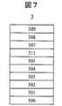
[実施例3]
図7は、本発明によるトンネル磁気抵抗効果素子の一例を示す断面模式図である。このトンネル磁気抵抗効果素子3は、下地膜300、配向制御膜301、反強磁性膜302、強磁性膜303、非磁性シード膜304、強磁性膜305、強磁性シード膜311、障壁膜307、強磁性膜308、保護膜309を積層して形成され、強磁性シード膜311に格子定数が障壁膜307の格子定数の1/√2よりも小さく、かつ強磁性膜305よりも大きい物質を配置することにより面積抵抗と磁気抵抗比が改善される。本実施例では、トンネル磁気抵抗効果素子はマグネトロンスパッタリング法を用いて作製し、成膜後300℃で磁界中でのアニール処理を施した。[Example 3]
FIG. 7 is a schematic cross-sectional view showing an example of a tunnel magnetoresistive effect element according to the present invention. The tunnel magnetoresistive
トンネル磁気抵抗効果素子3では、障壁膜307及び強磁性シード膜311を除いて、トンネル磁気抵抗効果素子2と同じ構造を持つ。障壁膜307にはMg0.5Ca0.5Oを、強磁性シード膜311にはCoFe(1.0nm)を用いている。強磁性シード膜311のCoの組成は、体心立方格子を持つ20atm%〜60atm%の間で使用した。Mg0.5Ca0.5Oの格子定数は0.449nmであり、その(001)面内格子間距離は1/√2倍の0.317nmとなるため、ここで用いた体心立方格子のCo0.25Fe0.75の格子定数である0.285nmよりも大きい。そのため、強磁性シード膜311を配置することにより、その上に積層する障壁膜307の格子定数も小さくなると考えられる。つまり、CoFeの格子定数がMg0.5Ca0.5Oよりも小さいため、非磁性シード膜304であるRhによる格子圧縮の効果と併せて、Mg0.5Ca0.5Oの格子間隔を縮小する歪みによってMg0.5Ca0.5Oの岩塩構造(001)配向の配向性をさらに向上させることが期待できる。The tunnel magnetoresistive
強磁性シード膜311は、Co,Fe,及びNiを少なくとも一種含む体心立方格子の強磁性体であってもよい。但し、CoFeなどにおいては膜厚が2nm以上になると体心立方構造の(110)配向が安定化するため、膜厚は2nm以下に設定することが望ましい。 The
Mg0.5Ca0.5Oを用いた磁気抵抗効果素子において、非磁性シード膜304に加えて障壁膜307の下に強磁性シード膜311であるCoFeを配置すると、面積抵抗RAは、ほぼ0.95kΩμm2とMgOの約1.15kΩμm2よりも大きく減少し、またTMR比は約130%とほぼMgOと同じTMR比を維持した。これは、CoFeを配置することによりMg0.5Ca0.5Oの結晶格子が小さくなる方向に歪み、結果として岩塩構造(001)配向が安定化し、MgOと同様にΔ1バンドの電子の選択的な透過が達成されているためと考えられる。In a magnetoresistive effect element using Mg0.5 Ca0.5 O, when CoFe which is a
[実施例4]
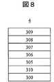
図8は、本発明によるトンネル磁気抵抗効果素子の一例を示す断面模式図である。このトンネル磁気抵抗効果素子4は、下地膜300、非磁性シード膜310、強磁性膜305、金属シード膜306、障壁膜307、強磁性膜308、保護膜309を積層して形成され、非磁性シード膜310を格子定数が強磁性膜305の格子定数の√2倍よりも小さく、かつ強磁性膜305よりも大きい面心立方格子の物質を用いることにより面積抵抗と磁気抵抗比が改善される。金属シード膜306として、特に障壁膜307で用いられた金属酸化物の金属を用いると、金属シード膜の一部酸化により障壁膜との接続性がよい。本実施例では、トンネル磁気抵抗効果素子はマグネトロンスパッタリング法を用いて作製し、成膜後300℃で磁界中でのアニール処理を施した。[Example 4]
FIG. 8 is a schematic sectional view showing an example of a tunnel magnetoresistive effect element according to the present invention. The tunnel magnetoresistive
本実施例における磁気抵抗効果素子4の構造は、実施例1の磁気抵抗効果素子1の障壁膜307の下に実施例2で用いたシード膜306を挿入した構造である。強磁性膜305は体心立方格子をもち、(001)配向したFe(5nm)を、強磁性膜308には体心立方格子をもち、(001)配向したFe(3nm)を用い、障壁膜307にはMgO(1.5nm)及びMgOとZnOの混晶であるMg0.7Zn0.3O(1.5nm)を用いた。非磁性シード膜310にはPd(3nm)を使用し、金属シード膜306にはMg(0.5nm)を用いた。Mgの格子定数は、0.321nmであり、障壁膜に圧縮歪みを与えるには十分小さいと考えられる。The structure of the
Mg0.7Zn0.3Oを用いた磁気抵抗効果素子において、障壁膜307の下に金属シード膜306であるMgを配置し、さらに強磁性膜305の下に非磁性シード膜であるPdを配置すると、面積抵抗RAは約0.48kΩμm2でTMR比〜135%となり、実施例1〜3のトンネル磁気抵抗効果素子1〜3よりも低抵抗かつ高TMR比を持つ素子を実現できた。これはMgとPdを配置することによりMg0.7Zn0.3Oの結晶格子が小さくなる方向に歪み、結果として岩塩構造(001)配向が安定化し、実施例1〜3のトンネル磁気抵抗効果素子1〜3よりもΔ1バンドの電子の選択的な透過が達成されているためと考えられる。金属シード膜306としては、Mg1-cZc(ZはZn,Cd,Ca,Sr,Ba,及びBの内から選んだ一種又は二種以上、0≦c≦1)からなり、格子定数が障壁膜307の格子定数よりも小さい膜を用いることができる。In the magnetoresistive effect element using Mg0.7 Zn0.3 O, when Mg as the
[実施例5]
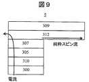
図9は、本発明による非局所スピン注入素子の一例を示す断面模式図である。この非局所スピン注入素子5は、下地膜300、非磁性シード膜310、強磁性膜305、障壁膜307、非磁性導電膜312、保護膜309を積層して形成されている。強磁性膜305は、(001)配向した体心立方格子の膜であり、障壁膜307は(001)配向した岩塩構造の酸化物の膜である。強磁性膜305はCo,Fe,及びNiを少なくとも一種含む材料で構成することができる。非磁性シード膜310に格子間隔が強磁性膜305の格子定数よりも小さい面心立方格子の物質を用いることにより、面積抵抗RAとスピン分極率が改善される。本実施例では、非局所スピン注入素子はマグネトロンスパッタリング法を用いて作製し、成膜後300℃で磁界中でのアニール処理を施した。[Example 5]
FIG. 9 is a schematic cross-sectional view showing an example of a non-local spin injection device according to the present invention. The non-local
下地膜300はTa(5nm)/Ru(10nm)/Ta(5nm)、保護膜309はTa(5nm)/Ru(5nm)により形成した。強磁性膜305にはFe(3nm)を用い、障壁膜307にはMgOとZnOの混晶であるMg0.7Zn0.3O(1.5nm)を用いた。非磁性シード膜310にはPd(3nm)を使用した。非磁性導電膜312にはCu(20nm)を使用した。The
非磁性シード膜310を用いない非局所スピン注入素子では、実施例1のトンネル磁気抵抗効果素子1と同様に、RA〜3.1kΩμm2とMgOを用いた素子の約3倍近くに上昇し、かつスピン分極率〜0.51と小さくなった。これはMg0.7Zn0.3Oの岩塩構造(001)配向が弱いため、障壁膜中での減衰率が小さいΔ1バンドの電子の選択的な透過を妨げてしまうことでRAが上昇し、またこの完全スピン分極しているΔ1バンドの電子の透過が妨げられたことでスピン分極率も減少していると考えられる。In the non-local spin injection device that does not use the
しかし、Mg0.7Zn0.3Oを用いた非局所スピン注入素子において、強磁性膜305であるFe膜の下にPd膜を配置すると、RA〜0.64kΩμm2とMgOよりも大きく減少し、またスピン分極率〜0.63とほぼMgOと同じスピン分極率を維持した。これはPd膜を配置することによりFeと共にMg0.7Zn0.3Oの結晶格子が小さくなる方向に歪み、結果として岩塩構造(001)配向が安定化し、MgOと同様にΔ1バンドの電子の選択的な透過が達成されているためと考えられる。However, in a non-local spin injection device using Mg0.7 Zn0.3 O, when a Pd film is disposed under the Fe film as the
障壁膜307は、Mg1-aXaO(XはZn,Cd,Ca,Sr,Ba,及びBの内から選んだ一種又は二種以上、0<a≦1)であってもよい。ここでXの組成割合が多ければ多い程バンドギャップは減少するが、その一方で混晶の岩塩構造はより不安定化する。そのため添加物Xに併せて、最適な組成aを選択する必要がある。The
非磁性シード膜310は、Pd,Rh,Pt,Al,Cu,Ag,Au,Ir,及びPbを少なくとも一種含んだ面心立方格子で、その格子定数が強磁性膜305の格子定数の√2倍よりも小さい材料、又はNa,V,Cr,Rb,Mo,Ba,及びWを少なくとも一種含んだ体心立方格子を持ち、その格子定数が強磁性膜305の格子定数よりも小さい金属であってもよい。但し、非磁性シード膜310の格子定数が強磁性膜305の格子定数に比べて極端に小さくなると、非磁性シード膜310と強磁性膜305の格子整合が保たれず、強磁性膜305の結晶格子歪みが起こらない。そのため、非磁性シード膜の格子定数は、強磁性膜305に格子整合させたときに、格子定数で数%程度小さい金属を選択する必要がある。 The
非磁性導電膜312は、スピン拡散長の長いAg,Cu,V,Pd,Auを少なくとも一種含んだ非磁性金属、又はGeやGaAs等の半導体であってもよい。 The nonmagnetic
非磁性シード膜310、強磁性膜305、障壁膜307には、トンネル磁気抵抗効果素子の実施例で説明した材料を用いることが可能である。また、トンネル磁気抵抗効果素子の実施例で説明したのと同様な構造を採用することもできる。例えば、強磁性膜305と障壁膜307との間に、(001)配向した岩塩構造のMg1-bYbO(YはZn,Cd,Ca,Sr,Ba,及びBの内から選んだ一種又は二種以上、0≦b<1)からなり、格子定数が障壁膜の格子定数よりも小さい絶縁シード膜を設けてもよい。また、強磁性膜305と障壁膜307との間に、Mg1-cZc(ZはZn,Cd,Ca,Sr,Ba,及びBの内から選んだ一種又は二種以上、0≦c≦1)からなり、格子定数が障壁膜の格子定数よりも小さい金属シード膜を設けてもよい。更に、強磁性膜305と障壁膜307との間に、Co,Fe,及びNiを少なくとも一種含む体心立方格子の強磁性体からなり、格子定数が障壁膜307の格子定数の1/√2倍よりも小さい強磁性シード膜を設けてもよい。For the
[実施例6]
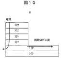
図10は、本発明による非局所スピン注入素子の一例を示す断面模式図である。この非局所スピン注入素子6は、下地膜300、非磁性シード膜310、障壁膜307、強磁性膜308、反強磁性膜302、保護膜309を積層して形成されている。強磁性膜308は、(001)配向した体心立方格子の膜であり、障壁膜307は(001)配向した岩塩構造の酸化物の膜である。強磁性膜305はCo,Fe,及びNiを少なくとも一種含む材料で構成することができる。非磁性シード膜310に格子間隔が障壁膜307の格子定数よりも小さい面心立方格子の物質を用いることにより、面積抵抗RAとスピン分極率が改善される。また、本実施例で用いられた非磁性シード膜307は、純粋スピン流の流れる非磁性導電膜にもなっている。本実施例では、非局所スピン注入素子はマグネトロンスパッタリング法を用いて作製し、成膜後300℃で磁界中でのアニール処理を施した。[Example 6]
FIG. 10 is a schematic cross-sectional view showing an example of a non-local spin injection device according to the present invention. The non-local
下地膜300はTa(5nm)/Ru(10nm)/Ta(5nm)、反強磁性膜302はMnIr(8nm)、保護膜309はTa(5nm)/Ru(5nm)により形成した。障壁膜307にはMgOとZnOの混晶であるMg0.7Zn0.3O(1.5nm)を用い、強磁性膜308にはFe(3nm)を用いた。非磁性シード膜310にはPd(20nm)を使用した。面心立方格子構造を持つPdの格子定数は0.389nmであり、岩塩構造を持つMg0.7Zn0.3Oの格子定数0.422nmよりも小さい。そのため、非磁性シード膜310としてPd膜を配置することにより、Pdを下地として育つ障壁膜307の格子定数も小さくなると考えられる。The
非磁性シード膜310に、障壁膜307を歪ませる効果が期待できないCu(20nm)を用いた非局所スピン注入素子では、実施例1のトンネル磁気抵抗効果素子1と同様に、RA〜3.1kΩμm2とMgOを用いた素子の約3倍近くに上昇し、かつスピン分極率〜0.51と小さくなった。これはMg0.7Zn0.3Oの岩塩構造(001)配向が弱いため、障壁膜中での減衰率が小さいΔ1バンドの電子の選択的な透過を妨げてしまうことでRAが上昇し、またこの完全スピン分極しているΔ1バンドの電子の透過が妨げられたことでスピン分極率も減少していると考えられる。In the non-local spin injection device using Cu (20 nm) that cannot be expected to distort the
しかし、障壁膜307にMg0.7Zn0.3Oを用いた非局所スピン注入素子において、障壁膜の下に非磁性シード膜としてPdを配置すると、RA〜0.48kΩμm2とMgOよりも大きく減少し、またスピン分極率〜0.63とほぼMgOと同じスピン分極率を維持した。これは、Pdを配置することによりMg0.7Zn0.3Oの結晶格子が小さくなる方向に歪み、結果として岩塩構造(001)配向が安定化し、MgOと同様にΔ1バンドの電子の選択的な透過が達成されているためと考えられる。However, in the non-local spin injection device using Mg0.7 Zn0.3 O for the
障壁膜307は、Mg1-aXaO(XはZn,Cd,Ca,Sr,Ba,及びBの内から選んだ一種又は二種以上、0<a≦1)であってもよい。ここでXの組成割合が多ければ多い程バンドギャップは減少するが、その一方で混晶の岩塩構造はより不安定化する。そのため添加物Xに併せて、最適な組成aを選択する必要がある。The
非磁性シード膜310は、Pd,Rh,Pt,Al,Cu,Ag,Au,Ir,及びPbを少なくとも一種含んだ障壁膜307よりも格子定数の小さい面心立方格子、又はNa,V,Cr,Rb,Mo,Ba,及びWを少なくとも一種含んだ、格子定数が障壁膜307の格子定数の1/√2倍よりも小さい体心立方格子を持つ金属であってもよい。 The
非磁性シード膜310、障壁膜307、強磁性膜308には、トンネル磁気抵抗効果素子の実施例で説明した材料を用いることも可能である。また、実施例2のトンネル磁気抵抗効果素子で用いた絶縁シード膜306を非磁性シード膜310と障壁膜307の間に設けることによって、障壁膜307の格子定数を縮めることも可能である。絶縁シード膜306は、Mg1-bYbO(YはZn,Cd,Ca,Sr,Ba,及びBの内から選んだ一種又は二種以上、0≦b<1)を用いることが可能である。ここで、Yの組成割合が多ければ多い程バンドギャップは減少するが、その一方で混晶の岩塩構造はより不安定化する。そのため添加物Yに併せて、最適な組成bを選択する必要がある。また、絶縁シード膜306であるMg1-bYbOの格子定数は、障壁膜307であるMg1-aXaOよりも小さくなくてはいけない。For the
[実施例7]
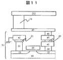
図11は、本発明による磁気メモリセルの構成例を示す断面模式図である。この磁気メモリセルは、メモリセルとして実施例1〜4に示したトンネル磁気抵抗効果素子1〜4のいずれか1種類の素子を搭載している。[Example 7]
FIG. 11 is a schematic cross-sectional view showing a configuration example of a magnetic memory cell according to the present invention. This magnetic memory cell is mounted with any one of the tunnel magnetoresistive
C−MOS11は、2つのn型半導体12,13と一つのp型半導体14からなる。n型半導体12にドレインとなる電極21が電気的に接続され、電極41,42を介してグラウンドに接続されている。n型半導体13には、ソースとなる電極22が電気的に接続されている。さらに23はゲート電極であり、このゲート電極23のON/OFFによりソース電極22とドレイン電極21の間の電流をON/OFF制御する。ソース電極22に電極43〜47が積層され、電極47を介してトンネル磁気抵抗効果素子10の下地膜300が接続されている。 The C-
ビット線212は、トンネル磁気抵抗効果素子10の保護膜309に接続されている。本実施例の磁気メモリセルでは、トンネル磁気抵抗効果素子10に流れる電流、いわゆるスピントランスファートルクによりトンネル磁気抵抗効果素子10の強磁性膜308の磁化方向を回転し、磁気的情報を記録する。また、スピントランスファートルクを用いずに、ビット線212とワード線を兼ねる電極42に電流を流し、その周りに作られる磁界を用いてトンネル磁気抵抗効果素子10の強磁性膜308の磁化方向を回転し、磁気的情報を記録してもよい。スピントランスファートルクにより書込みを行った場合、書込み時の電力は、電流磁界を用いた場合に比べ百分の一程度まで低減可能である。 The
図12は、上記磁気メモリセルを配置した不揮発性磁気メモリの構成例を示す図である。ゲート電極23とビット線212がメモリセル100に電気的に接続されている。上記の磁気メモリセルを配置することにより、磁気メモリは低消費電力で動作が可能であり、ギガビット級の高密度磁気メモリを実現可能である。 FIG. 12 is a diagram showing a configuration example of a nonvolatile magnetic memory in which the magnetic memory cells are arranged. The
[実施例8]
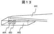
図13は、本発明による記録・再生磁気ヘッドの構成例を示す模式図である。この記録・再生磁気ヘッドは、再生磁気ヘッドとして、実施例1〜4に示したトンネル磁気抵抗効果素子1〜4、あるいは実施例5,6に示した非局所スピン注入素子5,6のいずれか1つを搭載している。601はスライダアーム、602は磁気ヘッド、603は本実施例に係る再生ヘッド部位、604は垂直記録方式やエネルギーアシストによる記録ヘッド部位をそれぞれ示す。[Example 8]
FIG. 13 is a schematic diagram showing a configuration example of a recording / reproducing magnetic head according to the present invention. As the reproducing magnetic head, this recording / reproducing magnetic head is one of the tunnel magnetoresistive
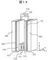
次に、本発明のトンネル磁気抵抗効果素子を用いた再生ヘッドの構成例について説明する。図14は、トンネル磁気抵抗効果素子を用いた再生ヘッドの一例を示す模式図である。一対の電極層510,517の媒体対向面側の一端に、強磁性層の磁化を固定するための反強磁性層515、強磁性固定層514、障壁層511、強磁性自由層512からなるトンネル磁気抵抗効果素子を搭載している。電極層510,517は、絶縁層530及び531を介して、磁気シールド540,541に接触している。電流源519により、トンネル磁気抵抗効果素子にトンネル電流が流れ、電圧計518により電圧を計測する。このとき、記録媒体からの漏洩磁界により強磁性自由層512の磁化の向きが変化し、その磁化の向きによってトンネル磁気抵抗効果素子の抵抗値が大きく変化する。この抵抗変化による検出電圧の変化を通して、記録媒体の磁化方向を検出する。図14に機能的に図示したトンネル磁気抵抗効果素子として、実施例1〜4に示したトンネル磁気抵抗効果素子1〜4を用いることができる。 Next, a configuration example of a read head using the tunnel magnetoresistive element of the present invention will be described. FIG. 14 is a schematic diagram showing an example of a read head using a tunnel magnetoresistive element. A tunnel composed of an
次に、本発明によるスピン蓄積素子用いた再生ヘッドの構成例について説明する。図15は、スピン蓄積素子用いた再生ヘッドの一例を示す模式図である。非磁性導電層である電極層510の媒体対向面側の一端上に、障壁層511を介して積層された強磁性自由層512と、電極層510の他端上に、障壁層513を介して積層された強磁性固定層514と、強磁性固定層514の磁化を固定するための反強磁性層515、反強磁性層515に接続されている電極層517からなるスピン蓄積素子を搭載している。電極層510,517は絶縁層530,531を介して、磁気シールド540,541に接触している。強磁性自由層512は絶縁層を介さずに磁気シールド541に接触しており、磁気シールド541が電極として動作する。電流源519により、障壁層513を通って強磁性固定層514と電極層510との間にトンネル電流が流れ、電極層510に純粋スピン流が注入される。また、記録媒体からの漏洩磁界により強磁性自由層512の磁化の向きが変化する。強磁性自由層512と強磁性固定層514との間の相対的な磁化の向きに依存して発生する電圧を、電極層510と強磁性自由層512に接続されている磁気シールド541との間に生じる電圧として電圧計518により検出する。図15に機能的に図示した非局所スピン注入素子(510,513,514,515)として、実施例5,6に示した非局所スピン注入素子5,6を用いることができる。 Next, a configuration example of a read head using the spin accumulation element according to the present invention will be described. FIG. 15 is a schematic diagram showing an example of a reproducing head using a spin accumulation element. A ferromagnetic
図16は、上記磁気ヘッドを備える磁気記録再生装置の構成例を示した模式図である。この磁気記録再生装置は、長手記録連続媒体、垂直記録連続媒体、ディスクリート媒体、パターン媒体といった磁気記録層を有する磁気記録媒体701と、記録媒体を駆動する駆動部702と、図13で示した磁気ヘッド602と、磁気ヘッド602を磁気記録媒体701上の所定の位置へ移動させるアクチュエータ703及びスライダアーム601と、磁気ヘッドからの出力信号を処理する信号処理部710と、駆動部702及びアクチュエータ703を制御する制御部720を備える。 FIG. 16 is a schematic diagram showing a configuration example of a magnetic recording / reproducing apparatus including the magnetic head. This magnetic recording / reproducing apparatus includes a
磁気記録再生装置は、スピンドルモータ等の駆動部702によって、磁気記録媒体701を回転させ、磁気ヘッド602による記録再生を行う。磁気ヘッド602から出力される信号に適切な信号処理を施すことにより、磁気記録媒体701に記録された磁気情報を読み取ることが可能となる。 In the magnetic recording / reproducing apparatus, a
なお、本発明は上記した実施例に限定されるものではなく、様々な変形例が含まれる。例えば、上記した実施例は本発明を分かりやすく説明するために詳細に説明したものであり、必ずしも説明した全ての構成を備えるものに限定されるものではない。また、ある実施例の構成の一部を他の実施例の構成に置き換えることが可能であり、また、ある実施例の構成に他の実施例の構成を加えることも可能である。また、各実施例の構成の一部について、他の構成の追加・削除・置換をすることが可能である。 In addition, this invention is not limited to an above-described Example, Various modifications are included. For example, the above-described embodiments have been described in detail for easy understanding of the present invention, and are not necessarily limited to those having all the configurations described. Further, a part of the configuration of one embodiment can be replaced with the configuration of another embodiment, and the configuration of another embodiment can be added to the configuration of one embodiment. Further, it is possible to add, delete, and replace other configurations for a part of the configuration of each embodiment.
1〜4…トンネル磁気抵抗効果素子、10…トンネル磁気抵抗効果素子、11…トランジスタ、12,13…n型半導体、14…p型半導体、21…ドレイン電極、22…ソース電極、23…ゲート電極、41〜47…電極、60…電極、61…漏れ磁界、63…対向面、71…コイル、72…記録トラック、81…上部コア、91…記録媒体、100…基板、211…書込みワード線、212…ビット線、300…下地膜、301…配向性制御膜、302…反強磁性膜、303…強磁性膜、304…非磁性膜、305…強磁性膜、306…シード膜、307…障壁膜、308…強磁性膜、309…保護膜、310…非磁性シード膜、311…強磁性シード膜、510…電極、511…障壁層、512…強磁性自由層、513…障壁層、514…磁化固定層、515…反強磁性層、517…電極、518…電圧計、519…電流源、530,531…絶縁層、540,541…シールド層、601…スライダアーム、602…磁気ヘッド、603…再生部位、604…記録部位、701…磁気記録媒体、702…駆動部、703…アクチュエータ、710…信号処理部、720…制御部DESCRIPTION OF SYMBOLS 1-4 ... Tunnel magnetoresistive effect element, 10 ... Tunnel magnetoresistive effect element, 11 ... Transistor, 12, 13 ... N-type semiconductor, 14 ... P-type semiconductor, 21 ... Drain electrode, 22 ... Source electrode, 23 ...
Claims (13)
Translated fromJapanese前記第一の強磁性膜の上に設けられた障壁膜と、
前記障壁膜の上に設けられた第二の強磁性膜と、
前記第一の強磁性膜の下に設けられた非磁性シード膜とを有し、
前記第一の強磁性膜と前記第二の強磁性膜は(001)配向した体心立方格子の膜、前記障壁膜は(001)配向した岩塩構造のMg1-aXaO(XはZn,Cd,Ca,Sr,Ba,及びBの内から選んだ一種又は二種以上、0<a≦1)の膜であり、前記非磁性シード膜は前記第一の強磁性膜と格子整合し、かつ前記第一の強磁性膜と格子整合した格子間距離が前記第一の強磁性膜より小さい非磁性金属膜であることを特徴とするトンネル磁気抵抗効果素子。A first ferromagnetic film;
A barrier film provided on the first ferromagnetic film;
A second ferromagnetic film provided on the barrier film;
A non-magnetic seed film provided under the first ferromagnetic film,
The first ferromagnetic film and the second ferromagnetic film are (001) oriented body-centered cubic lattice films, and the barrier film is a (001) oriented rock salt structureMg1-aXaO (X is One or more selected from Zn, Cd, Ca, Sr, Ba, and B, 0 <a ≦ 1) , and the nonmagnetic seed film islattice-matched with the first ferromagnetic film And a nonmagnetic metal film having alattice-matching distance lattice-matched to the first ferromagnetic film that is smaller than the first ferromagnetic film .
前記トンネル磁気抵抗効果素子は、第一の強磁性膜と、前記第一の強磁性膜の上に設けられた障壁膜と、前記障壁膜の上に設けられた第二の強磁性膜と、前記第一の強磁性膜の下に設けられた非磁性シード膜とを有し、前記第一の強磁性膜と前記第二の強磁性膜は(001)配向した体心立方格子の膜、前記障壁膜は(001)配向した岩塩構造のMg1-aXaO(XはZn,Cd,Ca,Sr,Ba,及びBの内から選んだ一種又は二種以上、0<a≦1)の膜であり、前記非磁性シード膜は前記第一の強磁性膜と格子整合し、かつ前記第一の強磁性膜と格子整合した格子間距離が前記第一の強磁性膜より小さい非磁性金属膜であることを特徴とする磁気ヘッド。In a magnetic head having a recording unit having a magnetic pole for generating a recording magnetic field and a reproducing unit including a tunnel magnetoresistive element,
The tunnel magnetoresistive element includes a first ferromagnetic film, a barrier film provided on the first ferromagnetic film, a second ferromagnetic film provided on the barrier film, A nonmagnetic seed film provided under the first ferromagnetic film, wherein the first ferromagnetic film and the second ferromagnetic film are (001) oriented body-centered cubic lattice films, the barrier film(001) Mg 1-a X a O (X -oriented rock saltstructure Zn, Cd, Ca, Sr, Ba,and one or two or more selected from among B, 0 <a ≦ 1 The nonmagnetic seed film islattice-matched with the first ferromagnetic film, and the interstitial distance lattice-matched with the first ferromagnetic film is smaller than the first ferromagnetic film. A magnetic head comprising a magnetic metal film.
前記強磁性膜は(001)配向した体心立方格子の膜、前記障壁膜は(001)配向した岩塩構造のMg1-aXaO(XはZn,Cd,Ca,Sr,Ba,及びBの内から選んだ一種又は二種以上、0<a≦1)の膜であり、前記非磁性シード膜は前記強磁性膜と格子整合し、かつ前記強磁性膜と格子整合した格子間距離が前記強磁性膜より小さい非磁性金属膜であることを特徴とする非局所スピン注入素子。A ferromagnetic film, a barrier film provided on the ferromagnetic film, a nonmagnetic conductive film provided on the barrier film, and a nonmagnetic seed film provided below the ferromagnetic film. In a non-local spin injection device having
The ferromagnetic film (001) -oriented body-centered cubic lattice of the film, the barrier film(001) Mg 1-a X a O (X -oriented rock saltstructure Zn, Cd, Ca, Sr, Ba, and 1 or 2 or more selected from B, 0 <a ≦ 1) , and the nonmagnetic seed film islattice-matched with the ferromagnetic film and lattice-matched with the ferromagnetic film Is a nonmagnetic metal filmsmaller than the ferromagnetic film .
前記非局所スピン注入素子は、強磁性膜と、前記強磁性膜の上に設けられた障壁膜と、前記障壁膜の上に設けられた非磁性導電膜と、前記強磁性膜の下に設けられた非磁性シード膜とを有し、前記強磁性膜は(001)配向した体心立方格子の膜、前記障壁膜は(001)配向した岩塩構造のMg1-aXaO(XはZn,Cd,Ca,Sr,Ba,及びBの内から選んだ一種又は二種以上、0<a≦1)の膜であり、前記非磁性シード膜は前記強磁性膜と格子整合し、かつ前記強磁性膜と格子整合した格子間距離が前記強磁性膜より小さい非磁性金属膜であることを特徴とする磁気ヘッド。In a magnetic head having a recording unit having a magnetic pole for generating a recording magnetic field and a reproducing unit having a non-local spin injection element,
The non-local spin injection device is provided under a ferromagnetic film, a barrier film provided on the ferromagnetic film, a nonmagnetic conductive film provided on the barrier film, and the ferromagnetic film. The ferromagnetic film is a (001) oriented body-centered cubic lattice film, and the barrier film is a (001) oriented rock salt structureMg1-aXaO (X is One or more selected from Zn, Cd, Ca, Sr, Ba, and B, 0 <a ≦ 1) , wherein the nonmagnetic seed film islattice-matched with the ferromagnetic film, and A magnetic head,wherein the interstitial distance lattice-matched with the ferromagnetic film is a nonmagnetic metal filmsmaller than the ferromagnetic film .
Priority Applications (1)
| Application Number | Priority Date | Filing Date | Title |
|---|---|---|---|
| JP2011180588AJP5705683B2 (en) | 2011-08-22 | 2011-08-22 | Tunnel magnetoresistive element, non-local spin injection element, and magnetic head using the same |
Applications Claiming Priority (1)
| Application Number | Priority Date | Filing Date | Title |
|---|---|---|---|
| JP2011180588AJP5705683B2 (en) | 2011-08-22 | 2011-08-22 | Tunnel magnetoresistive element, non-local spin injection element, and magnetic head using the same |
Publications (2)
| Publication Number | Publication Date |
|---|---|
| JP2013045800A JP2013045800A (en) | 2013-03-04 |
| JP5705683B2true JP5705683B2 (en) | 2015-04-22 |
Family
ID=48009500
Family Applications (1)
| Application Number | Title | Priority Date | Filing Date |
|---|---|---|---|
| JP2011180588AExpired - Fee RelatedJP5705683B2 (en) | 2011-08-22 | 2011-08-22 | Tunnel magnetoresistive element, non-local spin injection element, and magnetic head using the same |
Country Status (1)
| Country | Link |
|---|---|
| JP (1) | JP5705683B2 (en) |
Families Citing this family (2)
| Publication number | Priority date | Publication date | Assignee | Title |
|---|---|---|---|---|
| JP6640766B2 (en)* | 2017-02-07 | 2020-02-05 | 株式会社東芝 | Magnetic element, pressure sensor, magnetic head, and magnetic memory |
| JP6299897B2 (en)* | 2017-02-13 | 2018-03-28 | Tdk株式会社 | Tunnel layer |
Family Cites Families (10)
| Publication number | Priority date | Publication date | Assignee | Title |
|---|---|---|---|---|
| JP4834834B2 (en)* | 2006-05-08 | 2011-12-14 | 国立大学法人東北大学 | Tunnel magnetoresistive element, nonvolatile magnetic memory, light emitting element, and three-terminal element |
| JP4496189B2 (en)* | 2006-09-28 | 2010-07-07 | 株式会社東芝 | Magnetoresistive element and magnetoresistive random access memory |
| US8031441B2 (en)* | 2007-05-11 | 2011-10-04 | Headway Technologies, Inc. | CPP device with an enhanced dR/R ratio |
| JP5181388B2 (en)* | 2008-03-31 | 2013-04-10 | 秋田県 | Ferromagnetic laminated structure and manufacturing method thereof |
| JP2009302378A (en)* | 2008-06-16 | 2009-12-24 | Fujitsu Ltd | Tunnel magnetic resistive effect element and magnetic resistive device using the same |
| WO2010026667A1 (en)* | 2008-09-03 | 2010-03-11 | Canon Anelva Corporation | Ferromagnetic preferred grain growth promotion seed layer for amorphous or microcrystalline mgo tunnel barrier |
| JP2012502447A (en)* | 2008-09-03 | 2012-01-26 | キヤノンアネルバ株式会社 | Preferred grain grown ferromagnetic seed layer for amorphous or microcrystalline MgO tunnel barriers |
| JP2010109208A (en)* | 2008-10-31 | 2010-05-13 | Fujitsu Ltd | Tunnel magnetoresistive effect element and magnetoresistive device |
| EP2405504B1 (en)* | 2009-03-04 | 2014-12-17 | Hitachi, Ltd. | Magnetic memory |
| JP2011123923A (en)* | 2009-12-08 | 2011-06-23 | Hitachi Global Storage Technologies Netherlands Bv | Magnetoresistive effect head, magnetic recording/reproducing device |
- 2011
- 2011-08-22JPJP2011180588Apatent/JP5705683B2/ennot_activeExpired - Fee Related
Also Published As
| Publication number | Publication date |
|---|---|
| JP2013045800A (en) | 2013-03-04 |
Similar Documents
| Publication | Publication Date | Title |
|---|---|---|
| JP5096702B2 (en) | Magnetoresistive element and nonvolatile magnetic memory equipped with the same | |
| JP5337817B2 (en) | Magnetoresistive element, magnetic memory cell and magnetic random access memory using the same | |
| JP5123365B2 (en) | Magnetoresistive element and magnetic memory | |
| JP4745414B2 (en) | Magnetoresistive element and magnetic memory | |
| US7777261B2 (en) | Magnetic device having stabilized free ferromagnetic layer | |
| US9042165B2 (en) | Magnetoresistive effect element, magnetic memory cell using same, and random access memory | |
| US9006704B2 (en) | Magnetic element with improved out-of-plane anisotropy for spintronic applications | |
| JP5143444B2 (en) | Magnetoresistive element, magnetic memory cell and magnetic random access memory using the same | |
| US20120320666A1 (en) | Magnetoresistive Element and Magnetic Memory | |
| JP2009027177A (en) | STT-MTJ-MRAM cell and manufacturing method thereof | |
| KR20090059038A (en) | Thermal-Assisted Write Magnetic Element | |
| JP2007294737A (en) | Tunnel magnetoresistive element, magnetic memory cell and random access memory using the same | |
| US8644058B2 (en) | Spin-injection element, and magnetic field sensor and magnetic recording memory employing the same | |
| US9053800B2 (en) | Memory element and memory apparatus | |
| WO2009110119A1 (en) | Ferromagnetic tunnel junction element and driving method of ferromagnetic tunnel junction element | |
| US20240032437A1 (en) | Buffer Layers, Interlayers, and Barrier Layers Comprising Heusler Alloys for SOT Based Sensor, Memory, and Storage Devices | |
| JP6803575B2 (en) | Magnetoresistance element using I-III-VI2 compound semiconductor and manufacturing method thereof, magnetic storage device and spin transistor using the same - Patents.com | |
| JP2008091551A (en) | Magnetoresistive element, magnetic storage device, and magnetic memory device | |
| JP5705683B2 (en) | Tunnel magnetoresistive element, non-local spin injection element, and magnetic head using the same | |
| WO2012014415A1 (en) | Low-resistance and high-efficiency spin injection element using thin film of rock salt structure as seed | |
| JP5562946B2 (en) | Tunnel magnetoresistive element, magnetic memory cell and random access memory using the same | |
| US20220246836A1 (en) | Composite recording structure for an improved write profermance | |
| JP7127770B2 (en) | A perpendicular magnetization ferromagnetic semiconductor heterojunction device, a magnetic memory device using the same, and a spin logic device | |
| JP2013016820A (en) | Tunnel magnetoresistance effect element, and magnetic memory cell and random access memory including the same | |
| JP5030888B2 (en) | Resonant tunnel magnetoresistive element, magnetic memory cell, and magnetic random access memory |
Legal Events
| Date | Code | Title | Description |
|---|---|---|---|
| A621 | Written request for application examination | Free format text:JAPANESE INTERMEDIATE CODE: A621 Effective date:20131107 | |
| A131 | Notification of reasons for refusal | Free format text:JAPANESE INTERMEDIATE CODE: A131 Effective date:20141021 | |
| A521 | Request for written amendment filed | Free format text:JAPANESE INTERMEDIATE CODE: A523 Effective date:20141205 | |
| TRDD | Decision of grant or rejection written | ||
| A01 | Written decision to grant a patent or to grant a registration (utility model) | Free format text:JAPANESE INTERMEDIATE CODE: A01 Effective date:20150127 | |
| A61 | First payment of annual fees (during grant procedure) | Free format text:JAPANESE INTERMEDIATE CODE: A61 Effective date:20150225 | |
| R151 | Written notification of patent or utility model registration | Ref document number:5705683 Country of ref document:JP Free format text:JAPANESE INTERMEDIATE CODE: R151 | |
| LAPS | Cancellation because of no payment of annual fees |