JP5703431B2 - Method for forming inorganic / organic hybrid nanolaminate barrier film - Google Patents
Method for forming inorganic / organic hybrid nanolaminate barrier filmDownload PDFInfo
- Publication number
- JP5703431B2 JP5703431B2JP2006538120AJP2006538120AJP5703431B2JP 5703431 B2JP5703431 B2JP 5703431B2JP 2006538120 AJP2006538120 AJP 2006538120AJP 2006538120 AJP2006538120 AJP 2006538120AJP 5703431 B2JP5703431 B2JP 5703431B2
- Authority
- JP
- Japan
- Prior art keywords
- mixture
- coating
- fluorinated
- polymer
- polymer precursor
- Prior art date
- Legal status (The legal status is an assumption and is not a legal conclusion. Google has not performed a legal analysis and makes no representation as to the accuracy of the status listed.)
- Expired - Fee Related
Links
- 230000004888barrier functionEffects0.000titleclaimsdescription40
- 238000000034methodMethods0.000titleclaimsdescription22
- LFQSCWFLJHTTHZ-UHFFFAOYSA-NEthanolChemical compoundCCOLFQSCWFLJHTTHZ-UHFFFAOYSA-N0.000claimsdescription27
- 239000002243precursorSubstances0.000claimsdescription25
- 238000000576coating methodMethods0.000claimsdescription23
- 229920000642polymerPolymers0.000claimsdescription23
- XLYOFNOQVPJJNP-UHFFFAOYSA-NwaterSubstancesOXLYOFNOQVPJJNP-UHFFFAOYSA-N0.000claimsdescription20
- 239000000203mixtureSubstances0.000claimsdescription16
- 239000004094surface-active agentSubstances0.000claimsdescription16
- 239000011248coating agentSubstances0.000claimsdescription15
- 239000000758substrateSubstances0.000claimsdescription11
- 239000000463materialSubstances0.000claimsdescription10
- BOTDANWDWHJENH-UHFFFAOYSA-NTetraethyl orthosilicateChemical compoundCCO[Si](OCC)(OCC)OCCBOTDANWDWHJENH-UHFFFAOYSA-N0.000claimsdescription8
- 125000001165hydrophobic groupChemical group0.000claimsdescription8
- 150000004703alkoxidesChemical class0.000claimsdescription7
- 238000001704evaporationMethods0.000claimsdescription7
- 239000000693micelleSubstances0.000claimsdescription7
- -1polyethylene naphthalatePolymers0.000claimsdescription7
- VEXZGXHMUGYJMC-UHFFFAOYSA-NHydrochloric acidChemical compoundClVEXZGXHMUGYJMC-UHFFFAOYSA-N0.000claimsdescription6
- DKAGJZJALZXOOV-UHFFFAOYSA-Nhydrate;hydrochlorideChemical compoundO.ClDKAGJZJALZXOOV-UHFFFAOYSA-N0.000claimsdescription5
- 239000011368organic materialSubstances0.000claimsdescription5
- LZZYPRNAOMGNLH-UHFFFAOYSA-MCetrimonium bromideChemical group[Br-].CCCCCCCCCCCCCCCC[N+](C)(C)CLZZYPRNAOMGNLH-UHFFFAOYSA-M0.000claimsdescription4
- 239000004696Poly ether ether ketoneSubstances0.000claimsdescription4
- 150000001450anionsChemical class0.000claimsdescription4
- IISBACLAFKSPIT-UHFFFAOYSA-Nbisphenol AChemical compoundC=1C=C(O)C=CC=1C(C)(C)C1=CC=C(O)C=C1IISBACLAFKSPIT-UHFFFAOYSA-N0.000claimsdescription4
- 150000001768cationsChemical class0.000claimsdescription4
- 239000007822coupling agentSubstances0.000claimsdescription4
- 238000000151depositionMethods0.000claimsdescription4
- 239000003999initiatorSubstances0.000claimsdescription4
- 229920002530polyetherether ketonePolymers0.000claimsdescription4
- 239000011112polyethylene naphthalateSubstances0.000claimsdescription4
- XDLMVUHYZWKMMD-UHFFFAOYSA-N3-trimethoxysilylpropyl 2-methylprop-2-enoateChemical compoundCO[Si](OC)(OC)CCCOC(=O)C(C)=CXDLMVUHYZWKMMD-UHFFFAOYSA-N0.000claimsdescription3
- 230000015572biosynthetic processEffects0.000claimsdescription3
- 238000003618dip coatingMethods0.000claimsdescription3
- 229920000058polyacrylatePolymers0.000claimsdescription3
- 238000004528spin coatingMethods0.000claimsdescription3
- RKLXSINPXIQKIB-UHFFFAOYSA-Ntrimethoxy(oct-7-enyl)silaneChemical groupCO[Si](OC)(OC)CCCCCCC=CRKLXSINPXIQKIB-UHFFFAOYSA-N0.000claimsdescription3
- 229910020366ClO 4Inorganic materials0.000claimsdescription2
- QNAYBMKLOCPYGJ-REOHCLBHSA-NL-alanineChemical compoundC[C@H](N)C(O)=OQNAYBMKLOCPYGJ-REOHCLBHSA-N0.000claimsdescription2
- AGPKZVBTJJNPAG-WHFBIAKZSA-NL-isoleucineChemical compoundCC[C@H](C)[C@H](N)C(O)=OAGPKZVBTJJNPAG-WHFBIAKZSA-N0.000claimsdescription2
- ROHFNLRQFUQHCH-YFKPBYRVSA-NL-leucineChemical compoundCC(C)C[C@H](N)C(O)=OROHFNLRQFUQHCH-YFKPBYRVSA-N0.000claimsdescription2
- FFEARJCKVFRZRR-BYPYZUCNSA-NL-methionineChemical compoundCSCC[C@H](N)C(O)=OFFEARJCKVFRZRR-BYPYZUCNSA-N0.000claimsdescription2
- COLNVLDHVKWLRT-QMMMGPOBSA-NL-phenylalanineChemical compoundOC(=O)[C@@H](N)CC1=CC=CC=C1COLNVLDHVKWLRT-QMMMGPOBSA-N0.000claimsdescription2
- QIVBCDIJIAJPQS-VIFPVBQESA-NL-tryptophaneChemical compoundC1=CC=C2C(C[C@H](N)C(O)=O)=CNC2=C1QIVBCDIJIAJPQS-VIFPVBQESA-N0.000claimsdescription2
- OUYCCCASQSFEME-QMMMGPOBSA-NL-tyrosineChemical compoundOC(=O)[C@@H](N)CC1=CC=C(O)C=C1OUYCCCASQSFEME-QMMMGPOBSA-N0.000claimsdescription2
- KZSNJWFQEVHDMF-BYPYZUCNSA-NL-valineChemical compoundCC(C)[C@H](N)C(O)=OKZSNJWFQEVHDMF-BYPYZUCNSA-N0.000claimsdescription2
- ROHFNLRQFUQHCH-UHFFFAOYSA-NLeucineNatural productsCC(C)CC(N)C(O)=OROHFNLRQFUQHCH-UHFFFAOYSA-N0.000claimsdescription2
- 239000004695Polyether sulfoneSubstances0.000claimsdescription2
- QIVBCDIJIAJPQS-UHFFFAOYSA-NTryptophanNatural productsC1=CC=C2C(CC(N)C(O)=O)=CNC2=C1QIVBCDIJIAJPQS-UHFFFAOYSA-N0.000claimsdescription2
- KZSNJWFQEVHDMF-UHFFFAOYSA-NValineNatural productsCC(C)C(N)C(O)=OKZSNJWFQEVHDMF-UHFFFAOYSA-N0.000claimsdescription2
- 235000004279alanineNutrition0.000claimsdescription2
- 238000000137annealingMethods0.000claimsdescription2
- 125000001797benzyl groupChemical group[H]C1=C([H])C([H])=C(C([H])=C1[H])C([H])([H])*0.000claimsdescription2
- 238000006243chemical reactionMethods0.000claimsdescription2
- 238000000354decomposition reactionMethods0.000claimsdescription2
- 238000010438heat treatmentMethods0.000claimsdescription2
- 229960000310isoleucineDrugs0.000claimsdescription2
- AGPKZVBTJJNPAG-UHFFFAOYSA-NisoleucineNatural productsCCC(C)C(N)C(O)=OAGPKZVBTJJNPAG-UHFFFAOYSA-N0.000claimsdescription2
- 229930182817methionineNatural products0.000claimsdescription2
- 125000002496methyl groupChemical group[H]C([H])([H])*0.000claimsdescription2
- 238000002156mixingMethods0.000claimsdescription2
- COLNVLDHVKWLRT-UHFFFAOYSA-NphenylalanineNatural productsOC(=O)C(N)CC1=CC=CC=C1COLNVLDHVKWLRT-UHFFFAOYSA-N0.000claimsdescription2
- 229920003207poly(ethylene-2,6-naphthalate)Polymers0.000claimsdescription2
- 229920006393polyether sulfonePolymers0.000claimsdescription2
- 230000008569processEffects0.000claimsdescription2
- 230000002940repellentEffects0.000claimsdescription2
- 239000005871repellentSubstances0.000claimsdescription2
- 238000005507sprayingMethods0.000claimsdescription2
- OUYCCCASQSFEME-UHFFFAOYSA-NtyrosineNatural productsOC(=O)C(N)CC1=CC=C(O)C=C1OUYCCCASQSFEME-UHFFFAOYSA-N0.000claimsdescription2
- 239000004474valineSubstances0.000claimsdescription2
- 229920000620organic polymerPolymers0.000claims3
- 239000003431cross linking reagentSubstances0.000claims1
- 230000003247decreasing effectEffects0.000claims1
- QROGIFZRVHSFLM-UHFFFAOYSA-Nprop-1-enylbenzeneChemical classCC=CC1=CC=CC=C1QROGIFZRVHSFLM-UHFFFAOYSA-N0.000claims1
- 150000003440styrenesChemical class0.000claims1
- 239000010408filmSubstances0.000description32
- 239000010410layerSubstances0.000description32
- QVGXLLKOCUKJST-UHFFFAOYSA-Natomic oxygenChemical compound[O]QVGXLLKOCUKJST-UHFFFAOYSA-N0.000description10
- 229910052760oxygenInorganic materials0.000description10
- 239000001301oxygenSubstances0.000description10
- 230000035699permeabilityEffects0.000description9
- 239000012044organic layerSubstances0.000description8
- 239000000178monomerSubstances0.000description6
- 230000008020evaporationEffects0.000description5
- 230000005693optoelectronicsEffects0.000description5
- 238000001338self-assemblyMethods0.000description5
- PPBRXRYQALVLMV-UHFFFAOYSA-NStyreneChemical compoundC=CC1=CC=CC=C1PPBRXRYQALVLMV-UHFFFAOYSA-N0.000description4
- 230000002209hydrophobic effectEffects0.000description4
- 239000004033plasticSubstances0.000description4
- 229920003023plasticPolymers0.000description4
- 239000003795chemical substances by applicationSubstances0.000description3
- 229910010272inorganic materialInorganic materials0.000description3
- 239000011147inorganic materialSubstances0.000description3
- 230000003993interactionEffects0.000description3
- 239000010409thin filmSubstances0.000description3
- 239000010936titaniumSubstances0.000description3
- OGBWMWKMTUSNKE-UHFFFAOYSA-N1-(2-methylprop-2-enoyloxy)hexyl 2-methylprop-2-enoateChemical compoundCCCCCC(OC(=O)C(C)=C)OC(=O)C(C)=COGBWMWKMTUSNKE-UHFFFAOYSA-N0.000description2
- YGYNBBAUIYTWBF-UHFFFAOYSA-N2,6-dimethylnaphthaleneChemical compoundC1=C(C)C=CC2=CC(C)=CC=C21YGYNBBAUIYTWBF-UHFFFAOYSA-N0.000description2
- JLBJTVDPSNHSKJ-UHFFFAOYSA-N4-MethylstyreneChemical compoundCC1=CC=C(C=C)C=C1JLBJTVDPSNHSKJ-UHFFFAOYSA-N0.000description2
- 239000004971Cross linkerSubstances0.000description2
- LCGLNKUTAGEVQW-UHFFFAOYSA-NDimethyl etherChemical compoundCOCLCGLNKUTAGEVQW-UHFFFAOYSA-N0.000description2
- 229920012266Poly(ether sulfone) PESPolymers0.000description2
- KYIKRXIYLAGAKQ-UHFFFAOYSA-NabcnChemical compoundC1CCCCC1(C#N)N=NC1(C#N)CCCCC1KYIKRXIYLAGAKQ-UHFFFAOYSA-N0.000description2
- ISAOCJYIOMOJEB-UHFFFAOYSA-NbenzoinChemical compoundC=1C=CC=CC=1C(O)C(=O)C1=CC=CC=C1ISAOCJYIOMOJEB-UHFFFAOYSA-N0.000description2
- 230000005540biological transmissionEffects0.000description2
- 230000007613environmental effectEffects0.000description2
- 239000007789gasSubstances0.000description2
- 239000011521glassSubstances0.000description2
- 229910052751metalInorganic materials0.000description2
- 239000002184metalSubstances0.000description2
- 239000002114nanocompositeSubstances0.000description2
- 229920000139polyethylene terephthalatePolymers0.000description2
- 239000005020polyethylene terephthalateSubstances0.000description2
- 238000002360preparation methodMethods0.000description2
- 238000003980solgel methodMethods0.000description2
- 229910052719titaniumInorganic materials0.000description2
- VXUYXOFXAQZZMF-UHFFFAOYSA-Ntitanium(IV) isopropoxideChemical compoundCC(C)O[Ti](OC(C)C)(OC(C)C)OC(C)CVXUYXOFXAQZZMF-UHFFFAOYSA-N0.000description2
- NIXOWILDQLNWCW-UHFFFAOYSA-MAcrylateChemical compound[O-]C(=O)C=CNIXOWILDQLNWCW-UHFFFAOYSA-M0.000description1
- 229910018072Al 2 O 3Inorganic materials0.000description1
- 102100020870La-related protein 6Human genes0.000description1
- 108050008265La-related protein 6Proteins0.000description1
- 239000004976Lyotropic liquid crystalSubstances0.000description1
- BPQQTUXANYXVAA-UHFFFAOYSA-NOrthosilicateChemical compound[O-][Si]([O-])([O-])[O-]BPQQTUXANYXVAA-UHFFFAOYSA-N0.000description1
- 229910052581Si3N4Inorganic materials0.000description1
- 229910004298SiO 2Inorganic materials0.000description1
- XUIMIQQOPSSXEZ-UHFFFAOYSA-NSiliconChemical compound[Si]XUIMIQQOPSSXEZ-UHFFFAOYSA-N0.000description1
- 244000028419Styrax benzoinSpecies0.000description1
- 235000000126Styrax benzoinNutrition0.000description1
- 235000008411Sumatra benzointreeNutrition0.000description1
- RTAQQCXQSZGOHL-UHFFFAOYSA-NTitaniumChemical compound[Ti]RTAQQCXQSZGOHL-UHFFFAOYSA-N0.000description1
- 239000002253acidSubstances0.000description1
- NIXOWILDQLNWCW-UHFFFAOYSA-Nacrylic acid groupChemical groupC(C=C)(=O)ONIXOWILDQLNWCW-UHFFFAOYSA-N0.000description1
- 229910052782aluminiumInorganic materials0.000description1
- 229940024606amino acidDrugs0.000description1
- 235000001014amino acidNutrition0.000description1
- 150000001413amino acidsChemical class0.000description1
- 125000003118aryl groupChemical group0.000description1
- 229910052788bariumInorganic materials0.000description1
- 229960002130benzoinDrugs0.000description1
- 235000013361beverageNutrition0.000description1
- 229910052796boronInorganic materials0.000description1
- 229910052793cadmiumInorganic materials0.000description1
- 229910052804chromiumInorganic materials0.000description1
- 238000004140cleaningMethods0.000description1
- 239000002131composite materialSubstances0.000description1
- 150000001875compoundsChemical class0.000description1
- 235000009508confectioneryNutrition0.000description1
- 229910052802copperInorganic materials0.000description1
- 230000008021depositionEffects0.000description1
- 238000007598dipping methodMethods0.000description1
- KPUWHANPEXNPJT-UHFFFAOYSA-NdisiloxaneChemical class[SiH3]O[SiH3]KPUWHANPEXNPJT-UHFFFAOYSA-N0.000description1
- 239000006185dispersionSubstances0.000description1
- 238000009826distributionMethods0.000description1
- 239000000975dyeSubstances0.000description1
- 230000002349favourable effectEffects0.000description1
- 235000013305foodNutrition0.000description1
- 229910052737goldInorganic materials0.000description1
- 235000019382gum benzoicNutrition0.000description1
- 238000010348incorporationMethods0.000description1
- 239000011229interlayerSubstances0.000description1
- 229910052741iridiumInorganic materials0.000description1
- 229910052742ironInorganic materials0.000description1
- 229910052745leadInorganic materials0.000description1
- 229910052748manganeseInorganic materials0.000description1
- 238000004519manufacturing processMethods0.000description1
- 229910044991metal oxideInorganic materials0.000description1
- 150000004706metal oxidesChemical class0.000description1
- 238000012986modificationMethods0.000description1
- 230000004048modificationEffects0.000description1
- 229910052750molybdenumInorganic materials0.000description1
- 239000002086nanomaterialSubstances0.000description1
- 229910052758niobiumInorganic materials0.000description1
- 150000004767nitridesChemical class0.000description1
- 230000003287optical effectEffects0.000description1
- 235000021485packed foodNutrition0.000description1
- 239000000825pharmaceutical preparationSubstances0.000description1
- 229940127557pharmaceutical productDrugs0.000description1
- 239000000049pigmentSubstances0.000description1
- 239000002861polymer materialSubstances0.000description1
- 229920000307polymer substratePolymers0.000description1
- 229920001296polysiloxanePolymers0.000description1
- 230000001737promoting effectEffects0.000description1
- 150000003839saltsChemical class0.000description1
- 229910052710siliconInorganic materials0.000description1
- 239000010703siliconSubstances0.000description1
- HQVNEWCFYHHQES-UHFFFAOYSA-Nsilicon nitrideChemical compoundN12[Si]34N5[Si]62N3[Si]51N64HQVNEWCFYHHQES-UHFFFAOYSA-N0.000description1
- 229910052709silverInorganic materials0.000description1
- 239000002356single layerSubstances0.000description1
- 238000004544sputter depositionMethods0.000description1
- 238000003756stirringMethods0.000description1
- 239000000126substanceSubstances0.000description1
- 230000003075superhydrophobic effectEffects0.000description1
- 229910052715tantalumInorganic materials0.000description1
- 229910052718tinInorganic materials0.000description1
- JMXKSZRRTHPKDL-UHFFFAOYSA-Ntitanium ethoxideChemical compound[Ti+4].CC[O-].CC[O-].CC[O-].CC[O-]JMXKSZRRTHPKDL-UHFFFAOYSA-N0.000description1
- 230000007704transitionEffects0.000description1
- 229910052721tungstenInorganic materials0.000description1
- 229910052720vanadiumInorganic materials0.000description1
- 229910052727yttriumInorganic materials0.000description1
- 229910052725zincInorganic materials0.000description1
- 229910052726zirconiumInorganic materials0.000description1
Images
Classifications
- B—PERFORMING OPERATIONS; TRANSPORTING
- B05—SPRAYING OR ATOMISING IN GENERAL; APPLYING FLUENT MATERIALS TO SURFACES, IN GENERAL
- B05D—PROCESSES FOR APPLYING FLUENT MATERIALS TO SURFACES, IN GENERAL
- B05D7/00—Processes, other than flocking, specially adapted for applying liquids or other fluent materials to particular surfaces or for applying particular liquids or other fluent materials
- B05D7/50—Multilayers
- B05D7/56—Three layers or more
- B—PERFORMING OPERATIONS; TRANSPORTING
- B05—SPRAYING OR ATOMISING IN GENERAL; APPLYING FLUENT MATERIALS TO SURFACES, IN GENERAL
- B05D—PROCESSES FOR APPLYING FLUENT MATERIALS TO SURFACES, IN GENERAL
- B05D1/00—Processes for applying liquids or other fluent materials
- B05D1/002—Processes for applying liquids or other fluent materials the substrate being rotated
- B05D1/005—Spin coating
- B—PERFORMING OPERATIONS; TRANSPORTING
- B05—SPRAYING OR ATOMISING IN GENERAL; APPLYING FLUENT MATERIALS TO SURFACES, IN GENERAL
- B05D—PROCESSES FOR APPLYING FLUENT MATERIALS TO SURFACES, IN GENERAL
- B05D1/00—Processes for applying liquids or other fluent materials
- B05D1/02—Processes for applying liquids or other fluent materials performed by spraying
- B—PERFORMING OPERATIONS; TRANSPORTING
- B05—SPRAYING OR ATOMISING IN GENERAL; APPLYING FLUENT MATERIALS TO SURFACES, IN GENERAL
- B05D—PROCESSES FOR APPLYING FLUENT MATERIALS TO SURFACES, IN GENERAL
- B05D1/00—Processes for applying liquids or other fluent materials
- B05D1/18—Processes for applying liquids or other fluent materials performed by dipping
- B—PERFORMING OPERATIONS; TRANSPORTING
- B05—SPRAYING OR ATOMISING IN GENERAL; APPLYING FLUENT MATERIALS TO SURFACES, IN GENERAL
- B05D—PROCESSES FOR APPLYING FLUENT MATERIALS TO SURFACES, IN GENERAL
- B05D1/00—Processes for applying liquids or other fluent materials
- B05D1/30—Processes for applying liquids or other fluent materials performed by gravity only, i.e. flow coating
- B—PERFORMING OPERATIONS; TRANSPORTING
- B05—SPRAYING OR ATOMISING IN GENERAL; APPLYING FLUENT MATERIALS TO SURFACES, IN GENERAL
- B05D—PROCESSES FOR APPLYING FLUENT MATERIALS TO SURFACES, IN GENERAL
- B05D3/00—Pretreatment of surfaces to which liquids or other fluent materials are to be applied; After-treatment of applied coatings, e.g. intermediate treating of an applied coating preparatory to subsequent applications of liquids or other fluent materials
- B05D3/02—Pretreatment of surfaces to which liquids or other fluent materials are to be applied; After-treatment of applied coatings, e.g. intermediate treating of an applied coating preparatory to subsequent applications of liquids or other fluent materials by baking
- B05D3/0254—After-treatment
- H—ELECTRICITY
- H10—SEMICONDUCTOR DEVICES; ELECTRIC SOLID-STATE DEVICES NOT OTHERWISE PROVIDED FOR
- H10K—ORGANIC ELECTRIC SOLID-STATE DEVICES
- H10K50/00—Organic light-emitting devices
- H10K50/80—Constructional details
- H10K50/84—Passivation; Containers; Encapsulations
- H10K50/844—Encapsulations
- H10K50/8445—Encapsulations multilayered coatings having a repetitive structure, e.g. having multiple organic-inorganic bilayers
- B—PERFORMING OPERATIONS; TRANSPORTING
- B05—SPRAYING OR ATOMISING IN GENERAL; APPLYING FLUENT MATERIALS TO SURFACES, IN GENERAL
- B05D—PROCESSES FOR APPLYING FLUENT MATERIALS TO SURFACES, IN GENERAL
- B05D5/00—Processes for applying liquids or other fluent materials to surfaces to obtain special surface effects, finishes or structures
- B05D5/08—Processes for applying liquids or other fluent materials to surfaces to obtain special surface effects, finishes or structures to obtain an anti-friction or anti-adhesive surface
- B05D5/083—Processes for applying liquids or other fluent materials to surfaces to obtain special surface effects, finishes or structures to obtain an anti-friction or anti-adhesive surface involving the use of fluoropolymers
- B—PERFORMING OPERATIONS; TRANSPORTING
- B82—NANOTECHNOLOGY
- B82Y—SPECIFIC USES OR APPLICATIONS OF NANOSTRUCTURES; MEASUREMENT OR ANALYSIS OF NANOSTRUCTURES; MANUFACTURE OR TREATMENT OF NANOSTRUCTURES
- B82Y30/00—Nanotechnology for materials or surface science, e.g. nanocomposites
- Y—GENERAL TAGGING OF NEW TECHNOLOGICAL DEVELOPMENTS; GENERAL TAGGING OF CROSS-SECTIONAL TECHNOLOGIES SPANNING OVER SEVERAL SECTIONS OF THE IPC; TECHNICAL SUBJECTS COVERED BY FORMER USPC CROSS-REFERENCE ART COLLECTIONS [XRACs] AND DIGESTS
- Y10—TECHNICAL SUBJECTS COVERED BY FORMER USPC
- Y10T—TECHNICAL SUBJECTS COVERED BY FORMER US CLASSIFICATION
- Y10T428/00—Stock material or miscellaneous articles
- Y10T428/13—Hollow or container type article [e.g., tube, vase, etc.]
- Y10T428/1303—Paper containing [e.g., paperboard, cardboard, fiberboard, etc.]
- Y—GENERAL TAGGING OF NEW TECHNOLOGICAL DEVELOPMENTS; GENERAL TAGGING OF CROSS-SECTIONAL TECHNOLOGIES SPANNING OVER SEVERAL SECTIONS OF THE IPC; TECHNICAL SUBJECTS COVERED BY FORMER USPC CROSS-REFERENCE ART COLLECTIONS [XRACs] AND DIGESTS
- Y10—TECHNICAL SUBJECTS COVERED BY FORMER USPC
- Y10T—TECHNICAL SUBJECTS COVERED BY FORMER US CLASSIFICATION
- Y10T428/00—Stock material or miscellaneous articles
- Y10T428/13—Hollow or container type article [e.g., tube, vase, etc.]
- Y10T428/1352—Polymer or resin containing [i.e., natural or synthetic]
- Y10T428/1355—Elemental metal containing [e.g., substrate, foil, film, coating, etc.]
- Y10T428/1359—Three or more layers [continuous layer]
- Y—GENERAL TAGGING OF NEW TECHNOLOGICAL DEVELOPMENTS; GENERAL TAGGING OF CROSS-SECTIONAL TECHNOLOGIES SPANNING OVER SEVERAL SECTIONS OF THE IPC; TECHNICAL SUBJECTS COVERED BY FORMER USPC CROSS-REFERENCE ART COLLECTIONS [XRACs] AND DIGESTS
- Y10—TECHNICAL SUBJECTS COVERED BY FORMER USPC
- Y10T—TECHNICAL SUBJECTS COVERED BY FORMER US CLASSIFICATION
- Y10T428/00—Stock material or miscellaneous articles
- Y10T428/13—Hollow or container type article [e.g., tube, vase, etc.]
- Y10T428/1352—Polymer or resin containing [i.e., natural or synthetic]
- Y10T428/139—Open-ended, self-supporting conduit, cylinder, or tube-type article
- Y—GENERAL TAGGING OF NEW TECHNOLOGICAL DEVELOPMENTS; GENERAL TAGGING OF CROSS-SECTIONAL TECHNOLOGIES SPANNING OVER SEVERAL SECTIONS OF THE IPC; TECHNICAL SUBJECTS COVERED BY FORMER USPC CROSS-REFERENCE ART COLLECTIONS [XRACs] AND DIGESTS
- Y10—TECHNICAL SUBJECTS COVERED BY FORMER USPC
- Y10T—TECHNICAL SUBJECTS COVERED BY FORMER US CLASSIFICATION
- Y10T428/00—Stock material or miscellaneous articles
- Y10T428/26—Web or sheet containing structurally defined element or component, the element or component having a specified physical dimension
- Y10T428/263—Coating layer not in excess of 5 mils thick or equivalent
- Y10T428/264—Up to 3 mils
- Y10T428/265—1 mil or less
- Y—GENERAL TAGGING OF NEW TECHNOLOGICAL DEVELOPMENTS; GENERAL TAGGING OF CROSS-SECTIONAL TECHNOLOGIES SPANNING OVER SEVERAL SECTIONS OF THE IPC; TECHNICAL SUBJECTS COVERED BY FORMER USPC CROSS-REFERENCE ART COLLECTIONS [XRACs] AND DIGESTS
- Y10—TECHNICAL SUBJECTS COVERED BY FORMER USPC
- Y10T—TECHNICAL SUBJECTS COVERED BY FORMER US CLASSIFICATION
- Y10T428/00—Stock material or miscellaneous articles
- Y10T428/29—Coated or structually defined flake, particle, cell, strand, strand portion, rod, filament, macroscopic fiber or mass thereof
- Y10T428/2982—Particulate matter [e.g., sphere, flake, etc.]
- Y10T428/2991—Coated
- Y10T428/2998—Coated including synthetic resin or polymer
Landscapes
- Life Sciences & Earth Sciences (AREA)
- Engineering & Computer Science (AREA)
- Wood Science & Technology (AREA)
- Chemical & Material Sciences (AREA)
- Inorganic Chemistry (AREA)
- Physics & Mathematics (AREA)
- Optics & Photonics (AREA)
- Laminated Bodies (AREA)
- Application Of Or Painting With Fluid Materials (AREA)
- Silicates, Zeolites, And Molecular Sieves (AREA)
- Photovoltaic Devices (AREA)
- Electroluminescent Light Sources (AREA)
Description
Translated fromJapanese本発明はバリアフィルムに関し、より詳細には多層バリアコーティングに関する。 The present invention relates to barrier films, and more particularly to multilayer barrier coatings.
環境に対して感受性の高い多くの製品は、水、酸素及びその他の気体に対して大いに不透過性である一方で軽量かつ耐久性を維持するバリアが必要とされる。例えば、光電子デバイスはその有用な動作寿命を延ばすために透明なバリア材料を必要とする。現在のところ、ガラスが透明なバリア材料として使用されている。残念なことに、ガラスは多くの場合望ましくない。それは、壊れやすいか、重いか、又はその両方の理由による。プラスチックはより軽量であり、かつ壊れ難い材料である。残念なことに、市販のプラスチックは多くの光電子の用途に対して環境的に耐え得るのに所望であるレベルに欠ける。 Many products that are sensitive to the environment require barriers that remain lightweight and durable while being highly impermeable to water, oxygen and other gases. For example, optoelectronic devices require transparent barrier materials to extend their useful operating life. At present, glass is used as a transparent barrier material. Unfortunately, glass is often undesirable. It can be fragile, heavy, or both. Plastic is a material that is lighter and harder to break. Unfortunately, commercially available plastics lack the desired level to be environmentally resistant to many optoelectronic applications.
例えば、耐久性を備えたデバイスを構築するために、ポリマーベースのLEDの活性要素は、10−5cc/m2/日のような低いレベルの酸素透過性と、10−6g/m2/日まで低いレベルの水蒸気透過性とを備えたバリア層を組み込む必要がある。ポリエチレンテレフタレート(PET)の0.178mm(7ミル)の厚みのコーティングは8.7cc/m2/日の酸素透過速度と、10g/m2/日の水蒸気透過性と、を有する。Alcarのような最先端のプラスチックは7cc/m2/日及び0.016g/m2/日の酸素及び水蒸気の透過性レベルをそれぞれ備えることにより構成部品を保護する。For example, to build a durable device, the active elements of polymer-based LEDs have low levels of oxygen permeability, such as 10−5 cc / m2 / day, and 10−6 g / m2. It is necessary to incorporate a barrier layer with a low level of water vapor permeability up to / day. A 0.178 mm (7 mil) thick coating of polyethylene terephthalate (PET) has an oxygen transmission rate of 8.7 cc / m2 / day and a water vapor permeability of 10 g / m2 / day. State-of-the-art plastics such as Alcar protect components by providing oxygen and water vapor permeability levels of 7 cc / m2 / day and 0.016 g / m2 / day, respectively.
Al、SiO2、Al2O3及びSi3N4のような無機材料の薄膜の単一バリアコーティングがバリア不透過性を改善するためにポリマー基質上に真空堆積され得る。そのような単一層コーティングは酸素及び水蒸気の透過性を、それぞれ約10−3cc/m2/日及び10−3g/m2/日のレベルまで低下させる。Al, may be vacuum deposited onto the polymer substrate to a single barrier coating of a thin film of an inorganic material such as SiO 2,Al 2O 3 andSi 3N 4 is to improve the barrier impermeability. Such single layer coatings reduce oxygen and water vapor permeability to levels of about 10−3 cc / m2 / day and 10−3 g / m2 / day, respectively.
多層バリアコーティングは、凝集バリア特性を更に改善するために二つのポリマー層の間に無機層が配置された「サンドイッチ」法を用いて開発されてきた。シーツ(Sheats)及びその共同研究者は無機層として35nmの厚みの窒化ケイ素を、ポリマー材料として1ミクロンの厚みのアクリル酸塩の層を使用して、1.8×10⁻⁷g/m2/日の水蒸気透過速度を備えたバリアを達成し、それは大部分の光電子デバイスに対する要求より約40倍も優れている(米国特許第6146225号明細書)。しかしながら、この材料は、光学的には透明ではなく、ある種の用途のみの使用に制限される。Multilayer barrier coatings have been developed using a “sandwich” method in which an inorganic layer is placed between two polymer layers to further improve the cohesive barrier properties. Sheets and co-workers used 1.8 × 10⁻⁷ g / m2 using 35 nm thick silicon nitride as the inorganic layer and 1 micron thick acrylate layer as the polymer material. A barrier with a water vapor transmission rate / day is achieved, which is about 40 times better than the requirements for most optoelectronic devices (US Pat. No. 6,146,225). However, this material is not optically transparent and is limited to use in certain applications only.
より最近では、グラフ(Graff)及びその共同研究者は、各スタックがスパッタ蒸着された40nmの金属酸化物、金属窒化物又は金属炭化物のバリア層と、それに続く、フラッシュ蒸発法による1ミクロンのアクリル酸塩ポリマー、又はフラッシュ蒸発法によるプラスチックから構成された多層薄膜を含むマルチスタックのアプローチを用いてバリア材料を開発した(米国特許第6413645号明細書、米国特許第6573652号明細書、米国特許第6623861号明細書)。これらのマルチスタックバリアフィルムは既存の多くの開発された材料と比較して有用な耐環境性を備えてはいるものの、真空ベースによる製造は、特にマルチスタックコーティングに対しては時間がかかり、かつ比較的費用を要する。更に、真空ベースの蒸着法は、コーティングが配置される領域(該領域は蒸着チャンバより小さくする必要がある)が制限され、そのことによりより広い領域を備えたデバイスに対するそれらの使用が制限される。加えて、フラッシュ蒸発法及びスパッタ蒸着法は広い表面積、特に生来的に湾曲部を備えた平坦ではない基質(或いは平坦な三次元のバリア保護ターゲット)に均一なコンフォーマルコーティングを提供することができない傾向にある。環境の範囲において効果的な耐環境性を備えた広い面積に、均一で、安価なコンフォーマルコーティングを提供する多層の透明かつ耐久性を備えたフィルムを有することは望ましいであろう。 More recently, Graph and its collaborators have reported that a 40 nm metal oxide, metal nitride or metal carbide barrier layer with each stack sputter deposited, followed by a 1 micron acrylic by flash evaporation method. Barrier materials have been developed using a multi-stack approach that includes multilayer films composed of acid salt polymers or plastics by flash evaporation (US Pat. No. 6,436,645, US Pat. No. 6,573,652, US Pat. No. 6623861). While these multi-stack barrier films provide useful environmental resistance compared to many existing developed materials, vacuum-based manufacturing is time consuming, especially for multi-stack coatings, and Relatively expensive. In addition, vacuum-based deposition methods limit the area in which the coating is placed (which must be smaller than the deposition chamber), which limits their use for devices with larger areas. . In addition, flash evaporation and sputter deposition methods cannot provide uniform conformal coatings on non-flat substrates (or flat three-dimensional barrier protection targets) with a large surface area, especially with inherent curvature. There is a tendency. It would be desirable to have a multilayer, transparent and durable film that provides a uniform, inexpensive conformal coating over a large area with effective environmental resistance in a range of environments.
従って、当該技術分野において上述の欠点を克服したバリアフィルム及び該フィルムを形成する対応する方法に対する必要性が存在する。 Accordingly, there is a need in the art for a barrier film that overcomes the aforementioned drawbacks and a corresponding method of forming the film.
上記課題を解決するために、特許請求の範囲に記載の無機/有機ハイブリッドナノラミネートバリアフィルム並びに該フィルムを形成する方法及び該フィルムからなる製品が提供される。 In order to solve the above-described problems, an inorganic / organic hybrid nanolaminate barrier film described in the claims, a method of forming the film, and a product comprising the film are provided.
本発明の示唆は添付された図面とともに以下に記載された詳細な説明を考慮することにより容易に理解されるであろう。 The teachings of the present invention can be readily understood by considering the detailed description set forth below in conjunction with the accompanying drawings, in which:
以下に示す詳細な説明は例示の目的に対して多くの特殊な説明を含んでいるが、当業者は以下の詳細な説明に対する多くの変更例及び代替例が本発明の請求の範囲内にあることは理解するであろう。従って、以下に記載された本発明の例示的な実施形態は、クレームされた発明に対していかなる一般性を失うことなく、かつ該発明に制限を加えることなく記載されている。 Although the detailed description set forth below includes many specific descriptions for purposes of illustration, those skilled in the art will appreciate that many variations and alternatives to the following detailed description are within the scope of the claims of the present invention. You will understand that. Accordingly, the exemplary embodiments of the invention described below are described without losing any generality to the claimed invention and without restricting the invention.
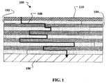
本発明の実施形態は、無機/有機ハイブリッドバリアナノラミネートフィルムと該フィルムを形成する方法に関する。図1に概略的に示されるフィルム100は一般的には、有機材料102と無機材料104の層が交互に積層された複数の層を含む。無機層102及び有機層104の厚みは、約0.1nm乃至約1nm、約1nm乃至約10nm又は約1nm乃至約100nmである。無機層102はケイ酸塩であり得るが、その他の無機材料は以下に記載されるような適切なアルコキシドから形成され得る。バリアフィルム100は無機層102と有機層104の数、厚み及び組成を適切に選択することによりほぼ透明に形成され得る。明瞭にするために図1においては比較的少数の層からなるものが示されているが、典型的なデバイスのためのバリアフィルムは、例えば数千のような更に多数の層を有する。 Embodiments of the present invention relate to inorganic / organic hybrid barrier nanolaminate films and methods of forming the films. The
有機層104は、例えば、ポリエチレンナフタレート(PEN)、ポリエーテルエーテルケトン(PEEK)又はポリエーテルスルホン(PES)のようなポリマーである。加えて、スチレンポリマー前駆体、メチルスチレンポリマー前駆体、(メタ)アクリレートポリマー前駆体、これら前駆体のフッ素化及び非フッ素化形の両方及びこれらの前駆体の二つ以上の組み合わせから創製されるポリマーは有機層104として使用され得る。これらの有機材料はそれらの優れた熱的特性及び優れたガスバリア特性から望ましい。更に、例えば、最上層110のような一つ以上の有機層104は選択的にフルオロアルキルシランのような超撥水層であり得る。フルオロアルキルシランの薄膜は、例えば、アキラナカジマ(Akira Nakajima)らによる「自己洗浄特性を備えた透明な超撥水薄膜(Transparent Superhydrophobic Thin Films with Self−Cleaning Properties」、ラングミュア(Langmuir)2000、第16巻、7044−7047頁、に記載されており、当該刊行物は本明細書において参照により援用される。 The
バリアフィルム100の層構造は、経路108により示されるような層の界面にて、水又は酸素が、例えばピンホール及び/又は間隙を介して該バリアフィルムを貫通してその下層側にある基質106まで到達するための長い経路を提供する。ナノラミネートバリアフィルム100の酸素及び水蒸気に対する透過性は層の数を変更することにより調整され得る。バリアフィルム100内において数百乃至数千の無機層102及び有機層104が互いにかみ合ったものを用いることにより、ナノラミネート内にランダムに配置されたピンホールと組み合わせられた多数の層は、水蒸気及び酸素のような分子がバリアフィルム100の外側にある環境から進入するための曲がりくねった経路を形成する。層が多くなれば多くなるほど、分子を透過させるための経路がより曲がりくねったものになる。従って、層が多くなれば多くなるほど、水蒸気及び酸素に対するバリアフィルム100の透過性は小さくなる。本発明の実施形態において、複合バリアフィルム100には、100以上、1000以上、10000以上、100000以上又はそれ以上の個々の層が存在している。 The layer structure of the
更に、得られた有機層104の疎水性を調整(増大及び/又は低減)して、該バリアフィルム100の透過性を調整するために、有機層104を形成するために使用されるポリマー前駆体には疎水基が組み込まれるか、或いは該疎水基が取り除かれる。例えば、それらに限定されるものではないがメチル基及びベンジル(芳香族)基のような非極性の疎水基がポリマー前駆体に結合される。一般的に、イオン強度が増大すると、疎水的な相互作用は増大する。例えば、以下に記載されるアニオン及びカチオンは、非常に好ましい疎水性相互作用を示すものから疎水性相互作用を低減させるものという順序にて列挙されている。 In addition, the polymer precursor used to form the
アニオン:PO43−、SO42−、CH3COO−、Cl−、Br−、NO−、ClO4−、I−、SCn−。
カチオン:NH4+、Rb+、K+、Na+、Cs+、Li+、Mg2+、Ca2+、Ba2+。Anions: PO43− , SO42− , CH3 COO− , Cl− , Br− , NO− , ClO4− , I− , SCn− .
Cations: NH4+ , Rb+ , K+ , Na+ , Cs+ , Li+ , Mg2+ , Ca2+ , Ba2+ .
これらのアニオン及び/又はカチオン及び/又は類似の化合物の任意のものがポリマー前駆体に組み込まれ、疎水性の調整されたポリマーが得られる。
加えて、トリプトファン、イソロイシン、フェニルアラニン、チロシン、ロイシン、バリン、メチオニン、及びアラニンのような疎水性アミノ酸がポリマー前駆体の側鎖として使用され得る。Any of these anions and / or cations and / or similar compounds are incorporated into the polymer precursor to obtain a hydrophobically tuned polymer.
In addition, hydrophobic amino acids such as tryptophan, isoleucine, phenylalanine, tyrosine, leucine, valine, methionine, and alanine can be used as the side chain of the polymer precursor.
更に、ジェミニ型界面活性剤(又は、二本鎖型界面活性剤と称される)は非常に反応性に富み、構造指向剤として使用される。ジェミニ型界面活性剤は、分子中に二つの親水性の頭部基と二つの疎水基とを有し、単一の親水基と単一の疎水基とのみを有する従来の界面活性剤とは相異なる。 In addition, gemini surfactants (or referred to as double-stranded surfactants) are very reactive and are used as structure directing agents. A gemini-type surfactant has two hydrophilic head groups and two hydrophobic groups in the molecule, and is different from conventional surfactants having only a single hydrophilic group and a single hydrophobic group. Different.
層の数及び組成を適切に選択することにより、バリアフィルム100の酸素透過性は、約1cc/m2/日、0.1cc/m2/日、0.01cc/m2/日、10−3cc/m2/日、10−4cc/m2/日、10−5cc/m2/日、10−6cc/m2/日、又は10−7cc/m2/日未満に形成され得る。同様に、バリアフィルム100の水蒸気透過性は、約1g/m2/日、0.1g/m2/日、0.01g/m2/日、10−3g/m2/日、10−4g/m2/日、10−5g/m2/日、10−6g/m2/日、又は10−7g/m2/日未満に形成され得る。By appropriately selecting the number and composition of layers, the oxygen permeability of the
ナノラミネートバリアフィルム100は、ゾル−ゲル法を用いた自己集合による単一の工程(又は、少数の連続工程)からなる方法により形成される。ゾル−ゲル法を用いたナノ複合材料の自己集合は、例えばブリンカ(Brinker)らによる米国特許第6264741号明細書に記載されており、当該特許の全体が参照により援用される。概して、ゾルは、一つ以上のアルコキシド、アルコール、水及び希塩酸(HCl)を混合し、得られた混合物を加熱することにより調製される。次に、カップリング剤が該混合物に加えられ、次に界面活性剤(又はジェミニ型界面活性剤)が加えられるが、当該界面活性剤の初期濃度が臨界ミセル濃度未満となるのに十分な量にて加えられる。次に、例えばPEN、PEEK、又はPESの形成に適したモノマーのような一つ以上のポリマー前駆体が加えられ、次に架橋剤及び反応開始剤が加えられる。代替的に、ポリマー前駆体は、スチレンポリマー前駆体、メチルスチレンポリマー前駆体、(メタ)アクリレートポリマー前駆体、これら前駆体のフッ素化及び非フッ素化形のいずれか及びこれらの前駆体の二つ以上の組み合わせを含む。基質はゾルでコーティングされ、アルコールが蒸発される。アルコールの蒸発により自己集合反応を引き起こし、図1に関して記載された多層バリア構造を形成する。 The
適切なアルコキシドは、中心元素Xの周囲に構造化される。適切な中心元素Xは、Al、B、Ba、Pb、Se、Si及びSnを含む。その他の適切な中心元素Xは、例えば、Ag、Au、Cd、Co、Cr、Cu、Fe、Ir、Mn、Mo、Nb、Ni、Sr、Ta、Ti、V、W、Y、Zn、Zr等のような遷移元素を含む。例えば、シリコン(Si)ベースの無機層102に対して、適切なアルコキシドの例としては、テトラエチルオルトシリケート(TEOS)のようなポリシロキサンを含む。例えば、チタニウム(Ti)ベースの無機層102に対して、適切なアルコキシドの例としては、チタニウムエトキシド又はチタニウムイソプロポキシドを含む。 Suitable alkoxides are structured around the central element X. Suitable central elements X include Al, B, Ba, Pb, Se, Si and Sn. Other suitable central elements X are, for example, Ag, Au, Cd, Co, Cr, Cu, Fe, Ir, Mn, Mo, Nb, Ni, Sr, Ta, Ti, V, W, Y, Zn, Zr Transition elements such as and the like. For example, for a silicon (Si) based
ゾルの調製及び調整
一般性を失うことのない一例として、ゾルは、例えば、テトラエチルオルトシリケート(Si(OCH2CH3)4、又はTEOSとして知られている)、エタノール、水及び希塩酸(シロキサンの凝縮速度を最小限とするために希釈される)とをそれぞれ1:3.8:1:5×10−5のモル比にて混合し、約60℃にて約90分間加熱することにより調製される。次にゾルは1:2の比率にてエタノールを用いて希釈され、次に水及び希塩酸が加えられる。7−オクテニルトリメトキシシラン(OTS)、又はメタクリルオキシプロピルトリメトキシシラン(MPS)のようなカップリング剤が混合物に加えられ、セチルトリメチルアンモニウムブロマイド(CTAB)のような界面活性剤が加えられる。その際、界面活性剤の初期濃度は臨界ミセル濃度未満である。約一時間撹拌した後に、モノマー(例えば、2,6−ジメチルナフタレン(DMN:ポリエチレンナフタレート(PEN)を生成するために)、又はビスフェノールA及びジ−パラ−フルオロフェニルスルホン(B/FS、ポリエーテルスルホン(PES)を形成するために)のような一組のモノマーが次に加えられ、架橋剤(ヘキサンジオールジメタクリレート(HDM)のような)及び反応開始剤が加えられる。紫外線開始剤であるベンゾインジメチルエーテル(BME)が加えられ得る。熱的開始剤として、1,1’−アゾビス(1−シクロヘキサンカルボニトリル)(ACHN)が使用され得る。Preparation and preparation of sols As an example without losing generality, the sols are, for example, tetraethylorthosilicate (known as Si (OCH2 CH3 )4 , or TEOS), ethanol, water and dilute hydrochloric acid (of siloxanes). Prepared in a molar ratio of 1: 3.8: 1: 5 × 10⁻⁵ respectively and heated at about 60 ° C. for about 90 minutes. Is done. The sol is then diluted with ethanol at a ratio of 1: 2 and then water and dilute hydrochloric acid are added. A coupling agent such as 7-octenyltrimethoxysilane (OTS) or methacryloxypropyltrimethoxysilane (MPS) is added to the mixture, and a surfactant such as cetyltrimethylammonium bromide (CTAB) is added. In that case, the initial concentration of the surfactant is less than the critical micelle concentration. After stirring for about one hour, a monomer (e.g., 2,6-dimethylnaphthalene (DMN: To produce polyethylene naphthalate (PEN)), orbisphenol A and di - p - fluorophenyl sulfone (B / FS A set of monomers (such as to form polyethersulfone (PES)) is then added, followed by a crosslinker (such as hexanediol dimethacrylate (HDM)) and an initiator. The agent benzoin dimethyl ether (BME) can be added, and 1,1′-azobis (1-cyclohexanecarbonitrile) (ACHN) can be used as a thermal initiator.
ゾルの化学的性質を調整するために、界面活性剤、水、エタノール、TEOS、及び有機モノマーの濃度が変更され得る。フィルムを約125℃−150℃又はそれ以上(及び/又は有機材料の分解温度未満)にてアニーリングすることにより更に、シロキサン材料が緻密化され、不透過性が改善される。In order to adjust the sol chemistry, the concentrations of surfactant, water, ethanol, TEOS, and organic monomers can be varied. Further by annealing atfull Irumu about 125 ° C. -150 ° C. or more (and / or below the decomposition temperature of the organic material), a siloxane material is densified, impermeability is improved.
コーティング及びナノラミネートの自己集合
基質106は、例えばディップコーティング、スピンコーティング、噴霧コーティング、ウェブコーティング又はマイクログラビアウェブコーティングのような任意の適切な技術によりゾル混合物を用いてコーティングされる。適切なコーティング機は、例えば、ファウステル(Faustel)社(ウィスコンシン州、ジャーマンタウンに所在)から市販されている。特に、ベルナーマチス社(Werner Mathis AG)(スイス国、チューリッヒ所在)から得られる連続コータ・タイプBAがゾル混合物を基質にコーティングするために使用され得る。約1ミクロンから10ミクロンまで、100ミクロンまでの湿式層にてゾルが基質にコーティングされることが好ましい。例えば、約100ミクロンから約1ミリメートルの厚みのようなより厚い湿式層もまた使用され得る。バリアフィルム100は真空装置を使用することなく製造され得るので、当該工程は非常に簡単であり、比較的低コストである。Coating and Nanolaminate Self-
一例として、基質は、例えば、ディップコーティング(例えば、広い面積の基質に対して25cm/分の浸漬及び引き上げ速度)又はスピンコーティング(例えば、小さい面積の基質に対して約1500rpmにて約1分間)によりゾルを用いて迅速にコーティングされ得る。コーティング後、ゾルのエタノール成分は蒸発し始め、水及び界面活性剤の濃度の増大により該界面活性剤の濃度が臨界ミセル濃度を超え、ミセルの形成と、アルコール可溶性有機モノマーのミセル内部への取り込みを生ずる。このTEOS及びCTABをベースとしたゾルゲル化学がナノ構造体の自己集合を提供し、その化学的骨格は緻密かつ安定な材料に凝縮する。 By way of example, the substrate can be, for example, dip coating (eg, 25 cm / min dipping and lifting speeds for large area substrates) or spin coating (eg, about 1 minute at about 1500 rpm for small area substrates). Can be rapidly coated with a sol. After coating, the ethanol component of the sol begins to evaporate, the concentration of the surfactant exceeds the critical micelle concentration by increasing the concentration of water and surfactant, the formation of micelles, and the incorporation of alcohol-soluble organic monomers into the micelles Is produced. This sol-gel chemistry based on TEOS and CTAB provides nanostructure self-assembly, and its chemical skeleton is condensed into a dense and stable material.
蒸発により誘導される分配は、発生し、かつ出現したゾルゲルのシロキサン骨格構造にわたり有機成分及び無機成分の両方の共分散を促進するための手段を提供する。エタノールが蒸発し続けられると、シリカ−界面活性剤−モノマーのミセルは、約10秒という時間尺度にて界面が有機化されたリオトロピック液晶中間層に自己集合する。交互に存在する界面層の有機材料のポリマー化は紫外線又は熱のいずれかにより誘導され、ポリマー化された無機シロキサンの骨格構造を安定化する。多数フィルムにおける得られたナノ複合構造は、(a)有機ポリマー化、(b)無機ポリマー化、及び(c)有機界面の共有結合により安定化される。単一のコーティング工程は、各々が約1nmの厚みである個々の層からなる少なくとも1000nmの厚みのフィルムを生成する。材料の自己集合の性質を巧みに利用することにより、各組が1000の層からなるものがわずか数秒で形成される。得られるバリアフィルムにおけるより多くの数の層は、コーティングと蒸発の連続を複数回繰り返すことにより、及び/又はより厚いコーティングを堆積させることにより得られる。 Distribution induced by evaporation provides a means for promoting the co-dispersion of both organic and inorganic components across the siloxane skeleton structure of the generated and emerging sol-gel. As the ethanol continues to evaporate, the silica-surfactant-monomer micelles self-assemble into a lyotropic liquid crystal interlayer whose interface is organized on a time scale of about 10 seconds. Alternating interfacial organic material polymerisation is induced by either UV or heat to stabilize the polymerized inorganic siloxane backbone structure. The resulting nanocomposite structure in multiple films is stabilized by (a) organic polymerisation, (b) inorganic polymerisation, and (c) covalent bonding at the organic interface. A single coating process produces a film with a thickness of at least 1000 nm consisting of individual layers, each about 1 nm thick. By exploiting the self-assembling nature of materials, each set consists of 1000 layers in just a few seconds. A greater number of layers in the resulting barrier film can be obtained by repeating the coating and evaporation sequence several times and / or by depositing a thicker coating.
オプション及び代替的な実施形態
上述のタイプのコンフォーマルな又は非コンフォーマルなナノラミネートバリアコーティングは、種々の平坦な、及び平坦でない表面に、二次元及び三次元にて塗布される。より詳細には、このナノラミネートのアプローチは、光電子デバイス(例えば、LED、太陽電池、FET、レーザ)、製薬製品(パッケージ内の錠剤等)、医療用装置、食品(包装された食品、飲料、キャンディ)、ディスプレイスクリーン(タッチパネルディスプレイ、フラットパネルディスプレイ)、エレクトロルミネッセントなウィンドウ及びその他のウェインドウ及び透明なフィルム及びコーティング、電子部品並びに厳しい環境にて使用される電化製品のシャーシを封入及び/又は保護するために使用され得る。Options and Alternative Embodiments Conformal or non-conformal nanolaminate barrier coatings of the type described above are applied in two and three dimensions to a variety of flat and non-planar surfaces. More specifically, this nanolaminate approach includes optoelectronic devices (eg, LEDs, solar cells, FETs, lasers), pharmaceutical products (tablets in packages, etc.), medical devices, foods (packaged foods, beverages, Candy), display screens (touch panel displays, flat panel displays), electroluminescent windows and other windows and transparent films and coatings, electronic components and appliance chassis used in harsh environments and / or Or it can be used to protect.
更に、染料又は顔料をフィルムに組み込むことにより、ナノラミネートは着色され、種々の光電子デバイスにおける光学フィルタとしての使用に提供される。
上述の記載は、本発明のより好ましい実施形態の完全な記載であるが、種々の代替物、変更物及び等価物を使用することも可能である。従って、本発明の範囲は上述の詳細な記載を参照することにより決定されるべきではなく、代わりに、添付された特許請求の範囲を、その等価物の完全な範囲とともに参照して決定されるべきである。添付された請求の範囲は、ミーンズプラスファンクションの限定が、「を意味する」なる記載を用いた所定の請求項に明瞭に引用されていない限り、該限定を含むものとして解釈されるべきではない。Furthermore, by incorporating dyes or pigments into the film, the nanolaminate is colored and provided for use as an optical filter in a variety of optoelectronic devices.
While the above is a complete description of the more preferred embodiments of the invention, various alternatives, modifications and equivalents may be used. Accordingly, the scope of the invention should not be determined by reference to the above detailed description, but instead should be determined by reference to the appended claims along with their full scope of equivalents. Should. The appended claims should not be construed to include such limitations unless the means plus function limitation is expressly recited in a given claim with the meaning "meaning". .
Claims (10)
Translated fromJapaneseアルコキシドと、アルコールと、水と、希塩酸とを混合して、得られた混合物を加熱する工程と、
前記混合物にカップリング剤を加える工程と、
前記混合物に、その初期濃度を臨界ミセル濃度未満とするのに十分な量である界面活性剤を加える工程と、
前記混合物に、ポリエチレンナフタレート、ポリエーテルエーテルケトン又はポリエーテルスルホンの形成に適したポリマー前駆体、フッ素化又は非フッ素化スチレンポリマー前駆体、フッ素化又は非フッ素化メチルスチレンポリマー前駆体、フッ素化又は非フッ素化(メタ)アクリレートポリマー前駆体及びこれらの前駆体の二つ以上の組み合わせ及び誘導体の少なくとも一方、からなる群より選択された一つ以上のポリマー前駆体を加える工程と、
架橋剤及び反応開始剤を前記混合物に加える工程と、
前記混合物で基質をコーティングする工程と、
ゾルが有機ポリマー層と無機層が交互に積層されたバリアフィルムにより特徴付けられる自己集合構造を形成するべく前記アルコールを蒸発させる工程と、を含み、
前記方法は、前記フィルムの有機材料のうちの最も低い分解温度未満である温度にて該フィルムをアニーリングする工程を更に含み、
前記有機ポリマー層の二つ以上が超撥水材料を含む、方法。In a method for forming an inorganic / organic hybrid nanolaminate barrier film, the method comprises:
Mixing the alkoxide, alcohol, water and dilute hydrochloric acid, and heating the resulting mixture;
Adding a coupling agent to the mixture;
Adding to the mixture a surfactant in an amount sufficient to bring its initial concentration below the critical micelle concentration;
The mixture includesa polymer precursor suitable for the formation of polyethylene naphthalate, polyetheretherketoneor polyethersulfone, fluorinated or non-fluorinated styrene polymer precursor, fluorinated or non-fluorinated methylstyrene polymer precursor, fluorinated Or addingone or more polymer precursors selected from the group consisting of non-fluorinated (meth) acrylate polymer precursors and / or combinations and derivatives of two or more of these precursors;
Adding a crosslinking agent and a reaction initiator to the mixture;
Coating a substrate with the mixture;
Evaporating the alcohol to form aself-assembled structure characterized by abarrier film in which the sol is alternately laminated with organic polymer layers and inorganic layers;
The methodfurtherlook including the step of annealing the film Tebefore Symbol organic materialssac Chinotemperature less than the lowest decomposition temperature of thefilm,
The method wherein two or more of the organic polymer layers comprise a super water repellent material .
Applications Claiming Priority (3)
| Application Number | Priority Date | Filing Date | Title |
|---|---|---|---|
| US10/698,988US8722160B2 (en) | 2003-10-31 | 2003-10-31 | Inorganic/organic hybrid nanolaminate barrier film |
| US10/698,988 | 2003-10-31 | ||
| PCT/US2004/034993WO2005044551A1 (en) | 2003-10-31 | 2004-10-18 | Inorganic/organic hybrid nanolaminate barrier film |
Related Child Applications (1)
| Application Number | Title | Priority Date | Filing Date |
|---|---|---|---|
| JP2013185134ADivisionJP2013256132A (en) | 2003-10-31 | 2013-09-06 | Inorganic/organic hybrid nanolaminate barrier film |
Publications (2)
| Publication Number | Publication Date |
|---|---|
| JP2007533430A JP2007533430A (en) | 2007-11-22 |
| JP5703431B2true JP5703431B2 (en) | 2015-04-22 |
Family
ID=34550810
Family Applications (2)
| Application Number | Title | Priority Date | Filing Date |
|---|---|---|---|
| JP2006538120AExpired - Fee RelatedJP5703431B2 (en) | 2003-10-31 | 2004-10-18 | Method for forming inorganic / organic hybrid nanolaminate barrier film |
| JP2013185134APendingJP2013256132A (en) | 2003-10-31 | 2013-09-06 | Inorganic/organic hybrid nanolaminate barrier film |
Family Applications After (1)
| Application Number | Title | Priority Date | Filing Date |
|---|---|---|---|
| JP2013185134APendingJP2013256132A (en) | 2003-10-31 | 2013-09-06 | Inorganic/organic hybrid nanolaminate barrier film |
Country Status (5)
| Country | Link |
|---|---|
| US (2) | US8722160B2 (en) |
| EP (1) | EP1682339A4 (en) |
| JP (2) | JP5703431B2 (en) |
| TW (1) | TWI376825B (en) |
| WO (1) | WO2005044551A1 (en) |
Cited By (1)
| Publication number | Priority date | Publication date | Assignee | Title |
|---|---|---|---|---|
| US9983751B2 (en) | 2015-11-20 | 2018-05-29 | Samsung Display Co., Ltd | Touch sensing unit, display device and fabrication method of the touch sensing unit |
Families Citing this family (66)
| Publication number | Priority date | Publication date | Assignee | Title |
|---|---|---|---|---|
| US6623861B2 (en) | 2001-04-16 | 2003-09-23 | Battelle Memorial Institute | Multilayer plastic substrates |
| US6866901B2 (en) | 1999-10-25 | 2005-03-15 | Vitex Systems, Inc. | Method for edge sealing barrier films |
| US20100330748A1 (en) | 1999-10-25 | 2010-12-30 | Xi Chu | Method of encapsulating an environmentally sensitive device |
| US8900366B2 (en) | 2002-04-15 | 2014-12-02 | Samsung Display Co., Ltd. | Apparatus for depositing a multilayer coating on discrete sheets |
| US8808457B2 (en) | 2002-04-15 | 2014-08-19 | Samsung Display Co., Ltd. | Apparatus for depositing a multilayer coating on discrete sheets |
| US7510913B2 (en) | 2003-04-11 | 2009-03-31 | Vitex Systems, Inc. | Method of making an encapsulated plasma sensitive device |
| US20050271893A1 (en)* | 2004-06-04 | 2005-12-08 | Applied Microstructures, Inc. | Controlled vapor deposition of multilayered coatings adhered by an oxide layer |
| US8722160B2 (en)* | 2003-10-31 | 2014-05-13 | Aeris Capital Sustainable Ip Ltd. | Inorganic/organic hybrid nanolaminate barrier film |
| US7227066B1 (en)* | 2004-04-21 | 2007-06-05 | Nanosolar, Inc. | Polycrystalline optoelectronic devices based on templating technique |
| WO2005121397A2 (en)* | 2004-06-04 | 2005-12-22 | Applied Microstructures, Inc. | Controlled vapor deposition of multilayered coatings adhered by an oxide layer |
| US7879396B2 (en)* | 2004-06-04 | 2011-02-01 | Applied Microstructures, Inc. | High aspect ratio performance coatings for biological microfluidics |
| US20090032108A1 (en)* | 2007-03-30 | 2009-02-05 | Craig Leidholm | Formation of photovoltaic absorber layers on foil substrates |
| US7838868B2 (en)* | 2005-01-20 | 2010-11-23 | Nanosolar, Inc. | Optoelectronic architecture having compound conducting substrate |
| US7772487B1 (en) | 2004-10-16 | 2010-08-10 | Nanosolar, Inc. | Photovoltaic cell with enhanced energy transfer |
| US8927315B1 (en) | 2005-01-20 | 2015-01-06 | Aeris Capital Sustainable Ip Ltd. | High-throughput assembly of series interconnected solar cells |
| KR20060124940A (en)* | 2005-06-01 | 2006-12-06 | 삼성전자주식회사 | Manufacturing Method of Flexible Display |
| US20070005024A1 (en)* | 2005-06-10 | 2007-01-04 | Jan Weber | Medical devices having superhydrophobic surfaces, superhydrophilic surfaces, or both |
| US7767498B2 (en) | 2005-08-25 | 2010-08-03 | Vitex Systems, Inc. | Encapsulated devices and method of making |
| US8084685B2 (en)* | 2006-01-12 | 2011-12-27 | Heliovolt Corporation | Apparatus for making controlled segregated phase domain structures |
| US20070160763A1 (en)* | 2006-01-12 | 2007-07-12 | Stanbery Billy J | Methods of making controlled segregated phase domain structures |
| US7767904B2 (en)* | 2006-01-12 | 2010-08-03 | Heliovolt Corporation | Compositions including controlled segregated phase domain structures |
| US7943846B2 (en)* | 2006-04-21 | 2011-05-17 | Innovalight, Inc. | Group IV nanoparticles in an oxide matrix and devices made therefrom |
| US8158450B1 (en)* | 2006-05-05 | 2012-04-17 | Nanosolar, Inc. | Barrier films and high throughput manufacturing processes for photovoltaic devices |
| KR100763933B1 (en) | 2006-07-11 | 2007-10-05 | 인하대학교 산학협력단 | Process for preparing organic-inorganic hybrid material |
| US8088502B2 (en)* | 2006-09-20 | 2012-01-03 | Battelle Memorial Institute | Nanostructured thin film optical coatings |
| US8034317B2 (en) | 2007-06-18 | 2011-10-11 | Heliovolt Corporation | Assemblies of anisotropic nanoparticles |
| WO2009042660A1 (en)* | 2007-09-24 | 2009-04-02 | Qspex Technologies, Inc. | Method for manufacturing polarized ophthalmic lenses |
| JP2009221541A (en)* | 2008-03-17 | 2009-10-01 | Fujifilm Corp | Vacuum film formation method for inorganic layer, barrier laminate, device, and optical component |
| US20100031997A1 (en)* | 2008-08-11 | 2010-02-11 | Basol Bulent M | Flexible thin film photovoltaic modules and manufacturing the same |
| US8389050B2 (en)* | 2008-11-21 | 2013-03-05 | Corning Incorporated | Method of coating tubes using a self-assembly process |
| US9073287B2 (en)* | 2008-12-15 | 2015-07-07 | Industrial Technology Research Insititute | Organic/inorganic multi-layered gas barrier film |
| US9184410B2 (en) | 2008-12-22 | 2015-11-10 | Samsung Display Co., Ltd. | Encapsulated white OLEDs having enhanced optical output |
| US9337446B2 (en) | 2008-12-22 | 2016-05-10 | Samsung Display Co., Ltd. | Encapsulated RGB OLEDs having enhanced optical output |
| EP2393955A4 (en)* | 2009-02-04 | 2015-04-22 | Heliovolt Corp | METHOD FOR MANUFACTURING TRANSPARENT CONDUCTIVE OXIDE FILM CONTAINING INDIUM, METALLIC TARGETS USED IN THE METHOD, AND PHOTOVOLTAIC DEVICES USING THE SAME |
| FR2956869B1 (en) | 2010-03-01 | 2014-05-16 | Alex Hr Roustaei | SYSTEM FOR PRODUCING HIGH CAPACITY FLEXIBLE FILM FOR PHOTOVOLTAIC AND OLED CELLS BY CYCLIC LAYER DEPOSITION |
| US8418418B2 (en) | 2009-04-29 | 2013-04-16 | 3Form, Inc. | Architectural panels with organic photovoltaic interlayers and methods of forming the same |
| TW201040299A (en)* | 2009-05-05 | 2010-11-16 | Fraunhofer Ges Forschung | Layer system having barrier properties and a structured conductive layer, method for producing the same, and use of such a layer system |
| CA2708193A1 (en)* | 2009-06-05 | 2010-12-05 | Heliovolt Corporation | Process for synthesizing a thin film or composition layer via non-contact pressure containment |
| TWI391886B (en)* | 2009-06-12 | 2013-04-01 | Au Optronics Corp | Flexible touch display apparatus |
| US8256621B2 (en)* | 2009-09-11 | 2012-09-04 | Pro-Pak Industries, Inc. | Load tray and method for unitizing a palletized load |
| US8590338B2 (en) | 2009-12-31 | 2013-11-26 | Samsung Mobile Display Co., Ltd. | Evaporator with internal restriction |
| US8021641B2 (en)* | 2010-02-04 | 2011-09-20 | Alliance For Sustainable Energy, Llc | Methods of making copper selenium precursor compositions with a targeted copper selenide content and precursor compositions and thin films resulting therefrom |
| WO2011146115A1 (en) | 2010-05-21 | 2011-11-24 | Heliovolt Corporation | Liquid precursor for deposition of copper selenide and method of preparing the same |
| WO2012023973A2 (en) | 2010-08-16 | 2012-02-23 | Heliovolt Corporation | Liquid precursor for deposition of indium selenide and method of preparing the same |
| KR101844557B1 (en)* | 2011-02-08 | 2018-04-02 | 어플라이드 머티어리얼스, 인코포레이티드 | Method for hybrid encapsulation of an organic light emitting diode |
| CN103563246A (en)* | 2011-04-01 | 2014-02-05 | 纳沃萨恩公司 | Roof panel-like photovoltaic modules |
| KR101891987B1 (en)* | 2011-05-31 | 2018-08-28 | 엘지디스플레이 주식회사 | Organic Light Emitting Device and Method for manufacturing the same |
| DE102011056761A1 (en) | 2011-12-21 | 2013-08-08 | Leibniz-Institut Für Neue Materialien Gemeinnützige Gmbh | Pigmented, finely structured tribological composite material |
| WO2013091685A1 (en) | 2011-12-21 | 2013-06-27 | Leibniz-Institut Für Neue Materialien Gemeinnützige Gmbh | Highly structured composite material and process for the manufacture of protective coatings for corroding substrates |
| US20140370217A1 (en) | 2011-12-21 | 2014-12-18 | Tenaris Connections Limited | Corrosion Resistant Equipment for Oil and/or Gas Applications |
| CN103374138A (en)* | 2012-04-25 | 2013-10-30 | 深圳富泰宏精密工业有限公司 | Shell and preparation method thereof |
| US9105797B2 (en) | 2012-05-31 | 2015-08-11 | Alliance For Sustainable Energy, Llc | Liquid precursor inks for deposition of In—Se, Ga—Se and In—Ga—Se |
| US9112275B2 (en)* | 2012-09-05 | 2015-08-18 | Raytheon Company | Radome film |
| CN104037352A (en)* | 2013-03-07 | 2014-09-10 | 海洋王照明科技股份有限公司 | Organic light emission diode and preparation method thereof |
| JP2015069508A (en)* | 2013-09-30 | 2015-04-13 | 凸版印刷株式会社 | Touch panel |
| JP6946185B2 (en)* | 2014-11-17 | 2021-10-06 | セイジ・エレクトロクロミクス,インコーポレイテッド | Multiple barrier layer sealed laminate |
| WO2016138195A1 (en) | 2015-02-25 | 2016-09-01 | Corning Incorporated | Optical structures and articles with multilayer stacks having high hardness and methods for making the same |
| CN107502003B (en)* | 2016-06-14 | 2020-06-02 | 中国科学院理化技术研究所 | Preparation method of hydrophobic inorganic powder material |
| KR102127463B1 (en)* | 2017-08-18 | 2020-06-29 | 한국과학기술원 | Encapsulation structure for transparent flexible organic electronic device |
| US10529951B2 (en) | 2017-08-18 | 2020-01-07 | Korea Advanced Institute Of Science And Technology | Encapsulation structure for transparent flexible organic electronic device |
| CN108054289B (en)* | 2017-12-15 | 2020-03-06 | 京东方科技集团股份有限公司 | A package component and its manufacturing method, and a display device |
| KR102578827B1 (en) | 2018-04-24 | 2023-09-15 | 삼성전자주식회사 | Flexible organic-inorganic passivation layer an method of fabricating the same |
| CN109950418A (en)* | 2019-03-18 | 2019-06-28 | 云谷(固安)科技有限公司 | Display panel and display screen |
| CN109888128A (en)* | 2019-03-25 | 2019-06-14 | 京东方科技集团股份有限公司 | OLED display panel packaging method and display panel manufacturing method |
| KR102417793B1 (en)* | 2020-12-15 | 2022-07-14 | 포항공과대학교 산학협력단 | Composition for an organic-inorganic hybrid gas barrier film containing a fluorine-based precursor and amphiphilic legged structured polymeric alkoxysilane precursor and a gas barrier film using the same |
| CN117812931B (en)* | 2023-12-27 | 2025-02-11 | 惠科股份有限公司 | Method for manufacturing display panel, display panel and display device |
Family Cites Families (23)
| Publication number | Priority date | Publication date | Assignee | Title |
|---|---|---|---|---|
| JPS5947987B2 (en)* | 1979-10-08 | 1984-11-22 | 富士写真フイルム株式会社 | Matsuto film that can be added/edited |
| DE3884435T2 (en)* | 1987-03-25 | 1994-02-17 | Hitachi Ltd | Processes for producing high-purity water and process for using this water. |
| DE3725338A1 (en)* | 1987-07-30 | 1989-02-09 | Nukem Gmbh | ENCLOSURE OF A PHOTOVOLTAIC ELEMENT |
| CA2060294C (en)* | 1991-02-06 | 2000-01-18 | Kazufumi Ogawa | Chemically absorbed film and method of manufacturing the same |
| JPH07270615A (en) | 1994-03-31 | 1995-10-20 | Central Glass Co Ltd | Holographic laminated body |
| US5554670A (en)* | 1994-09-12 | 1996-09-10 | Cornell Research Foundation, Inc. | Method of preparing layered silicate-epoxy nanocomposites |
| US5746631A (en)* | 1996-01-11 | 1998-05-05 | Mccarthy; Peter T. | High efficiency hydrofoil and swim fin designs |
| US6057035A (en)* | 1997-06-06 | 2000-05-02 | Triton Systems, Inc. | High-temperature polymer/inorganic nanocomposites |
| JPH11135820A (en)* | 1997-08-27 | 1999-05-21 | Canon Inc | Solar cell module and reinforcing member for solar cell module |
| US6146225A (en) | 1998-07-30 | 2000-11-14 | Agilent Technologies, Inc. | Transparent, flexible permeability barrier for organic electroluminescent devices |
| US6264741B1 (en)* | 1998-11-25 | 2001-07-24 | Sandia Corporation | Self-assembly of nanocomposite materials |
| US6818163B1 (en)* | 1999-02-12 | 2004-11-16 | Dow Global Technologies Inc. | Nanocomposite articles and process for making |
| WO2000078540A1 (en)* | 1999-06-17 | 2000-12-28 | Triton Systems, Inc. | High performance nanocomposites |
| US6472467B1 (en)* | 1999-10-21 | 2002-10-29 | Dow Global Technologies Inc. | Inorganic/organic compositions |
| US6413645B1 (en) | 2000-04-20 | 2002-07-02 | Battelle Memorial Institute | Ultrabarrier substrates |
| US6623861B2 (en) | 2001-04-16 | 2003-09-23 | Battelle Memorial Institute | Multilayer plastic substrates |
| US6573652B1 (en) | 1999-10-25 | 2003-06-03 | Battelle Memorial Institute | Encapsulated display devices |
| US6866901B2 (en)* | 1999-10-25 | 2005-03-15 | Vitex Systems, Inc. | Method for edge sealing barrier films |
| TW490997B (en)* | 2000-03-31 | 2002-06-11 | Seiko Epson Corp | Method of manufacturing organic EL element, and organic EL element |
| CA2404013A1 (en)* | 2000-04-21 | 2001-11-01 | Hongyou Fan | Prototyping of patterned functional nanostructures |
| DE60127527T2 (en)* | 2001-01-19 | 2007-12-13 | 3M Innovative Properties Co., St. Paul | Water-soluble or water-dispersible fluorochemical silanes to make substrates oil and water repellent |
| US20040168627A1 (en)* | 2003-02-27 | 2004-09-02 | Sharp Laboratories Of America, Inc. | Atomic layer deposition of oxide film |
| US8722160B2 (en)* | 2003-10-31 | 2014-05-13 | Aeris Capital Sustainable Ip Ltd. | Inorganic/organic hybrid nanolaminate barrier film |
- 2003
- 2003-10-31USUS10/698,988patent/US8722160B2/ennot_activeExpired - Fee Related
- 2004
- 2004-10-18EPEP04796054Apatent/EP1682339A4/ennot_activeWithdrawn
- 2004-10-18JPJP2006538120Apatent/JP5703431B2/ennot_activeExpired - Fee Related
- 2004-10-18TWTW093131587Apatent/TWI376825B/enactive
- 2004-10-18WOPCT/US2004/034993patent/WO2005044551A1/enactiveApplication Filing
- 2013
- 2013-09-06JPJP2013185134Apatent/JP2013256132A/enactivePending
- 2014
- 2014-05-09USUS14/274,527patent/US20140314958A1/ennot_activeAbandoned
Cited By (1)
| Publication number | Priority date | Publication date | Assignee | Title |
|---|---|---|---|---|
| US9983751B2 (en) | 2015-11-20 | 2018-05-29 | Samsung Display Co., Ltd | Touch sensing unit, display device and fabrication method of the touch sensing unit |
Also Published As
| Publication number | Publication date |
|---|---|
| EP1682339A1 (en) | 2006-07-26 |
| US20050095422A1 (en) | 2005-05-05 |
| US20140314958A1 (en) | 2014-10-23 |
| US8722160B2 (en) | 2014-05-13 |
| WO2005044551A1 (en) | 2005-05-19 |
| TWI376825B (en) | 2012-11-11 |
| TW200520275A (en) | 2005-06-16 |
| EP1682339A4 (en) | 2010-08-11 |
| JP2007533430A (en) | 2007-11-22 |
| JP2013256132A (en) | 2013-12-26 |
Similar Documents
| Publication | Publication Date | Title |
|---|---|---|
| JP5703431B2 (en) | Method for forming inorganic / organic hybrid nanolaminate barrier film | |
| TWI252325B (en) | Plastic substrate having multi-layer structure and method for preparing the same | |
| TWI491501B (en) | Gas barrier laminated film | |
| KR101013370B1 (en) | Gas barrier laminated film | |
| CA2084045C (en) | Metal oxide film having minutely roughed surface and method of forming same on glass substrate | |
| KR101762299B1 (en) | High-barrier composites and method for the production thereof | |
| US20100112270A1 (en) | Multilayer film, method for manufacture thereof and articles including the same | |
| US20060154048A1 (en) | Article having functional coating film thereon, method for manufacture thereof, and applying material for forming functional coating film | |
| TW201119858A (en) | Gas-barrier laminated film | |
| JP2017526971A (en) | Alternate laminated textured multilayer laminate transfer film | |
| JP4205241B2 (en) | Laminated body | |
| JP4104383B2 (en) | Transparent water vapor barrier film and method for producing the same | |
| JP2007210262A (en) | Transparent barrier film and method for producing the same | |
| CN104870386A (en) | Transparent substrate, in particular a glass substrate, coated with at least one at least bifunctional porous layer, manufacturing method and uses thereof | |
| JP2004082598A (en) | Gas barrier laminate and method of manufacturing the same | |
| KR101557497B1 (en) | Thin film having a gradient of material composition and method of manufacturing the same | |
| CN101065240B (en) | Gas barrier laminated film | |
| JP4097947B2 (en) | Transparent water vapor barrier film | |
| JP3933894B2 (en) | Transparent water vapor barrier film | |
| KR20160106388A (en) | Composition for forming a barrier layer, and a barrier layer obtained therefrom | |
| KR102325601B1 (en) | A method for preparing a fluorinated composite, a fluorinated composite prepared therefrom, and a barrier layer comprising the same | |
| JP4974557B2 (en) | Retort processing paper container | |
| JP2021088116A (en) | Laminate film for display element protection, quantum dot laminate and backlight unit | |
| JP2009132059A (en) | Gas barrier vapor deposition film, method for producing the same, and laminate material using the same | |
| JP5151037B2 (en) | Transparent barrier film and method for producing the same |
Legal Events
| Date | Code | Title | Description |
|---|---|---|---|
| A621 | Written request for application examination | Free format text:JAPANESE INTERMEDIATE CODE: A621 Effective date:20071009 | |
| A977 | Report on retrieval | Free format text:JAPANESE INTERMEDIATE CODE: A971007 Effective date:20100728 | |
| A131 | Notification of reasons for refusal | Free format text:JAPANESE INTERMEDIATE CODE: A131 Effective date:20100817 | |
| A601 | Written request for extension of time | Free format text:JAPANESE INTERMEDIATE CODE: A601 Effective date:20101117 | |
| A602 | Written permission of extension of time | Free format text:JAPANESE INTERMEDIATE CODE: A602 Effective date:20101125 | |
| A521 | Request for written amendment filed | Free format text:JAPANESE INTERMEDIATE CODE: A523 Effective date:20110216 | |
| A131 | Notification of reasons for refusal | Free format text:JAPANESE INTERMEDIATE CODE: A131 Effective date:20120104 | |
| A601 | Written request for extension of time | Free format text:JAPANESE INTERMEDIATE CODE: A601 Effective date:20120404 | |
| A602 | Written permission of extension of time | Free format text:JAPANESE INTERMEDIATE CODE: A602 Effective date:20120411 | |
| A521 | Request for written amendment filed | Free format text:JAPANESE INTERMEDIATE CODE: A523 Effective date:20120704 | |
| A02 | Decision of refusal | Free format text:JAPANESE INTERMEDIATE CODE: A02 Effective date:20130507 | |
| A521 | Request for written amendment filed | Free format text:JAPANESE INTERMEDIATE CODE: A523 Effective date:20130906 | |
| A911 | Transfer to examiner for re-examination before appeal (zenchi) | Free format text:JAPANESE INTERMEDIATE CODE: A911 Effective date:20131101 | |
| A01 | Written decision to grant a patent or to grant a registration (utility model) | Free format text:JAPANESE INTERMEDIATE CODE: A01 Effective date:20131224 | |
| A61 | First payment of annual fees (during grant procedure) | Free format text:JAPANESE INTERMEDIATE CODE: A61 Effective date:20140122 | |
| R150 | Certificate of patent or registration of utility model | Ref document number:5703431 Country of ref document:JP Free format text:JAPANESE INTERMEDIATE CODE: R150 | |
| LAPS | Cancellation because of no payment of annual fees |