JP5701014B2 - Method for manufacturing ejection element substrate - Google Patents
Method for manufacturing ejection element substrateDownload PDFInfo
- Publication number
- JP5701014B2 JP5701014B2JP2010248886AJP2010248886AJP5701014B2JP 5701014 B2JP5701014 B2JP 5701014B2JP 2010248886 AJP2010248886 AJP 2010248886AJP 2010248886 AJP2010248886 AJP 2010248886AJP 5701014 B2JP5701014 B2JP 5701014B2
- Authority
- JP
- Japan
- Prior art keywords
- element substrate
- supply port
- manufacturing
- protective film
- resin
- Prior art date
- Legal status (The legal status is an assumption and is not a legal conclusion. Google has not performed a legal analysis and makes no representation as to the accuracy of the status listed.)
- Expired - Fee Related
Links
Images

Classifications
- B—PERFORMING OPERATIONS; TRANSPORTING
- B41—PRINTING; LINING MACHINES; TYPEWRITERS; STAMPS
- B41J—TYPEWRITERS; SELECTIVE PRINTING MECHANISMS, i.e. MECHANISMS PRINTING OTHERWISE THAN FROM A FORME; CORRECTION OF TYPOGRAPHICAL ERRORS
- B41J2/00—Typewriters or selective printing mechanisms characterised by the printing or marking process for which they are designed
- B41J2/005—Typewriters or selective printing mechanisms characterised by the printing or marking process for which they are designed characterised by bringing liquid or particles selectively into contact with a printing material
- B41J2/01—Ink jet
- B41J2/135—Nozzles
- B41J2/16—Production of nozzles
- B41J2/1621—Manufacturing processes
- B41J2/1626—Manufacturing processes etching
- B41J2/1628—Manufacturing processes etching dry etching
- B—PERFORMING OPERATIONS; TRANSPORTING
- B41—PRINTING; LINING MACHINES; TYPEWRITERS; STAMPS
- B41J—TYPEWRITERS; SELECTIVE PRINTING MECHANISMS, i.e. MECHANISMS PRINTING OTHERWISE THAN FROM A FORME; CORRECTION OF TYPOGRAPHICAL ERRORS
- B41J2/00—Typewriters or selective printing mechanisms characterised by the printing or marking process for which they are designed
- B41J2/005—Typewriters or selective printing mechanisms characterised by the printing or marking process for which they are designed characterised by bringing liquid or particles selectively into contact with a printing material
- B41J2/01—Ink jet
- B41J2/135—Nozzles
- B41J2/16—Production of nozzles
- B41J2/1601—Production of bubble jet print heads
- B41J2/1603—Production of bubble jet print heads of the front shooter type
- B—PERFORMING OPERATIONS; TRANSPORTING
- B41—PRINTING; LINING MACHINES; TYPEWRITERS; STAMPS
- B41J—TYPEWRITERS; SELECTIVE PRINTING MECHANISMS, i.e. MECHANISMS PRINTING OTHERWISE THAN FROM A FORME; CORRECTION OF TYPOGRAPHICAL ERRORS
- B41J2/00—Typewriters or selective printing mechanisms characterised by the printing or marking process for which they are designed
- B41J2/005—Typewriters or selective printing mechanisms characterised by the printing or marking process for which they are designed characterised by bringing liquid or particles selectively into contact with a printing material
- B41J2/01—Ink jet
- B41J2/135—Nozzles
- B41J2/16—Production of nozzles
- B41J2/1621—Manufacturing processes
- B41J2/1626—Manufacturing processes etching
- B41J2/1629—Manufacturing processes etching wet etching
- B—PERFORMING OPERATIONS; TRANSPORTING
- B41—PRINTING; LINING MACHINES; TYPEWRITERS; STAMPS
- B41J—TYPEWRITERS; SELECTIVE PRINTING MECHANISMS, i.e. MECHANISMS PRINTING OTHERWISE THAN FROM A FORME; CORRECTION OF TYPOGRAPHICAL ERRORS
- B41J2/00—Typewriters or selective printing mechanisms characterised by the printing or marking process for which they are designed
- B41J2/005—Typewriters or selective printing mechanisms characterised by the printing or marking process for which they are designed characterised by bringing liquid or particles selectively into contact with a printing material
- B41J2/01—Ink jet
- B41J2/135—Nozzles
- B41J2/16—Production of nozzles
- B41J2/1621—Manufacturing processes
- B41J2/1631—Manufacturing processes photolithography
- B—PERFORMING OPERATIONS; TRANSPORTING
- B41—PRINTING; LINING MACHINES; TYPEWRITERS; STAMPS
- B41J—TYPEWRITERS; SELECTIVE PRINTING MECHANISMS, i.e. MECHANISMS PRINTING OTHERWISE THAN FROM A FORME; CORRECTION OF TYPOGRAPHICAL ERRORS
- B41J2/00—Typewriters or selective printing mechanisms characterised by the printing or marking process for which they are designed
- B41J2/005—Typewriters or selective printing mechanisms characterised by the printing or marking process for which they are designed characterised by bringing liquid or particles selectively into contact with a printing material
- B41J2/01—Ink jet
- B41J2/135—Nozzles
- B41J2/16—Production of nozzles
- B41J2/1621—Manufacturing processes
- B41J2/1632—Manufacturing processes machining
- B41J2/1634—Manufacturing processes machining laser machining
- B—PERFORMING OPERATIONS; TRANSPORTING
- B41—PRINTING; LINING MACHINES; TYPEWRITERS; STAMPS
- B41J—TYPEWRITERS; SELECTIVE PRINTING MECHANISMS, i.e. MECHANISMS PRINTING OTHERWISE THAN FROM A FORME; CORRECTION OF TYPOGRAPHICAL ERRORS
- B41J2/00—Typewriters or selective printing mechanisms characterised by the printing or marking process for which they are designed
- B41J2/005—Typewriters or selective printing mechanisms characterised by the printing or marking process for which they are designed characterised by bringing liquid or particles selectively into contact with a printing material
- B41J2/01—Ink jet
- B41J2/135—Nozzles
- B41J2/16—Production of nozzles
- B41J2/1621—Manufacturing processes
- B41J2/1637—Manufacturing processes molding
- B41J2/1639—Manufacturing processes molding sacrificial molding
- B—PERFORMING OPERATIONS; TRANSPORTING
- B41—PRINTING; LINING MACHINES; TYPEWRITERS; STAMPS
- B41J—TYPEWRITERS; SELECTIVE PRINTING MECHANISMS, i.e. MECHANISMS PRINTING OTHERWISE THAN FROM A FORME; CORRECTION OF TYPOGRAPHICAL ERRORS
- B41J2/00—Typewriters or selective printing mechanisms characterised by the printing or marking process for which they are designed
- B41J2/005—Typewriters or selective printing mechanisms characterised by the printing or marking process for which they are designed characterised by bringing liquid or particles selectively into contact with a printing material
- B41J2/01—Ink jet
- B41J2/135—Nozzles
- B41J2/16—Production of nozzles
- B41J2/1621—Manufacturing processes
- B41J2/164—Manufacturing processes thin film formation
- B41J2/1642—Manufacturing processes thin film formation thin film formation by CVD [chemical vapor deposition]
- B—PERFORMING OPERATIONS; TRANSPORTING
- B41—PRINTING; LINING MACHINES; TYPEWRITERS; STAMPS
- B41J—TYPEWRITERS; SELECTIVE PRINTING MECHANISMS, i.e. MECHANISMS PRINTING OTHERWISE THAN FROM A FORME; CORRECTION OF TYPOGRAPHICAL ERRORS
- B41J2/00—Typewriters or selective printing mechanisms characterised by the printing or marking process for which they are designed
- B41J2/005—Typewriters or selective printing mechanisms characterised by the printing or marking process for which they are designed characterised by bringing liquid or particles selectively into contact with a printing material
- B41J2/01—Ink jet
- B41J2/135—Nozzles
- B41J2/16—Production of nozzles
- B41J2/1621—Manufacturing processes
- B41J2/164—Manufacturing processes thin film formation
- B41J2/1643—Manufacturing processes thin film formation thin film formation by plating
- B—PERFORMING OPERATIONS; TRANSPORTING
- B41—PRINTING; LINING MACHINES; TYPEWRITERS; STAMPS
- B41J—TYPEWRITERS; SELECTIVE PRINTING MECHANISMS, i.e. MECHANISMS PRINTING OTHERWISE THAN FROM A FORME; CORRECTION OF TYPOGRAPHICAL ERRORS
- B41J2/00—Typewriters or selective printing mechanisms characterised by the printing or marking process for which they are designed
- B41J2/005—Typewriters or selective printing mechanisms characterised by the printing or marking process for which they are designed characterised by bringing liquid or particles selectively into contact with a printing material
- B41J2/01—Ink jet
- B41J2/135—Nozzles
- B41J2/16—Production of nozzles
- B41J2/1621—Manufacturing processes
- B41J2/164—Manufacturing processes thin film formation
- B41J2/1645—Manufacturing processes thin film formation thin film formation by spincoating
- B—PERFORMING OPERATIONS; TRANSPORTING
- B41—PRINTING; LINING MACHINES; TYPEWRITERS; STAMPS
- B41J—TYPEWRITERS; SELECTIVE PRINTING MECHANISMS, i.e. MECHANISMS PRINTING OTHERWISE THAN FROM A FORME; CORRECTION OF TYPOGRAPHICAL ERRORS
- B41J2/00—Typewriters or selective printing mechanisms characterised by the printing or marking process for which they are designed
- B41J2/005—Typewriters or selective printing mechanisms characterised by the printing or marking process for which they are designed characterised by bringing liquid or particles selectively into contact with a printing material
- B41J2/01—Ink jet
- B41J2/135—Nozzles
- B41J2/14—Structure thereof only for on-demand ink jet heads
- B41J2002/14403—Structure thereof only for on-demand ink jet heads including a filter
Landscapes
- Engineering & Computer Science (AREA)
- Manufacturing & Machinery (AREA)
- Physics & Mathematics (AREA)
- Optics & Photonics (AREA)
- Particle Formation And Scattering Control In Inkjet Printers (AREA)
Description
Translated fromJapanese本発明は、液体を吐出する吐出素子基板の製造方法に関する。 The present invention relates to a method for manufacturing an ejection element substrate that ejects liquid.
一般に、インクジェット記録ヘッドの吐出素子基板は、インクを吐出する吐出口と、吐出素子基板にインクを供給するインク供給口と、インク供給口及び吐出口に連通するインク流路と、を基本構造として有する。 In general, an ejection element substrate of an ink jet recording head has, as a basic structure, an ejection port that ejects ink, an ink supply port that supplies ink to the ejection element substrate, and an ink flow path that communicates with the ink supply port and the ejection port. Have.
吐出素子基板の製造にはポイントになる部分がいくつかある。そのポイントの1つは型材を用いてインク流路を形成する点である。また、そのポイントの1つは、基板をエッチングして貫通孔としてのインク供給口を形成する点である。 There are several parts that are important in the manufacture of the discharge element substrate. One of the points is that an ink flow path is formed using a mold material. One of the points is that the substrate is etched to form an ink supply port as a through hole.
インク供給口はインクと接するためインクに対する耐性を確保する必要がある。そのため、表面の結晶方位が(100)面のシリコン基板に結晶異方性エッチングを用いてインク供給口を形成する方法が用いられている。しかし、この方法ではシリコン基板の平面に対して54.7°という角度をなすインク供給口が形成されるため、インク供給口の開口幅が大きくなってしまう場合がある。 Since the ink supply port contacts the ink, it is necessary to ensure resistance to the ink. Therefore, a method is used in which an ink supply port is formed on a silicon substrate having a surface crystal orientation of (100) plane using crystal anisotropic etching. However, in this method, since the ink supply port is formed at an angle of 54.7 ° with respect to the plane of the silicon substrate, the opening width of the ink supply port may be increased.
このインク耐性とインク供給口幅の問題を解決する方法として、特許文献1に記載されるように、供給口をDeep−RIE法を用いて形成し、供給口内部に保護膜を形成する方法が提案されている。 As a method for solving the problems of the ink resistance and the ink supply port width, as described in
また、インクジェット記録ヘッドは、近年、高画質化の要求に対して小液滴化を実現する手段が提案されており、特許文献に記載されるように、フィルタ構造を形成した形態が提案されている。 In recent years, ink jet recording heads have been proposed to realize smaller droplets in response to the demand for higher image quality. As described in patent literature, a form in which a filter structure is formed has been proposed. Yes.
インク耐性をもつ有機保護膜を内壁に有するインク供給口において基板の小型化を目指すと、特許文献1に記載のようにインク供給口の側壁を垂直に形成することが望ましい。その構造においてインク供給口にフィルタ構造をフォトリソグラフィのパターニング技術によって形成することを考えた場合、型材によってインク流路を形成している観点から、インク供給口は裏面から形成することになり、インク供給口の位置精度は裏面基準になることが一般的である。 In order to reduce the size of the substrate at the ink supply port having an organic protective film having ink resistance on the inner wall, it is desirable to form the side wall of the ink supply port vertically as described in
しかしながら、特許文献2のようなフィルタ構造は、表面側からのパターニングによって形成されるため、裏面基準のインク供給口と合わせる形となり、高精度にお互いを位置合わせし難い場合がある。 However, since the filter structure as in
そのため、高精度にフィルタ構造を形成するためには、裏面から形成されるインク供給口の形状に合わせて同様に裏面からフィルタ構造をパターニングすることが望ましい。しかし、その場合、高アスペクト比の形状に対するパターニングとなるため、フォトリソグラフィによるパターニングでは、段差部に有利なスプレー塗布法を用いたとしても、側壁部にレジストが塗布できず、カバレージ不良が発生する場合がある。また、底部はレジストが溜まり易くなるため、レジストは規定膜厚より厚くなり、パターニング不良が発生する場合がある。また、露光においても、焦点深度の高い等倍露光を用いてもフォーカス合わせが困難であり、段差部の不要な反射が発生し、露光不良となる場合がある。 Therefore, in order to form the filter structure with high accuracy, it is desirable that the filter structure is similarly patterned from the back surface according to the shape of the ink supply port formed from the back surface. However, in this case, since the patterning is performed for a shape with a high aspect ratio, even if a spray coating method that is advantageous for the stepped portion is used in the patterning by photolithography, the resist cannot be applied to the side wall portion, resulting in poor coverage. There is a case. In addition, since the resist tends to accumulate at the bottom, the resist becomes thicker than the specified film thickness, and patterning defects may occur. In addition, in the exposure, even if the same-size exposure with a high depth of focus is used, focusing is difficult, and unnecessary reflection of the stepped portion may occur, resulting in an exposure failure.
そこで、本発明の目的は、基板内を貫通する供給口の底部にフィルタ構造を精度良く形成できる吐出素子基板の製造方法を提供することである。 SUMMARY OF THE INVENTION An object of the present invention is to provide a method for manufacturing a discharge element substrate that can accurately form a filter structure at the bottom of a supply port that penetrates the substrate.
本発明は、
液体を吐出する吐出口及び該吐出口に連通する液体流路を有する流路形成部材と、前記液体流路に前記液体を供給する供給口を有する基板と、を備え、前記供給口の底部にフィルタ構造を有する吐出素子基板の製造方法であって、
(1)前記基板の前記流路形成部材が配置される側の第一の面と反対側の第二の面から反応性イオンエッチングを行って貫通口を形成することにより前記供給口を形成する工程と、
(2)前記供給口の側面及び底部に樹脂保護膜を配置する工程と、
(3)前記供給口の底部の前記樹脂保護膜に前記第二の面側からのレーザー加工によって微細口を形成する工程と、
を有することを特徴とする吐出素子基板の製造方法である。The present invention
A flow path forming member having a discharge port for discharging liquid and a liquid flow channel communicating with the discharge port; and a substrate having a supply port for supplying the liquid to the liquid flow channel, and provided at the bottom of the supply port A method for manufacturing a discharge element substrate having a filter structure,
(1) The supply port is formed by performing reactive ion etching from a second surface opposite to the first surface on the side where the flow path forming member of the substrate is disposed to form a through hole. Process,
(2) a step of disposing a resin protective film on the side and bottom of the supply port;
(3) forming a fine mouth by laser processing from the second surface side in the resin protective film at the bottom of the supply port;
It is a manufacturing method of the discharge element board | substrate characterized by having.
本発明によれば、高画質化を達成すためのフィルタ構造を精度良く形成することができ、吐出素子基板の小型化を図ることができる。 According to the present invention, a filter structure for achieving high image quality can be formed with high accuracy, and the ejection element substrate can be miniaturized.
本発明は、液体を吐出する吐出口及び該吐出口に連通する液体流路を有する流路形成部材と、前記液体流路に前記液体を供給する供給口を有する基板と、を備え、前記供給口の底部にフィルタ構造を有する吐出素子基板の製造方法に関する。 The present invention comprises a flow path forming member having a discharge port for discharging a liquid and a liquid flow path communicating with the discharge port, and a substrate having a supply port for supplying the liquid to the liquid flow path, The present invention relates to a method for manufacturing a discharge element substrate having a filter structure at the bottom of a mouth.
まず、基板の流路形成部材が配置される側の第一の面と反対側の第二の面から反応性イオンエッチングを行って貫通口を形成することにより前記供給口を形成する。 First, the supply port is formed by performing reactive ion etching from the second surface opposite to the first surface on the side where the flow path forming member of the substrate is disposed to form a through hole.
次に、供給口の側面及び底部に樹脂保護膜を配置する。この際、CVD法を用いて樹脂保護膜を形成することが好ましい。 Next, a resin protective film is disposed on the side and bottom of the supply port. At this time, it is preferable to form a resin protective film using a CVD method.
次に、供給口の底部の樹脂保護膜に第二の面側からのレーザー加工によって微細口を形成する。 Next, a fine port is formed in the resin protective film at the bottom of the supply port by laser processing from the second surface side.
以上の工程により、供給口の底部にフィルタ構造を有する吐出素子基板を精度良く形成することができる。 Through the above steps, an ejection element substrate having a filter structure at the bottom of the supply port can be accurately formed.
また、基板としては、第一の面に表面層を有するものを用いることができる。該表面層は、基板の表面側に形成される層を指し、特に制限されるものではない。表面層としては、例えば、後述するように、液体流路の型材や層間絶縁膜、導電層等が挙げられる。 As the substrate, a substrate having a surface layer on the first surface can be used. The surface layer refers to a layer formed on the surface side of the substrate, and is not particularly limited. Examples of the surface layer include a liquid channel mold material, an interlayer insulating film, and a conductive layer, as will be described later.
表面層を有する基板を用いる場合、第二の面から反応性イオンエッチングを表面層に到達するまで行うことにより、基板に供給口を形成することができる。続いて、供給口の側面及び供給口の底部に露出する表面層に樹脂保護膜を形成し、供給口の底部の樹脂保護膜に微細口を形成することにより、フィルタ構造を形成すればよい。 When a substrate having a surface layer is used, a supply port can be formed in the substrate by performing reactive ion etching from the second surface until reaching the surface layer. Subsequently, the filter structure may be formed by forming a resin protective film on the side surface of the supply port and the surface layer exposed on the bottom of the supply port, and forming a fine port in the resin protective film on the bottom of the supply port.
以下、本発明について実施形態や実施例を用いて説明する。なお、以下の説明では、本発明の適用例としてインクジェット記録ヘッドを例に挙げて説明するが、本発明の適用範囲はこれに限定されるものではなく、バイオッチップ作製や電子回路印刷用途の液体吐出ヘッド等にも適用できる。液体吐出ヘッドとしては、インクジェット記録ヘッドの他にも、例えばカラーフィルター製造用ヘッド等も挙げられる。 The present invention will be described below with reference to embodiments and examples. In the following description, an inkjet recording head will be described as an example of application of the present invention. However, the scope of application of the present invention is not limited to this, and liquid ejection for biochip manufacturing and electronic circuit printing applications is described. It can be applied to a head or the like. As the liquid discharge head, in addition to the ink jet recording head, for example, a head for producing a color filter can be cited.
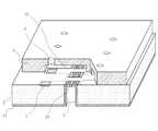
図1は本発明の製造方法によって得られる吐出素子基板の構成例を示す概略斜視図である。図1において、吐出素子基板はインクの吐出口を上向きに示している。なお、本明細書において、吐出口が形成される面側を上側とし、その反対側、つまりインク供給口が形成される面側を下側とする。 FIG. 1 is a schematic perspective view showing a configuration example of a discharge element substrate obtained by the manufacturing method of the present invention. In FIG. 1, the ejection element substrate shows an ink ejection port facing upward. In this specification, the surface side on which the ejection ports are formed is referred to as the upper side, and the opposite side, that is, the surface side on which the ink supply ports are formed is referred to as the lower side.
図1において、吐出素子基板は、基板2と、該基板2の上に形成された流路形成部材3とからなる。流路形成部材3は、上面にインク吐出口4を有し、該インク吐出口4に連通するインク流路25を基板2とともに構成する。基板2は、インク流路25にインクを供給するための貫通孔としてインク供給口5を有する。インク供給口5の側壁は基板面にほぼ垂直に形成されている。インク供給口5の流路形成部材3が配置される側の開口には微細口を有する樹脂部材21が配置され、この微細口を有する樹脂部材21がフィルタとして機能し、インクに含まれる不純物を除去することができる。樹脂部材21は、インク供給口5の側壁及び基板2の裏面にも配置されている。なお、本明細書において、基板2の吐出素子基板が配置される側の面を表面(第一の面とも称す)とし、基板2の吐出素子基板が配置される側の面と反対側の面を裏面(第二の面とも称す)とする。 In FIG. 1, the ejection element substrate includes a
吐出素子基板を備えるインクジェット記録ヘッドは、エネルギー発生素子1から発生したエネルギーによってインクをインク吐出口4から吐出し、記録媒体に着弾させることにより印字を行う。インクはインク供給口5から吐出素子基板内に流入し、インク流路25を通過し、インク吐出口4に到達する。 An ink jet recording head provided with an ejection element substrate performs printing by ejecting ink from an
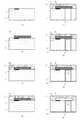
図2は、本実施形態の吐出素子基板の製造方法を説明するための工程断面図である。以下、図2を参照して本実施形態の吐出素子基板の製造方法について説明する。 FIG. 2 is a process cross-sectional view for explaining the method for manufacturing the ejection element substrate of the present embodiment. Hereinafter, a method for manufacturing the ejection element substrate of this embodiment will be described with reference to FIG.
まず、図2(a)に示すように、エネルギー発生素子1を有する基板2を用意する。 First, as shown in FIG. 2A, a
具体的には、シリコン基板2上に一般的な半導体デバイス工程と同じように半導体素子を作り込み、フォトリソグラフィを用いた多層配線技術によってエネルギー発生素子1を形成することにより、基板2を得ることができる。 Specifically, a semiconductor element is formed on a
次に、図2(b)に示すように、上述の表面層としてのインク流路の型材24を形成する。この型材24は最終的には除去されるため、除去を前提とした材料を選択する。 Next, as shown in FIG. 2B, the above-described ink
次に、図2(c)に示すように、型材24の上に流路形成部材3を塗布する。 Next, as shown in FIG. 2C, the flow
次に、図2(d)に示すように、流路形成部材3にフォトリソグラフィによりインク吐出口4を形成する。 Next, as shown in FIG. 2D,
次に、図2(e)に示すように、基板2の裏面からのRIE(反応性イオンエッチング)法によりインク供給口5を形成する。RIE法は、Boschプロセスを用いたDeep−RIE法であることが望ましい。インク供給口5は、基板を貫通して形成される。 Next, as illustrated in FIG. 2E, the
次に、図2(f)に示すように、インク供給口5の側面及び底面を含む基板2裏面全体に樹脂保護膜21を形成する。樹脂保護膜21の形成方法は、有機CVDを用いることができる。この樹脂保護膜21により、インク供給口5に良好な耐インク性を付与することができる。 Next, as shown in FIG. 2F, a resin
樹脂保護膜は、ポリパラキシリレン、ポリモノクロロパラキシリレン、ポリジクロロパラキシリレン、ポリテトラフルオロパラキシリレン、及びポリパラキシリレン誘導体等を含むポリパラキシリレン樹脂、ポリ尿素樹脂、並びにポリイミド樹脂からなる群から選ばれる少なくとも1種を用いてCVD法により形成することが好ましい。これにより、アスペクト比が高い供給口の側面や底部に良好に樹脂膜を形成することができる。 The resin protective film includes polyparaxylylene resin, polymonochloroparaxylylene, polydichloroparaxylylene, polytetrafluoroparaxylylene, polyparaxylylene derivatives, polyparaxylylene resin, polyurea resin, and polyimide. It is preferable to form by CVD method using at least 1 sort (s) chosen from the group which consists of resin. Thereby, it is possible to satisfactorily form the resin film on the side surface or bottom of the supply port having a high aspect ratio.
次に、図2(g)に示すように、インク供給口5の底部にフィルタ構造を形成するために、インク供給口5の底部に形成された樹脂保護膜21にレーザーにより穴(微細口)23を形成する。 Next, as shown in FIG. 2G, in order to form a filter structure at the bottom of the
このときのレーザー加工としては、樹脂保護膜21のみを選択的に除去する直接描画によるパターニングを用いることができる。 As the laser processing at this time, patterning by direct drawing for selectively removing only the resin
そして、図2(h)に示すように、型材24を溶解除去し、インク流路25を形成する。 Then, as shown in FIG. 2 (h), the
以上の方法により供給口の底部にフィルタ構造を有する吐出素子基板を作製することができる。 By the above method, an ejection element substrate having a filter structure at the bottom of the supply port can be produced.
以下、本発明について実施例を参照にして説明する。なお、本発明は以下の実施例に限定されるものではない。 Hereinafter, the present invention will be described with reference to examples. In addition, this invention is not limited to a following example.
(実施例1)
図2は、第1の実施形態の吐出素子基板の製造方法の一例を示す図である。以下、図2に従って説明する。Example 1
FIG. 2 is a diagram illustrating an example of a method for manufacturing the ejection element substrate according to the first embodiment. Hereinafter, a description will be given with reference to FIG.
図2(a)に示すように、厚さ200μmのシリコン基板にヒータを形成し、エネルギー発生素子1を有する基板2を用意した。 As shown in FIG. 2A, a heater was formed on a silicon substrate having a thickness of 200 μm, and a
次に、図2(b)に示すように、金めっき法により型材24を形成した。 Next, as shown in FIG. 2B, a
次に、図2(c)に示すように、カチオン重合型エポキシ樹脂を基板2及び型材24の上にスピンコートし、流路形成部材3を形成した。 Next, as shown in FIG. 2 (c), a cationic polymerization type epoxy resin was spin-coated on the
次に、図2(d)に示すように、露光、現像工程により流路形成部材3にインク吐出口4を形成した。 Next, as shown in FIG. 2D,
次に、図2(e)に示すように、エッチングガスとしてSF6ガスとC4F8ガスを用い、エッチングと成膜を交互に行うDeep−RIEにより、基板2の裏面からインク供給口5を形成した。Next, as shown in FIG. 2 (e), using the SF6 gas and C4 F8 gas as an etching gas, the Deep-RIE to etch and deposition alternately, the ink supply port from the rear surface of the
次に、図2(f)に示すように、有機CVDを用い、厚さ2μmのポリパラキシリレンからなる樹脂保護膜21をインク供給口の側面及び底面を含む基板裏面に成膜した。 Next, as shown in FIG. 2F, a resin
有機CVD膜はつきまわりが良好であり、高アスペクト比のインク供給口(基板厚さ:200μm、開口寸法:50×50μm)においても良好なカバレージ性を実現する。 The organic CVD film has good throwing power and realizes good coverage even at a high aspect ratio ink supply port (substrate thickness: 200 μm, opening size: 50 × 50 μm).
次に、図2(g)に示すように、樹脂保護膜21をインク供給口5のフィルタ構造を形成するように、1つのインク供給口の底部に4つのレーザー加工により穴(微細口)23を形成した。 Next, as shown in FIG. 2G, the resin
このレーザー加工において、1μs以下のパルスレーザーを用いることが好ましい。このようなレーザーを用いることにより、検討の結果、樹脂保護膜を除去して形成した穴の形状をシャープで良好にでき、かつレーザーが型材24に対してダメージを与えずに選択的に穴を形成できることを確認した。さらに、このような観点から、可視光より短い波長のレーザーを用いることが好ましい。つまり、レーザー加工において、1μs以下のパルスレーザーであって、波長が可視光より短いレーザーを用いることが好ましい。より具体的には、1μs以下のパルスレーザーである。ポリパラキシリレンを加工する場合は、380nm以下の波長であり、特に波長200〜270nmの光を使用するのがよい。 In this laser processing, it is preferable to use a pulse laser of 1 μs or less. By using such a laser, as a result of investigation, the shape of the hole formed by removing the resin protective film can be made sharp and good, and the laser can selectively open the hole without damaging the
本実施例では、紫外線パルスレーザーであるエキシマレーザー(波長:248nm,パルス幅:30ns、エネルギー密度:0.6J/cm2)を用いてφ10μmの微細口を形成した。この時、樹脂保護膜21の膜厚は2μmであり、レーザー照射のショット数を重ねて所望の樹脂膜厚を除去した。In this example, an excimer laser (wavelength: 248 nm, pulse width: 30 ns, energy density: 0.6 J / cm2 ), which is an ultraviolet pulse laser, was used to form a fine aperture of φ10 μm. At this time, the film thickness of the resin
次に、図2(h)に示すように、予め形成していた金めっきの型材24をよう素とよう化カリウムを含むエッチング液を用いて溶解除去し、インク流路25を形成した。 Next, as shown in FIG. 2 (h), the gold
以上の方法により、吐出素子基板を作製した。 A discharge element substrate was produced by the above method.
(実施例2)
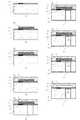
図3は、第2実施形態の吐出素子基板の製造方法の一例を示す図である。以下、図3に従って説明する。(Example 2)
FIG. 3 is a diagram illustrating an example of a method for manufacturing a discharge element substrate according to the second embodiment. Hereinafter, a description will be given with reference to FIG.
図3(a)に示すように、厚さ200μmのシリコン基板にヒータを形成し、エネルギー発生素子1を形成した。また、同時に、基板2に多層配線層の層間絶縁膜13と、多層配線層の上部保護膜12をプラズマCVDにより成膜し形成した。層間絶縁膜13は厚さ1μmのシリコン酸化膜であり、上部保護膜12は厚さ0.5μmのシリコン窒化膜である。本実施例において、層間絶縁膜が上述の表面層となる。 As shown in FIG. 3A, a heater was formed on a silicon substrate having a thickness of 200 μm, and the
層間絶縁膜としては、例えば、シリコン酸化物、シリコン窒化物、及びシリコン炭化物からなる群から選ばれる少なくとも1種を含んで構成される。 The interlayer insulating film includes, for example, at least one selected from the group consisting of silicon oxide, silicon nitride, and silicon carbide.
次に、図3(b)に示すように、型材24を形成した。その方法としては、溶解可能な樹脂であるポリメチルイソプロペニルケトン(東京応化工業(株)社製、商品名;ODUR−1010)をスピンコートし、露光、現像によりパターニングし型材24を形成した。 Next, a
次に、図3(c)に示すように、カチオン重合型エポキシ樹脂を基板2及び型材24の上にスピンコートし、流路形成部材3を形成した。 Next, as shown in FIG. 3C, a cationic polymerization type epoxy resin was spin coated on the
次に、図3(d)に示すように、露光、現像工程により流路形成部材3にインク吐出口4を形成した。 Next, as shown in FIG. 3D,
次に、図3(e)に示すように、エッチングガスとしてSF6ガスとC4F8ガスを用い、エッチングと成膜を交互に行うDeep−RIE法により、基板2の裏面からインク供給口5を形成した。Next, as shown in FIG. 3E, an ink supply port is formed from the back surface of the
エッチングは、層間絶縁膜13を残して止めた。ここでは、シリコン基板とシリコン酸化膜の部材差を利用してエッチングを止めた。 Etching was stopped leaving the
次に、図3(f)に示すように、CVD法を用い、厚さ2μmのポリパラキシリレンからなる樹脂保護膜21をインク供給口5の側面及び底面を含む基板裏面全面に成膜した。 Next, as shown in FIG. 3F, a resin
有機CVD膜はつきまわりが良好であり、高アスペクト比のインク供給口(基板厚さ:200μm、開口寸法:50×50μm)においても良好なカバレージ性を実現する。 The organic CVD film has good throwing power and realizes good coverage even at a high aspect ratio ink supply port (substrate thickness: 200 μm, opening size: 50 × 50 μm).
次に、図3(g)に示すように、樹脂保護膜21にインク供給口5のフィルタ構造を形成するように、1つのインク供給口の底部にレーザー加工により4つの穴(微細口)23を形成した。 Next, as shown in FIG. 3G, four holes (fine openings) 23 are formed by laser processing at the bottom of one ink supply port so that the filter structure of the
この工程において、1μs以下のパルスレーザーであって可視光より短い波長のレーザーを用いることにより、微細口の形状がシャープであり、かつレーザーが層間絶縁膜13にダメージを与えずに樹脂保護膜を選択的に除去可能であることを確認した。 In this step, a pulse laser of 1 μs or less and a laser having a wavelength shorter than visible light is used, so that the shape of the fine mouth is sharp and the resin protective film is formed without damaging the interlayer insulating
本実施例では紫外線パルスレーザーであるエキシマレーザー(波長:248nm,パルス幅:30ns、エネルギー密度:0.6J/cm2)を用いてφ10μmの微細口を形成した。この時、樹脂保護膜21の膜厚は2μmであり、レーザー照射のショット数を重ねて所望の樹脂膜厚を除去した。In this example, an excimer laser (wavelength: 248 nm, pulse width: 30 ns, energy density: 0.6 J / cm2 ), which is an ultraviolet pulse laser, was used to form a fine aperture of φ10 μm. At this time, the film thickness of the resin
次に、図3(h)に示すように、微細口23を有する樹脂保護膜21をコンタクトマスクとして、基板裏面からCF4ガスを主としたRIE法を用いたドライエッチングにより、層間絶縁膜13及び上部保護膜12をエッチングする。エッチングは型材24まで到達し、層間絶縁膜13及び上部保護膜12に貫通穴が形成された。Next, as shown in FIG. 3H, the
次に、図3(i)に示すように、予め溶解可能な樹脂で形成していた型材24を、乳酸メチルを含むフォトレジスト剥離液を用いて溶解除去し、インク流路25を形成した。 Next, as shown in FIG. 3 (i), the
以上の方法により、吐出素子基板を作製した。 A discharge element substrate was produced by the above method.
(実施例3)
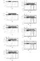
図4は、第3の実施形態の吐出素子基板の製造方法の一例を示す図である。以下、図4に従って説明するが、主に実施例2と異なる点を中心に説明する。(Example 3)
FIG. 4 is a diagram illustrating an example of a method of manufacturing a discharge element substrate according to the third embodiment. The following description will be made with reference to FIG. 4, but the description will mainly focus on differences from the second embodiment.
図4(a)〜(g)の工程は、実施例2の図3(a)〜(g)の工程と同じであり、説明を省略する。 The steps of FIGS. 4A to 4G are the same as the steps of FIGS. 3A to 3G of the second embodiment, and a description thereof will be omitted.
本実施例では、図4(h)に示すように、層間絶縁膜13と上部保護膜12の除去を、ドライエッチング法ではなく、ウエットエッチ法により行った。 In this example, as shown in FIG. 4H, the
具体的には、基板裏面からのNH4F(フッ化アンモニウム)を用いたウエットエッチングを行い、微細口23からエッチング液を侵入させることにより、層間絶縁膜13と上部保護膜12を除去した。Specifically, wet etching using NH4 F (ammonium fluoride) from the back surface of the substrate was performed, and the etchant was intruded through the
次に、図4(i)に示すように、予め溶解可能な樹脂で形成していた型材24を、乳酸メチルを含むフォトレジスト剥離液を用いて溶解除去し、インク流路25を形成した。 Next, as shown in FIG. 4 (i), the
以上の方法により、吐出素子基板を作製した。 A discharge element substrate was produced by the above method.
(実施例4)
図5は第4の実施形態の吐出素子基板の製造方法の一例を示す図である。以下、図5に従って説明する。Example 4
FIG. 5 is a diagram illustrating an example of a method of manufacturing a discharge element substrate according to the fourth embodiment. Hereinafter, a description will be given with reference to FIG.
図5(a)に示すにように、厚さ200μmのシリコン基板にヒータを形成し、エネルギー発生素子1を形成した。また、基板2の上であって供給口を形成する位置に対応する領域に、導電層14となる厚さ0.5μmのアルミニウムからなる金属薄膜を形成した。また、同時に、基板2に多層配線層の層間絶縁膜13と、多層配線層の上部保護膜12をプラズマCVDにより形成した。層間絶縁膜13は厚さ1μmのシリコン酸化膜であり、上部保護膜12は厚さ0.5μmのシリコン窒化膜である。本実施例において、導電層が上述の表面層となる。 As shown in FIG. 5A, a heater was formed on a silicon substrate having a thickness of 200 μm, and the
次に、図5(b)に示すように、型材24を形成した。その方法としては、溶解可能な樹脂であるポリメチルイソプロペニルケトン(東京応化工業(株)社製、商品名;ODUR−1010)をスピンコートし、露光、現像によりパターニングし型材24を形成した。 Next, a
次に、図5(c)に示すように、カチオン重合型エポキシ樹脂を基板2及び型材24の上にスピンコートし、流路形成部材3を形成した。 Next, as shown in FIG. 5 (c), a cationic polymerization type epoxy resin was spin-coated on the
次に、図5(d)に示すように、露光、現像工程により流路形成部材3にインク吐出口4を形成した。 Next, as shown in FIG. 5D,
次に、図5(e)に示すように、エッチングガスとしてSF6ガスとC4F8ガスを用い、エッチングと成膜を交互に行うDeep−RIE法により、基板2の裏面からインク供給口5を形成した。Next, as shown in FIG. 5E, an ink supply port is formed from the back surface of the
エッチングは、基板上の導電層14を残してエッチングを止めた。ここでは、シリコン基板と金属薄膜の部材差を利用してエッチングを止めた。 The etching was stopped leaving the
この時、導電層14はRIE法による帯電を逃がす働きをするため、Deep−RIE時に見られるノッチングの発生を抑える働きをする。導電層14としては、アルミニウム以外にも、例えば、アルミシリコン(Al/Si)、アルミ銅(Al/Cu)、アルミシリコン銅(Al/Si/Cu)などを用いることができる。 At this time, since the
次に、図5(f)に示すように、有機CVDを用い、厚さ2μmのポリパラキシリレンからなる樹脂保護膜21をインク供給口5の側面及び底面を含む基板裏面全面に成膜した。 Next, as shown in FIG. 5 (f), a resin
有機CVD膜はつきまわりが良好であり、高アスペクト比のインク供給口(基板厚さ:200μm、開口寸法:50×50μm)においても良好なカバレージ性を実現する。 The organic CVD film has good throwing power and realizes good coverage even at a high aspect ratio ink supply port (substrate thickness: 200 μm, opening size: 50 × 50 μm).
次に、図5(g)に示すように、樹脂保護膜21にインク供給口5のフィルタ構造を形成するように、1つのインク供給口の底部にレーザー加工により4つの穴23を形成した。 Next, as shown in FIG. 5G, four
この工程において、1μs以下のパルスレーザーであって可視光より短い波長のレーザーを用いることにより、微細口の形状がシャープであり、かつレーザーが導電層14にダメージを与えずに樹脂保護膜を選択的に除去可能であることを確認した。 In this process, by using a pulse laser of 1 μs or less and a wavelength shorter than visible light, the shape of the fine mouth is sharp, and the resin protective film is selected without damaging the
本実施例では紫外線パルスレーザーであるエキシマレーザー(波長:248nm,パルス幅:30ns、エネルギー密度:0.6J/cm2)を用いてφ10μmの微細口を形成した。この時、樹脂保護膜21の膜厚は2μmであり、レーザー照射のショット数を重ねて所望の樹脂膜厚を除去した。 In this example, an excimer laser (wavelength: 248 nm, pulse width: 30 ns, energy density: 0.6 J / cm 2), which is an ultraviolet pulse laser, was used to form a fine aperture of φ10 μm. At this time, the film thickness of the resin
次に、図5(h)に示すように、金属薄膜である導電層14とシリコン窒化膜である上部保護膜12を、基板裏面からNH4F(フッ化アンモニウム)を用いたウエットエッチングを行い、微細口23からエッチング液を侵入させることにより、除去した。これにより、導電層14は除去され、樹脂保護膜21だけがフィルタ構造を構成する部材として残る。図5(h)において、15は導電層がが除去された導電層除去部を示す。Next, as shown in FIG. 5H, the
次に、図5(i)に示すように、予め溶解可能な樹脂で形成していた型材24を、乳酸メチルを含むフォトレジスト剥離液を用いて溶解除去し、インク流路25を形成した。 Next, as shown in FIG. 5 (i), the
以上の方法により、吐出素子基板を作製した。 A discharge element substrate was produced by the above method.
1:エネルギー発生素子
2:基板(シリコン基板)
3:流路形成部材
4:インク吐出口
5:インク供給口
12:上部保護膜(シリコン窒化膜)
13:層間絶縁膜(シリコン酸化膜)
14:導電層
15:導電層除去部
21:樹脂保護膜
23:微細口(樹脂保護膜が除去された部分)
24:型材
25:インク流路1: Energy generating element 2: Substrate (silicon substrate)
3: flow path forming member 4: ink discharge port 5: ink supply port 12: upper protective film (silicon nitride film)
13: Interlayer insulating film (silicon oxide film)
14: Conductive layer 15: Conductive layer removal part 21: Resin protective film 23: Fine opening (part from which resin protective film has been removed)
24: Mold material 25: Ink flow path
Claims (14)
Translated fromJapanese(1)前記基板の前記流路形成部材が配置される側の第一の面と反対側の第二の面から貫通口を形成することにより前記供給口を形成する工程と、
(2)前記供給口の側面及び底部に樹脂保護膜を配置する工程と、
(3)前記供給口の底部の前記樹脂保護膜に前記第二の面側からのレーザー加工によって微細口を形成する工程と、
を有することを特徴とする吐出素子基板の製造方法。A flow path forming member having a discharge port for discharging liquid and a liquid flow channel communicating with the discharge port; and a substrate having a supply port for supplying the liquid to the liquid flow channel, and provided at the bottom of the supply port A method for manufacturing a discharge element substrate having a filter structure,
(1) forming the supply port by forming a through-hole from a second surface opposite to the first surface of the substrate on which the flow path forming member is disposed;
(2) a step of disposing a resin protective film on the side and bottom of the supply port;
(3) forming a fine mouth by laser processing from the second surface side in the resin protective film at the bottom of the supply port;
A method for manufacturing a discharge element substrate, comprising:
前記工程(2)は前記供給口の側面及び前記供給口の底部に露出する前記表面層に前記樹脂保護膜を配置する工程である請求項2または3に記載の吐出素子基板の製造方法。In the step (1), the substrate has a surface layer on the first surface, and the reactive ion etching is performed from the second surface until reaching the surface layer,
The method of manufacturing an ejection element substrate according to claim 2 or 3, wherein the step (2) is a step of disposing the resin protective film on the surface layer exposed on a side surface of the supply port and a bottom portion of the supply port.
Priority Applications (2)
| Application Number | Priority Date | Filing Date | Title |
|---|---|---|---|
| JP2010248886AJP5701014B2 (en) | 2010-11-05 | 2010-11-05 | Method for manufacturing ejection element substrate |
| US13/281,714US8691101B2 (en) | 2010-11-05 | 2011-10-26 | Method for manufacturing ejection element substrate |
Applications Claiming Priority (1)
| Application Number | Priority Date | Filing Date | Title |
|---|---|---|---|
| JP2010248886AJP5701014B2 (en) | 2010-11-05 | 2010-11-05 | Method for manufacturing ejection element substrate |
Publications (3)
| Publication Number | Publication Date |
|---|---|
| JP2012101364A JP2012101364A (en) | 2012-05-31 |
| JP2012101364A5 JP2012101364A5 (en) | 2013-12-19 |
| JP5701014B2true JP5701014B2 (en) | 2015-04-15 |
Family
ID=46018620
Family Applications (1)
| Application Number | Title | Priority Date | Filing Date |
|---|---|---|---|
| JP2010248886AExpired - Fee RelatedJP5701014B2 (en) | 2010-11-05 | 2010-11-05 | Method for manufacturing ejection element substrate |
Country Status (2)
| Country | Link |
|---|---|
| US (1) | US8691101B2 (en) |
| JP (1) | JP5701014B2 (en) |
Families Citing this family (3)
| Publication number | Priority date | Publication date | Assignee | Title |
|---|---|---|---|---|
| JP5769560B2 (en) | 2011-09-09 | 2015-08-26 | キヤノン株式会社 | Substrate for liquid discharge head and manufacturing method thereof |
| JP5935597B2 (en)* | 2012-08-25 | 2016-06-15 | 株式会社リコー | Liquid ejection head and image forming apparatus |
| JP6373013B2 (en)* | 2014-02-21 | 2018-08-15 | キヤノン株式会社 | Method for manufacturing liquid discharge head and liquid discharge head |
Family Cites Families (18)
| Publication number | Priority date | Publication date | Assignee | Title |
|---|---|---|---|---|
| US5983486A (en)* | 1995-03-10 | 1999-11-16 | Canon Kabushiki Kaisha | Process for producing ink jet head |
| JPH106514A (en)* | 1996-06-25 | 1998-01-13 | Canon Inc | Method of manufacturing ink jet recording head, recording head by the method, and ink jet recording apparatus provided with the head |
| US6045214A (en)* | 1997-03-28 | 2000-04-04 | Lexmark International, Inc. | Ink jet printer nozzle plate having improved flow feature design and method of making nozzle plates |
| US6139674A (en)* | 1997-09-10 | 2000-10-31 | Xerox Corporation | Method of making an ink jet printhead filter by laser ablation |
| US6547381B2 (en)* | 2000-06-23 | 2003-04-15 | Canon Kabushiki Kaisha | Ink, image recording process, ink cartridge, recording unit, ink set, crust-preventing method and image forming apparatus |
| JP2005144850A (en)* | 2003-11-14 | 2005-06-09 | Fuji Xerox Co Ltd | Method of manufacturing inkjet recording head |
| JP4455282B2 (en)* | 2003-11-28 | 2010-04-21 | キヤノン株式会社 | Inkjet head manufacturing method, inkjet head, and inkjet cartridge |
| JP4378322B2 (en) | 2004-06-25 | 2009-12-02 | キヤノン株式会社 | Method for manufacturing ink jet recording head |
| US7503644B2 (en)* | 2004-09-28 | 2009-03-17 | Fujifilm Corporation | Liquid ejection head, liquid ejection apparatus and image forming apparatus |
| US7699441B2 (en)* | 2006-12-12 | 2010-04-20 | Eastman Kodak Company | Liquid drop ejector having improved liquid chamber |
| US7926909B2 (en)* | 2007-01-09 | 2011-04-19 | Canon Kabushiki Kaisha | Ink-jet recording head, method for manufacturing ink-jet recording head, and semiconductor device |
| JP2008179045A (en)* | 2007-01-24 | 2008-08-07 | Canon Inc | Ink jet recording head and manufacturing method thereof, semiconductor device and manufacturing method thereof |
| JP5031493B2 (en)* | 2007-09-06 | 2012-09-19 | キヤノン株式会社 | Manufacturing method of substrate for inkjet head |
| JP5305691B2 (en)* | 2008-02-27 | 2013-10-02 | キヤノン株式会社 | Liquid discharge head and manufacturing method thereof |
| JP5224929B2 (en)* | 2008-06-24 | 2013-07-03 | キヤノン株式会社 | Manufacturing method of liquid discharge recording head |
| JP5592087B2 (en)* | 2009-08-06 | 2014-09-17 | ローム株式会社 | Semiconductor device and manufacturing method of semiconductor device |
| JP5606213B2 (en)* | 2009-09-04 | 2014-10-15 | キヤノン株式会社 | Manufacturing method of substrate for liquid discharge head |
| US8093085B2 (en)* | 2010-06-15 | 2012-01-10 | Memsor Corporation | Method of forming suspension object on monolithic substrate |
- 2010
- 2010-11-05JPJP2010248886Apatent/JP5701014B2/ennot_activeExpired - Fee Related
- 2011
- 2011-10-26USUS13/281,714patent/US8691101B2/ennot_activeExpired - Fee Related
Also Published As
| Publication number | Publication date |
|---|---|
| US8691101B2 (en) | 2014-04-08 |
| JP2012101364A (en) | 2012-05-31 |
| US20120111828A1 (en) | 2012-05-10 |
Similar Documents
| Publication | Publication Date | Title |
|---|---|---|
| TWI311106B (en) | Method of forming openings in substrates and inkjet printheads fabricated thereby | |
| JP4480182B2 (en) | Inkjet recording head substrate and method of manufacturing inkjet recording head | |
| JP5762200B2 (en) | Manufacturing method of substrate for liquid discharge head | |
| JP5224771B2 (en) | Manufacturing method of recording head substrate | |
| US8652767B2 (en) | Liquid ejection head and process for producing the same | |
| JP2005205888A (en) | Ink jet recording head and method of manufacturing ink jet recording head | |
| JP4979793B2 (en) | Manufacturing method of substrate for liquid discharge head | |
| JP5701014B2 (en) | Method for manufacturing ejection element substrate | |
| US8858812B2 (en) | Processing method for an ink jet head substrate | |
| US8647896B2 (en) | Process for producing a substrate for a liquid ejection head | |
| JP5980020B2 (en) | Manufacturing method of substrate for liquid discharge head | |
| JP4659898B2 (en) | Manufacturing method of substrate for liquid discharge head | |
| US7575303B2 (en) | Liquid-ejection head and method for producing the same | |
| US8808553B2 (en) | Process for producing a liquid ejection head | |
| JP2004209708A (en) | INK JET PRINT HEAD, METHOD OF MANUFACTURING THE SAME, AND SUBSTRATE FOR INK JET PRINT HEAD USED FOR MANUFACTURING THE SAME | |
| JP5925064B2 (en) | Method for manufacturing liquid discharge head | |
| JP2005144782A (en) | A method for manufacturing an inkjet recording head. | |
| JP2006224596A (en) | Ink jet recording head and method of manufacturing ink jet recording head | |
| JP2012240208A (en) | Inkjet head | |
| JP2007210242A (en) | Ink jet recording head and method for producing the same | |
| JP4310296B2 (en) | Method for manufacturing liquid discharge head | |
| JP2007136875A (en) | Inkjet recording head substrate | |
| JP2014094504A (en) | Silicon substrate processing method, and manufacturing method of substrate for liquid discharge head |
Legal Events
| Date | Code | Title | Description |
|---|---|---|---|
| A521 | Request for written amendment filed | Free format text:JAPANESE INTERMEDIATE CODE: A523 Effective date:20131030 | |
| A621 | Written request for application examination | Free format text:JAPANESE INTERMEDIATE CODE: A621 Effective date:20131030 | |
| A977 | Report on retrieval | Free format text:JAPANESE INTERMEDIATE CODE: A971007 Effective date:20140312 | |
| A131 | Notification of reasons for refusal | Free format text:JAPANESE INTERMEDIATE CODE: A131 Effective date:20140401 | |
| RD04 | Notification of resignation of power of attorney | Free format text:JAPANESE INTERMEDIATE CODE: A7424 Effective date:20140430 | |
| A521 | Request for written amendment filed | Free format text:JAPANESE INTERMEDIATE CODE: A523 Effective date:20140527 | |
| TRDD | Decision of grant or rejection written | ||
| A01 | Written decision to grant a patent or to grant a registration (utility model) | Free format text:JAPANESE INTERMEDIATE CODE: A01 Effective date:20150120 | |
| A61 | First payment of annual fees (during grant procedure) | Free format text:JAPANESE INTERMEDIATE CODE: A61 Effective date:20150217 | |
| R151 | Written notification of patent or utility model registration | Ref document number:5701014 Country of ref document:JP Free format text:JAPANESE INTERMEDIATE CODE: R151 | |
| LAPS | Cancellation because of no payment of annual fees |