JP5689007B2 - Thin film transistor manufacturing apparatus and manufacturing method thereof - Google Patents
Thin film transistor manufacturing apparatus and manufacturing method thereofDownload PDFInfo
- Publication number
- JP5689007B2 JP5689007B2JP2011077048AJP2011077048AJP5689007B2JP 5689007 B2JP5689007 B2JP 5689007B2JP 2011077048 AJP2011077048 AJP 2011077048AJP 2011077048 AJP2011077048 AJP 2011077048AJP 5689007 B2JP5689007 B2JP 5689007B2
- Authority
- JP
- Japan
- Prior art keywords
- substrate
- thin film
- formation region
- information
- film transistor
- Prior art date
- Legal status (The legal status is an assumption and is not a legal conclusion. Google has not performed a legal analysis and makes no representation as to the accuracy of the status listed.)
- Active
Links
Images


Landscapes
- Liquid Crystal (AREA)
- Electroluminescent Light Sources (AREA)
- Electrodes Of Semiconductors (AREA)
- Thin Film Transistor (AREA)
- Devices For Indicating Variable Information By Combining Individual Elements (AREA)
Description
Translated fromJapanese本発明は、フレキシブルな基板に薄膜トランジスタを形成する薄膜トランジスタの製造装置およびその製造方法に関し、特に、形成する基板(支持体)に異方性があっても、高い精度で薄膜トランジスタを形成することができる薄膜トランジスタの製造装置およびその製造方法に関する。 The present invention relates to a thin film transistor manufacturing apparatus and method for forming a thin film transistor on a flexible substrate, and in particular, a thin film transistor can be formed with high accuracy even if the substrate (support) to be formed has anisotropy. The present invention relates to a thin film transistor manufacturing apparatus and a manufacturing method thereof.
近年、電子回路の配線、および基板上に電気配線パターンなどの微細パターンを形成する技術が注目されている。この微細パターンの形成には、例えば、インクジェット方式の液体吐出ヘッド(インクジェットヘッド)が用いられる。この場合、金属粒子または樹脂粒子を拡散させた液体をインクジェットヘッドから打滴してパターンを描画し、加熱等により硬化させて、電気配線パターンが形成される。
インクジェット方式を用いたパターンの描画における課題として、基板上に着弾した複数の液滴が合一することにより発生するバルジ(集まり)の発生、または液滴の飛翔方向ズレ又は基板上に着弾した液滴の移動より生じるジャギーの発生等によるインクのにじみがある。これを解決するための方法が提案されている(例えば、非特許文献1)。
非特許文献1は、フォトリソグラフィー技術を応用して、基板の表面エネルギーを部分的に変えてからインクジェット法を用いて液滴を打滴することで、正確に細かいパターンを描画する手法を開示している。2. Description of the Related Art In recent years, attention has been drawn to techniques for forming wiring patterns of electronic circuits and fine patterns such as electric wiring patterns on a substrate. For example, an ink jet type liquid discharge head (ink jet head) is used to form the fine pattern. In this case, a liquid in which metal particles or resin particles are diffused is ejected from an inkjet head to draw a pattern, and is cured by heating or the like to form an electric wiring pattern.
As a problem in drawing a pattern using an ink jet method, a bulge (collection) generated when a plurality of droplets landed on the substrate are united, a deviation of the flying direction of the droplet, or a liquid landed on the substrate There is ink bleeding due to the occurrence of jaggies caused by the movement of drops. A method for solving this has been proposed (for example, Non-Patent Document 1).
Non-Patent Document 1 discloses a technique for accurately drawing a fine pattern by applying a photolithography technique to partially change the surface energy of a substrate and then ejecting the droplet using an ink jet method. ing.
しかしながら、非特許文献1に開示された手法は、事前にフォトマスクが必要であり、基板とのアライメント工程が必須である。さらに、基板の変形(歪み)にフォトマスクを対応させることができないため、基板の変形等に対して表面エネルギーを変化させる処理を追従させることができない。そのために、基板の変形等に起因して描画されたパターンがずれてしまう問題などが生じる。さらには、基板の変形等に対応するためには、複数のマスクを用意しておく必要があり、コストが嵩むとともに、管理等も煩雑になるという問題がある。 However, the technique disclosed in Non-Patent Document 1 requires a photomask in advance, and an alignment process with the substrate is essential. Furthermore, since the photomask cannot correspond to the deformation (distortion) of the substrate, it is impossible to follow the process of changing the surface energy to the deformation of the substrate. Therefore, there arises a problem that a drawn pattern is shifted due to deformation of the substrate. Furthermore, in order to cope with the deformation of the substrate, it is necessary to prepare a plurality of masks, and there is a problem that the cost increases and the management becomes complicated.
ここで、薄膜トランジスタ(TFT)のドレイン電流Idは、下記の式で表される。
Id=(1/2)(W/L)u・C(Vg−Vt)2
但し、Wはチャネル幅、Lはチャネル長、uは移動度、Cは絶縁膜の単位面積あたりの静電容量、Vgはゲート・ソース間電圧、Vtは閾値電圧である。Here, the drain current Id of the thin film transistor (TFT) is expressed by the following equation.
Id = (1/2) (W / L) u · C (Vg−Vt)2
Where W is the channel width, L is the channel length, u is the mobility, C is the capacitance per unit area of the insulating film, Vg is the gate-source voltage, and Vt is the threshold voltage.
薄膜トランジスタにおいて、チャネル長Lを、仮に4μmとすると、チャネル長Lが1μm増加した場合、ドレイン電流が5%低下する。このため、例えば、薄膜トランジスタをLCD等に用いた場合、輝度のバラツキを抑えるためには画素電極に接続されるソース・ドレイン間の距離、すなわち、チャネル長Lを一定にすることが求められる。
薄膜トランジスタをPETまたはPEN等のフレキシブルな基板(支持体)上に形成する場合、これらPETおよびPENの伸縮率は100ppm程度である。このような支持体上に薄膜トランジスタを形成するには、良好な位置あわせを実現する必要がある。しかしながら、PETまたはPEN等の樹脂フィルムは、伸縮率が高いことに加え、製造時の加工履歴による異方性を有し、基板(支持体)の伸縮の程度が異なることが知られている。この基板(支持体)の異方性により、位置合わせをしてもチャネル長Lを一定にすることが困難になるという問題点がある。このことから、チャネル長の異なる箇所が発生する可能性があり、LCD等において、輝度のバラツキを抑えることができないという可能性もある。In the thin film transistor, if the channel length L is 4 μm, the drain current decreases by 5% when the channel length L increases by 1 μm. Therefore, for example, when a thin film transistor is used for an LCD or the like, it is required to make the distance between the source and the drain connected to the pixel electrode, that is, the channel length L constant, in order to suppress variation in luminance.
When the thin film transistor is formed on a flexible substrate (support) such as PET or PEN, the expansion ratio of these PET and PEN is about 100 ppm. In order to form a thin film transistor on such a support, it is necessary to achieve good alignment. However, it is known that a resin film such as PET or PEN has an anisotropy due to a processing history at the time of manufacture in addition to a high expansion ratio, and the degree of expansion / contraction of the substrate (support) is different. Due to the anisotropy of the substrate (support), there is a problem that it is difficult to make the channel length L constant even if alignment is performed. For this reason, there is a possibility that portions with different channel lengths may occur, and there is a possibility that variations in luminance cannot be suppressed in an LCD or the like.
本発明の目的は、前記従来技術に基づく問題点を解消し、フレキシブルな基板を用いても、高い精度で薄膜トランジスタを形成することができる薄膜トランジスタの製造装置およびその製造方法を提供することにある。 An object of the present invention is to provide a thin film transistor manufacturing apparatus and a method for manufacturing the same, which can solve the problems based on the prior art and can form a thin film transistor with high accuracy even when a flexible substrate is used.
上記目的を達成するために、本発明の第1の態様は、基板上に薄膜トランジスタを製造する製造装置であって、前記基板に関する基板情報を取得する取得部と、前記取得部で得られた前記基板情報に基づいて、前記基板の伸縮強度が高い方向を特定し、前記伸縮強度が高い方向と、前記薄膜トランジスタのチャネル領域を挟んでソース電極およびドレイン電極が配置される配置方向とが直交するように前記薄膜トランジスタを形成する向きを設定する設定部とを有することを特徴とする薄膜トランジスタの製造装置を提供するものである。 In order to achieve the above object, a first aspect of the present invention is a manufacturing apparatus for manufacturing a thin film transistor on a substrate, wherein the acquisition unit acquires substrate information about the substrate, and the acquisition unit acquires the substrate information. Based on the substrate information, the direction in which the expansion / contraction strength of the substrate is high is specified, and the direction in which the expansion / contraction strength is high is orthogonal to the arrangement direction in which the source electrode and the drain electrode are arranged across the channel region of the thin film transistor. And a setting unit for setting a direction in which the thin film transistor is formed.
前記基板情報は、例えば、前記基板が製造される際の加工情報を含み、前記設定部は、前記加工情報に基づいて、前記基板の伸縮強度方向を特定する。
この場合、前記基板は、幅広の原反から切り出されたものであり、前記加工情報は、前記基板が前記原反から切り出された幅方向の位置の情報、および前記基板が切り出された前記原反の長さ方向の位置の情報を含むことが好ましい。The substrate information includes, for example, processing information when the substrate is manufactured, and the setting unit specifies a direction of stretch strength of the substrate based on the processing information.
In this case, the substrate is cut out from a wide original fabric, and the processing information includes information on a position in a width direction where the substrate is cut out from the original fabric, and the original from which the substrate is cut out. It is preferable to include information on the position in the opposite length direction.
また、例えば、前記基板情報に基づく前記基板の伸縮強度が高い方向が予め測定され特定されており、この結果が記憶された前記記憶部を有し、前記設定部は、前記記憶部を参照して前記基板情報に基づく前記伸縮強度が高い方向を特定する。 Further, for example, the direction in which the expansion / contraction strength of the substrate based on the substrate information is high is measured and specified in advance, and the storage unit stores the result, and the setting unit refers to the storage unit. The direction in which the expansion / contraction strength is high based on the substrate information is specified.
さらに、例えば、前記基板情報に基づく前記基板の伸縮強度が高い方向と、前記基板の伸縮強度が高い方向の前記基板の長さ方向の分布が予め測定され特定されており、この結果が記憶された前記記憶部を有し、前記設定部は、前記記憶部を参照して前記基板情報に基づく前記伸縮強度が高い方向およびその前記基板の長さ方向の分布を特定し、前記基板の長さ方向において前記薄膜トランジスタの配置方向を変えて設定する。 Furthermore, for example, the distribution in the length direction of the substrate in the direction in which the stretch strength of the substrate is high and the direction in which the stretch strength of the substrate is high based on the substrate information is measured and specified in advance, and the result is stored. And the setting unit identifies the direction in which the stretch strength is high based on the substrate information and the distribution in the length direction of the substrate with reference to the storage unit, and the length of the substrate. In the direction, the arrangement direction of the thin film transistor is changed.
さらに、例えば、前記薄膜トランジスタは、前記基板のトランジスタ形成領域に、前記配置方向を揃えて複数形成されるものであり、前記設定部は、前記薄膜トランジスタ形成領域の配置を、前記伸縮強度が高い方向に基づいて設定する。前記基板は、例えば、樹脂フィルムにより構成される。 Further, for example, a plurality of the thin film transistors are formed in the transistor formation region of the substrate so as to align the arrangement direction, and the setting unit arranges the thin film transistor formation region in a direction in which the stretch strength is high. Set based on. The substrate is made of, for example, a resin film.
本発明の第2の態様は、基板上に薄膜トランジスタを製造する製造方法であって、前記基板に関する基板情報を取得する工程と、前記取得部で得られた前記基板情報に基づいて、前記基板の伸縮強度が高い方向を特定する工程と、前記伸縮強度が高い方向と、前記薄膜トランジスタのチャネル領域を挟んでソース電極およびドレイン電極が配置される配置方向とが直交するように前記薄膜トランジスタを形成する向きを設定する工程とを有することを特徴とする薄膜トランジスタの製造方法を提供するものである。 According to a second aspect of the present invention, there is provided a manufacturing method for manufacturing a thin film transistor on a substrate, wherein the substrate information on the substrate is acquired, and the substrate information is obtained based on the substrate information obtained by the acquisition unit. A direction in which the thin film transistor is formed so that the direction in which the stretching strength is high, the direction in which the stretching strength is high, and the arrangement direction in which the source electrode and the drain electrode are arranged across the channel region of the thin film transistor are orthogonal to each other. There is provided a method of manufacturing a thin film transistor, characterized by comprising:
前記基板情報は、例えば、前記基板が製造される際の加工情報を含み、前記設定部は、前記加工情報に基づいて、前記基板の伸縮強度方向を特定する。
この場合、前記基板は、幅広の原反から切り出されたものであり、前記加工情報は、前記基板が前記原反から切り出された幅方向の位置の情報、および前記基板が切り出された前記原反の長さ方向の位置の情報を含むことが好ましい。The substrate information includes, for example, processing information when the substrate is manufactured, and the setting unit specifies a direction of stretch strength of the substrate based on the processing information.
In this case, the substrate is cut out from a wide original fabric, and the processing information includes information on a position in a width direction where the substrate is cut out from the original fabric, and the original from which the substrate is cut out. It is preferable to include information on the position in the opposite length direction.
また、例えば、前記基板情報に基づく前記基板の伸縮強度が高い方向が予め測定され特定されており、前記基板の伸縮強度が高い方向を特定する工程は、前記測定結果を参照して前記基板情報に基づく前記伸縮強度が高い方向を特定する。 Further, for example, a direction in which the stretch strength of the substrate based on the substrate information is high is measured and specified in advance, and the step of specifying the direction in which the stretch strength of the substrate is high is performed by referring to the measurement result. A direction in which the stretch strength based on is high is specified.
また、例えば、前記基板情報に基づく前記基板の伸縮強度が高い方向と、前記基板の伸縮強度が高い方向の前記基板の長さ方向の分布が予め測定され特定されており、前記基板の伸縮強度が高い方向を特定する工程は、前記測定結果を参照して前記基板情報に基づく前記伸縮強度が高い方向およびその前記基板の長さ方向の分布を特定するものであり、前記薄膜トランジスタを形成する向きを設定する工程は、前記基板の長さ方向において前記薄膜トランジスタの配置方向を変えて設定する。 Further, for example, the distribution in the length direction of the substrate in the direction in which the stretch strength of the substrate based on the substrate information is high and the direction in which the stretch strength of the substrate is high is measured and specified in advance. The step of identifying the direction in which the thin film transistor is high refers to the direction in which the stretch strength is high and the distribution in the length direction of the substrate based on the substrate information with reference to the measurement result. Is set by changing the arrangement direction of the thin film transistors in the length direction of the substrate.
また、例えば、前記薄膜トランジスタは、前記基板のトランジスタ形成領域に、前記配置方向を揃えて複数形成されるものであり、前記薄膜トランジスタを形成する向きを設定する工程は、前記薄膜トランジスタ形成領域の配置を、前記伸縮強度が高い方向に基づいて設定する。前記基板は、例えば、樹脂フィルムにより構成される。 Further, for example, a plurality of the thin film transistors are formed in the transistor formation region of the substrate with the arrangement direction aligned, and the step of setting the direction in which the thin film transistors are formed includes the arrangement of the thin film transistor formation region, It sets based on the direction where the said stretching strength is high. The substrate is made of, for example, a resin film.
本発明によれば、フレキシブルな基板を用い、この基板に異方性があっても、チャネル長の変動を抑制することができ、高い精度で薄膜トランジスタを形成することができる。これにより、薄膜トランジスタをディスプレイに適用した場合、各画素のドレイン電流値のバラツキを軽減することができ、結果として輝度バラツキを軽減することができる。 According to the present invention, even when a flexible substrate is used and the substrate has anisotropy, fluctuations in channel length can be suppressed and a thin film transistor can be formed with high accuracy. Thereby, when the thin film transistor is applied to a display, it is possible to reduce the variation in the drain current value of each pixel, and as a result, it is possible to reduce the luminance variation.
以下に、添付の図面に示す好適実施形態に基づいて、本発明の薄膜トランジスタの製造装置およびその製造方法を詳細に説明する。
図1は、本発明の実施形態に係る薄膜トランジスタの製造装置を示す模式図である。Hereinafter, a thin film transistor manufacturing apparatus and a manufacturing method thereof according to the present invention will be described in detail based on preferred embodiments shown in the accompanying drawings.
FIG. 1 is a schematic view showing a thin film transistor manufacturing apparatus according to an embodiment of the present invention.
図1に示す薄膜トランジスタ製造装置10(以下、単に、製造装置10という)は、長尺の基板Zを連続して搬送方向Dに搬送しつつ、各種の処理を行うロール・ツー・ロール方式のものである。
この製造装置10は、長尺な基板Zを供給する供給室12と、長尺な基板Zにアライメントマークを形成するマーク形成室13と、長尺な基板Zの歪みを計測する計測室14と、所定のパターンを形成するための改質室16と、所定のパターンを形成するためのパターン形成室18と、パターン形成された長尺な基板Zを巻き取る巻取り室20と、入力部30、描画データ作成部32と、制御部34と、記憶部35と、アライメント検出部36と、設定部37と、第1の画像処理部38と、第2の画像処理部40とを有する。制御部34により、製造装置10における各構成部の動作が制御される。
また、製造装置10においては、供給室12、マーク形成室13、計測室14、改質室16、パターン形成室18、巻取り室20を区画する壁には、それぞれ基板Zが通過するスリット状の開口が形成されている。A thin film transistor manufacturing apparatus 10 (hereinafter simply referred to as a manufacturing apparatus 10) shown in FIG. 1 is of a roll-to-roll type that performs various processes while continuously transporting a long substrate Z in a transport direction D. It is.
The
Further, in the
供給室12は、長尺な基板Zを送り出す部位であり、基板Zが巻き回してなる基板ロールが取り付けられる回転軸42、およびガイドローラ44が設けられている。
回転軸42は、基板ロールから基板Zを連続的に送り出すものである。基板ロールは、例えば、反時計回りに基板Zが巻回されている。
回転軸42は、例えば、モータ(図示せず)が接続されている。このモータによって基板ロールから基板Zを巻き戻す方向に回転されて、本実施形態では、反時計回りに回転されて、基板Zが連続的に送り出される。The
The rotating
For example, a motor (not shown) is connected to the
ガイドローラ44は、基板Zを所定の搬送経路で計測室14に案内するものである。このガイドローラ44は、公知のガイドローラにより構成される。
本実施形態の製造装置10において、ガイドローラ44は、駆動ローラまたは従動ローラでもよい。また、ガイドローラ44は、基板Zの搬送時における張力を調整するテンションローラとして作用するローラであってもよい。The
In the
巻取り室20は、後述するように、パターン形成室18で、所定のパターンが形成された基板Zを巻き取る部位であり、巻取り軸46、およびガイドローラ48が設けられている。 As will be described later, the winding
巻取り軸46は、所定のパターンが形成された基板Zをロール状に、例えば、反時計回りに巻き取るものである。この巻取り軸46は、例えば、モータ(図示せず)が接続されている。このモータにより巻取り軸46が回転されて基板Zが巻き取られる。 The winding
ガイドローラ48は、先のガイドローラ44と同様に、パターン形成室18から搬送された基板Zを、所定の搬送経路で巻取り軸38に案内するものである。このガイドローラ48は、公知のガイドローラにより構成される。なお、供給室12のガイドローラ44と同様に、ガイドローラ48も、駆動ローラまたは従動ローラでもよい。また、ガイドローラ48は、テンションローラとして作用するローラであってもよい。 The
マーク形成室13は、基板ZにアライメントマークMを形成する部位である。このマーク形成室13には、マーク形成部41が設けられている。このマーク形成部41は、記憶部35に接続されており、また、制御部34により、アライメントマークの形状、形成位置等が制御される。
マーク形成部41は、例えば、マーク露光部(図示せず)、印字部(図示せず)を有する。なお、マーク形成部41の構成は、アライメントマークを形成することができれば、特に限定されるものではない。
本実施形態においては、例えば、図2(a)に示すように、基板Zの長方形状のトランジスタ形成領域Sの外縁部の4隅にアライメントマークMを形成する。このアライメントマークMは、1つのトランジスタ形成領域Sについて、それぞれ4隅に形成されるようにする。この場合、アライメントマークMは隣り合うトランジスタ形成領域Sで共用している。The
The
In the present embodiment, for example, as shown in FIG. 2A, alignment marks M are formed at the four corners of the outer edge portion of the rectangular transistor formation region S of the substrate Z. This alignment mark M is formed at each of the four corners of one transistor formation region S. In this case, the alignment mark M is shared by adjacent transistor formation regions S.
計測室14は、基板Zの歪みを検出する部位である。この計測室14には、基板Zの歪みを検出する歪みセンサ50が設けられている。また、歪みセンサ50は、アライメント検出部36に接続されている。 The
歪みセンサ50は、LD(半導体レーザ)またはLED等の光源と、CMOS、CCDなどの撮像素子とを備える光学式のものが用いられる。
歪みセンサ50は、図2(a)に示すトランジスタ形成領域Sの外縁部の4隅に予め設けられているアライメントマークMを撮像し、例えば、4つのアライメントマークMの画像データを得る。4つのアライメントマークMの画像データを組として、アライメント検出部36に出力する。
なお、本実施形態では、図2(b)に示すように、トランジスタ形成領域Sにおいて、搬送方向Dと平行な方向をy方向とし、このy方向におけるスクリーニング値をkyとする。また、搬送方向Dと直交する方向をx方向とし、このx方向におけるスクリーニング値をkxとする。As the
The
In this embodiment, as shown in FIG. 2B, in the transistor formation region S, the direction parallel to the transport direction D is defined as the y direction, and the screening value in the y direction is defined as ky. In addition, a direction orthogonal to the transport direction D is set as an x direction, and a screening value in the x direction is set as kx.
アライメント検出部36は、歪みセンサ50で得られた各アライメントマークMの画像データに基づいて、例えば、アライメントマークMの大きさ、向き、およびアライメントマークM間の距離等を算出し、アライメントマークMの大きさ、配置位置等の設計値と比較することにより、基板Zの歪み情報を作成するものである。基板Zの歪み情報は、例えば、基板Zの伸縮の方向および基板Zの伸縮量である。この基板Zの歪み情報が、それぞれ第1の画像処理部38および第2の画像処理部40に出力される。なお、後述するように、第1の画像処理部38および第2の画像処理部40においては、基板Zの歪み情報に基づいて、露光用の補正データおよび打滴用の補正データを作成する。 The alignment detection unit 36 calculates, for example, the size and orientation of the alignment mark M, the distance between the alignment marks M, and the like based on the image data of each alignment mark M obtained by the
本発明において、基板Z自体の歪みとしては、4つのアライメントマークMで囲まれるトランジスタ形成領域Sが、搬送方向Dに伸縮していること、搬送方向Dと直交する方向に伸縮していること、回転していること、さらには既定の大きさよりも拡大または縮小されていること、および台形状に歪んでいること等である。 In the present invention, as the distortion of the substrate Z itself, the transistor formation region S surrounded by the four alignment marks M is stretched in the transport direction D, stretched in the direction perpendicular to the transport direction D, It is rotating, further being enlarged or reduced from a predetermined size, and being distorted into a trapezoidal shape.
なお、歪みセンサ50によるアライメントマークMの撮像方式は、特に限定されるものではなく、例えば、歪みセンサ50を二次元的に移動させながら、固定された基板ZのアライメントマークMを撮像する形態、基板Zを移動させながら、基板ZのアライメントマークMを撮像する方式等がある。 Note that the imaging method of the alignment mark M by the
改質室16は、後述するように、基板Zに形成された、電気絶縁性を有し、かつ親疎水性を変えることができるもの(親疎水変換材料)で形成された絶縁膜に改質処理を施す部位である。この改質室16には、露光部52と、ガス供給部54とが設けられている。露光部52は、第1の画像処理部38に接続されている。ガス供給部54には配管54aが設けられている。 As will be described later, the reforming
図3に示すように、露光部52は、基板Zに設けられた上述の絶縁膜に対して、例えば、パターンを形成する領域(以下、パターン形成領域という)にレーザ光Bを照射するものである。この露光部52は、駆動部52a、レーザ発振器52b、シャッター機構52c、コリメートレンズ52d、レーザ光Bの光束を調整するレンズ系52e、露光対象面に必要なスポット径のレーザ光Bを照射するための先端光学系(ミラー、レンズ等)52fを有する。 As shown in FIG. 3, the
露光部52は、基板Zの搬送方向Dと直交する方向に露光部52を走査させて、例えば、パターン形成領域のうち、同方向における一回の走査で改質処理が可能な領域について改質処理を実行する。この走査方向における一回の改質処理が終了すると、基板Zを搬送方向Dに所定量移動させて、同じパターン形成領域の次の領域について改質処理を実行し、この動作を繰り返すことで、パターン形成領域の全てに改質処理を施すシリアル方式が用いられる。
なお、露光部52において、レーザ光Bを走査する走査光学部(図示せず)を設け、改質処理に際して、露光部52を走査させることなく、レーザ光Bを走査させてもよい。
また、露光部52において、基板Zの搬送方向Dと直交する幅方向について、多数のレーザ光Bを照射可能とした構成でもよい。The
The
Further, the
露光部52においては、レーザ光Bとして、例えば、波長が300(nm)、365(nm)、405(nm)などの紫外線領域又は可視光領域のレーザ光、更には赤外光領域のレーザ光が用いられる。レーザ光の出力としては、10〜数百(mJ/cm2)、レーザ光Bの径(ビームスポット径)は、後述する吐出部56から吐出されるインク滴56aよりも小さく、例えば、1〜2μmである。
また、露光部52においては、上述のレーザ光を照射することができれば、半導体レーザ、固体レーザ、液体レーザ、気体レーザなど様々のものを用いることができる。In the
In the
ガス供給部54は、基板Zのパターン形成領域に改質処理のための反応ガスを、同じく改質処理のためにレーザ光Bを照射する際に供給するものである。ガス供給部54により、基板Zにおける反応ガスの濃度(充填量)等も調整される。
ガス供給部54には、基板Zに反応ガスを供給するため、配管54aが設けられている。配管54aを通して基板Zに反応ガスが供給される。また、ガス供給部54は、制御部34に接続されており、この制御部34により反応ガスの供給量、供給タイミング等が制御される。
反応ガスとしては、例えば、酸素を含むもの、窒素を含むもの、またはCF2ガス、CF4ガス等のフッ素系ガスを含むものが用いられる。
なお、ガス供給部54において、複数の反応ガスを選択的に改質室16内に充填可能に構成されている場合、必要に応じて、改質室16内から反応ガスの排出、および基板Zへの供給が適宜行われる。The
The
As the reaction gas, for example, a gas containing oxygen, a gas containing nitrogen, or a gas containing a fluorine-based gas such as CF2 gas or CF4 gas is used.
When the
ここで、後述する吐出部56から吐出されるインク滴56aが基板Zのパターン形成領域に付着し、このパターン形成領域以外に付着しないようにするための改質処理としては、インク滴56aの特性に応じて、例えば、親液処理、撥液処理がある。
本実施形態においては、改質処理に用いられる反応ガスを切り換えることで、親液処理と撥液処理とを選択的に切換可能である。例えば、ガス供給部54から酸素を含む反応ガス、または窒素を含む反応ガスが、基板Zに供給された状態で基板Zにレーザ光Bが照射されると、レーザ光Bが照射された基板Zのパターン形成領域は、レーザ光Bが照射されていない非照射領域よりも高い親液性となる。Here, as a modification process for preventing
In the present embodiment, the lyophilic process and the liquid repellent process can be selectively switched by switching the reaction gas used for the reforming process. For example, when the reaction gas containing oxygen or the reaction gas containing nitrogen is supplied to the substrate Z from the
一方、フッ素系ガスが基板Zに供給された状態で基板Zのパターン形成領域にレーザ光Bが照射されると、レーザ光Bが照射された基板Zのパターン形成領域はレーザ光Bが照射されていない非照射領域よりも高い撥液性となる。
なお、「高い親液性」を有する状態とは、基板Zのパターン形成領域に対する液滴の接触角が相対的に小さい状態のことであり、「高い撥液性」を有する状態とは、基板Zのパターン形成領域に対する液滴の接触角が相対的に大きい状態のことである。On the other hand, when the laser beam B is irradiated to the pattern formation region of the substrate Z in a state where the fluorine-based gas is supplied to the substrate Z, the laser beam B is irradiated to the pattern formation region of the substrate Z irradiated with the laser beam B. The liquid repellency is higher than that of the non-irradiated area.
In addition, the state having “high lyophilicity” is a state in which the contact angle of the droplet with respect to the pattern formation region of the substrate Z is relatively small, and the state having “high lyophobicity” is the substrate. This is a state in which the contact angle of the droplet with respect to the Z pattern formation region is relatively large.
露光部52によるレーザ光Bは、例えば、図4に示す照射部150のように、基板Zのパターン形成領域Eにだけ、このパターン形成領域Eを隙間なく、かつ埋めつくすように照射される。レーザ光Bによる照射部150の露光径(露光幅)Dbは、後述するインク滴56aの直径Ddよりも十分に小さく、レーザ光Bによる照射部150の露光ピッチPbは、インク滴56aのドットピッチPdよりも十分に小さい。図4に示すインク滴56aの直径Ddは、レーザ光Bの露光径Dbの10倍である。また、インク滴56aのドットピッチPdは、照射部150の露光ピッチPbの10倍である。つまり、インク滴56aによるドット解像度は、レーザ光Bの改質解像度の1/10である。改質解像度をドット解像度の10倍以上とし、より細かくすることが好ましい。
なお、図4には、隣接するインク滴56aが重ならないが接触するように打滴する形態を示しているが、隣接するインク滴56aの一部が重なるように打滴してもよい。
上述のレーザ光Bの照射と反応ガスにより、基板Zのパターン形成領域Eが、例えば、親液性または撥液性に改質される。For example, the laser beam B from the
Although FIG. 4 shows a form in which the
The pattern formation region E of the substrate Z is modified, for example, to be lyophilic or lyophobic by the irradiation of the laser beam B and the reactive gas.
上述のように、インク滴56a(ドット)の解像度よりも改質の解像度を十分に大きくすることにより、インク滴56aの着弾位置のずれが,改質の解像度のオーダーに応じて補正される。したがって、インク滴56aの定着位置の精度が改質の解像度のオーダーとなり、改質処理が施されない場合よりも十分に高くなり、インク滴56aの位置ずれに起因するジャギーやバルジの発生が抑制される。また、改質処理が施された領域はインク滴56aの定着性(基板Zとインク滴56aとの間の接合性能)が高くなっているので、インク滴56aは改質の解像度にならって定着し、仮にジャギーが発生したとしてもそのジャギーは程度が小さいものである。 As described above, by making the reforming resolution sufficiently larger than the resolution of the
パターン形成室18は、改質処理後のパターン形成領域にインク滴56aを打滴し、パターンを形成するものである。このパターン形成室18には、吐出部56が設けられている。
吐出部56は、形成するTFTの各構成部(ゲート電極、半導体層、ソース電極・ドレイン電極)の形成に用いられる各種のインク等が打滴可能なインクジェットヘッド(図示せず)と、このインクジェットヘッドからインク滴56aを打滴するためのドライバ(図示せず)とを有する。このドライバが第2の画像処理部40に接続されている。
インクジェットヘッドの構成としては、形成するTFTの各構成部(ゲート電極、半導体層、ソース電極・ドレイン電極)の形成に用いられる各種のインク等を吐出することができれば、特に限定されるものではなく、ピエゾ式、サーマル方式など適宜利用可能である。また、インクジェットヘッドには、シリアルタイプまたはフルラインタイプを用いることができる。なお、吐出部56から吐出されるインク滴56aの大きさは、例えば、10〜100μmである。
本実施形態においては、改質処理(親液処理)後の基板Zのパターン形成領域Eに、例えば、銀インク又は銅インクを打滴した場合、図5(a)に示すように、着弾直後のインク滴56aは半球形状を有しているが、時間経過とともに中心から放射状に濡れ広がり、直径が大きくなるとともに高さが低くなる。この場合、例えば、着弾時のインク滴56aの直径は30μmであり、濡れ広がって安定したインク滴56aの直径は50μmである。図5(b)に示すように、濡れ広がったインク滴56aが隣接する打滴位置に着弾した他のドットと接触すると互いの表面張力によって引き寄せ合い一体化して、基板Zのパターン形成領域にパターン58が形成される。The
The
The configuration of the inkjet head is not particularly limited as long as various inks used for forming each component (gate electrode, semiconductor layer, source electrode / drain electrode) of the TFT to be formed can be ejected. Piezo type, thermal type, etc. can be used as appropriate. Moreover, a serial type or a full line type can be used for an inkjet head. The size of the
In the present embodiment, for example, when silver ink or copper ink is deposited on the pattern formation region E of the substrate Z after the modification treatment (lyophilic treatment), as shown in FIG. The
なお、本実施形態の薄膜トランジスタ製造装置10は、ロール・ツー・ロール方式であるが、これに限定されるものではない。薄膜トランジスタ製造装置10は、例えば、基板Zを1枚ずつ処理する枚葉式でもよい。 In addition, although the thin-film
入力部30は、オペレータ(ユーザ)が各種入力を行うための入力装置(図示せず)と、表示部(図示せず)とを有する。入力装置には、キーボード、マウス、タッチパネル、ボタンなど各種形態のものが用いられる。
オペレータは、入力部30を介して、供給室12と、マーク形成室13と、計測室14と、改質室16と、パターン形成室18と、巻取り室20とにおける各種の処理条件、運転条件を記憶部35に入力し、記憶させることができるとともに、形成するTFTの各構成部の位置情報(配置情報)およびTFTの各構成部の大きさ等の形状情報を含むTFTのパターンデータ(セ設計データ)、基板ZのアライメントマークMの位置情報、アライメントマークMの大きさ等の形状情報を記憶部35に入力し、記憶させることができる。
また、オペレータは、入力部30の表示部を介して、供給室12、マーク形成室13、計測室14、改質室16、パターン形成室18、巻取り室20の状態、TFTの製造状態等を知ることができる。この表示部はエラーメッセージなどの警告を表示する手段としても機能する。なお、表示部は、異常を知らせる報知手段として機能も果たす。The
The operator can perform various processing conditions and operations in the
Further, the operator can supply the
描画データ作成部32は、入力部30から入力されたTFTの各構成部の位置情報(配置情報)およびTFTの各構成部の大きさ等の形状情報を含むパターンデータ(CADデータ)を、露光部52において基板Zのパターン形成領域にレーザ光Bを照射するために利用可能なデータ形式にデータ変換し、露光部52において利用可能な露光データを、TFTの各構成部について作成するものである。
描画データ作成部32においては、例えば、ベクター形式(ベクトルデータ)で記述されたTFTのパターンデータを、ラスター形式(ラスターデータ)に変換するものである。なお、入力されるデータ形式が露光部52で利用可能であれば、データ変換は、必ずしも必要がない。この場合、描画データ作成部32で、データ変換しないか、または描画データ作成部32を経由することなく、直接第1の画像処理部38に、TFTのパターンデータを入力するようにしてもよい。The drawing
The drawing
記憶部35は、製造装置10において、TFTの製造に必要な種々の情報が記憶されるものである。例えば、製造装置10に入力部30を介して入力される情報として、TFTのパターンデータ等が記憶される。また、アライメント検出部36で作成された基板の歪み情報が、TFTのどの構成部を作製しているかを含めて記憶される。さらには、製造装置10の各構成部の設定条件、処理条件等が記憶される。
また、記憶部35には、入力部30を介して、後に詳細に説明する基板Zに関する基板情報が入力され、これが記憶される。また、基板情報に応じた基板Zの伸縮強度が高い方向、更には基板Zの長さ方向における伸縮強度が高い方向の分布が記憶される。The
In addition, substrate information related to the substrate Z, which will be described in detail later, is input to the
設定部37は、基板Zにおけるトランジスタ形成領域Sの配置レイアウトを設定し、形成されるTFTの向き(トランジスタ形成領域Sの向き)を設定し、更には基板Zにおけるトランジスタ形成領域Sの配置も設定するものである。設定部37で設定されたTFTの向き(トランジスタ形成領域Sの向き)および配置の設定情報が第1の画像処理部38および第2の画像処理部40に出力される。後述するように、第1の画像処理部38において、TFTの配置の向きを設定させ、トランジスタ形成領域Sを割り付けさせるものである。 The setting
本実施形態においては、図6(a)に示すように複数のTFT60を、1つのトランジスタ形成領域S(図2(a)参照)に形成する。
図6に示すように、TFT60は、ゲート電極62と、半導体層64と、ソース電極66a・ドレイン電極66bとを有し、これらは絶縁層(図示せず)により互いに絶縁されている。
TFT60においては、ソース電極66aとドレイン電極66bとが、チャネル領域68を挟んでソース電極およびドレイン電極が配置される配置方向αと、この配置方向αと直交するチャネル幅方向βとでは、例えば、基板Zが伸縮した場合に、TFT特性に与える影響が異なる。配置方向αにおいては、基板Zが伸縮した場合、チャネル長Lが長くなる。上述のように、チャネル長Lは、僅かに変動しただけで、TFT特性に影響を与えてしまう。一方、チャネル幅方向βにおいては、チャネルの幅は100μm程度あり、チャネル長に比して十分に長いため、サイズの変動の影響をチャネル長に比して受けにくい。このため、図6(a)に示すように、TFT60においては、配置方向αについて基板Zの伸縮に対して頑丈な構成ではなく、チャネル幅方向βについて基板Zの伸縮に対して頑丈な構成である。In the present embodiment, as shown in FIG. 6A, a plurality of
As shown in FIG. 6, the
In the
ここで、基板Zに、PET、PEN等の高分子樹脂フィルムからなるフレキシブルな基板を用いた場合、Si基板、ガラス基板等に比して剛性が低く伸縮等することがある。しかも、樹脂フィルムは異方性があり、基板Zによって、伸びやすい方向が異なる。更には、基板Zにおいて、その長さ方向で伸びやすい方向が異なることもある。すなわち、基板Zの長さ方向で伸びやすい方向の分布がある。このため、図6(b)に示すように、基板Zが伸びやすい方向EL、すなわち、基板Zの伸縮強度が高い方向と、TFT60の配置方向αとが一致した場合には、チャネル長Lが変動してTFT60の特性が劣化する虞がある。しかし、図6(c)に示すように、配置方向αとの伸びやすい方向EL(基板Zの伸縮強度が高い方向)とを直交させることにより、チャネル幅が変動する虞があるものの、チャネル長の変動が抑制される。このことから、図6(c)に示すように配置方向αとの伸びやすい方向ELとを直交させることにより、TFT60の特性の変化を抑制することができる。 Here, when a flexible substrate made of a polymer resin film such as PET or PEN is used as the substrate Z, the substrate Z may expand and contract with low rigidity compared to a Si substrate, a glass substrate, and the like. In addition, the resin film has anisotropy, and the direction in which the resin film tends to stretch differs depending on the substrate Z. Furthermore, in the substrate Z, the direction in which the substrate Z tends to extend may be different. That is, there is a distribution in the direction in which the substrate Z tends to extend in the length direction. For this reason, as shown in FIG. 6B, when the direction EL in which the substrate Z is easy to extend, that is, the direction in which the expansion / contraction strength of the substrate Z is high coincides with the arrangement direction α of the
そこで、本発明においては、基板Zについて、基板Zの伸びやすい方向EL(基板Zの伸縮強度が高い方向)に応じて、TFT60を、配置方向αを調整して形成する。すなわち、基板Zの伸びやすい方向ELに応じてTFT60の配置を設定して、TFT60を形成する必要がある。
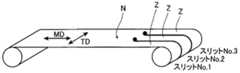
基板Zは、図7に示すように、基板Zよりも幅広の原反Nから、幅方向に、例えば、3つに切り出されて(スリットされて)形成されたものである。例えば、PETフィルムはTD方向(図7参照)、MD方向(図7参照)に延伸されるため、切り出された位置によって、熱収縮、ボーング(弓状)の程度が異なる。また、スリットされた高分子樹脂フィルムのロールであっても、ロールに巻き取る際の張力を巻取り長に応じて変化させること、または巻き取った後の内部応力などの影響により、ロールの巻き出し長に応じてTD方向(垂直方向(Transverse Direction))、MD方向(流れ方向(Machine Direction))の収縮、伸張の度合いが変化する。また、同じPETフィルムでもあっても、製造条件、製造者が異なれば、これらの性状も異なる。さらには、基板Zの構成をPETフィルムからPENフィルム等に変更すれば、当然収縮等の性状が異なる。Therefore, in the present invention, for the substrate Z, the
As shown in FIG. 7, the substrate Z is formed by cutting out (slit), for example, three pieces in the width direction from an original fabric N wider than the substrate Z. For example, since the PET film is stretched in the TD direction (see FIG. 7) and the MD direction (see FIG. 7), the degree of thermal shrinkage and boring (bow shape) varies depending on the cut out position. In addition, even when the roll of the polymer resin film is slit, it can be wound by changing the tension at the time of winding on the roll according to the winding length, or by the influence of internal stress after winding. The degree of contraction and expansion in the TD direction (Transverse Direction) and the MD direction (Machine Direction) varies depending on the length of the projection. Moreover, even if it is the same PET film, if the manufacturing conditions and the manufacturer are different, these properties are also different. Furthermore, if the configuration of the substrate Z is changed from a PET film to a PEN film or the like, the properties such as shrinkage naturally differ.
そこで、本実施形態においては、基板Zに関する基板情報が、入力部30を介して設定部37で取得される。この基板情報は、基板Zが製造される際の加工情報を含むものである。この加工情報は、具体的には、基板Zの原反Nから切り出された幅方向の位置の情報、例えば、図7におけるスリットナンバー、および基板Zが切り出された原反Nの長さ方向の位置の情報のことである。
記憶部35においては、基板Zの基板情報に基づいて、基板Zの伸縮強度が高い方向が記憶されている。基板Zの基板情報として、例えば、図7におけるスリットナンバー、および基板Zが切り出された原反Nの長さ方向の位置の情報と、基板Zの伸縮強度が高い方向とが関連付けて記憶されている。これにより、設定部37では、入力部30から入力された基板Zの基板情報について、記憶部35を参照して基板Zの伸縮強度が高い方向を特定することができる。Therefore, in the present embodiment, the board information regarding the board Z is acquired by the setting
In the
また、基板Zについて、収縮率、伸張率等の物性値を予め測定し、基板Zの伸縮強度が高い方向を予め特定しておく。この測定結果と基板情報とを対応付けて記憶部35に記憶しておく。さらには、基板Zについて、収縮率、伸張率等の物性値を予め測定し、基板Zの伸縮強度が高い方向と、基板Zの伸縮強度が高い方向の基板Zの長さ方向の分布を予め特定しておく。この結果と基板情報とを対応付けて記憶部35に記憶しておいてもよい。このように、記憶部35は、伸縮方向データベースとして機能する。
この場合においても、設定部37が、基板情報について、記憶部35を参照することにより、基板Zの伸縮強度が高い方向、および基板Zの伸縮強度が高い方向の基板Zの長さ方向の分布を特定することができる。Further, for the substrate Z, physical property values such as a shrinkage rate and an extension rate are measured in advance, and a direction in which the stretch strength of the substrate Z is high is specified in advance. The measurement result and the board information are stored in the
Also in this case, the setting
設定部37は、基板Zの伸縮強度が高い方向、および基板Zの伸縮強度が高い方向の基板Zの長さ方向の分布を特定した後、図6(c)に示すようにTFT60の配置方向αと基板Zの伸縮強度が高い方向(基板Zの伸びやすい方向EL)とが直交するように、TFT60の配置方向αの向き設定する。すなわち、トランジスタ形成領域Sの向きを設定する。その後、設定部37において、基板Zにおける出来上がりTFTのパターン寸法に応じたパターニング寸法の調整計算を行い、この計算結果に基づいてトランジスタ形成領域Sの最適配置を設定する。
設定部37から設定されたトランジスタ形成領域Sの向きの最適な設定情報が第1の画像処理部38および第2の画像処理部40、さらには、記憶部35に出力される。
制御部34は、記憶部35に記憶されたトランジスタ形成領域Sの向きの最適な設定情報に基づいて、マーク形成部41に、トランジスタ形成領域Sとなる領域の外縁部にアライメントマークMを形成させる。The setting
The optimum setting information of the orientation of the transistor formation region S set from the setting
The
なお、設定部37においては、基板Zの伸縮強度が高い方向、および基板Zの伸縮強度が高い方向の基板Zの長さ方向の分布に応じた、トランジスタ形成領域Sの配置パターンを予め設定しておき、特定された基板Zの伸縮強度が高い方向、およびその長さ方向の分布に基づいて、トランジスタ形成領域Sの配置を設定してもよい。
この場合、設定部37において、基板Zにおける出来上がりTFTのパターン寸法に応じたパターニング寸法の調整計算を行い、用いるトランジスタ形成領域Sの最適な配置パターンを設定する。その後、性状が大きく変らない範囲まではその設定した最適な配置パターンとし、次の性状の異なる(例えば、設定した閾値を越えた)領域、または基板Zが変わったときに、再度、配置パターンを設定する。In the
In this case, the setting
本実施形態においては、例えば、基板ZがMD方向の伸縮強度が高い場合、図8(a)に示すように、TFT60の配置方向αと基板Zの伸縮強度が高い方向(基板Zの伸びやすい方向EL)とが直交するように、トランジスタ形成領域Sを基板Zの幅方向WとTFT60の配置方向αを一致させるように設定する。この場合、マーク形成部41により、各トランジスタ形成領域Sの外縁部の4隅にアライメントマークMが形成される。
また、例えば、基板ZがTD方向の伸縮強度が高い場合、図8(b)に示すように、TFT60の配置方向αと基板Zの伸縮強度が高い方向(基板Zの伸びやすい方向EL)とが直交するように、トランジスタ形成領域Sを基板Zの搬送方向DとTFT60の配置方向αを一致させるように設定する。この場合、基板Zの幅方向wに、トランジスタ形成領域Sを2列に配置可能であれば、トランジスタ形成領域Sを2列配置する。なお、図8(b)の配置でも、マーク形成部41により、各トランジスタ形成領域Sの外縁部の4隅にアライメントマークMが形成される。In the present embodiment, for example, when the substrate Z has a high stretch strength in the MD direction, as shown in FIG. 8A, the direction in which the
Further, for example, when the substrate Z has a high stretching strength in the TD direction, as shown in FIG. 8B, the arrangement direction α of the
さらには、例えば、基板ZがMD方向の伸縮強度が高い領域Z1、Z3と、TD方向の伸縮強度が高い領域Z2とが混在する場合、図8(c)に示すように、TFT60の配置方向αと基板Zの伸縮強度が高い方向(基板Zの伸びやすい方向EL)とが直交するように、領域Z1〜領域Z3に応じて、トランジスタ形成領域Sの配置が設定される。この場合も、マーク形成部41により、向きが異なるトランジスタ形成領域Sの外縁部の4隅にアライメントマークMが形成される。
このように、向きが設定されたトランジスタ形成領域Sの向きの設定情報が第1の画像処理部38に出力されて、後述するように第1の画像処理部38において、設定情報に応じてTFTのパターンデータの向きが変更される。また、第2の画像処理部40においても、後述するようにインク滴56aの打滴位置を変更するために、設定情報に応じて打滴データが変更される。Further, for example, when the substrate Z includes regions Z1 and Z3 with high MD direction stretch strength and a region Z2 with high TD stretch strength, as shown in FIG. The arrangement of the transistor formation region S is set according to the regions Z1 to Z3 so that the arrangement direction α of the substrate Z and the direction in which the stretching strength of the substrate Z is high (the direction EL in which the substrate Z is easy to extend) are orthogonal to each other. . Also in this case, alignment marks M are formed by the
In this way, the setting information of the orientation of the transistor formation region S for which the orientation has been set is output to the first
なお、基板Zの基板情報は、入力部30を介して入力される以外にも、例えば、図2(a)に示すように、基板Zの端部に記録部Jを設け、この記録部Jに基板情報をバーコード等の形式で記録してもよい。この場合、例えば、歪みセンサ50で記録部Jを読み取り、読み取り結果が設定部37に出力されるようにする。
本実施形態においては、マーク形成部41を設けているため、トランジスタ形成領域Sの向きが変わっても、トランジスタ形成領域Sの外縁の4隅にアライメントマークMを形成することができる。In addition to inputting the substrate information of the substrate Z through the
In the present embodiment, since the
第1の画像処理部38は、描画データ作成部32、記憶部35、アライメント検出部36および設定部に接続されている。第1の画像処理部38には、描画データ作成部32からTFT60のパターンデータが入力され、アライメント検出部36で作成された基板Zの歪み情報、および設定部37からTFTの向き(トランジスタ形成領域Sの向き)の設定情報が入力される。
なお、TFT60のパターンデータは、ゲート電極62、半導体層64、およびソース電極66a・ドレイン電極66bの各位置、大きさの情報を含むものであり、例えば、描画データ作成部32により、ラスター形式の設計データ(ラスターデータ)に変換されたものである。The first
Note that the pattern data of the
第1の画像処理部38は、TFTの向き(トランジスタ形成領域Sの向き)の設定情報に基づいてトランジスタ形成領域Sの割り付けを行い、更に基板Zの歪み情報を許容範囲と比較し、基板Zの歪みが許容範囲を超える場合には、基板Zの歪み情報に応じて、トランジスタ形成領域Sにおけるレーザ光Bの照射位置を変更するために、露光データ(TFT60のパターンデータ)を補正する補正露光データを作成するものである。補正露光データは、設定されたTFTの向き(トランジスタ形成領域Sの向き)における基板Zの歪み応じたレーザ光Bの照射位置が補正されたものである。
第1の画像処理部38は、この補正露光データを駆動部52aに出力する。露光部52では、駆動部52aに入力された補正露光データに基づいて、レーザ光Bがパターン形成領域に照射される。
以下、基板Zの歪み情報を許容範囲と比較し、基板Zの歪みが許容範囲を超える場合のことを、基板Zに歪みがあるともいう。The first
The first
Hereinafter, when the distortion information of the substrate Z is compared with the allowable range, and the distortion of the substrate Z exceeds the allowable range, the substrate Z is also referred to as being distorted.
なお、第1の画像処理部38において、基板Zの歪み情報を許容範囲と比較し、基板Zの歪みが許容範囲内である場合には、TFTの向き(トランジスタ形成領域Sの向き)の設定情報に基づいてトランジスタ形成領域Sの割り付けを行うものの、基板Zの歪み応じたレーザ光Bの照射位置を補正せず、補正露光データを作成しない。このため、トランジスタ形成領域Sの向きについては設情報に基づいて変更されるものの、第1の画像処理部38に入力された露光データ(TFT60のパターンデータ)が補正されることなくそのまま露光部52の駆動部52aに出力される。露光部52では、駆動部52aに入力された露光データに基づいて、レーザ光Bがパターン形成領域に照射される。
以下、基板Zの歪み情報を許容範囲と比較し、基板Zの歪みが許容範囲内である場合のことを、基板Zに歪みがないともいう。In the first
Hereinafter, the distortion information of the substrate Z is compared with the allowable range, and the case where the distortion of the substrate Z is within the allowable range is also referred to as no distortion of the substrate Z.
第2の画像処理部40は、基板Zのトランジスタ形成領域Sに、TFT60の各構成部を形成するための組成を有する液体をインク滴56aとして打滴させるためのものである。この第2の画像処理部40は、入力部30、記憶部35、アライメント検出部36および設定部37に接続されている。第2の画像処理部40には、アライメント検出部36で作成された基板Zの歪み情報、および設定部37からTFTの向き(トランジスタ形成領域Sの向き)の設定情報が入力される。
なお、吐出部56においては、入力部30から入力されるTFTのパターンデータを変換することなく、打滴データとして利用することができる。The second
In the
第2の画像処理部40は、TFTの向き(トランジスタ形成領域Sの向き)の設定情報に基づいてトランジスタ形成領域Sの割り付けを行い、基板Zの歪み情報を許容範囲と比較し、基板Zの歪みが許容範囲を超える場合には、更に基板Zの歪み情報に応じて、トランジスタ形成領域Sにおけるインク滴56aの打滴位置を変更するために、打滴データを補正する補正打滴データを作成するものである。補正打滴データは、設定されたTFTの向き(トランジスタ形成領域Sの向き)における基板Zの歪み応じたインク滴56aの打滴位置が補正されたものである。
第2の画像処理部40は、この補正打滴データを吐出部56のドライバ(図示せず)に出力する。吐出部56では、ドライバに入力された補正打滴データに基づいて、インク滴56aがパターン形成領域、具体的には、TFTの各構成部の形成領域に打滴される。
なお、第2の画像処理部40において、基板Zの歪み情報を許容範囲と比較し、基板Zの歪みが許容範囲内である場合には、TFTの向き(トランジスタ形成領域Sの向き)の設定情報に基づいてトランジスタ形成領域Sの割り付けを行うものの、基板Zの歪み応じたインク滴56aの打滴位置を補正せず、補正打滴データを作成しない。このため、トランジスタ形成領域Sの向きについては設情報に基づいて変更されるものの、第2の画像処理部40に入力された打滴データが補正されることなくそのまま吐出部56のドライバに出力される。吐出部56では、ドライバに入力された打滴データに基づいて、インク滴56aがパターン形成領域、具体的には、TFTの各構成部の形成領域に打滴される。The second
The second
In the second
第1の画像処理部38および第2の画像処理部40においては、TFTの向き(トランジスタ形成領域Sの向き)の設定情報に基づいてトランジスタ形成領域Sの割り付けを行い、基板Zに歪みがある場合、例えば、基板Zの伸縮方向および伸縮量に対して、トランジスタ形成領域Sにおいて、その基板Zの伸縮を打ち消すように補正データが、それぞれオンデマンドで生成される。その後、このパターンの補正データに対応する補正露光データおよび補正打滴データがオンデマンドで生成される。ここでいう「補正露光データおよび補正打滴データ」とは、レーザ光照射用の露光データ及び打滴データに対して、シフト処理(面方向のずれ補正)、オフセット処理(厚み方向のずれ補正)、回転処理が施されたもの、拡大処理、縮小処理、台形補正処理(台形状に歪んだパターンを矩形状に補正する処理)が施されたものにTFTの向きの情報が含まれる。 In the first
本実施形態の製造装置10においては、改質処理ユニット14およびパターン形成ユニット16は共通のフィードバックループを有しており、アライメント検出部36から得られる同一の(共通の)基板Zの歪み情報、および設定部37で設定されたTFTの向き(トランジスタ形成領域Sの向き)の設定情報に基づいて、設定されたTFTの向き(トランジスタ形成領域Sの向き)におけるレーザ光Bの照射補正およびインク滴の打滴補正を行うように構成されている。このため、レーザ光Bの照射補正およびインク滴の打滴補正の精度を高くすることができ、しかも、共通の基板の歪み情報を用いているため、補正データの作成を速くすることができ、補正に要するコストも低くすることができる。
なお、第1の画像処理部38および第2の画像処理部40の機能を1つにまとめて、単に画像処理部としてもよい。In the
The functions of the first
また、本実施形態においては、基板Zの表面等に絶縁層形成するための絶縁体を塗布する塗布部を設けてもよい。
さらに、インク滴56aを硬化させるために、必要に応じて、紫外線を照射する紫外線照射手段(図示せず)、または所定の温度で加熱処理を行うための加熱手段(図示せず)等を設けてもよい。In the present embodiment, an application portion for applying an insulator for forming an insulating layer on the surface of the substrate Z may be provided.
Furthermore, in order to cure the
本実施形態においては、設定されたトランジスタ形成領域Sに以下に示すように、TFT60を形成することができる。
以下、本実施形態のTFT60の製造方法について、図9および図10(a)〜(i)に基づいて説明する。In the present embodiment, the
Hereinafter, a manufacturing method of the
本実施形態においては、TFT60を形成する先立ち、上述のように、用いる基板Zについての基板情報を設定部37に取得させる(ステップS10)。
次に、設定部37が、この基板情報について、記憶部35を参照し、基板Zの伸縮強度が高い方向が特定される(ステップS12)。
次に、基板Zの伸縮強度が高い方向に基づいて、トランジスタ形成領域Sの最適配置を設定する(ステップS14)。このように、設定されたトランジスタ形成領域Sの向きの設定情報が、記憶部35、第1の画像処理部38に出力される。トランジスタ形成領域Sの向きの設定情報に応じて、マーク形成部41によりトランジスタ形成領域Sの外縁部にアライメントマークMが形成される。これにより、TFTの製造の用意ができた。In the present embodiment, before forming the
Next, the setting
Next, the optimal arrangement of the transistor formation region S is set based on the direction in which the expansion / contraction strength of the substrate Z is high (step S14). Thus, the setting information of the orientation of the set transistor formation region S is output to the
第1の画像処理部38においては、TFTの向き(トランジスタ形成領域Sの向き)の設定情報に基づいてトランジスタ形成領域Sの割り付けを行い、基板Zに歪みがある場合、トランジスタ形成領域Sにおいて、基板Zの歪みを打ち消すように補正データが作成される。なお、第2の画像処理部40においても、TFTの向き(トランジスタ形成領域Sの向き)の設定情報に基づいてトランジスタ形成領域Sの割り付けを行い、露光部52により露光された領域にインク滴56a打滴するように打滴位置が変更される。これにより、露光部52により、TFTを構成するゲート電極62、半導体層64、およびソース電極66a・ドレイン電極66bの各形成領域を、露光部52により、親液性にするための露光を行うことができる(ステップS16)。 In the first
以下、TFTの製造工程について、より具体的に説明する。
本実施形態においては、TFT60のゲート電極62、半導体層64、およびソース電極66a・ドレイン電極66bを形成するために、吐出部56からインク滴56aとして吐出させる組成のものに対して、露光部52の露光により親液性となる、ゲート電極62、半導体層64、およびソース電極66a・ドレイン電極66bを電気的に絶縁する絶縁体が予め選択されている。Hereinafter, the manufacturing process of the TFT will be described more specifically.
In the present embodiment, in order to form the
本実施形態において、図10(a)に示すように、基板Zの表面に、電気絶縁性を備えるとともに、露光部52の露光により親液性になる第1の絶縁層80を形成する。
この第1の絶縁層80は、基板Zの表面に、例えば、製造装置10とは別の塗布装置により、塗布により形成されたものである。なお、製造装置10に塗布部がある場合には、第1の絶縁層80は塗布部により形成される。In the present embodiment, as shown in FIG. 10A, a first insulating
The first insulating
次に、図10(a)に示す第1の絶縁層80が形成された基板Zをロール状にし、基板ロールとした後、供給室12の巻取り軸42に取り付ける。その後、基板Zを巻き回し、ガイドローラ44を経て、マーク形成室13、計測室14、改質室16、パターン形成室18を、それぞれガイドローラ49を経て、巻取り室20に搬送される。巻取り室20においては、ガイドローラ48を経て、巻取り軸46に基板Zが巻き取られる。このように、基板Zを、所定の搬送経路に通す。 Next, the substrate Z on which the first insulating
次に、マーク形成室13において、マーク形成部41により、設定されたトランジスタ形成領域Sの配置情報に応じて、トランジスタ形成領域Sの外縁部にアライメントマークMがり形成される。
そして、計測室14において、歪みセンサ50により、基板Zに形成された上述のトランジスタ形成領域Sの4つのアライメントマークMを撮像し、4つのアライメントマークMの画像データを得る。アライメント検出部36で基板の歪み情報が作成されて、記憶部35、第1の画像処理部38、第2の画像処理部40に出力される。
一方、基板Zが搬送され、トランジスタ形成領域Sが改質室16に搬送される。
このとき、基板Zに歪みがない場合には、TFTの向き(トランジスタ形成領域Sの向き)の設定情報に基づいてトランジスタ形成領域Sの割り付けを行うものの、基板Zの歪み応じたレーザ光Bの照射位置を補正せず、TFT60のパターンデータに基づいて、図10(b)に示すように、ゲート電極62の形成領域E1に反応ガスを供給しつつ、露光部52により形成領域E1を露光して改質処理をする。すなわち、ゲート電極62を形成するための組成を有するインク滴56aに対して親液性にする。Next, in the
In the
On the other hand, the substrate Z is transferred, and the transistor formation region S is transferred to the reforming
At this time, if the substrate Z is not distorted, the transistor formation region S is allocated based on the setting information of the TFT direction (transistor formation region S), but the laser beam B corresponding to the distortion of the substrate Z is allocated. without correcting the irradiation position, based on the pattern data of the
次に、基板Zを搬送し、ゲート電極62の形成領域E1が改質処理されたトランジスタ形成領域Sをパターン形成室18に搬送する。
次に、ゲート電極62の形成領域E1に、打滴データに基づいて、吐出部56から、ゲート電極62となるインクのインク滴56aが打滴される。このとき、基板Zに歪みがないため、TFTの向き(トランジスタ形成領域Sの向き)の設定情報に基づいてトランジスタ形成領域Sの割り付けを行うものの、基板Zの歪み応じたインク滴56aの打滴位置を補正はしない。すなわち、打滴データの補正はされない。このようにして、図10(c)に示すように、ゲート電極62が形成される。
なお、インク滴56aを硬化させるために、必要に応じて、紫外線照射手段(図示せず)により紫外線を照射するか、または加熱手段(図示せず)により所定の温度で加熱処理を行う。Next, the substrate is conveyed Z, forming regions E1 of the
Then, the formation area E1 of the
In order to cure the
一方、基板Zに歪みがある場合、記憶部35においては、TFT60の製造工程のどの時点での基板Zの歪みであるかが、基板Zの歪み情報として記憶される。
第1の画像処理部38において、TFTの向き(トランジスタ形成領域Sの向き)の設定情報に基づいてトランジスタ形成領域Sの割り付けを行い、トランジスタ形成領域Sにおけるレーザ光Bの照射位置を変更するために、基板Zの歪み情報(基板Zの伸縮の方向および基板Zの伸縮量)に基づいて、ゲート電極62の形成位置、形状などの補正値(スケーリング値kx、ky)を算出し、このスケーリング値に基づいてTFTのパターンデータのうち、ゲート電極62に関するデータを補正する補正露光ゲート電極データを作成する。この補正露光ゲート電極データに基づいて、図10(b)に示すように、ゲート電極62の形成領域E1に反応ガスを供給しつつ、露光部52により形成領域E1を露光して改質処理をする。すなわち、ゲート電極62を形成するための組成を有するインク滴56aに対して親液性にする。On the other hand, when the substrate Z is distorted, the
In the first
次に、基板Zを搬送し、ゲート電極62の形成領域E1が改質処理されたトランジスタ形成領域Sをパターン形成室18に搬送する。
次に、第2の画像処理部40において、改質処理されたゲート電極62となる形成領域E1にインクを打滴するために、第1の画像処理部38と同じくTFTの向き(トランジスタ形成領域Sの向き)の設定情報に基づいてトランジスタ形成領域Sの割り付けを行い、基板Zの歪み情報(基板Zの伸縮の方向および基板Zの伸縮量)に基づいて、ゲート電極62の形成位置、形状などの補正値(スケーリング値kx、ky)を算出し、このスケーリング値に基づいてTFTのパターンデータのうち、ゲート電極62に関するデータを補正する補正打滴ゲート電極データを作成する。この補正打滴ゲート電極データにより、改質処理されたゲート電極62となる形成領域E1にインク滴56aを打滴することができる。これにより、図10(c)に示すように、ゲート電極62が形成される。
なお、インク滴56aを硬化させるために、必要に応じて、紫外線照射手段(図示せず)により紫外線を照射するか、または加熱手段(図示せず)により所定の温度で加熱処理を行う。
次に、ゲート電極62が形成された基板Zが、巻取り軸46に巻き取られる。これにより、ゲート電極62の形成工程が終了する。Next, the substrate is conveyed Z, forming regions E1 of the
Then, in the second
In order to cure the
Next, the substrate Z on which the
次に、ゲート電極62が形成され巻取り軸46に巻き取られた基板Zを巻取り室20から外し、例えば、別のロール・ツー・ロールタイプの塗布装置に基板Zをセットする。そして、図10(d)に示すように、ゲート電極62および第1の絶縁層80を覆うようにして第2の絶縁層82を形成する。この第2の絶縁層82は、ゲート絶縁膜として機能するものである。なお、第2の絶縁層82も、電気絶縁性を備えるとともに、露光部52の露光により親液性になるものである。 Next, the substrate Z on which the
次に、再度、上述のように製造装置10の供給室12の巻取り軸42に取り付け、基板Zを、所定の搬送経路に通す。
次に、再度、計測室14において、基板Zに形成された上述のトランジスタ形成領域Sの4つのアライメントマークMを撮像し、4つのアライメントマークMの画像データを得、アライメント検出部36で基板の歪み情報が作成されて、記憶部35、第1の画像処理部38、第2の画像処理部40に出力される。一方、基板Zが搬送されて、トランジスタ形成領域Sが改質室16に搬送される。
このとき、基板Zに歪みがない場合には、TFTの向き(トランジスタ形成領域Sの向き)の設定情報に基づいてトランジスタ形成領域Sの割り付けを行うものの、基板Zの歪み応じたレーザ光Bの照射位置を補正せず、TFT60のパターンデータに基づいて、図10(e)に示すように、半導体層64の形成領域E2に反応ガスを供給しつつ、露光部52により形成領域E2を露光して改質処理をする。すなわち、半導体層64を形成するための組成を有するインク滴56aに対して親液性にする。Next, the substrate Z is again attached to the take-up
Next, in the
At this time, if the substrate Z is not distorted, the transistor formation region S is allocated based on the setting information of the TFT direction (transistor formation region S), but the laser beam B corresponding to the distortion of the substrate Z is allocated. without correcting the irradiation position, based on the pattern data of the
次に、基板Zを搬送し、半導体層64の形成領域E2が改質処理されたトランジスタ形成領域Sをパターン形成室18に搬送する。
次に、半導体層64の形成領域E2に、打滴データに基づいて、吐出部56から、半導体層64となるインクのインク滴56aが打滴される。このとき、基板Zに歪みがないため、TFTの向き(トランジスタ形成領域Sの向き)の設定情報に基づいてトランジスタ形成領域Sの割り付けを行うものの、基板Zの歪み応じたインク滴56aの打滴位置を補正はしない。すなわち、打滴データの補正はされない。このようにして、図10(f)に示すように、半導体層64が形成される。Next, the substrate is conveyed Z, forming area E2 of the
Next,
なお、インク滴56aを硬化させるために、必要に応じて、紫外線照射手段(図示せず)により紫外線を照射するか、または加熱手段(図示せず)により所定の温度で加熱処理を行う。 In order to cure the
一方、基板Zに歪みがある場合、記憶部35においては、TFT60の製造工程のどの時点での基板Zの歪みであるかが、基板Zの歪み情報として記憶される。
第1の画像処理部38において、TFTの向き(トランジスタ形成領域Sの向き)の設定情報に基づいてトランジスタ形成領域Sの割り付けを行い、トランジスタ形成領域Sにおけるレーザ光Bの照射位置を変更するために、基板Zの歪み情報(基板Zの伸縮の方向および基板Zの伸縮量)に基づいて、半導体層64の形成位置、形状などの補正値(スケーリング値kx、ky)を算出し、このスケーリング値に基づいてTFTのパターンデータのうち、半導体層64に関するデータを補正する補正露光半導体層データを作成する。この補正露光半導体層データに基づいて、図10(e)に示すように、半導体層64の形成領域E2に反応ガスを供給しつつ、露光部52により形成領域E2を露光して改質処理をする。すなわち、半導体層64を形成するための組成を有するインク滴56aに対して親液性にする。On the other hand, when the substrate Z is distorted, the
In the first
次に、基板Zを搬送し、半導体層64の形成領域E2が改質処理されたトランジスタ形成領域Sをパターン形成室18に搬送する。
次に、第2の画像処理部40において、第1の画像処理部38と同じくTFTの向き(トランジスタ形成領域Sの向き)の設定情報に基づいてトランジスタ形成領域Sの割り付けを行い、基板Zの歪み情報(基板Zの伸縮の方向および基板Zの伸縮量)に基づいて、改質処理された半導体層64となる形成領域E1にインクを打滴するために、半導体層64の形成位置、形状などの補正値(スケーリング値kx、ky)を算出し、このスケーリング値に基づいてTFTのパターンデータのうち、半導体層64に関するデータを補正する補正打滴半導体層データを作成する。この補正打滴半導体層データにより、改質処理された半導体層64となる形成領域E2にインク滴56aを打滴することができる。
この場合においても、インク滴56aを硬化させるために、必要に応じて、紫外線照射手段(図示せず)により紫外線を照射するか、または加熱手段(図示せず)により所定の温度で加熱処理を行う。
次に、半導体層64が形成された基板Zが、巻取り軸46に巻き取られる。これにより、半導体層64の形成工程が終了する。Next, the substrate is conveyed Z, forming area E2 of the
Next, in the second
Also in this case, in order to cure the
Next, the substrate Z on which the
次に、ソース電極66aおよびドレイン電極66bを形成するために、半導体層64が形成され巻取り軸46に巻き取られた基板Zを巻取り室20から外し、上述のように、製造装置10の供給室12の巻取り軸42に取り付け、基板Zを、所定の搬送経路に通す。
次に、再度、計測室14において、基板Zに形成された上述のトランジスタ形成領域Sの4つのアライメントマークMを撮像し、4つのアライメントマークMの画像データを得、アライメント検出部36で基板の歪み情報が作成されて、記憶部35、第1の画像処理部38、第2の画像処理部40に出力される。一方、基板Zが搬送されて、トランジスタ形成領域Sが改質室16に搬送される。
このとき、基板Zに歪みがない場合には、TFTの向き(トランジスタ形成領域Sの向き)の設定情報に基づいてトランジスタ形成領域Sの割り付けを行うものの、基板Zの歪み応じたレーザ光Bの照射位置を補正せず、TFTのパターンデータに基づいて、図10(g)に示すように、ソース電極66aの形成領域E3およびドレイン電極66bの形成領域E4に反応ガスを供給しつつ、露光部52により形成領域E3および形成領域E4を露光して改質処理をする。すなわち、ソース電極66aおよびドレイン電極66bを形成するための組成を有するインク滴56aに対して親液性にする。Next, in order to form the
Next, in the
At this time, if the substrate Z is not distorted, the transistor formation region S is allocated based on the setting information of the TFT direction (transistor formation region S), but the laser beam B corresponding to the distortion of the substrate Z is allocated. without correcting the irradiation position, based on the pattern data of the TFT, as shown in FIG. 10 (g), while supplying a reaction gas to the forming area E4 forming region E3 and the
次に、基板Zを搬送し、ソース電極66aの形成領域E3およびドレイン電極66bの形成領域E4が改質処理されたトランジスタ形成領域Sをパターン形成室18に搬送する。
次に、ソース電極66aの形成領域E3およびドレイン電極66bの形成領域E4に、打滴データに基づいて、吐出部56から、ソース電極66aおよびドレイン電極66bとなるインクのインク滴56aが打滴される。このとき、基板Zに歪みがないため、TFTの向き(トランジスタ形成領域Sの向き)の設定情報に基づいてトランジスタ形成領域Sの割り付けを行うものの、基板Zの歪み応じたインク滴56aの打滴位置を補正はしない。すなわち、打滴データの補正はされない。このようにして、図10(h)に示すように、ソース電極66aおよびドレイン電極66bが形成される。Next, the substrate is conveyed Z, conveys the transistor forming region S formed region E4 was processed reforming forming region E3 and the
Next, the forming regionE 4 forming regionE 3 and the
なお、インク滴56aを硬化させるために、必要に応じて、紫外線照射手段(図示せず)により紫外線を照射するか、または加熱手段(図示せず)により所定の温度で加熱処理を行う。 In order to cure the
一方、基板Zに歪みがある場合、記憶部35においては、TFT60の製造工程のどの時点での基板Zの歪みであるかが、基板Zの歪み情報として記憶される。
第1の画像処理部38において、TFTの向き(トランジスタ形成領域Sの向き)の設定情報に基づいてトランジスタ形成領域Sの割り付けを行い、トランジスタ形成領域Sにおけるレーザ光Bの照射位置を変更するために、基板Zの歪み情報(基板Zの伸縮の方向および基板Zの伸縮量)に基づいて、ソース電極66aおよびドレイン電極66bの形成位置、形状などの補正値(スケーリング値kx、ky)を算出し、このスケーリング値に基づいてTFTのパターンデータのうち、ソース電極66aおよびドレイン電極66bに関するデータを補正する補正露光ソース電極およびドレイン電極データを作成する。この補正露光ソース電極およびドレイン電極データに基づいて、図10(h)に示すように、ソース電極66aの形成領域E3およびドレイン電極66bの形成領域E4に反応ガスを供給しつつ、露光部52により形成領域E2を露光して改質処理をする。すなわち、ソース電極66aおよびドレイン電極66bを形成するための組成を有するインク滴56aに対して親液性にする。On the other hand, when the substrate Z is distorted, the
In the first
次に、基板Zを搬送し、ソース電極66aの形成領域E3およびドレイン電極66bの形成領域E4が改質処理されたトランジスタ形成領域Sをパターン形成室18に搬送する。
次に、第2の画像処理部40において、ソース電極66aの形成領域E3およびドレイン電極66bの形成領域E4にインクを打滴するために、第1の画像処理部38と同じくTFTの向き(トランジスタ形成領域Sの向き)の設定情報に基づいてトランジスタ形成領域Sの割り付けを行い、基板Zの歪み情報(基板Zの伸縮の方向および基板Zの伸縮量)に基づいて、ソース電極66aおよびドレイン電極66bの形成位置、形状などの補正値(スケーリング値kx、ky)を算出し、このスケーリング値に基づいてTFTのパターンデータのうち、ソース電極66aおよびドレイン電極66bに関するデータを補正する補正打滴ソース電極およびドレイン電極データを作成する。この補正打滴ソース電極およびドレイン電極データにより、改質処理されたソース電極66aの形成領域E3およびドレイン電極66bの形成領域E4にインク滴56aを打滴することができる。
この場合においても、インク滴56aを硬化させるために、必要に応じて、紫外線照射手段(図示せず)により紫外線を照射するか、または加熱手段(図示せず)により所定の温度で加熱処理を行う。
次に、ソース電極66aおよびドレイン電極66bが形成された基板Zが、巻取り軸46に巻き取られる。これにより、ソース電極66aおよびドレイン電極66bの形成工程が終了する。Next, the substrate is conveyed Z, conveys the transistor forming region S formed region E4 was processed reforming forming region E3 and the
Then, in the second
Also in this case, in order to cure the
Next, the substrate Z on which the
次に、ソース電極66aおよびドレイン電極66bが形成され巻取り軸46に巻き取られた基板Zを巻取り室20から外し、例えば、別のロール・ツー・ロールタイプの塗布装置に基板Zをセットする。そして、図10(i)に示すように、ソース電極66aおよびドレイン電極66bならびに半導体層64を覆うようにして第3の絶縁層84を形成する。この第2の絶縁層84は、保護膜として機能するものである。このようにして、TFT60が形成される。なお、この図10(i)に示すTFT60の模式的断面図は、図6(a)のH−H線断面に相当するものである。 Next, the substrate Z formed with the
本実施形態においては、基板Zの伸縮強度が高い方向に応じて、TFT60の配置方向αの向きを、チャネル長Lが変動しないように、すなわち、TFT特性が変動しないように設定してTFT60が形成される。このため、フレキシブルな基板を用い、この基板に異方性があっても、高い精度でTFT60を形成することができる。これにより、TFT60をディスプレイに適用した場合、各画素のドレイン電流値のバラツキを軽減することができ、結果として輝度バラツキを軽減することができる。 In the present embodiment, the direction of the arrangement direction α of the
また、本実施形態においては、TFT60のゲート電極62、半導体層64およびソース電極66a、ドレイン電極66bの形成位置の補正にラスターデータを用いたが、本発明はこれに限定されるものではなく、ベクターデータを用いることもできる。 In the present embodiment, raster data is used to correct the formation positions of the
なお、本発明においては、上述のTFT60の製造方法を、コンピュータを用いて実行させるプログラム、およびそのプログラムが記録された記録媒体の形態とすることもできる。この場合、例えば、入力部30を介してTFT60を製造するためのプログラムが記憶部35に、一旦記憶され、その後、実行されて制御部34により、製造装置10の各構成が制御されて、TFT60を製造することもできる。 In the present invention, the above-described manufacturing method of the
以下、TFT60の各構成、ゲート電極62、半導体層64、およびソース電極66a・ドレイン電極66b、および各絶縁層の製造に用いられる材料について具体的に説明する。
本実施形態の製造装置10は、ロール・ツー・ロール方式であるため、基板Zとしては、生産性、フレキシビリティなどの観点から、樹脂フィルムが用いられる。この樹脂フィルムには特に制限がなく、その材料、形状、構造、厚み等については公知のものの中から適宜選択することができる。
樹脂フィルムとしては、例えば、ポリエチレンテレフタレート(PET)、ポリエチレンナフタレート(PEN)変性ポリエステル等のポリエステル系樹脂フィルム、ポリエチレン(PE)樹脂フィルム、ポリプロピレン(PP)樹脂フィルム、ポリスチレン樹脂フィルム、環状オレフィン系樹脂等のポリオレフィン類樹脂フィルム、ポリ塩化ビニル、ポリ塩化ビニリデン等のビニル系樹脂フィルム、ポリエーテルエーテルケトン(PEEK)樹脂フィルム、ポリサルホン(PSF)樹脂フィルム、ポリエーテルサルホン(PES)樹脂フィルム、ポリカーボネート(PC)樹脂フィルム、ポリアミド樹脂フィルム、ポリイミド樹脂フィルム、アクリル樹脂フィルム、トリアセチルセルロース(TAC)樹脂フィルム等を挙げることができる。Hereinafter, each structure of TFT60, the
Since the
Examples of the resin film include polyester resin films such as polyethylene terephthalate (PET) and polyethylene naphthalate (PEN) modified polyester, polyethylene (PE) resin film, polypropylene (PP) resin film, polystyrene resin film, and cyclic olefin resin. Polyolefin resin films such as polyvinyl chloride, polyvinyl resin such as polyvinyl chloride, polyvinylidene chloride, polyether ether ketone (PEEK) resin film, polysulfone (PSF) resin film, polyether sulfone (PES) resin film, polycarbonate ( PC) resin film, polyamide resin film, polyimide resin film, acrylic resin film, triacetyl cellulose (TAC) resin film, etc.
TFTをディスプレイ等の用途に用いる場合には、基板Zとしては、透明樹脂フィルムが好ましく、可視域の波長における光線透過率が80%以上である樹脂フィルムであればよい。中でも透明性、耐熱性、取り扱いやすさ、強度及びコストの点から、二軸延伸ポリエチレンテレフタレートフィルム、二軸延伸ポリエチレンナフタレートフィルム、ポリエーテルサルホンフィルム、ポリカーボネートフィルムであることが好ましく、二軸延伸ポリエチレンテレフタレートフィルム、二軸延伸ポリエチレンナフタレートフィルムであることがより好ましい。 When the TFT is used for a display or the like, the substrate Z is preferably a transparent resin film and may be a resin film having a light transmittance of 80% or more at a visible wavelength. Among these, from the viewpoint of transparency, heat resistance, ease of handling, strength and cost, it is preferably a biaxially stretched polyethylene terephthalate film, a biaxially stretched polyethylene naphthalate film, a polyethersulfone film, or a polycarbonate film, and biaxially stretched. More preferred are polyethylene terephthalate films and biaxially stretched polyethylene naphthalate films.
一方、枚葉式の場合には、基板Zとして、Siウエハ、石英ガラス、ガラス、プラスチック、金属板など各種のものを用いることができ、基材の表面に半導体膜、金属膜、誘電体膜、有機膜などが積層成形できるのであればよい。 On the other hand, in the case of a single wafer type, various substrates such as a Si wafer, quartz glass, glass, plastic, and metal plate can be used as the substrate Z, and a semiconductor film, a metal film, and a dielectric film are formed on the surface of the substrate. Any organic film can be used as long as it can be laminated.
ゲート電極62、半導体層64、およびソース電極66a・ドレイン電極66bを電気的に絶縁する絶縁体(絶縁層)は、後述する親液性・撥液性材料により構成されるものであり、その厚さ(層厚)は、0.001μm〜1μmであることが好ましく、特に好ましくは0.01〜0.1μmである。
上述のゲート電極62、半導体層64、およびソース電極66a・ドレイン電極66bを電気的に絶縁する絶縁体(絶縁層)を構成する親液性・撥液性材料においては、エネルギー照射していない部分、すなわち、撥液性領域においては、塗布液との接触角が、50°以上、中でも90°以上であることが好ましい。
また、上述の親液性・撥液性材料においては、エネルギー照射された部分、すなわち、親液性領域においては、塗布液との接触角が、40°以下、中でも20°以下、特に好ましくは、10°以下である。
なお、撥液性領域と親液性領域の濡れ性の差は、表面張力で10mN/m以上であることが好ましい。The insulator (insulating layer) that electrically insulates the
In the lyophilic / liquid repellent material constituting the insulator (insulating layer) that electrically insulates the
Further, in the lyophilic and lyophobic material described above, the contact angle with the coating solution is 40 ° or less, particularly 20 ° or less, particularly preferably in the portion irradiated with energy, that is, in the lyophilic region. 10 degrees or less.
The difference in wettability between the liquid repellent region and the lyophilic region is preferably 10 mN / m or more in terms of surface tension.
親液性・撥液性材料において、無機材料としては、酸化チタン(TiO2)、酸化亜鉛(ZnO)、酸化スズ(SnO2)、チタン酸ストロンチウム(SrTiO3)、酸化タングステン(WO3)、酸化ビスマス(Bi2O3)、および酸化鉄(Fe2O3)など酸化物を上げることが出来る。これら酸化物を1種または2種以上選択して用いることができ、例えば、二酸化チタンであれば、アナターゼ型とルチル型がありいずれも使用することができるが、アナターゼ型の二酸化チタンが好ましい。In the lyophilic / liquid repellent material, inorganic materials include titanium oxide (TiO2 ), zinc oxide (ZnO), tin oxide (SnO2 ), strontium titanate (SrTiO3 ), tungsten oxide (WO3 ), Oxides such as bismuth oxide (Bi2 O3 ) and iron oxide (Fe2 O3 ) can be raised. One or more of these oxides can be selected and used. For example, if titanium dioxide is used, there are anatase type and rutile type, and both can be used, but anatase type titanium dioxide is preferable.
親液性・撥液性材料において、バインダーとしては、主骨格が酸化物の光励起により分解されないような高い結合エネルギーを有するものを使用することがよく、酸化物の作用により濡れ性を変化させる機能をバインダーに持たせる場合には、バインダーの主骨格が前記の酸化物の光励起により分解されないような高い結合エネルギーを有するものであって、酸化物の作用により分解されるような有機置換基を有するものが好ましく、例えば、ゾルゲル反応等によりクロロまたはアルコキシシラン等を加水分解、重縮合して大きな強度を発揮するオルガノポリシロキサン、撥水牲や撥油性に優れた反応性シリコーンを架橋したオルガノポリシロキサン等を挙げることができる。
また、前記のオルガノポリシロキサンとともに、ジメチルポリシロキサンのような架橋反応をしない安定なオルガノシリコン化合物をバインダーに混合してもよい。
また、エネルギー照射に酸化物の作用により分解され、これにより酸化物含有層上の濡れ性を変化させることができる分解物質を酸化物含有層中に含有させることもできる。このような分解物質としては、酸化物の作用により分解し、かつ分解されることにより光触媒含有層表面の濡れ性を変化させる機能を有する界面活性剤を挙げることができる。In lyophilic and liquid repellent materials, it is preferable to use a binder with a high binding energy such that the main skeleton is not decomposed by photoexcitation of the oxide, and the function of changing the wettability by the action of the oxide When the binder is provided with a binder, the main skeleton of the binder has a high binding energy that does not decompose by photoexcitation of the oxide, and has an organic substituent that can be decomposed by the action of the oxide. Preferred are, for example, organopolysiloxanes that exhibit high strength by hydrolyzing and polycondensing chloro or alkoxysilane, etc. by sol-gel reaction, etc., organopolysiloxanes crosslinked with reactive silicones that are excellent in water and oil repellency Etc.
In addition to the organopolysiloxane, a stable organosilicon compound that does not undergo a crosslinking reaction, such as dimethylpolysiloxane, may be mixed in the binder.
In addition, a decomposition substance that can be decomposed by the action of an oxide upon energy irradiation and thereby change the wettability on the oxide-containing layer can be contained in the oxide-containing layer. As such a decomposition substance, a surfactant having a function of decomposing by the action of an oxide and changing the wettability of the surface of the photocatalyst containing layer by being decomposed can be exemplified.
具体的には、フッ素系あるいはシリコーン系の非イオン界面活性剤を挙げることができ、また、カチオン系界面活性剤、アニオン系界面活性剤、両性界面活性剤を用いることもできる。界面活性剤の他にも、ポリビニルアルコール、不飽和ポリエステル、アクリル樹脂、ポリエチレン、ジアリルフタレート、エチレンプロピレンジエンモノマー、エポキシ樹脂、フェノール樹脂、ポリウレタン、メラミン樹脂、ポリカーボネート、ポリ塩化ビニル、ポリアミド、ポリイミド、スチレンブタジエンゴム、クロロプレンゴム、ポリプロピレン、ポリブチレン、ポリスチレン、ポリ酢酸ビニル、ナイロン、ポリエステル、ポリブタジエン、ポリベンズイミダゾール、ポリアクリルニトリル、エピクロルヒドリン、ポリサルファイド、ポリイソプレン等のオリゴマー、ポリマー等を挙げることができる。
そのほか、親液性化する化合物としては、ジアゾニウム塩、スルホニウム塩、ヨードオニウム塩等のオニウム塩、O−ニトロベンジルスルホネ―ト化合物、増感剤と併用したP−ニトロベンジルスルホンネ―ト化合物、1,2,3−トリスベンゼン、N―イミドスルホネ―ト化合物、オキシムスルホネ―ト化合物、α―ケトスルホネ―ト化合物、ナフトキノンジアジド−4−スルホネ―ト化合物、ジアゾジスルホン化合物、ジスルホン化合物、ケトスルホン化合物、O−ニトロベンジルエステル化合物、m―アルコキシベンジルエステル化合物、O−ニトロベンジルアミド化合物、ベンゾイソエステル化合物、フェナシルエステル化合物、2,4−ジニトロベンゼンスルフォニルエステル、2−ジアゾー1,3ジケトン化合物、フェノールエステル化合物、O−ニトロベンジルフェノール化合物、2,5−シクロヘキサジエノン化合物、スルホン化ポリオレフィン、アリールジアゾスルホネート塩などがある。Specific examples include fluorine-based or silicone-based nonionic surfactants, and cationic surfactants, anionic surfactants, and amphoteric surfactants can also be used. In addition to surfactants, polyvinyl alcohol, unsaturated polyester, acrylic resin, polyethylene, diallyl phthalate, ethylene propylene diene monomer, epoxy resin, phenol resin, polyurethane, melamine resin, polycarbonate, polyvinyl chloride, polyamide, polyimide, styrene Examples include butadiene rubber, chloroprene rubber, polypropylene, polybutylene, polystyrene, polyvinyl acetate, nylon, polyester, polybutadiene, polybenzimidazole, polyacrylonitrile, epichlorohydrin, polysulfide, polyisoprene, and other oligomers and polymers.
In addition, lyophilic compounds include onium salts such as diazonium salts, sulfonium salts, iodoonium salts, O-nitrobenzyl sulfonate compounds, and P-nitrobenzyl sulfonate compounds used in combination with sensitizers. 1,2,3-trisbenzene, N-imide sulfonate compound, oxime sulfonate compound, α-keto sulfonate compound, naphthoquinone diazide-4-sulfonate compound, diazodisulfone compound, disulfone compound, ketosulfone compound O-nitrobenzyl ester compound, m-alkoxybenzyl ester compound, O-nitrobenzylamide compound, benzoisoester compound, phenacyl ester compound, 2,4-dinitrobenzenesulfonyl ester, 2-
本実施形態においては、親液性・撥液性材料として機能し、エネルギーの付与によって臨界表面張力が大きく変化する材料(親疎水変換材料)としては、側鎖に疎水性基を含む高分子材料も挙げられる。
ポリイミドや(メタ)アクリレート等の骨格を有する主鎖に直接あるいは結合基を介して疎水性基を有する側鎖が結合しているものを挙げることができる。疎水性基としては、末端構造が−CF2CH3、−CF2CF3、−CF(CF3)2、−C(CF3)3、−CF2H、−CFH2等である基が挙げられる。分子鎖同士を配向し易くするためには炭素鎖長の長い基が好ましく、炭素数4以上のものがより好ましい。さらには、アルキル基の水素原子の2個以上がフッ素原子に置換されたポリフルオロアルキル基が好ましく、特に炭素数4〜20のRf基が好ましく、とりわけ、炭素数6〜12のポリフルオロアルキル基が好ましい。ポリフルオロアルキル基には直鎖構造あるいは分岐構造があるが、直鎖構造の方が好ましい。さらに、疎水性基は、アルキル基の水素原子の実質的に全てがフッ素原子に置換されたパーフルオロアルキル基が好ましい。パーフルオロアルキル基はCnF2n+1−(ただし、nは4〜16の整数)で表わされる基が好ましく、特に、nが6〜12の整数である場合の該基が好ましい。パーフルオロアルキル基は直鎖構造であっても分岐構造であってもよく、直鎖構造が好ましい。さらに、疎水性基としては、フッ素原子を含まない−CH2CH3、−CH(CH3)2、−C(CH3)3等の末端構造を有する基を挙げることができる。この場合にも、分子鎖同士を配向し易くするためには炭素鎖長の長い基が好ましく、炭素数4以上のものがより好ましい。疎水性基は直鎖構造であっても分岐構造であってもよいが、直鎖構造の方が好ましい。上記アルキル基はハロゲン原子、シアノ基、フェニル基、ヒドロキシル基、カルボキシル基又は炭素数1〜12の直鎖、分岐鎖もしくは環状のアルキル基やアルコキシ基で置換されたフェニル基を含有していてもよい。側鎖に疎水性基を有する高分子材料としては、ポリイミドを含む高分子材料が挙げられる。
本実施形態に用いる溶媒としては、エタノール、メタノール、プロパノール等のアルコール系溶媒、エチレングリコール、プロピレングリコール、ジエチレングリコール等のグリコール系溶媒、2−メトキシエタノール、2−エトキシエタノール、2−ブトキシエタノール等のセロソルブ系溶媒等が挙げられる。In this embodiment, as a material (hydrophilic / hydrophobic conversion material) that functions as a lyophilic / liquid repellent material and whose critical surface tension changes greatly upon application of energy, a polymer material containing a hydrophobic group in the side chain Also mentioned.
Examples thereof include those in which a side chain having a hydrophobic group is bonded to a main chain having a skeleton such as polyimide or (meth) acrylate directly or via a bonding group. Examples of the hydrophobic group include groups having a terminal structure of —CF2 CH3 , —CF2 CF3 , —CF (CF3 )2 , —C (CF3 )3 , —CF2 H, —CFH2 and the like. Can be mentioned. In order to facilitate the alignment of molecular chains, a group having a long carbon chain length is preferable, and a group having 4 or more carbon atoms is more preferable. Furthermore, a polyfluoroalkyl group in which two or more hydrogen atoms of the alkyl group are substituted with fluorine atoms is preferable, an Rf group having 4 to 20 carbon atoms is particularly preferable, and a polyfluoroalkyl group having 6 to 12 carbon atoms is particularly preferable. Is preferred. The polyfluoroalkyl group has a linear structure or a branched structure, but the linear structure is preferred. Further, the hydrophobic group is preferably a perfluoroalkyl group in which substantially all of the hydrogen atoms of the alkyl group are substituted with fluorine atoms. The perfluoroalkyl group is preferably a group represented by Cn F2n + 1 — (where n is an integer of 4 to 16), and particularly preferably when n is an integer of 6 to 12. The perfluoroalkyl group may have a linear structure or a branched structure, and a linear structure is preferred. Furthermore, examples of the hydrophobic group include groups having a terminal structure such as —CH2 CH3 , —CH (CH3 )2 , and —C (CH3 )3 that do not contain a fluorine atom. Also in this case, in order to facilitate the orientation of molecular chains, a group having a long carbon chain length is preferable, and a group having 4 or more carbon atoms is more preferable. The hydrophobic group may have a linear structure or a branched structure, but a linear structure is preferred. The alkyl group may contain a halogen group, a cyano group, a phenyl group, a hydroxyl group, a carboxyl group, or a phenyl group substituted with a linear, branched or cyclic alkyl group having 1 to 12 carbon atoms or an alkoxy group. Good. Examples of the polymer material having a hydrophobic group in the side chain include a polymer material containing polyimide.
Examples of the solvent used in this embodiment include alcohol solvents such as ethanol, methanol, and propanol, glycol solvents such as ethylene glycol, propylene glycol, and diethylene glycol, and cellosolve such as 2-methoxyethanol, 2-ethoxyethanol, and 2-butoxyethanol. System solvents and the like.
次に、親液化処理を施す方法について説明する。上記の撥液化処理が終了した段階の基板表面は、通常所望の撥液性よりも高い撥液性を有するので、親液化処理により撥液性を緩和する。親液化処理としては、加熱やエネルギー照射する方法が挙げられる。本実施形態では、レーザ光を照射している。これにより、一旦形成した撥液性の膜を、部分的に、しかも全体としては均一に破壊して、撥液性を緩和することができる。この場合、撥液性の緩和の程度はエネルギー線の照射時間で調整できるが、エネルギーの強度、波長、熱処理(加熱)との組み合わせ等によって調整することもできる。エネルギー照射としては、レーザ光以外に、紫外線等を用いることもできる。
親液化処理の他の方法としては、酸素を反応ガスとするプラズマ処理が挙げられる。これにより、一旦形成した撥液性の膜を、部分的に、しかも全体としては均一に変質させて、撥液性を緩和することができる。親液化処理のさらに他の方法としては、基板をオゾン雰囲気に曝す処理が挙げられる。これにより、一旦形成した撥液性の膜を、部分的に、しかも全体としては均一に変質させて、撥液性を緩和することができる。この場合、撥液性の緩和の程度は、照射出力、距離、時間等によって調整することができる。Next, a method for performing the lyophilic process will be described. Since the substrate surface at the stage where the above-described lyophobic treatment is completed usually has a higher liquid repellency than the desired liquid repellency, the lyophobic treatment reduces the liquid repellency. Examples of the lyophilic treatment include heating and energy irradiation methods. In this embodiment, laser light is irradiated. As a result, the liquid-repellent film once formed can be partially and evenly destroyed as a whole, and the liquid-repellent property can be relaxed. In this case, the degree of relaxation of the liquid repellency can be adjusted by the energy ray irradiation time, but it can also be adjusted by a combination of energy intensity, wavelength, heat treatment (heating), or the like. As energy irradiation, ultraviolet rays or the like can be used in addition to laser light.
As another method of lyophilic treatment, plasma treatment using oxygen as a reaction gas can be given. As a result, the liquid-repellent film once formed can be partially and evenly altered to alleviate the liquid-repellent property. Still another method of the lyophilic process includes a process of exposing the substrate to an ozone atmosphere. As a result, the liquid-repellent film once formed can be partially and evenly altered to alleviate the liquid-repellent property. In this case, the degree of relaxation of the liquid repellency can be adjusted by irradiation output, distance, time, and the like.
ゲート電極62、およびソース電極66a・ドレイン電極66bを形成するための導電性材料としては、導電性微粒子を含み、この導電性微粒子の粒径が1nm以上、100nm以下であることが好ましい。導電性微粒子の粒径が100nmより大きいと、ノズルの目詰まりが起こりやすく、インクジェット法による吐出が困難になることによる。また、導電性微粒子の粒径が1nm未満であると、導電性微粒子に対するコーティング剤の体積比が大きくなり、得られる膜中の有機物の割合が過多になることによる。
分散質濃度は、1質量%以上、80質量%以下であり、所望の導電膜の膜厚に応じて調整することができる。分散質濃度が80質量%を超えると凝集をおこしやすくなり、均一な膜が得にくい。The conductive material for forming the
The dispersoid concentration is 1% by mass or more and 80% by mass or less, and can be adjusted according to the desired film thickness of the conductive film. When the dispersoid concentration exceeds 80% by mass, aggregation tends to occur and it is difficult to obtain a uniform film.
導電性微粒子の分散液の表面張力は、20mN/m以上、70mN/m以下の範囲に入ることが好ましい。インクジェット法にて液体を吐出する際、表面張力が20mN/m未満であると、インク組成物のノズル面に対する濡れ性が増大するため飛行曲りが生じ易くなり、70mN/mを超えるとノズル先端でのメニスカスの形状が安定しないため吐出量、吐出タイミングの制御が困難になるためである。
分散液の粘度は、1mPa・s以上、50mPa・s以下であることが好ましい。インクジェット法にて吐出する際、粘度が1mPa・sより小さい場合には、ノズル周辺部がインクの流出により汚染されやすく、また、粘度が50mPa・sより大きい場合は、ノズル孔での目詰まり頻度が高くなり円滑な液滴の吐出が困難となるためである。The surface tension of the dispersion of conductive fine particles is preferably in the range of 20 mN / m to 70 mN / m. When the liquid is discharged by the ink jet method, if the surface tension is less than 20 mN / m, the wettability of the ink composition to the nozzle surface increases, and thus flight bending easily occurs. This is because the shape of the meniscus is unstable and it becomes difficult to control the discharge amount and the discharge timing.
The viscosity of the dispersion is preferably 1 mPa · s or more and 50 mPa · s or less. When ejected by the ink jet method, if the viscosity is less than 1 mPa · s, the nozzle periphery is easily contaminated by the outflow of ink, and if the viscosity is greater than 50 mPa · s, the nozzle hole is clogged frequently. This is because it becomes difficult to smoothly discharge droplets.
導電性材料としては、例えば、銀の微粒子が含まれるものである。銀以外の他の金属微粒子としては、例えば、金、白金、銅、パラジウム、ロジウム、オスミウム、ルテニウム、イリジウム、鉄、錫、亜鉛、コバルト、ニッケル、クロム、チタン、タンタル、タングステン、インジウムのいずれか1つが利用されてもよいし、または、いずれか2つ以上が組合せられた合金が利用されてもよい。ただし、銀ナノ粒子が好ましい。金属微粒子の他、導電性ポリマーや超電導体の微粒子などを用いてもよい。
導電性微粒子の表面にコーティングするコーティング材としては、例えばキシレン、トルエン等の有機溶剤やクエン酸等が挙げられる。
使用する分散媒としては、上記の導電性微粒子を分散できるもので、凝集を起こさないものであれば特に限定されないが、水の他に、メタノール、エタノール、プロパノール、ブタノールなどのアルコール類、n−ヘプタン、n−オクタン、デカン、トルエン、キシレン、シメン、デュレン、インデン、ジペンテン、テトラヒドロナフタレン、デカヒドロナフタレン、シクロヘキシルベンゼンなどの炭化水素系化合物、又はエチレングリコールジメチルエーテル、エチレングリコールジエチルエーテル、エチレングリコールメチルエチルエーテル、ジエチレングリコールジメチルエーテル、ジエチレングリコールジエチルエーテル、ジエチレングリコールメチルエチルエーテル、1,2−ジメトキシエタン、ビス(2−メトキシエチル)エーテル、p−ジオキサンなどのエーテル系化合物、更にプロピレンカーボネート、γ−ブチロラクトン、N−メチル−2−ピロリドン、ジメチルホルムアミド、ジメチルスルホキシド、シクロヘキサノンなどの極性化合物を挙げることができる。これらのうち、微粒子の分散性と分散液の安定性、また、インクジェット法への適用のし易さの点で、水、アルコール類、炭化水素系化合物、エーテル系化合物が好ましく、更に好ましい分散媒としては水、炭化水素系化合物を挙げることができる。これらの分散媒は、単独でも、あるいは2種以上の混合物としても使用できる。Examples of the conductive material include silver fine particles. Examples of metal fine particles other than silver include, for example, gold, platinum, copper, palladium, rhodium, osmium, ruthenium, iridium, iron, tin, zinc, cobalt, nickel, chromium, titanium, tantalum, tungsten, and indium. One may be used, or an alloy in which any two or more are combined may be used. However, silver nanoparticles are preferred. In addition to metal fine particles, conductive polymer or superconductor fine particles may be used.
Examples of the coating material that coats the surface of the conductive fine particles include organic solvents such as xylene and toluene, citric acid, and the like.
The dispersion medium to be used is not particularly limited as long as it can disperse the above-mentioned conductive fine particles and does not cause aggregation. In addition to water, alcohols such as methanol, ethanol, propanol and butanol, n- Hydrocarbon compounds such as heptane, n-octane, decane, toluene, xylene, cymene, durene, indene, dipentene, tetrahydronaphthalene, decahydronaphthalene, cyclohexylbenzene, or ethylene glycol dimethyl ether, ethylene glycol diethyl ether, ethylene glycol methyl ethyl Ether, diethylene glycol dimethyl ether, diethylene glycol diethyl ether, diethylene glycol methyl ethyl ether, 1,2-dimethoxyethane, bis (2-methoxyethyl) ether Le, p- ether compounds such as dioxane, propylene carbonate, .gamma.-butyrolactone, N- methyl-2-pyrrolidone, dimethylformamide, dimethyl sulfoxide, may be mentioned polar compounds such as cyclohexanone. Of these, water, alcohols, hydrocarbon compounds, and ether compounds are preferable, and more preferable dispersion media are preferable from the viewpoints of fine particle dispersibility, dispersion stability, and ease of application to the inkjet method. Examples thereof include water and hydrocarbon compounds. These dispersion media can be used alone or as a mixture of two or more.
また、バインダーとしては、アルキッド樹脂、変性アルキッド樹脂、変性エポキシ樹脂、ウレタン化油、ウレタン樹脂、ロジン樹脂、ロジン化油、マレイン酸樹脂、無水マレイン酸樹脂、ポリブテン樹脂、ジアリルフタレート樹脂、ポリエステル樹脂、ポリエステルオリゴマー、鉱物油、植物油、ウレタンオリゴマー、(メタ)アリルエーテルと無水マレイン酸との共重合体(この共重合体は他のモノマー(例えば、スチレン等)を共重合成分として加えてもよい)等を1種、あるいは、2種以上の組み合わせで使用することができる。また、本発明の金属ペーストには、添加剤として、分散剤、湿潤剤、増粘剤、レベリング剤、地汚れ防止剤、ゲル化剤、シリコンオイル、シリコン樹脂、消泡剤、可塑剤等を適宜選択して添加してもよい。
また、導電材料としては、導電性有機材料を用いることもでき、例えば、ポリアニリン、ポリチオフェン、ポリフェニレンビニレンなどの高分子系の可溶性材料を含んでいてもよい。
金属の微粒子に代えて、有機金属化合物を含んでいてもよい。ここでいう有機金属化合物は、加熱による分解によって金属が析出するような化合物である。このような有機金属化合物には、クロロトリエチルホスフィン金、クロロトリメチルホスフィン金、クロロトリフェニルフォスフィン金、銀2,4−ペンタンヂオナト錯体、トリメチルホスフィン(ヘキサフルオロアセチルアセトナート)銀錯体、銅ヘキサフルオロペンタンジオナトシクロオクタジエン錯体、などがある。As the binder, alkyd resin, modified alkyd resin, modified epoxy resin, urethanized oil, urethane resin, rosin resin, rosinized oil, maleic acid resin, maleic anhydride resin, polybutene resin, diallyl phthalate resin, polyester resin, Polyester oligomer, mineral oil, vegetable oil, urethane oligomer, copolymer of (meth) allyl ether and maleic anhydride (this copolymer may contain other monomers (for example, styrene etc.) as a copolymer component) Etc. can be used singly or in combination of two or more. Further, the metal paste of the present invention includes, as additives, a dispersant, a wetting agent, a thickener, a leveling agent, an antifouling agent, a gelling agent, silicone oil, silicone resin, an antifoaming agent, a plasticizer, and the like. You may select and add suitably.
In addition, a conductive organic material can be used as the conductive material, and for example, a high molecular weight soluble material such as polyaniline, polythiophene, or polyphenylene vinylene may be included.
Instead of the metal fine particles, an organometallic compound may be included. An organometallic compound here is a compound in which a metal precipitates by decomposition by heating. Such organometallic compounds include chlorotriethylphosphine gold, chlorotrimethylphosphine gold, chlorotriphenylphosphine gold,
半導体層64を構成するための半導体材料としては、分散液の粘度は、1mPa・s以上、50mPa・s以下であることが好ましい。インクジェット法にて吐出する際、粘度が1mPa・s未満の場合には、ノズル周辺部がインクの流出により汚染されやすく、また、粘度が50mPa・sを超えると、ノズル孔での目詰まり頻度が高くなり円滑な液滴の吐出が困難となるためである。 As a semiconductor material for constituting the
半導体層64を構成するための導体層として、CdSe、CdTe、GaAs、InP、Si、Ge、カーボンナノチューブ、シリコン、ZnO等の無機半導体、ペンタセン、アントラセン、テトラセン、フタロシアニン等の有機低分子、ポリアセチレン系導電性高分子、ポリパラフェニレン及びその誘導体、ポリフェニレンビニレン及びその誘導体等のポリフェニレン系導電性高分子、ポリピロール及びその誘導体、ポリチオフェン及びその誘導体、ポリフラン及びその誘導体等の複素環系導電性高分子、ポリアニリン及びその誘導体等のイオン性導電性高分子等の有機半導体を用いることができる。
半導体の塗布には、高沸点有機溶媒がよく用いられる。例えばトルエン、m−キシレン、p−キシレン、テトラリン、エトキシベンゼン、1、3、5−トリメチルベンゼン、1、5−ジメチルテトラリン、4−メチルアニソール、1−メチルナフタレン、1、2−ジクロロベンゼンなどがよく使用される。As a conductor layer for constituting the
High boiling point organic solvents are often used for semiconductor coating. For example, toluene, m-xylene, p-xylene, tetralin, ethoxybenzene, 1,3,5-trimethylbenzene, 1,5-dimethyltetralin, 4-methylanisole, 1-methylnaphthalene, 1,2-dichlorobenzene and the like. Often used.
第2の絶縁層80(ゲート絶縁膜)のような層間絶縁膜を構成する電気絶縁性の大きな材料としては、有機材料では、ポリイミド、ポリアミドイミド、エポキシ樹脂、シルセスキオキサン、ポリビニルフェノール、ポリカーボネート、フッ素系樹脂、ポリパラキシリレン、ポリビニルブチラールなどが挙げられ、ポリビニルフェノールやポリビニルアルコールは適当な架橋剤によって、架橋して用いてもよい。ポリフッ化キシレン、フッ素化ポリイミド、フッ素化ポリアリルエーテル、ポリテトラフルオロエチレン、ポリクロロトリフルオロエチレン、ポリ(α、α、α’、α’―テトラフルオロ―パラキシレン)、ポリ(エチレン/テトラフルオロエチレン)、ポリ(エチレン/クロロトリフルオロエチレン)、フッ素化エチレン/プロピレン共重合体の様なフッ素化高分子、ポリオレフィン系高分子、その他、ポリスチレン、ポリ(α−メチルスチレン)、ポリ(α―ビニルナフタレン)、ポリビニルトルエン、ポリブタジエン、ポリイソプレン、ポリ(4―メチル―1―ペンテン)、ポリ(2―メチル―1、3―ブタジエン)、ポリパラキシレン、ポリ[1、1―(2―メチルプロパン)ビス(4―フェニル)カルボネート]、ポリシクロヘキシルメタクリレート、ポリクロロスチレン、ポリ(2、6―ジメチル―1、4―フェニレンエーテル)、ポリビニルシクロヘキサン、ポリアリレンエーテル、ポリフェニレン、ポリスチレン―コ―α―メチルスチレン、エチレン/アクリル酸エチル共重合体、ポリ(スチレン/ブタジエン)、ポリ(スチレン/2、4―ジメチルスチレン)などが挙げられる。
多孔質の絶縁膜としては、二酸化珪素にリンを添加したリンシリケートガラス、二酸化珪素にリン及びボロンを添加したホウ素リンリシケートガラス、ポリイミド、ポリアクリルなどの多孔質の絶縁膜が挙げられる。また、多孔質メチルシルセスキオキサン、多孔質ハイドロシルセスキオキサン、多孔質メチルハイドロシルセスキオキサン等のシロキサン結合を有する多孔質の絶縁膜を形成することができる。As a material having a large electrical insulating property constituting the interlayer insulating film such as the second insulating layer 80 (gate insulating film), organic materials include polyimide, polyamideimide, epoxy resin, silsesquioxane, polyvinylphenol, and polycarbonate. , Fluorine-based resin, polyparaxylylene, polyvinyl butyral, and the like. Polyvinylphenol and polyvinyl alcohol may be crosslinked with an appropriate crosslinking agent. Polyfluorinated xylene, fluorinated polyimide, fluorinated polyallyl ether, polytetrafluoroethylene, polychlorotrifluoroethylene, poly (α, α, α ', α'-tetrafluoro-paraxylene), poly (ethylene / tetrafluoro) Ethylene), poly (ethylene / chlorotrifluoroethylene), fluorinated polymers such as fluorinated ethylene / propylene copolymers, polyolefin polymers, polystyrene, poly (α-methylstyrene), poly (α- Vinylnaphthalene), polyvinyltoluene, polybutadiene, polyisoprene, poly (4-methyl-1-pentene), poly (2-methyl-1,3-butadiene), polyparaxylene, poly [1,1- (2-methyl) Propane) bis (4-phenyl) carbonate], polycyclohexylme Acrylate, polychlorostyrene, poly (2,6-dimethyl-1,4-phenylene ether), polyvinylcyclohexane, polyarylene ether, polyphenylene, polystyrene-co-α-methylstyrene, ethylene / ethyl acrylate copolymer, Examples thereof include poly (styrene / butadiene), poly (styrene / 2, 4-dimethylstyrene) and the like.
Examples of the porous insulating film include phosphorus silicate glass obtained by adding phosphorus to silicon dioxide, boron phosphorus silicate glass obtained by adding phosphorus and boron to silicon dioxide, polyimide, polyacryl, and other porous insulating films. In addition, a porous insulating film having a siloxane bond such as porous methylsilsesquioxane, porous hydrosilsesquioxane, and porous methylhydrosilsesquioxane can be formed.
なお、アライメントマークMを形成するためのマーキング材料としては、染料や顔料を含むインクを用いることができる。顔料としては難溶性色素からなる有機顔料、有機色素と多価金属イオンとが結合したレーキ顔料などがあり、有機色素部分としては、アゾ色素、アントラキノン色素、フタロシアニン色素などがあげられる。例えば、銅フタロシアニンにスルホン酸が3個置換したもののナトリウム塩(フタロシアニン染料:LionolBlueGS)の吸収極大波長(モル吸光係数)は639nm&660nm(35000)である。
染料としては、水溶性染料、油溶性染料があり、水溶性染料は色素分子中にスルホン酸基やカルボン酸基などの親水性基を有するものが多く用いられる。染料の分子構造の基本骨格としては、アゾ染料、アントラキノン染料、フタロシアニン染料、シアニン染料、オキソノール染料、スチリル染料、トリアリールメタン染料などがある。シアニン染料、オキソノール染料は、吸光係数が大きいので、低濃度でも視認性が高い。As a marking material for forming the alignment mark M, an ink containing a dye or a pigment can be used. Examples of the pigment include organic pigments composed of poorly soluble dyes, lake pigments in which organic dyes and polyvalent metal ions are bonded, and examples of organic dye portions include azo dyes, anthraquinone dyes, and phthalocyanine dyes. For example, the absorption maximum wavelength (molar extinction coefficient) of a sodium salt (phthalocyanine dye: LionolBlue GS) obtained by substituting three sulfonic acids with copper phthalocyanine is 639 nm & 660 nm (35000).
Examples of the dye include water-soluble dyes and oil-soluble dyes, and those having a hydrophilic group such as a sulfonic acid group or a carboxylic acid group in the dye molecule are often used. Examples of the basic skeleton of the molecular structure of the dye include azo dyes, anthraquinone dyes, phthalocyanine dyes, cyanine dyes, oxonol dyes, styryl dyes, and triarylmethane dyes. Since cyanine dyes and oxonol dyes have a large extinction coefficient, they are highly visible even at low concentrations.
このような染料としては、例えば、下記化学式1〜4で表される染料1〜4がある。これらは水に可溶で、各染料の吸収極大波長(モル吸光係数)は以下のとおりである。各染料1〜4(化学式1〜4)は、吸収極大波長の前後25nmでも吸収ピークの約50%位の吸収強度がある。
染料1(化学式1):552nm(65000)
染料2(化学式2):644nm(104000)
染料3(化学式3):550nm(63000)
染料4(化学式4):747nm(260000)Examples of such dyes include dyes 1 to 4 represented by the following chemical formulas 1 to 4. These are soluble in water, and the absorption maximum wavelength (molar extinction coefficient) of each dye is as follows. Each of the dyes 1 to 4 (chemical formulas 1 to 4) has an absorption intensity of about 50% of the absorption peak even at 25 nm before and after the absorption maximum wavelength.
Dye 1 (Chemical formula 1): 552 nm (65000)
Dye 2 (Chemical formula 2): 644 nm (104000)
Dye 3 (Chemical Formula 3): 550 nm (63000)
Dye 4 (Chemical formula 4): 747 nm (260000)

本発明は、基本的に以上のように構成されるものである。以上、本発明の薄膜トランジスタの製造装置およびその製造方法について詳細に説明したが、本発明は上記実施形態に限定されず、本発明の主旨を逸脱しない範囲において、種々の改良または変更をしてもよいのはもちろんである。
本発明で得られる薄膜トランジスタは、LCD、有機ELディスプレイ、電子書籍(いわゆるe−book)等の表示装置に用いることができる。さらには、X線等の検出器に用いられるFPD(フラットパネルディテクター)の検出部にも適用することができる。The present invention is basically configured as described above. As described above, the thin film transistor manufacturing apparatus and the manufacturing method thereof according to the present invention have been described in detail. However, the present invention is not limited to the above embodiment, and various improvements or modifications may be made without departing from the gist of the present invention. Of course it is good.
The thin film transistor obtained by the present invention can be used for a display device such as an LCD, an organic EL display, or an electronic book (so-called e-book). Furthermore, the present invention can be applied to an FPD (flat panel detector) detection unit used for a detector such as an X-ray.
10 薄膜トランジスタ製造装置(製造装置)
12 供給室
13 マーク形成室
14 計測室
16 改質室
18 パターン形成室
20 巻取り室
30 入力部
32 描画データ作成部
34 制御部
35 記憶部
36 アライメント検出部
37 設定部
38 第1の画像処理部
40 第2の画像処理部
41 マーク形成部
50 歪みセンサ
52 露光部
56 照射部
60 TFT
62 ゲート電極
64 半導体層
66a ソース電極
66b ドレイン電極
68 チャネル領域
Z 基板10 Thin film transistor manufacturing equipment (manufacturing equipment)
DESCRIPTION OF
62
Claims (6)
Translated fromJapanese前記基板に関する基板情報を取得する取得部と、
前記取得部で得られた前記基板情報に基づいて、前記基板の伸縮強度が高い方向を特定し、前記伸縮強度が高い方向と、前記薄膜トランジスタのチャネル領域を挟んでソース電極およびドレイン電極が配置される配置方向とが直交するように前記薄膜トランジスタを形成する向きを設定する設定部と、
前記基板情報に基づく前記基板の伸縮強度が高い方向と、前記基板の伸縮強度が高い方向の前記基板の長さ方向の分布が予め測定され特定されており、前記伸縮強度が高い方向およびその前記基板の長さ方向の分布と前記基板情報とが対応付けて記憶された記憶部を有し、
前記設定部は、前記記憶部を参照して前記基板情報に基づく前記伸縮強度が高い方向およびその前記基板の長さ方向の分布を特定し、前記基板の長さ方向において前記薄膜トランジスタの配置方向を変えて設定することを特徴とする薄膜トランジスタの製造装置。A manufacturing apparatus for manufacturing a thin film transistor on a substrate,
An acquisition unit for acquiring substrate information about the substrate;
Based on the substrate information obtained by the acquisition unit, the direction in which the stretching strength of the substrate is high is specified, and the direction in which the stretching strength is high and a source electrode and a drain electrode are arranged across the channel region of the thin film transistor. A setting unit for setting the direction in which the thin film transistor is formed so that the arrangement direction is perpendicular to
And direction stretch high strength of the substrate based on the board information, the which stretch high strength direction of the longitudinal direction of the distribution of the substrate the substrate is specified in advance determined,the extendable high strength direction and the A storage unit in whichthe distribution in the length direction of the substrate and the substrate information are stored in association with each other ;
The setting unit refers to the storage unit, identifies a direction in which the stretch strength is high based on the substrate information and a distribution in a length direction of the substrate, and determines an arrangement direction of the thin film transistors in the length direction of the substrate. An apparatus for manufacturing a thin film transistor, characterized in that the setting is changed.
前記設定部は、前記トランジスタ形成領域の配置を、前記伸縮強度が高い方向に基づいて設定する請求項1に記載の薄膜トランジスタの製造装置。A plurality of the thin film transistors are formed in the transistor formation region of the substrate with the arrangement direction aligned.
The setting unit, the arrangement ofthe transistor formation region, a thin film transistor of the manufacturing apparatus according to claim 1 to be set based on the telescopic high strength direction.
前記基板に関する基板情報を取得する工程と、
前記基板情報に基づいて、前記基板の伸縮強度が高い方向を特定する工程と、
前記伸縮強度が高い方向と、前記薄膜トランジスタのチャネル領域を挟んでソース電極およびドレイン電極が配置される配置方向とが直交するように前記薄膜トランジスタを形成する向きを設定する工程とを有し、
前記基板情報に基づく前記基板の伸縮強度が高い方向と、前記基板の伸縮強度が高い方向の前記基板の長さ方向の分布が予め測定され特定されており、
前記基板の伸縮強度が高い方向を特定する工程は、前記予め測定され特定された前記基板情報に基づく前記伸縮強度が高い方向およびその前記基板の長さ方向の分布を参照して前記基板情報に基づく前記伸縮強度が高い方向およびその前記基板の長さ方向の分布を特定するものであり、
前記薄膜トランジスタを形成する向きを設定する工程は、前記基板の長さ方向において前記薄膜トランジスタの配置方向を変えて設定することを特徴とする薄膜トランジスタの製造方法。A manufacturing method for manufacturing a thin film transistor on a substrate,
Obtaining substrate information about the substrate;
A stepof based onsaid substrate information, identifies the direction stretch high strength of the substrate,
Setting the direction of forming the thin film transistor so that the direction in which the stretch strength is high and the arrangement direction in which the source electrode and the drain electrode are arranged across the channel region of the thin film transistor are orthogonal to each other,
The distribution in the length direction of the substrate in the direction in which the stretching strength of the substrate based on the substrate information is high and the direction in which the stretching strength of the substrate is high is measured and specified in advance.
The step of identifying the direction in which the stretching strength of the substrate is highrefers to the substrate information withreference to the direction in which the stretching strength is high and the distribution in the length direction of the substrate based on thepreviously measured and identifiedsubstrate information. Based on the direction in which the stretch strength is high and the distribution in the length direction of the substrate ,
The step of setting the direction in which the thin film transistor is formed is performed by changing the arrangement direction of the thin film transistor in the length direction of the substrate.
前記薄膜トランジスタを形成する向きを設定する工程は、前記トランジスタ形成領域の配置を、前記伸縮強度が高い方向に基づいて設定する請求項4に記載の薄膜トランジスタの製造方法。A plurality of the thin film transistors are formed in the transistor formation region of the substrate with the arrangement direction aligned.
5. The method of manufacturing a thin film transistor according to claim 4,wherein in the step of setting a direction in which the thin film transistor is formed, the arrangement of the transistor formation region is set based on a direction in which the stretch strength is high.
Priority Applications (1)
| Application Number | Priority Date | Filing Date | Title |
|---|---|---|---|
| JP2011077048AJP5689007B2 (en) | 2011-03-31 | 2011-03-31 | Thin film transistor manufacturing apparatus and manufacturing method thereof |
Applications Claiming Priority (1)
| Application Number | Priority Date | Filing Date | Title |
|---|---|---|---|
| JP2011077048AJP5689007B2 (en) | 2011-03-31 | 2011-03-31 | Thin film transistor manufacturing apparatus and manufacturing method thereof |
Publications (2)
| Publication Number | Publication Date |
|---|---|
| JP2012212747A JP2012212747A (en) | 2012-11-01 |
| JP5689007B2true JP5689007B2 (en) | 2015-03-25 |
Family
ID=47266486
Family Applications (1)
| Application Number | Title | Priority Date | Filing Date |
|---|---|---|---|
| JP2011077048AActiveJP5689007B2 (en) | 2011-03-31 | 2011-03-31 | Thin film transistor manufacturing apparatus and manufacturing method thereof |
Country Status (1)
| Country | Link |
|---|---|
| JP (1) | JP5689007B2 (en) |
Families Citing this family (6)
| Publication number | Priority date | Publication date | Assignee | Title |
|---|---|---|---|---|
| JP6190192B2 (en)* | 2013-07-16 | 2017-08-30 | ソニーセミコンダクタソリューションズ株式会社 | Radiation imaging apparatus and radiation imaging display system |
| JP6245748B2 (en)* | 2014-02-12 | 2017-12-13 | 株式会社小森コーポレーション | Flexible electronic device manufacturing equipment |
| JP6393937B2 (en)* | 2014-09-05 | 2018-09-26 | Dic株式会社 | Thin film transistor manufacturing method, thin film transistor, and transistor array |
| JP6652426B2 (en)* | 2016-03-29 | 2020-02-26 | 東レエンジニアリング株式会社 | Continuous coating device and continuous coating method |
| JP2020173444A (en)* | 2020-04-20 | 2020-10-22 | 株式会社ニコン | Pattern formation method |
| JP7634381B2 (en)* | 2021-02-05 | 2025-02-21 | 日本放送協会 | Thin film transistor manufacturing method and thin film transistor |
Family Cites Families (6)
| Publication number | Priority date | Publication date | Assignee | Title |
|---|---|---|---|---|
| JP3236596B2 (en)* | 1991-03-19 | 2001-12-10 | 株式会社半導体エネルギー研究所 | Method for manufacturing semiconductor device |
| JP2002116458A (en)* | 2000-10-06 | 2002-04-19 | Sharp Corp | Method for manufacturing liquid crystal display device |
| JP4280736B2 (en)* | 2005-09-06 | 2009-06-17 | キヤノン株式会社 | Semiconductor element |
| JP2007110048A (en)* | 2005-10-17 | 2007-04-26 | Ricoh Co Ltd | Inkjet pattern formation method, inkjet pattern formation apparatus, electronic element array, display element |
| JP2008249968A (en)* | 2007-03-30 | 2008-10-16 | Fujifilm Corp | Active matrix display device and manufacturing method thereof |
| KR101504388B1 (en)* | 2008-06-26 | 2015-03-19 | 가부시키가이샤 니콘 | Method and apparatus for manufacturing display element |
- 2011
- 2011-03-31JPJP2011077048Apatent/JP5689007B2/enactiveActive
Also Published As
| Publication number | Publication date |
|---|---|
| JP2012212747A (en) | 2012-11-01 |
Similar Documents
| Publication | Publication Date | Title |
|---|---|---|
| JP5875496B2 (en) | Pattern forming method and pattern forming apparatus | |
| JP5711585B2 (en) | Thin film transistor manufacturing apparatus, manufacturing method thereof, and program | |
| JP5689007B2 (en) | Thin film transistor manufacturing apparatus and manufacturing method thereof | |
| US9193180B2 (en) | Pattern formation method | |
| JP6115008B2 (en) | WIRING MEMBER, ELECTRONIC ELEMENT MANUFACTURING METHOD, WIRING MEMBER, LAMINATED WIRING, ELECTRONIC ELEMENT, ELECTRONIC ELEMENT ARRAY, AND DISPLAY DEVICE USING THE SAME | |
| JP2012210594A (en) | Pattern forming device and pattern forming method | |
| JP6557825B2 (en) | Printing method | |
| JPWO2017164032A1 (en) | Printing plate and printing method and printing plate manufacturing method | |
| WO2013069466A1 (en) | Pattern-forming method | |
| US9190273B2 (en) | Pattern formation method | |
| JP2018099807A (en) | Printing plate and printing method, and method for producing printing plate |
Legal Events
| Date | Code | Title | Description |
|---|---|---|---|
| A621 | Written request for application examination | Free format text:JAPANESE INTERMEDIATE CODE: A621 Effective date:20130611 | |
| A711 | Notification of change in applicant | Free format text:JAPANESE INTERMEDIATE CODE: A711 Effective date:20140129 | |
| RD02 | Notification of acceptance of power of attorney | Free format text:JAPANESE INTERMEDIATE CODE: A7422 Effective date:20140404 | |
| A977 | Report on retrieval | Free format text:JAPANESE INTERMEDIATE CODE: A971007 Effective date:20140619 | |
| A131 | Notification of reasons for refusal | Free format text:JAPANESE INTERMEDIATE CODE: A131 Effective date:20140715 | |
| A521 | Request for written amendment filed | Free format text:JAPANESE INTERMEDIATE CODE: A523 Effective date:20140911 | |
| A131 | Notification of reasons for refusal | Free format text:JAPANESE INTERMEDIATE CODE: A131 Effective date:20141104 | |
| A521 | Request for written amendment filed | Free format text:JAPANESE INTERMEDIATE CODE: A523 Effective date:20141209 | |
| TRDD | Decision of grant or rejection written | ||
| A01 | Written decision to grant a patent or to grant a registration (utility model) | Free format text:JAPANESE INTERMEDIATE CODE: A01 Effective date:20150120 | |
| A61 | First payment of annual fees (during grant procedure) | Free format text:JAPANESE INTERMEDIATE CODE: A61 Effective date:20150127 | |
| R150 | Certificate of patent or registration of utility model | Ref document number:5689007 Country of ref document:JP Free format text:JAPANESE INTERMEDIATE CODE: R150 | |
| R250 | Receipt of annual fees | Free format text:JAPANESE INTERMEDIATE CODE: R250 | |
| R250 | Receipt of annual fees | Free format text:JAPANESE INTERMEDIATE CODE: R250 | |
| R250 | Receipt of annual fees | Free format text:JAPANESE INTERMEDIATE CODE: R250 | |
| R250 | Receipt of annual fees | Free format text:JAPANESE INTERMEDIATE CODE: R250 | |
| R250 | Receipt of annual fees | Free format text:JAPANESE INTERMEDIATE CODE: R250 | |
| R250 | Receipt of annual fees | Free format text:JAPANESE INTERMEDIATE CODE: R250 | |
| R250 | Receipt of annual fees | Free format text:JAPANESE INTERMEDIATE CODE: R250 | |
| R250 | Receipt of annual fees | Free format text:JAPANESE INTERMEDIATE CODE: R250 |