JP5687343B2 - Semiconductor layer manufacturing method, photoelectric conversion device manufacturing method, and semiconductor raw material - Google Patents
Semiconductor layer manufacturing method, photoelectric conversion device manufacturing method, and semiconductor raw materialDownload PDFInfo
- Publication number
- JP5687343B2 JP5687343B2JP2013522763AJP2013522763AJP5687343B2JP 5687343 B2JP5687343 B2JP 5687343B2JP 2013522763 AJP2013522763 AJP 2013522763AJP 2013522763 AJP2013522763 AJP 2013522763AJP 5687343 B2JP5687343 B2JP 5687343B2
- Authority
- JP
- Japan
- Prior art keywords
- semiconductor layer
- photoelectric conversion
- film
- semiconductor
- metal
- Prior art date
- Legal status (The legal status is an assumption and is not a legal conclusion. Google has not performed a legal analysis and makes no representation as to the accuracy of the status listed.)
- Expired - Fee Related
Links
Images


Classifications
- H—ELECTRICITY
- H01—ELECTRIC ELEMENTS
- H01L—SEMICONDUCTOR DEVICES NOT COVERED BY CLASS H10
- H01L21/00—Processes or apparatus adapted for the manufacture or treatment of semiconductor or solid state devices or of parts thereof
- H01L21/02—Manufacture or treatment of semiconductor devices or of parts thereof
- H01L21/02104—Forming layers
- H01L21/02365—Forming inorganic semiconducting materials on a substrate
- H01L21/02436—Intermediate layers between substrates and deposited layers
- H01L21/02439—Materials
- H01L21/02485—Other chalcogenide semiconducting materials not being oxides, e.g. ternary compounds
- H—ELECTRICITY
- H10—SEMICONDUCTOR DEVICES; ELECTRIC SOLID-STATE DEVICES NOT OTHERWISE PROVIDED FOR
- H10F—INORGANIC SEMICONDUCTOR DEVICES SENSITIVE TO INFRARED RADIATION, LIGHT, ELECTROMAGNETIC RADIATION OF SHORTER WAVELENGTH OR CORPUSCULAR RADIATION
- H10F71/00—Manufacture or treatment of devices covered by this subclass
- H—ELECTRICITY
- H01—ELECTRIC ELEMENTS
- H01L—SEMICONDUCTOR DEVICES NOT COVERED BY CLASS H10
- H01L21/00—Processes or apparatus adapted for the manufacture or treatment of semiconductor or solid state devices or of parts thereof
- H01L21/02—Manufacture or treatment of semiconductor devices or of parts thereof
- H01L21/02104—Forming layers
- H01L21/02365—Forming inorganic semiconducting materials on a substrate
- H01L21/02367—Substrates
- H01L21/0237—Materials
- H01L21/02422—Non-crystalline insulating materials, e.g. glass, polymers
- H—ELECTRICITY
- H01—ELECTRIC ELEMENTS
- H01L—SEMICONDUCTOR DEVICES NOT COVERED BY CLASS H10
- H01L21/00—Processes or apparatus adapted for the manufacture or treatment of semiconductor or solid state devices or of parts thereof
- H01L21/02—Manufacture or treatment of semiconductor devices or of parts thereof
- H01L21/02104—Forming layers
- H01L21/02365—Forming inorganic semiconducting materials on a substrate
- H01L21/02436—Intermediate layers between substrates and deposited layers
- H01L21/02439—Materials
- H01L21/02469—Group 12/16 materials
- H—ELECTRICITY
- H01—ELECTRIC ELEMENTS
- H01L—SEMICONDUCTOR DEVICES NOT COVERED BY CLASS H10
- H01L21/00—Processes or apparatus adapted for the manufacture or treatment of semiconductor or solid state devices or of parts thereof
- H01L21/02—Manufacture or treatment of semiconductor devices or of parts thereof
- H01L21/02104—Forming layers
- H01L21/02365—Forming inorganic semiconducting materials on a substrate
- H01L21/02436—Intermediate layers between substrates and deposited layers
- H01L21/02439—Materials
- H01L21/02491—Conductive materials
- H—ELECTRICITY
- H01—ELECTRIC ELEMENTS
- H01L—SEMICONDUCTOR DEVICES NOT COVERED BY CLASS H10
- H01L21/00—Processes or apparatus adapted for the manufacture or treatment of semiconductor or solid state devices or of parts thereof
- H01L21/02—Manufacture or treatment of semiconductor devices or of parts thereof
- H01L21/02104—Forming layers
- H01L21/02365—Forming inorganic semiconducting materials on a substrate
- H01L21/02436—Intermediate layers between substrates and deposited layers
- H01L21/02494—Structure
- H01L21/02496—Layer structure
- H01L21/02502—Layer structure consisting of two layers
- H—ELECTRICITY
- H01—ELECTRIC ELEMENTS
- H01L—SEMICONDUCTOR DEVICES NOT COVERED BY CLASS H10
- H01L21/00—Processes or apparatus adapted for the manufacture or treatment of semiconductor or solid state devices or of parts thereof
- H01L21/02—Manufacture or treatment of semiconductor devices or of parts thereof
- H01L21/02104—Forming layers
- H01L21/02365—Forming inorganic semiconducting materials on a substrate
- H01L21/02518—Deposited layers
- H01L21/02521—Materials
- H01L21/02551—Group 12/16 materials
- H—ELECTRICITY
- H01—ELECTRIC ELEMENTS
- H01L—SEMICONDUCTOR DEVICES NOT COVERED BY CLASS H10
- H01L21/00—Processes or apparatus adapted for the manufacture or treatment of semiconductor or solid state devices or of parts thereof
- H01L21/02—Manufacture or treatment of semiconductor devices or of parts thereof
- H01L21/02104—Forming layers
- H01L21/02365—Forming inorganic semiconducting materials on a substrate
- H01L21/02518—Deposited layers
- H01L21/02521—Materials
- H01L21/02568—Chalcogenide semiconducting materials not being oxides, e.g. ternary compounds
- H—ELECTRICITY
- H01—ELECTRIC ELEMENTS
- H01L—SEMICONDUCTOR DEVICES NOT COVERED BY CLASS H10
- H01L21/00—Processes or apparatus adapted for the manufacture or treatment of semiconductor or solid state devices or of parts thereof
- H01L21/02—Manufacture or treatment of semiconductor devices or of parts thereof
- H01L21/02104—Forming layers
- H01L21/02365—Forming inorganic semiconducting materials on a substrate
- H01L21/02612—Formation types
- H01L21/02617—Deposition types
- H01L21/02623—Liquid deposition
- H01L21/02628—Liquid deposition using solutions
- H—ELECTRICITY
- H10—SEMICONDUCTOR DEVICES; ELECTRIC SOLID-STATE DEVICES NOT OTHERWISE PROVIDED FOR
- H10F—INORGANIC SEMICONDUCTOR DEVICES SENSITIVE TO INFRARED RADIATION, LIGHT, ELECTROMAGNETIC RADIATION OF SHORTER WAVELENGTH OR CORPUSCULAR RADIATION
- H10F77/00—Constructional details of devices covered by this subclass
- H10F77/10—Semiconductor bodies
- H10F77/12—Active materials
- H10F77/126—Active materials comprising only Group I-III-VI chalcopyrite materials, e.g. CuInSe2, CuGaSe2 or CuInGaSe2 [CIGS]
- H—ELECTRICITY
- H10—SEMICONDUCTOR DEVICES; ELECTRIC SOLID-STATE DEVICES NOT OTHERWISE PROVIDED FOR
- H10F—INORGANIC SEMICONDUCTOR DEVICES SENSITIVE TO INFRARED RADIATION, LIGHT, ELECTROMAGNETIC RADIATION OF SHORTER WAVELENGTH OR CORPUSCULAR RADIATION
- H10F77/00—Constructional details of devices covered by this subclass
- H10F77/10—Semiconductor bodies
- H10F77/12—Active materials
- H10F77/127—Active materials comprising only Group IV-VI or only Group II-IV-VI chalcogenide materials, e.g. PbSnTe
- Y—GENERAL TAGGING OF NEW TECHNOLOGICAL DEVELOPMENTS; GENERAL TAGGING OF CROSS-SECTIONAL TECHNOLOGIES SPANNING OVER SEVERAL SECTIONS OF THE IPC; TECHNICAL SUBJECTS COVERED BY FORMER USPC CROSS-REFERENCE ART COLLECTIONS [XRACs] AND DIGESTS
- Y02—TECHNOLOGIES OR APPLICATIONS FOR MITIGATION OR ADAPTATION AGAINST CLIMATE CHANGE
- Y02E—REDUCTION OF GREENHOUSE GAS [GHG] EMISSIONS, RELATED TO ENERGY GENERATION, TRANSMISSION OR DISTRIBUTION
- Y02E10/00—Energy generation through renewable energy sources
- Y02E10/50—Photovoltaic [PV] energy
- Y02E10/541—CuInSe2 material PV cells
- Y—GENERAL TAGGING OF NEW TECHNOLOGICAL DEVELOPMENTS; GENERAL TAGGING OF CROSS-SECTIONAL TECHNOLOGIES SPANNING OVER SEVERAL SECTIONS OF THE IPC; TECHNICAL SUBJECTS COVERED BY FORMER USPC CROSS-REFERENCE ART COLLECTIONS [XRACs] AND DIGESTS
- Y02—TECHNOLOGIES OR APPLICATIONS FOR MITIGATION OR ADAPTATION AGAINST CLIMATE CHANGE
- Y02P—CLIMATE CHANGE MITIGATION TECHNOLOGIES IN THE PRODUCTION OR PROCESSING OF GOODS
- Y02P70/00—Climate change mitigation technologies in the production process for final industrial or consumer products
- Y02P70/50—Manufacturing or production processes characterised by the final manufactured product
Landscapes
- Engineering & Computer Science (AREA)
- Manufacturing & Machinery (AREA)
- Physics & Mathematics (AREA)
- Condensed Matter Physics & Semiconductors (AREA)
- General Physics & Mathematics (AREA)
- Computer Hardware Design (AREA)
- Microelectronics & Electronic Packaging (AREA)
- Power Engineering (AREA)
- Chemical & Material Sciences (AREA)
- Materials Engineering (AREA)
- Photovoltaic Devices (AREA)
- Liquid Deposition Of Substances Of Which Semiconductor Devices Are Composed (AREA)
Description
Translated fromJapanese本発明は、金属カルコゲナイドを含む半導体層の製造方法およびそれを用いた光電変換装置の製造方法、ならびに半導体原料に関するものである。 The present invention relates to a method for manufacturing a semiconductor layer containing metal chalcogenide, a method for manufacturing a photoelectric conversion device using the same, and a semiconductor material.
太陽電池として、金属カルコゲナイドから成る半導体層を具備する光電変換装置を用いたものがある。金属カルコゲナイドとしては、CISやCIGSのようなI−III−VI族化合物、CZTSのようなI−II−IV−VI族化合物、あるいは、CdTeのようなII−VI族化合物等がある。 Some solar cells use a photoelectric conversion device including a semiconductor layer made of metal chalcogenide. Examples of the metal chalcogenide include an I-III-VI group compound such as CIS and CIGS, an I-II-IV-VI group compound such as CZTS, and an II-VI group compound such as CdTe.
このような半導体層の作製方法としては、例えば特開平5−267704号公報(以下、特許文献1という)に開示されているような作製方法がある。この作製方法では、まず、金属元素であるI−B族元素およびIII−B族元素が、電極上に個別にまたは同時に堆積されて前駆体層が形成される。そして、この前駆体層が、カルコゲン元素であるVI−B族元素を含むガスを供給しながら加熱されることによって、I−III−VI化合物半導体が形成される。 As a manufacturing method of such a semiconductor layer, there is a manufacturing method disclosed in, for example, Japanese Patent Laid-Open No. 5-267704 (hereinafter referred to as Patent Document 1). In this manufacturing method, first, a IB group element and a III-B group element, which are metal elements, are deposited individually or simultaneously on the electrode to form a precursor layer. And this I-III-VI compound semiconductor is formed by heating this precursor layer, supplying the gas containing VI-B group element which is a chalcogen element.
近年、光電変換装置の需要は増加傾向にあり、光電変換装置のさらなる光電変換効率の向上が望まれている。よって、本発明の目的は、光電変換効率の高い半導体層およびそれを用いた光電変換装置を提供することである。 In recent years, the demand for photoelectric conversion devices has been increasing, and further improvement in photoelectric conversion efficiency of the photoelectric conversion devices is desired. Therefore, an object of the present invention is to provide a semiconductor layer having high photoelectric conversion efficiency and a photoelectric conversion device using the same.
本発明の一実施形態に係る半導体層の製造方法は、金属元素および加熱によって酸素を発生する物質を含む皮膜を形成する工程と、該皮膜を加熱して前記物質から酸素を発生させる工程と、前記金属元素とカルコゲン元素とを反応させることによって、前記皮膜から金属カルコゲナイドを含む半導体層を形成する工程とを具備し、前記酸素を発生する物質としてアルカリ金属元素を含むものを用いる。
A method of manufacturing a semiconductor layer according to an embodiment of the present invention includes a step of forming a film containing a metal element and a substance that generates oxygen by heating, a step of heating the film to generate oxygen from the substance, A step of reacting the metal element with a chalcogen element to form a semiconductor layer containing metal chalcogenide from the film,and using an element containing an alkali metal element as the substance that generates oxygen .
本発明の他の実施形態に係る半導体層の製造方法は、金属元素を含む下部皮膜を形成する工程と、該下部皮膜の上に金属元素および加熱によって酸素を発生する物質を含む上部皮膜を形成する工程と、前記上部皮膜を加熱して前記物質から酸素を発生させる工程と、カルコゲン元素と前記下部皮膜中および前記上部皮膜中の金属元素とを反応させることによって、前記下部皮膜および前記上部皮膜から金属カルコゲナイドを含む半導体層を形成する工程とを具備する。 A method of manufacturing a semiconductor layer according to another embodiment of the present invention includes a step of forming a lower film including a metal element, and an upper film including a metal element and a substance that generates oxygen by heating on the lower film. Heating the upper film to generate oxygen from the substance, and reacting the chalcogen element with the metal element in the lower film and the upper film, thereby causing the lower film and the upper film to react with each other. Forming a semiconductor layer containing metal chalcogenide.
本発明の他の実施形態に係る光電変換装置の製造方法は、上記のいずれかの半導体層の製造方法によって第1の半導体層を作製する工程と、該第1の半導体層に電気的に接続されるように、該第1の半導体層とは異なる導電型の第2の半導体層を作製する工程とを具備する。 A method for manufacturing a photoelectric conversion device according to another embodiment of the present invention includes a step of producing a first semiconductor layer by any one of the above-described methods for manufacturing a semiconductor layer, and electrical connection to the first semiconductor layer. As described above, the method includes a step of manufacturing a second semiconductor layer having a conductivity type different from that of the first semiconductor layer.
以下に本発明の一実施形態について図面を参照しながら詳細に説明する。 Hereinafter, an embodiment of the present invention will be described in detail with reference to the drawings.
<<(1)光電変換装置の構成>>
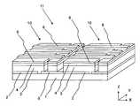
図1は、本発明の一実施形態に係る半導体層の製造方法および本発明の一実施形態に係る光電変換装置の製造方法を用いて作製した光電変換装置を示す斜視図であり、図2はこの光電変換装置の断面図である。なお、図1〜図7には、光電変換セル10の配列方向(図1の図面視左右方向)をX軸方向とする右手系のXYZ座標系が付されている。光電変換装置11は、基板1と、第1の電極層2と、金属カルコゲナイドを含む第1の半導体層3と、第2の半導体層4と、第2の電極層5とを含んでいる。<< (1) Configuration of Photoelectric Conversion Device >>
FIG. 1 is a perspective view showing a photoelectric conversion device manufactured using a method for manufacturing a semiconductor layer according to one embodiment of the present invention and a method for manufacturing a photoelectric conversion device according to one embodiment of the present invention. It is sectional drawing of this photoelectric conversion apparatus. 1 to 7 are provided with a right-handed XYZ coordinate system in which the arrangement direction of photoelectric conversion cells 10 (the horizontal direction in the drawing in FIG. 1) is the X-axis direction. The
第1の半導体層3と第2の半導体層4は導電型が異なっており、第1の半導体層3と第2の半導体層4とで光照射によって生じた正負のキャリアの電荷分離を良好に行うことができる。例えば、第1の半導体層3がp型であれば、第2の半導体層4はn型である。あるいは、第2の半導体層4が、バッファ層と第1の半導体層3とは異なる導電型の半導体層とを含む複数層であってもよい。本実施形態では、第1の半導体層3が一方導電型の光吸収層であり、第2の半導体層4がバッファ層と他方導電型半導体層とを兼ねている例を示している。 The
また、本実施形態における光電変換装置11は第2の電極層5側から光が入射されるものを示しているが、これに限定されず、基板1側から光が入射されるものであってもよい。 Moreover, although the
図1において、光電変換装置11は複数個の光電変換セル10が並べられて形成されている。光電変換セル10は、第1の半導体層3の基板1側に第1の電極層2と離して設けられた第3の電極層6を具備している。そして、第1の半導体層3に設けられた接続導体7によって、第2の電極層5と第3の電極層6とが電気的に接続されている。図1においては、この第3の電極層6は、隣接する光電変換セル10の第1の電極層2が延伸されたものである。この構成により、隣接する光電変換セル10同士が直列接続されている。また、1つの光電変換セル10内において、接続導体7は第1の半導体層3および第2の半導体層4を貫通するように設けられており、第1の電極層2と第2の電極層5とで挟まれた第1の半導体層3と第2の半導体層4とで光電変換が行なわれる。 In FIG. 1, the
基板1は、第1の半導体層3および第2の半導体層4を支持するためのものである。基板1に用いられる材料としては、例えば、ガラス、セラミックス、樹脂および金属等が挙げられる。 The
第1の電極層2および第3の電極層6は、Mo、Al、TiおよびAu等から選ばれる導電体が用いられ、基板1上にスパッタリング法および蒸着法等から選ばれる方法で形成される。 The
第1の半導体層3は金属カルコゲナイドを主に含んだ半導体層である。金属カルコゲナイドとは、金属元素とカルコゲン元素との化合物である。また、カルコゲン元素とは、VI−B族元素(16族元素ともいう)のうちのS、Se、Teをいう。金属カルコゲナイドとしては、例えば、II−VI族化合物、I−III−VI族化合物、I−II−IV−VI族化合物等が挙げられる。 The
II−VI族化合物とは、II−B族元素(12族元素ともいう)とVI−B族元素との化合物であり、例えば、CdTe等が挙げられる。 The II-VI group compound is a compound of a II-B group element (also referred to as a group 12 element) and a VI-B group element, and examples thereof include CdTe.
I−III−VI族化合物とは、I−B族元素(11族元素ともいう)とIII−B族元素(13族元素ともいう)とVI−B族元素との化合物であり、例えば、Cu(In,Ga)Se2(CIGSともいう)、Cu(In,Ga)(Se,S)2(CIGSSともいう)、およびCuInSe2(CISともいう)等が挙げられる。なお、Cu(In,Ga)Se2とは、CuとInとGaとSeとから主に構成された化合物をいう。また、Cu(In,Ga)(Se,S)2とは、CuとInとGaとSeとSとを主成分として含む化合物をいう。The I-III-VI group compound is a compound of a group IB element (also referred to as a
I−II−IV−VI族化合物とは、I−B族元素とII−B族元素とIV−B族元素(14族元素ともいう)とVI−B族元素との化合物であり、例えば、Cu2ZnSn(Se,S)4等が挙げられる。The I-II-IV-VI group compound is a compound of a group I-B element, a group II-B element, a group IV-B element (also referred to as a group 14 element), and a group VI-B element. Cu2 ZnSn (Se, S)4 and the like can be mentioned.
第2の半導体層4は上記第1の半導体層3上に形成されている。本実施形態では、第1の半導体層3が一方導電型の光吸収層であり、第2の半導体層4がバッファ層と他方導電型半導体層とを兼ねている例を示している。リーク電流の低減という観点からは、第2の半導体層4は抵抗率が1Ω・cm以上であってもよい。第2の半導体層4としては、CdS、ZnS、ZnO、In2Se3、In(OH,S)、(Zn,In)(Se,OH)、および(Zn,Mg)O等が挙げられる。第2の半導体層4は、例えばケミカルバスデポジション(CBD)法等で形成される。なお、In(OH,S)とは、InとOHとSとを主成分として含む化合物をいう。(Zn,In)(Se,OH)は、ZnとInとSeとOHとを主成分として含む化合物をいう。(Zn,Mg)Oは、ZnとMgとOとを主成分として含む化合物をいう。第2の半導体層4は、第1の半導体層3の吸収効率を高めるため、第1の半導体層3が吸収する光の波長領域に対して高い光透過性を有するものであってもよい。The
また、第2の半導体層4は、その厚みが10〜200nmである。第2の半導体層4上に第2の電極層5がスパッタリング等で製膜される際のダメージが抑制される観点から言えば、第2の半導体層4の厚みは100〜200nmとされ得る。 The
第2の電極層5は、ITO、ZnO等の0.05〜3.0μmの厚みを有する透明導電膜である。第2の電極層5は、スパッタリング法、蒸着法または化学的気相成長(CVD)法等で形成される。第2の電極層5は、第2の半導体層4よりも抵抗率の低い層であり、第1の半導体層3で生じた電荷を取り出すためのものである。電荷を良好に取り出すという観点からは、第2の電極層5の抵抗率が1Ω・cm未満でシート抵抗が50Ω/□以下であってもよい。なお、第2の電極層5は省略可能であり、第2の半導体層4が第2の電極層5を兼ねてもよい。 The
第2の電極層5としては、第1の半導体層3の吸収効率を高めるため、第1の半導体層3の吸収光に対して高い光透過性を有するものが用いられてもよい。光透過性を高めると同時に光反射ロス低減効果および光散乱効果を高め、さらに光電変換によって生じた電流を良好に伝送するという観点から、第2の電極層5は0.05〜0.5μmの厚さであってもよい。また、第2の電極層5と第2の半導体層4との界面での光反射ロスを低減する観点からは、第2の電極層5と第2の半導体層4の屈折率は略等しくてもよい。 As the
光電変換セル10は、複数個が並べられて電気的に接続され、光電変換装置11となる。隣接する光電変換セル10同士を容易に直列接続するために、図1に示すように、光電変換セル10は、第1の半導体層3の基板1側に第1の電極層2と離して設けられた第3の電極層6を具備している。そして、第1の半導体層3に設けられた接続導体7によって、第2の電極層5と第3の電極層6とが電気的に接続されている。 A plurality of
図1において、接続導体7は、第1の半導体層3、第2の半導体層4および第2の電極層5を貫通(分断)する溝内に、導電性ペースト等の導体が充填されて形成されている。接続導体7はこれに限定されず、第2の電極層5が延長されて形成されていてもよい。なお、接続導体7は第1の半導体層3、第2の半導体層4および第2の電極層5を貫通(分断)する溝内に形成された形態に限らず、これらの積層体の側面に沿って形成されていてもよい。 In FIG. 1, the
また、図1のように、第2の電極層5上に集電電極8が設けられていてもよい。集電電極8は、第2の電極層5の電気抵抗を小さくするためのものである。第2の電極層5上に集電電極8が設けられることにより、第2の電極層5の厚さを薄くして光透過性を高めるとともに第1の半導体層3で発生した電流が効率よく取り出される。その結果、光電変換装置11の発電効率が高められる。 Further, as shown in FIG. 1, a collecting
集電電極8は、例えば、図1に示すように、光電変換セル10の一端から接続導体7にかけて線状に形成されている。これにより、第1の半導体層3の光電変換によって生じた電荷が第2の電極層5を介して集電電極8に集電され、接続導体7を介して隣接する光電変換セル10に良好に伝達される。なお、第2の電極層5が省略され、集電電極8が第2の半導体層4上に形成されていてもよい。 For example, as shown in FIG. 1, the
集電電極8の幅は、第1の半導体層3への光を遮るのを低減するとともに良好な導電性を有するという観点からは、50〜400μmとされ得る。また、集電電極8は、枝分かれした複数の分岐部を有していてもよい。 The width of the
集電電極8は、例えば、Ag等の金属粉を樹脂バインダー等に分散させた金属ペーストがパターン状に印刷され、これが硬化されることによって形成される。 The
<<(2)第1の半導体層の製造方法>>
<(2−1)第1の方法>
金属カルコゲナイドを含む第1の半導体層3は、次のようにして作製することができる。まず、第1の電極層2を有する基板1上に、金属元素、カルコゲン元素、および加熱によって酸素を発生する物質(以下では、加熱によって酸素を発生する物質を酸素発生剤という)を含む皮膜を形成する。皮膜は、金属元素、カルコゲン元素、酸素発生剤および溶媒を含む液状の半導体原料を、例えば、スピンコータ、スクリーン印刷、ディッピング、スプレー、またはダイコータ等の塗布法によって第1の電極層2上に膜状に被着し、溶媒を乾燥によって除去することにより形成することができる。なお、上記皮膜形成を複数回繰り返して複数層の皮膜の積層体としてもよい。<< (2) Manufacturing Method of First Semiconductor Layer >>
<(2-1) First Method>
The
また、上記の酸素発生剤としては、例えば、塩素酸塩類、過塩素酸塩類、亜塩素酸塩類、臭素酸塩類、硝酸塩類、ヨウ素酸塩類、過マンガン酸塩類、重クロム酸塩類、無機過酸化物等がある。 Examples of the oxygen generator include chlorates, perchlorates, chlorites, bromates, nitrates, iodates, permanganates, dichromates, inorganic peroxides. There are things.
このような塩素酸塩類としてはKClO3、NaClO3、NH4ClO3等がある。過塩素酸塩類としてはKClO4、NaClO4、NH4ClO4等がある。亜塩素酸塩類としてはNaClO2等がある。臭素酸塩類としてはKBrO3等がある。硝酸塩類としては、KNO3、NaNO3、NH4NO3等がある。ヨウ素酸塩類としては、NaIO3、KIO3等がある。過マンガン酸塩類としては、KMnO4、NaMnO4・3H2O等がある。重クロム酸塩類としては、K2Cr2O7、(NH4)2Cr2O7等がある。無機過酸化物としては、K2O2、Na2O2、Cu2O2、MgO2、BaO2等がある。Such chlorates include KClO3 , NaClO3 , NH4 ClO3 and the like. Examples of perchlorates include KClO4 , NaClO4 , and NH4 ClO4 . Examples of chlorites include NaClO2 . Examples of bromates include KBrO3 . Examples of nitrates include KNO3 , NaNO3 , NH4 NO3 and the like. Examples of iodates include NaIO3 and KIO3 . Examples of permanganates include KMnO4 and NaMnO4 .3H2 O. Examples of dichromates include K2 Cr2 O7 and (NH4 )2 Cr2 O7 . Inorganic peroxides include K2 O2 , Na2 O2 , Cu2 O2 , MgO2 , BaO2 and the like.
第1の半導体層3の結晶性を高めるという観点からは、酸素発生剤として、KClO3、NaClO3、KClO4、NaClO4、NaClO2、KBrO3、KNO3、NaNO3、NaIO3、KIO3等のアルカリ金属元素を含むものを用いてもよい。From the viewpoint of enhancing the crystallinity of the
酸素発生剤は、第1の半導体層3の半導体特性を良好なものにするという観点から、皮膜に含まれる全金属元素のモル数に対して、1〜50mol%の比率(つまり、皮膜中に含まれる全金属元素を100molとした場合に、酸素発生剤が1〜50mol含まれている)で皮膜中に含有していてもよい。 From the viewpoint of improving the semiconductor characteristics of the
次に、上記の皮膜を、窒素ガス等の不活性ガス雰囲気あるいは水素ガス等の還元ガス雰囲気において50〜600℃に加熱する。これにより、酸素発生剤から酸素が発生するとともに、金属元素とカルコゲン元素とが反応し、金属カルコゲナイドを含む第1の半導体層3が生成する。このとき、加熱によって発生した酸素は、金属カルコゲナイドの結晶化を促進する機能をすると考えられ、良好な金属カルコゲナイド結晶を有する、光電変換効率の高い第1の半導体層3が得られる。これは以下のような現象によるのではないかと考えられる。つまり、皮膜中で酸素を発生させて、効率よく皮膜中に酸素を存在させることによって、一部の金属元素が酸化され、金属元素と金属酸化物が混在した状態となる。そして、金属元素はカルコゲン化が進行し、金属カルコゲナイドから成る小さな粒子が生成する。一方、金属酸化物はすぐにはカルコゲン化が進行せず、一度、金属に変化して流動性を有するものとなり、上記金属カルコゲナイドの小さな粒子同士の隙間に入り込んで緻密な状態になった後にカルコゲン化が進行する。このように緻密な状態でカルコゲン化が進行するため、結晶化が促進するのではないかと考えられる。 Next, the above film is heated to 50 to 600 ° C. in an inert gas atmosphere such as nitrogen gas or a reducing gas atmosphere such as hydrogen gas. As a result, oxygen is generated from the oxygen generator, and the metal element and the chalcogen element react to generate the
なお、皮膜の加熱条件としては、金属カルコゲナイドが結晶化して多結晶体となる温度である400〜600℃に維持する1段階の温度設定であってもよいが、これに限定されない。例えば、比較的低温である50〜350℃に維持して酸素を発生させた後、金属カルコゲナイドが結晶化して多結晶体となる温度である400〜600℃に維持する2段階の温度設定であってもよい。このように、2段階の加熱条件にすると、1段階目に有機成分等の不要な成分を良好に消失させ、その後、2段階目で結晶化を良好に進行させることができるため、第1の半導体層3の結晶性がより良好になる傾向がある。 The heating condition of the film may be one-stage temperature setting at 400 to 600 ° C., which is a temperature at which the metal chalcogenide crystallizes to become a polycrystal, but is not limited thereto. For example, it is a two-stage temperature setting in which oxygen is generated at a relatively low temperature of 50 to 350 ° C., and then maintained at 400 to 600 ° C. that is a temperature at which the metal chalcogenide crystallizes to become a polycrystal. May be. As described above, when the heating conditions are set in two stages, unnecessary components such as organic components can be favorably eliminated in the first stage, and then crystallization can be favorably advanced in the second stage. There is a tendency that the crystallinity of the
また、皮膜のカルコゲン化反応をより促進するという観点から、皮膜の加熱時の雰囲気中にカルコゲン元素を、例えば、硫黄蒸気、硫化水素、セレン蒸気またはセレン化水素等として含有させてもよい。また、雰囲気ガスをすべて硫化水素やセレン化水素のようなカルコゲン元素を含むガスにしてもよい。 Further, from the viewpoint of further promoting the chalcogenization reaction of the film, a chalcogen element may be contained in the atmosphere during heating of the film, for example, as sulfur vapor, hydrogen sulfide, selenium vapor, or hydrogen selenide. Alternatively, the atmosphere gas may be a gas containing a chalcogen element such as hydrogen sulfide or hydrogen selenide.
<(2−2)第2の方法>
金属カルコゲナイドを含む第1の半導体層3は、次のような方法によっても作製され得る。第2の方法では、皮膜中にカルコゲン元素を含んでおらず、カルコゲン元素を外部雰囲気から供給することにより、金属元素のカルコゲン化を行なう。<(2-2) Second method>
The
まず、金属元素および酸素発生剤を含む皮膜を形成する。皮膜は、金属元素、酸素発生剤および溶媒を含む液状の半導体原料を、例えば、スピンコータ、スクリーン印刷、ディッピング、スプレー、またはダイコータ等の塗布法によって第1の電極層2上に膜状に被着し、溶媒を乾燥によって除去することにより形成することができる。なお、上記皮膜形成を複数回繰り返して複数層の皮膜の積層体としてもよい。 First, a film containing a metal element and an oxygen generator is formed. The film is formed by depositing a liquid semiconductor material containing a metal element, an oxygen generator and a solvent on the
上記の金属元素を含む原料および酸素発生剤としては、第1の方法で示されたものと同様のものをそれぞれ用いることができる。皮膜に含まれる全金属元素のモル数に対する酸素発生剤の含有量も第1の方法と同様であってもよい。 As the raw material containing the metal element and the oxygen generator, the same materials as those shown in the first method can be used. The oxygen generator content relative to the number of moles of all metal elements contained in the film may be the same as in the first method.
次に、上記の皮膜を、窒素ガス等の不活性ガス雰囲気あるいは水素ガス等の還元ガス雰囲気において50〜600℃に加熱することによって、上記の酸素発生剤から酸素が発生する。その後、この皮膜を、カルコゲン元素を含む雰囲気中で50〜600℃に加熱することによって、金属カルコゲナイドを含む第1の半導体層3が生成する。この第2の方法も第1の方法と同様に、良好な金属カルコゲナイド結晶を有する、光電変換効率の高い第1の半導体層3が得られる。このように、カルコゲン元素を含まない雰囲気での加熱後、カルコゲン元素を含む雰囲気での加熱を行なう2段階の加熱処理であれば、1段階目に有機成分等の不要な成分を良好に消失させ、その後、2段階目で結晶化を良好に進行させることができるため、第1の半導体層3の結晶性がより良好になる傾向がある。 Next, oxygen is generated from the oxygen generator by heating the film to 50 to 600 ° C. in an inert gas atmosphere such as nitrogen gas or a reducing gas atmosphere such as hydrogen gas. Thereafter, this film is heated to 50 to 600 ° C. in an atmosphere containing a chalcogen element, whereby a
<(2−3)第3の方法>
金属カルコゲナイドを含む第1の半導体層3は、次のような方法によっても作製され得る。第3の方法も、第2の方法と同様、皮膜中にカルコゲン元素を含んでおらず、カルコゲン元素を外部雰囲気から供給することにより、金属元素のカルコゲン化を行なう。<(2-3) Third method>
The
まず、金属元素および酸素発生剤を含む皮膜を形成する。皮膜は、金属元素、酸素発生剤および溶媒を含む液状の半導体原料を、例えば、スピンコータ、スクリーン印刷、ディッピング、スプレー、またはダイコータ等の塗布法によって第1の電極層2上に膜状に被着し、溶媒を乾燥によって除去することにより形成することができる。なお、上記皮膜形成を複数回繰り返して複数層の皮膜の積層体としてもよい。 First, a film containing a metal element and an oxygen generator is formed. The film is formed by depositing a liquid semiconductor material containing a metal element, an oxygen generator and a solvent on the
上記の金属元素および酸素発生剤としては、第1の方法で示されたものと同様のものをそれぞれ用いることができる。皮膜に含まれる全金属元素のモル数に対する酸素発生剤の含有量も第1の方法と同様であってもよい。 As said metal element and oxygen generator, the thing similar to what was shown by the 1st method can be used, respectively. The oxygen generator content relative to the number of moles of all metal elements contained in the film may be the same as in the first method.
次に、上記の皮膜を、カルコゲン元素を含む雰囲気において50〜600℃に加熱することによって、上記の酸素発生剤から酸素が発生するとともに、金属元素とカルコゲン元素とが反応し、金属カルコゲナイドを含む第1の半導体層3が生成する。この第3の方法も第1の方法と同様に、良好な金属カルコゲナイド結晶を有する、光電変換効率の高い第1の半導体層3が得られる。 Next, by heating the above film to 50 to 600 ° C. in an atmosphere containing a chalcogen element, oxygen is generated from the oxygen generator, and the metal element and the chalcogen element react to contain the metal chalcogenide. The
<(2−4)第4の方法>
上記第1〜第3の方法においては、金属元素および酸素発生剤を含む皮膜中の酸素発生剤の含有位置については特に限定していなかったが、第1の半導体層3となる皮膜の厚み方向の一部に酸素発生剤を含むようにしてもよい。以下、第4〜第6の方法においてその製造方法の例を示す。第4〜第6の方法においては、まず、金属元素を含む下部皮膜を、第1の電極層2上に一層あるいは複数の積層体として形成する。そして、この下部皮膜の上に、金属元素および酸素発生剤を含む上部皮膜を、1層あるいは複数層の積層体として形成する。つまり、酸素発生剤は積層された皮膜の上部側に存在するようにする。このような構成により、生成する第1の半導体層3が全体において良好に結晶化が進行しやすくなる。その結果、光電変換効率の面内ばらつきが小さくなり、光電変換効率がさらに高くなる。<(2-4) Fourth Method>
In the first to third methods, the content position of the oxygen generator in the film containing the metal element and the oxygen generator is not particularly limited, but the thickness direction of the film to be the
まず、第4の方法について説明する。第1の電極層2上に形成された下部皮膜は少なくとも金属元素を含んでいる。下部皮膜は、原料溶液を用いた溶液塗布法、スパッタリング法や蒸着法等を用いた薄膜形成方法、あるいは、その他種々の方法によって形成することができる。なお、下部皮膜にはカルコゲン元素が含まれていてもよい。下部皮膜にカルコゲン元素が含まれていない場合、外部雰囲気からカルコゲン元素を供給して金属元素のカルコゲン化を行なえばよい。下部皮膜にカルコゲン元素が含まれている場合は、この下部皮膜に含まれているカルコゲン元素によって金属元素のカルコゲン化を行なうこともでき、外部雰囲気からカルコゲン元素を供給して金属元素のカルコゲン化を行なうこともできる。 First, the fourth method will be described. The lower film formed on the
下部皮膜を、原料溶液を用いた溶液塗布法で形成する場合には、この原料溶液として、上部皮膜の形成に用いる半導体原料のうち、酸素発生剤以外の成分を含むものを用いてもよい。このように上部皮膜と類似した製法で下部皮膜を形成することにより、下部皮膜と上部皮膜とが良好に反応し合い、良好な第1の半導体層3を形成することができる。 When the lower film is formed by a solution coating method using a raw material solution, a semiconductor material used for forming the upper film that includes components other than the oxygen generator may be used as the raw material solution. Thus, by forming the lower film by a manufacturing method similar to the upper film, the lower film and the upper film react well with each other, and a good
この下部皮膜の上に形成された上部皮膜は、金属元素、カルコゲン元素、および酸素発生剤を含む。上部皮膜は、上記第1の方法と同様に、金属元素、カルコゲン元素、酸素発生剤および溶媒を含む液状の半導体用原料を、塗布法によって下部皮膜上に膜状に被着し、溶媒を乾燥によって除去することにより形成することができる。 The upper film formed on the lower film contains a metal element, a chalcogen element, and an oxygen generator. As in the first method, the upper film is formed by depositing a liquid semiconductor raw material containing a metal element, a chalcogen element, an oxygen generator and a solvent on the lower film by a coating method, and drying the solvent. It can form by removing by.
次に、上記の下部皮膜および上部皮膜の積層体を、窒素ガス等の不活性ガス雰囲気、水素ガス等の還元ガス雰囲気、あるいはカルコゲン元素を含む雰囲気において50〜600℃に加熱する。これにより、酸素発生剤から酸素が発生するとともに、金属元素とカルコゲン元素とが反応し、金属カルコゲナイドを含む第1の半導体層3が生成する。 Next, the laminate of the lower film and the upper film is heated to 50 to 600 ° C. in an inert gas atmosphere such as nitrogen gas, a reducing gas atmosphere such as hydrogen gas, or an atmosphere containing a chalcogen element. As a result, oxygen is generated from the oxygen generator, and the metal element and the chalcogen element react to generate the
ここで上記のように、第1の半導体層3となる下部皮膜および上部皮膜を、上層部に酸素発生剤が含まれるように積層した場合は、積層体の上層部で金属酸化物が多く生成し、下層部では比較的金属酸化物が少なくなる。これにより、積層体の下層部や中央部における酸素元素がカルコゲン元素で十分置換されずに残存するのを低減でき、積層体全体においてカルコゲン化が良好に行なわれ、より良好な第1の半導体層3を得ることができる。その結果、光電変換効率の面内ばらつきが小さくなり、光電変換効率がさらに高くなる。なお、上記加熱の工程は、カルコゲン元素を含まない雰囲気で加熱した後、カルコゲン元素を含む雰囲気で加熱する2段階の加熱処理を行なってもよい。このように2段階にすると、1段階目に有機成分等の不要な成分を良好に消失させ、その後、2段階目で結晶化を良好に進行させることができるため、第1の半導体層3の結晶性がより良好になる傾向がある。 Here, as described above, when the lower film and the upper film to be the
<(2−5)第5の方法>
金属カルコゲナイドを含む第1の半導体層3は、次のような方法によっても作製することができる。第5の方法では、上部皮膜中にカルコゲン元素を含んでおらず、カルコゲン元素を外部雰囲気から供給することにより、金属元素のカルコゲン化を行なう。<(2-5) Fifth method>
The
まず、第4の方法と同様に金属元素を含む下部皮膜を形成する。なお、金属カルコゲナイドの形成を良好にするため、下部皮膜にカルコゲン元素を含めておいてもよい。 First, a lower film containing a metal element is formed as in the fourth method. In order to improve the formation of the metal chalcogenide, a chalcogen element may be included in the lower film.
次に、この下部皮膜の上に金属元素および酸素発生剤を含む上部皮膜を形成する。上部皮膜は、上記第2の方法と同様に、金属元素、酸素発生剤および溶媒を含む液状の半導体原料を、塗布法によって下部皮膜上に膜状に被着し、溶媒を乾燥によって除去することにより形成することができる。 Next, an upper film containing a metal element and an oxygen generator is formed on the lower film. As in the second method, the upper film is formed by depositing a liquid semiconductor raw material containing a metal element, an oxygen generator and a solvent on the lower film by a coating method, and removing the solvent by drying. Can be formed.
次に、上記の下部皮膜および上部皮膜の積層体を、窒素ガス等の不活性ガス雰囲気あるいは水素ガス等の還元ガス雰囲気において50〜600℃に加熱する。これにより、上記の酸素発生剤から酸素が発生する。その後、この下部皮膜および上部皮膜の積層体を、カルコゲン元素を、例えば硫黄蒸気、硫化水素、セレン蒸気またはセレン化水素等として含む雰囲気中で50〜600℃に加熱することによって、金属カルコゲナイドを含む第1の半導体層3が生成する。この第5の方法も第4の方法と同様に、積層体全体においてカルコゲン化が良好に行なわれ、より良好な第1の半導体層3を得ることができる。その結果、光電変換効率の面内ばらつきが小さくなり、光電変換効率がさらに高くなる。 Next, the laminate of the lower film and the upper film is heated to 50 to 600 ° C. in an inert gas atmosphere such as nitrogen gas or a reducing gas atmosphere such as hydrogen gas. Thereby, oxygen is generated from the oxygen generator. Thereafter, the laminated body of the lower film and the upper film is heated to 50 to 600 ° C. in an atmosphere containing a chalcogen element as, for example, sulfur vapor, hydrogen sulfide, selenium vapor, hydrogen selenide or the like, thereby including metal chalcogenide. The
<(2−6)第6の方法>
金属カルコゲナイドを含む第1の半導体層3は、次のような方法によっても作製することができる。第6の方法も、第5の方法と同様、上部皮膜中にカルコゲン元素を含んでおらず、カルコゲン元素を外部雰囲気から供給することにより、金属元素のカルコゲン化を行なう。<(2-6) Sixth Method>
The
まず、第4の方法と同様に金属元素を含む下部皮膜を形成する。なお、金属カルコゲナイドの形成を良好にするため、下部皮膜にカルコゲン元素を含めておいてもよい。 First, a lower film containing a metal element is formed as in the fourth method. In order to improve the formation of the metal chalcogenide, a chalcogen element may be included in the lower film.
次に、この下部皮膜の上に、金属元素および酸素発生剤を含む上部皮膜を形成する。上部皮膜は、上記第2の方法と同様に、金属元素、酸素発生剤および溶媒を含む液状の半導体原料を、塗布法によって下部皮膜上に膜状に被着し、溶媒を乾燥によって除去することにより形成することができる。 Next, an upper film containing a metal element and an oxygen generator is formed on the lower film. As in the second method, the upper film is formed by depositing a liquid semiconductor raw material containing a metal element, an oxygen generator and a solvent on the lower film by a coating method, and removing the solvent by drying. Can be formed.
次に、上記の下部皮膜および上部皮膜の積層体を、カルコゲン元素を、例えば硫黄蒸気、硫化水素、セレン蒸気またはセレン化水素等として含む雰囲気において50〜600℃に加熱することによって、上記の酸素発生剤から酸素が発生するとともに、金属元素とカルコゲン元素とが反応し、金属カルコゲナイドを含む第1の半導体層3が生成する。この第6の方法も第4の方法と同様に、積層体全体においてカルコゲン化が良好に行なわれ、より良好な第1の半導体層3を得ることができる。その結果、光電変換効率の面内ばらつきが小さくなり、光電変換効率がさらに高くなる。 Next, the laminated body of the lower coating and the upper coating is heated to 50 to 600 ° C. in an atmosphere containing a chalcogen element as, for example, sulfur vapor, hydrogen sulfide, selenium vapor, or hydrogen selenide. Oxygen is generated from the generator, and the metal element and the chalcogen element react to generate the
<<(3)半導体原料の製造方法>>
上記第1の半導体層の製造方法で用いた半導体原料の製造方法について詳細に説明する。なお、第1の半導体層の製造方法において、半導体層となる皮膜の形成方法としては、下記に示すような液状の半導体原料を塗布して皮膜を形成する方法に限定されず、溶媒を含まない固体状の半導体原料を用いた乾式の薄膜形成方法を適用してもよい。<< (3) Manufacturing Method of Semiconductor Raw Material >>
The manufacturing method of the semiconductor raw material used by the manufacturing method of the said 1st semiconductor layer is demonstrated in detail. In the first method for producing a semiconductor layer, the method for forming a film to be a semiconductor layer is not limited to the method for forming a film by applying a liquid semiconductor raw material as shown below, and does not include a solvent. A dry thin film forming method using a solid semiconductor raw material may be applied.
半導体原料は、上記第2の方法、第3の方法、第5の方法および第6の方法に示されるように、金属元素および酸素発生剤が溶媒中に分散または溶解されている(以下では、金属元素、酸素発生剤および溶媒を含む半導体原料を第1の半導体原料という)。あるいは、上記第1の方法および第4の方法に示されるように、金属元素および酸素発生剤に加えて、さらにカルコゲン元素も溶媒中に分散または溶解されていてもよい(以下では、金属元素、カルコゲン元素、酸素発生剤および溶媒を含む半導体原料を第2の半導体原料という)。 As shown in the second method, the third method, the fifth method, and the sixth method, the semiconductor raw material has a metal element and an oxygen generator dispersed or dissolved in a solvent (hereinafter, A semiconductor raw material containing a metal element, an oxygen generator and a solvent is referred to as a first semiconductor raw material). Alternatively, as shown in the first method and the fourth method, in addition to the metal element and the oxygen generator, a chalcogen element may be further dispersed or dissolved in a solvent (hereinafter referred to as a metal element, A semiconductor raw material containing a chalcogen element, an oxygen generator and a solvent is referred to as a second semiconductor raw material).
第1の半導体原料は、金属元素を含む原料および酸素発生剤を溶媒中に分散または溶解することによって作製できる。また、第2の半導体原料は、金属元素を含む原料および酸素発生剤に加えて、カルコゲン元素を含む原料を溶媒中に分散または溶解することによって作製できる。 The first semiconductor material can be manufactured by dispersing or dissolving a material containing a metal element and an oxygen generator in a solvent. The second semiconductor material can be manufactured by dispersing or dissolving a material containing a chalcogen element in a solvent in addition to a material containing a metal element and an oxygen generator.
上記の金属元素を含む原料としては、金属または金属化合物を用いることができる。このような金属としては、金属単体または合金が挙げられる。また、金属化合物としては、非酸化物系の化合物が挙げられ、例えば、金属塩または金属錯体がある。 As a raw material containing the above metal element, a metal or a metal compound can be used. As such a metal, a metal simple substance or an alloy is mentioned. Examples of the metal compound include non-oxide compounds, such as metal salts or metal complexes.
上記のカルコゲン元素を含む原料としては、カルコゲン元素単体またはカルコゲン化合物を用いることができる。このようなカルコゲン化合物としては、カルコゲン元素を含む有機化合物またはカルコゲン元素を含む無機化合物が用いられる。 As the raw material containing the chalcogen element, a chalcogen element alone or a chalcogen compound can be used. As such a chalcogen compound, an organic compound containing a chalcogen element or an inorganic compound containing a chalcogen element is used.
上記の溶媒としては、金属元素や酸素発生剤等の原料が溶解または分散可能なものであればよく、特に限定されない。溶媒としては、例えばピリジンやアニリン等の塩基性溶媒やアルコール等が挙げられる。 The solvent is not particularly limited as long as a raw material such as a metal element or an oxygen generator can be dissolved or dispersed. Examples of the solvent include basic solvents such as pyridine and aniline, alcohols, and the like.
なお、上記の金属元素を含む原料およびカルコゲン元素を含む原料は、金属元素を含む原料とカルコゲン元素を含む原料との混合物である必要はなく、金属元素とカルコゲン元素との化合物となったものも含む。反応性を高くして第1の半導体層3の結晶化を良好にするという観点からは、金属元素とカルコゲン元素とが1つの錯体分子中に存在する錯体化合物を用いてもよい。このような錯体化合物としては、例えば、金属元素に有機カルコゲン化合物が配位したものがある。 The raw material containing the metal element and the raw material containing the chalcogen element do not have to be a mixture of the raw material containing the metal element and the raw material containing the chalcogen element, and may be a compound of the metal element and the chalcogen element. Including. From the viewpoint of increasing the reactivity and improving the crystallization of the
有機カルコゲン化合物とは、カルコゲン元素を有する有機化合物であり、炭素元素とカルコゲン元素との共有結合を有する有機化合物である。有機カルコゲン化合物は、例えば、チオール、スルフィド、ジスルフィド、チオフェン、スルホキシド、スルホン、チオケトン、スルホン酸、スルホン酸エステル、スルホン酸アミド、セレノール、セレニド、ジセレニド、セレノキシド、セレノン、テルロール、テルリド、ジテルリド等がある。特に、配位力が高く金属元素と安定な錯体を形成しやすいという観点からは、チオール、スルフィド、ジスルフィド、セレノール、セレニド、ジセレニド、テルロール、テルリド、ジテルリドを用いてもよい。 An organic chalcogen compound is an organic compound having a chalcogen element, and is an organic compound having a covalent bond between a carbon element and a chalcogen element. Examples of the organic chalcogen compound include thiol, sulfide, disulfide, thiophene, sulfoxide, sulfone, thioketone, sulfonic acid, sulfonic acid ester, sulfonic acid amide, selenol, selenide, diselenide, selenoxide, selenone, tellurol, telluride, ditelluride and the like. . In particular, thiol, sulfide, disulfide, selenol, selenide, diselenide, tellurol, telluride, and ditelluride may be used from the viewpoint of high coordination ability and easy formation of a stable complex with a metal element.
金属元素に有機カルコゲン化合物が配位した錯体化合物としては、例えば、金属元素がIII−B族元素であり、III−B元素をM、有機カルコゲン化合物をE、任意の陽イオンをAとした場合、A+[ME4]−(以下、III族錯体という)である。このようなIII族錯体A+[ME4]−は、III−B族元素の塩M3+B−3(Bは任意の陰イオンである)と有機カルコゲン化合物の塩A+E−とを反応させることによって得ることができるが、この反応の際の副生成物として、A+B−が生成する。この副生成物A+B−は、洗浄によって除去してもよいが、副生成物A+B−が酸素発生剤となるような陰イオンBを選択することにより、この副生成物A+B−を酸素発生剤として用いることができる。これにより、洗浄工程が不要となり工程を簡略化できる。特に、陽イオンAがアルカリ金属元素であれば、このアルカリ金属元素も半導体層形成時の結晶化反応を促進する機能を有するため、このアルカリ金属元素を含む副生成物を有効に利用することができる。As a complex compound in which an organic chalcogen compound is coordinated to a metal element, for example, when the metal element is a III-B group element, the III-B element is M, the organic chalcogen compound is E, and any cation is A , A+ [ME4 ]− (hereinafter referred to as group III complex). + Such group III complexA[ME 4]- are, III-B
具体的には、陽イオンA+をNa+、陰イオンB−をClO4−、III−B族元素をIn、有機カルコゲン化合物Eをフェニルセレノールとした場合に、Na(SePh)とIn(ClO4)3とを反応させることにより、金属元素に有機カルコゲン化合物が配位した錯体化合物であるNa[In(SePh)4]が生成するとともに、副生成物として酸素発生剤であるNaClO4が生成する。同様に、Na(SePh)とGa(ClO4)3とを反応させることにより、Na[Ga(SePh)4]が生成するとともに、副生成物としてNaClO4が生成する。Specifically, when the cation A+ is Na+ , the anion B− is ClO4− , the III-B group element is In, and the organic chalcogen compound E is phenyl selenol, Na (SePh) and In ( By reacting with ClO4 )3 , Na [In (SePh)4 ], which is a complex compound in which an organic chalcogen compound is coordinated to a metal element, is generated, and NaClO4 that is an oxygen generator is formed as a by-product. Generate. Similarly, by reacting Na (SePh) and Ga (ClO4 )3 , Na [Ga (SePh)4 ] is generated and NaClO4 is generated as a by-product.
第1の半導体層3に含まれる金属カルコゲナイドが複数種の金属元素を含む場合には、反応性を高くして第1の半導体層3の結晶化を良好にするという観点からは、半導体原料が、複数種の金属元素とカルコゲン元素とが1つの錯体分子中に存在する錯体化合物を有していてもよい。このような錯体化合物としては、例えば、第1の半導体層3に含まれる金属カルコゲナイドがI−III−VI族化合物の場合、I−B族元素とIII−B族元素とカルコゲン元素(VI−B族元素)とが1つの錯体分子中に存在する錯体化合物が用いられる。このような錯体化合物の具体例としては、I−B元素をMIとし、III−B元素をMとし、ルイス塩基をLとし、有機カルコゲン化合物をEとしたときに、構造式(1)等が挙げられる。In the case where the metal chalcogenide contained in the

なお、ルイス塩基は非共有電子対を有する化合物である。ルイス塩基としては、非共有電子対を有するV−B族元素(15族元素ともいう)を具備した官能基や非共有電子対を有するVI−B族元素を具備した官能基を有する化合物が挙げられる。ルイス塩基の具体例としては、P(C6H5)3、As(C6H5)3、N(C6H5)3等がある。A Lewis base is a compound having an unshared electron pair. Examples of the Lewis base include a compound having a functional group having a VB group element having an unshared electron pair (also referred to as a Group 15 element) or a functional group having a VI-B group element having an unshared electron pair. It is done. Specific examples of the Lewis base include P (C6 H5 )3 , As (C6 H5 )3 , and N (C6 H5 )3 .
構造式(1)で示される錯体化合物の具体例としては、構造式(2)や構造式(3)のような化合物が挙げられる。なお、これらの構造式において、Phはフェニル基を意味する。 Specific examples of the complex compound represented by the structural formula (1) include compounds such as the structural formula (2) and the structural formula (3). In these structural formulas, Ph means a phenyl group.
このような構造式(1)で示される錯体化合物は、ルイス塩基Lがトリフェニルフォスフィンであり、有機カルコゲン化合物Eがフェニルセレノールの場合であれば、例えば、I−B族元素の化合物である{P(C6H5)3}2MI(CH3CN)2・PF6と、上述したIII族錯体であるA+[M(SePh)4]−とを反応させることによって作製することができる。III−B族元素MがInであれば、構造式(2)で示される錯体化合物が得られ、III−B族元素MがGaであれば、構造式(3)で示される錯体化合物が得られる。When the Lewis base L is triphenylphosphine and the organic chalcogen compound E is phenyl selenol, the complex compound represented by the structural formula (1) is, for example, a compound of an IB group element. It is produced by reacting a certain {P (C6 H5 )3 }2 MI (CH3 CN)2 .PF6 with the group III complex A+ [M (SePh)4 ]− described above. be able to. If the III-B group element M is In, a complex compound represented by the structural formula (2) is obtained. If the III-B group element M is Ga, a complex compound represented by the structural formula (3) is obtained. It is done.
ここでIII族錯体であるA+[M(SePh)4]−は、上述したように、その作製工程において生成する副生成物が酸素発生剤となるような陰イオンBを選択することにより、この副生成物を酸素発生剤として用いることができる。これにより、洗浄工程が不要となり、工程の簡略化が可能となる。特に、陽イオンAがアルカリ金属元素であれば、このアルカリ金属元素も半導体層形成時の結晶化反応を促進する機能を有するため、このアルカリ金属元素を含む副生成物を有効に利用することができる。Here, the group III complex A+ [M (SePh)4 ]− is selected by selecting an anion B such that a by-product generated in the production process becomes an oxygen generator, as described above. This by-product can be used as an oxygen generator. This eliminates the need for a cleaning process and simplifies the process. In particular, if the cation A is an alkali metal element, the alkali metal element also has a function of accelerating the crystallization reaction during the formation of the semiconductor layer. Therefore, it is possible to effectively use the by-product containing the alkali metal element. it can.
<<(4)光電変換装置の製造方法>>
図3〜図7は、光電変換装置11の製造途中の様子をそれぞれ模式的に示す断面図または斜視図である。なお、図3〜図7で示される各断面図は、図2で示された断面に対応する部分の製造途中の様子を示す。<< (4) Manufacturing Method of Photoelectric Conversion Device >>
3 to 7 are cross-sectional views or perspective views schematically showing the process of manufacturing the
まず、洗浄された基板1の略全面に、スパッタリング法等を用いて、Mo等からなる第1の電極層2を成膜する。そして、第1の電極層2の上面のうちのY方向に沿った直線状の形成対象位置からその直下の基板1の上面にかけて、第1溝部P1を形成する。第1溝部P1は、例えば、YAGレーザー等によるレーザー光を走査しつつ形成対象位置に照射することで溝加工を行なう、スクライブ加工によって形成することができる。図3は、第1溝部P1を形成した後の状態を示す図である。 First, the
第1溝部P1を形成した後、第1の電極層2の上に、第1の半導体層3を形成する。第1の半導体層3は、上述した第1の半導体層3の製造方法によって形成する。図4は、第1の半導体層3を形成した後の状態を示す図である。 After forming the first groove P <b> 1, the
第1の半導体層3を形成した後、第1の半導体層3の上に、第2の半導体層4および第2の電極層5を順に形成する。 After forming the
第2の半導体層4は、溶液成長法(CBD法ともいう)によって形成することができる。例えば、酢酸カドミウムとチオ尿素とをアンモニア水に溶解し、これに第1の半導体層3の形成まで行なった基板1を浸漬することで、第1の半導体層3の上にCdSを含む第2の半導体層4を形成することができる。 The
第2の電極層5は、例えば、Snが含まれた酸化インジウム(ITO)等を主成分とする透明導電膜であり、スパッタリング法、蒸着法またはCVD法等で形成することができる。図5は、第2の半導体層4および第2の電極層5を形成した後の状態を示す図である。 The
上部電極層5を形成した後、第2の電極層5の上面のうちのY方向に沿った直線状の形成対象位置からその直下の第1の電極層2(図2の第3の電極層6に相当する部分)の上面にかけて、第2溝部P2を形成する。第2溝部P2は、例えば、スクライブ針を用いたメカニカルスクライビングによって形成できる。図6は、第2溝部P2を形成した後の状態を示す図である。第2溝部P2は、第1溝部P1よりも若干X方向(図中では+X方向)にずれた位置に形成される。 After the
第2溝部P2を形成した後、集電電極8および接続導体7を形成する。集電電極8および接続導体7については、例えば、Ag等の金属粉を樹脂バインダー等に分散させた導電性を有するペースト(導電ペーストともいう)を、所望のパターンを描くように印刷することで形成できる。図7は、集電電極8および接続導体7を形成した後の状態を示す図である。 After forming the second groove P2, the
集電電極8および接続導体7を形成した後、第2の電極層5の上面のうちの直線状の形成対象位置からその直下の第1の電極層2の上面にかけて、第3溝部P3を形成する。第3溝部P3の幅は、例えば、40〜1000μm程度とすることができる。また、第3溝部P3は、第2溝部P2と同様に、メカニカルスクライビングによって形成することができる。このようにして、第3溝部P3の形成によって、図1および図2で示された光電変換装置11が製作されたことになる。 After forming the
なお、本発明は上述の実施形態に限定されるものではなく、本発明の要旨を逸脱しない範囲内で種々の変更が施されることは何等差し支えない。 Note that the present invention is not limited to the above-described embodiment, and various modifications may be made without departing from the scope of the present invention.
本発明の実施形態にかかる半導体層の製造方法および光電変換装置の製造方法について、以下のようにして評価した。本実施例においては、半導体層に含まれる金属カルコゲナイドとしてCIGSを用いた。 The semiconductor layer manufacturing method and the photoelectric conversion device manufacturing method according to the embodiment of the present invention were evaluated as follows. In this example, CIGS was used as the metal chalcogenide contained in the semiconductor layer.
<半導体原料の作製>
[a1]10ミリモル(mmol)のCu(CH3CN)4・BF4と、20mmolのP(C6H5)3とを、100mlのメタノールに溶解した後、30℃における3時間の攪拌によって第1錯体溶液を調製した。<Production of semiconductor raw materials>
[A1] 10 mmol (mmol) of Cu (CH3 CN)4 .BF4 and 20 mmol of P (C6 H5 )3 were dissolved in 100 ml of methanol, and then stirred at 30 ° C. for 3 hours. A first complex solution was prepared.
[a2]40mmolのナトリウムメトキシド(CH3ONa)と、有機カルコゲン化合物である40mmolのフェニルセレノール(C6H5SeH)とを、300mlのメタノールに溶解し、さらに、7mmolのInCl3と3mmolのGaCl3とを溶解した後、室温における2時間の攪拌によって第2錯体溶液を調製した。[A2] 40 mmol sodium methoxide (CH3 ONa) and 40 mmol phenyl selenol (C6 H5 SeH) which is an organic chalcogen compound are dissolved in 300 ml methanol, and further 7 mmol InCl3 and 3 mmol are dissolved. after dissolving and GaCl3, to prepare a second complex solution by stirring for 2 hours at room temperature.
[a3]上記第1錯体溶液に対して、上記第2錯体溶液を1分間に10mlの速度で滴下することによって析出物が生じた。この析出物をろ過し、室温で乾燥することによって、構造式1および構造式2に示すような単一源錯体の混合物を得た。 [A3] Precipitates were formed by dropping the second complex solution at a rate of 10 ml per minute with respect to the first complex solution. The precipitate was filtered and dried at room temperature to obtain a mixture of single source complexes as shown in
上記工程で作製された単一源錯体の混合物を有機溶媒であるピリジンに溶解することによって、液状の半導体原料1を作製した。さらにこの半導体原料1の一部を取り出し、この取り出した半導体原料1に過塩素酸ナトリウム(NaClO4)を添加することによって、液状の半導体原料2を作製した。なお、この半導体原料2に含まれるNaClO4のモル数は、半導体原料2に含まれるCuのモル数に対して2%とした。The liquid semiconductor
<評価試料1に係る第1の半導体層の作製>
次に、ガラスを主に含む、一辺が100mmの正方形の主面を有する基板を用意した。そして、この基板の主面に、Mo等を含む第1の電極層を成膜した。そして、窒素ガスの雰囲気下において第1の電極層の上に上記の半導体原料2をブレード法によって塗布し、窒素ガスの雰囲気下において300℃で10分間加熱することによって皮膜を形成した。<Production of First Semiconductor Layer According to
Next, a substrate mainly including glass and having a square main surface with a side of 100 mm was prepared. And the 1st electrode layer containing Mo etc. was formed into a film on the main surface of this board | substrate. Then, the semiconductor
そして、この皮膜を、分圧比で100ppmvのSe蒸気を含む水素ガス雰囲気下において、550℃で1時間加熱することにより、主にCIGSから成る評価試料1に係る第1の半導体層を形成した。 Then, this film was heated at 550 ° C. for 1 hour in a hydrogen gas atmosphere containing Se vapor having a partial pressure ratio of 100 ppmv, thereby forming a first semiconductor layer related to the
<比較試料1に係る第1の半導体層の作製>
上記評価試料1に係る第1半導体層の作製において、皮膜を、過塩素酸ナトリウムを含まない半導体原料1に代えて作製した。そして、この皮膜を100ppmvのSe蒸気を含む水素ガス雰囲気下において、550℃で1時間加熱することにより、主にCIGSから成る比較試料1に係る第1の半導体層を形成した。<Fabrication of First Semiconductor Layer According to
In the production of the first semiconductor layer according to the
<光電変換装置の作製>
次に、上述のように作製された評価試料1および比較試料1に係る各第1の半導体層の上に、それぞれ、第2の半導体層と第2の電極層とを順に形成して光電変換装置を作製した。<Production of photoelectric conversion device>
Next, a second semiconductor layer and a second electrode layer are sequentially formed on each of the first semiconductor layers according to the
具体的には、塩化インジウムおよびチオ尿素が溶解された水溶液に、主にCIGSから成る第1の半導体層が形成された基板を浸漬することで、第1の半導体層の上に厚さが50nmのIn2S3を含む第2の半導体層を形成した。さらに、この第2の半導体層の上に、スパッタリング法によってAlがドープされた酸化亜鉛を含む透明の導電膜(第2の電極層)を形成した。Specifically, by immersing the substrate on which the first semiconductor layer mainly made of CIGS is formed in an aqueous solution in which indium chloride and thiourea are dissolved, a thickness of 50 nm is formed on the first semiconductor layer. Asecond semiconductor layer containing In2 S3 was formed. Further, a transparent conductive film (second electrode layer) containing zinc oxide doped with Al was formed on the second semiconductor layer by a sputtering method.
<光電変換装置における光電変換効率の測定>
作製した各光電変換装置の光電変換効率を、定常光ソーラーシミュレーターを用いて測定した。ここでは、光電変換装置の受光面に対する光の照射強度が100mW/cm2であり且つエアマス(AM)が1.5である条件下で光電変換効率を測定した。なお、光電変換効率は、光電変換装置において太陽光のエネルギーが電気エネルギーに変換される割合を示し、ここでは、光電変換装置から出力される電気エネルギーの値を、光電変換装置に入射される太陽光のエネルギーの値で割り、100をかけることで導出した。<Measurement of photoelectric conversion efficiency in photoelectric conversion device>
The photoelectric conversion efficiency of each produced photoelectric conversion apparatus was measured using a stationary light solar simulator. Here, the photoelectric conversion efficiency was measured under conditions where the light irradiation intensity on the light receiving surface of the photoelectric conversion device was 100 mW / cm2 and the air mass (AM) was 1.5. Note that the photoelectric conversion efficiency indicates the rate at which sunlight energy is converted into electric energy in the photoelectric conversion device. Here, the value of the electric energy output from the photoelectric conversion device is the solar energy incident on the photoelectric conversion device. Divided by the value of light energy and multiplied by 100.
その結果、比較試料1に係る第1の半導体層を用いて作製した光電変換装置における光電変換効率は11.0%であったのに対し、評価試料1に係る第1の半導体層を用いて作製した光電変換装置における光電変換効率は11.5%であった。 As a result, the photoelectric conversion efficiency in the photoelectric conversion device manufactured using the first semiconductor layer according to the
以上の結果から、酸素発生剤を含む半導体原料2で皮膜を形成した場合(評価試料1に係る第1の半導体層)は、酸素発生剤を含まない半導体原料1で皮膜を形成した場合(比較試料1に係る第1の半導体層)よりも、光電変換効率が高くなっていることがわかった。 From the above results, when the film is formed with the semiconductor
本発明の実施形態にかかる半導体層の製造方法および光電変換装置の製造方法について、以下のようにして評価した。本実施例においては半導体層に含まれる金属カルコゲナイドとしてCIGSを用いた。 The semiconductor layer manufacturing method and the photoelectric conversion device manufacturing method according to the embodiment of the present invention were evaluated as follows. In this example, CIGS was used as the metal chalcogenide contained in the semiconductor layer.
<半導体原料の作製>
実施例1と同様にして、過塩素酸ナトリウムを含まない半導体原料1と、過塩素酸ナトリウムを含む半導体原料2とを用意した。<Production of semiconductor raw materials>
In the same manner as in Example 1, a semiconductor
<評価試料2に係る第1の半導体層の作製>
次に、ガラスを主に含む、長辺が800mmで短辺が500mmの長方形の主面を有する基板を用意した。そして、この基板の主面に、Mo等を含む第1の電極層を成膜した。そして、窒素ガスの雰囲気下において第1の電極層の上に上記の半導体原料1をブレード法によって塗布し、窒素ガスの雰囲気下において300℃で10分間加熱することによって皮膜を形成した。この塗布および加熱工程を合計5回繰り返すことによって、5層の皮膜の積層体1を作製した。<Production of First Semiconductor Layer According to
Next, a substrate having a rectangular main surface mainly containing glass and having a long side of 800 mm and a short side of 500 mm was prepared. And the 1st electrode layer containing Mo etc. was formed into a film on the main surface of this board | substrate. Then, the semiconductor
さらに、この5層の皮膜の積層体1の上に上記の半導体原料2をブレード法によって塗布し、窒素ガスの雰囲気下において300℃で10分間加熱することにより、合計が6層の皮膜の積層体2を作製した。 Further, the semiconductor
そして、この6層の皮膜の積層体2を、分圧比で100ppmvのSe蒸気を含む水素ガス雰囲気下において、550℃で1時間加熱することにより、主にCIGSから成る評価試料2に係る第1の半導体層を形成した。 Then, the
<評価試料3に係る第1の半導体層の作製>
上記評価試料2に係る第1半導体層の作製において、6層の皮膜の積層体を、すべて半導体原料2を用いて作製した。そして、この6層の皮膜の積層体を100ppmvのSe蒸気を含む水素ガス雰囲気下において、550℃で1時間加熱することにより、主にCIGSから成る評価試料3に係る第1の半導体層を形成した。<Fabrication of First Semiconductor Layer According to
In the production of the first semiconductor layer according to the
<比較試料2に係る第1の半導体層の作製>
上記評価試料2に係る第1半導体層の作製において、6層の皮膜の積層体を、すべて半導体原料1を用いて作製した。そして、この6層の皮膜の積層体を100ppmvのSe蒸気を含む水素ガス雰囲気下において、550℃で1時間加熱することにより、主にCIGSから成る比較試料2に係る第1の半導体層を形成した。<Fabrication of First Semiconductor Layer According to
In the production of the first semiconductor layer according to the
<光電変換装置の作製>
次に、上述のように作製された評価試料2、評価試料3および比較試料2に係る各第1の半導体層の上に、それぞれ、第2の半導体層と第2の電極層とを順に形成して光電変換装置を作製した。<Production of photoelectric conversion device>
Next, a second semiconductor layer and a second electrode layer are sequentially formed on each of the first semiconductor layers according to the
具体的には、アンモニア水に酢酸カドミウムおよびチオ尿素が溶解された溶液に、主にCIGSから成る第1の半導体層が形成された基板を浸漬することで、第1の半導体層の上に厚さが50nmのCdSを含む第2の半導体層を形成した。さらに、この第2の半導体層の上に、スパッタリング法によってAlがドープされた酸化亜鉛を含む透明の導電膜(第2の電極層)を形成した。 Specifically, by immersing the substrate on which the first semiconductor layer mainly made of CIGS is formed in a solution in which cadmium acetate and thiourea are dissolved in ammonia water, the thickness is increased on the first semiconductor layer. A second semiconductor layer containing CdS having a thickness of 50 nm was formed. Further, a transparent conductive film (second electrode layer) containing zinc oxide doped with Al was formed on the second semiconductor layer by a sputtering method.
<光電変換装置における光電変換効率の測定>
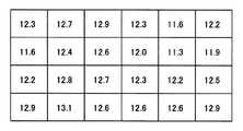
作製した各光電変換装置を図8〜10に示すように、長辺方向に6等分し、さらに短辺方向に4等分して24個の光電変換装置(以下、分割光電変換装置ともいう)に分割した。そして、各分割光電変換装置の光電変換効率を実施例1と同様にして測定した。<Measurement of photoelectric conversion efficiency in photoelectric conversion device>
As shown in FIGS. 8 to 10, each of the produced photoelectric conversion devices is divided into six equal parts in the long side direction and further divided into four equal parts in the short side direction (hereinafter also referred to as divided photoelectric conversion devices). ). And the photoelectric conversion efficiency of each division | segmentation photoelectric conversion apparatus was measured like Example 1. FIG.
図8は評価試料2に係る第1の半導体層を用いて作製された光電変換装置における光電変換効率(%)の面内分布を示す図である。図8に示す結果から、光電変換装置の光電変換効率の平均値、すなわち24個の分割光電変換装置の光電変換効率の平均値は12.4%であり、標準偏差σは0.45であった。また、図9は、評価試料3に係る第1の半導体層を用いて作製された光電変換装置における光電変換効率の面内分布を示す図である。図9の結果から、光電変換効率の平均値は11.5%であり標準偏差σは0.71であった。また、図10は比較試料2に係る第1の半導体層を用いて作製された光電変換装置における光電変換効率の面内分布を示す図である。図10の結果から、光電変換効率の平均値は11.2%であり標準偏差σは0.69であった。 FIG. 8 is a diagram showing an in-plane distribution of photoelectric conversion efficiency (%) in a photoelectric conversion device manufactured using the first semiconductor layer according to the
以上の結果から、酸素発生剤を含む半導体原料2で形成した皮膜を含む場合(評価試料2に係る第1の半導体層および評価試料3に係る第1の半導体層)は、酸素発生剤を含まない半導体原料1で形成した皮膜のみの場合(比較試料2に係る第1の半導体層)よりも、光電変換効率が高くなっていることがわかった。 From the above results, in the case of including a film formed of the semiconductor
特に、酸素発生剤を含む半導体原料2を最上層の皮膜形成のみに用いた場合(評価試料2に係る第1の半導体層)は、光電変換効率の面内ばらつきが非常に小さくなり、平均光電変換効率がさらに高くなっていることがわかった。 In particular, when the semiconductor
1:基板
2:第1の電極層
3:第1の半導体層(金属カルコゲナイドを含む半導体層)
4:第2の半導体層
5:第2の電極層
6:第3の電極層
7:接続導体
8:集電電極
10:光電変換セル
11:光電変換装置1: Substrate 2: First electrode layer 3: First semiconductor layer (semiconductor layer containing metal chalcogenide)
4: Second semiconductor layer 5: Second electrode layer 6: Third electrode layer 7: Connection conductor 8: Current collecting electrode 10: Photoelectric conversion cell 11: Photoelectric conversion device
Claims (8)
Translated fromJapanese該皮膜を加熱して前記物質から酸素を発生させる工程と、
前記金属元素とカルコゲン元素とを反応させることによって、前記皮膜から金属カルコゲナイドを含む半導体層を形成する工程とを具備し、
前記酸素を発生する物質としてアルカリ金属元素を含むものを用いることを特徴とする半導体層の製造方法。Forming a film containing a metal element and a substance that generates oxygen by heating;
Heating the film to generate oxygen from the substance;
Forming a semiconductor layer containing metal chalcogenide from the coating by reacting the metal element with the chalcogen element,
A method for manufacturing a semiconductor layer,wherein a substance containing an alkali metal element is used as the substance that generates oxygen .
該下部皮膜の上に金属元素および加熱によって酸素を発生する物質を含む上部皮膜を形成する工程と、
前記上部皮膜を加熱して前記物質から酸素を発生させる工程と、
カルコゲン元素と前記下部皮膜中および前記上部皮膜中の金属元素とを反応させることによって、前記下部皮膜および前記上部皮膜から金属カルコゲナイドを含む半導体層を形成する工程と
を具備することを特徴とする半導体層の製造方法。Forming a lower coating containing a metal element;
Forming an upper film containing a metal element and a substance that generates oxygen by heating on the lower film;
Heating the upper coating to generate oxygen from the substance;
Forming a semiconductor layer containing a metal chalcogenide from the lower coating and the upper coating by reacting a chalcogen element with a metal element in the lower coating and the upper coating. Layer manufacturing method.
該第1の半導体層に電気的に接続されるように、該第1の半導体層とは異なる導電型の第2の半導体層を作製する工程と
を具備することを特徴とする光電変換装置の製造方法。A step of preparing a first semiconductor layer by the manufacturing method of the semiconductor layer according to any one of claims 1 to7,
And a step of producing a second semiconductor layer having a conductivity type different from that of the first semiconductor layer so as to be electrically connected to the first semiconductor layer. Production method.
Priority Applications (1)
| Application Number | Priority Date | Filing Date | Title |
|---|---|---|---|
| JP2013522763AJP5687343B2 (en) | 2011-06-27 | 2012-06-18 | Semiconductor layer manufacturing method, photoelectric conversion device manufacturing method, and semiconductor raw material |
Applications Claiming Priority (6)
| Application Number | Priority Date | Filing Date | Title |
|---|---|---|---|
| JP2011141463 | 2011-06-27 | ||
| JP2011141463 | 2011-06-27 | ||
| JP2011249804 | 2011-11-15 | ||
| JP2011249804 | 2011-11-15 | ||
| JP2013522763AJP5687343B2 (en) | 2011-06-27 | 2012-06-18 | Semiconductor layer manufacturing method, photoelectric conversion device manufacturing method, and semiconductor raw material |
| PCT/JP2012/065521WO2013002057A1 (en) | 2011-06-27 | 2012-06-18 | Method for producing semiconductor layer, method for producing photoelectric conversion device, and semiconductor starting material |
Publications (2)
| Publication Number | Publication Date |
|---|---|
| JPWO2013002057A1 JPWO2013002057A1 (en) | 2015-02-23 |
| JP5687343B2true JP5687343B2 (en) | 2015-03-18 |
Family
ID=47423955
Family Applications (1)
| Application Number | Title | Priority Date | Filing Date |
|---|---|---|---|
| JP2013522763AExpired - Fee RelatedJP5687343B2 (en) | 2011-06-27 | 2012-06-18 | Semiconductor layer manufacturing method, photoelectric conversion device manufacturing method, and semiconductor raw material |
Country Status (3)
| Country | Link |
|---|---|
| US (1) | US9287434B2 (en) |
| JP (1) | JP5687343B2 (en) |
| WO (1) | WO2013002057A1 (en) |
Families Citing this family (5)
| Publication number | Priority date | Publication date | Assignee | Title |
|---|---|---|---|---|
| JP5687343B2 (en)* | 2011-06-27 | 2015-03-18 | 京セラ株式会社 | Semiconductor layer manufacturing method, photoelectric conversion device manufacturing method, and semiconductor raw material |
| JP5922348B2 (en)* | 2011-07-25 | 2016-05-24 | 京セラ株式会社 | Semiconductor layer manufacturing method, photoelectric conversion device manufacturing method, and semiconductor layer forming liquid |
| US9130113B2 (en) | 2012-12-14 | 2015-09-08 | Tsmc Solar Ltd. | Method and apparatus for resistivity and transmittance optimization in TCO solar cell films |
| US9105799B2 (en)* | 2013-06-10 | 2015-08-11 | Tsmc Solar Ltd. | Apparatus and method for producing solar cells using light treatment |
| US10008667B2 (en)* | 2014-08-29 | 2018-06-26 | Intel Corporation | Materials and components in phase change memory devices |
Family Cites Families (16)
| Publication number | Priority date | Publication date | Assignee | Title |
|---|---|---|---|---|
| US4642140A (en)* | 1985-04-30 | 1987-02-10 | The United States Of America As Represented By The United States Department Of Energy | Process for producing chalcogenide semiconductors |
| JP3133136B2 (en) | 1992-03-17 | 2001-02-05 | 同和鉱業株式会社 | Manufacturing method of ternary compound semiconductor thin film |
| US6251701B1 (en)* | 2000-03-01 | 2001-06-26 | The United States Of America As Represented By The United States Department Of Energy | All-vapor processing of p-type tellurium-containing II-VI semiconductor and ohmic contacts thereof |
| US7560641B2 (en)* | 2002-06-17 | 2009-07-14 | Shalini Menezes | Thin film solar cell configuration and fabrication method |
| JP2007018891A (en) | 2005-07-08 | 2007-01-25 | Toyo Ink Mfg Co Ltd | Method for producing treated metal oxide semiconductor particles, method for producing photoelectric conversion electrode using treated metal oxide semiconductor particles produced by the method, and photoelectric conversion cell |
| US20120003786A1 (en)* | 2007-12-07 | 2012-01-05 | Serdar Aksu | Electroplating methods and chemistries for cigs precursor stacks with conductive selenide bottom layer |
| JP5180813B2 (en) | 2008-12-26 | 2013-04-10 | Dowaホールディングス株式会社 | Method for producing chalcogen compound powder |
| US9023680B2 (en)* | 2009-07-30 | 2015-05-05 | Kyocera Corporation | Method for producing compound semiconductor, method for manufacturing photoelectric conversion device, and solution for forming semiconductor |
| SG178228A1 (en)* | 2009-08-04 | 2012-03-29 | Precursor Energetics Inc | Polymeric precursors for caigas aluminum-containing photovoltaics |
| JP2011100976A (en) | 2009-10-09 | 2011-05-19 | Fujifilm Corp | Photoelectric conversion element, method of manufacturing the same, and solar cell |
| CN102612486A (en)* | 2009-11-25 | 2012-07-25 | E·I·内穆尔杜邦公司 | Aqueous process for producing crystalline copper chalcogenide nanoparticles, nanoparticles so produced, and inks and coated substrates incorporating such nanoparticles |
| KR20140007332A (en)* | 2010-09-15 | 2014-01-17 | 프리커서 에너제틱스, 인코퍼레이티드. | Inks with alkali metals for thin film solar cell processes |
| WO2012173676A1 (en)* | 2011-06-17 | 2012-12-20 | Precursor Energetics, Inc. | Solution-based processes for solar cells |
| JP5687343B2 (en)* | 2011-06-27 | 2015-03-18 | 京セラ株式会社 | Semiconductor layer manufacturing method, photoelectric conversion device manufacturing method, and semiconductor raw material |
| KR20130013245A (en)* | 2011-07-27 | 2013-02-06 | 한국과학기술연구원 | Method for manufacturing light-absorption layer for solar cell, method for manufacturing thin film solar cell using the same and thin film solar cell using the same |
| US9159864B2 (en)* | 2013-07-25 | 2015-10-13 | First Solar, Inc. | Back contact paste with Te enrichment and copper doping control in thin film photovoltaic devices |
- 2012
- 2012-06-18JPJP2013522763Apatent/JP5687343B2/ennot_activeExpired - Fee Related
- 2012-06-18WOPCT/JP2012/065521patent/WO2013002057A1/enactiveApplication Filing
- 2012-06-18USUS14/129,684patent/US9287434B2/ennot_activeExpired - Fee Related
Also Published As
| Publication number | Publication date |
|---|---|
| WO2013002057A1 (en) | 2013-01-03 |
| US20140127851A1 (en) | 2014-05-08 |
| US9287434B2 (en) | 2016-03-15 |
| JPWO2013002057A1 (en) | 2015-02-23 |
Similar Documents
| Publication | Publication Date | Title |
|---|---|---|
| JP5687343B2 (en) | Semiconductor layer manufacturing method, photoelectric conversion device manufacturing method, and semiconductor raw material | |
| WO2013157321A1 (en) | Method for manufacturing photoelectric conversion apparatus | |
| JPWO2013111443A1 (en) | Photoelectric conversion device | |
| JP5837196B2 (en) | Method for manufacturing photoelectric conversion device | |
| JP2013098191A (en) | Photoelectric conversion device | |
| JP2013245212A (en) | Semiconductor raw material, method of producing semiconductor layer, and method of producing photoelectric conversion device | |
| JP5570650B2 (en) | Manufacturing method of semiconductor layer and manufacturing method of photoelectric conversion device | |
| JP5918042B2 (en) | Method for manufacturing photoelectric conversion device | |
| JP5566335B2 (en) | Method for manufacturing photoelectric conversion device | |
| JP5683377B2 (en) | Manufacturing method of semiconductor layer and manufacturing method of photoelectric conversion device | |
| JP5791802B2 (en) | Method for manufacturing photoelectric conversion device | |
| JP5618942B2 (en) | Method for manufacturing photoelectric conversion device | |
| JP6162592B2 (en) | Method for manufacturing photoelectric conversion device | |
| JP5813120B2 (en) | Method for manufacturing photoelectric conversion device | |
| JP5832229B2 (en) | Photoelectric conversion device | |
| JP5638470B2 (en) | Manufacturing method of semiconductor layer and manufacturing method of photoelectric conversion device | |
| JP2012195553A (en) | Method for manufacturing semiconductor layer and method for manufacturing photoelectric conversion device | |
| JP2013012722A (en) | Photoelectric conversion device manufacturing method | |
| JP2012160514A (en) | Method for producing metal chalcogenide layer and method for manufacturing photoelectric conversion device | |
| JP2015065286A (en) | Method for manufacturing photoelectric conversion device | |
| JP2015070020A (en) | Method for manufacturing photoelectric conversion device | |
| JP2015065287A (en) | Method for manufacturing photoelectric conversion device | |
| JP2015138832A (en) | Manufacturing method of semiconductor layer and manufacturing method of photoelectric conversion device | |
| JPWO2014017354A1 (en) | Photoelectric conversion device | |
| JP2015082583A (en) | Method of manufacturing photoelectric conversion device |
Legal Events
| Date | Code | Title | Description |
|---|---|---|---|
| A521 | Request for written amendment filed | Free format text:JAPANESE INTERMEDIATE CODE: A523 Effective date:20141203 | |
| TRDD | Decision of grant or rejection written | ||
| A01 | Written decision to grant a patent or to grant a registration (utility model) | Free format text:JAPANESE INTERMEDIATE CODE: A01 Effective date:20141224 | |
| A61 | First payment of annual fees (during grant procedure) | Free format text:JAPANESE INTERMEDIATE CODE: A61 Effective date:20150121 | |
| R150 | Certificate of patent or registration of utility model | Ref document number:5687343 Country of ref document:JP Free format text:JAPANESE INTERMEDIATE CODE: R150 | |
| LAPS | Cancellation because of no payment of annual fees |