JP5678958B2 - Wafer lens manufacturing method - Google Patents
Wafer lens manufacturing methodDownload PDFInfo
- Publication number
- JP5678958B2 JP5678958B2JP2012517205AJP2012517205AJP5678958B2JP 5678958 B2JP5678958 B2JP 5678958B2JP 2012517205 AJP2012517205 AJP 2012517205AJP 2012517205 AJP2012517205 AJP 2012517205AJP 5678958 B2JP5678958 B2JP 5678958B2
- Authority
- JP
- Japan
- Prior art keywords
- resin material
- substrate
- photocurable resin
- lens
- master
- Prior art date
- Legal status (The legal status is an assumption and is not a legal conclusion. Google has not performed a legal analysis and makes no representation as to the accuracy of the status listed.)
- Expired - Fee Related
Links
- 238000004519manufacturing processMethods0.000titleclaimsdescription52
- 229920005989resinPolymers0.000claimsdescription233
- 239000011347resinSubstances0.000claimsdescription233
- 239000000463materialSubstances0.000claimsdescription182
- 239000000758substrateSubstances0.000claimsdescription112
- 238000000465mouldingMethods0.000claimsdescription52
- 238000000034methodMethods0.000claimsdescription30
- 230000003287optical effectEffects0.000claimsdescription15
- 230000008569processEffects0.000claimsdescription10
- 238000010438heat treatmentMethods0.000claimsdescription9
- 239000010954inorganic particleSubstances0.000claimsdescription5
- 239000011521glassSubstances0.000description63
- NIXOWILDQLNWCW-UHFFFAOYSA-MAcrylateChemical compound[O-]C(=O)C=CNIXOWILDQLNWCW-UHFFFAOYSA-M0.000description35
- 238000001723curingMethods0.000description17
- -1allyl esterChemical class0.000description14
- 239000003822epoxy resinSubstances0.000description11
- 229920000647polyepoxidePolymers0.000description11
- 125000000391vinyl groupChemical group[H]C([*])=C([H])[H]0.000description9
- XEEYBQQBJWHFJM-UHFFFAOYSA-NIronChemical compound[Fe]XEEYBQQBJWHFJM-UHFFFAOYSA-N0.000description8
- 229920002554vinyl polymerPolymers0.000description7
- PTJWCLYPVFJWMP-UHFFFAOYSA-N2-[[3-hydroxy-2-[[3-hydroxy-2,2-bis(hydroxymethyl)propoxy]methyl]-2-(hydroxymethyl)propoxy]methyl]-2-(hydroxymethyl)propane-1,3-diolChemical compoundOCC(CO)(CO)COCC(CO)(CO)COCC(CO)(CO)COPTJWCLYPVFJWMP-UHFFFAOYSA-N0.000description6
- 125000003118aryl groupChemical group0.000description6
- 239000003795chemical substances by applicationSubstances0.000description6
- 239000002245particleSubstances0.000description6
- 238000003825pressingMethods0.000description5
- TXBCBTDQIULDIA-UHFFFAOYSA-N2-[[3-hydroxy-2,2-bis(hydroxymethyl)propoxy]methyl]-2-(hydroxymethyl)propane-1,3-diolChemical compoundOCC(CO)(CO)COCC(CO)(CO)COTXBCBTDQIULDIA-UHFFFAOYSA-N0.000description4
- 239000004925Acrylic resinSubstances0.000description4
- 229920000178Acrylic resinPolymers0.000description4
- 229910000831SteelInorganic materials0.000description4
- ORILYTVJVMAKLC-UHFFFAOYSA-NadamantaneChemical groupC1C(C2)CC3CC1CC2C3ORILYTVJVMAKLC-UHFFFAOYSA-N0.000description4
- 239000000853adhesiveSubstances0.000description4
- 230000001070adhesive effectEffects0.000description4
- 229910045601alloyInorganic materials0.000description4
- 239000000956alloySubstances0.000description4
- IISBACLAFKSPIT-UHFFFAOYSA-Nbisphenol AChemical compoundC=1C=C(O)C=CC=1C(C)(C)C1=CC=C(O)C=C1IISBACLAFKSPIT-UHFFFAOYSA-N0.000description4
- 229910052742ironInorganic materials0.000description4
- 230000001678irradiating effectEffects0.000description4
- 238000005259measurementMethods0.000description4
- QSHDDOUJBYECFT-UHFFFAOYSA-NmercuryChemical compound[Hg]QSHDDOUJBYECFT-UHFFFAOYSA-N0.000description4
- 229910052753mercuryInorganic materials0.000description4
- 239000002114nanocompositeSubstances0.000description4
- VYPSYNLAJGMNEJ-UHFFFAOYSA-Nsilicon dioxideInorganic materialsO=[Si]=OVYPSYNLAJGMNEJ-UHFFFAOYSA-N0.000description4
- 238000003892spreadingMethods0.000description4
- 230000007480spreadingEffects0.000description4
- 239000010959steelSubstances0.000description4
- 230000035882stressEffects0.000description4
- 150000008065acid anhydridesChemical class0.000description3
- 125000002723alicyclic groupChemical group0.000description3
- 239000005300metallic glassSubstances0.000description3
- 229920003023plasticPolymers0.000description3
- 239000004033plasticSubstances0.000description3
- 1250000039032-propenyl groupChemical group[H]C([*])([H])C([H])=C([H])[H]0.000description2
- QXBYUPMEYVDXIQ-UHFFFAOYSA-N4-methyl-3a,4,5,6,7,7a-hexahydro-2-benzofuran-1,3-dioneChemical compoundCC1CCCC2C(=O)OC(=O)C12QXBYUPMEYVDXIQ-UHFFFAOYSA-N0.000description2
- FKBMTBAXDISZGN-UHFFFAOYSA-N5-methyl-3a,4,5,6,7,7a-hexahydro-2-benzofuran-1,3-dioneChemical compoundC1C(C)CCC2C(=O)OC(=O)C12FKBMTBAXDISZGN-UHFFFAOYSA-N0.000description2
- KAKZBPTYRLMSJV-UHFFFAOYSA-NButadieneChemical groupC=CC=CKAKZBPTYRLMSJV-UHFFFAOYSA-N0.000description2
- SOGAXMICEFXMKE-UHFFFAOYSA-NButylmethacrylateChemical compoundCCCCOC(=O)C(C)=CSOGAXMICEFXMKE-UHFFFAOYSA-N0.000description2
- RTZKZFJDLAIYFH-UHFFFAOYSA-NDiethyl etherChemical compoundCCOCCRTZKZFJDLAIYFH-UHFFFAOYSA-N0.000description2
- 239000004593EpoxySubstances0.000description2
- 229910000760Hardened steelInorganic materials0.000description2
- BAPJBEWLBFYGME-UHFFFAOYSA-NMethyl acrylateChemical compoundCOC(=O)C=CBAPJBEWLBFYGME-UHFFFAOYSA-N0.000description2
- ISWSIDIOOBJBQZ-UHFFFAOYSA-NPhenolChemical compoundOC1=CC=CC=C1ISWSIDIOOBJBQZ-UHFFFAOYSA-N0.000description2
- 150000001252acrylic acid derivativesChemical class0.000description2
- 150000001875compoundsChemical class0.000description2
- 238000005520cutting processMethods0.000description2
- 239000010432diamondSubstances0.000description2
- 229910003460diamondInorganic materials0.000description2
- ZUOUZKKEUPVFJK-UHFFFAOYSA-NdiphenylChemical compoundC1=CC=CC=C1C1=CC=CC=C1ZUOUZKKEUPVFJK-UHFFFAOYSA-N0.000description2
- 238000009826distributionMethods0.000description2
- 125000003700epoxy groupChemical group0.000description2
- 229910052736halogenInorganic materials0.000description2
- 150000002367halogensChemical class0.000description2
- 229910052751metalInorganic materials0.000description2
- 239000002184metalSubstances0.000description2
- 229910001507metal halideInorganic materials0.000description2
- 150000005309metal halidesChemical class0.000description2
- 239000000203mixtureSubstances0.000description2
- 239000000178monomerSubstances0.000description2
- 229910021652non-ferrous alloyInorganic materials0.000description2
- WXZMFSXDPGVJKK-UHFFFAOYSA-NpentaerythritolChemical compoundOCC(CO)(CO)COWXZMFSXDPGVJKK-UHFFFAOYSA-N0.000description2
- 238000007747platingMethods0.000description2
- 239000003505polymerization initiatorSubstances0.000description2
- 238000006116polymerization reactionMethods0.000description2
- 229920000915polyvinyl chloridePolymers0.000description2
- 239000010453quartzSubstances0.000description2
- 238000010526radical polymerization reactionMethods0.000description2
- 238000001228spectrumMethods0.000description2
- RWSOTUBLDIXVET-UHFFFAOYSA-OsulfoniumChemical compound[SH3+]RWSOTUBLDIXVET-UHFFFAOYSA-O0.000description2
- 229910052724xenonInorganic materials0.000description2
- FHNFHKCVQCLJFQ-UHFFFAOYSA-Nxenon atomChemical compound[Xe]FHNFHKCVQCLJFQ-UHFFFAOYSA-N0.000description2
- VKDWOLLHINQPJL-UHFFFAOYSA-N(2,2,3,4,4,5,6,6,7,8,8,9,9,10,10-pentadecafluoro-1-adamantyl) prop-2-enoateChemical compoundFC1(F)C(C2(F)F)(F)C(F)(F)C3(F)C(F)(F)C1(F)C(F)(F)C2(OC(=O)C=C)C3(F)FVKDWOLLHINQPJL-UHFFFAOYSA-N0.000description1
- FDYDISGSYGFRJM-UHFFFAOYSA-N(2-methyl-2-adamantyl) 2-methylprop-2-enoateChemical compoundC1C(C2)CC3CC1C(OC(=O)C(=C)C)(C)C2C3FDYDISGSYGFRJM-UHFFFAOYSA-N0.000description1
- YGGARCQQBAOLGB-UHFFFAOYSA-N(3-prop-2-enoyloxy-1-adamantyl) prop-2-enoateChemical compoundC1C(C2)CC3CC1(OC(=O)C=C)CC2(OC(=O)C=C)C3YGGARCQQBAOLGB-UHFFFAOYSA-N0.000description1
- LTVUCOSIZFEASK-MPXCPUAZSA-N(3ar,4s,7r,7as)-3a-methyl-3a,4,7,7a-tetrahydro-4,7-methano-2-benzofuran-1,3-dioneChemical compoundC([C@H]1C=C2)[C@H]2[C@H]2[C@]1(C)C(=O)OC2=OLTVUCOSIZFEASK-MPXCPUAZSA-N0.000description1
- KNDQHSIWLOJIGP-UMRXKNAASA-N(3ar,4s,7r,7as)-rel-3a,4,7,7a-tetrahydro-4,7-methanoisobenzofuran-1,3-dioneChemical compoundO=C1OC(=O)[C@@H]2[C@H]1[C@]1([H])C=C[C@@]2([H])C1KNDQHSIWLOJIGP-UMRXKNAASA-N0.000description1
- MUTGBJKUEZFXGO-OLQVQODUSA-N(3as,7ar)-3a,4,5,6,7,7a-hexahydro-2-benzofuran-1,3-dioneChemical compoundC1CCC[C@@H]2C(=O)OC(=O)[C@@H]21MUTGBJKUEZFXGO-OLQVQODUSA-N0.000description1
- KMOUUZVZFBCRAM-OLQVQODUSA-N(3as,7ar)-3a,4,7,7a-tetrahydro-2-benzofuran-1,3-dioneChemical compoundC1C=CC[C@@H]2C(=O)OC(=O)[C@@H]21KMOUUZVZFBCRAM-OLQVQODUSA-N0.000description1
- HECLRDQVFMWTQS-RGOKHQFPSA-N1755-01-7Chemical compoundC1[C@H]2[C@@H]3CC=C[C@@H]3[C@@H]1C=C2HECLRDQVFMWTQS-RGOKHQFPSA-N0.000description1
- GOXQRTZXKQZDDN-UHFFFAOYSA-N2-Ethylhexyl acrylateChemical compoundCCCCC(CC)COC(=O)C=CGOXQRTZXKQZDDN-UHFFFAOYSA-N0.000description1
- ZPNAPHJIYFPUPB-UHFFFAOYSA-N2-[(4-propylcyclohexyl)oxymethyl]oxiraneChemical compoundC1CC(CCC)CCC1OCC1OC1ZPNAPHJIYFPUPB-UHFFFAOYSA-N0.000description1
- XIPSMKGYCCJXBF-UHFFFAOYSA-N2-[1-(2-hydroxyphenyl)-2-adamantyl]phenolChemical classOC1=CC=CC=C1C1C(C=2C(=CC=CC=2)O)(C2)CC3CC2CC1C3XIPSMKGYCCJXBF-UHFFFAOYSA-N0.000description1
- ARQXRBBEQBIUBR-UHFFFAOYSA-N2-[[2-[1-[2-(oxiran-2-ylmethoxy)phenyl]-2-adamantyl]phenoxy]methyl]oxiraneChemical compoundC1OC1COC1=CC=CC=C1C1C(C2)CC(C3)CC2CC13C1=CC=CC=C1OCC1CO1ARQXRBBEQBIUBR-UHFFFAOYSA-N0.000description1
- WDQMWEYDKDCEHT-UHFFFAOYSA-N2-ethylhexyl 2-methylprop-2-enoateChemical compoundCCCCC(CC)COC(=O)C(C)=CWDQMWEYDKDCEHT-UHFFFAOYSA-N0.000description1
- RUMACXVDVNRZJZ-UHFFFAOYSA-N2-methylpropyl 2-methylprop-2-enoateChemical compoundCC(C)COC(=O)C(C)=CRUMACXVDVNRZJZ-UHFFFAOYSA-N0.000description1
- CFVWNXQPGQOHRJ-UHFFFAOYSA-N2-methylpropyl prop-2-enoateChemical compoundCC(C)COC(=O)C=CCFVWNXQPGQOHRJ-UHFFFAOYSA-N0.000description1
- WADSJYLPJPTMLN-UHFFFAOYSA-N3-(cycloundecen-1-yl)-1,2-diazacycloundec-2-eneChemical compoundC1CCCCCCCCC=C1C1=NNCCCCCCCC1WADSJYLPJPTMLN-UHFFFAOYSA-N0.000description1
- VPWNQTHUCYMVMZ-UHFFFAOYSA-N4,4'-sulfonyldiphenolChemical classC1=CC(O)=CC=C1S(=O)(=O)C1=CC=C(O)C=C1VPWNQTHUCYMVMZ-UHFFFAOYSA-N0.000description1
- OECTYKWYRCHAKR-UHFFFAOYSA-N4-vinylcyclohexene dioxideChemical compoundC1OC1C1CC2OC2CC1OECTYKWYRCHAKR-UHFFFAOYSA-N0.000description1
- ULKLGIFJWFIQFF-UHFFFAOYSA-N5K8XI641G3Chemical compoundCCC1=NC=C(C)N1ULKLGIFJWFIQFF-UHFFFAOYSA-N0.000description1
- NHJIDZUQMHKGRE-UHFFFAOYSA-N7-oxabicyclo[4.1.0]heptan-4-yl 2-(7-oxabicyclo[4.1.0]heptan-4-yl)acetateChemical compoundC1CC2OC2CC1OC(=O)CC1CC2OC2CC1NHJIDZUQMHKGRE-UHFFFAOYSA-N0.000description1
- 229910000838Al alloyInorganic materials0.000description1
- LCFVJGUPQDGYKZ-UHFFFAOYSA-NBisphenol A diglycidyl etherChemical compoundC=1C=C(OCC2OC2)C=CC=1C(C)(C)C(C=C1)=CC=C1OCC1CO1LCFVJGUPQDGYKZ-UHFFFAOYSA-N0.000description1
- WKBOTKDWSSQWDR-UHFFFAOYSA-NBromine atomChemical compound[Br]WKBOTKDWSSQWDR-UHFFFAOYSA-N0.000description1
- 229910000975Carbon steelInorganic materials0.000description1
- VYZAMTAEIAYCRO-UHFFFAOYSA-NChromiumChemical compound[Cr]VYZAMTAEIAYCRO-UHFFFAOYSA-N0.000description1
- 229910000881Cu alloyInorganic materials0.000description1
- JOYRKODLDBILNP-UHFFFAOYSA-NEthyl urethaneChemical compoundCCOC(N)=OJOYRKODLDBILNP-UHFFFAOYSA-N0.000description1
- 101100451407Hypomyces subiculosus hpm2 geneProteins0.000description1
- 101100071330Hypomyces subiculosus hpm7 geneProteins0.000description1
- VVQNEPGJFQJSBK-UHFFFAOYSA-NMethyl methacrylateChemical compoundCOC(=O)C(C)=CVVQNEPGJFQJSBK-UHFFFAOYSA-N0.000description1
- ZOKXTWBITQBERF-UHFFFAOYSA-NMolybdenumChemical compound[Mo]ZOKXTWBITQBERF-UHFFFAOYSA-N0.000description1
- LGRFSURHDFAFJT-UHFFFAOYSA-NPhthalic anhydrideNatural productsC1=CC=C2C(=O)OC(=O)C2=C1LGRFSURHDFAFJT-UHFFFAOYSA-N0.000description1
- 239000004793PolystyreneSubstances0.000description1
- 239000006087Silane Coupling AgentSubstances0.000description1
- 229910001315Tool steelInorganic materials0.000description1
- ZJCCRDAZUWHFQH-UHFFFAOYSA-NTrimethylolpropaneChemical compoundCCC(CO)(CO)COZJCCRDAZUWHFQH-UHFFFAOYSA-N0.000description1
- 229910001297Zn alloyInorganic materials0.000description1
- ABWZSCQIKXOOIP-UHFFFAOYSA-N[3,5-di(prop-2-enoyloxy)-1-adamantyl] prop-2-enoateChemical compoundC1C(C2)CC3(OC(=O)C=C)CC1(OC(=O)C=C)CC2(OC(=O)C=C)C3ABWZSCQIKXOOIP-UHFFFAOYSA-N0.000description1
- 239000002253acidSubstances0.000description1
- NIXOWILDQLNWCW-UHFFFAOYSA-Nacrylic acid groupChemical groupC(C=C)(=O)ONIXOWILDQLNWCW-UHFFFAOYSA-N0.000description1
- 125000005073adamantyl groupChemical groupC12(CC3CC(CC(C1)C3)C2)*0.000description1
- 230000032683agingEffects0.000description1
- 125000000217alkyl groupChemical group0.000description1
- 125000002947alkylene groupChemical group0.000description1
- 229910000808amorphous metal alloyInorganic materials0.000description1
- AOJOEFVRHOZDFN-UHFFFAOYSA-Nbenzyl 2-methylprop-2-enoateChemical compoundCC(=C)C(=O)OCC1=CC=CC=C1AOJOEFVRHOZDFN-UHFFFAOYSA-N0.000description1
- GCTPMLUUWLLESL-UHFFFAOYSA-Nbenzyl prop-2-enoateChemical compoundC=CC(=O)OCC1=CC=CC=C1GCTPMLUUWLLESL-UHFFFAOYSA-N0.000description1
- 239000004305biphenylSubstances0.000description1
- 235000010290biphenylNutrition0.000description1
- IDSLNGDJQFVDPQ-UHFFFAOYSA-Nbis(7-oxabicyclo[4.1.0]heptan-4-yl) hexanedioateChemical compoundC1CC2OC2CC1OC(=O)CCCCC(=O)OC1CC2OC2CC1IDSLNGDJQFVDPQ-UHFFFAOYSA-N0.000description1
- DLTBOMSDLGUXHB-UHFFFAOYSA-Nbis(oxiran-2-ylmethyl) cyclopropane-1,2-dicarboxylateChemical compoundC1C(C(=O)OCC2OC2)C1C(=O)OCC1CO1DLTBOMSDLGUXHB-UHFFFAOYSA-N0.000description1
- XUCHXOAWJMEFLF-UHFFFAOYSA-Nbisphenol F diglycidyl etherChemical compoundC1OC1COC(C=C1)=CC=C1CC(C=C1)=CC=C1OCC1CO1XUCHXOAWJMEFLF-UHFFFAOYSA-N0.000description1
- GDTBXPJZTBHREO-UHFFFAOYSA-NbromineSubstancesBrBrGDTBXPJZTBHREO-UHFFFAOYSA-N0.000description1
- 229910052794bromiumInorganic materials0.000description1
- JHIWVOJDXOSYLW-UHFFFAOYSA-Nbutyl 2,2-difluorocyclopropane-1-carboxylateChemical compoundCCCCOC(=O)C1CC1(F)FJHIWVOJDXOSYLW-UHFFFAOYSA-N0.000description1
- CQEYYJKEWSMYFG-UHFFFAOYSA-Nbutyl acrylateChemical compoundCCCCOC(=O)C=CCQEYYJKEWSMYFG-UHFFFAOYSA-N0.000description1
- 239000010962carbon steelSubstances0.000description1
- 238000010538cationic polymerization reactionMethods0.000description1
- 150000001768cationsChemical class0.000description1
- 238000006243chemical reactionMethods0.000description1
- 229910052804chromiumInorganic materials0.000description1
- 239000011651chromiumSubstances0.000description1
- 239000003086colorantSubstances0.000description1
- 229920001577copolymerPolymers0.000description1
- 239000007822coupling agentSubstances0.000description1
- 238000004132cross linkingMethods0.000description1
- 125000000582cycloheptyl groupChemical group[H]C1([H])C([H])([H])C([H])([H])C([H])([H])C([H])(*)C([H])([H])C1([H])[H]0.000description1
- ARUKYTASOALXFG-UHFFFAOYSA-NcycloheptylcycloheptaneChemical groupC1CCCCCC1C1CCCCCC1ARUKYTASOALXFG-UHFFFAOYSA-N0.000description1
- OIWOHHBRDFKZNC-UHFFFAOYSA-Ncyclohexyl 2-methylprop-2-enoateChemical compoundCC(=C)C(=O)OC1CCCCC1OIWOHHBRDFKZNC-UHFFFAOYSA-N0.000description1
- 125000000113cyclohexyl groupChemical group[H]C1([H])C([H])([H])C([H])([H])C([H])(*)C([H])([H])C1([H])[H]0.000description1
- KBLWLMPSVYBVDK-UHFFFAOYSA-Ncyclohexyl prop-2-enoateChemical compoundC=CC(=O)OC1CCCCC1KBLWLMPSVYBVDK-UHFFFAOYSA-N0.000description1
- 125000001511cyclopentyl groupChemical group[H]C1([H])C([H])([H])C([H])([H])C([H])(*)C1([H])[H]0.000description1
- 230000006866deteriorationEffects0.000description1
- HWMSLBURLAFGAO-UHFFFAOYSA-Nditert-butyl adamantane-1,3-dicarboxylateChemical compoundC1C(C2)CC3CC1(C(=O)OC(C)(C)C)CC2(C(=O)OC(C)(C)C)C3HWMSLBURLAFGAO-UHFFFAOYSA-N0.000description1
- 238000005516engineering processMethods0.000description1
- 230000007613environmental effectEffects0.000description1
- 150000002148estersChemical class0.000description1
- 239000010419fine particleSubstances0.000description1
- ANSXAPJVJOKRDJ-UHFFFAOYSA-Nfuro[3,4-f][2]benzofuran-1,3,5,7-tetroneChemical compoundC1=C2C(=O)OC(=O)C2=CC2=C1C(=O)OC2=OANSXAPJVJOKRDJ-UHFFFAOYSA-N0.000description1
- LNEPOXFFQSENCJ-UHFFFAOYSA-NhaloperidolChemical compoundC1CC(O)(C=2C=CC(Cl)=CC=2)CCN1CCCC(=O)C1=CC=C(F)C=C1LNEPOXFFQSENCJ-UHFFFAOYSA-N0.000description1
- 238000005286illuminationMethods0.000description1
- 150000002460imidazolesChemical class0.000description1
- 230000006872improvementEffects0.000description1
- 239000003999initiatorSubstances0.000description1
- FPYJFEHAWHCUMM-UHFFFAOYSA-Nmaleic anhydrideChemical compoundO=C1OC(=O)C=C1FPYJFEHAWHCUMM-UHFFFAOYSA-N0.000description1
- 230000000873masking effectEffects0.000description1
- 239000007769metal materialSubstances0.000description1
- 230000004048modificationEffects0.000description1
- 238000012986modificationMethods0.000description1
- 229910052750molybdenumInorganic materials0.000description1
- 239000011733molybdenumSubstances0.000description1
- 239000002105nanoparticleSubstances0.000description1
- 229910052757nitrogenInorganic materials0.000description1
- 125000004433nitrogen atomChemical groupN*0.000description1
- 229920003986novolacPolymers0.000description1
- OTLDLKLSNZMTTA-UHFFFAOYSA-Noctahydro-1h-4,7-methanoindene-1,5-diyldimethanolChemical compoundC1C2C3C(CO)CCC3C1C(CO)C2OTLDLKLSNZMTTA-UHFFFAOYSA-N0.000description1
- 125000004430oxygen atomChemical groupO*0.000description1
- QIWKUEJZZCOPFV-UHFFFAOYSA-Nphenyl 2-methylprop-2-enoateChemical compoundCC(=C)C(=O)OC1=CC=CC=C1QIWKUEJZZCOPFV-UHFFFAOYSA-N0.000description1
- WRAQQYDMVSCOTE-UHFFFAOYSA-Nphenyl prop-2-enoateChemical compoundC=CC(=O)OC1=CC=CC=C1WRAQQYDMVSCOTE-UHFFFAOYSA-N0.000description1
- OFNHPGDEEMZPFG-UHFFFAOYSA-NphosphanylidynenickelChemical compound[P].[Ni]OFNHPGDEEMZPFG-UHFFFAOYSA-N0.000description1
- 150000003003phosphinesChemical class0.000description1
- 150000004714phosphonium saltsChemical class0.000description1
- 238000000016photochemical curingMethods0.000description1
- 230000000704physical effectEffects0.000description1
- 229920001296polysiloxanePolymers0.000description1
- 229920002223polystyrenePolymers0.000description1
- 239000004800polyvinyl chlorideSubstances0.000description1
- 150000003242quaternary ammonium saltsChemical class0.000description1
- 239000011342resin compositionSubstances0.000description1
- 229920006395saturated elastomerPolymers0.000description1
- 238000007493shaping processMethods0.000description1
- 238000004904shorteningMethods0.000description1
- 239000000377silicon dioxideSubstances0.000description1
- 238000004544sputter depositionMethods0.000description1
- 229910001220stainless steelInorganic materials0.000description1
- 239000010935stainless steelSubstances0.000description1
- 239000000126substanceSubstances0.000description1
- DGSJFPIRKXALJM-UHFFFAOYSA-Ntert-butyl 2-methylprop-2-enoate;tert-butyl prop-2-enoateChemical compoundCC(C)(C)OC(=O)C=C.CC(=C)C(=O)OC(C)(C)CDGSJFPIRKXALJM-UHFFFAOYSA-N0.000description1
- 150000003512tertiary aminesChemical class0.000description1
- 238000012360testing methodMethods0.000description1
- 238000012546transferMethods0.000description1
- 238000002834transmittanceMethods0.000description1
- SRPWOOOHEPICQU-UHFFFAOYSA-Ntrimellitic anhydrideChemical compoundOC(=O)C1=CC=C2C(=O)OC(=O)C2=C1SRPWOOOHEPICQU-UHFFFAOYSA-N0.000description1
Images


Classifications
- B—PERFORMING OPERATIONS; TRANSPORTING
- B29—WORKING OF PLASTICS; WORKING OF SUBSTANCES IN A PLASTIC STATE IN GENERAL
- B29D—PRODUCING PARTICULAR ARTICLES FROM PLASTICS OR FROM SUBSTANCES IN A PLASTIC STATE
- B29D11/00—Producing optical elements, e.g. lenses or prisms
- B29D11/00009—Production of simple or compound lenses
- B29D11/00317—Production of lenses with markings or patterns
- B29D11/00326—Production of lenses with markings or patterns having particular surface properties, e.g. a micropattern
- B—PERFORMING OPERATIONS; TRANSPORTING
- B29—WORKING OF PLASTICS; WORKING OF SUBSTANCES IN A PLASTIC STATE IN GENERAL
- B29C—SHAPING OR JOINING OF PLASTICS; SHAPING OF MATERIAL IN A PLASTIC STATE, NOT OTHERWISE PROVIDED FOR; AFTER-TREATMENT OF THE SHAPED PRODUCTS, e.g. REPAIRING
- B29C31/00—Handling, e.g. feeding of the material to be shaped, storage of plastics material before moulding; Automation, i.e. automated handling lines in plastics processing plants, e.g. using manipulators or robots
- B29C31/04—Feeding of the material to be moulded, e.g. into a mould cavity
- B29C31/042—Feeding of the material to be moulded, e.g. into a mould cavity using dispensing heads, e.g. extruders, placed over or apart from the moulds
- G—PHYSICS
- G02—OPTICS
- G02B—OPTICAL ELEMENTS, SYSTEMS OR APPARATUS
- G02B3/00—Simple or compound lenses
- G02B3/0006—Arrays
- G02B3/0012—Arrays characterised by the manufacturing method
- G02B3/0031—Replication or moulding, e.g. hot embossing, UV-casting, injection moulding
- G—PHYSICS
- G02—OPTICS
- G02B—OPTICAL ELEMENTS, SYSTEMS OR APPARATUS
- G02B3/00—Simple or compound lenses
- G02B3/0006—Arrays
- G02B3/0037—Arrays characterized by the distribution or form of lenses
- G02B3/0056—Arrays characterized by the distribution or form of lenses arranged along two different directions in a plane, e.g. honeycomb arrangement of lenses
- B—PERFORMING OPERATIONS; TRANSPORTING
- B29—WORKING OF PLASTICS; WORKING OF SUBSTANCES IN A PLASTIC STATE IN GENERAL
- B29C—SHAPING OR JOINING OF PLASTICS; SHAPING OF MATERIAL IN A PLASTIC STATE, NOT OTHERWISE PROVIDED FOR; AFTER-TREATMENT OF THE SHAPED PRODUCTS, e.g. REPAIRING
- B29C35/00—Heating, cooling or curing, e.g. crosslinking or vulcanising; Apparatus therefor
- B29C35/02—Heating or curing, e.g. crosslinking or vulcanizing during moulding, e.g. in a mould
- B29C35/08—Heating or curing, e.g. crosslinking or vulcanizing during moulding, e.g. in a mould by wave energy or particle radiation
- B29C35/0805—Heating or curing, e.g. crosslinking or vulcanizing during moulding, e.g. in a mould by wave energy or particle radiation using electromagnetic radiation
- B29C2035/0822—Heating or curing, e.g. crosslinking or vulcanizing during moulding, e.g. in a mould by wave energy or particle radiation using electromagnetic radiation using IR radiation
- B—PERFORMING OPERATIONS; TRANSPORTING
- B29—WORKING OF PLASTICS; WORKING OF SUBSTANCES IN A PLASTIC STATE IN GENERAL
- B29C—SHAPING OR JOINING OF PLASTICS; SHAPING OF MATERIAL IN A PLASTIC STATE, NOT OTHERWISE PROVIDED FOR; AFTER-TREATMENT OF THE SHAPED PRODUCTS, e.g. REPAIRING
- B29C35/00—Heating, cooling or curing, e.g. crosslinking or vulcanising; Apparatus therefor
- B29C35/02—Heating or curing, e.g. crosslinking or vulcanizing during moulding, e.g. in a mould
- B29C35/08—Heating or curing, e.g. crosslinking or vulcanizing during moulding, e.g. in a mould by wave energy or particle radiation
- B29C35/0805—Heating or curing, e.g. crosslinking or vulcanizing during moulding, e.g. in a mould by wave energy or particle radiation using electromagnetic radiation
- B29C2035/0827—Heating or curing, e.g. crosslinking or vulcanizing during moulding, e.g. in a mould by wave energy or particle radiation using electromagnetic radiation using UV radiation
- B—PERFORMING OPERATIONS; TRANSPORTING
- B29—WORKING OF PLASTICS; WORKING OF SUBSTANCES IN A PLASTIC STATE IN GENERAL
- B29C—SHAPING OR JOINING OF PLASTICS; SHAPING OF MATERIAL IN A PLASTIC STATE, NOT OTHERWISE PROVIDED FOR; AFTER-TREATMENT OF THE SHAPED PRODUCTS, e.g. REPAIRING
- B29C35/00—Heating, cooling or curing, e.g. crosslinking or vulcanising; Apparatus therefor
- B29C35/02—Heating or curing, e.g. crosslinking or vulcanizing during moulding, e.g. in a mould
- B29C35/08—Heating or curing, e.g. crosslinking or vulcanizing during moulding, e.g. in a mould by wave energy or particle radiation
- B29C35/0888—Heating or curing, e.g. crosslinking or vulcanizing during moulding, e.g. in a mould by wave energy or particle radiation using transparant moulds
Landscapes
- Physics & Mathematics (AREA)
- Engineering & Computer Science (AREA)
- General Physics & Mathematics (AREA)
- Optics & Photonics (AREA)
- Mechanical Engineering (AREA)
- Manufacturing & Machinery (AREA)
- Robotics (AREA)
- Health & Medical Sciences (AREA)
- Ophthalmology & Optometry (AREA)
- Casting Or Compression Moulding Of Plastics Or The Like (AREA)
- Moulds For Moulding Plastics Or The Like (AREA)
Description
Translated fromJapanese本発明は、ウェハレンズの製造方法に関する。 The present invention relates to a method for manufacturing a wafer lens.
従来、光学レンズの製造分野においては、ガラス基板に対し硬化性樹脂からなるレンズ部を設けることで、耐熱性の高い光学レンズを得る技術が検討されている(例えば、特許文献1参照)。この技術を適用した光学レンズの製造方法の一例として、ガラス基板の表面に硬化性樹脂からなる光学部材を複数設けたいわゆる「ウェハレンズ」を形成し、その後にレンズ部ごとにガラス基板をカットする方法も提案されている。 Conventionally, in the field of manufacturing optical lenses, a technique for obtaining an optical lens having high heat resistance by providing a lens portion made of a curable resin on a glass substrate has been studied (for example, see Patent Document 1). As an example of an optical lens manufacturing method to which this technology is applied, a so-called “wafer lens” in which a plurality of optical members made of a curable resin is provided on the surface of a glass substrate is formed, and then the glass substrate is cut for each lens portion. A method has also been proposed.
エネルギーを与えることで樹脂材料が硬化するエネルギー性硬化樹脂材料として、例えば光硬化性樹脂材料を用いた場合のウェハレンズの製造方法の一例を簡単に説明すると、成形型のキャビティにディスペンサーを使用して樹脂材料をディスペンスする(ディスペンス工程)。その後、真空チャック装置により吸引・固定したガラス基板を、成形型の上方から樹脂材料を押圧して押し広げ、樹脂材料に光照射して光硬化させる(硬化工程)。その後、ガラス基板及び樹脂と成形型とを離型する(離型工程)。その結果、ガラス基板上に複数のレンズ部が形成されたウェハレンズを製造することができる。 As an example of a method for manufacturing a wafer lens in the case of using a photocurable resin material as an energy-curable resin material that cures the resin material by applying energy, a dispenser is used for the mold cavity. Dispensing the resin material (dispensing process). Thereafter, the glass substrate sucked and fixed by the vacuum chuck device is spread by pressing the resin material from above the mold, and the resin material is irradiated with light to be photocured (curing step). Then, a glass substrate and resin and a shaping | molding die are released (mold release process). As a result, a wafer lens having a plurality of lens portions formed on a glass substrate can be manufactured.
ところで、レンズ部の材料として、常温(25℃)における粘度が10000cPc以上の光硬化性樹脂材料を使用する場合がある。特に、光硬化性樹脂材料に無機粒子を拡散させたナノコンポジット樹脂材料は線膨張が低減されることから、レンズの温度特性や環境試験耐性の向上に優れているため使用されることがある。しかしながら、ナノコンポジット樹脂材料は、微粒子を樹脂に拡散させるため粘度が数万〜数十万cPとなることがある。
このような粘度の高い光硬化性樹脂材料からレンズ部を成形しようとすると、ディスペンス時の樹脂材料の糸切れが悪く、樹脂材料のディスペンス量が安定しないという問題がある。そのため、成形型とガラス基板とで樹脂材料を成形面に押し広げた際の樹脂厚がばらつき、一定にならないという問題が発生する。その結果、ウェハレンズの心厚誤差が発生し、光学性能の劣化の一因となる。
本発明は、上記事情に鑑みてなされたもので、高粘度樹脂材料のディスペンス時における糸切れの悪さを改善してディスペンス量を安定させ、また、樹脂材料の押し広げも容易でかつ短時間で均一な膜厚に広げることができ、その結果、ウェハレンズの心厚のばらつきを抑えて光学性能に優れたウェハレンズを製造することのできるウェハレンズの製造方法を提供することを目的としている。By the way, as a material of a lens part, the photocurable resin material whose viscosity in normal temperature (25 degreeC) is 10000 cPc or more may be used. In particular, a nanocomposite resin material obtained by diffusing inorganic particles in a photocurable resin material is sometimes used because it has excellent improvement in temperature characteristics and environmental test resistance of a lens because linear expansion is reduced. However, the nanocomposite resin material may have a viscosity of tens of thousands to hundreds of thousands of cP because fine particles are diffused into the resin.
If an attempt is made to mold the lens portion from such a high-viscosity photocurable resin material, there is a problem that the yarn breakage of the resin material during dispensing is poor and the amount of dispensing of the resin material is not stable. For this reason, the resin thickness varies when the resin material is spread on the molding surface between the molding die and the glass substrate, causing a problem that the resin thickness is not constant. As a result, a wafer lens core thickness error occurs, which contributes to deterioration of optical performance.
The present invention has been made in view of the above circumstances, and improves the badness of thread breakage during dispensing of a high-viscosity resin material, stabilizes the amount of dispensing, and allows easy spreading of the resin material in a short time. An object of the present invention is to provide a method for manufacturing a wafer lens, which can be spread to a uniform film thickness and, as a result, can suppress a variation in the core thickness of the wafer lens and can manufacture a wafer lens having excellent optical performance.
本発明の一の態様によれば、基板の一方の面に、光硬化性樹脂製のレンズ部を設けたウェハレンズの製造方法であって、
前記レンズ部の光学面形状に対応した形状の成形面を有する成形型、及び、前記基板の一方の面の少なくとも一方に光硬化性樹脂材料をディスペンスするディスペンス工程と、
前記ディスペンス工程後、前記光硬化性樹脂材料を前記成形型及び前記基板を相対的に接近させることによって押圧し、前記光硬化性樹脂材料に光を照射させて硬化させる硬化工程と、
前記硬化工程後、硬化により形成されたレンズ部を前記成形型から離型する離型工程と、を備え、
前記基板及び前記成形型の両者又はいずれか一方は、光透過性を有する材料で構成され、前記硬化工程は、前記基板の上方又は前記成形型の下方から前記光硬化性樹脂材料に光を照射させる光照射工程を含み、
前記光硬化性樹脂材料は、25℃における粘度が10000cP以上であり、
前記ディスペンス工程では、前記光硬化性樹脂材料が1000cP以上10000cP以下となるように加熱してディスペンスすることを特徴とするウェハレンズの製造方法が提供される。According to one aspect of the present invention, there is provided a wafer lens manufacturing method in which a lens portion made of a photocurable resin is provided on one surface of a substrate,
A molding die having a molding surface having a shape corresponding to the optical surface shape of the lens portion, and a dispensing step of dispensing a photocurable resin material on at least one of the one surface of the substrate;
After the dispensing step, the photocurable resin material is pressed by bringing the mold and the substrate relatively close to each other, and the photocurable resin material is irradiated with light to be cured, and
A mold release step for releasing the lens part formed by the curing from the mold after the curing step;
Either or both of the substrate and the mold are made of a light-transmitting material, and the curing step irradiates the photocurable resin material with light from above the substrate or from below the mold. Including a light irradiation step
The photocurable resin material has a viscosity at 25 ° C. of 10,000 cP or more,
In the dispensing step, there is provided a method for producing a wafer lens, characterized in that the photocurable resin material is heated and dispensed so that the photocurable resin material is 1000 cP or more and 10,000 cP or less.
本発明によれば、ディスペンス時の高粘度な光硬化性樹脂材料の糸切れの悪さが改善され、ディスペンス量が安定する。また、ディスペンス工程後、光硬化性樹脂材料を成形型又は基板に対して押し広げる際に、光硬化性樹脂材料の押し広げが容易で、かつ、短時間で均一な膜厚に押し広げることができる。その結果、ウェハレンズの心厚誤差が抑えられ、光学性能に優れる。 According to the present invention, the yarn breakage of the high-viscosity photocurable resin material during dispensing is improved, and the amount of dispensing is stabilized. In addition, when the photocurable resin material is spread on the mold or the substrate after the dispensing process, the photocurable resin material can be easily spread and spread to a uniform film thickness in a short time. it can. As a result, the center thickness error of the wafer lens is suppressed, and the optical performance is excellent.
以下、図面を参照しながら本発明の好ましい実施形態について説明する。
《第1の実施形態》
[ウェハレンズ]
図1、図4Hに示す通り、ウェハレンズ1は、円形状のガラス基板3を有している。ガラス基板3の上面には、樹脂部5が形成されている。
ガラス基板3と樹脂部5との間には、図示しないIRカットコートや絞りが形成されている。樹脂部5は凸レンズ部5aとその周辺部の非レンズ部5bとから構成され、これらが一体成形されている。凸レンズ部5aは表面が非球面形状を呈している。絞りは非レンズ部5bで覆われている。
図4Hに示す通り、ガラス基板3の下面には樹脂部6が形成されている。ガラス基板3と樹脂部6との間には図示しないIRカットコート、絞りが形成されている。樹脂部6は凹レンズ部6aとその周辺部の非レンズ部6bとから構成され、これらが一体成形されている。凹レンズ部6aは表面が非球面形状を呈している。絞りは非レンズ部6bで覆われている。Hereinafter, preferred embodiments of the present invention will be described with reference to the drawings.
<< First Embodiment >>
[Wafer lens]
As shown in FIGS. 1 and 4H, the
Between the
As shown in FIG. 4H, a resin portion 6 is formed on the lower surface of the
樹脂部5,6は公知の光硬化性樹脂材料5A,6Aから構成されている。光硬化性樹脂材料の中でも、常温(25℃)における粘度が10000cP以上のものが好ましい。
当該光硬化性樹脂材料5A,6Aとしては、例えば下記に示すようなアクリル樹脂、アリルエステル樹脂、エポキシ系樹脂、ビニル系樹脂などが使用可能である。
アクリル樹脂,アリルエステル樹脂を使用する場合にはラジカル重合により反応硬化させることができ、エポキシ樹脂を使用する場合にはカチオン重合により反応硬化させることができる。
また、光硬化性樹脂材料中に無機粒子を拡散させたナノコンポジット樹脂材料を使用しても良い。無機粒子の平均粒径(体積平均粒径)としては、100nm以下であることが好ましく、好ましくは1nm〜〜50nm程度が好ましい。無機粒子の平均粒径が100nmより大きいと、粒子による散乱により光学素子の透過率が低下する場合がある為、100nm以下とすることが好ましく、1nmよりも小さい粒子とした場合は、樹脂材料の光学性能や物理特性を変化させる程度の量を添加した場合において、比表面積が非常に大きくなり、粘度が大幅に上昇してしまい、取り扱いが困難となる為、1nm以上の粒子が用いられることが好ましい。
樹脂部5,6を構成する樹脂材料5A,6Aの種類は互いに同じでもよいし、異なってもいてもよい。
樹脂材料6A,6Aの詳細は下記(1)〜(4)の通りである。The resin parts 5 and 6 are comprised from well-known
As the
When an acrylic resin or an allyl ester resin is used, it can be cured by radical polymerization. When an epoxy resin is used, it can be cured by cationic polymerization.
Moreover, you may use the nanocomposite resin material which diffused the inorganic particle in the photocurable resin material. The average particle size (volume average particle size) of the inorganic particles is preferably 100 nm or less, and preferably about 1 nm to ˜50 nm. If the average particle size of the inorganic particles is larger than 100 nm, the transmittance of the optical element may be reduced due to scattering by the particles. Therefore, it is preferably 100 nm or less, and when the particles are smaller than 1 nm, When an amount that changes the optical performance or physical properties is added, the specific surface area becomes very large, the viscosity increases significantly, and handling becomes difficult, so particles of 1 nm or more may be used. preferable.
The types of the
Details of the resin materials 6A and 6A are as follows (1) to (4).
(1)アクリル樹脂
重合反応に用いられる(メタ)アクリレートは特に制限はなく、一般的な製造方法により製造された下記(メタ)アクリレートを使用することができる。エステル(メタ)アクリレート、ウレタン(メタ)アクリレート、エポキシ(メタ)アクリレート、エーテル(メタ)アクリレート、アルキル(メタ)アクリレート、アルキレン(メタ)アクリレート、芳香環を有する(メタ)アクリレート、脂環式構造を有する(メタ)アクリレートが挙げられる。これらを1種類又は2種類以上を用いることができる。
特に脂環式構造を持つ(メタ)アクリレートが好ましく、酸素原子や窒素原子を含む脂環構造であってもよい。例えば、シクロヘキシル(メタ)アクリレート、シクロペンチル(メタ)アクリレート、シクロヘプチル(メタ)アクリレート、ビシクロヘプチル(メタ)アクリレート、トリシクロデシル(メタ)アクリレート、トリシクロデカンジメタノール(メタ)アクリレートや、イソボロニル(メタ)アクリレート、水添ビスフェノール類のジ(メタ)アクリレート等が挙げられる。また特にアダマンタン骨格を持つと好ましい。例えば、2−アルキル−2−アダマンチル(メタ)アクリレート(特開2002−193883号公報参照)、アダマンチルジ(メタ)アクリレート(特開昭57−500785)、アダマンチルジカルボン酸ジアリル(特開昭60―100537)、パーフルオロアダマンチルアクリル酸エステル(特開2004−123687)、新中村化学製 2-メチル-2-アダマンチルメタクリレート、1,3-アダマンタンジオールジアクリレート、1,3,5-アダマンタントリオールトリアクリレート、不飽和カルボン酸アダマンチルエステル(特開2000−119220)、3,3’−ジアルコキシカルボニル-1,1’ビアダマンタン(特開2001−253835号公報参照)、1,1’−ビアダマンタン化合物(米国特許第3342880号明細書参照)、テトラアダマンタン(特開2006−169177号公報参照)、2−アルキル−2−ヒドロキシアダマンタン、2−アルキレンアダマンタン、1,3−アダマンタンジカルボン酸ジ−tert−ブチル等の芳香環を有しないアダマンタン骨格を有する硬化性樹脂(特開2001−322950号公報参照)、ビス(ヒドロキシフェニル)アダマンタン類やビス(グリシジルオキシフェニル)アダマンタン(特開平11−35522号公報、特開平10−130371号公報参照)等が挙げられる。
また、その他反応性単量体を含有することも可能である。(メタ)アクリレートであれば、例えば、メチルアクリレート、メチルメタアクリレート、n−ブチルアクリレート、n−ブチルメタアクリレート、2−エチルヘキシルアクリレート、2−エチルヘキシルメタアクリレート、イソブチルアクリレート、イソブチルメタアクリレート、tert−ブチルアクリレート、tert−ブチルメタアクリレート、フェニルアクリレート、フェニルメタアクリレート、ベンジルアクリレート、ベンジルメタアクリレート、シクロヘキシルアクリレート、シクロヘキシルメタアクリレート、などが挙げられる。
多官能(メタ)アクリレートとして、例えば、トリメチロールプロパントリ(メタ)アクリレート、ペンタエリスリトールテトラ(メタ)アクリレート、ペンタエリスリトールトリ(メタ)アクリレート、ジペンタエリスリトールヘキサ(メタ)アクリレート、ジペンタエリスリトールペンタ(メタ)アクリレート、ジペンタエリスリトールテトラ(メタ)アクリレート、ジペンタエリスリトールトリ(メタ)アクリレート、トリペンタエリスリトールオクタ(メタ)アクリレート、トリペンタエリスリトールセプタ(メタ)アクリレート、トリペンタエリスリトールヘキサ(メタ)アクリレート、トリペンタエリスリトールペンタ(メタ)アクリレート、トリペンタエリスリトールテトラ(メタ)アクリレート、トリペンタエリスリトールトリ(メタ)アクリレートなどが挙げられる。(1) Acrylic resin The (meth) acrylate used for the polymerization reaction is not particularly limited, and the following (meth) acrylate produced by a general production method can be used. Ester (meth) acrylate, urethane (meth) acrylate, epoxy (meth) acrylate, ether (meth) acrylate, alkyl (meth) acrylate, alkylene (meth) acrylate, (meth) acrylate having an aromatic ring, alicyclic structure The (meth) acrylate which has is mentioned. One or more of these can be used.
In particular, (meth) acrylate having an alicyclic structure is preferable, and may be an alicyclic structure containing an oxygen atom or a nitrogen atom. For example, cyclohexyl (meth) acrylate, cyclopentyl (meth) acrylate, cycloheptyl (meth) acrylate, bicycloheptyl (meth) acrylate, tricyclodecyl (meth) acrylate, tricyclodecane dimethanol (meth) acrylate, isoboronyl (meth) ) Acrylates, di (meth) acrylates of hydrogenated bisphenols, and the like. In particular, it preferably has an adamantane skeleton. For example, 2-alkyl-2-adamantyl (meth) acrylate (see Japanese Patent Application Laid-Open No. 2002-193883), adamantyl di (meth) acrylate (Japanese Patent Application Laid-Open No. 57-5000785), diallyl adamantyl dicarboxylate (Japanese Patent Application Laid-Open No. 60-100537). ), Perfluoroadamantyl acrylate (JP 2004-123687), Shin-Nakamura Chemical 2-methyl-2-adamantyl methacrylate, 1,3-adamantanediol diacrylate, 1,3,5-adamantanetriol triacrylate, Saturated carboxylic acid adamantyl ester (JP 2000-119220), 3,3′-dialkoxycarbonyl-1,1 ′ biadamantane (see JP 2001-253835), 1,1′-biadamantane compound (US Patent) No. 3342880), Tet Curing having an adamantane skeleton having no aromatic ring such as adamantane (see JP-A-2006-169177), 2-alkyl-2-hydroxyadamantane, 2-alkyleneadamantane, di-tert-
It is also possible to contain other reactive monomers. In the case of (meth) acrylate, for example, methyl acrylate, methyl methacrylate, n-butyl acrylate, n-butyl methacrylate, 2-ethylhexyl acrylate, 2-ethylhexyl methacrylate, isobutyl acrylate, isobutyl methacrylate, tert-butyl acrylate Tert-butyl methacrylate, phenyl acrylate, phenyl methacrylate, benzyl acrylate, benzyl methacrylate, cyclohexyl acrylate, cyclohexyl methacrylate, and the like.
Examples of the polyfunctional (meth) acrylate include trimethylolpropane tri (meth) acrylate, pentaerythritol tetra (meth) acrylate, pentaerythritol tri (meth) acrylate, dipentaerythritol hexa (meth) acrylate, dipentaerythritol penta (meth) ) Acrylate, dipentaerythritol tetra (meth) acrylate, dipentaerythritol tri (meth) acrylate, tripentaerythritol octa (meth) acrylate, tripentaerythritol septa (meth) acrylate, tripentaerythritol hexa (meth) acrylate, tripenta Erythritol penta (meth) acrylate, tripentaerythritol tetra (meth) acrylate, tripentaerythritol (Meth) acrylate.
(2)アリルエステル樹脂
アリル基を持ちラジカル重合による硬化する樹脂で、例えば次のものが挙げられるが、特に以下のものに限定されるわけではない。
芳香環を含まない臭素含有(メタ)アリルエステル(特開2003−66201号公報参照)、アリル(メタ)アクリレート(特開平5−286896号公報参照)、アリルエステル樹脂(特開平5−286896号公報、特開2003−66201号公報参照)、アクリル酸エステルとエポキシ基含有不飽和化合物の共重合化合物(特開2003−128725号公報参照)、アクリレート化合物(特開2003−147072号公報参照)、アクリルエステル化合物(特開2005−2064号公報参照)等が挙げられる。(2) Allyl ester resin A resin having an allyl group and cured by radical polymerization. Examples thereof include the following, but are not particularly limited to the following.
Bromine-containing (meth) allyl ester not containing an aromatic ring (see JP 2003-66201 A), allyl (meth) acrylate (see JP 5-286896 A), allyl ester resin (JP 5-286896 A) , JP 2003-66201 A), a copolymer compound of an acrylate ester and an epoxy group-containing unsaturated compound (see JP 2003-128725 A), an acrylate compound (see JP 2003-147072 A), acrylic Examples include ester compounds (see JP 2005-2064 A).
(3)エポキシ樹脂
エポキシ樹脂としては、エポキシ基を持ち光又は熱により重合硬化するものであれば特に限定されず、硬化開始剤としても酸無水物やカチオン発生剤等を用いることができる。エポキシ樹脂は硬化収縮率が低いため、成形精度の優れたレンズとすることができる点で好ましい。
エポキシの種類としては、ノボラックフェノール型エポキシ樹脂、ビフェニル型エポキシ樹脂、ジシクロペンタジエン型エポキシ樹脂が挙げられる。その一例として、ビスフェノールFジグリシジルエーテル、ビスフェノールAジグリシジルエーテル、2,2’−ビス(4−グリシジルオキシシクロヘキシル)プロパン、3,4−エポキシシクロヘキシルメチル−3,4−エポキシシクロヘキサンカーボキシレート、ビニルシクロヘキセンジオキシド、2−(3,4−エポキシシクロヘキシル)−5,5−スピロ−(3,4−エポキシシクロヘキサン)−1,3−ジオキサン、ビス(3,4−エポキシシクロヘキシル)アジペート、1,2−シクロプロパンジカルボン酸ビスグリシジルエステル等を挙げることができる。(3) Epoxy resin The epoxy resin is not particularly limited as long as it has an epoxy group and is polymerized and cured by light or heat, and an acid anhydride, a cation generator, or the like can be used as a curing initiator. Epoxy resin is preferable in that it has a low cure shrinkage and can be a lens with excellent molding accuracy.
Examples of the epoxy include novolak phenol type epoxy resin, biphenyl type epoxy resin, and dicyclopentadiene type epoxy resin. Examples include bisphenol F diglycidyl ether, bisphenol A diglycidyl ether, 2,2′-bis (4-glycidyloxycyclohexyl) propane, 3,4-epoxycyclohexylmethyl-3,4-epoxycyclohexanecarboxylate, vinyl Cyclohexene dioxide, 2- (3,4-epoxycyclohexyl) -5,5-spiro- (3,4-epoxycyclohexane) -1,3-dioxane, bis (3,4-epoxycyclohexyl) adipate, 1,2 -Cyclopropanedicarboxylic acid bisglycidyl ester etc. can be mentioned.
(4)ビニル系樹脂
重合反応に用いられるビニル系樹脂は硬化させることによって透明な樹脂組成物を形成する物であれば特に制限はなく、一般的な製造方法により製造されたビニル径樹脂を使用することができる。
ビニル系樹脂は、ビニル基(CH2=CH−)が架橋反応に寄与するものであればいずれでも良い。
ポリビニル系樹脂のモノマーは、一般式CH2=CH−Rで表される。例として、ポリ塩化ビニル、ポリスチレン等が挙げられ、特にRに芳香族を含む芳香族系ビニル樹脂が好ましい。1分子中にビニル基は1つでも複数でも良く、特に2つ以上ビニル基をもつ、ジビニル系樹脂がより好ましい。これらビニル樹脂は、1種を単独で用いたり、あるいは2種以上を併用することもできる。(4) Vinyl-based resin The vinyl-based resin used in the polymerization reaction is not particularly limited as long as it is a product that forms a transparent resin composition by curing, and a vinyl-diameter resin manufactured by a general manufacturing method is used. can do.
Any vinyl-based resin may be used as long as the vinyl group (CH2 = CH-) contributes to the crosslinking reaction.
The monomer of polyvinyl resin is represented by the general formula CH2 = CH-R. Examples include polyvinyl chloride, polystyrene and the like, and aromatic vinyl resins containing an aromatic group in R are particularly preferable. One or more vinyl groups may be contained in one molecule, and a divinyl resin having two or more vinyl groups is more preferable. These vinyl resins can be used alone or in combination of two or more.
硬化剤は硬化性樹脂材料を構成する上で使用されるものであり特に限定はない。硬化剤としては、酸無水物硬化剤やフェノール硬化剤等を好ましく使用することができる。酸無水物硬化剤の具体例としては、無水フタル酸、無水マレイン酸、無水トリメリット酸、無水ピロメリット酸、ヘキサヒドロ無水フタル酸、3−メチル−ヘキサヒドロ無水フタル酸、4−メチル−ヘキサヒドロ無水フタル酸、あるいは3−メチル−ヘキサヒドロ無水フタル酸と4−メチル−ヘキサヒドロ無水フタル酸との混合物、テトラヒドロ無水フタル酸、無水ナジック酸、無水メチルナジック酸等を挙げることができる。また、必要に応じて硬化促進剤が含有される。硬化促進剤としては、硬化性が良好で、着色がなく、硬化性樹脂の透明性を損なわないものであれば、特に限定されるものではないが、例えば、2−エチル−4−メチルイミダゾール(2E4MZ)等のイミダゾール類、3級アミン、4級アンモニウム塩、ジアザビシクロウンデセン等の双環式アミジン類とその誘導体、ホスフィン、ホスホニウム塩等を用いることができ、これらを1種、あるいは2種以上を混合して用いてもよい。 A hardening | curing agent is used when comprising curable resin material, and there is no limitation in particular. As the curing agent, an acid anhydride curing agent, a phenol curing agent, or the like can be preferably used. Specific examples of the acid anhydride curing agent include phthalic anhydride, maleic anhydride, trimellitic anhydride, pyromellitic anhydride, hexahydrophthalic anhydride, 3-methyl-hexahydrophthalic anhydride, 4-methyl-hexahydrophthalic anhydride. Examples thereof include an acid, a mixture of 3-methyl-hexahydrophthalic anhydride and 4-methyl-hexahydrophthalic anhydride, tetrahydrophthalic anhydride, nadic anhydride, methyl nadic anhydride and the like. Moreover, a hardening accelerator is contained as needed. The curing accelerator is not particularly limited as long as it has good curability, is not colored, and does not impair the transparency of the curable resin. For example, 2-ethyl-4-methylimidazole ( 2E4MZ) and other imidazoles, tertiary amines, quaternary ammonium salts, bicyclic amidines such as diazabicycloundecene and derivatives thereof, phosphines, phosphonium salts, and the like. You may mix and use a seed | species or more.
[ウェハレンズの製造方法]
次に、上述のウェハレンズ1の製造方法について詳細に説明する。
ウェハレンズ1を成形するにあたっては、成形用の型として、図2に示すようなマスター10、サブマスター20が使用される。[Wafer lens manufacturing method]
Next, the manufacturing method of the
When the
(マスター)
マスター10は、直方体状のベース部12に対し複数の凸部14がアレイ状に形成されている。凸部14はウェハレンズ1の凸レンズ部5aに対応するポジ形状となっており、この図では略半球形状に形成されている。マスター10の外形状は四角形でなくとも良く、円柱状であっても良いが、ここでは四角形状を例として説明する。
マスター10は一般には金属から構成される。
金属材料としては鉄系材料や鉄系合金、非鉄系合金などが挙げられる。
鉄系材料としては、熱間金型、冷間金型、プラスチック金型、高速度工具鋼、一般構造用圧延鋼材、機械構造用炭素鋼、クロム・モリブデン鋼、ステンレス鋼が挙げられる。そのうち、プラスチック金型としては、プリハードン鋼、焼入れ焼戻し鋼、時効処理鋼がある。プリハードン鋼としては、SC系、SCM系、SUS系が挙げられる。SC系にはPXZがある。SCM系としてはHPM2、HPM7、PX5、IMPAXが挙げられる。SUS系としては、HPM38、HPM77、S-STAR、G-STAR、STAVAX、RAMAX-S、PSLが挙げられる。
鉄系合金としては、特開2005-113161や特開2005-206913が挙げられる。
非鉄系合金としては主に、銅合金、アルミ合金、亜鉛合金がよく知られており、例えば特開平10-219373、特開2000-176970に示されている合金が挙げられる。(Master)
The
The
Examples of the metal material include iron-based materials, iron-based alloys, and non-ferrous alloys.
Examples of iron-based materials include hot dies, cold dies, plastic dies, high-speed tool steel, general structural rolled steel, carbon steel for mechanical structures, chromium / molybdenum steel, and stainless steel. Among them, plastic molds include pre-hardened steel, quenched and tempered steel, and aging treated steel. Examples of pre-hardened steel include SC, SCM, and SUS. There is PXZ in SC system. Examples of SCM systems include HPM2, HPM7, PX5, and IMPAX. Examples of the SUS system include HPM38, HPM77, S-STAR, G-STAR, STAVAX, RAMAX-S, and PSL.
Examples of the iron-based alloy include JP-A-2005-113161 and JP-A-2005-206913.
As the non-ferrous alloys, mainly copper alloys, aluminum alloys and zinc alloys are well known, for example, alloys shown in JP-A-10-219373 and JP-A-2000-176970.
マスター10は金属ガラスやアモルファス合金から構成されてもよい。
金属ガラスとしては、PdCuSiやPdCuSiNiなどが挙げられる。金属ガラスはダイヤモンド切削における被削性が高く、工具の磨耗が少ない。
アモルファス合金としては、無電解又は電解のニッケルリンメッキなどがあり、ダイヤモンド切削における被削性がよい。
これらの高被削性材料は、マスター10全体を構成してもよいし、メッキやスパッタなどの方法によって特に光学転写面の表面だけを覆ってもよい。The
Examples of the metallic glass include PdCuSi and PdCuSiNi. Metallic glass has high machinability in diamond cutting and less tool wear.
Amorphous alloys include electroless or electrolytic nickel phosphorus plating, and have good machinability in diamond cutting.
These highly machinable materials may constitute the
(サブマスター)
サブマスター20は、サブマスター成形部22とサブマスター基板26とで構成されている。サブマスター成形部22には複数の凹部24がアレイ状に形成されている。凹部24の表面(成形面)形状はウェハレンズ1における凸レンズ部5aに対応するネガ形状となっており、この図では略半球形状に凹んでいる。(Submaster)
The
サブマスター成形部22は、樹脂材料22Aによって形成されている。
樹脂材料22Aとしては、光硬化性樹脂材料が挙げられ、上記樹脂部5,6と同様のアクリル樹脂、アリルエステル樹脂、エポキシ系樹脂、ビニル系樹脂などが使用可能である。また、樹脂材料22Aとしては、離型性の良好な樹脂材料、特に透明樹脂材料が好ましく、離型剤を塗布しなくても離型できる樹脂材料がよい。The sub master molding part 22 is formed of a resin material 22A.
Examples of the resin material 22A include a photo-curable resin material, and the same acrylic resin, allyl ester resin, epoxy resin, vinyl resin, and the like as the resin parts 5 and 6 can be used. Further, as the resin material 22A, a resin material having good releasability, particularly a transparent resin material is preferable, and a resin material that can be released without applying a release agent is preferable.
サブマスター基板26は石英、シリコーンウェハ、金属、ガラス、樹脂などの平滑性を有する材料から構成される。
透明性の観点(サブマスター20の上からでも下からでも光照射できるという点)を考慮すると、サブマスター基板26は、好ましくは石英やガラスなどから構成される。The
In consideration of transparency (light irradiation can be performed from above or below the submaster 20), the
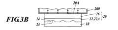
次に、図3〜図5を参照しながらウェハレンズ1の製造方法について説明する。
図3Aに示す通り、マスター10上に樹脂材料22Aをディスペンスする。このとき真空引きしながら樹脂材料22Aをディスペンスしてもよい。真空引きしながら樹脂材料22Aをディスペンスすれば、樹脂材料22Aに気泡を混入させずに樹脂材料22Aを硬化させることができる。Next, a method for manufacturing the
As shown in FIG. 3A, the resin material 22 </ b> A is dispensed on the
そして、樹脂材料22Aを光照射により硬化させ、マスター10の凸部14を樹脂材料22Aに転写し、樹脂材料22Aに対し複数の凹部24を形成する。これにより、サブマスター成形部22が形成される。
光照射に使用する光源50としては、高圧水銀ランプ、メタルハライドランプ、キセノンランプ、ハロゲンランプ、蛍光灯、ブラックライト、Gランプ、Fランプ等が挙げられ、線状光源であってもよいし、点状光源であってもよい。高圧水銀ランプは、365nm、436nmに狭いスペクトルを持つランプである。メタルハライドランプは、水銀灯の一種で、紫外域における出力は高圧水銀ランプよりも数倍高い。キセノンランプは、最も太陽光に近いスペクトルを持つランプである。ハロゲンランプは長波長の光を多く含んでおり、近赤外光がほとんどであるランプである。蛍光灯は光の三原色に均等な照射強度を持っている。ブラックライトはピークトップを351nmに持ち、300nm〜400nmの近紫外光を放射するライトである。
光源50から光照射する場合には、複数の線状又は点状の光源50を格子状に配置して樹脂材料22Aの全面に一度に光が到達するようにしてもよいし、線状又は点状の光源50を樹脂材料22Aの表面に対し平行にスキャニングして樹脂材料22Aに順次光が到達するようにしてもよい。この場合、好ましくは光照射時の輝度分布や照度(強度)分布を測定し、その測定結果に基づき照射回数,照射量,照射時間等を制御する。
樹脂材料22Aを光硬化させた後(サブマスター20の作製後)においては、サブマスター20に対しポストキュア(加熱処理)をおこなってもよい。ポストキュアをおこなえば、サブマスター20の樹脂材料22Aを完全に硬化させることができ、サブマスター20の型寿命を延ばすことができる。Then, the resin material 22A is cured by light irradiation, the
Examples of the
When irradiating light from the
After the resin material 22A is photocured (after the production of the sub master 20), the
図3Bに示す通り、サブマスター成形部22に対しサブマスター基板26を接着する。サブマスター成形部22とサブマスター基板26との密着性を高めるために、サブマスター基板26に対しシランカップリング剤を塗布するなどの処理を行ってもよい。 As shown in FIG. 3B, the
なお、上記のように、マスター10の凸部14を樹脂材料22Aに転写し、樹脂材料22Aが硬化した後(つまりサブマスター成形部22が形成された後)に、サブマスター基板26を装着する場合には、接着剤を使う。
逆に、マスター10の凸部14を樹脂材料22Aに転写し樹脂22Aが硬化する前に、サブマスター基板26を装着するようにしてもよい。この場合には、接着剤を使用せずに、樹脂材料22Aの付着力によりサブマスター基板26を張り付かせるか、又はサブマスター基板26にカップリング剤を塗布し付着力を強くして樹脂材料22Aに対してサブマスター基板26を付着させる。また、サブマスター基板26で裏打ちしつつ硬化させる方法としては、樹脂材料22AとしてUV硬化性樹脂を用いるとともに、サブマスター基板26としてUV透過性の基板を用い、マスター10とサブマスター基板26との間に当該樹脂材料22Aを充填した状態でサブマスター基板26の側から樹脂材料22Aに対してUV光を照射する方法などがある。As described above, the
Conversely, the
また、サブマスター成形部22(樹脂材料22A)をサブマスター基板26で裏打ちする際には、従来より公知の真空チャック装置260を用い、この真空チャック装置260の吸引面260Aにサブマスター基板26を吸引保持しつつ、当該吸引面260Aをマスター10における凸部14の成形面に対して平行な状態として、サブマスター成形部22をサブマスター基板26で裏打ちすることが好ましい。 Further, when backing the sub master molding portion 22 (resin material 22A) with the
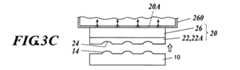
その後、図3Cに示す通り、マスター10からサブマスター成形部22とサブマスター基板26とを離型し、サブマスター20が作製される。
その後、図3Dに示す通り、サブマスター20上に樹脂材料5Aをディスペンスする(ディスペンス工程)。この際に、ディスペンスする樹脂材料5Aの粘度が1000〜10000cPとなるようにディスペンサーを加熱しながらディスペンスする。このとき、使用する樹脂材料5Aは常温(25℃)における粘度が10000cP以上の光硬化性樹脂材料とする。特に、ナノコンポジット樹脂材料をディスペンスする場合には、熱を常時かけて粘度を下げて成形することが好ましい。また、サブマスター20も樹脂材料5Aと実質的に同温度になるように加熱しておくことが好ましい。このように樹脂材料5Aを上記粘度となるように加熱しながらディスペンスすることによって、樹脂材料5Aの糸切れの悪さが改善され、ディスペンス量が安定する。
なお、粘度の測定方法に関しては、振動式粘度計で測定することができる。Thereafter, as shown in FIG. 3C, the sub master molding unit 22 and the
Thereafter, as shown in FIG. 3D, the
In addition, regarding the measuring method of a viscosity, it can measure with a vibratory viscometer.
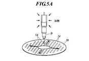
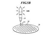
ここで、ディスペンスの方法としては、図5Aに示す通り、サブマスター20の中央に、ディスペンサーDで樹脂材料5Aの全量をディスペンスする中央滴下、すなわち、光硬化性樹脂材料をサブマスター20中央部に配置し、サブマスター20の複数の凹部24にまたがるようにディスペンスするようにしてもよいし、図5Bに示す通り、サブマスター20の各凹部24内に個別に樹脂材料5Aをディスペンスする個別滴下、すなわち、光硬化性樹脂材料をサブマスター20の各凹部24にそれぞれディスペンスするようにしてもよい。
なお、図5中に示すサブマスター20の凹部24の個数及びサブマスター20の形状は、図面の関係上、図2と異なっているが実際は同じものを使用するものとする。
なお、マスター10に樹脂材料22Aをディスペンスする際にも、ディスペンサーを加熱してディスペンスする樹脂材料22Aの粘度が1000〜10000cPとなるように加熱しながらディスペンスしても良い。ディスペンスする樹脂材料22Aは常温(25℃)における粘度が10000cP以上の光硬化性樹脂材料が好ましい。また、マスター10も樹脂22Aの温度と実質的に同温度になるように加熱しておくことが好ましい。Here, as a dispensing method, as shown in FIG. 5A, the central dropping of dispensing the entire amount of the
In addition, although the number of the recessed
In addition, when dispensing the resin material 22A to the
また、真空引きしながら樹脂材料5Aをディスペンスしてもよい。
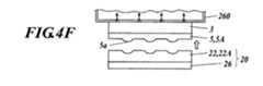
そして、図3Eに示す通り、樹脂材料5Aに対し、その上方からガラス基板3を押圧して樹脂材料5Aを押し広げながら、硬化させる(硬化工程)。また、ガラス基板3で樹脂材料5Aを押圧しながら押し広げる際に、ディスペンス時に加熱した樹脂材料5Aと実質的に同温度になるようにガラス基板3及びサブマスター20を加熱することが好ましい。ガラス基板3及びサブマスター20も樹脂材料5Aと実質的に同温度になるように加熱することによって、樹脂材料5Aを押し広げる際の粘度も10000cP以下に維持することができるため、樹脂材料5Aの押し広げが容易となり、短時間で均一な膜厚で樹脂材料5Aを広げることができる。
なお、本実施形態のように、ウェハレンズの樹脂層が、レンズ部と、その周囲の平坦部とを有するものである場合、成形時における成形型と基板との相対的な押圧力が高くなりがちであるが、上述のように樹脂材料を加熱しておくことで成形を容易にすることができる。なお、上述した実施形態では、ガラス基板3をサブマスター20に向けて押圧しているが、これに代えて、間に樹脂材料を介在させてサブマスター20をガラス基板3に向けて押圧してもよいし、両者ともに互いに接近させるようにしてもよい。要は、サブマスター20とガラス基板3が相対的に接近することで樹脂材料が押圧されればよい。Further, the
Then, as shown in FIG. 3E, the
Note that when the resin layer of the wafer lens has a lens portion and a flat portion around the lens portion as in this embodiment, the relative pressing force between the mold and the substrate during molding becomes high. However, the molding can be facilitated by heating the resin material as described above. In the above-described embodiment, the
樹脂材料5Aを硬化させる場合には、ガラス基板3の上方に配置した光源52によってガラス基板3側から光照射しても良いし、サブマスター20の下方に配置した光源(図示しない)によってサブマスター20側から光照射しても良いし、ガラス基板3側及びサブマスター20側からの両方から光照射しても良い。光源52としては、上述の光源50と同様のものを使用することができる。 When the
図4Fに示す通り、サブマスター20から樹脂部5とガラス基板3とを離型する(離型工程)。このようにしてガラス基板3の一方の面に凸レンズ部5aが形成される。 As shown in FIG. 4F, the resin part 5 and the
続いて、ガラス基板3の他方の面に凹レンズ部6aを形成する方法について説明する。
この場合、凹レンズ部6aに対応するポジ形状の成形面を有するマスター(図示しない)を用意し、このマスターを使用して、凹レンズ部6aに対応するネガ形状の成形面を有するサブマスター20Bを形成する。そして、図4Gに示す通り、凹レンズ部6aに対応するネガ形状の成形面を有するサブマスター20B上に、図3Dと同様にして樹脂材料6Aをディスペンスする。つまり、ディスペンサーを加熱して、ディスペンスする樹脂材料6Aの粘度が1000〜10000cPとなるように加熱しながらディスペンスする。ディスペンスした後、このサブマスター20Bと、図4Fで形成したガラス基板3及び樹脂部5を上下反転させたガラス基板3とを当接させて、ガラス基板3及びサブマスター20Bの間に樹脂材料6Aを充填した状態にする。その後、光照射により樹脂材料6Aを硬化させる。
最後に、サブマスター20Bと、ガラス基板3及び樹脂部6とを離型する。このようにして図4Hに示す通り、ガラス基板3に凸レンズ部5a及び凹レンズ部6aを有するウェハレンズ1が作製される。Then, the method to form the
In this case, a master (not shown) having a positive molding surface corresponding to the
Finally, the
なお、上述の方法では、ガラス基板3の片面ずつに樹脂材料5A、6Aをディスペンスして、硬化させるとしたが、図3Eの状態で樹脂材料5Aを完全に硬化させる前に、上下反転させ、図4Gのサブマスター20B上にディスペンスした樹脂材料6Aに対してガラス基板3を当接させ、サブマスター20の上方及びサブマスター20Bの下方からそれぞれ光照射することで樹脂材料5A,6Aを一括して硬化させてもよい。
また、図4Fでサブマスター20から離型した後、ガラス基板3及び樹脂部5を上下反転させずに、ガラス基板3の他方の面に樹脂材料6Aを塗布し、樹脂6Aの上方からサブマスター20Bを押圧させて、サブマスター20の上方及びサブマスター20Bの下方からそれぞれ光照射することで樹脂材料5A,6Aを一括して硬化させてもよい。In the above-described method, the
4F, after releasing from the
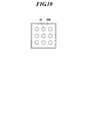
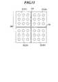
ここで、ガラス基板3の表裏両面に樹脂部5を形成する場合に、図9に示す通りにサブマスター20を縦横2倍ずつ(倍率は変更可能である。)大きくしたような一体型の大径サブマスター200と、図10の通常の大きさのサブマスター20Bとを準備し、ガラス基板3の表面に樹脂部5を形成する場合にはサブマスター200を使用し、その反対側の裏面に樹脂部6を形成する場合にはサブマスター20Bを複数回にわたり使用するようにしてもよい。 Here, when the resin portions 5 are formed on both the front and back surfaces of the
具体的には、ガラス基板3の表面に対しては大径サブマスター200を用いて樹脂部5を一括で形成する。その後のガラス基板3の裏面に対しては、図11に示す通り、サブマスター20Bを大径サブマスター200の1/4区画ずつそれぞれずらしながら4回にわたりサブマスター20Bを用いて樹脂部6を形成する。このような構成によれば、大径サブマスター200を用いて形成した樹脂部5を有するガラス基板3に対し、サブマスター20Bの軸合わせが容易となり、大径サブマスター200を用いて形成した樹脂部5と、サブマスター20Bを用いて形成した樹脂部5とがガラス基板3の表裏において配置がずれるといった事態を抑えることができる。 Specifically, the resin part 5 is collectively formed on the surface of the
ただし、大径サブマスター200を使用する場合には、図12上段から下段に示す通り、そのサブマスター成形部22に対しやや反りが発生する可能性があり、型としての本来の機能を発揮することができない場合もある。そこで、図13に示す通り大径サブマスター200を分割するようにその中央部に十字状に樹脂材料22Aが存在しない領域(応力緩和部210)を設けて、大径サブマスター200のサブマスター成形部22の反りの発生を抑える(ガラス基板3との応力を緩和する)ような構成とするのが好ましい。 However, when the large-
応力緩和部210を設ける場合において、例えば樹脂材料22Aが光硬化性樹脂材料であるときには、ガラス基板3又はサブマスター基板26をマスキングして光の未照射部を形成したり、光源52,54をマスキングして光の未照射部を形成したりすればよい。 In the case where the
なお、上記実施形態では、マスター10からサブマスター20を作製し、サブマスター20から樹脂部5を成形するとしたが、マスター(図示しない)から直接的に樹脂部5を成形してもよい。この場合、使用するマスターは、凸レンズ部5aに対応するネガ形状の凹部を有するものとする。そして、マスターの凹部に対し、図3Dと同様の方法で、樹脂材料5Aをディスペンスし、その上方からガラス基板3を押圧しながら樹脂材料5Aを硬化させ、その後ガラス基板3と樹脂部5とをマスターから離型すればよい。
同様にして、樹脂部6も凹レンズ部6aに対応するネガ形状の凸部を有するマスター(図示しない)から直接的に成形してもよい。In the above embodiment, the
Similarly, the resin part 6 may also be directly molded from a master (not shown) having a negative convex part corresponding to the
《第2の実施形態》
第2の実施形態は主には第1の実施形態と下記の点で異なっており、それ以外は略同じとなっている。<< Second Embodiment >>
The second embodiment is mainly different from the first embodiment in the following points, and is otherwise substantially the same.
ウェハレンズ1の製造にあたって、成形用の型として、図6のマスター10B,サブマスター30,サブサブマスター40が使用される。第1の実施形態では、マスター10からウェハレンズ1を製造するのにサブマスター20を使用したのに対し、第2の実施形態では、主に、マスター10Bからウェハレンズ1を製造するのにサブマスター30,サブサブマスター40の2つの型を使用する点が異なっている。特に、マスター10Bからサブマスター30を作製する工程やサブサブマスター40からウェハレンズ1を製造する工程は第1の実施形態と略同じであり、サブマスター30からサブサブマスター40を作製する点が第1の実施形態と異なっている。 When the
(マスター)
マスター10Bは、直方体状のベース部12に対し複数の凹部16がアレイ状に形成されている。凹部16はウェハレンズ1の凸レンズ部5aに対応するネガ形状となっており、この図では略半球形状に凹んでいる。マスター10Bの外形状は四角形でなくとも良く、円柱状であっても良いが、ここでは四角形状を例として説明する。
なお、マスター10Bの材料等は、上述したマスター10と同様である。(Master)
The
In addition, the material of the
(サブマスター)
サブマスター30は、サブマスター成形部32とサブマスター基板36とで構成されている。サブマスター成形部32には複数の凸部34がアレイ状に形成されている。凸部34の表面(成形面)形状はウェハレンズ1における凸レンズ部5aに対応するポジ形状となっており、この図では略半球形状となっている。(Submaster)
The
サブマスター成形部32は、樹脂材料32Aによって形成されている。樹脂材料32Aは、上記第1の実施形態のサブマスター20と同様の材料を使用することができる。
サブマスター基板36は、サブマスター基板26と同様の材料を使用することができる。The sub
The
(サブサブマスター)
サブサブマスター40は、サブサブマスター成形部42とサブサブマスター基板46とで構成されている。
サブサブマスター成形部42には複数の凹部44がアレイ状に形成されている。凹部44の表面(成形面)形状はウェハレンズ1における凸レンズ部5aに対応するネガ形状となっており、この図では略半球形状に凹んでいる。
サブサブマスター成形部42は、サブマスター成形部32の樹脂材料32Aと同様の樹脂材料42Aから構成され、サブサブマスター基板46は、サブマスター基板36と同様の材料から構成される。(Sub-submaster)
The
A plurality of
The sub-sub
次に、図7、図8を参照しながら、ウェハレンズ1の製造方法について簡単に説明する。
図7Aに示す通り、マスター10B上に樹脂材料32Aをディスペンスする。そして、樹脂材料32Aを光照射により硬化させ、マスター10Bの凹部16を樹脂材料32Aに転写し、樹脂材料32Aに対し複数の凸部34を形成する。これにより、サブマスター成形部32が形成される。
図7Bに示す通り、サブマスター成形部32に対しサブマスター基板36を接着する。
その後、図7Cに示す通り、マスター10Bからサブマスター成形部32とサブマスター基板36とを離型し、サブマスター30が作製される。Next, a method for manufacturing the
As shown in FIG. 7A, the resin material 32A is dispensed on the
As shown in FIG. 7B, the
Thereafter, as shown in FIG. 7C, the sub
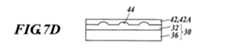
その後、図7Dに示す通り、サブマスター30上に樹脂材料42Aをディスペンスする。そして、樹脂材料42Aを光照射により硬化させ、サブマスター30の凸部34を樹脂42Aに転写し、樹脂材料42Aに対し複数の凹部44を形成する。これにより、サブサブマスター成形部42が形成される。
その後、図7Eに示す通り、サブサブマスター成形部42に対しサブサブマスター基板46を装着する。Thereafter, as shown in FIG. 7D, the
Thereafter, as shown in FIG. 7E, the
図8Fに示す通り、サブマスター30からサブサブマスター成形部42とサブサブマスター基板46とを離型し、サブサブマスター40が作製される。 As shown in FIG. 8F, the sub-sub
図8Gに示す通り、サブサブマスター40上に樹脂材料5Aをディスペンスする(ディスペンス工程)。この際に、ディスペンスする樹脂材料5Aの粘度が1000〜10000cPとなるようにディスペンサーを加熱しながらディスペンスする。このとき、使用する樹脂材料5Aは常温(25℃)における粘度が10000cP以上の光硬化性樹脂材料とする。また、サブサブマスター40も樹脂材料5Aの温度と実質的に同温度となるように加熱しておくことが好ましい。ディスペンスの方法としては、上記中央滴下(図5A参照)又は個別滴下(図5B参照)いずれでもよい。
なお、マスター10Bに樹脂材料22Aを、サブマスター30に樹脂材料42Aを、それぞれディスペンスする際にも、ディスペンサーを加熱してディスペンスする樹脂材料22A,42Aの粘度が1000〜10000cPとなるように加熱しながらディスペンスしても良い。ディスペンスする樹脂材料22A,42Aは常温(25℃)における粘度が10000cP以上の光硬化性樹脂材料が好ましい。また、マスター10やサブマスター30も樹脂材料22A,42Aの温度と実質的に同温度になるように加熱しておくことが好ましい。As shown in FIG. 8G, the
In addition, when dispensing the resin material 22A to the
その後、上方からガラス基板3を押圧して樹脂材料5Aを押し広げながら、硬化させる(硬化工程)。また、ガラス基板3で樹脂材料5Aを押圧しながら押し広げる際に、ディスペンス時に加熱した樹脂材料5Aと同温度になるようにガラス基板3及びサブサブマスター40を加熱することが好ましい。
樹脂材料5Aを硬化させる場合には、図示しない光源によってガラス基板3側から又はサブサブマスター40側からの少なくとも一方から光照射すれば良い。
その結果、樹脂材料5Aから樹脂部5が形成される。その後、樹脂部5とガラス基板3とをサブサブマスター40から離型する(離型工程)。このようにしてガラス基板3の一方の面に凸レンズ部5aが形成される。Thereafter, the
In the case of curing the
As a result, the resin portion 5 is formed from the
続いて、ガラス基板3の他方の面に凹レンズ部6aを形成する方法について説明する。
この場合、凹レンズ部6aに対応するネガ形状の成形面を有するマスター(図示しない)を用意し、マスターを使用して、凹レンズ部6aに対応するポジ形状の成形面を有するサブマスター(図示しない)を形成する。さらに、サブマスターを用いて凹レンズ部6aに対応するネガ形状の成形面を有するサブサブマスター40Bを形成する。
そして、図8Hに示す通り、サブサブマスター40B上に、図8Gと同様にして樹脂材料6Aをディスペンスした後、このサブサブマスター40Bと、図8Gで形成したガラス基板3及び樹脂部5を上下反転させたガラス基板3とを当接させて、ガラス基板3及びサブサブマスター40Bの間に樹脂材料6Aを充填した状態にする。その後、光照射により樹脂材料6Aを硬化させる。
最後に、サブサブマスター40Bと、ガラス基板3及び樹脂部6とを離型する。このようにして図8Iに示す通り、ガラス基板3に凸レンズ部5a及び凹レンズ部6aを有するウェハレンズ1が作製される。
ウェハレンズ1はこの後、レンズ部毎にダイシングされることにより、個片化されたレンズとなる。Then, the method to form the
In this case, a master (not shown) having a negative molding surface corresponding to the
Then, as shown in FIG. 8H, after the resin material 6A is dispensed on the sub-submaster 40B in the same manner as in FIG. 8G, the sub-submaster 40B, the
Finally, the sub-submaster 40B is released from the
After that, the
下記に示す条件及び下記表1に従って、「サンプル1〜サンプル16」のウェハレンズを作製した。なお、ウェハレンズの作製については、上述した第2の実施形態の手順に従って作製するものとする。
基板:8インチガラス基板
サブサブマスター:1000個の凹部を有する8インチの樹脂製
ディスペンスする樹脂材料:常温(25℃)の粘度が15000cPの樹脂材料として、重合開始剤として芳香族スルホニウムを含むビスフェノールA型エポキシ樹脂材料を用いた。また、常温(25℃)の粘度が45000cPの樹脂材料として、重合開始剤として芳香族スルホニウムを含むビスフェノールA型エポキシ樹脂材料にシリカナノ粒子を20wt%添加したものを用いた。
樹脂材料のディスペンス量狙い値:2500mg
ディスペンス方法:中央滴下又は個別滴下According to the conditions shown below and Table 1 below, wafer lenses of “
Substrate: 8-inch glass substrate Sub-submaster: Resin material to be dispensed: 8-inch resin with 1000 recesses: Bisphenol A containing aromatic sulfonium as a polymerization initiator as a resin material having a viscosity of 15000 cP at room temperature (25 ° C.) A type epoxy resin material was used. Moreover, what added 20 wt% of silica nanoparticles to the bisphenol A type epoxy resin material which contains aromatic sulfonium as a polymerization initiator was used as a resin material having a viscosity of 45000 cP at room temperature (25 ° C.).
Target amount of resin material dispensed: 2500mg
Dispensing method: Center dripping or individual dripping
(粘度測定)
振動式粘度計で測定を行った。測定した値を表1に示した。
(樹脂材料の実際のディスペンス量)
樹脂材料のディスペンス量の測定し、ディスペンス量の狙い値に対する差分(mg)をディスペンス量誤差とした。ディスペンス量誤差の値が小さいほど、ディスペンス時の樹脂材料の糸切れがよくディスペンス量が安定していることを示している。特にディスペンス量誤差が10mg未満である場合、ディスペンス量の安定性が多く好ましい。結果を表1に示した。
(心厚測定)
FB心厚測定機(コニカミノルタオプト株式会社製)でウェハレンズの心厚測定を行い、設定値に対する差分(μm)をレンズ心厚誤差とした。レンズ心厚誤差の値が小さいほど、ディスペンス時のディスペンス量が安定していることを示している。特にレンズ心厚誤差が10μm未満であると光学性能が低下しにくく好ましい。結果を表1に示した。
(樹脂材料の押し広げ時間)
成形機を用いて100Nで加圧していき、サブサブマスター上に設けられたレンズ部の光学面形状に対応する1000個の凹部の全てに樹脂材料が充填され、レンズ部の心厚(レンズ頂部から基板までの距離と基板厚みとを加算した厚さ)が設定値である500μmに達するまでの時間を測定し、樹脂材料の押し広げ時間とした。加熱により樹脂材料の粘度が下がると、成形型とガラス基材とに挟まれて樹脂材料が押圧される際の拡散性が増大し、押し広げ時間が短縮される。これによってウェハレンズ製造のためのタクトタイムの短縮に寄与する。(Viscosity measurement)
Measurement was performed with a vibration viscometer. The measured values are shown in Table 1.
(Actual dispensing amount of resin material)
The dispense amount of the resin material was measured, and the difference (mg) with respect to the target value of the dispense amount was defined as the dispense amount error. A smaller value of the dispense amount error indicates that the yarn breakage of the resin material at the time of dispensing is better and the dispense amount is more stable. Particularly, when the dispense amount error is less than 10 mg, the dispense amount is stable and preferable. The results are shown in Table 1.
(Heart thickness measurement)
The wafer lens core thickness was measured with an FB core thickness measuring machine (manufactured by Konica Minolta Opto Co., Ltd.), and the difference (μm) relative to the set value was taken as the lens core thickness error. The smaller the lens thickness error value, the more stable the dispensing amount during dispensing. In particular, it is preferable that the lens core thickness error is less than 10 μm because the optical performance is hardly deteriorated. The results are shown in Table 1.
(Plastic material spreading time)
Using a molding machine, pressurizing with 100 N, resin material is filled in all 1000 concave portions corresponding to the optical surface shape of the lens portion provided on the sub-submaster, and the center thickness of the lens portion (from the top of the lens) The time required for the distance obtained by adding the distance to the substrate and the substrate thickness) to reach the set value of 500 μm was measured and used as the resin material spreading time. When the viscosity of the resin material is lowered by heating, the diffusibility when the resin material is pressed between the mold and the glass substrate is increased, and the spreading time is shortened. This contributes to shortening the tact time for wafer lens manufacture.

表1の結果より、加熱時の粘度が10000cP以下のサンプル5〜8、15,16は、加熱時の粘度が10000cPを越えるサンプル1〜4、9〜14に比べて、ディスペンス量の誤差及びレンズ心厚の誤差が小さいことがわかる。 From the results in Table 1, samples 5 to 8, 15 and 16 having a viscosity at heating of 10000 cP or less are more accurate than the
1 ウェハレンズ
3 ガラス基板
5 樹脂部
5a 凸レンズ部
5b 非レンズ部
5A 樹脂材料
6 樹脂部
6a 凹レンズ部
6b 非レンズ部
6A 樹脂材料
10,10B マスター
12 ベース部
14 凸部
16 凹部
20 サブマスター
22 サブマスター成形部
22A 樹脂材料
24 凹部
25 凸部
26 サブマスター基板
30 サブマスター
32 サブマスター成形部
32A 樹脂材料
34 凸部
36 サブマスター基板
40 サブサブマスター
42 サブサブマスター成形部
42A 樹脂材料
44 凹部
46 サブサブマスター基板
50,52 光源
200 大径サブマスター
210 応力緩和部
D ディスペンサーDESCRIPTION OF
Claims (12)
Translated fromJapanese前記レンズ部の光学面形状に対応した形状の成形面を有する成形型、及び、前記基板の一方の面の少なくとも一方に光硬化性樹脂材料をディスペンスするディスペンス工程と、
前記ディスペンス工程後、前記光硬化性樹脂材料を前記成形型及び前記基板を相対的に接近させることによって押圧し、前記光硬化性樹脂材料に光を照射させて硬化させる硬化工程と、
前記硬化工程後、硬化により形成されたレンズ部を前記成形型から離型する離型工程と、を備え、
前記基板及び前記成形型の両者又はいずれか一方は、光透過性を有する材料で構成され、前記硬化工程は、前記基板の上方又は前記成形型の下方から前記光硬化性樹脂材料に光を照射させる光照射工程を含み、
前記光硬化性樹脂材料は、25℃における粘度が10000cP以上であり、
前記ディスペンス工程では、前記光硬化性樹脂材料が1000cP以上10000cP以下となるように加熱してディスペンスすることを特徴とするウェハレンズの製造方法。A wafer lens manufacturing method in which a lens portion made of a photocurable resin is provided on one surface of a substrate,
A molding die having a molding surface having a shape corresponding to the optical surface shape of the lens portion, and a dispensing step of dispensing a photocurable resin material on at least one of the one surface of the substrate;
After the dispensing step, the photocurable resin material is pressed by bringing the mold and the substrate relatively close to each other, and the photocurable resin material is irradiated with light to be cured, and
A mold release step for releasing the lens part formed by the curing from the mold after the curing step;
Either or both of the substrate and the mold are made of a light-transmitting material, and the curing step irradiates the photocurable resin material with light from above the substrate or from below the mold. Including a light irradiation step
The photocurable resin material has a viscosity at 25 ° C. of 10,000 cP or more,
In the dispensing step, the wafer curable resin material is heated and dispensed so that the photocurable resin material has a viscosity of 1000 cP or more and 10,000 cP or less.
前記成形型は前記複数のレンズ部の光学面形状に対応した複数の成形部を備えた成形面を有していることを特徴とする請求項1〜8のいずれか一項に記載のウェハレンズの製造方法。The wafer lens is provided with a plurality of lens portions made of the photocurable resin on one surface of the substrate,
The wafer lens according to claim 1, wherein the mold has a molding surface having a plurality of molding parts corresponding to the optical surface shape of the plurality of lens parts. Manufacturing method.
Priority Applications (1)
| Application Number | Priority Date | Filing Date | Title |
|---|---|---|---|
| JP2012517205AJP5678958B2 (en) | 2010-05-27 | 2011-04-28 | Wafer lens manufacturing method |
Applications Claiming Priority (4)
| Application Number | Priority Date | Filing Date | Title |
|---|---|---|---|
| JP2010121483 | 2010-05-27 | ||
| JP2010121483 | 2010-05-27 | ||
| PCT/JP2011/060349WO2011148756A1 (en) | 2010-05-27 | 2011-04-28 | Method for producing wafer lens |
| JP2012517205AJP5678958B2 (en) | 2010-05-27 | 2011-04-28 | Wafer lens manufacturing method |
Publications (2)
| Publication Number | Publication Date |
|---|---|
| JPWO2011148756A1 JPWO2011148756A1 (en) | 2013-07-25 |
| JP5678958B2true JP5678958B2 (en) | 2015-03-04 |
Family
ID=45003748
Family Applications (1)
| Application Number | Title | Priority Date | Filing Date |
|---|---|---|---|
| JP2012517205AExpired - Fee RelatedJP5678958B2 (en) | 2010-05-27 | 2011-04-28 | Wafer lens manufacturing method |
Country Status (3)
| Country | Link |
|---|---|
| US (1) | US20130062800A1 (en) |
| JP (1) | JP5678958B2 (en) |
| WO (1) | WO2011148756A1 (en) |
Families Citing this family (9)
| Publication number | Priority date | Publication date | Assignee | Title |
|---|---|---|---|---|
| JP5009209B2 (en)* | 2008-03-21 | 2012-08-22 | シャープ株式会社 | Wafer-like optical device and manufacturing method thereof, electronic element wafer module, sensor wafer module, electronic element module, sensor module, and electronic information device |
| JP5648501B2 (en)* | 2011-01-28 | 2015-01-07 | コニカミノルタ株式会社 | Manufacturing method of resin molding |
| JP7666878B2 (en)* | 2020-11-18 | 2025-04-22 | 株式会社ディスコ | Wafer manufacturing method and stacked device chip manufacturing method |
| JP7612290B2 (en) | 2020-11-18 | 2025-01-14 | 株式会社ディスコ | Wafer manufacturing method and stacked device chip manufacturing method |
| JP7608019B2 (en) | 2020-11-18 | 2025-01-06 | 株式会社ディスコ | Wafer manufacturing method and stacked device chip manufacturing method |
| JP7608018B2 (en) | 2020-11-18 | 2025-01-06 | 株式会社ディスコ | Wafer manufacturing method and stacked device chip manufacturing method |
| JP7612289B2 (en) | 2020-11-18 | 2025-01-14 | 株式会社ディスコ | Wafer manufacturing method and stacked device chip manufacturing method |
| JP7693298B2 (en)* | 2020-11-18 | 2025-06-17 | 株式会社ディスコ | Wafer manufacturing method and stacked device chip manufacturing method |
| JP7704544B2 (en) | 2021-03-09 | 2025-07-08 | 株式会社ディスコ | Wafer manufacturing method and stacked device chip manufacturing method |
Citations (5)
| Publication number | Priority date | Publication date | Assignee | Title |
|---|---|---|---|---|
| JPH06201903A (en)* | 1992-08-20 | 1994-07-22 | Mitsubishi Rayon Co Ltd | Manufacture of lens sheet |
| JP2006030633A (en)* | 2004-07-16 | 2006-02-02 | Seiko Epson Corp | Microlens manufacturing method and microlens manufacturing apparatus |
| JP2008046469A (en)* | 2006-08-18 | 2008-02-28 | Nikon Corp | Method for manufacturing diffractive optical element and resin discharging apparatus |
| JP2008229861A (en)* | 2007-03-16 | 2008-10-02 | Seiko Epson Corp | Plastic lens manufacturing method and molding mold sealing device |
| JP2010105357A (en)* | 2008-10-31 | 2010-05-13 | Konica Minolta Opto Inc | Molding device, molding die member, wafer lens, and method of manufacturing wafer lens molding die |
Family Cites Families (5)
| Publication number | Priority date | Publication date | Assignee | Title |
|---|---|---|---|---|
| US5801884A (en)* | 1995-10-09 | 1998-09-01 | Mitsubishi Chemical Corporation | Optical device and process for producing the same |
| JPH11326603A (en)* | 1998-05-19 | 1999-11-26 | Seiko Epson Corp | Microlens array, method of manufacturing the same, and display device |
| US6385997B1 (en)* | 2000-05-12 | 2002-05-14 | Eastman Kodak Company | Method for forming a tool for molding microlens arrays |
| JP2006154757A (en)* | 2004-10-26 | 2006-06-15 | Seiko Epson Corp | Microlens substrate manufacturing method, microlens substrate, transmissive screen, and rear projector |
| WO2009120346A1 (en)* | 2008-03-27 | 2009-10-01 | Tessera North America, Inc. | Optical device including at least one replicated surface and associated methods |
- 2011
- 2011-04-28USUS13/700,423patent/US20130062800A1/ennot_activeAbandoned
- 2011-04-28WOPCT/JP2011/060349patent/WO2011148756A1/enactiveApplication Filing
- 2011-04-28JPJP2012517205Apatent/JP5678958B2/ennot_activeExpired - Fee Related
Patent Citations (5)
| Publication number | Priority date | Publication date | Assignee | Title |
|---|---|---|---|---|
| JPH06201903A (en)* | 1992-08-20 | 1994-07-22 | Mitsubishi Rayon Co Ltd | Manufacture of lens sheet |
| JP2006030633A (en)* | 2004-07-16 | 2006-02-02 | Seiko Epson Corp | Microlens manufacturing method and microlens manufacturing apparatus |
| JP2008046469A (en)* | 2006-08-18 | 2008-02-28 | Nikon Corp | Method for manufacturing diffractive optical element and resin discharging apparatus |
| JP2008229861A (en)* | 2007-03-16 | 2008-10-02 | Seiko Epson Corp | Plastic lens manufacturing method and molding mold sealing device |
| JP2010105357A (en)* | 2008-10-31 | 2010-05-13 | Konica Minolta Opto Inc | Molding device, molding die member, wafer lens, and method of manufacturing wafer lens molding die |
Also Published As
| Publication number | Publication date |
|---|---|
| JPWO2011148756A1 (en) | 2013-07-25 |
| US20130062800A1 (en) | 2013-03-14 |
| WO2011148756A1 (en) | 2011-12-01 |
Similar Documents
| Publication | Publication Date | Title |
|---|---|---|
| JP5678958B2 (en) | Wafer lens manufacturing method | |
| JP5617636B2 (en) | Wafer lens manufacturing method | |
| CN103168050B (en) | Semi-cured product, cured product and method for producing the same, optical part, curable resin composition | |
| JP5429159B2 (en) | Wafer lens manufacturing method | |
| JP2013001091A (en) | Method of manufacturing optical element | |
| TW200918975A (en) | Light guide with flexibility and durability | |
| JP7549091B2 (en) | Light source unit, optical unit, and method for manufacturing the light source unit | |
| JPWO2009116371A1 (en) | Wafer lens manufacturing method | |
| JP2010169708A (en) | Composite optical element | |
| JP5327221B2 (en) | Method for manufacturing wafer lens or wafer lens assembly | |
| JP2010107891A (en) | Wafer lens assemblage and method of manufacturing the same, lens unit, and imaging device | |
| JP2013125059A (en) | Lens unit and method of manufacturing the same, and lens unit complex and method of manufacturing the same | |
| JP5685054B2 (en) | Semi-cured product, cured product and production method thereof, optical component, cured resin composition | |
| JP2009226638A (en) | Method for manufacturing wafer lens | |
| JP2010105357A (en) | Molding device, molding die member, wafer lens, and method of manufacturing wafer lens molding die | |
| WO2010119726A1 (en) | Method for manufacturing wafer lens | |
| JP2010211115A (en) | Composite optical element | |
| JP2009226637A (en) | Method for manufacturing master molding die | |
| JP2004346125A (en) | Optical curing type resin composition and light-resistant optical part | |
| JP2009226631A (en) | Manufacturing method of wafer lens | |
| WO2012160769A1 (en) | Method for manufacturing resin molded article | |
| WO2012060342A1 (en) | Method for producing wafer lens | |
| JP5130977B2 (en) | Sub master mold manufacturing method | |
| JP2012052016A (en) | Material composition and optical element using the same | |
| JP2013122480A (en) | Wafer lens and method for manufacturing the same |
Legal Events
| Date | Code | Title | Description |
|---|---|---|---|
| A131 | Notification of reasons for refusal | Free format text:JAPANESE INTERMEDIATE CODE: A131 Effective date:20140916 | |
| A521 | Request for written amendment filed | Free format text:JAPANESE INTERMEDIATE CODE: A523 Effective date:20141106 | |
| TRDD | Decision of grant or rejection written | ||
| A01 | Written decision to grant a patent or to grant a registration (utility model) | Free format text:JAPANESE INTERMEDIATE CODE: A01 Effective date:20141209 | |
| A61 | First payment of annual fees (during grant procedure) | Free format text:JAPANESE INTERMEDIATE CODE: A61 Effective date:20141222 | |
| R150 | Certificate of patent or registration of utility model | Ref document number:5678958 Country of ref document:JP Free format text:JAPANESE INTERMEDIATE CODE: R150 | |
| LAPS | Cancellation because of no payment of annual fees |