JP5678485B2 - Semiconductor device - Google Patents
Semiconductor deviceDownload PDFInfo
- Publication number
- JP5678485B2 JP5678485B2JP2010134698AJP2010134698AJP5678485B2JP 5678485 B2JP5678485 B2JP 5678485B2JP 2010134698 AJP2010134698 AJP 2010134698AJP 2010134698 AJP2010134698 AJP 2010134698AJP 5678485 B2JP5678485 B2JP 5678485B2
- Authority
- JP
- Japan
- Prior art keywords
- layer
- type
- region
- gate
- channel
- Prior art date
- Legal status (The legal status is an assumption and is not a legal conclusion. Google has not performed a legal analysis and makes no representation as to the accuracy of the status listed.)
- Expired - Fee Related
Links
Images


Classifications
- H—ELECTRICITY
- H10—SEMICONDUCTOR DEVICES; ELECTRIC SOLID-STATE DEVICES NOT OTHERWISE PROVIDED FOR
- H10D—INORGANIC ELECTRIC SEMICONDUCTOR DEVICES
- H10D30/00—Field-effect transistors [FET]
- H10D30/40—FETs having zero-dimensional [0D], one-dimensional [1D] or two-dimensional [2D] charge carrier gas channels
- H10D30/47—FETs having zero-dimensional [0D], one-dimensional [1D] or two-dimensional [2D] charge carrier gas channels having 2D charge carrier gas channels, e.g. nanoribbon FETs or high electron mobility transistors [HEMT]
- H10D30/471—High electron mobility transistors [HEMT] or high hole mobility transistors [HHMT]
- H10D30/475—High electron mobility transistors [HEMT] or high hole mobility transistors [HHMT] having wider bandgap layer formed on top of lower bandgap active layer, e.g. undoped barrier HEMTs such as i-AlGaN/GaN HEMTs
- H10D30/4755—High electron mobility transistors [HEMT] or high hole mobility transistors [HHMT] having wider bandgap layer formed on top of lower bandgap active layer, e.g. undoped barrier HEMTs such as i-AlGaN/GaN HEMTs having wide bandgap charge-carrier supplying layers, e.g. modulation doped HEMTs such as n-AlGaAs/GaAs HEMTs
- H—ELECTRICITY
- H10—SEMICONDUCTOR DEVICES; ELECTRIC SOLID-STATE DEVICES NOT OTHERWISE PROVIDED FOR
- H10D—INORGANIC ELECTRIC SEMICONDUCTOR DEVICES
- H10D30/00—Field-effect transistors [FET]
- H10D30/01—Manufacture or treatment
- H10D30/015—Manufacture or treatment of FETs having heterojunction interface channels or heterojunction gate electrodes, e.g. HEMT
- H—ELECTRICITY
- H10—SEMICONDUCTOR DEVICES; ELECTRIC SOLID-STATE DEVICES NOT OTHERWISE PROVIDED FOR
- H10D—INORGANIC ELECTRIC SEMICONDUCTOR DEVICES
- H10D62/00—Semiconductor bodies, or regions thereof, of devices having potential barriers
- H10D62/80—Semiconductor bodies, or regions thereof, of devices having potential barriers characterised by the materials
- H10D62/82—Heterojunctions
- H10D62/824—Heterojunctions comprising only Group III-V materials heterojunctions, e.g. GaN/AlGaN heterojunctions
- H—ELECTRICITY
- H10—SEMICONDUCTOR DEVICES; ELECTRIC SOLID-STATE DEVICES NOT OTHERWISE PROVIDED FOR
- H10D—INORGANIC ELECTRIC SEMICONDUCTOR DEVICES
- H10D84/00—Integrated devices formed in or on semiconductor substrates that comprise only semiconducting layers, e.g. on Si wafers or on GaAs-on-Si wafers
- H10D84/01—Manufacture or treatment
- H10D84/0123—Integrating together multiple components covered by H10D12/00 or H10D30/00, e.g. integrating multiple IGBTs
- H—ELECTRICITY
- H10—SEMICONDUCTOR DEVICES; ELECTRIC SOLID-STATE DEVICES NOT OTHERWISE PROVIDED FOR
- H10D—INORGANIC ELECTRIC SEMICONDUCTOR DEVICES
- H10D84/00—Integrated devices formed in or on semiconductor substrates that comprise only semiconducting layers, e.g. on Si wafers or on GaAs-on-Si wafers
- H10D84/80—Integrated devices formed in or on semiconductor substrates that comprise only semiconducting layers, e.g. on Si wafers or on GaAs-on-Si wafers characterised by the integration of at least one component covered by groups H10D12/00 or H10D30/00, e.g. integration of IGFETs
- H10D84/87—Integrated devices formed in or on semiconductor substrates that comprise only semiconducting layers, e.g. on Si wafers or on GaAs-on-Si wafers characterised by the integration of at least one component covered by groups H10D12/00 or H10D30/00, e.g. integration of IGFETs of PN-junction gate FETs
- H—ELECTRICITY
- H01—ELECTRIC ELEMENTS
- H01L—SEMICONDUCTOR DEVICES NOT COVERED BY CLASS H10
- H01L2924/00—Indexing scheme for arrangements or methods for connecting or disconnecting semiconductor or solid-state bodies as covered by H01L24/00
- H01L2924/10—Details of semiconductor or other solid state devices to be connected
- H01L2924/11—Device type
- H01L2924/13—Discrete devices, e.g. 3 terminal devices
- H01L2924/1304—Transistor
- H01L2924/1306—Field-effect transistor [FET]
- H01L2924/13064—High Electron Mobility Transistor [HEMT, HFET [heterostructure FET], MODFET]
- H—ELECTRICITY
- H10—SEMICONDUCTOR DEVICES; ELECTRIC SOLID-STATE DEVICES NOT OTHERWISE PROVIDED FOR
- H10D—INORGANIC ELECTRIC SEMICONDUCTOR DEVICES
- H10D84/00—Integrated devices formed in or on semiconductor substrates that comprise only semiconducting layers, e.g. on Si wafers or on GaAs-on-Si wafers
- H10D84/01—Manufacture or treatment
- H10D84/02—Manufacture or treatment characterised by using material-based technologies
- H10D84/05—Manufacture or treatment characterised by using material-based technologies using Group III-V technology
Landscapes
- Junction Field-Effect Transistors (AREA)
- Electrodes Of Semiconductors (AREA)
Description
Translated fromJapanese本発明は、化合物半導体系の電界効果トランジスタに関し、特にn型の高電子移動度トランジスタとp型の電界効果トランジスタとを同一の化合物半導体基板上に形成した半導体装置に関する。 The present invention relates to a compound semiconductor field effect transistor, and more particularly to a semiconductor device in which an n-type high electron mobility transistor and a p-type field effect transistor are formed on the same compound semiconductor substrate.
GaAs系などの化合物半導体層を持つ電界効果トランジスタは電子移動度が高く、良好な周波数特性を有することから、nチャネルを使って携帯電話などの高周波領域の分野で広く用いられている。現在、高周波数帯に用いられるnチャネルFET(Field Effect Transistor)は、高電子移動度トランジスタ(HEMT:High Electron Mobility
Transistor)が用いられている。また、その変形例であり、エピタキシャル成長によるある程度の格子不整合を許容してさらに高い電子移動度を実現する擬似格子接合高電子移動度トランジスタ(PHEMT:Pseudomorphic HEMT)が知られている。また、ゲート部にPN接合を形成したJPHEMT(Junction Pseudomorphic HEMT)(例えば特許文献1を参照)が知られている。JPHEMTは、ゲートに大きな正電圧を印加してチャネル層に形成されるキャリア欠乏領域を縮小し、チャネル層の寄生抵抗成分を減少させている。A field effect transistor having a compound semiconductor layer such as a GaAs type has high electron mobility and good frequency characteristics, and therefore is widely used in the field of a high frequency region such as a cellular phone using an n channel. Currently, n-channel field effect transistors (FETs) used in high frequency bands are high electron mobility transistors (HEMT).
Transistor) is used. A pseudo-junction high electron mobility transistor (PHEMT: Pseudomorphic HEMT) is also known as a modification thereof, which allows a certain degree of lattice mismatch due to epitaxial growth and realizes higher electron mobility. Further, JPHEMT (Junction Pseudomorphic HEMT) (for example, see Patent Document 1) in which a PN junction is formed in a gate portion is known. JPHEMT applies a large positive voltage to the gate to reduce the carrier-deficient region formed in the channel layer, thereby reducing the parasitic resistance component of the channel layer.
このように、nチャネルFETの高性能化が進んでおり、それに加えて、今後は高集積化が求められており、化合物半導体を用いた相補型(コンプリメンタリ)素子の開発が必要となっている。一般的に、化合物半導体上にnチャネルとpチャネルのFETを同時に形成する方法として、イオン注入技術を使用する手法が知られている。同一基板上にp型ドーパントとn型ドーパントを打ち分けて、nチャネル形成領域とpチャネル形成領域とを形成する。しかし、このイオン技術注入法を利用する場合は、注入したドーパントを活性化させるために、イオン注入後に少なくとも800℃以上の高温アニールを行う必要がある。 As described above, the performance of n-channel FETs is increasing, and in addition to this, high integration is required in the future, and it is necessary to develop complementary devices using compound semiconductors. . In general, as a method for simultaneously forming n-channel and p-channel FETs on a compound semiconductor, a method using an ion implantation technique is known. An n-channel formation region and a p-channel formation region are formed by dividing a p-type dopant and an n-type dopant on the same substrate. However, when this ion technology implantation method is used, it is necessary to perform high-temperature annealing at least 800 ° C. or higher after ion implantation in order to activate the implanted dopant.
特許文献2には、化合物半導体上にnチャネルFETとpチャネルFETを同時に形成する方法が記載されている。GaAsからなる化合物半導体基板上に、2次元電子ガスをキャリアとするnチャネル型ヘテロ接合電界効果トランジスタと、2次元正孔ガスをキャリアとするpチャネル型ヘテロ接合電界効果トランジスタを形成することが記載されている。nチャネル型ヘテロ接合電界効果トランジスタは、ノンドープGaAs層、ノンドープAlGaAs層、n型不純物ドープAlGaAs層、n型不純物ドープGaAs層を備えている。各層はエピタキシャル成長法により積層形成されている。n型不純物ドープAlGaAs層にはアルミニウム又はチタン/白金/金を用いたゲート電極が、n型不純物ドープGaAs層には金ゲルマニウム/金を用いたソース・ドレイン電極がそれぞれ形成されている。pチャネル型ヘテロ接合電界効果トランジスタは、上記積層構造の上にノンドープGaAs層、ノンドープAlGaAs層、p型不純物ドープAlGaAs層、p型不純物ドープGaAs層の各層がエピタキシャル成長法により積層形成されている。p型不純物ドープのAlGaAs層にはAl又はチタン/白金/金を用いたゲート電極が、p型不純物ドープのGaAs層の上には金/亜鉛/金を用いたソース・ドレイン電極がそれぞれ形成されている。
イオン注入技術をHEMTに用いようとすると、不純物のドーピング後に800℃以上の温度で熱処理が必要となる。しかし、ヘテロ接合は温度600℃程度のエピタキシャル成長法により形成されることから、800℃以上のアニール温度ではヘテロ接合界面において化合物組成元素や不純物元素の相互拡散が生じて、意図するヘテロ接合を実現することが困難であった。 If an ion implantation technique is to be used for HEMT, heat treatment is required at a temperature of 800 ° C. or higher after impurity doping. However, since the heterojunction is formed by an epitaxial growth method at a temperature of about 600 ° C., an annealing temperature of 800 ° C. or higher causes mutual diffusion of compound composition elements and impurity elements at the heterojunction interface, thereby realizing the intended heterojunction. It was difficult.
また、特許文献2に記載の各電界効果トランジスタは、各ゲートがショットキー接合型である。このため、閾値電圧を制御すること、あるいはpチャネルの電界効果トランジスタをエンハンスメントモードで動作させることが難しい。そのため、nチャネル電界効果トランジスタとpチャネル電界効果トランジスタを同一基板に形成してリーク電流の小さい相補型トランジスタを構成することが難しい、という課題があった。 In each field effect transistor described in
本発明においては上記課題を解決するために以下の手段を講じた。 In the present invention, the following means have been taken in order to solve the above problems.
請求項1の発明においては、化合物半導体基板と、前記化合物半導体基板の上に形成され、第1チャネル層と、前記第1チャネル層にヘテロ接合し、前記第1チャネル層にn型の電荷を供給するn型の第1障壁層と、前記n型の第1障壁層に対してpn接合型の電位障壁を有するp型のゲート領域とを備えるnチャネル電界効果トランジスタ領域と、前記n型の第1障壁層の上に形成され、p型の第2チャネル層と、ゲートリーク防止層と、前記p型の第2チャネル層に対してpn接合型の電位障壁を有するn型のゲート領域とを含むpチャネル電界効果トランジスタ領域と、から構成され、前記p型の第2チャネル層には、Znの拡散層からなるp型のソース領域とドレイン領域が、前記n型のゲート領域を挟むように互いに離間して形成され、前記第1チャネル層は、不純物が添加されていないi−InGaAs層であり、前記n型の第1障壁層は、前記第1チャネル層の側から順に、前記第1チャネル層との間に良好なヘテロ接合界面を得るために設けられた不純物が添加されていない第1高抵抗層としてのi−AlGaAs層、前記第1チャネル層に電子を供給するために設けられたn型不純物を添加されたn型電荷供給層としてのn+AlGaAs層、n型不純物を添加された第2高抵抗層としてのn−AlGaAs層、の順で積層して形成され、前記p型のゲート領域は、前記第2高抵抗層にZnを拡散したp型領域で形成され、前記p型の第2チャネル層は、前記n型の第1障壁層の上に形成されたn型不純物を含むキャップ層としてのn+GaAs層とその上に形成されたバッファ層としての不純物が添加されていないi−GaAs層との上に形成された、p型不純物を添加されたp−GaAs層で構成され、前記ゲートリーク防止層は、前記p型の第2チャネル層と前記n型のゲート領域との間に、不純物が添加されていないi−AlGaAs層により形成され、前記n型のゲート領域は、n型不純物を添加したn−InGaPから構成されたn型第1ゲート層と、n型不純物を添加したn−GaAsを前記n型第1ゲート層の上に積層して構成されたn型第2ゲート層との2層構造を備え、前記p型のソース領域とドレイン領域は、前記ゲートリーク防止層を貫通し、前記第2チャネル層の一部領域まで延在するように、Znを拡散させた拡散領域により構成されている半導体装置とした。According to a first aspect of the present invention, a compound semiconductor substrate is formed on the compound semiconductor substrate, heterojunctioned with the first channel layer and the first channel layer, and n-type charge is applied to the first channel layer. An n-channel field effect transistor region comprising: ann-type first barrier layer to be supplied; and a p-type gate region having a pn junction-type potential barrier with respect to the n-type first barrier layer; A p-type second channel layer; agate leak prevention layer; and an n-type gate region having a pn junction-type potential barrier with respect to the p-type second channel layer. And ap-type second channel layer including a p-type source region and a drain region made of a Zn diffusion layer sandwiching the n-type gate region. Formed apart from each other The first channel layer is an i-InGaAs layer to which no impurity is added, and the n-type first barrier layer is disposed between the first channel layer and the first channel layer in order from the first channel layer side. An i-AlGaAs layer as a first high-resistance layer to which an impurity is provided to obtain a favorable heterojunction interface and an n-type impurity provided to supply electrons to the first channel layer are provided. An n+AlGaAslayer as an added n-type charge supply layer andan n−AlGaAs layeras a second high-resistance layer to which an n-type impurity is addedare stacked in this order, and the p-type gate region is The p-type region in which Zn is diffused in the second high resistance layer, and the p-type second channel layer is a cap layer including an n-type impurity formed on the n-type first barrier layer.n+ GaAs layerasthe thereon Impurities as it formed the buffer layer is formed on the i-GaAs layer which is not added, p being added p-type impurity-consists of GaAs layer, the gate leak prevention layer, the p-type An i-AlGaAs layer to which no impurity is added is formed between the second channel layer and the n-type gate region, and the n-type gate region is made of n-InGaP towhich an n-type impurity is added.is a n-type first gate layer, n-type impurity was added n-comprises a two-layer structure of a n-type second gate layer formed by laminating a GaAs on the n-type first gate layer, The p-type source region and drain region are constituted by a diffusion region in which Zn is diffused so as to penetrate the gate leak prevention layer and extend to a partial region of the second channel layer. It was.
請求項2の発明においては、前記化合物半導体基板と前記第1チャネル層との間に、前記第1チャネル層にn型の電荷を供給するn型の第2障壁層が形成されており、前記n型の第2障壁層は、前記化合物半導体基板の側から順に、前記第1チャネル層に電子を供給するために設けられたn型不純物を添加されたn型電荷供給層としてのn+AlGaAs層、前記第1チャネル層との間に良好なヘテロ接合界面を得るために設けられた不純物が添加されていない第3高抵抗層としてのi−AlGaAs層、の順で積層して形成されていることを特徴とする請求項1に記載の半導体装置とした。According to a second aspect of the present invention, ann-type second barrier layer that supplies an n-type charge to the first channel layer is formed between the compound semiconductor substrate and the first channel layer. The n-type second barrier layer is an n+AlGaAsas an n-type charge supply layer doped with an n-type impurity provided to supply electrons to the first channel layer in order from the compound semiconductor substrate side.And an i-AlGaAs layer as a third high-resistance layer not added with an impurity provided to obtain a good heterojunction interface between the first channel layer and the first channel layer. It was a semiconductor device according to
請求項3の発明においては、前記pチャネル電界効果トランジスタ領域には、前記n型の第1障壁層上にバックゲート電極が形成されていることを特徴とする請求項1又は請求項2に記載の半導体装置とした。According to a third aspect of the present invention, in thep-channel field effect transistor region, a back gate electrode is formed on the n-type first barrier layer. The semiconductor device was made.
請求項4の発明においては、化合物半導体基板と、前記化合物半導体基板上に形成され、p型の第2チャネル層と、ゲートリーク防止層と、前記p型の第2チャネル層に対してpn接合型の電位障壁を有するn型のゲート領域とを含むpチャネル電界効果トランジスタ領域と、前記p型の第2チャネル層の上に形成され、第1チャネル層と、前記第1チャネル層にヘテロ接合し、前記第1チャネル層にn型の電荷を供給するn型の第1障壁層と、前記n型の第1障壁層に対してpn接合型の電位障壁を有するp型のゲート領域とを備えるnチャネル電界効果トランジスタ領域と、から構成され、前記p型の第2チャネル層には、Znの拡散層からなるp型のソース領域とドレイン領域が、前記n型のゲート領域を挟むように互いに離間して形成され、前記p型の第2チャネル層は、p型不純物を添加されたp−GaAs層で構成され、前記ゲートリーク防止層は、前記p型の第2チャネル層と前記n型のゲート領域との間に、不純物が添加されていないi−AlGaAs層により形成され、前記n型のゲート領域は、n型不純物を添加したn−InGaPから構成されたn型第1ゲート層と、n型不純物を添加したn−GaAsを前記n型第1ゲート層の上に積層して構成されたn型第2ゲート層との2層構造の一部で構成され、前記p型のソース領域とドレイン領域は、前記ゲートリーク防止層を貫通し、前記第2チャネル層の一部領域まで延在するように、Znを拡散させた拡散領域により構成されており、前記第1チャネル層は、前記n型第2ゲート層の上に形成された不純物が添加されていないi−InGaAs層であり、前記n型の第1障壁層は、前記第1チャネル層の側から順に、前記第1チャネル層との間に良好なヘテロ接合界面を得るために設けられた不純物が添加されていない第1高抵抗層としてのi−AlGaAs層、前記第1チャネル層に電子を供給するために設けられたn型不純物を添加されたn型電荷供給層としてのn+AlGaAs層、n型不純物を添加された第2高抵抗層としてのn−AlGaAs層、の順で積層して形成され、前記p型のゲート領域は、前記第2高抵抗層にZnを拡散したp型領域で形成されている半導体装置とした。According to a fourth aspect of the present invention, acompound semiconductor substrate, a p-type second channel layer, a gate leak prevention layer, and a pn junction formed on the p-type second channel layer are formed on the compound semiconductor substrate. A p-channel field effect transistor region including an n-type gate region having a potential barrier of a type, a p-type second channel layer, a first channel layer, and a heterojunction to the first channel layer And an n-type first barrier layer for supplying n-type charge to the first channel layer, and a p-type gate region having a pn junction type potential barrier with respect to the n-type first barrier layer. An n-channel field effect transistor region, and the p-type second channel layer includes a p-type source region and a drain region made of a Zn diffusion layer sandwiching the n-type gate region. Shaped apart from each other Is, the p-type second channel layer of the p was added p-type impurity-consists of GaAs layer, the gate leakage preventing layer, and the p-type second channel layer of said n-type gate region The n-type gate region isformed with an n-type first gate layer made ofn-InGaP doped with an n-type impurity, and an n-type impurity. N-GaAsdoped withn-type GaAs and laminated on the n-type first gate layer, the p-type source region and drain region. Is constituted by a diffusion region in which Zn is diffused so as to penetrate the gate leak prevention layer and extend to a partial region of the second channel layer, and the first channel layer includes the n-type Formed on the second gate layer It is an i-InGaAs layer to which a pure substance is not added, and the n-type first barrier layer obtains a favorable heterojunction interface with the first channel layer in order from the first channel layer side. An i-AlGaAs layer as a first high-resistance layer to which no impurity is added, and an n-type charge supply layer to which an n-type impurity is added to supply electrons to the first channel layern+ AlGaAs layerservingas,nas the second high-resistance layer which is doped with an n-type impurity- AlGaAs layer, is formed by the laminated in this order, a gate region of the p-type, the second high-resistance layer The semiconductor deviceis formed of a p-type region in which Zn is diffused .
請求項5の発明においては、前記n型第2ゲート層と前記第1チャネル層との間に、前記第1チャネル層にn型の電荷を供給するn型の第2障壁層が形成されており、前記n型の第2障壁層は、前記n型第2ゲート層の側から順に、前記第1チャネル層に電子を供給するために設けられたn型不純物を添加されたn型電荷供給層としてのn+AlGaAs層、前記第1チャネル層との間に良好なヘテロ接合界面を得るために設けられた不純物が添加されていない第3高抵抗層としてのi−AlGaAs層、の順で積層して形成されていることを特徴とする請求項4に記載の半導体装置とした。According to a fifth aspect of the present invention, ann-type second barrier layer for supplying an n-type charge to the first channel layer is formed between the n-type second gate layer and the first channel layer. The n-type second barrier layer has an n-type charge supply to which an n-type impurity is added in order to supply electrons to the first channel layer in order from the n-type second gate layer side. An n+AlGaAs layer as a layer, and an i-AlGaAs layer as a third high resistance layer to which a good heterojunction interface is added to obtain a good heterojunction interface between the first channel layer and the first channel layer. The semiconductor device accordingto
請求項6の発明においては、前記pチャネル電界効果トランジスタ領域には、前記化合物半導体基板と前記p型の第2チャネル層との間に前記化合物半導体基板の側から順に、バッファ層、n−GaAs層、キャップ層、が積層されており、当該n−GaAs層上にバックゲート電極が形成されていることを特徴とする請求項5に記載の半導体装置とした。In the invention of
本発明の半導体装置は、nチャネル高電子移動度トランジスタとpチャネル電界効果トランジスタとを同一の化合物半導体基板上に形成した。nチャネル電界効果トランジスタは、第1チャネル層と、この第1チャネル層にヘテロ接合し、第1チャネル層にn型の電荷を供給するn型の第1障壁層と、n型の第1障壁層に対してpn接合型の電位障壁を有するp型のゲート領域とを備えている。pチャネル電界効果トランジスタは、p型の第2チャネル層と、このp型の第2チャネル層に対してpn接合型の電位障壁を有するn型のゲート領域とを備えている。これにより、各トランジスタのゲート領域はpn接合型の電位障壁を有しているので、ショットキー接合に比べてターンオン電圧を高くすることが可能となり、ゲート逆方向リーク電流を減少させることができるとともに、閾値電圧の制御やエンハンスメントモードでの動作を容易に実現することができる。 In the semiconductor device of the present invention, an n-channel high electron mobility transistor and a p-channel field effect transistor are formed on the same compound semiconductor substrate. The n-channel field effect transistor includes a first channel layer, an n-type first barrier layer heterojunctioned to the first channel layer and supplying n-type charge to the first channel layer, and an n-type first barrier. And a p-type gate region having a pn junction type potential barrier with respect to the layer. The p-channel field effect transistor includes a p-type second channel layer and an n-type gate region having a pn junction-type potential barrier with respect to the p-type second channel layer. As a result, since the gate region of each transistor has a pn junction type potential barrier, the turn-on voltage can be increased as compared with the Schottky junction, and the gate reverse leakage current can be reduced. In addition, the threshold voltage control and the operation in the enhancement mode can be easily realized.
本発明に係る半導体装置は、一つの化合物半導体基板上にpチャネル電界効果トランジスタが形成される領域(以下、pFET領域という。)とnチャネル電界効果トランジスタが形成される領域(以下、nFET領域という。)とを備えている。 A semiconductor device according to the present invention includes a region where a p-channel field effect transistor is formed (hereinafter referred to as a pFET region) and a region where an n-channel field effect transistor is formed (hereinafter referred to as an nFET region) on one compound semiconductor substrate. .).
nFET領域は、化合物半導体基板上に形成されるn型第2障壁層と、第1チャネル層と、n型第1障壁層と、このn型第1障壁層に形成されたp型ゲート領域と、ゲート電極を備えている。なお、n型第2障壁層は省略することができる。 The nFET region includes an n-type second barrier layer formed on the compound semiconductor substrate, a first channel layer, an n-type first barrier layer, and a p-type gate region formed in the n-type first barrier layer. And a gate electrode. The n-type second barrier layer can be omitted.
n型第2障壁層と第1チャネル層との間、及び第1チャネル層とn型第1障壁層との間はヘテロ接合界面を構成する。n型第1障壁層及びn型第2障壁層は第1チャネル層よりも広いバンドギャップを有している。n型第1障壁層とp型ゲート領域との間はpn接合型の電位障壁が生じている。pn接合に基づく電位障壁はショットキー障壁よりもビルトイン電圧が大きい。そのために、p型ゲート領域に、より大きな正電圧を印加することができる。p型ゲート領域に正電圧を印加すると、第1チャネル層とn型第1障壁層又はn型第2障壁層との界面に井戸型ポテンシャルが構成される。n型第1障壁層又はn型第2障壁層からこの井戸型ポテンシャルに供給された電子は高移動度の2次元電子ガスとして振舞う。その結果、図示しないソース領域とドレイン領域間を電子の高速移動が可能となり、高速動作のスイッチング素子を実現することができる。 Heterojunction interfaces are formed between the n-type second barrier layer and the first channel layer and between the first channel layer and the n-type first barrier layer. The n-type first barrier layer and the n-type second barrier layer have a wider band gap than the first channel layer. A pn junction type potential barrier is generated between the n-type first barrier layer and the p-type gate region. A potential barrier based on a pn junction has a higher built-in voltage than a Schottky barrier. Therefore, a larger positive voltage can be applied to the p-type gate region. When a positive voltage is applied to the p-type gate region, a well-type potential is formed at the interface between the first channel layer and the n-type first barrier layer or the n-type second barrier layer. Electrons supplied to the well-type potential from the n-type first barrier layer or the n-type second barrier layer behave as a two-dimensional electron gas with high mobility. As a result, electrons can move at high speed between a source region and a drain region (not shown), and a switching element that operates at high speed can be realized.
pFET領域は、n型第1障壁層の上に形成されるゲートリーク防止層と、第2チャネル層と、n型ゲート領域と、ソース領域及びドレイン領域を備えている。ゲートリーク防止層を形成したのでゲートのリーク電流を低減することができる。なお、ゲートリーク防止層は省略することができる。pFET領域3とnFET領域4とは素子分離領域12により電気的に分離されている。 The pFET region includes a gate leak prevention layer formed on the n-type first barrier layer, a second channel layer, an n-type gate region, a source region and a drain region. Since the gate leakage prevention layer is formed, the gate leakage current can be reduced. Note that the gate leak prevention layer can be omitted. The
n型ゲート領域は、第2チャネル層に対してpn接合型の電位障壁を有している。そのために、ショットキー型ゲートによる電界効果トランジスタと比較してゲートに印加するゲート電圧を低くしたエンハンスメントモードで駆動することができる。また、n型ゲート領域の不純物濃度を調整することにより、トランジスタの閾値電圧制御性を高めることができる。n型ゲート領域に負電圧を印加して第2チャネル層に形成される空乏層の深さを変化させて、ソース・ドレイン間に流れる電流(正孔)を制御する。 The n-type gate region has a pn junction type potential barrier with respect to the second channel layer. Therefore, it can be driven in an enhancement mode in which the gate voltage applied to the gate is lower than that of a field effect transistor using a Schottky gate. In addition, the threshold voltage controllability of the transistor can be improved by adjusting the impurity concentration of the n-type gate region. By applying a negative voltage to the n-type gate region to change the depth of the depletion layer formed in the second channel layer, the current (holes) flowing between the source and the drain is controlled.
このように、化合物半導体を用いてpn接合型ゲート領域を有するnFETとpFETを同一基板上に形成したので、リーク電流が少なく高速動作が可能な相補型FETを高密度で構成することができる。 As described above, since the nFET and the pFET having the pn junction type gate region are formed on the same substrate using the compound semiconductor, a complementary FET that can operate at high speed with little leakage current can be configured with high density.
なお、pFETをn型第1障壁層の上に形成することに代えて、化合物半導体基板上にまず第2チャネル層とn型ゲート層等から成るpFETを形成し、n型ゲート層の上にn型第2障壁層、第1チャネル層、n型第1障壁層等からなるnFETを形成することができる。 Instead of forming the pFET on the n-type first barrier layer, a pFET comprising a second channel layer and an n-type gate layer is first formed on the compound semiconductor substrate, and the n-type gate layer is formed on the n-type gate layer. An nFET composed of an n-type second barrier layer, a first channel layer, an n-type first barrier layer, and the like can be formed.
本発明の半導体装置の製造方法は、まず、化合物半導体基板上に第1バッファ層、第1チャネル層、n型第1障壁層、第2バッファ層、p型の第2チャネル層、及びn型ゲート層を順次積層形成する。更に、n型ゲート領域を選択的に形成してpチャネルFET用のn型ゲート領域を形成する工程、第2チャネル層を選択的に除去して、pFET領域とnFET領域とを区画する工程、表面に絶縁膜を形成する工程を備えている。更に、当該絶縁膜に開口部を形成してZn不純物を拡散させてpFET用のソース領域とドレイン領域とnFET用のゲート領域を同時に形成する工程、pFET領域とnFET領域を分離するための素子分離領域を形成する工程、pFET領域にpFET用のソース電極及びドレイン電極と、nFET用のゲート領域にゲート電極とを同時に形成する工程を備えている。 In the semiconductor device manufacturing method of the present invention, first, a first buffer layer, a first channel layer, an n-type first barrier layer, a second buffer layer, a p-type second channel layer, and an n-type are formed on a compound semiconductor substrate. Gate layers are sequentially stacked. A step of selectively forming an n-type gate region to form an n-type gate region for the p-channel FET; a step of selectively removing the second channel layer to partition the pFET region and the nFET region; A step of forming an insulating film on the surface; Furthermore, forming an opening in the insulating film and diffusing Zn impurities to simultaneously form a pFET source region, a drain region, and an nFET gate region, element isolation for separating the pFET region and the nFET region A step of forming a region, and a step of simultaneously forming a source electrode and a drain electrode for pFET in the pFET region and a gate electrode in the gate region for nFET.
その結果、段差部の上段側にpFET領域が形成され、段差部の下段側にnFET領域が形成される。また、化合物半導体基板2上に順次積層する順番を、p型の第2チャネル層、n型ゲート層を先に堆積し、次に、n型第2障壁層、第1チャネル層、n型第1障壁層の順に積層形成することができる。この場合は、段差部の上段側にnFET領域が形成され、下段側にpFET領域が形成される。 As a result, a pFET region is formed on the upper side of the step portion, and an nFET region is formed on the lower side of the step portion. In addition, the p-type second channel layer and the n-type gate layer are deposited first, and then the n-type second barrier layer, the first channel layer, and the n-type first layer are sequentially stacked on the
このように、pFETとnFETとを同じ工程で同時に形成することができるので、製造工数の増加を抑制して低コストで製造することができる。 As described above, since the pFET and the nFET can be simultaneously formed in the same process, an increase in the number of manufacturing steps can be suppressed and the manufacturing can be performed at a low cost.
(第一実施形態)
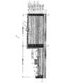
図1は、本発明の第一実施形態に係る半導体装置の模式的な縦断面図を表す。以下、化合物半導体としてIII−V属化合物を用いた例について具体的に説明する。最初にnFET領域4について説明する。化合物半導体基板2としてGaAs単結晶基板を使用した。第1バッファ層5として不純物が添加されていないノンドープのi−GaAs層とした。n型第2障壁層8はn型電荷供給層8aと高抵抗層8bの2層構造を有する。n型電荷供給層8aは、n型不純物としてSiを1.0×10¹²〜4.0×10¹²atoms/cm2の高濃度で添加した厚さ約3nmのn+AlGaAs層から構成され、高抵抗層8bは、不純物が添加されていない厚さ約3nmのi−AlGaAs層から構成されている。第1チャネル層7は、不純物が添加されていない厚さ5nm〜15nmのi−InGaAs層とした。n型電荷供給層8aは第1チャネル層7に電子を供給するために設けられており、高抵抗層8bは、その上の第1チャネル層7との間に良好なヘテロ接合界面を得るために形成されている。(First embodiment)
FIG. 1 is a schematic longitudinal sectional view of a semiconductor device according to the first embodiment of the present invention. Hereinafter, an example using a III-V group compound as a compound semiconductor will be specifically described. First, the
n型第1障壁層6は、n型電荷供給層6aが高抵抗層6b及び高抵抗層6cにより挟まれる3層構造から構成されている。高抵抗層6bは、不純物が添加されていない厚さ約3nmのi−AlGaAs層により形成されている。n型電荷供給層6aは、n型不純物としてSiを1.0×10¹²〜4.0×10¹²atoms/cm2の高濃度で添加された厚さ約6nmのn+AlGaAs層により形成されている。高抵抗層6cは、n型不純物としてSiが1.0×1010〜4.0×1011atoms/cm2の低濃度に添加された厚さ70nm〜200nmのn−AlGaAs層から形成されている。n型電荷供給層6aは、第1チャネル層7に電子を供給するために設けられ、高抵抗層6bは、その下に形成される第1チャネル層7との間に良好なヘテロ接合界面を得るために設けられている。The n-type
p型ゲート領域10は、高抵抗層6cのn−AlGaAs層にZnを拡散したp型領域から形成されている。高抵抗層6cの上面には、シリコン窒化膜からなる絶縁膜9が形成され、p型ゲート領域10にZnを拡散させるための開口部が形成され、その開口部にはゲート電極11が形成されている。ゲート電極11は、チタン(Ti)、白金(Pt)、金(Au)が順次積層された金属電極により構成され、その下部のp型ゲート領域10とオーミックコンタクトがとられている。なお、図1において図示していないが、ゲート電極11を挟むようにソース電極とドレイン電極が形成され、高抵抗層6cとオーミンクコンタクトがとられている。The p-
次に、pFET領域3について説明する。pFET領域3は、高抵抗層6cまでは、nFET領域4と同じ積層構造を備えている。高抵抗層6cの上には、例えばSiなどのn型不純物を6×10¹⁸atoms/cm3含むn+GaAs層のキャップ層26が形成され、その上に不純物が添加されていない厚さ10nm〜100nmのi−GaAs層の第2バッファ層15が形成されている。Next, the
第2チャネル層13は、第2バッファ層15の上に形成され、例えばC(炭素)などのp型不純物を1×10¹⁶〜5×10¹⁸atoms/cm3の濃度で添加された厚さ30nm〜250nmのp−GaAs層から構成されている。ゲートリーク防止層14は、第2チャネル層13の上に形成され、不純物が添加されていない厚さ0nm〜50nmのi−AlGaAs層により構成されている。n型ゲート領域18は、ゲートリーク防止層14の上に形成されるn型第1ゲート層18aとn型第2ゲート層18bの2層構造を備えている。n型第1ゲート層18aは、Siなどのn型不純物を1×1017〜5×1019atoms/cm3の濃度で添加した厚さ10nm〜50nmのn−InGaPから構成されている。n型第2ゲート層18bは、Siなどのn型不純物を1×1017〜5×1019atoms/cm3の濃度で添加した厚さ50〜200nmのn−GaAsにより構成されている。The
ソース領域及びドレイン領域16は、n型ゲート領域18を挟むように離間しゲートリーク防止層14を貫通し、第2チャネル層13の一部領域まで延在するように形成されている。ソース領域及びドレイン領域16は、ゲートリーク防止層14及び第2チャネル層13の一部領域に不純物としてZnを拡散させた拡散領域により構成されている。第2バッファ層15、第2チャネル層13、ゲートリーク防止層14及びn型ゲート領域18の側面と、ゲートリーク防止層14及びn型ゲート領域18の表面にはシリコン窒化膜からなる絶縁膜9が形成されている。絶縁膜9にはソース領域及びドレイン領域16にZnを拡散させるための開口部が形成され、この開口部には金属からなるソース電極及びドレイン電極17が形成され、その下部に形成されるソース領域及びドレイン領域16とオーミックコンタクトがとられている。 The source region and the
素子分離領域12は、pFET領域3とnFET領域4との境界領域であって、n型第2障壁、第1チャネル層7及びn型第1障壁を貫通するように形成されている。素子分離領域12は、B(ボロン)をイオン注入して形成した。 The
以上のとおり、pFET領域3にpn接合型ゲートを有するpチャネルFETを、nFET領域にpn接合型ゲートを有するnチャネルFETを形成した。これにより、両FET、特にpチャネルFETをエンハンスモードで動作させることができ、リーク電流を低減した高速動作の相補型FETを構成することができる。 As described above, a p-channel FET having a pn junction type gate in the
(第二実施形態)
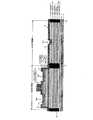
図2は、本発明の第二実施形態に係る半導体装置20の模式的な縦断面図である。同一の部分又は同一の機能を有する部分には同じ符号を付している。(Second embodiment)
FIG. 2 is a schematic longitudinal sectional view of the semiconductor device 20 according to the second embodiment of the present invention. The same parts or parts having the same function are denoted by the same reference numerals.
半導体装置20は、化合物半導体基板2の上に形成したpFET領域3とnFET領域4が形成されている。まず、pFET領域3を説明する。GaAs単結晶からなる化合物半導体基板2の上に、不純物が添加されていないGaAsからなる第1バッファ層5が形成されている。第1バッファ層5の上に、n型不純物が添加されたn+GaAsからなるキャップ層26と不純物が添加されていないi−GaAsからなる第2バッファ層15が形成されている。その上に、p型不純物が添加されたp−GaAsからなる第2チャネル層13が形成されている。In the semiconductor device 20, a
第2チャネル層13上に、不純物が添加されていないi−AlGaAsからなるゲートリーク防止層14が形成されている。その上に、n型不純物が添加されたn−InGaPからなるn型第1ゲート層18aと、n型不純物が添加されたn−GaAsからなるn型第2ゲート層18bの2層構造のn型ゲート領域18が形成されている。ソース領域及びドレイン領域16は、n型ゲート領域18を挟むように離間しゲートリーク防止層14を貫通し、第2チャネル層13の一部領域まで延在するように形成されている。ソース領域及びドレイン領域16は、ゲートリーク防止層14及び第2チャネル層13の一部領域に不純物としてZnを拡散させた拡散領域により構成されている。On the
第2バッファ層15、第2チャネル層13、ゲートリーク防止層14及びn型ゲート領域18の側面と、ゲートリーク防止層14及びn型ゲート領域18の表面にはシリコン窒化膜からなる絶縁膜9が形成されている。絶縁膜9にはソース領域及びドレイン領域16にZnを拡散させるための開口部が形成され、この開口部には金属からなるソース電極及びドレイン電極17が形成され、その下部に形成されるソース領域及びドレイン領域16とオーミックコンタクトがとられている。絶縁膜9は、nFET領域4が形成されていない側面、即ち第2バッファ層15、第2チャネル層13及びゲートリーク防止層14の側面にも形成されている。 The insulating
次に、nFET領域4を説明する。化合物半導体基板2の上に、第1バッファ層5、第2バッファ層15、第2チャネル層13、ゲートリーク防止層14、n型第1ゲート層18a及びn型第2ゲート層18bの積層構造は、pFET領域3と同じ積層構造を備えている。その上に、不純物が添加されていないi-AlGaAsからなる高抵抗層8cと、高濃度のn型不純物が添加されたn+AlGaAsからなるn型電荷供給層8aと、不純物が添加されていないi−AlGaAsからなる高抵抗層8bの3層構造を有するn型第2障壁層8が形成されている。その上に、不純物が添加されていないi−InGaAsからなる第1チャネル層7が形成されている。その上に、不純物が添加されていないi−AlGaAsの高抵抗層6b、高濃度n型不純物が添加されたn+AlGaAsのn型電荷供給層6a、n型不純物が添加されたn−AlGaAsの高抵抗層6cからなる3層構造のn型第1障壁層6が形成されている。Next, the
p型ゲート領域10は、高抵抗層6cのn−AlGaAs層にZnを拡散したp型の領域から形成されている。高抵抗層6cの上面には、シリコン窒化膜からなる絶縁膜9が形成され、p型ゲート領域10にZnを拡散させるための開口部が形成され、その開口部にはゲート電極11が形成されている。ゲート電極11は、チタン(Ti)、白金(Pt)、金(Au)が順次積層された金属電極により構成され、その下部のp型ゲート領域10とオーミックコンタクトがとられている。なお、図2において図示していないが、ゲート電極11を挟むようにソース電極とドレイン電極が形成され、高抵抗層6cとオーミンクコンタクトがとられている。The p-
素子分離領域12は、pFET領域3とnFET領域4との境界領域であって、n型第2障壁、第1チャネル層7及びn型第1障壁を貫通するように形成されている。また、素子分離領域12は、pFET領域3の側面に形成した絶縁膜9の表面、及びnFET領域4の側面、即ち第2バッファ層15、第2チャネル層13、ゲートリーク防止層14、n型ゲート層21、n型第2障壁層8、第1チャネル層7及びn型第1障壁層6の側面にも形成されている。また、絶縁膜9はpFET領域3とnFET領域4の境界領域に形成した素子分離領域12の露出面にも形成されている。 The
なお、各層の膜厚や不純物が添加されている場合の不純物材料、その濃度は、第一実施形態と同様である。 The film thickness of each layer and the impurity material and the concentration when impurities are added are the same as in the first embodiment.
(第三実施形態)
図3〜図11を用いて本発明の第三実施形態に係る半導体装置1の製造方法を説明する。同一の部分又は同一の機能を有する部分には同じ符号を付している。(Third embodiment)
A method for manufacturing the
図3は、GaAs単結晶基板上にGaAs材料を主体とする各層を、例えばMOCVD(Metal Organic Chemical Vapor Deposition)法によりエピタキシャル成長させた積層構造を表す模式的な縦断面図である。GaAs単結晶からなる化合物半導体基板2の上に、不純物を添加しないGaAs層をエピタキシャル成長させて厚さ約200nm程度の第1バッファ層5を形成する。その上に、n型不純物としてSiを1.0×10¹²〜4.0×10¹²atoms/cm2、例えば3.0×1012atoms/cm2の高濃度で添加したn+AlGaAs層をエピタキシャル成長させて厚さ約3nmのn型電荷供給層8aを形成する。次に不純物を添加しないi−AlGaAs層をエピタキシャル成長させて厚さ約3nmの高抵抗層8bを形成する。n型電荷供給層8aと高抵抗層8bによりn型第2障壁層8を構成する。n型第2障壁層8のアルミニウムの組成比は0.2〜0.3、例えばAl0.2Ga0.8Asとする。FIG. 3 is a schematic longitudinal sectional view showing a laminated structure in which each layer mainly composed of GaAs material is epitaxially grown on a GaAs single crystal substrate by, for example, MOCVD (Metal Organic Chemical Vapor Deposition) method. A
次に、n型第2障壁層8の上に不純物を添加しないi−InGaAs層をエピタキシャル成長させて厚さ5nm〜15nmの第1チャネル層7を形成する。第1チャネル層7のインジウム(In)の組成比を0.1〜0.4、例えばIn0.2Ga0.8Asとし、n型第2障壁層8よりもバンドギャップを狭くする。Next, an i-InGaAs layer to which no impurity is added is epitaxially grown on the n-type
次に、第1チャネル層7の上に、不純物を添加しないi−AlGaAs層をエピタキシャル成長させて厚さ約2nmの高抵抗層6bを形成する。次にn型不純物としてSiを1.0×10¹²〜4.0×10¹²atoms/cm2の高濃度に添加したn+AlGaAs層をエピタキシャル成長させて厚さ約6nmのn型電荷供給層6aを形成する。次にn型不純物としてSiを低濃度に添加したn−AlGaAs層をエピタキシャル成長させて厚さ70nm〜200nmの高抵抗層6cを形成する。高抵抗層6b、n型電荷供給層6a及び高抵抗層6cによりn型第1障壁層6とする。n型第1障壁層6のアルミニウムの組成比は0.2〜0.3、例えばAl0.2Ga0.8Asとし、第1チャネル層7よりもバンドギャップを広くする。Next, an i-AlGaAs layer to which no impurity is added is epitaxially grown on the
次に、n型第1障壁層6の上にn型不純物を6×10¹⁸atoms/cm3添加したn+GaAs膜をエピタキシャル成長させてキャップ層26を形成する。次に、不純物を添加しないi−GaAs層をエピタキシャル成長させて厚さ10nm〜100nmの第2バッファ層15を形成する。Next, ann+GaAs film doped with6 × 1018atoms / cm3 of n-type impurities is epitaxially grown on the n-type
次に、第2バッファ層15の上に、例えばCなどのp型不純物を1×10¹⁶〜5×10¹⁸atoms/cm3の濃度で添加したp−GaAs層をエピタキシャル成長させて厚さ30nm〜250nmの第2チャネル層13を形成する。次に、不純物を添加しないi−AlGaAs層をエピタキシャル成長させて厚さ0〜50nmのゲートリーク防止層14を形成する。厚さが0とは、ゲートリーク防止層14は必須の構成ではないためである。ゲートリーク防止層14のアルミニウムの組成比は0.2〜0.3、例えばAl0.2Ga0.8Asとする。Next, ap−GaAs layer to which a p-type impurity such as C is added at a concentration of1 × 1016 to5 × 1018atoms / cm3 is epitaxially grown on the
次に、ゲートリーク防止層14又は第2チャネル層13の上に、Siなどのn型不純物を1×10¹⁷〜5×10¹⁹atoms/cm3の濃度で添加したn−InGaP層をエピタキシャル成長させて厚さ10nm〜50nmのn型第1ゲート層18aを形成する。次に、Siなどのn型不純物を1×1017〜5×1019atoms/cm3添加したn−GaAs層をエピタキシャル成長させて厚さ50〜200nmのn型第2ゲート層18bを形成する。n型第1ゲート層18aとn型第2ゲート層18bによりn型ゲート層21を構成している。なお、以上のエピタキシャル成長は、温度約600℃により行った。Next, ann−InGaP layer to which an n-type impurity such as Si is added at a concentration of1 × 1017 to5 × 1019atoms / cm3 is epitaxially grown on the gate
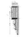
次に、図4に示すように、n型第2ゲート層18b及びn型第1ゲート層18aを選択的にエッチング除去して、pFET領域3にn型ゲート領域18を形成する。フォトリソグラフィ技術及びウエットエッチング若しくはドライエッチング技術を用いてn型ゲート領域18を残す。次に、図5に示すように、ゲートリーク防止層14、第2チャネル層13、第2バッファ層15及びキャップ層26を順次選択的にエッチング除去し、除去した領域をnFET領域4、残した領域をpFET領域3とする。 Next, as shown in FIG. 4, the n-type
次に、図6に示すように、基板上面の露出した表面にプラズマCVD法によりシリコン窒化膜からなる絶縁膜9を厚さ100nm〜500nm形成する。次に、図7に示すように、絶縁膜9に、pFET領域3のソース領域及びドレイン領域形成用の第1開口部22a、22bと、nFET領域4のゲート領域形成用の第1開口部22cを形成する。第1開口部22a、22b、22cはフォトリソグラフィ技術、及び、例えばRIE(Reactive Ion Etching)技術を用いた異方性エッチングにより形成する。 Next, as shown in FIG. 6, an insulating
次に、図8に示すように、絶縁膜9の第1開口部22a、22bを通してゲートリーク防止層14と第2チャネル層13の厚さ方向途中まで拡散させると同時に、第1開口部22cを通して高抵抗層6cの厚さ方向途中まで拡散させる。これにより、pFET領域3にp型のソース領域及びドレイン領域16を、nFET領域4にp型ゲート領域10を形成する。Znは、ジエチルジンク(Zn(C2H5)2)とアルシン(AsH3)を含むガス雰囲気中で基板を約600℃に加熱し、第1開口部22a、22b、22cから導入拡散させる。第1開口部22cのnFET領域4では、Znの拡散の深さを第1チャネル層7の上面から約10nm以上離れるように形成することが好ましい。また、Znはイオン注入法により注入することもきる。Next, as shown in FIG. 8, through the
次に、図9に示すように、pFET領域3とnFET領域4を電気的に分離するための素子分離領域12を形成する。素子分離領域12は、n型第1障壁層6、第1チャネル層7及びn型第2障壁層8の底部に達する深さまで形成する。素子分離領域12は、例えばBイオンのイオン注入法により形成することができる。 Next, as shown in FIG. 9, an
次に、図10に示すように、基板の表面に金属膜を堆積し、フォトリソグラフィ技術及びエッチング技術を用いて選択的に除去して、pFET領域3のソース電極及びドレイン電極17と、nFET領域4のゲート電極11を同時に形成する。金属膜は、例えば電子ビーム蒸着法によりチタン(Ti)、白金(Pt)、金(Au)を例えば30nm、50nm、120nmの厚さで堆積する。これにより、Znを拡散させたp型のソース領域及びドレイン領域16とp型ゲート領域10のそれぞれにおいてオーミックコンタクトをとることができる。 Next, as shown in FIG. 10, a metal film is deposited on the surface of the substrate and selectively removed by using a photolithography technique and an etching technique, so that the source and drain
更に、図11に示すように、基板表面に絶縁材料からなる保護膜25を堆積し、次にnFET領域4のゲート電極11を挟むように保護膜25及び絶縁膜9に第2開口部23を形成する。そして、基板表面に抵抗加熱法により金−ゲルマニウム(AuGe)合金を厚さ約160nm、ニッケル(Ni)を厚さ約40nm堆積し、フォトリソグラフィ技術及びエッチング技術を用いて選択的に除去して、ソース電極及びドレイン電極24を形成する。ソース電極及びドレイン電極24はn型の高抵抗層6cとオーミックコンタクトがとられている。なお、保護膜25及び絶縁膜9の第2開口部23を形成する際に、pFET領域3のn型ゲート領域18の上部にも同時に開口部を形成し、nFET領域4のソース電極及びドレイン電極24と同時に、pFET領域3のゲート電極を形成することができる。 Further, as shown in FIG. 11, a
以上説明した第三実施形態は、図1に示す構造のpチャネルFETとnチャネルFETとを同時に形成する製造方法であるが、同様に図2に示す構造のpチャネルFETとnチャネルFETとを同時に形成することができる。 The third embodiment described above is a manufacturing method in which the p-channel FET and the n-channel FET having the structure shown in FIG. 1 are simultaneously formed. Similarly, the p-channel FET and the n-channel FET having the structure shown in FIG. They can be formed simultaneously.
(第四実施形態)
以下、本発明の第四実施形態に係る半導体装置20の製造方法を説明する。GaAs単結晶からなる化合物半導体基板2の上に、GaAs層の第1バッファ層5をエピタキシャル成長させる。次にn型不純物を高濃度で添加したn+GaAsのキャップ層26と不純物を添加しないi−GaAsの第2バッファ層15をエピタキシャル成長させる。次に、p型不純物を添加したp−GaAsからなる第2チャネル層13と不純物を添加しないi−AlGaAsからなるゲートリーク防止層14をエピタキシャル成長させる。次に、n型不純物を低濃度で添加したn−InGaPからなるn型第1ゲート層18aとn型不純物を添加したn−GaAsからなるn型第2ゲート層18bを順次エピタキシャル成長させてn型ゲート層21を形成する。(Fourth embodiment)
The method for manufacturing the semiconductor device 20 according to the fourth embodiment of the present invention will be described below. A
次に、不純物を添加しないi−AlGaAsからなる高抵抗層8cと、n型不純物を高濃度で添加したn+AlGaAsからなるn型電荷供給層8aと、不純物を添加しないi−AlGaAsからなる高抵抗層8bのn型第2障壁層8を形成する。次に、不純物を添加しないi−InGaAsの第1チャネル層7をエピタキシャル成長させる。次に、不純物を添加しないi−AlGaAsの高抵抗層6b、n型不純物を高濃度で添加したn+AlGaAsのn型電荷供給層6a、n型不純物を低濃度で添加したn−AlGaAsの高抵抗層6cを順次エピタキシャル成長させてn型第1障壁層6を形成する。以上、各層の膜厚や不純物を添加する場合の添加材料や添加濃度は上記第三実施形態と同様である。Next, a high-
次に、素子分離領域12を形成してpFET領域3とnFET領域4とを電気的に分離し、次にpFET領域3の、n型第1障壁層6、第1チャネル層7及びn型第2障壁層8を選択的に除去する。次に、pFET領域3のn型ゲート層21を選択的に除去してn型第1ゲート層18aとn型第2ゲート層18bの積層構造を有するn型ゲート領域18を形成する。 Next, an
次に、シリコン窒化膜から成る絶縁膜9をn型第1障壁層6やゲートリーク防止層14の表面、及び素子分離領域12の表面に堆積する。次に、pFET領域3のソース領域及びドレイン領域形成用、及びnFET領域4のゲート領域形成用の開口部を形成する。そして、この開口部からZnのp型不純物をゲートリーク防止層14及び第2チャネル層13と高抵抗層6cに導入し、pFET領域3にソース領域及びドレイン領域16、nFET領域4にp型ゲート領域10をそれぞれ同時に形成する。 Next, an insulating
次に、金属膜を堆積し選択的に除去して、pFET領域3にソース電極及びドレイン電極17と、nFET領域4にゲート電極11を同時に形成する。その他、pFET領域3のゲート電極やnFET領域4のソース電極及びドレイン電極の形成は、上記第三実施形態と同様に同時に形成することができる。また、エピタキシャル成長により形成した各層の不純物濃度や膜厚、Znの導入拡散、ソース電極、ドレイン電極及びゲート電極の組成や膜厚は、第三実施形態の場合と同様とすることができる。 Next, a metal film is deposited and selectively removed to form a source electrode and a
(第五実施例)
図12は、本発明の第五実施形態に係る半導体装置30の模式的な縦断面図である。上述した同一の部分又は同一の機能を有する部分には同じ符号を付している。また、後述するバックゲート電極31を除き、各層の膜厚や不純物が添加されている場合の不純物材料、その濃度は、第一実施形態と同様である。(Fifth embodiment)
FIG. 12 is a schematic longitudinal sectional view of a
第五実施形態に係る半導体装置30は、上記第一実施形態に係る半導体装置1に対して、pFET領域3にさらにバックゲート電極を31設けている点で異なる。このように、pチャネルFETにバックゲート電極31を設けることにより、相互コンダクタンスが高くなり、pチャネルFETのオン/オフ特性を向上させることができる。 The
図12に示すように、半導体装置30は、化合物半導体基板2の上にpFET領域3とnFET領域4とが形成されている。なお、nFET領域4は、第一実施形態に係る半導体装置1のnFET領域4と同じ構成であり、ここでは説明を省略する。 As shown in FIG. 12, in the
pFET領域3においては、GaAs単結晶からなる化合物半導体基板2の上に、不純物が添加されていないGaAsからなる第1バッファ層5が形成されている。第1バッファ層5の上に、n型第2障壁層8、第1チャネル層7、n型第1障壁層6、キャップ層26、第2バッファ層15、第2チャネル層13が順次形成されている。そして、第2チャネル層13上には、ゲートリーク防止層14やソース領域及びドレイン領域16,16が形成されている。ソース領域及びドレイン領域16は、ゲートリーク防止層14及び第2チャネル層13の一部領域に不純物としてZnを拡散させた拡散領域により構成されている。なお、ゲートリーク防止層14は省略することができる。pFET領域3とnFET領域4とは素子分離領域12により電気的に分離されている。 In the
ゲートリーク防止層14上にはn型ゲート領域18が形成されており、第2チャネル層13に対してpn接合型の電位障壁を有している。そのために、ショットキー型ゲートによる電界効果トランジスタと比較してゲートに印加するゲート電圧を低くしたエンハンスメントモードで駆動することができる。 An n-
さらに、半導体装置30のpFET領域3においては、n型第1障壁層6上にバックゲート電極31が形成されている。バックゲート電極31は、例えば、金−ゲルマニウム(AuGe)合金とニッケル(Ni)との2層構造より形成することができる。このバックゲート電極31は、図示しないが、n型ゲート領域18と電気的に接続される。 Furthermore, a
このバックゲート電極31は、nチャネルFETのソース電極及びドレイン電極24を形成するときに同時に生成することができるため、新たな工程が必要なく、レジストマスクの追加は不要である。 Since the
本出願人は、第一実施形態に係る半導体装置1のpチャネルFETのId−Vg特性と本第五実施形態に係る半導体装置30のpチャネルFETのId−Vg特性の測定を行った。その測定結果を図13に示す。なお、ゲート幅は10μmとした。 The present applicant measured the Id-Vg characteristic of the p-channel FET of the
この図13から、本第五実施形態に係る半導体装置30のpチャネルFETの方が、第一実施形態に係る半導体装置1のpチャネルFETよりも、pチャネルFETのオン/オフ特性が向上していることが分かる。 From FIG. 13, the p-channel FET of the
例えば、第一実施形態に係る半導体装置1のpチャネルFETでは、ゲート電圧Vgが0V時(オン状態)のドレイン電流Idは、4.71×10⁻⁵(A)であり、ゲート電圧Vgが1V時(オフ状態)ドレイン電流Idは、8.23×10⁻⁸(A)である。一方、本第五実施形態に係る半導体装置30のpチャネルFETでは、ゲート電圧Vgが0V時(オン状態)のドレイン電流Idは、5.05×10⁻⁵(A)であり、ゲート電圧Vgが1V時(オフ状態)のドレイン電流Idは、1.75×10⁻¹¹(A)である。For example, in the p-channel FET of the
また、本第五実施形態に係る半導体装置30のpチャネルFETでは、第一実施形態に係る半導体装置1のpチャネルFETに比べて、ゲート電圧Vgが1.5V時のドレイン電流Idは大きくなり、ゲート電圧Vgが−1Vの時のドレイン電流Idは小さくなる。 Also, in the p-channel FET of the
しかも、本第五実施形態に係る半導体装置30のpチャネルFETでは、第一実施形態に係る半導体装置1のpチャネルFETに比べて、ゲート電圧Vgの変化に対するドレイン電流Idの変化率を大きくすることができる。 Moreover, in the p-channel FET of the
このように、pチャネルFETにバックゲート電極31を設けることにより、pチャネルFETのオン/オフ特性を向上させることができる。 Thus, by providing the
なお、バックゲート電極31のレイアウト方法は多数考えられるが、pチャネルFETのn型ゲート領域18、ソース領域及びドレイン領域16が形成された領域の近くにバックゲート電極31を形成することで、レイアウトに関係なく同様の効果が得られる。 Although many layout methods for the
次に、第五実施形態に係る半導体装置30の製造方法を説明する。 Next, a method for manufacturing the
まず、第三実施形態と同様に、図3及び図4で示す工程を行う。なお、これらの工程は第三実施形態と同様であるため、説明を省略する。 First, similarly to the third embodiment, the steps shown in FIGS. 3 and 4 are performed. In addition, since these processes are the same as that of 3rd embodiment, description is abbreviate | omitted.
次に、図14に示すように、pFET領域3のうちバックゲート電極31(図12参照)が形成される領域とnFET領域4において、ゲートリーク防止層14、第2チャネル層13、第2バッファ層15及びキャップ層26を順次選択的にエッチング除去する。 Next, as shown in FIG. 14, in the
次に、第三実施形態と同様に、図6〜図10で示す工程を行う。なお、これらの工程は第三実施形態と同様であるため、説明を省略する。 Next, similarly to the third embodiment, the steps shown in FIGS. 6 to 10 are performed. In addition, since these processes are the same as that of 3rd embodiment, description is abbreviate | omitted.
次に、図15に示すように、基板表面に絶縁材料からなる保護膜25を堆積し、次にnFET領域4のゲート電極11を挟むように保護膜25及び絶縁膜9に第2開口部23を形成する。同時に、pFET領域3においては、n型第1障壁層6のn型の高抵抗層6c上の保護膜25及び絶縁膜9に第3開口部32を形成する。 Next, as shown in FIG. 15, a
そして、基板表面に抵抗加熱法により金−ゲルマニウム(AuGe)合金を厚さ約160nm、ニッケル(Ni)を厚さ約40nm堆積し、フォトリソグラフィ技術及びエッチング技術を用いて選択的に除去して、ソース電極及びドレイン電極24とバックゲート電極31とを同時に形成する。これにより、図12に示すpチャネルFETが形成される。ソース電極及びドレイン電極24はn型の高抵抗層6cとオーミックコンタクトがとられている。また、同様に、バックゲート電極31はn型の高抵抗層6cとオーミックコンタクトがとられている。なお、保護膜25及び絶縁膜9の第2開口部23を形成する際に、pFET領域3のn型ゲート領域18の上部にも同時に開口部を形成し、nFET領域4のソース電極及びドレイン電極24と同時に、pFET領域3のゲート電極を形成することができる。 A gold-germanium (AuGe) alloy with a thickness of about 160 nm and nickel (Ni) with a thickness of about 40 nm is deposited on the surface of the substrate by resistance heating, and selectively removed using a photolithography technique and an etching technique. The source /
このように、バックゲート電極31は、ソース電極及びドレイン電極24を形成するときに同時に形成することができるため、新たな工程が必要なく、レジストマスクの追加は不要である。 As described above, since the
(第六実施例)
図16は、本発明の第六実施形態に係る半導体装置40の模式的な縦断面図である。上述した同一の部分又は同一の機能を有する部分には同じ符号を付している。また、後述するバックゲート電極31及びn−GaAs層41を除き、各層の膜厚や不純物が添加されている場合の不純物材料、その濃度は、第二実施形態と同様である。(Sixth embodiment)
FIG. 16 is a schematic longitudinal sectional view of a
第六実施形態に係る半導体装置40は、上記第二実施形態に係る半導体装置20に対して、第1バッファ層5とキャップ層26との間にn−GaAs層41を形成し、さらに、pFET領域3におけるn−GaAs層41上にバックゲート電極31を設けている点で異なる。このように、pチャネルFETにバックゲート電極31を設けることにより、相互コンダクタンスが高くなり、pチャネルFETのオン/オフ特性を向上させることができる。The
図16に示すように、半導体装置40では、化合物半導体基板2の上にpFET領域3とnFET領域4とが形成されている。なお、nFET領域4は、第二実施形態に係る半導体装置10のnFET領域4と同じ構成であり、ここでは説明を省略する。 As shown in FIG. 16, in the
pFET領域3では、GaAs単結晶からなる化合物半導体基板2の上に、不純物が添加されていないGaAsからなる第1バッファ層5が形成されている。そして、第1バッファ層5の上に、n型不純物としてSiが1.0×10¹⁰〜4.0×10¹¹atoms/cm2の低濃度に添加されたn−GaAsからなるn−GaAs層41が形成される。In the
さらに、このn−GaAs層41上には、半導体装置20と同様に、キャップ層26、第2バッファ層15、第2チャネル層13が順次形成されている。そして、第2チャネル層13上には、ゲートリーク防止層14やソース領域及びドレイン領域16,16が形成されている。ソース領域及びドレイン領域16は、ゲートリーク防止層14及び第2チャネル層13の一部領域に不純物としてZnを拡散させた拡散領域により構成されている。なお、ゲートリーク防止層14は省略することができる。pFET領域3とnFET領域4とは素子分離領域12により電気的に分離されている。Further, the
さらに、半導体装置40においては、n型第1障壁層6上にバックゲート電極31が形成されている。バックゲート電極31は、例えば、金−ゲルマニウム(AuGe)合金とニッケル(Ni)との2層構造より形成することができる。このバックゲート電極31は、図示しないが、n型ゲート領域18と電気的に接続される。 Further, in the
このように、半導体装置40においては、半導体装置30と同様にバックゲート電極31を形成しており、pチャネルFETのオン/オフ特性を向上させることができる。 Thus, in the
次に、第六実施形態に係る半導体装置40の製造方法を説明する。 Next, a method for manufacturing the
まず、GaAs単結晶からなる化合物半導体基板2の上に、GaAs層の第1バッファ層5をエピタキシャル成長させる。次に、n型不純物としてSiが1.0×10¹⁰〜4.0×10¹¹atoms/cm2の低濃度に添加されたn−GaAsからなるn−GaAs層41をエピタキシャル成長させる。その後、第四実施例と同様に、キャップ層26、第2バッファ層15、第2チャネル層13、ゲートリーク防止層14を順次エピタキシャル成長させ、その後、n型第1ゲート層18aとn型第2ゲート層18bを順次エピタキシャル成長させてn型ゲート層21を形成する。First, the
次に、第四実施例と同様に、抵抗層8bと、n型電荷供給層8aと、n型第2障壁層8、第1チャネル層7、n型第1障壁層6を形成し、素子分離領域12を形成してpFET領域3とnFET領域4とを電気的に分離する。 Next, as in the fourth embodiment, the
次に、pFET領域3の、n型第1障壁層6、第1チャネル層7及びn型第2障壁層8を選択的に除去する。さらに、pFET領域3のバックゲート電極形成領域上のゲートリーク防止層14、第2チャネル層13、第2バッファ層15、キャップ層26を選択的に除去する。 Next, the n-type
次に、第四実施例と同様に、n型ゲート領域18を形成し、シリコン窒化膜から成る絶縁膜9をn型第1障壁層6やゲートリーク防止層14の表面、n−GaAs層41の表面、及び素子分離領域12の表面に堆積する。次に、第四実施例と同様に、絶縁膜9を選択的に開口して開口部を形成し、この開口部からZnのp型不純物を導入して、pFET領域3にソース領域及びドレイン領域16、nFET領域4にp型ゲート領域10をそれぞれ同時に形成する。次に、第四実施例と同様に、金属膜を堆積し選択的に除去して、pFET領域3にソース電極及びドレイン電極17と、nFET領域4にゲート電極11を同時に形成する。Next, as in the fourth embodiment, an n-
次に、基板表面に絶縁材料からなる保護膜25を堆積し、nFET領域4のゲート電極11を挟むように保護膜25及び絶縁膜9に第2開口部23を形成する。同時に、pFET領域3においては、n型第1障壁層6のn型の高抵抗層6c上の保護膜25及び絶縁膜9に第3開口部32を形成する。 Next, a
そして、基板表面に抵抗加熱法により金−ゲルマニウム(AuGe)合金を厚さ約160nm、ニッケル(Ni)を厚さ約40nm堆積し、フォトリソグラフィ技術及びエッチング技術を用いて選択的に除去して、ソース電極及びドレイン電極24とバックゲート電極31とを同時に形成する。これにより、図16に示すpチャネルFETが形成される。ソース電極及びドレイン電極24はn型の高抵抗層6cとオーミックコンタクトがとられている。また、同様に、バックゲート電極31はn型の高抵抗層6cとオーミックコンタクトがとられている。なお、保護膜25及び絶縁膜9の第2開口部23を形成する際に、pFET領域3のn型ゲート領域18の上部にも同時に開口部を形成し、nFET領域4のソース電極及びドレイン電極24と同時に、pFET領域3のゲート電極を形成することができる。 A gold-germanium (AuGe) alloy with a thickness of about 160 nm and nickel (Ni) with a thickness of about 40 nm is deposited on the surface of the substrate by resistance heating, and selectively removed using a photolithography technique and an etching technique. The source /
以上のとおり、本発明の半導体装置1、20、30、40の製造方法によれば、化合物半導体基板2上にpチャネルFETとnチャネルFETとを同時に形成することができる。しかも、pチャネルFETのp型の第2チャネル層13に対してn型ゲート領域18とし、またnチャネルFETのn型第1障壁層6に対してp型ゲート領域10とするpn接合型のゲート領域を同時に形成することができる。即ち、エンハンスメントモードの相補型FETを同時に構成することができるので、リーク電流を減少させた高速動作の可能な相補型FETを一つの化合物半導体基板に高密度で製造することが可能となる。 As described above, according to the method for manufacturing the
1、20、30、40 半導体装置
2 化合物半導体基板
3 pチャネル電界効果トランジスタ領域
4 nチャネル電界効果トランジスタ領域
6 n型第1障壁層
7 第1チャネル層
8 n型第2障壁層
9 絶縁膜
10 p型ゲート領域
11 ゲート電極
12 素子分離領域
13 第2チャネル層
15 第2バッファ層
16 ソース領域及びドレイン領域
18 n型ゲート領域
31 バックゲート電極
41n−GaAs層1, 20, 30, 40
Claims (6)
Translated fromJapanese前記化合物半導体基板の上に形成され、第1チャネル層と、前記第1チャネル層にヘテロ接合し、前記第1チャネル層にn型の電荷を供給するn型の第1障壁層と、前記n型の第1障壁層に対してpn接合型の電位障壁を有するp型のゲート領域とを備えるnチャネル電界効果トランジスタ領域と、
前記n型の第1障壁層の上に形成され、p型の第2チャネル層と、ゲートリーク防止層と、前記p型の第2チャネル層に対してpn接合型の電位障壁を有するn型のゲート領域とを含むpチャネル電界効果トランジスタ領域と、から構成され、
前記p型の第2チャネル層には、Znの拡散層からなるp型のソース領域とドレイン領域が、前記n型のゲート領域を挟むように互いに離間して形成され、
前記第1チャネル層は、不純物が添加されていないi−InGaAs層であり、
前記n型の第1障壁層は、前記第1チャネル層の側から順に、前記第1チャネル層との間に良好なヘテロ接合界面を得るために設けられた不純物が添加されていない第1高抵抗層としてのi−AlGaAs層、前記第1チャネル層に電子を供給するために設けられたn型不純物を添加されたn型電荷供給層としてのn+AlGaAs層、n型不純物を添加された第2高抵抗層としてのn−AlGaAs層、の順で積層して形成され、
前記p型のゲート領域は、前記第2高抵抗層にZnを拡散したp型領域で形成され、
前記p型の第2チャネル層は、前記n型の第1障壁層の上に形成されたn型不純物を含むキャップ層としてのn+GaAs層とその上に形成されたバッファ層としての不純物が添加されていないi−GaAs層との上に形成された、p型不純物を添加されたp−GaAs層で構成され、
前記ゲートリーク防止層は、前記p型の第2チャネル層と前記n型のゲート領域との間に、不純物が添加されていないi−AlGaAs層により形成され、
前記n型のゲート領域は、n型不純物を添加したn−InGaPから構成されたn型第1ゲート層と、n型不純物を添加したn−GaAsを前記n型第1ゲート層の上に積層して構成されたn型第2ゲート層との2層構造を備え、
前記p型のソース領域とドレイン領域は、前記ゲートリーク防止層を貫通し、前記第2チャネル層の一部領域まで延在するように、Znを拡散させた拡散領域により構成されている半導体装置。A compound semiconductor substrate;
The n-type first barrier layer formed on the compound semiconductor substrate, heterojunctioned to the first channel layer and supplying n-type charge to the first channel layer, and the n An n-channel field effect transistor region comprising a p-type gate region having a pn junction type potential barrier with respect to the first barrier layer of the type;
Ann-type formed onthe n-type first barrier layer and having a p-type second channel layer, agate leak prevention layer, and a pn junction type potential barrier with respect to the p-type second channel layer and p-channel field effect transistor region and a gate region of,consists,
In the p-type second channel layer, a p-type source region and a drain region made of a Zn diffusion layer are formed apart from each other so as to sandwich the n-type gate region,
The first channel layer is an i-InGaAs layer to which no impurity is added,
The n-type first barrier layer has, in order from the first channel layer side, a first high layer to which an impurity provided to obtain a good heterojunction interface with the first channel layer is not added. An i-AlGaAs layer as a resistance layer, an n+AlGaAs layeras an n-type charge supply layer provided with an n-type impurity provided to supply electrons to the first channel layer, and an n-type impurity as addedAn n−AlGaAslayer as a second high resistance layer isformed in the order of lamination,
The p-type gate region is formed of a p-type region obtained by diffusing Zn in the second high resistance layer,
The p-type second channel layer has an n+GaAs layeras a cap layer containing an n-type impurity formed on the n-type first barrier layer and an impurityas a buffer layer formed thereon. A p-GaAs layerdoped with a p-type impurity formed on an undoped i-GaAs layer;
The gate leak prevention layer is formed of an i-AlGaAs layer to which no impurity is added between the p-type second channel layer and the n-type gate region,
The n-type gate region isformed by stacking an n-type first gate layer made ofn−InGaP doped with n-type impurities and n−GaAsdoped with n-type impurities on then-type first gate layer. A two-layer structure with an n-type second gate layer configured as described above,
The p-type source region and drain region are constituted by a diffusion region in which Zn is diffused so as to penetrate the gate leak prevention layer and extend to a partial region of the second channel layer. .
前記n型の第2障壁層は、前記化合物半導体基板の側から順に、前記第1チャネル層に電子を供給するために設けられたn型不純物を添加されたn型電荷供給層としてのn The n-type second barrier layer is an n-type charge supply layer added with an n-type impurity provided to supply electrons to the first channel layer sequentially from the compound semiconductor substrate side.++AlGaAs層、前記第1チャネル層との間に良好なヘテロ接合界面を得るために設けられた不純物が添加されていない第3高抵抗層としてのi−AlGaAs層、の順で積層して形成されていることを特徴とする請求項1に記載の半導体装置。It is formed by laminating an AlGaAs layer and an i-AlGaAs layer as a third high-resistance layer to which a favorable heterojunction interface is provided between the AlGaAs layer and the first channel layer, to which a good heterojunction interface is not added. The semiconductor device according to claim 1, wherein:
前記化合物半導体基板上に形成され、p型の第2チャネル層と、ゲートリーク防止層と、前記p型の第2チャネル層に対してpn接合型の電位障壁を有するn型のゲート領域とを含むpチャネル電界効果トランジスタ領域と、 A p-type second channel layer formed on the compound semiconductor substrate; a gate leak prevention layer; and an n-type gate region having a pn junction-type potential barrier with respect to the p-type second channel layer. A p-channel field effect transistor region comprising:
前記p型の第2チャネル層の上に形成され、第1チャネル層と、前記第1チャネル層にヘテロ接合し、前記第1チャネル層にn型の電荷を供給するn型の第1障壁層と、前記n型の第1障壁層に対してpn接合型の電位障壁を有するp型のゲート領域とを備えるnチャネル電界効果トランジスタ領域と、から構成され、 An n-type first barrier layer formed on the p-type second channel layer and heterojunction with the first channel layer and supplying the n-type charge to the first channel layer. And an n-channel field effect transistor region comprising a p-type gate region having a pn junction-type potential barrier with respect to the n-type first barrier layer,
前記p型の第2チャネル層には、Znの拡散層からなるp型のソース領域とドレイン領域が、前記n型のゲート領域を挟むように互いに離間して形成され、 In the p-type second channel layer, a p-type source region and a drain region made of a Zn diffusion layer are formed apart from each other so as to sandwich the n-type gate region,
前記p型の第2チャネル層は、p型不純物を添加されたp The p-type second channel layer has a p-type impurity doped p.−−GaAs層で構成され、Composed of GaAs layers,
前記ゲートリーク防止層は、前記p型の第2チャネル層と前記n型のゲート領域との間に、不純物が添加されていないi−AlGaAs層により形成され、 The gate leak prevention layer is formed of an i-AlGaAs layer to which no impurity is added between the p-type second channel layer and the n-type gate region,
前記n型のゲート領域は、n型不純物を添加したn The n-type gate region is doped with n-type impurities.−−InGaPから構成されたn型第1ゲート層と、n型不純物を添加したnAn n-type first gate layer composed of InGaP and n doped with an n-type impurity−−GaAsを前記n型第1ゲート層の上に積層して構成されたn型第2ゲート層との2層構造の一部で構成され、A part of a two-layer structure with an n-type second gate layer formed by laminating GaAs on the n-type first gate layer;
前記p型のソース領域とドレイン領域は、前記ゲートリーク防止層を貫通し、前記第2チャネル層の一部領域まで延在するように、Znを拡散させた拡散領域により構成されており、 The p-type source region and drain region are constituted by diffusion regions in which Zn is diffused so as to penetrate the gate leak prevention layer and extend to a partial region of the second channel layer,
前記第1チャネル層は、前記n型第2ゲート層の上に形成された不純物が添加されていないi−InGaAs層であり、 The first channel layer is an i-InGaAs layer formed on the n-type second gate layer and not doped with impurities.
前記n型の第1障壁層は、前記第1チャネル層の側から順に、前記第1チャネル層との間に良好なヘテロ接合界面を得るために設けられた不純物が添加されていない第1高抵抗層としてのi−AlGaAs層、前記第1チャネル層に電子を供給するために設けられたn型不純物を添加されたn型電荷供給層としてのn The n-type first barrier layer has, in order from the first channel layer side, a first high layer to which an impurity provided to obtain a good heterojunction interface with the first channel layer is not added. An i-AlGaAs layer as a resistance layer, and an n-type charge supply layer added with an n-type impurity provided to supply electrons to the first channel layer++AlGaAs層、n型不純物を添加された第2高抵抗層としてのnN as an AlGaAs layer and a second high resistance layer doped with n-type impurities−−AlGaAs層、の順で積層して形成され、It is formed by laminating in order of AlGaAs layers,
前記p型のゲート領域は、前記第2高抵抗層にZnを拡散したp型領域で形成されている半導体装置。 The p-type gate region is a semiconductor device formed of a p-type region obtained by diffusing Zn in the second high resistance layer.
前記n型の第2障壁層は、前記n型第2ゲート層の側から順に、前記第1チャネル層に電子を供給するために設けられたn型不純物を添加されたn型電荷供給層としてのn The n-type second barrier layer is an n-type charge supply layer doped with an n-type impurity provided to supply electrons to the first channel layer in order from the n-type second gate layer side. N++AlGaAs層、前記第1チャネル層との間に良好なヘテロ接合界面を得るために設けられた不純物が添加されていない第3高抵抗層としてのi−AlGaAs層、の順で積層して形成されていることを特徴とする請求項4に記載の半導体装置。It is formed by laminating an AlGaAs layer and an i-AlGaAs layer as a third high-resistance layer to which a favorable heterojunction interface is provided between the AlGaAs layer and the first channel layer, to which a good heterojunction interface is not added. The semiconductor device according to claim 4, wherein:
Priority Applications (1)
| Application Number | Priority Date | Filing Date | Title |
|---|---|---|---|
| JP2010134698AJP5678485B2 (en) | 2009-08-03 | 2010-06-14 | Semiconductor device |
Applications Claiming Priority (5)
| Application Number | Priority Date | Filing Date | Title |
|---|---|---|---|
| JP2009180653 | 2009-08-03 | ||
| JP2009180653 | 2009-08-03 | ||
| JP2010031710 | 2010-02-16 | ||
| JP2010031710 | 2010-02-16 | ||
| JP2010134698AJP5678485B2 (en) | 2009-08-03 | 2010-06-14 | Semiconductor device |
Publications (2)
| Publication Number | Publication Date |
|---|---|
| JP2011192952A JP2011192952A (en) | 2011-09-29 |
| JP5678485B2true JP5678485B2 (en) | 2015-03-04 |
Family
ID=43526161
Family Applications (1)
| Application Number | Title | Priority Date | Filing Date |
|---|---|---|---|
| JP2010134698AExpired - Fee RelatedJP5678485B2 (en) | 2009-08-03 | 2010-06-14 | Semiconductor device |
Country Status (5)
| Country | Link |
|---|---|
| US (2) | US8378389B2 (en) |
| JP (1) | JP5678485B2 (en) |
| KR (1) | KR101656531B1 (en) |
| CN (1) | CN101989601B (en) |
| TW (1) | TWI497692B (en) |
Families Citing this family (21)
| Publication number | Priority date | Publication date | Assignee | Title |
|---|---|---|---|---|
| JP5678485B2 (en)* | 2009-08-03 | 2015-03-04 | ソニー株式会社 | Semiconductor device |
| JP2013048212A (en)* | 2011-07-28 | 2013-03-07 | Sony Corp | Semiconductor device and semiconductor device manufacturing method |
| WO2015047421A1 (en)* | 2013-09-30 | 2015-04-02 | Hrl Laboratories, Llc | Normally-off iii-nitride transistors with high threshold-voltage and low on-resistance |
| US8669591B2 (en)* | 2011-12-27 | 2014-03-11 | Eta Semiconductor Inc. | E-mode HFET device |
| JP2013179116A (en)* | 2012-02-28 | 2013-09-09 | Sony Corp | Semiconductor device, semiconductor device manufacturing method, protective element, and protective element manufacturing method |
| JP5991018B2 (en)* | 2012-05-16 | 2016-09-14 | ソニー株式会社 | Semiconductor device |
| US9018056B2 (en)* | 2013-03-15 | 2015-04-28 | The United States Of America, As Represented By The Secretary Of The Navy | Complementary field effect transistors using gallium polar and nitrogen polar III-nitride material |
| US20150041820A1 (en)* | 2013-08-12 | 2015-02-12 | Philippe Renaud | Complementary gallium nitride integrated circuits and methods of their fabrication |
| US9437724B2 (en)* | 2014-04-21 | 2016-09-06 | Panasonic Intellectual Property Management Co., Ltd. | Semiconductor device and method of manufacturing the semiconductor device |
| US9406568B2 (en)* | 2014-11-21 | 2016-08-02 | International Business Machines Corporation | Semiconductor structure containing low-resistance source and drain contacts |
| US9299615B1 (en)* | 2014-12-22 | 2016-03-29 | International Business Machines Corporation | Multiple VT in III-V FETs |
| CN105140270B (en)* | 2015-07-29 | 2018-01-09 | 电子科技大学 | A kind of enhanced HEMT device |
| TWI563654B (en)* | 2015-08-26 | 2016-12-21 | Globalwafers Co Ltd | Enhancement-Mode High-Electron-Mobility Transistor Structure |
| WO2017095400A1 (en)* | 2015-12-02 | 2017-06-08 | Intel Corporation | Techniques for co-integrating transition metal dichalcogenide (tmdc)-based and iii-n semiconductor-based transistor devices |
| JPWO2020031636A1 (en)* | 2018-08-09 | 2021-08-12 | ソニーセミコンダクタソリューションズ株式会社 | Semiconductor devices and methods for manufacturing semiconductor devices |
| CN109817523B (en)* | 2018-12-27 | 2021-11-09 | 泉州三安半导体科技有限公司 | Charge balance structure, power device with charge balance structure and manufacturing method |
| CN111564487B (en)* | 2020-05-19 | 2022-06-21 | 南京大学 | AlGaN/GaN MIS-HEMT device based on one-step forming of thick gate dielectric layer electrode and preparation method thereof |
| US11522077B2 (en) | 2020-05-27 | 2022-12-06 | Taiwan Semiconductor Manufacturing Company, Ltd. | Integration of p-channel and n-channel E-FET III-V devices with optimization of device performance |
| CN114420742B (en)* | 2021-11-04 | 2025-10-03 | 西安电子科技大学广州研究院 | Monolithic integrated inverter based on GaN-based enhancement mode device and preparation method thereof |
| US12002857B2 (en)* | 2021-11-30 | 2024-06-04 | Vanguard International Semiconductor Corporation | High electron mobility transistor |
| CN114267747B (en)* | 2021-12-21 | 2023-06-02 | 河北工业大学 | Ga with metal gate structure 2 O 3 AlGaN/GaN solar blind ultraviolet detector and preparation method thereof |
Family Cites Families (17)
| Publication number | Priority date | Publication date | Assignee | Title |
|---|---|---|---|---|
| JPS6167275A (en) | 1984-09-10 | 1986-04-07 | Fujitsu Ltd | semiconductor equipment |
| JPH06101544B2 (en)* | 1985-07-15 | 1994-12-12 | 日本電信電話株式会社 | Complementary field effect transistor and manufacturing method thereof |
| US5250826A (en)* | 1992-09-23 | 1993-10-05 | Rockwell International Corporation | Planar HBT-FET Device |
| JPH06314668A (en)* | 1993-04-30 | 1994-11-08 | Fujitsu Ltd | Plasma etching method and plasma etching apparatus |
| US5479033A (en)* | 1994-05-27 | 1995-12-26 | Sandia Corporation | Complementary junction heterostructure field-effect transistor |
| JPH0864774A (en)* | 1994-08-23 | 1996-03-08 | Fujitsu Ltd | Method for manufacturing semiconductor integrated circuit device |
| JPH08139284A (en)* | 1994-11-04 | 1996-05-31 | Fujitsu Ltd | Semiconductor device and manufacturing method thereof |
| JPH09246532A (en)* | 1996-03-14 | 1997-09-19 | Fujitsu Ltd | Method for manufacturing compound semiconductor device |
| JP3137032B2 (en)* | 1997-05-14 | 2001-02-19 | 日本電気株式会社 | Complementary semiconductor device and method of manufacturing the same |
| US6365925B2 (en) | 1997-09-12 | 2002-04-02 | Sony Corporation | Semiconductor device |
| JPH11150264A (en) | 1997-09-12 | 1999-06-02 | Sony Corp | Semiconductor device, manufacture thereof, and radio communication apparatus |
| JPH1197349A (en)* | 1997-09-19 | 1999-04-09 | Toshiba Corp | Compound semiconductor device and method of manufacturing the same |
| JP4631103B2 (en)* | 1999-05-19 | 2011-02-16 | ソニー株式会社 | Semiconductor device and manufacturing method thereof |
| JP2002222814A (en)* | 2001-01-23 | 2002-08-09 | Sony Corp | Semiconductor device and method of manufacturing the same |
| US7361959B2 (en)* | 2005-11-28 | 2008-04-22 | International Business Machines Corporation | CMOS circuits including a passive element having a low end resistance |
| JP2008060359A (en)* | 2006-08-31 | 2008-03-13 | Sony Corp | Compound semiconductor device |
| JP5678485B2 (en)* | 2009-08-03 | 2015-03-04 | ソニー株式会社 | Semiconductor device |
- 2010
- 2010-06-14JPJP2010134698Apatent/JP5678485B2/ennot_activeExpired - Fee Related
- 2010-07-15KRKR1020100068394Apatent/KR101656531B1/ennot_activeExpired - Fee Related
- 2010-07-15USUS12/805,160patent/US8378389B2/ennot_activeExpired - Fee Related
- 2010-07-16TWTW099123557Apatent/TWI497692B/ennot_activeIP Right Cessation
- 2010-07-27CNCN2010102395394Apatent/CN101989601B/ennot_activeExpired - Fee Related
- 2012
- 2012-06-29USUS13/538,583patent/US8575658B2/enactiveActive
Also Published As
| Publication number | Publication date |
|---|---|
| JP2011192952A (en) | 2011-09-29 |
| TWI497692B (en) | 2015-08-21 |
| KR20110014090A (en) | 2011-02-10 |
| US20120267684A1 (en) | 2012-10-25 |
| US8575658B2 (en) | 2013-11-05 |
| US8378389B2 (en) | 2013-02-19 |
| CN101989601B (en) | 2013-02-27 |
| KR101656531B1 (en) | 2016-09-09 |
| CN101989601A (en) | 2011-03-23 |
| TW201133794A (en) | 2011-10-01 |
| US20110024798A1 (en) | 2011-02-03 |
Similar Documents
| Publication | Publication Date | Title |
|---|---|---|
| JP5678485B2 (en) | Semiconductor device | |
| US10629598B2 (en) | Semiconductor device and manufacturing method of the same | |
| JP4705412B2 (en) | Field effect transistor and manufacturing method thereof | |
| JP6401053B2 (en) | Semiconductor device and manufacturing method of semiconductor device | |
| US8896028B2 (en) | Semiconductor device, manufacturing method thereof, protective element, and manufacturing method thereof | |
| JP2012094774A (en) | Semiconductor device | |
| JP2011066464A (en) | Field effect transistor | |
| KR101172857B1 (en) | Enhancement normally off nitride smiconductor device and manufacturing method thereof | |
| JP2013239735A (en) | Field effect transistor | |
| JP2019009459A (en) | Semiconductor device and manufacturing method of semiconductor device | |
| US20210296311A1 (en) | Semiconductor device and method of manufacturing semiconductor device | |
| TW202141644A (en) | Compound semiconductor apparatus, and method for manufacturing compound semiconductor apparatus | |
| US8076188B2 (en) | Method of manufacturing a semiconductor device | |
| JP2003060078A (en) | Semiconductor device and manufacturing method thereof |
Legal Events
| Date | Code | Title | Description |
|---|---|---|---|
| A621 | Written request for application examination | Free format text:JAPANESE INTERMEDIATE CODE: A621 Effective date:20130522 | |
| A977 | Report on retrieval | Free format text:JAPANESE INTERMEDIATE CODE: A971007 Effective date:20140718 | |
| A131 | Notification of reasons for refusal | Free format text:JAPANESE INTERMEDIATE CODE: A131 Effective date:20140729 | |
| A521 | Request for written amendment filed | Free format text:JAPANESE INTERMEDIATE CODE: A523 Effective date:20140922 | |
| TRDD | Decision of grant or rejection written | ||
| A01 | Written decision to grant a patent or to grant a registration (utility model) | Free format text:JAPANESE INTERMEDIATE CODE: A01 Effective date:20141209 | |
| A61 | First payment of annual fees (during grant procedure) | Free format text:JAPANESE INTERMEDIATE CODE: A61 Effective date:20141222 | |
| R151 | Written notification of patent or utility model registration | Ref document number:5678485 Country of ref document:JP Free format text:JAPANESE INTERMEDIATE CODE: R151 | |
| R250 | Receipt of annual fees | Free format text:JAPANESE INTERMEDIATE CODE: R250 | |
| R250 | Receipt of annual fees | Free format text:JAPANESE INTERMEDIATE CODE: R250 | |
| R250 | Receipt of annual fees | Free format text:JAPANESE INTERMEDIATE CODE: R250 | |
| LAPS | Cancellation because of no payment of annual fees |