JP5677711B2 - Processing gate dielectrics to make high performance metal oxide and metal oxynitride thin film transistors - Google Patents
Processing gate dielectrics to make high performance metal oxide and metal oxynitride thin film transistorsDownload PDFInfo
- Publication number
- JP5677711B2 JP5677711B2JP2011516775AJP2011516775AJP5677711B2JP 5677711 B2JP5677711 B2JP 5677711B2JP 2011516775 AJP2011516775 AJP 2011516775AJP 2011516775 AJP2011516775 AJP 2011516775AJP 5677711 B2JP5677711 B2JP 5677711B2
- Authority
- JP
- Japan
- Prior art keywords
- layer
- plasma
- semiconductor layer
- silicon oxide
- exposing
- Prior art date
- Legal status (The legal status is an assumption and is not a legal conclusion. Google has not performed a legal analysis and makes no representation as to the accuracy of the status listed.)
- Expired - Fee Related
Links
Images


Classifications
- H—ELECTRICITY
- H10—SEMICONDUCTOR DEVICES; ELECTRIC SOLID-STATE DEVICES NOT OTHERWISE PROVIDED FOR
- H10D—INORGANIC ELECTRIC SEMICONDUCTOR DEVICES
- H10D30/00—Field-effect transistors [FET]
- H10D30/60—Insulated-gate field-effect transistors [IGFET]
- H10D30/67—Thin-film transistors [TFT]
- H10D30/674—Thin-film transistors [TFT] characterised by the active materials
- H10D30/6755—Oxide semiconductors, e.g. zinc oxide, copper aluminium oxide or cadmium stannate
- H—ELECTRICITY
- H01—ELECTRIC ELEMENTS
- H01L—SEMICONDUCTOR DEVICES NOT COVERED BY CLASS H10
- H01L21/00—Processes or apparatus adapted for the manufacture or treatment of semiconductor or solid state devices or of parts thereof
- H01L21/02—Manufacture or treatment of semiconductor devices or of parts thereof
- H01L21/02104—Forming layers
- H01L21/02365—Forming inorganic semiconducting materials on a substrate
- H01L21/02518—Deposited layers
- H01L21/02521—Materials
- H01L21/02551—Group 12/16 materials
- H01L21/02554—Oxides
- H—ELECTRICITY
- H01—ELECTRIC ELEMENTS
- H01L—SEMICONDUCTOR DEVICES NOT COVERED BY CLASS H10
- H01L21/00—Processes or apparatus adapted for the manufacture or treatment of semiconductor or solid state devices or of parts thereof
- H01L21/02—Manufacture or treatment of semiconductor devices or of parts thereof
- H01L21/02104—Forming layers
- H01L21/02365—Forming inorganic semiconducting materials on a substrate
- H01L21/02518—Deposited layers
- H01L21/02521—Materials
- H01L21/02565—Oxide semiconducting materials not being Group 12/16 materials, e.g. ternary compounds
- H—ELECTRICITY
- H01—ELECTRIC ELEMENTS
- H01L—SEMICONDUCTOR DEVICES NOT COVERED BY CLASS H10
- H01L21/00—Processes or apparatus adapted for the manufacture or treatment of semiconductor or solid state devices or of parts thereof
- H01L21/02—Manufacture or treatment of semiconductor devices or of parts thereof
- H01L21/02104—Forming layers
- H01L21/02365—Forming inorganic semiconducting materials on a substrate
- H01L21/02612—Formation types
- H01L21/02617—Deposition types
- H01L21/02631—Physical deposition at reduced pressure, e.g. MBE, sputtering, evaporation
- H—ELECTRICITY
- H10—SEMICONDUCTOR DEVICES; ELECTRIC SOLID-STATE DEVICES NOT OTHERWISE PROVIDED FOR
- H10D—INORGANIC ELECTRIC SEMICONDUCTOR DEVICES
- H10D30/00—Field-effect transistors [FET]
- H10D30/01—Manufacture or treatment
- H10D30/021—Manufacture or treatment of FETs having insulated gates [IGFET]
- H10D30/031—Manufacture or treatment of FETs having insulated gates [IGFET] of thin-film transistors [TFT]
- H—ELECTRICITY
- H10—SEMICONDUCTOR DEVICES; ELECTRIC SOLID-STATE DEVICES NOT OTHERWISE PROVIDED FOR
- H10D—INORGANIC ELECTRIC SEMICONDUCTOR DEVICES
- H10D30/00—Field-effect transistors [FET]
- H10D30/60—Insulated-gate field-effect transistors [IGFET]
- H10D30/67—Thin-film transistors [TFT]
- H10D30/6704—Thin-film transistors [TFT] having supplementary regions or layers in the thin films or in the insulated bulk substrates for controlling properties of the device
Landscapes
- Engineering & Computer Science (AREA)
- Microelectronics & Electronic Packaging (AREA)
- Condensed Matter Physics & Semiconductors (AREA)
- General Physics & Mathematics (AREA)
- Manufacturing & Machinery (AREA)
- Computer Hardware Design (AREA)
- Physics & Mathematics (AREA)
- Power Engineering (AREA)
- Thin Film Transistor (AREA)
- Formation Of Insulating Films (AREA)
- Electrodes Of Semiconductors (AREA)
- Physical Vapour Deposition (AREA)
- Chemical Vapour Deposition (AREA)
- Physical Deposition Of Substances That Are Components Of Semiconductor Devices (AREA)
Description
Translated fromJapanese(発明の分野)
本発明の実施形態は、概して、薄膜トランジスタ(TFT)を作る方法に関する。(Field of Invention)
Embodiments of the present invention generally relate to a method of making a thin film transistor (TFT).
(関連技術の説明)
現在、TFTアレイへの関心は特に高く、なぜなら、これらの装置はコンピュータ及びテレビのフラットパネルにしばしば使用される種類のアクティブマトリックス液晶ディスプレイ(LCD)で使用できるからである。LCDには、バックライト照明用の発光ダイオード(LED)も含まれるかもしれない。更に、有機発光ダイオード(OLED)は、アクティブマトリックスディスプレイに使用されてきており、これらのOLEDは、ディスプレイの動作を記述するためにTFTが必要である。(Description of related technology)
At present, the interest in TFT arrays is particularly high because these devices can be used in active matrix liquid crystal displays (LCDs) of the type often used in computer and television flat panels. The LCD may also include a light emitting diode (LED) for backlight illumination. In addition, organic light emitting diodes (OLEDs) have been used in active matrix displays, and these OLEDs require TFTs to describe the operation of the display.
アモルファスシリコンで作られたTFTは、フラットパネルディスプレイ産業の主要なコンポーネントとなった。残念ながら、アモルファスシリコンには、低い移動度などの制約がある。OLEDに必要とされる移動度は、アモルファスシリコンで得られる移動度よりも少なくとも10倍高い。更に、OLEDディスプレイは電流駆動型デバイスであるので、Vthシフトに対してより敏感である。高電流又は高バイアス電圧下のいずれかにおけるアモルファスシリコンTFTのVthシフトは、取り組むべき課題である。他方、ポリシリコンは、アモルファスシリコンよりも高い移動度を有している。ポリシリコンは結晶であり、低い局所的不均一性をもたらす。ポリシリコン膜を作るために複雑なアニーリング処理を必要とするため、アモルファスシリコンとは対照的に、ポリシリコンを使用して大面積ディスプレイを作るのは、より困難であり、又はよりコストが掛かる。アモルファスシリコンの制約のため、OLEDの進歩は遅かった。TFTs made of amorphous silicon have become a major component of the flat panel display industry. Unfortunately, amorphous silicon has limitations such as low mobility. The mobility required for OLEDs is at least 10 times higher than that obtained with amorphous silicon. Furthermore, since OLED displays are current driven devices, they are more sensitive toVth shifts.Vth shift of amorphous silicon TFTs under either high current or high bias voltage is a challenge to be addressed. On the other hand, polysilicon has a higher mobility than amorphous silicon. Polysilicon is crystalline and results in low local inhomogeneities. In contrast to amorphous silicon, making large area displays using polysilicon is more difficult or more costly because it requires a complex annealing process to make the polysilicon film. OLED progress has been slow due to the limitations of amorphous silicon.
近年、酸化亜鉛をアクティブチャネル層として使用する透明なTFTが作られた。酸化亜鉛は、ガラスやプラスチックなどの様々な基板上に比較的低い析出温度で結晶性材料として成長させることができる合成半導体である。 In recent years, transparent TFTs using zinc oxide as the active channel layer have been made. Zinc oxide is a synthetic semiconductor that can be grown as a crystalline material on various substrates such as glass and plastic at a relatively low deposition temperature.
従って、高移動度をもつアモルファスアクティブチャネルを有するTFTに対する技術の必要性がある。 Therefore, there is a need for technology for TFTs having an amorphous active channel with high mobility.
本発明は、概して、TFT及びそれらを製造するための方法を含む。TFTのゲート誘電体層は、TFTの閾値電圧に影響するかもしれない。アクティブチャネル材料を堆積する前にゲート誘電体層を処理することによって、閾値電圧は改善するかもしれない。ゲート誘電体を処理する1つの方法は、N2Oガスにゲート誘電体層を曝露することを含む。ゲート誘電体を処理する別の方法は、N2Oプラズマにゲート誘電体層を曝露することを含む。シリコンベースのTFT用にはゲート誘電体として実用的ではないが、酸化珪素も金属酸化物TFTで使用すると、閾値電圧を改善するかもしれない。ゲート誘電体を処理する、及び/又は、酸化珪素を使用することによって、TFTのサブスレショルドスロープ及び閾値電圧は改善されるかもしれない。The present invention generally includes TFTs and methods for making them. The gate dielectric layer of the TFT may affect the threshold voltage of the TFT. By treating the gate dielectric layer before depositing the active channel material, the threshold voltage may be improved. One method of processing the gate dielectric includes exposing the gate dielectric layer to N2 O gas. Another method of processing the gate dielectric includes exposing the gate dielectric layer to N2 O plasma. Although not practical as a gate dielectric for silicon-based TFTs, the use of silicon oxide in metal oxide TFTs may also improve the threshold voltage. By treating the gate dielectric and / or using silicon oxide, the sub-threshold slope and threshold voltage of the TFT may be improved.
一実施形態では、TFT製造方法を開示している。この方法は、ゲート電極及び基板の上にゲート誘電体層を堆積するステップと、処理のためにN2Oプラズマ又は他のプラズマにゲート誘電体層を曝露するステップと、ゲート誘電体層の上に半導体層を堆積するステップと、半導体層の上に導電層を堆積するステップと、ソース及びドレイン電極及びアクティブチャネルを画定するために導電層及び半導体層をエッチングするステップとを含む。半導体層は、酸素を含み、更に、亜鉛、ガリウム、インジウム、カドミウム、スズ、及びそれらの組み合わせから成る群から選択される1以上の元素を含むか、又は半導体層は、窒素と酸素とを含み、更に、亜鉛、インジウム、スズ、ガリウム、カドミウム、及びそれらの組み合わせから選択される1以上の元素を含む。アクティブチャネルは、半導体層の一部である。In one embodiment, a TFT manufacturing method is disclosed. The method includes depositing a gate dielectric layer over the gate electrode and the substrate, exposing the gate dielectric layer to a N2 O plasma or other plasma for processing, and over the gate dielectric layer. Depositing a semiconductor layer on the semiconductor layer, depositing a conductive layer over the semiconductor layer, and etching the conductive layer and the semiconductor layer to define source and drain electrodes and an active channel. The semiconductor layercomprises oxygen,whereinfurther, zinc, gallium, indium, cadmium, tin, and it contains one or more elements selected from the group consisting of a combination thereof, or the semiconductor layer, nitrogenand oxygenfurther comprising zinc, indium, tin, gallium, cadmium, and one or more elements selected from a combination thereof. The active channel is part of the semiconductor layer.
別の実施形態では、TFTの製造方法を開示している。この方法は、ゲート電極及び基板の上に窒化珪素層を堆積するステップと、窒化珪素層の上に酸化珪素層を堆積するステップと、酸化珪素層の上に半導体層を堆積するステップと、半導体層の上に導電層を堆積するステップと、ソース及びドレイン電極及びアクティブチャネルを画定するために導電層をエッチングするステップとを含む。半導体層は、酸素を含み、更に、亜鉛、ガリウム、インジウム、カドミウム、スズ、及びそれらの組み合わせから成る群から選択される1以上の元素を含むか、又は半導体層は、窒素と酸素とを含み、更に、亜鉛、インジウム、スズ、ガリウム、カドミウム、及びそれらの組み合わせから選択される1以上の元素を含む。アクティブチャネルは、半導体層の一部である。In another embodiment, a method for manufacturing a TFT is disclosed. The method includes depositing a silicon nitride layer over the gate electrode and the substrate; depositing a silicon oxide layer over the silicon nitride layer; depositing a semiconductor layer over the silicon oxide layer; Depositing a conductive layer over the layer and etching the conductive layer to define source and drain electrodes and an active channel. The semiconductor layercomprises oxygen,whereinfurther, zinc, gallium, indium, cadmium, tin, and it contains one or more elements selected from the group consisting of a combination thereof, or the semiconductor layer, nitrogenand oxygenfurther comprising zinc, indium, tin, gallium, cadmium, and one or more elements selected from a combination thereof. The active channel is part of the semiconductor layer.
別の実施形態では、TFTの製造方法を開示している。この方法は、ゲート電極及び基板の上に酸化珪素層を堆積するステップと、酸化珪素層の上に半導体層を堆積するステップと、半導体層の上に導電層を堆積するステップと、ソース及びドレイン電極及びアクティブチャネルを画定するために導電層をエッチングするステップとを含む。半導体層は、酸素を含み、更に、亜鉛、ガリウム、インジウム、カドミウム、スズ、及びそれらの組み合わせから成る群から選択される1以上の元素を含むか、又は半導体層は、窒素と酸素とを含み、更に、亜鉛、インジウム、スズ、ガリウム、カドミウム、及びそれらの組み合わせから選択される1以上の元素を含む。アクティブチャネルは、半導体層の一部を露出する。In another embodiment, a method for manufacturing a TFT is disclosed. The method includes depositing a silicon oxide layer over the gate electrode and the substrate, depositing a semiconductor layer over the silicon oxide layer, depositing a conductive layer over the semiconductor layer, and a source and drain. Etching the conductive layer to define electrodes and active channels. The semiconductor layercomprises oxygen,whereinfurther, zinc, gallium, indium, cadmium, tin, and it contains one or more elements selected from the group consisting of a combination thereof, or the semiconductor layer, nitrogenand oxygenfurther comprising zinc, indium, tin, gallium, cadmium, and one or more elements selected from a combination thereof. The active channel exposes a portion of the semiconductor layer.
別の実施形態では、TFTを開示している。このTFTは、ゲート電極及び基板の上に配置された酸化珪素層と、酸化珪素層の上に配置された半導体層と、半導体層の上に配置されたソース及びドレイン電極とを含む。半導体層は、酸素を含み、更に、亜鉛、ガリウム、インジウム、カドミウム、スズ、及びそれらの組み合わせから成る群から選択される1以上の元素を含むか、又は半導体層は、窒素と酸素とを含み、更に、亜鉛、インジウム、スズ、ガリウム、カドミウム、及びそれらの組み合わせから選択される1以上の元素を含む。ソース及びドレイン電極は、半導体層の一部を露出するために、互いに空間を隔てている。In another embodiment, a TFT is disclosed. The TFT includes a gate electrode and a silicon oxide layer disposed on the substrate, a semiconductor layer disposed on the silicon oxide layer, and source and drain electrodes disposed on the semiconductor layer. The semiconductor layercomprises oxygen,whereinfurther, zinc, gallium, indium, cadmium, tin, and it contains one or more elements selected from the group consisting of a combination thereof, or the semiconductor layer, nitrogenand oxygenfurther comprising zinc, indium, tin, gallium, cadmium, and one or more elements selected from a combination thereof. The source and drain electrodes are separated from each other in order to expose a part of the semiconductor layer.
本発明の上述した構成を詳細に理解することができるように、上記に簡単に要約した本発明のより具体的な説明を実施形態を参照して行う。実施形態のいくつかは添付図面に示されている。しかしながら、添付図面は本発明の典型的な実施形態を示しているに過ぎず、従ってこの範囲を制限していると解釈されるべきではなく、本発明は他の等しく有効な実施形態を含み得ることに留意すべきである。 In order that the above-described structure of the present invention may be understood in detail, a more specific description of the present invention briefly summarized above will be given with reference to the embodiments. Some embodiments are shown in the accompanying drawings. However, the attached drawings only illustrate exemplary embodiments of the present invention and therefore should not be construed as limiting the scope thereof, and the present invention may include other equally effective embodiments. It should be noted.
理解を促進するために、図面に共通する同一の要素を示す際には可能な限り同一の参照番号を使用している。一実施形態に開示される要素を特定の引用なしに他の実施形態に有益に組み込んでもよいと理解される。 To facilitate understanding, identical reference numerals have been used, where possible, to designate identical elements that are common to the drawings. It is understood that elements disclosed in one embodiment may be beneficially incorporated into other embodiments without specific citations.
本発明は、概して、TFT及びそれらを製造するための方法を含む。TFTのゲート誘電体層は、TFTの閾値電圧に影響するかもしれない。アクティブチャネル材料を堆積する前にゲート誘電体層を処理することによって、閾値電圧は改善するかもしれない。ゲート誘電体を処理する1つの方法は、摂氏200度より高い温度でN2Oガスにゲート誘電体層を曝露するステップを含む。ゲート誘電体を処理する別の方法は、N2Oプラズマにゲート誘電体層を曝露するステップを含む。シリコンベースのTFT用にはゲート誘電体として実用的ではないが、酸化珪素も金属酸化物TFTで使用すると、閾値電圧を改善するかもしれない。ゲート誘電体を処理する、及び/又は、酸化珪素を使用することによって、TFTの閾値電圧は改善されるかもしれない。ドーピングを通してアモルファス材料として酸化亜鉛ベースの半導体を作ることができる。従って、それは粒子構造の結果と考えられる不均一性の問題を回避するだろう。ボトムゲート型TFT構造を使用することによって、酸化亜鉛ベースの半導体などのアモルファス半導体は、現在のディスプレイ製造プロセスでより容易に実行される。The present invention generally includes TFTs and methods for making them. The gate dielectric layer of the TFT may affect the threshold voltage of the TFT. By treating the gate dielectric layer before depositing the active channel material, the threshold voltage may be improved. One method of processing the gate dielectric includes exposing the gate dielectric layer to N2 O gas at a temperature greater than 200 degrees Celsius. Another method of processing the gate dielectric includes exposing the gate dielectric layer to N2 O plasma. Although not practical as a gate dielectric for silicon-based TFTs, the use of silicon oxide in metal oxide TFTs may also improve the threshold voltage. By treating the gate dielectric and / or using silicon oxide, the threshold voltage of the TFT may be improved. Zinc oxide based semiconductors can be made as amorphous materials through doping. Therefore, it will avoid the problem of non-uniformity that can be attributed to particle structure. By using a bottom gate TFT structure, amorphous semiconductors such as zinc oxide based semiconductors are more easily implemented in current display manufacturing processes.
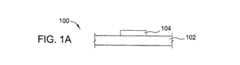
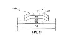
図1A〜1Fは、様々な製造段階における本発明の一実施形態に係るTFT100の概略断面図である。TFTは基板102を含んでもよい。一実施形態では、基板102はガラスを含んでもよい。別の実施形態では、基板102はポリマーを含んでもよい。別の実施形態では、基板102はプラスチックを含んでもよい。更に別の実施形態では、基板102は金属を含んでもよい。 1A to 1F are schematic cross-sectional views of a
基板上に、ゲート電極104を形成してもよい。ゲート電極104は、TFT内で荷電粒子の動きを制御する導電層を含んでもよい。ゲート電極104は、アルミニウム、タングステン、クロム、タンタル、又はそれらの組み合わせなどの金属を含んでもよい。ゲート電極104は、スパッタリング、リソグラフィー、及びエッチングを含む従来の堆積技術を使用して形成してもよい。ゲート電極104は、基板102上に導電層を堆積させる被覆(ブランケット)によって形成してもよい。導電層はスパッタリングによって堆積してもよい。その後、フォトレジスト層を導電層の上に堆積してもよい。フォトレジスト層は、マスクを形成するためにパターニングしてもよい。ゲート電極104は、基板102の上にゲート電極104を残すために導電層のマスクされていない部分をエッチングで取り除くことによって形成してもよい。 A
ゲート電極104の上に、ゲート誘電体層106を堆積してもよい。ゲート誘電体層106は、TFTのサブスレッショルドスイング又はスロープ及び閾値電圧に影響する。シリコンベースのTFT(即ち、アモルファスシリコンなどのシリコンベースの半導体を有するTFT)において、酸化珪素は非常に正のVthと低い移動度を有したTFTをもたらすので、ゲート誘電体層106は酸化珪素を含むことができない。しかしながら、金属酸化物TFTに対して、酸化珪素が有効なゲート誘電体層106として機能するかもしれないことが発見された。酸化珪素の中の酸素は、金属酸化物層を効果的に変化させたり又は相互作用する可能性は無いので、TFTが動作しない可能性は無い。一実施形態では、ゲート誘電体層106は窒化珪素を含んでもよい。別の実施形態では、ゲート誘電体層106は酸化珪素を含んでもよい。別の実施形態では、ゲート誘電体層106は二酸化珪素を含んでもよい。別の実施形態では、ゲート誘電体層106は酸窒化珪素を含んでもよい。別の実施形態では、ゲート誘電体層106はAl2O3を含んでもよい。ゲート誘電体層106は、プラズマCVD(PECVD)を含むよく知られた堆積技術で堆積してもよい。一実施形態では、ゲート誘電体層106は物理的気相成長法(PVD)によって堆積してもよい。A
ゲート誘電体層106が堆積された後に、ゲート誘電体層106を処理してもよい。ゲート誘電体層106を処理する様々な技術を以下で詳細に議論する。技術のうちの1つは、ゲート誘電体層106の表面をパッシベーションするために、ゲート誘電体層106をプラズマ108に曝露することを含む。 After the
ゲート誘電体層106を処理した後に、半導体層110をその上に堆積してもよい。半導体層110は、最終的なTFT構造にアクティブチャネルを含む材料となるだろう。半導体層110は、酸素を含み、更に、亜鉛、ガリウム、カドミウム、インジウム、スズ、及びそれらの組み合わせから成る群から選択される1以上の元素を含んでもよく、又は、窒素と酸素とを含み、更に、亜鉛、インジウム、スズ、ガリウム、カドミウム、及びそれらの組み合わせから成る群から選択される1以上の元素を含んでもよい。一実施形態では、半導体層110は、酸素、窒素、及び、満ちたs軌道及び満ちたd軌道を有する1以上の元素を含んでもよい。別の実施形態では、半導体層110は、酸素、窒素、及び満ちたf軌道を有する1以上の元素を含んでもよい。別の実施形態では、半導体層110は、酸素、窒素、及び1以上の2価の元素を含んでもよい。別の実施形態では、半導体層110は、酸素、窒素、及び1以上の3価の元素を含んでもよい。別の実施形態では、半導体層は、酸素、窒素、及び1以上の4価の元素を含んでもよい。
After processing the
また、半導体層110は、ドーパントを含んでもよい。使用可能な適当なドーパントは、Al、Sn、Ga、Ca、Si、Ti、Cu、Ge、In、Ni、Mn、Cr、V、Mg、SixNy、AlxOy、SiCを含む。一実施形態では、ドーパントはアルミニウムを含む。別の実施形態では、ドーパントはスズを含む。In addition, the
半導体層110の例は以下を含む:ZnOxNy、SnOxNy、InOxNy、CdOxNy、GaOxNy、ZnSnOxNy、ZnInOxNy、ZnCdOxNy、ZnGaOxNy、SnInOxNy、SnCdOxNy、SnGaOxNy、InCdOxNy、InGaOxNy、CdGaOxNy、ZnSnInOxNy、ZnSnCdOxNy、ZnSnGaOxNy、ZnInCdOxNy、ZnInGaOxNy、ZnCdGaOxNy、SnInCdOxNy、SnInGaOxNy、SnCdGaOxNy、InCdGaOxNy、ZnSnInCdOxNy、ZnSnInGaOxNy、ZnInCdGaOxNy、及びSnInCdGaOxNy。半導体層110の例は以下のドープされた材料を含む:ZnOxNy:Al、ZnOxNy:Sn、SnOxNy:Al、InOxNy:Al、InOxNy:Sn、CdOxNy:Al、CdOxNy:Sn、GaOxNy:Al、GaOxNy:Sn、ZnSnOxNy:Al、ZnInOxNy:Al、ZnInOxNy:Sn、ZnCdOxNy:Al、ZnCdOxNy:Sn、ZnGaOxNy:Al、ZnGaOxNy:Sn、SnInOxNy:Al、SnCdOxNy:Al、SnGaOxNy:Al、InCdOxNy:Al、InCdOxNy:Sn、InGaOxNy:Al、InGaOxNy:Sn、CdGaOxNy:Al、CdGaOxNy:Sn、ZnSnInOxNy:Al、ZnSnCdOxNy:Al、ZnSnGaOxNy:Al、ZnInCdOxNy:Al、ZnInCdOxNy:Sn、ZnInGaOxNy:Al、ZnInGaOxNy:Sn、ZnCdGaOxNy:Al、ZnCdGaOxNy:Sn、SnInCdOxNy:Al、SnInGaOxNy:Al、SnCdGaOxNy:Al、InCdGaOxNy:Al、InCdGaOxNy:Sn、ZnSnInCdOxNy:Al、ZnSnInGaOxNy:Al、ZnInCdGaOxNy:Al、ZnInCdGaOxNy:Sn、及びSnInCdGaOxNy:Al。Examples of the semiconductor layer 110 include: ZnOx Ny , SnOx Ny , InOx Ny , CdOx Ny , GaOx Ny , ZnSnOx Ny , ZnInOx Ny , ZnCdOx Ny , ZnGaOx Ny , SnInOx Ny , SnCdOx Ny , SnGaOx Ny , InCdOx Ny , InGaOx Ny , CdGaOx Ny , ZnSnInOx Ny , ZnSnInOx Ny , ZnSnInOx Ny , ZnSnInOx NyZnInCdO x N y, ZnInGaO x N y, ZnCdGaO x N y, SnInCdO x N y, SnInGaO x N y, SnCdGaO x N y, InCdGaO x N y, ZnSnInCdO x N y, ZnSnInGaO x N y, ZnInCdGaO x N y, And SnIn CdGaOx Ny . Examples of the semiconductor layer 110 include the following doped materials: ZnOx Ny : Al, ZnOx Ny : Sn, SnOx Ny : Al, InOx Ny : Al, InOx Ny : Sn,CdO x N y: Al, CdO x N y: Sn, GaO x N y: Al, GaO x N y: Sn, ZnSnO x N y: Al, ZnInO x N y: Al, ZnInO x N y: Sn, ZnCdOx N y: Al, ZnCdO x N y: Sn, ZnGaO x N y: Al, ZnGaO x N y: Sn, SnInO x N y: Al, SnCdO x N y: Al, SnGaO x N y: Al, InCdO xN y: Al, InCdO x N y: Sn, InGaO x N y: Al, InGaO x N y: Sn, CdGaO x N y: Al, CdGaO xN y: Sn, ZnSnInO x N y: Al, ZnSnCdO x N y: Al, ZnSnGaO x N y: Al, ZnInCdO x N y: Al, ZnInCdO x N y: Sn, ZnInGaO x N y: Al, ZnInGaO x Ny: Sn, ZnCdGaO x N y : Al, ZnCdGaO x N y: Sn, SnInCdO x N y: Al, SnInGaO x N y: Al, SnCdGaO x N y: Al, InCdGaO x N y: Al, InCdGaO x N y: Sn, ZnSnInCdO x N y: Al, ZnSnInGaO x N y: Al, ZnInCdGaO x N y: Al, ZnInCdGaO x N y: Sn, and SnInCdGaOx Ny: Al.
半導体層110は、スパッタリングによって堆積してもよい。一実施形態では、スパッタリングターゲットは、亜鉛、ガリウム、スズ、カドミウム、インジウム、又はそれらの組み合わせなどの金属を含む。スパッタリングターゲットは、ドーパントを更に含んでもよい。反応性スパッタリングによって半導体層110を堆積するために、酸素含有ガス及び窒素含有ガスがチャンバ内に導入される。一実施形態では、窒素含有ガスは、N2を含む。別の実施形態では、窒素含有ガスは、N2O、NH3、又はそれらの組み合わせを含む。一実施形態では、酸素含有ガスは、O2を含む。別の実施形態では、酸素含有ガスは、N2Oを含む。窒素含有ガスの窒素と酸素含有ガスの酸素は、金属、酸素、窒素、及び任意にドーパントを基板上に含む半導体材料を形成するために、スパッタリングターゲットからの金属と反応する。一実施形態では、窒素含有ガスと酸素含有ガスは、別々のガスである。別の実施形態では、窒素含有ガスと酸素含有ガスは、同じガスを含む。また、スパッタリングの間、B2H6、CO2、CO、CH4、及びそれらの組み合わせなどの追加添加物をチャンバに提供してもよい。The
半導体層110を堆積した後に、導電層112を堆積してもよい。一実施形態では、導電層112は、アルミニウム、タングステン、モリブデン、クロム、タンタル、及びそれらの組み合わせなどの金属を含んでもよい。導電層112は、PVDを使用することによって堆積してもよい。 The
ソース電極114、ドレイン電極116、及びアクティブチャネル118は、導電層112を堆積した後に、導電層112の一部をエッチングで除去することによって画定してもよい。半導体層110の一部もエッチングによって除去してもよい。図示されていないが、導電層を堆積する前に、エッチストップ層を半導体層110の上に堆積してもよい。エッチストップ層は、エッチングの間、過度のプラズマ曝露からアクティブチャネル118を保護するために機能する。
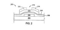
図2は、本発明の別の実施形態に係るTFT200の概略断面図である。TFT200は、基板202の上に配置されたゲート電極204を含む。ソース電極212、ドレイン電極214、アクティブチャネル216、及び半導体層210も存在する。多層ゲート誘電体が存在する。ゲート誘電体は、第1ゲート誘電体層206及び第2ゲート誘電体層208を有してもよい。一実施形態では、第1ゲート誘電体層206は、窒化珪素を含んでもよい。一実施形態では、第2ゲート誘電体層208は、酸化珪素を含んでもよい。上述のように、酸化珪素はシリコンベースのTFTで使用可能ではないが、金属酸化物TFTでは有益かもしれない。 FIG. 2 is a schematic cross-sectional view of a
表1は、ゲート誘電体層上で実行される処理を除いて実質的に同じいくつかのTFTの比較を示す。各実施例において、ゲート誘電体層は窒化珪素である。
窒化珪素のゲート誘電体層を備えて作られたTFTは、未処置のままであった。ゲート誘電体層の堆積後に、ゲート誘電体層を大気に曝露させずに、半導体層をその上に堆積した。TFTの移動度は9.78cm2/V−sであり、サブスレショルドスロープは2V/decであった。TFTs made with a silicon nitride gate dielectric layer remained untreated. After deposition of the gate dielectric layer, the semiconductor layer was deposited thereon without exposing the gate dielectric layer to the atmosphere. The mobility of the TFT was 9.78 cm2 / V-s, and the subthreshold slope was 2 V / dec.
窒化珪素のゲート誘電体層と、その上に酸化珪素の層を堆積したTFTが作られた。ゲート誘電体層の更なる処理は行わなかった。酸化珪素層の堆積後に、ゲート誘電体層又は酸化珪素を大気に曝露させずに、半導体層をその上に堆積した。TFTの移動度は7.65cm2/V−sであり、サブスレショルドスロープは1.48V/decであった。A TFT was fabricated with a silicon nitride gate dielectric layer and a silicon oxide layer deposited thereon. No further processing of the gate dielectric layer was performed. After deposition of the silicon oxide layer, a semiconductor layer was deposited thereon without exposing the gate dielectric layer or silicon oxide to the atmosphere. The mobility of the TFT was 7.65 cm2 / V-s, and the subthreshold slope was 1.48 V / dec.
窒化珪素のゲート誘電体を備えたTFTが作られ、N2Oのプラズマに曝露された。ゲート誘電体層を大気に曝露させず、半導体層をその上に堆積した。TFTの移動度は7.84cm2/V−sであり、サブスレショルドスロープは1.42V/decであった。A TFT with a silicon nitride gate dielectric was fabricated and exposed to a N2 O plasma. The gate dielectric layer was not exposed to the atmosphere and a semiconductor layer was deposited thereon. The mobility of the TFT was 7.84 cm2 / V-s, and the subthreshold slope was 1.42 V / dec.
窒化珪素のゲート誘電体を備えたTFTが作られ、PH3のプラズマに曝露された。ゲート誘電体層を大気に曝露させず、半導体層をその上に堆積した。TFTの移動度は1cm2/V−s未満であり、サブスレショルドスロープは4V/decを超えていた。A TFT with a silicon nitride gate dielectric was fabricated and exposed to a PH3 plasma. The gate dielectric layer was not exposed to the atmosphere and a semiconductor layer was deposited thereon. The mobility of the TFT was less than 1 cm2 / V-s, and the subthreshold slope exceeded 4 V / dec.
窒化珪素のゲート誘電体を備えたTFTが作られ、NH3のプラズマに曝露された。ゲート誘電体層を大気に曝露させず、半導体層をその上に堆積した。TFTの移動度は6.28cm2/V−sであり、サブスレショルドスロープは2.34V/decであった。A TFT with a silicon nitride gate dielectric was fabricated and exposed to NH3 plasma. The gate dielectric layer was not exposed to the atmosphere and a semiconductor layer was deposited thereon. The mobility of the TFT was 6.28 cm2 / V-s, and the subthreshold slope was 2.34 V / dec.
窒化珪素のゲート誘電体を備えたTFTが作られ、H2のプラズマに曝露された。ゲート誘電体層を大気に曝露させず、半導体層をその上に堆積した。TFTの移動度は2.5cm2/V−sであり、サブスレショルドスロープは2.8V/decであった。A TFT with a silicon nitride gate dielectric was fabricated and exposed to a H2 plasma. The gate dielectric layer was not exposed to the atmosphere and a semiconductor layer was deposited thereon. The mobility of the TFT was 2.5 cm2 / V-s, and the subthreshold slope was 2.8 V / dec.
窒化珪素のゲート誘電体を備えたTFTが作られ、アルゴンのプラズマに曝露された。ゲート誘電体層を大気に曝露させず、半導体層をその上に堆積した。TFTの移動度は2.9cm2/V−sであり、サブスレショルドスロープは2.8V/decであった。A TFT with a silicon nitride gate dielectric was fabricated and exposed to an argon plasma. The gate dielectric layer was not exposed to the atmosphere and a semiconductor layer was deposited thereon. The mobility of the TFT was 2.9 cm2 / V-s, and the subthreshold slope was 2.8 V / dec.
窒化珪素のゲート誘電体を備えたTFTが作られ、大気に曝露された。その後、半導体層を窒化珪素の上に堆積した。TFTの移動度は6.2cm2/V−sであり、サブスレショルドスロープは1.84V/decであった。A TFT with a silicon nitride gate dielectric was fabricated and exposed to the atmosphere. Thereafter, a semiconductor layer was deposited on the silicon nitride. The mobility of the TFT was 6.2 cm2 / V-s, and the subthreshold slope was 1.84 V / dec.
窒化珪素のゲート誘電体を備えたTFTが作られ、N2のプラズマに曝露された。ゲート誘電体層を大気に曝露させず、半導体層をその上に堆積した。TFTの移動度は2.9cm2/V−sであり、サブスレショルドスロープは2.8V/decであった。A TFT with a silicon nitride gate dielectric was fabricated and exposed to a N2 plasma. The gate dielectric layer was not exposed to the atmosphere and a semiconductor layer was deposited thereon. The mobility of the TFT was 2.9 cm2 / V-s, and the subthreshold slope was 2.8 V / dec.
上記実施例に示されるように、ゲート誘電体層の処理は、サブスレショルドスロープ及び移動度に影響するかもしれない。窒化珪素層の上の追加酸化珪素層は、良好な移動度及び非常に良好なサブスレショルドスロープを有するTFTを生み出した。更に、N2Oプラズマ処理は、良好な移動度及び非常に良好なサブスレショルドスロープを有するTFTを生み出した。酸化珪素TFTに対する移動度及びN2Oプラズマは両者とも未処理のままのTFTを下回ったが、サブスレショルドスロープはかなりより良好であった。逆に、アルゴンプラズマ、H2プラズマ、NH3プラズマ、又はN2プラズマによる処理は、サブスレショルドスロープをはるかに悪化させる。従って、ゲート誘電体層上で実行される処理の種類は、TFTの性能に影響する。N2Oプラズマ中の酸素が窒化珪素を減少させるか、又は珪素窒素結合を切断して表面を不動態化させると信じられている。As shown in the above example, the processing of the gate dielectric layer may affect the subthreshold slope and mobility. The additional silicon oxide layer on top of the silicon nitride layer produced TFTs with good mobility and very good subthreshold slope. Furthermore, the N2 O plasma treatment yielded TFTs with good mobility and very good subthreshold slope. Both mobility and N2 O plasma for silicon oxide TFTs were below that of the untreated TFT, but the subthreshold slope was much better. Conversely, treatment with argon plasma, H2 plasma, NH3 plasma, or N2 plasma makes the subthreshold slope much worse. Thus, the type of processing performed on the gate dielectric layer affects the performance of the TFT. It is believed that oxygen in the N2 O plasma reduces silicon nitride or breaks the silicon nitrogen bond and passivates the surface.
図3は、本発明の一実施形態に係るアクティブレイヤ材料の堆積前にゲート誘電体層をプラズマ処理に曝露する効果を示すグラフである。未処理、N2Oプラズマ曝露、N2Oプラズマに続いてH2プラズマ曝露、及びN2Oプラズマに続いてNH3プラズマ曝露の、4つの別々の結果が図3に示されている。上記実施例に示されるように、H2プラズマかNH3プラズマのいずれか単独によるゲート誘電体層の処理は良好な結果を示さないが、N2Oプラズマの後にH2プラズマかNH3プラズマのいずれかにゲート誘電体層を曝露することによって、単独のN2Oプラズマ処理に匹敵するサブスレショルドスロープを生み出すことが可能である。FIG. 3 is a graph illustrating the effect of exposing a gate dielectric layer to a plasma treatment prior to deposition of an active layer material according to an embodiment of the present invention. Four separate results are shown in FIG. 3, untreated, N2 O plasma exposure, N2 O plasma followed by H2 plasma exposure, and N2 O plasma followed by NH3 plasma exposure. As shown in the above example, the treatment of the gate dielectric layer with either H2 plasma or NH3 plasma alone does not give good results, but after N2 O plasma, the H2 plasma or NH3 plasma By exposing the gate dielectric layer to either, it is possible to create a subthreshold slope comparable to a single N2 O plasma treatment.
追加的なゲート誘電体処理も模索されてきた。例えば、ゲート誘電体層をプラズマ無しのN2Oガスに曝露した後に、N2Oプラズマに曝露してもよい。Additional gate dielectric processing has also been explored. For example, the gate dielectric layer may be exposed to N2 O plasma without plasma and then exposed to N2 O plasma.
図4Aは、本発明の一実施形態に係るゲート誘電体層の析出温度の効果を示すグラフである。図4Aに示されるように、摂氏350度で堆積した窒化珪素ゲート誘電体層又は摂氏400度で堆積しアニール処理した酸化珪素ゲート誘電体層と比較して、摂氏200度で堆積した窒化珪素ゲート誘電体層は、より正のVthを有する。しかしながら、酸化珪素TFTは、より小さいサブスレショルドスロープを有する。FIG. 4A is a graph illustrating the effect of the deposition temperature of the gate dielectric layer according to one embodiment of the present invention. As shown in FIG. 4A, a silicon nitride gate dielectric layer deposited at 200 degrees Celsius compared to a silicon nitride gate dielectric layer deposited at 350 degrees Celsius or a silicon oxide gate dielectric layer deposited and annealed at 400 degrees Celsius. The dielectric layer has a more positiveVth . However, silicon oxide TFTs have a smaller subthreshold slope.
図4Bは、本発明の一実施形態に係るゲート誘電体層をNH3に曝露する効果を示すグラフである。図4Bに示されるように、摂氏350度で堆積しNH3に曝露した窒化珪素ゲート誘電体層と比較して、摂氏200度で堆積しNH3に曝露した窒化珪素ゲート誘電体層は、より正のVth及びより低いサブスレショルドスロープを有する。FIG. 4B is a graph illustrating the effect of exposing a gate dielectric layer to NH3 according to one embodiment of the invention. As shown in FIG. 4B, compared to a silicon nitride gate dielectric layer deposited at 350 degrees Celsius and exposed to NH3 , the silicon nitride gate dielectric layer deposited at 200 degrees Celsius and exposed to NH3 is more It has a positiveVth and a lower subthreshold slope.
図5は、本発明の一実施形態に係るアクティブレイヤ材料の堆積前のゲート誘電体層へのN2Oプラズマ処理の効果を示すグラフである。表2は、図5に示された3つのTFTに対する移動度及びサブスレショルドスロープ値を示す。FIG. 5 is a graph illustrating the effect of N2 O plasma treatment on a gate dielectric layer before deposition of an active layer material according to an embodiment of the present invention. Table 2 shows the mobility and subthreshold slope values for the three TFTs shown in FIG.
図5のTFTにおいて、夫々は摂氏200度で窒化珪素ゲート誘電体層を堆積した。TFT2は、半導体層を堆積する前にN2Oプラズマによってゲート誘電体層を処理して作られた。TFT2は、半導体層の堆積前にN2Oプラズマで処理しなかったTFT1及び3と比較して、より高い移動度及びより低いサブスレショルドスロープを有していた。非プラズマ処理TFT間の違いは、TFT3は4ヶ月経過していたことである。In the TFT of FIG. 5, each deposited a silicon nitride gate dielectric layer at 200 degrees Celsius. TFT2 was made by treating the gate dielectric layer with N2 O plasma before depositing the semiconductor layer.
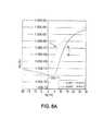
図6A及び6Bは、本発明の一実施形態に係るアクティブレイヤ材料の堆積前に、ゲート誘電体層をN2Oに曝露し、N2Oプラズマ処理した効果を示すグラフである。表3は、図6A及び6Bに示される4つの基板に対するサブスレショルドスロープ及び飽和移動度を示す。
N2O処理は、堆積したゲート誘電体層をN2Oガスに曝露するステップを含んでいた。N2O洗浄は、堆積したゲート誘電体層をN2Oプラズマに曝露するステップを含んでいた。N2O洗浄は、N2O処理よりも強力な効果を有する。しかしながら、N2Oは、Ioffを低下させる。N2O洗浄及びN2Oは共にサブスレショルドスロープを低下させた。しかしながら、N2O洗浄とN2O処理の両方を行うと、サブスレショルドスロープは更に低下した。N2O洗浄とN2O処理の両方を行うと、飽和移動度もかなり減少した。表3に示されるように、N2O洗浄が実行されると、未処理又はN2O処理と比較して、Vgは10Vdsではるかに高い。The N2 O treatment included exposing the deposited gate dielectric layer to N2 O gas. The N2 O clean involved exposing the deposited gate dielectric layer to N2 O plasma. N2 O cleaning has a stronger effect than N2 O treatment. However, N2 O reduces Ioff . N2 O wash and N2 O both lowered the subthreshold slope. However, when both N2 O cleaning and N2 O treatment were performed, the subthreshold slope further decreased. When both N2 O cleaning and N2 O treatment were performed, the saturation mobility was also significantly reduced. As shown in Table 3, Vg is much higher at 10 Vds when N2 O cleaning is performed compared to untreated or N2 O treatment.
図7A及び7Bは、本発明の一実施形態に係るアクティブレイヤ材料を堆積する前の、ゲート誘電体層のN2O曝露温度及びN2Oプラズマ処理温度の効果を示すグラフである。 図7Aは摂氏200度で実行され、N2Oガス及び/又はN2Oプラズマへの曝露の結果を示す。図7Bは摂氏300度で実行され、N2Oガス及び/又はN2Oプラズマへの曝露の結果を示す。ゲート誘電体がN2Oガスに曝露された状況において、N2Oプラズマ処理が最初に行われる。N2Oガスの曝露は、サブスレショルドスロープにほとんど影響を与えなかった。7A and 7B are graphs illustrating the effect of N2 O exposure temperature and N2 O plasma treatment temperature of the gate dielectric layer before depositing the active layer material according to one embodiment of the present invention. FIG. 7A is performed at 200 degrees Celsius and shows the results of exposure to N2 O gas and / or N2 O plasma. FIG. 7B is performed at 300 degrees Celsius and shows the results of exposure to N2 O gas and / or N2 O plasma. In the situation where the gate dielectric is exposed to N2 O gas, an N2 O plasma treatment is first performed. N2 O gas exposure had little effect on the subthreshold slope.
N2Oがプラズマ処理及びガス曝露のための曝露ガスとして例示されてきたが、酸素含有ガスを有効な均等物としてもよい。例えば、O2、CO2、及びそれらの組み合わせは、曝露ガス又はプラズマガスとして利用してもよいと理解される。基板の温度は、およそ室温から摂氏約400度までの温度に維持してもよい。一実施形態では、室温は摂氏約25度であるかもしれない。処理ステップは、多数のステップで行ってもよく、各ステップに対して異なる処理ガスを使用してもよい。例えば、N2O、O2、又はCO2などの酸素含有ガスによる初期処理は、第1処理ステップで使用してもよい。そして、第2処理ステップは、H2、PH3、及びそれらの組み合わせなどの異なるガスで行ってもよい。一実施形態では、両ステップは、プラズマ曝露を含んでもよい。別の実施形態では、第1ステップはプラズマ処理を含み、第2ステップはプラズマ無しのガス曝露を含んでもよい。別の実施形態では、2ステップを超えて行ってもよい。Although N2 O has been exemplified as an exposure gas for plasma treatment and gas exposure, an oxygen-containing gas may be an effective equivalent. For example, it is understood that O2 , CO2 , and combinations thereof may be utilized as the exposure gas or plasma gas. The temperature of the substrate may be maintained at a temperature from about room temperature to about 400 degrees Celsius. In one embodiment, the room temperature may be about 25 degrees Celsius. The processing step may be performed in a number of steps, and a different processing gas may be used for each step. For example, an initial treatment with an oxygen-containing gas such as N2 O, O2 , or CO2 may be used in the first treatment step. Then, the second processing step, H2, PH3, and may be performed at different gas, such as combinations thereof. In one embodiment, both steps may include plasma exposure. In another embodiment, the first step may include plasma treatment and the second step may include plasma-free gas exposure. In another embodiment, more than two steps may be performed.
ゲート誘電体層の上で酸化珪素層を利用することによって、又は、酸素含有ガスでゲート誘電体層を処理することによって、TFTに対するサブスレショルドスロープ及び/又は移動度を改善してもよい。 The subthreshold slope and / or mobility for the TFT may be improved by utilizing a silicon oxide layer on the gate dielectric layer or by treating the gate dielectric layer with an oxygen-containing gas.
上記は本発明の実施形態を対象としているが、本発明の他の及び更なる実施形態は本発明の基本的範囲を逸脱することなく創作することができ、その範囲は以下の特許請求の範囲に基づいて定められる。 While the above is directed to embodiments of the present invention, other and further embodiments of the invention may be made without departing from the basic scope of the invention, the scope of which is set forth in the following claims It is determined based on.
Claims (15)
Translated fromJapaneseゲート電極及び基板の上にゲート誘電体層を堆積するステップと、
前記ゲート誘電体層を酸素含有プラズマに曝露するステップと、
前記ゲート誘電体層を水素プラズマ又はアンモニアプラズマに曝露するステップと、
前記ゲート誘電体層の上に酸窒化物半導体層を堆積するステップであって、前記半導体層は、酸素と窒素とを含み、更に、亜鉛、ガリウム、インジウム、カドミウム、スズ、及びそれらの組み合わせから成る群から選択される1以上の元素を含むステップと、
前記半導体層の上に導電層を堆積するステップと、
ソース及びドレイン電極及びアクティブチャネルを画定するために前記導電層をエッチングするステップとを含み、前記アクティブチャネルは前記半導体層の一部を露出する方法。A method for manufacturing a thin film transistor, comprising:
Depositing a gate dielectric layer over the gate electrode and the substrate;
Exposing the gate dielectric layer to an oxygen-containing plasma;
Exposing the gate dielectric layer to hydrogen plasma or ammonia plasma;
Comprising the steps of depositing an oxynitride semiconductor layer over the gate dielectric layer, wherein the semiconductor layer comprises oxygen and nitrogen, further, zinc, gallium, indium, cadmium, tin, and combinations thereofand including the step of one or more elements selected from the group consisting of,
Depositing a conductive layer on the semiconductor layer;
Etching the conductive layer to define source and drain electrodes and an active channel, the active channel exposing a portion of the semiconductor layer.
ゲート電極及び基板の上に窒化珪素層を堆積するステップと、
前記窒化珪素層の上に酸化珪素層を堆積するステップと、
前記酸化珪素層を酸素含有プラズマに曝露するステップと、
前記酸化珪素層を水素プラズマ又はアンモニアプラズマに曝露するステップと、
前記酸化珪素層の上に酸窒化物半導体層を堆積するステップであって、前記半導体層は、酸素と窒素とを含み、更に、亜鉛、ガリウム、インジウム、カドミウム、スズ、及びそれらの組み合わせから成る群から選択される1以上の元素を含むステップと、
前記半導体層の上に導電層を堆積するステップと、
ソース及びドレイン電極及びアクティブチャネルを画定するために前記導電層をエッチングするステップとを含み、前記アクティブチャネルは前記半導体層の一部を露出する方法。A method for manufacturing a thin film transistor, comprising:
Depositing a silicon nitride layer over the gate electrode and the substrate;
Depositing a silicon oxide layer on the silicon nitride layer;
Exposing the silicon oxide layer to an oxygen-containing plasma;
Exposing the silicon oxide layer to hydrogen plasma or ammonia plasma;
Comprising the steps of depositing an oxynitride semiconductor layer on the silicon oxide layer, the semiconductor layer comprises oxygen and nitrogen, and further zinc, gallium, indium, cadmium, tin, and combinations thereofand including the step of one or more elements selected from the group,
Depositing a conductive layer on the semiconductor layer;
Etching the conductive layer to define source and drain electrodes and an active channel, the active channel exposing a portion of the semiconductor layer.
ゲート電極及び基板の上に窒化珪素層を堆積するステップと、
前記窒化珪素層の上に酸化珪素層を堆積するステップと、
前記酸化珪素層をN2Oプラズマに曝露するステップと、
N2Oプラズマに曝露した後で、前記酸化珪素層を酸素プラズマに曝露するステップと、
前記酸化珪素層の上に酸窒化物半導体層を堆積するステップであって、前記半導体層は、酸素と窒素とを含み、更に、亜鉛、ガリウム、インジウム、カドミウム、スズ、及びそれらの組み合わせから成る群から選択される1以上の元素を含むステップと、
前記半導体層の上に導電層を堆積するステップと、
ソース及びドレイン電極及びアクティブチャネルを画定するために前記導電層をエッチングするステップとを含み、前記アクティブチャネルは前記半導体層の一部を露出する方法。A method for manufacturing a thin film transistor, comprising:
Depositing a silicon nitride layer over the gate electrode and the substrate;
Depositing a silicon oxide layer on the silicon nitride layer;
Exposing the silicon oxide layer to N2 O plasma;
Exposing the silicon oxide layer to oxygen plasma after exposure to N2 O plasma;
Depositing an oxynitride semiconductor layer on the silicon oxide layer, the semiconductor layer comprising oxygen and nitrogen, and further comprising zinc, gallium, indium, cadmium, tin, and combinations thereof Including one or more elements selected from the group;
Depositing a conductive layer on the semiconductor layer;
Etching the conductive layer to define source and drain electrodes and an active channel, the active channel exposing a portion of the semiconductor layer .
ゲート電極及び基板の上に酸化珪素層を堆積するステップと、
前記酸化珪素層を酸素含有プラズマに曝露するステップと、
前記酸化珪素層を水素プラズマ又はアンモニアプラズマに曝露するステップと、
前記酸化珪素層の上に酸窒化物半導体層を堆積するステップであって、前記半導体層は、酸素と窒素とを含み、更に、亜鉛、ガリウム、インジウム、カドミウム、スズ、及びそれらの組み合わせから成る群から選択される1以上の元素を含むステップと、
前記半導体層の上に導電層を堆積するステップと、
ソース及びドレイン電極及びアクティブチャネルを画定するために前記導電層をエッチングするステップとを含み、前記アクティブチャネルは前記半導体層の一部を露出する方法。A method for manufacturing a thin film transistor, comprising:
Depositing a silicon oxide layer over the gate electrode and the substrate;
Exposing the silicon oxide layer to an oxygen-containing plasma;
Exposing the silicon oxide layer to hydrogen plasma or ammonia plasma;
Comprising the steps of depositing an oxynitride semiconductor layer on the silicon oxide layer, the semiconductor layer comprises oxygen and nitrogen, and further zinc, gallium, indium, cadmium, tin, and combinations thereofand including the step of one or more elements selected from the group,
Depositing a conductive layer on the semiconductor layer;
Etching the conductive layer to define source and drain electrodes and an active channel, the active channel exposing a portion of the semiconductor layer.
前記酸化珪素層をN2Oプラズマに曝露した後に、前記酸化珪素層を水素プラズマ又はアンモニアプラズマに曝露するステップであって、前記半導体層はスパッタリングによって堆積されるステップを含む請求項10記載の方法。Oxygen-containing plasmaisN 2 O plasma,
After exposing the silicon oxide layer on the N2 O plasma,comprising the steps of exposing the silicon oxide layerto a hydrogen plasmaor ammonia plasma The method of claim 10, wherein said semiconductor layercomprises the steps it is deposited by sputtering .
前記酸化珪素層のN2Oプラズマへの前記曝露は前記酸化珪素層の堆積と共にインサイチューで行い、前記半導体層はスパッタリングによって堆積される請求項10記載の方法。It said oxygen-containing plasmaisN 2 O plasma,
The method of claim 10, wherein the exposure of thesilicon oxide layer to the N2O plasma is performed in situ with the deposition of the silicon oxide layer, and the semiconductor layer is deposited by sputtering.
ゲート電極及び基板の上に窒化珪素層を堆積するステップと、
前記酸化珪素層をN2Oプラズマに曝露するステップと、
N2Oプラズマに曝露した後で、前記酸化珪素層を酸素プラズマに曝露するステップであって、前記半導体層はスパッタリングによって堆積されるステップと、
前記酸化珪素層の上に酸窒化物半導体層を堆積するステップであって、前記半導体層は、酸素と窒素とを含み、更に、亜鉛、ガリウム、インジウム、カドミウム、スズ、及びそれらの組み合わせから成る群から選択される1以上の元素を含むステップと、
前記半導体層の上に導電層を堆積するステップと、
ソース及びドレイン電極及びアクティブチャネルを画定するために前記導電層をエッチングするステップとを含み、前記アクティブチャネルは前記半導体層の一部を露出する方法。A method for manufacturing a thin film transistor, comprising:
Depositing a silicon nitride layer over the gate electrode and the substrate;
Exposing the silicon oxide layer to N2 O plasma;
A step after exposure to N 2O plasma,comprising the steps of exposing the silicon oxide layer to oxygen plasma, the semiconductor layer is deposited bysputtering,
Depositing an oxynitride semiconductor layer on the silicon oxide layer, the semiconductor layer comprising oxygen and nitrogen, and further comprising zinc, gallium, indium, cadmium, tin, and combinations thereof Including one or more elements selected from the group;
Depositing a conductive layer on the semiconductor layer;
Etching the conductive layer to define source and drain electrodes and an active channel, the active channel exposing a portion of the semiconductor layer .
ゲート電極及び基板の上に配置された酸化珪素層であって、前記酸化珪素層を酸素含有プラズマに曝露した後に、水素プラズマ又はアンモニアプラズマで処理された酸化珪素層と、
前記酸化珪素層の上に配置された酸窒化物半導体層とを含み、前記半導体層は、酸素と窒素とを含み、更に、亜鉛、ガリウム、インジウム、カドミウム、スズ、及びそれらの組み合わせから成る群から選択される1以上の元素を含み、
前記トランジスタは、前記半導体層の上に配置されたソース電極及びドレイン電極を更に含み、前記ソース及びドレイン電極は、前記半導体層の一部を露出させるために互いに空間を隔てているトランジスタ。A thin film transistor,
Asilicon oxide layer disposed on the gate electrode and the substrate, wherein the silicon oxide layer is exposed to oxygen-containing plasma and then treated with hydrogen plasma or ammonia plasma ;
An oxynitride semiconductor layer disposed on the silicon oxide layer, the semiconductor layer including oxygen and nitrogen, and further comprising zinc, gallium, indium, cadmium, tin, and combinations thereof Including one or more elements selected from
The transistor further includes a source electrode and a drain electrode disposed on the semiconductor layer, the source and drain electrodes, the transistor separating the space from one another in orderto expose part of the semiconductor layer.
Applications Claiming Priority (7)
| Application Number | Priority Date | Filing Date | Title |
|---|---|---|---|
| US7783108P | 2008-07-02 | 2008-07-02 | |
| US61/077,831 | 2008-07-02 | ||
| US11774708P | 2008-11-25 | 2008-11-25 | |
| US11774408P | 2008-11-25 | 2008-11-25 | |
| US61/117,747 | 2008-11-25 | ||
| US61/117,744 | 2008-11-25 | ||
| PCT/US2009/049084WO2010002803A2 (en) | 2008-07-02 | 2009-06-29 | Treatment of gate dielectric for making high performance metal oxide and metal oxynitride thin film transistors |
Publications (2)
| Publication Number | Publication Date |
|---|---|
| JP2011527120A JP2011527120A (en) | 2011-10-20 |
| JP5677711B2true JP5677711B2 (en) | 2015-02-25 |
Family
ID=41463667
Family Applications (3)
| Application Number | Title | Priority Date | Filing Date |
|---|---|---|---|
| JP2011516475AExpired - Fee RelatedJP5744726B2 (en) | 2008-07-02 | 2009-06-19 | Thin film transistor using multiple active channel layers |
| JP2011516778AExpired - Fee RelatedJP5677712B2 (en) | 2008-07-02 | 2009-06-29 | Capping layer for metal oxynitride TFT |
| JP2011516775AExpired - Fee RelatedJP5677711B2 (en) | 2008-07-02 | 2009-06-29 | Processing gate dielectrics to make high performance metal oxide and metal oxynitride thin film transistors |
Family Applications Before (2)
| Application Number | Title | Priority Date | Filing Date |
|---|---|---|---|
| JP2011516475AExpired - Fee RelatedJP5744726B2 (en) | 2008-07-02 | 2009-06-19 | Thin film transistor using multiple active channel layers |
| JP2011516778AExpired - Fee RelatedJP5677712B2 (en) | 2008-07-02 | 2009-06-29 | Capping layer for metal oxynitride TFT |
Country Status (6)
| Country | Link |
|---|---|
| US (6) | US8258511B2 (en) |
| JP (3) | JP5744726B2 (en) |
| KR (3) | KR101621840B1 (en) |
| CN (4) | CN102124569B (en) |
| TW (3) | TWI394282B (en) |
| WO (3) | WO2010002608A2 (en) |
Families Citing this family (109)
| Publication number | Priority date | Publication date | Assignee | Title |
|---|---|---|---|---|
| KR101150142B1 (en)* | 2006-04-06 | 2012-06-11 | 어플라이드 머티어리얼스, 인코포레이티드 | Reactive sputtering zinc oxide transparent conductive oxides onto large area substrates |
| EP2183780A4 (en) | 2007-08-02 | 2010-07-28 | Applied Materials Inc | THIN FILM TRANSISTORS USING THIN FILM SEMICONDUCTOR MATERIALS |
| US8980066B2 (en)* | 2008-03-14 | 2015-03-17 | Applied Materials, Inc. | Thin film metal oxynitride semiconductors |
| US8143093B2 (en)* | 2008-03-20 | 2012-03-27 | Applied Materials, Inc. | Process to make metal oxide thin film transistor array with etch stopping layer |
| US8258511B2 (en)* | 2008-07-02 | 2012-09-04 | Applied Materials, Inc. | Thin film transistors using multiple active channel layers |
| JP5345456B2 (en)* | 2008-08-14 | 2013-11-20 | 富士フイルム株式会社 | Thin film field effect transistor |
| JP5627071B2 (en) | 2008-09-01 | 2014-11-19 | 株式会社半導体エネルギー研究所 | Method for manufacturing semiconductor device |
| KR102391280B1 (en)* | 2009-03-12 | 2022-04-28 | 가부시키가이샤 한도오따이 에네루기 켄큐쇼 | Semiconductor device |
| JP5663214B2 (en)* | 2009-07-03 | 2015-02-04 | 株式会社半導体エネルギー研究所 | Method for manufacturing semiconductor device |
| CN102640294B (en)* | 2009-09-24 | 2014-12-17 | 应用材料公司 | Methods of fabricating metal oxide or metal oxynitride TFTs using wet process for source-drain metal etch |
| US8840763B2 (en)* | 2009-09-28 | 2014-09-23 | Applied Materials, Inc. | Methods for stable process in a reactive sputtering process using zinc or doped zinc target |
| KR101490726B1 (en)* | 2009-10-21 | 2015-02-09 | 가부시키가이샤 한도오따이 에네루기 켄큐쇼 | Semiconductor device |
| WO2011056710A2 (en) | 2009-11-03 | 2011-05-12 | Applied Materials, Inc. | Thin film transistors having multiple doped silicon layers |
| KR101035357B1 (en)* | 2009-12-15 | 2011-05-20 | 삼성모바일디스플레이주식회사 | An oxide semiconductor thin film transistor, a method of manufacturing the same, and an organic light emitting device having an oxide semiconductor thin film transistor |
| KR101701208B1 (en)* | 2010-01-15 | 2017-02-02 | 삼성디스플레이 주식회사 | Display substrate |
| KR102420689B1 (en) | 2010-02-26 | 2022-07-15 | 가부시키가이샤 한도오따이 에네루기 켄큐쇼 | Semiconductor device |
| KR101324760B1 (en)* | 2010-04-23 | 2013-11-05 | 가부시키가이샤 한도오따이 에네루기 켄큐쇼 | Method for manufacturing semiconductor device |
| KR20130045418A (en) | 2010-04-23 | 2013-05-03 | 가부시키가이샤 한도오따이 에네루기 켄큐쇼 | Manufacturing method of semiconductor device |
| JP5606787B2 (en)* | 2010-05-18 | 2014-10-15 | 富士フイルム株式会社 | Thin film transistor manufacturing method, thin film transistor, image sensor, X-ray sensor, and X-ray digital imaging apparatus |
| US8883555B2 (en)* | 2010-08-25 | 2014-11-11 | Semiconductor Energy Laboratory Co., Ltd. | Electronic device, manufacturing method of electronic device, and sputtering target |
| US7976727B1 (en)* | 2010-08-25 | 2011-07-12 | The United States Of America As Represented By The Secretary Of The Air Force | Chromium-doped zinc-nitro-antimony-gallium-tellurium infrared phosphors |
| TWI405335B (en)* | 2010-09-13 | 2013-08-11 | Au Optronics Corp | Semiconductor structure and method of manufacturing same |
| US8338240B2 (en)* | 2010-10-01 | 2012-12-25 | Semiconductor Energy Laboratory Co., Ltd. | Method for manufacturing transistor |
| US9911857B2 (en)* | 2010-10-29 | 2018-03-06 | Cbrite Inc. | Thin film transistor with low trap-density material abutting a metal oxide active layer and the gate dielectric |
| TWI555205B (en) | 2010-11-05 | 2016-10-21 | 半導體能源研究所股份有限公司 | Semiconductor device and method of manufacturing semiconductor device |
| TWI535014B (en) | 2010-11-11 | 2016-05-21 | 半導體能源研究所股份有限公司 | Semiconductor device and method of manufacturing same |
| TWI471946B (en) | 2010-11-17 | 2015-02-01 | Innolux Corp | Thin film transistor |
| US8912536B2 (en) | 2010-11-19 | 2014-12-16 | Samsung Electronics Co., Ltd. | Transistors, methods of manufacturing the same and electronic devices including transistors |
| CN103270601B (en)* | 2010-12-20 | 2016-02-24 | 夏普株式会社 | Semiconductor device and display unit |
| CN103283029B (en)* | 2010-12-27 | 2016-03-30 | 夏普株式会社 | Semiconductor device and manufacturing method thereof |
| KR101942701B1 (en)* | 2011-01-20 | 2019-01-29 | 가부시키가이샤 한도오따이 에네루기 켄큐쇼 | Oxide semiconductor element and semiconductor device |
| US8669552B2 (en)* | 2011-03-02 | 2014-03-11 | Applied Materials, Inc. | Offset electrode TFT structure |
| TWI624878B (en) | 2011-03-11 | 2018-05-21 | 半導體能源研究所股份有限公司 | Semiconductor device manufacturing method |
| TWI455322B (en)* | 2011-04-22 | 2014-10-01 | Au Optronics Corp | Thin film transistor and method of manufacturing same |
| US9166055B2 (en)* | 2011-06-17 | 2015-10-20 | Semiconductor Energy Laboratory Co., Ltd. | Semiconductor device and method for manufacturing the same |
| US9553195B2 (en)* | 2011-06-30 | 2017-01-24 | Applied Materials, Inc. | Method of IGZO and ZNO TFT fabrication with PECVD SiO2 passivation |
| KR101459502B1 (en)* | 2011-07-13 | 2014-11-07 | 어플라이드 머티어리얼스, 인코포레이티드 | Methods of manufacturing thin film transistor devices |
| CN103828061B (en) | 2011-10-07 | 2018-02-13 | 应用材料公司 | Carry out the method for deposit silicon-containing materials using argon-dilution |
| KR101878731B1 (en) | 2011-12-06 | 2018-07-17 | 삼성전자주식회사 | Transistor, method of manufacturing the same and electronic device including transistor |
| KR101920713B1 (en)* | 2011-12-23 | 2018-11-22 | 삼성전자주식회사 | Graphene device and method of manufacturing the same |
| TWI470808B (en) | 2011-12-28 | 2015-01-21 | Au Optronics Corp | Semiconductor component and manufacturing method thereof |
| US9120111B2 (en) | 2012-02-24 | 2015-09-01 | Rain Bird Corporation | Arc adjustable rotary sprinkler having full-circle operation and automatic matched precipitation |
| CN102593050B (en)* | 2012-03-09 | 2014-08-20 | 深超光电(深圳)有限公司 | Manufacturing method of liquid crystal display panel array substrate |
| WO2013134661A1 (en)* | 2012-03-09 | 2013-09-12 | Air Products And Chemicals, Inc. | Barrier materials for display devices |
| US8901556B2 (en) | 2012-04-06 | 2014-12-02 | Semiconductor Energy Laboratory Co., Ltd. | Insulating film, method for manufacturing semiconductor device, and semiconductor device |
| KR20130117558A (en) | 2012-04-18 | 2013-10-28 | 삼성디스플레이 주식회사 | Thin film transistor, thin film transistor array panel and manufacturing method for a thin film transistor array panel |
| KR101980195B1 (en) | 2012-05-16 | 2019-05-21 | 삼성전자주식회사 | Transistor having sulfur doped zinc oxynitride and method of manufacturing the same |
| CN103474467B (en)* | 2012-06-05 | 2016-04-13 | 元太科技工业股份有限公司 | Thin film transistor structure and array substrate thereof |
| TWI493726B (en)* | 2012-06-05 | 2015-07-21 | E Ink Holdings Inc | Thin film transistor structure and array substrate using the same |
| JP6002088B2 (en)* | 2012-06-06 | 2016-10-05 | 株式会社神戸製鋼所 | Thin film transistor |
| JP5972065B2 (en)* | 2012-06-20 | 2016-08-17 | 富士フイルム株式会社 | Thin film transistor manufacturing method |
| WO2014003086A1 (en)* | 2012-06-29 | 2014-01-03 | Semiconductor Energy Laboratory Co., Ltd. | Semiconductor device |
| KR102099445B1 (en) | 2012-06-29 | 2020-04-09 | 가부시키가이샤 한도오따이 에네루기 켄큐쇼 | Semiconductor device and method for manufacturing semiconductor device |
| KR101975929B1 (en) | 2012-06-29 | 2019-05-09 | 삼성전자주식회사 | Transistor having oxynitride channel layer and method of manufacturing the same |
| US9156043B2 (en) | 2012-07-13 | 2015-10-13 | Rain Bird Corporation | Arc adjustable rotary sprinkler with automatic matched precipitation |
| KR20140021118A (en) | 2012-08-07 | 2014-02-20 | 삼성디스플레이 주식회사 | Display device and method of manufacturing the same |
| TWI533457B (en) | 2012-09-11 | 2016-05-11 | 元太科技工業股份有限公司 | Thin film transistor |
| KR20140043526A (en) | 2012-09-21 | 2014-04-10 | 삼성디스플레이 주식회사 | Thin film transistor array and method of manufacturing the same |
| CN102891183B (en)* | 2012-10-25 | 2015-09-30 | 深圳市华星光电技术有限公司 | Thin-film transistor and active matrix flat panel display device |
| US20140117511A1 (en)* | 2012-10-30 | 2014-05-01 | Infineon Technologies Ag | Passivation Layer and Method of Making a Passivation Layer |
| TWI484559B (en)* | 2013-01-07 | 2015-05-11 | Univ Nat Chiao Tung | Semiconductor component process |
| TWI614813B (en)* | 2013-01-21 | 2018-02-11 | 半導體能源研究所股份有限公司 | Semiconductor device manufacturing method |
| JP6370048B2 (en)* | 2013-01-21 | 2018-08-08 | 株式会社半導体エネルギー研究所 | Method for manufacturing semiconductor device |
| KR102044971B1 (en) | 2013-02-12 | 2019-11-15 | 삼성디스플레이 주식회사 | Thin film transistor substrate and method of manufacturing the same |
| US20150380561A1 (en)* | 2013-03-01 | 2015-12-31 | Applied Materials, Inc. | Metal oxide tft stability improvement |
| JP2016514372A (en)* | 2013-03-12 | 2016-05-19 | アプライド マテリアルズ インコーポレイテッドApplied Materials,Incorporated | Pinhole evaluation method of dielectric film for metal oxide semiconductor TFT |
| WO2014159033A1 (en)* | 2013-03-13 | 2014-10-02 | Applied Materials, Inc. | Vth control method of multiple active layer metal oxide semiconductor tft |
| JP2016519429A (en) | 2013-03-19 | 2016-06-30 | アプライド マテリアルズ インコーポレイテッドApplied Materials,Incorporated | Multi-layer passivation or etch stop TFT |
| KR101995920B1 (en)* | 2013-04-17 | 2019-10-02 | 삼성디스플레이 주식회사 | Organic light emitting diode display |
| KR102166272B1 (en) | 2013-05-23 | 2020-10-16 | 삼성디스플레이 주식회사 | Thin film transistor, display substrate having the same and method of manufacturing a thin film transistor |
| JPWO2014196107A1 (en)* | 2013-06-04 | 2017-02-23 | 株式会社Joled | THIN FILM TRANSISTOR ELEMENT, ITS MANUFACTURING METHOD, AND DISPLAY DEVICE |
| KR20150025621A (en)* | 2013-08-29 | 2015-03-11 | 삼성전자주식회사 | Transistor, method of manufacturing the same and electronic device including transistor |
| KR102115564B1 (en) | 2013-09-24 | 2020-05-27 | 삼성디스플레이 주식회사 | Display substrate and display panel having the same |
| CN103500710B (en)* | 2013-10-11 | 2015-11-25 | 京东方科技集团股份有限公司 | A kind of thin-film transistor manufacture method, thin-film transistor and display device |
| KR102149795B1 (en)* | 2013-12-13 | 2020-08-31 | 삼성전기주식회사 | Resist film and methods of forming a pattern |
| US9246013B2 (en) | 2013-12-18 | 2016-01-26 | Intermolecular, Inc. | IGZO devices with composite channel layers and methods for forming the same |
| US20150177311A1 (en)* | 2013-12-19 | 2015-06-25 | Intermolecular, Inc. | Methods and Systems for Evaluating IGZO with Respect to NBIS |
| US9704888B2 (en) | 2014-01-08 | 2017-07-11 | Apple Inc. | Display circuitry with reduced metal routing resistance |
| US9530801B2 (en) | 2014-01-13 | 2016-12-27 | Apple Inc. | Display circuitry with improved transmittance and reduced coupling capacitance |
| KR102163730B1 (en) | 2014-03-25 | 2020-10-08 | 삼성전자주식회사 | Transistor, method of manufacturing the same and electronic device including transistor |
| CN104167448B (en)* | 2014-08-05 | 2017-06-30 | 京东方科技集团股份有限公司 | Thin film transistor (TFT) and preparation method thereof, array base palte and display device |
| CN104167449B (en)* | 2014-08-05 | 2017-09-22 | 京东方科技集团股份有限公司 | Thin film transistor (TFT) and preparation method thereof, array base palte and display device |
| KR101636146B1 (en)* | 2014-09-16 | 2016-07-07 | 한양대학교 산학협력단 | Thin film transistor, and method of fabricating the same |
| JP2016076599A (en)* | 2014-10-06 | 2016-05-12 | 株式会社Joled | Thin film transistor and method for manufacturing the same |
| JP6358595B2 (en)* | 2014-10-07 | 2018-07-18 | 株式会社Joled | Thin film transistor manufacturing method |
| KR20160065318A (en)* | 2014-11-28 | 2016-06-09 | 삼성디스플레이 주식회사 | Organic light emitting diode display |
| US9887277B2 (en)* | 2015-01-23 | 2018-02-06 | Applied Materials, Inc. | Plasma treatment on metal-oxide TFT |
| US20160240563A1 (en)* | 2015-02-13 | 2016-08-18 | Electronics And Telecommunications Research Institute | Semiconductor device and method of fabricating the same |
| CN104795449B (en)* | 2015-04-16 | 2016-04-27 | 京东方科技集团股份有限公司 | Thin-film transistor and manufacture method, array base palte, display unit |
| US20160308067A1 (en)* | 2015-04-17 | 2016-10-20 | Ishiang Shih | Metal oxynitride transistor devices |
| WO2017045135A1 (en)* | 2015-09-15 | 2017-03-23 | Boe Technology Group Co., Ltd. | Thin film transistor array substrate and fabrication method thereof, and display device |
| US9646886B1 (en) | 2015-12-30 | 2017-05-09 | International Business Machines Corporation | Tailored silicon layers for transistor multi-gate control |
| KR101707039B1 (en)* | 2016-03-21 | 2017-02-16 | 삼성디스플레이 주식회사 | Display substrate |
| JP7154136B2 (en) | 2017-02-07 | 2022-10-17 | 株式会社半導体エネルギー研究所 | Manufacturing method of semiconductor device |
| KR102556021B1 (en)* | 2017-10-13 | 2023-07-17 | 삼성디스플레이 주식회사 | Display apparatus and manufacturing the same |
| WO2019132997A1 (en)* | 2017-12-29 | 2019-07-04 | Intel Corporation | Memory device with negative resistance materials |
| KR102520541B1 (en)* | 2018-02-14 | 2023-04-10 | 엘지디스플레이 주식회사 | Apparatus and method for manufacturing of oxide film and display device comprising the oxide film |
| TWI689096B (en)* | 2018-08-24 | 2020-03-21 | 友達光電股份有限公司 | Metal oxide crystalline structure, and display panel circuit structure and thin film transistor having the same |
| CN109637923B (en)* | 2018-11-14 | 2021-06-11 | 惠科股份有限公司 | Display substrate, manufacturing method thereof and display device |
| KR102657866B1 (en)* | 2019-06-10 | 2024-04-17 | 에스케이하이닉스 주식회사 | Semiconductor device and method for fabricating the same |
| CN110310985A (en)* | 2019-07-05 | 2019-10-08 | 山东大学 | A kind of indium aluminum zinc oxide thin film transistor based on double active layer and its preparation method |
| CN114651085A (en)* | 2020-05-11 | 2022-06-21 | 应用材料公司 | Method and sputter deposition apparatus for depositing a thin film transistor layer on a substrate |
| CN112376024B (en)* | 2020-10-26 | 2022-08-16 | 北京北方华创微电子装备有限公司 | Preparation method of oxide film |
| US20220190121A1 (en)* | 2020-12-14 | 2022-06-16 | Intel Corporation | Transistor channel materials |
| JP7697210B2 (en)* | 2021-01-21 | 2025-06-24 | 富士電機株式会社 | Silicon carbide semiconductor device and method for manufacturing silicon carbide semiconductor device |
| US12343748B2 (en) | 2021-03-16 | 2025-07-01 | Rain Bird Corporation | Multi-mode rotor sprinkler apparatus and method |
| KR102693443B1 (en)* | 2021-03-30 | 2024-08-08 | 한양대학교 산학협력단 | InON thin film and method for manufacturing same, and transistor comprising same |
| KR102654960B1 (en) | 2021-06-17 | 2024-04-05 | 대한민국 | Sterilization cultivation facility and method therefore |
| US12434252B2 (en) | 2022-04-20 | 2025-10-07 | Rain Bird Corporation | Full-circle and part-circle rotor sprinkler |
Family Cites Families (140)
| Publication number | Priority date | Publication date | Assignee | Title |
|---|---|---|---|---|
| US4331737A (en)* | 1978-04-01 | 1982-05-25 | Zaidan Hojin Handotai Kenkyu Shinkokai | Oxynitride film and its manufacturing method |
| EP0030798B1 (en)* | 1979-12-17 | 1983-12-28 | Hughes Aircraft Company | Low temperature process for depositing oxide layers by photochemical vapor deposition |
| FR2579754B1 (en)* | 1985-04-02 | 1987-07-31 | Centre Nat Rech Scient | NITRIDES AND OXYNITRIDES USEFUL AS SELECTIVE DETECTORS OF REDUCING GASES IN THE ATMOSPHERE, AND DETECTION DEVICE CONTAINING THEM |
| US4759993A (en)* | 1985-04-25 | 1988-07-26 | Ovonic Synthetic Materials Co., Inc. | Plasma chemical vapor deposition SiO2-x coated articles and plasma assisted chemical vapor deposition method of applying the coating |
| US4769291A (en) | 1987-02-02 | 1988-09-06 | The Boc Group, Inc. | Transparent coatings by reactive sputtering |
| US4816082A (en) | 1987-08-19 | 1989-03-28 | Energy Conversion Devices, Inc. | Thin film solar cell including a spatially modulated intrinsic layer |
| FR2638527B1 (en)* | 1988-11-02 | 1991-02-01 | Centre Nat Rech Scient | GALLIUM NITRIDE AND OXYNITRIDES USEFUL AS SELECTIVE DETECTORS OF REDUCING GASES IN THE ATMOSPHERE, PROCESS FOR THEIR PREPARATION, AND DETECTION DEVICE CONTAINING THEM |
| CA2034118A1 (en) | 1990-02-09 | 1991-08-10 | Nang Tri Tran | Solid state radiation detector |
| JP2999280B2 (en) | 1991-02-22 | 2000-01-17 | キヤノン株式会社 | Photovoltaic element |
| JP3255942B2 (en)* | 1991-06-19 | 2002-02-12 | 株式会社半導体エネルギー研究所 | Method for manufacturing inverted staggered thin film transistor |
| JP2885547B2 (en)* | 1991-07-05 | 1999-04-26 | 新日本製鐵株式会社 | Method for producing silicon dioxide thin film |
| JP2994812B2 (en) | 1991-09-26 | 1999-12-27 | キヤノン株式会社 | Solar cell |
| US5346601A (en) | 1993-05-11 | 1994-09-13 | Andrew Barada | Sputter coating collimator with integral reactive gas distribution |
| TW273067B (en) | 1993-10-04 | 1996-03-21 | Tokyo Electron Co Ltd | |
| JPH07131030A (en)* | 1993-11-05 | 1995-05-19 | Sony Corp | Display thin film semiconductor device and manufacturing method thereof |
| JP3571785B2 (en) | 1993-12-28 | 2004-09-29 | キヤノン株式会社 | Method and apparatus for forming deposited film |
| US5620523A (en) | 1994-04-11 | 1997-04-15 | Canon Sales Co., Inc. | Apparatus for forming film |
| US5522934A (en) | 1994-04-26 | 1996-06-04 | Tokyo Electron Limited | Plasma processing apparatus using vertical gas inlets one on top of another |
| US5668663A (en) | 1994-05-05 | 1997-09-16 | Donnelly Corporation | Electrochromic mirrors and devices |
| US5700699A (en) | 1995-03-16 | 1997-12-23 | Lg Electronics Inc. | Method for fabricating a polycrystal silicon thin film transistor |
| JP3306258B2 (en) | 1995-03-27 | 2002-07-24 | 三洋電機株式会社 | Method for manufacturing semiconductor device |
| JP3169337B2 (en) | 1995-05-30 | 2001-05-21 | キヤノン株式会社 | Photovoltaic element and method for manufacturing the same |
| US6969635B2 (en) | 2000-12-07 | 2005-11-29 | Reflectivity, Inc. | Methods for depositing, releasing and packaging micro-electromechanical devices on wafer substrates |
| US5716480A (en) | 1995-07-13 | 1998-02-10 | Canon Kabushiki Kaisha | Photovoltaic device and method of manufacturing the same |
| JP3625598B2 (en)* | 1995-12-30 | 2005-03-02 | 三星電子株式会社 | Manufacturing method of liquid crystal display device |
| US5625199A (en)* | 1996-01-16 | 1997-04-29 | Lucent Technologies Inc. | Article comprising complementary circuit with inorganic n-channel and organic p-channel thin film transistors |
| US6153013A (en) | 1996-02-16 | 2000-11-28 | Canon Kabushiki Kaisha | Deposited-film-forming apparatus |
| US6746959B2 (en)* | 1996-07-26 | 2004-06-08 | Lg Philips Lcd Co., Ltd. | Liquid crystal display and method |
| AU729609B2 (en) | 1996-08-28 | 2001-02-08 | Canon Kabushiki Kaisha | Photovoltaic device |
| US6159763A (en) | 1996-09-12 | 2000-12-12 | Canon Kabushiki Kaisha | Method and device for forming semiconductor thin film, and method and device for forming photovoltaic element |
| TW329558B (en)* | 1996-09-20 | 1998-04-11 | Taiwan Semiconductor Mfg Co Ltd | The method & apparatus for manufacturing DRAM & SRAM on single semiconductor chip |
| US5993594A (en) | 1996-09-30 | 1999-11-30 | Lam Research Corporation | Particle controlling method and apparatus for a plasma processing chamber |
| US6432203B1 (en) | 1997-03-17 | 2002-08-13 | Applied Komatsu Technology, Inc. | Heated and cooled vacuum chamber shield |
| US6238527B1 (en) | 1997-10-08 | 2001-05-29 | Canon Kabushiki Kaisha | Thin film forming apparatus and method of forming thin film of compound by using the same |
| JP4208281B2 (en) | 1998-02-26 | 2009-01-14 | キヤノン株式会社 | Multilayer photovoltaic device |
| TW410478B (en) | 1998-05-29 | 2000-11-01 | Lucent Technologies Inc | Thin-film transistor monolithically integrated with an organic light-emitting diode |
| DE69936526T3 (en) | 1998-06-01 | 2009-06-25 | Kaneka Corp. | SILICON THIN LAYER PHOTOELECTRIC DEVICE |
| US6488824B1 (en) | 1998-11-06 | 2002-12-03 | Raycom Technologies, Inc. | Sputtering apparatus and process for high rate coatings |
| US7235810B1 (en) | 1998-12-03 | 2007-06-26 | Semiconductor Energy Laboratory Co., Ltd. | Semiconductor device and method of fabricating the same |
| US20020084455A1 (en) | 1999-03-30 | 2002-07-04 | Jeffery T. Cheung | Transparent and conductive zinc oxide film with low growth temperature |
| US6426245B1 (en)* | 1999-07-09 | 2002-07-30 | Semiconductor Energy Laboratory Co., Ltd. | Method for manufacturing a semiconductor device |
| KR100590925B1 (en) | 1999-07-30 | 2006-06-19 | 비오이 하이디스 테크놀로지 주식회사 | Method of manufacturing thin film transistor-liquid crystal display device |
| US6228236B1 (en) | 1999-10-22 | 2001-05-08 | Applied Materials, Inc. | Sputter magnetron having two rotation diameters |
| JP4562835B2 (en) | 1999-11-05 | 2010-10-13 | 株式会社半導体エネルギー研究所 | Method for manufacturing semiconductor device |
| US6953947B2 (en) | 1999-12-31 | 2005-10-11 | Lg Chem, Ltd. | Organic thin film transistor |
| US6620719B1 (en) | 2000-03-31 | 2003-09-16 | International Business Machines Corporation | Method of forming ohmic contacts using a self doping layer for thin-film transistors |
| KR100679917B1 (en) | 2000-09-09 | 2007-02-07 | 엘지.필립스 엘시디 주식회사 | Thin Film Transistor and Manufacturing Method Thereof |
| US6787010B2 (en) | 2000-11-30 | 2004-09-07 | North Carolina State University | Non-thermionic sputter material transport device, methods of use, and materials produced thereby |
| JP2002252353A (en)* | 2001-02-26 | 2002-09-06 | Hitachi Ltd | Thin film transistor and active matrix type liquid crystal display device |
| KR100491141B1 (en) | 2001-03-02 | 2005-05-24 | 삼성에스디아이 주식회사 | TFT and Method for Fabricating the Same and Active Matrix display device and Method for fabricating the Same using the TFT |
| WO2002073313A1 (en) | 2001-03-13 | 2002-09-19 | University Of Utah | Structured organic materials and devices using low-energy particle beams |
| US6740938B2 (en)* | 2001-04-16 | 2004-05-25 | Semiconductor Energy Laboratory Co., Ltd. | Transistor provided with first and second gate electrodes with channel region therebetween |
| JP4560245B2 (en) | 2001-06-29 | 2010-10-13 | キヤノン株式会社 | Photovoltaic element |
| US20030049464A1 (en) | 2001-09-04 | 2003-03-13 | Afg Industries, Inc. | Double silver low-emissivity and solar control coatings |
| JP4090716B2 (en)* | 2001-09-10 | 2008-05-28 | 雅司 川崎 | Thin film transistor and matrix display device |
| US20030207093A1 (en) | 2001-12-03 | 2003-11-06 | Toshio Tsuji | Transparent conductive layer forming method, transparent conductive layer formed by the method, and material comprising the layer |
| CN1445821A (en) | 2002-03-15 | 2003-10-01 | 三洋电机株式会社 | Forming method of ZnO film and ZnO semiconductor layer, semiconductor element and manufacturing method thereof |
| JP3819793B2 (en)* | 2002-03-15 | 2006-09-13 | 三洋電機株式会社 | Film-forming method and semiconductor device manufacturing method |
| US6825134B2 (en) | 2002-03-26 | 2004-11-30 | Applied Materials, Inc. | Deposition of film layers by alternately pulsing a precursor and high frequency power in a continuous gas flow |
| KR100847487B1 (en)* | 2002-04-09 | 2008-07-22 | 가부시키가이샤 가네카 | Manufacturing Method of Tandem Thin Film Photoelectric Conversion Device |
| US7189992B2 (en)* | 2002-05-21 | 2007-03-13 | State Of Oregon Acting By And Through The Oregon State Board Of Higher Education On Behalf Of Oregon State University | Transistor structures having a transparent channel |
| US7339187B2 (en)* | 2002-05-21 | 2008-03-04 | State Of Oregon Acting By And Through The Oregon State Board Of Higher Education On Behalf Of Oregon State University | Transistor structures |
| SG130013A1 (en) | 2002-07-25 | 2007-03-20 | Semiconductor Energy Lab | Method of fabricating light emitting device |
| TW571342B (en)* | 2002-12-18 | 2004-01-11 | Au Optronics Corp | Method of forming a thin film transistor |
| DE60334407D1 (en) | 2002-12-31 | 2010-11-11 | Cardinal Cg Co | COATING DEVICE WITH A CLEANING DEVICE FOR SUBSTRATE AND COATING PROCESS USING SUCH A COATING DEVICE |
| JP4417072B2 (en)* | 2003-03-28 | 2010-02-17 | シャープ株式会社 | Substrate for liquid crystal display device and liquid crystal display device using the same |
| TWI227565B (en)* | 2003-04-16 | 2005-02-01 | Au Optronics Corp | Low temperature poly-Si thin film transistor and method of manufacturing the same |
| JP2004363560A (en)* | 2003-05-09 | 2004-12-24 | Seiko Epson Corp | Substrate, device, device manufacturing method, active matrix substrate manufacturing method, electro-optical device, and electronic apparatus |
| WO2004102677A1 (en) | 2003-05-13 | 2004-11-25 | Asahi Glass Company, Limited | Transparent conductive substrate for solar battery and method for producing same |
| TWI222753B (en)* | 2003-05-20 | 2004-10-21 | Au Optronics Corp | Method for forming a thin film transistor of an organic light emitting display |
| JP4344270B2 (en)* | 2003-05-30 | 2009-10-14 | セイコーエプソン株式会社 | Manufacturing method of liquid crystal display device |
| US8319219B2 (en)* | 2003-07-14 | 2012-11-27 | Semiconductor Energy Laboratory Co., Ltd. | Light-emitting device |
| US20050017244A1 (en)* | 2003-07-25 | 2005-01-27 | Randy Hoffman | Semiconductor device |
| US7816863B2 (en) | 2003-09-12 | 2010-10-19 | Semiconductor Energy Laboratory Co., Ltd. | Light emitting device and method for manufacturing the same |
| US7520790B2 (en) | 2003-09-19 | 2009-04-21 | Semiconductor Energy Laboratory Co., Ltd. | Display device and manufacturing method of display device |
| JP4823478B2 (en) | 2003-09-19 | 2011-11-24 | 株式会社半導体エネルギー研究所 | Method for manufacturing light emitting device |
| TWI224868B (en)* | 2003-10-07 | 2004-12-01 | Ind Tech Res Inst | Method of forming poly-silicon thin film transistor |
| US7026713B2 (en)* | 2003-12-17 | 2006-04-11 | Hewlett-Packard Development Company, L.P. | Transistor device having a delafossite material |
| CN1998087B (en) | 2004-03-12 | 2014-12-31 | 独立行政法人科学技术振兴机构 | Amorphous oxide and thin film transistor |
| US7145174B2 (en)* | 2004-03-12 | 2006-12-05 | Hewlett-Packard Development Company, Lp. | Semiconductor device |
| US7297977B2 (en)* | 2004-03-12 | 2007-11-20 | Hewlett-Packard Development Company, L.P. | Semiconductor device |
| US7122398B1 (en) | 2004-03-25 | 2006-10-17 | Nanosolar, Inc. | Manufacturing of optoelectronic devices |
| US8083853B2 (en) | 2004-05-12 | 2011-12-27 | Applied Materials, Inc. | Plasma uniformity control by gas diffuser hole design |
| US7125758B2 (en) | 2004-04-20 | 2006-10-24 | Applied Materials, Inc. | Controlling the properties and uniformity of a silicon nitride film by controlling the film forming precursors |
| US20050233092A1 (en) | 2004-04-20 | 2005-10-20 | Applied Materials, Inc. | Method of controlling the uniformity of PECVD-deposited thin films |
| CN103646848B (en) | 2004-06-04 | 2018-06-05 | 伊利诺伊大学评议会 | The method of assembling printable semiconductor elements and manufacture electronic device |
| US7158208B2 (en) | 2004-06-30 | 2007-01-02 | Asml Netherlands B.V. | Lithographic apparatus and device manufacturing method |
| US20060011139A1 (en) | 2004-07-16 | 2006-01-19 | Applied Materials, Inc. | Heated substrate support for chemical vapor deposition |
| KR100721555B1 (en)* | 2004-08-13 | 2007-05-23 | 삼성에스디아이 주식회사 | Thin film transistor and its manufacturing method |
| US7378286B2 (en)* | 2004-08-20 | 2008-05-27 | Sharp Laboratories Of America, Inc. | Semiconductive metal oxide thin film ferroelectric memory transistor |
| US7622338B2 (en) | 2004-08-31 | 2009-11-24 | Semiconductor Energy Laboratory Co., Ltd. | Method for manufacturing semiconductor device |
| JP2006100760A (en) | 2004-09-02 | 2006-04-13 | Casio Comput Co Ltd | Thin film transistor and manufacturing method thereof |
| CN1293606C (en) | 2004-09-30 | 2007-01-03 | 浙江大学 | Method or growing N-Al co-blended p type ZnO transistor film by two step method |
| US7382421B2 (en)* | 2004-10-12 | 2008-06-03 | Hewlett-Packard Development Company, L.P. | Thin film transistor with a passivation layer |
| EP2453481B1 (en)* | 2004-11-10 | 2017-01-11 | Canon Kabushiki Kaisha | Field effect transistor with amorphous oxide |
| JP5138163B2 (en)* | 2004-11-10 | 2013-02-06 | キヤノン株式会社 | Field effect transistor |
| TWI251349B (en)* | 2004-11-22 | 2006-03-11 | Au Optronics Corp | Method of forming thin film transistor |
| US7309895B2 (en)* | 2005-01-25 | 2007-12-18 | Hewlett-Packard Development Company, L.P. | Semiconductor device |
| US7381586B2 (en)* | 2005-06-16 | 2008-06-03 | Industrial Technology Research Institute | Methods for manufacturing thin film transistors that include selectively forming an active channel layer from a solution |
| US7691666B2 (en)* | 2005-06-16 | 2010-04-06 | Eastman Kodak Company | Methods of making thin film transistors comprising zinc-oxide-based semiconductor materials and transistors made thereby |
| US7628896B2 (en) | 2005-07-05 | 2009-12-08 | Guardian Industries Corp. | Coated article with transparent conductive oxide film doped to adjust Fermi level, and method of making same |
| KR101167661B1 (en)* | 2005-07-15 | 2012-07-23 | 삼성전자주식회사 | Wire and method for fabricating interconnection line and thin film transistor substrate and method for fabricating the same |
| US7829471B2 (en)* | 2005-07-29 | 2010-11-09 | Applied Materials, Inc. | Cluster tool and method for process integration in manufacturing of a photomask |
| US20070030569A1 (en) | 2005-08-04 | 2007-02-08 | Guardian Industries Corp. | Broad band antireflection coating and method of making same |
| KR101188425B1 (en)* | 2005-08-24 | 2012-10-05 | 엘지디스플레이 주식회사 | Etching tape and method for fabricating array substrate of liquid crystal display using the etching tape |
| JP4968660B2 (en)* | 2005-08-24 | 2012-07-04 | スタンレー電気株式会社 | Manufacturing method of ZnO-based compound semiconductor crystal and ZnO-based compound semiconductor substrate |
| JP4870404B2 (en)* | 2005-09-02 | 2012-02-08 | 財団法人高知県産業振興センター | Thin film transistor manufacturing method |
| JP2007073704A (en)* | 2005-09-06 | 2007-03-22 | Canon Inc | Semiconductor thin film |
| KR100729043B1 (en)* | 2005-09-14 | 2007-06-14 | 삼성에스디아이 주식회사 | Transparent thin film transistor and method for manufacturing same |
| US20070068571A1 (en) | 2005-09-29 | 2007-03-29 | Terra Solar Global | Shunt Passivation Method for Amorphous Silicon Thin Film Photovoltaic Modules |
| EP1770788A3 (en)* | 2005-09-29 | 2011-09-21 | Semiconductor Energy Laboratory Co., Ltd. | Semiconductor device having oxide semiconductor layer and manufacturing method thereof |
| JP5064747B2 (en)* | 2005-09-29 | 2012-10-31 | 株式会社半導体エネルギー研究所 | Semiconductor device, electrophoretic display device, display module, electronic device, and method for manufacturing semiconductor device |
| US7727828B2 (en)* | 2005-10-20 | 2010-06-01 | Applied Materials, Inc. | Method for fabricating a gate dielectric of a field effect transistor |
| JP5099740B2 (en)* | 2005-12-19 | 2012-12-19 | 財団法人高知県産業振興センター | Thin film transistor |
| US7576394B2 (en)* | 2006-02-02 | 2009-08-18 | Kochi Industrial Promotion Center | Thin film transistor including low resistance conductive thin films and manufacturing method thereof |
| KR100785038B1 (en)* | 2006-04-17 | 2007-12-12 | 삼성전자주식회사 | Amorphous ZnO based Thin Film Transistor |
| JP2007294709A (en)* | 2006-04-26 | 2007-11-08 | Epson Imaging Devices Corp | Electro-optical device, electronic apparatus, and method of manufacturing electro-optical device |
| JP4946156B2 (en)* | 2006-05-01 | 2012-06-06 | 富士ゼロックス株式会社 | SEMICONDUCTOR FILM, METHOD FOR MANUFACTURING THE SAME, LIGHT RECEIVING DEVICE USING THE SEMICONDUCTOR FILM, ELECTROPHOTOGRAPHIC PHOTOSENSITIVE BODY, PROCESS CARTRIDGE |
| US20090023959A1 (en)* | 2006-06-16 | 2009-01-22 | D Amore Michael B | Process for making dibutyl ethers from dry 1-butanol |
| JP4609797B2 (en)* | 2006-08-09 | 2011-01-12 | Nec液晶テクノロジー株式会社 | Thin film device and manufacturing method thereof |
| JP5128792B2 (en)* | 2006-08-31 | 2013-01-23 | 財団法人高知県産業振興センター | Thin film transistor manufacturing method |
| KR101340514B1 (en)* | 2007-01-24 | 2013-12-12 | 삼성디스플레이 주식회사 | Thin film transistor substrate and method of fabricating the same |
| KR100851215B1 (en)* | 2007-03-14 | 2008-08-07 | 삼성에스디아이 주식회사 | Thin film transistor and organic light emitting display device using same |
| US20080233718A1 (en)* | 2007-03-21 | 2008-09-25 | Jia-Xing Lin | Method of Semiconductor Thin Film Crystallization and Semiconductor Device Fabrication |
| CN101663762B (en)* | 2007-04-25 | 2011-09-21 | 佳能株式会社 | Oxynitride semiconductor |
| KR100982395B1 (en)* | 2007-04-25 | 2010-09-14 | 주식회사 엘지화학 | Thin film transistor and method for manufacturing same |
| US7927713B2 (en)* | 2007-04-27 | 2011-04-19 | Applied Materials, Inc. | Thin film semiconductor material produced through reactive sputtering of zinc target using nitrogen gases |
| JP5215589B2 (en)* | 2007-05-11 | 2013-06-19 | キヤノン株式会社 | Insulated gate transistor and display device |
| US20080308411A1 (en)* | 2007-05-25 | 2008-12-18 | Energy Photovoltaics, Inc. | Method and process for deposition of textured zinc oxide thin films |
| JP5241143B2 (en)* | 2007-05-30 | 2013-07-17 | キヤノン株式会社 | Field effect transistor |
| US8372250B2 (en)* | 2007-07-23 | 2013-02-12 | National Science And Technology Development Agency | Gas-timing method for depositing oxynitride films by reactive R.F. magnetron sputtering |
| EP2183780A4 (en)* | 2007-08-02 | 2010-07-28 | Applied Materials Inc | THIN FILM TRANSISTORS USING THIN FILM SEMICONDUCTOR MATERIALS |
| US20090212287A1 (en)* | 2007-10-30 | 2009-08-27 | Ignis Innovation Inc. | Thin film transistor and method for forming the same |
| US8980066B2 (en)* | 2008-03-14 | 2015-03-17 | Applied Materials, Inc. | Thin film metal oxynitride semiconductors |
| US8143093B2 (en)* | 2008-03-20 | 2012-03-27 | Applied Materials, Inc. | Process to make metal oxide thin film transistor array with etch stopping layer |
| US7879698B2 (en)* | 2008-03-24 | 2011-02-01 | Applied Materials, Inc. | Integrated process system and process sequence for production of thin film transistor arrays using doped or compounded metal oxide semiconductor |
| US8258511B2 (en)* | 2008-07-02 | 2012-09-04 | Applied Materials, Inc. | Thin film transistors using multiple active channel layers |
| EP2184783B1 (en) | 2008-11-07 | 2012-10-03 | Semiconductor Energy Laboratory Co, Ltd. | Semiconductor device and method for manufacturing the same |
| US8436350B2 (en)* | 2009-01-30 | 2013-05-07 | Semiconductor Energy Laboratory Co., Ltd. | Semiconductor device using an oxide semiconductor with a plurality of metal clusters |
| TWI489628B (en)* | 2009-04-02 | 2015-06-21 | Semiconductor Energy Lab | Semiconductor device and method of manufacturing same |
- 2009
- 2009-03-25USUS12/411,195patent/US8258511B2/ennot_activeExpired - Fee Related
- 2009-06-19CNCN2009801255240Apatent/CN102124569B/ennot_activeExpired - Fee Related
- 2009-06-19KRKR1020117002854Apatent/KR101621840B1/ennot_activeExpired - Fee Related
- 2009-06-19WOPCT/US2009/047966patent/WO2010002608A2/enactiveApplication Filing
- 2009-06-19JPJP2011516475Apatent/JP5744726B2/ennot_activeExpired - Fee Related
- 2009-06-24TWTW098121225Apatent/TWI394282B/ennot_activeIP Right Cessation
- 2009-06-29CNCN201510540494.7Apatent/CN105097951B/ennot_activeExpired - Fee Related
- 2009-06-29KRKR1020117002859Apatent/KR101774520B1/ennot_activeExpired - Fee Related
- 2009-06-29WOPCT/US2009/049084patent/WO2010002803A2/enactiveApplication Filing
- 2009-06-29KRKR1020117002862Apatent/KR101670425B1/ennot_activeExpired - Fee Related
- 2009-06-29WOPCT/US2009/049092patent/WO2010002807A2/enactiveApplication Filing
- 2009-06-29USUS12/493,718patent/US8012794B2/enactiveActive
- 2009-06-29JPJP2011516778Apatent/JP5677712B2/ennot_activeExpired - Fee Related
- 2009-06-29CNCN2009801258893Apatent/CN102084470B/ennot_activeExpired - Fee Related
- 2009-06-29JPJP2011516775Apatent/JP5677711B2/ennot_activeExpired - Fee Related
- 2009-06-29USUS12/493,699patent/US8101949B2/ennot_activeExpired - Fee Related
- 2009-06-29CNCN2009801258889Apatent/CN102077356A/enactivePending
- 2009-07-01TWTW098122272Apatent/TWI459474B/ennot_activeIP Right Cessation
- 2009-07-02TWTW098122449Apatent/TWI385729B/ennot_activeIP Right Cessation
- 2011
- 2011-08-22USUS13/215,013patent/US8809132B2/enactiveActive
- 2012
- 2012-01-20USUS13/355,316patent/US8435843B2/enactiveActive
- 2012-07-24USUS13/556,380patent/US8349669B2/enactiveActive
Also Published As
Similar Documents
| Publication | Publication Date | Title |
|---|---|---|
| JP5677711B2 (en) | Processing gate dielectrics to make high performance metal oxide and metal oxynitride thin film transistors | |
| JP6204917B2 (en) | Method for depositing silicon-containing layers by argon gas dilution | |
| US9396940B2 (en) | Thin film semiconductors made through low temperature process | |
| CN106128963A (en) | Thin film transistor (TFT) and preparation method, array base palte and preparation method, display floater | |
| KR101876011B1 (en) | Oxide thin film transistor and method of manufacturing the same | |
| CN103187307A (en) | Thin film transistor using multiple active channel layers | |
| KR101303428B1 (en) | Oxide thin film transistor and thereof |
Legal Events
| Date | Code | Title | Description |
|---|---|---|---|
| A621 | Written request for application examination | Free format text:JAPANESE INTERMEDIATE CODE: A621 Effective date:20120629 | |
| A521 | Request for written amendment filed | Free format text:JAPANESE INTERMEDIATE CODE: A523 Effective date:20120828 | |
| A977 | Report on retrieval | Free format text:JAPANESE INTERMEDIATE CODE: A971007 Effective date:20131015 | |
| A131 | Notification of reasons for refusal | Free format text:JAPANESE INTERMEDIATE CODE: A131 Effective date:20131029 | |
| A601 | Written request for extension of time | Free format text:JAPANESE INTERMEDIATE CODE: A601 Effective date:20140127 | |
| A602 | Written permission of extension of time | Free format text:JAPANESE INTERMEDIATE CODE: A602 Effective date:20140203 | |
| A601 | Written request for extension of time | Free format text:JAPANESE INTERMEDIATE CODE: A601 Effective date:20140228 | |
| A602 | Written permission of extension of time | Free format text:JAPANESE INTERMEDIATE CODE: A602 Effective date:20140307 | |
| A601 | Written request for extension of time | Free format text:JAPANESE INTERMEDIATE CODE: A601 Effective date:20140328 | |
| A602 | Written permission of extension of time | Free format text:JAPANESE INTERMEDIATE CODE: A602 Effective date:20140404 | |
| A521 | Request for written amendment filed | Free format text:JAPANESE INTERMEDIATE CODE: A523 Effective date:20140423 | |
| A131 | Notification of reasons for refusal | Free format text:JAPANESE INTERMEDIATE CODE: A131 Effective date:20140527 | |
| A601 | Written request for extension of time | Free format text:JAPANESE INTERMEDIATE CODE: A601 Effective date:20140825 | |
| A602 | Written permission of extension of time | Free format text:JAPANESE INTERMEDIATE CODE: A602 Effective date:20140901 | |
| A601 | Written request for extension of time | Free format text:JAPANESE INTERMEDIATE CODE: A601 Effective date:20140925 | |
| A602 | Written permission of extension of time | Free format text:JAPANESE INTERMEDIATE CODE: A602 Effective date:20141002 | |
| A601 | Written request for extension of time | Free format text:JAPANESE INTERMEDIATE CODE: A601 Effective date:20141024 | |
| A602 | Written permission of extension of time | Free format text:JAPANESE INTERMEDIATE CODE: A602 Effective date:20141031 | |
| A521 | Request for written amendment filed | Free format text:JAPANESE INTERMEDIATE CODE: A523 Effective date:20141126 | |
| TRDD | Decision of grant or rejection written | ||
| A01 | Written decision to grant a patent or to grant a registration (utility model) | Free format text:JAPANESE INTERMEDIATE CODE: A01 Effective date:20141216 | |
| A61 | First payment of annual fees (during grant procedure) | Free format text:JAPANESE INTERMEDIATE CODE: A61 Effective date:20150104 | |
| R150 | Certificate of patent or registration of utility model | Ref document number:5677711 Country of ref document:JP Free format text:JAPANESE INTERMEDIATE CODE: R150 | |
| R250 | Receipt of annual fees | Free format text:JAPANESE INTERMEDIATE CODE: R250 | |
| R250 | Receipt of annual fees | Free format text:JAPANESE INTERMEDIATE CODE: R250 | |
| R250 | Receipt of annual fees | Free format text:JAPANESE INTERMEDIATE CODE: R250 | |
| R250 | Receipt of annual fees | Free format text:JAPANESE INTERMEDIATE CODE: R250 | |
| R250 | Receipt of annual fees | Free format text:JAPANESE INTERMEDIATE CODE: R250 | |
| R250 | Receipt of annual fees | Free format text:JAPANESE INTERMEDIATE CODE: R250 | |
| LAPS | Cancellation because of no payment of annual fees |