JP5676949B2 - Organic EL display device - Google Patents
Organic EL display deviceDownload PDFInfo
- Publication number
- JP5676949B2 JP5676949B2JP2010163790AJP2010163790AJP5676949B2JP 5676949 B2JP5676949 B2JP 5676949B2JP 2010163790 AJP2010163790 AJP 2010163790AJP 2010163790 AJP2010163790 AJP 2010163790AJP 5676949 B2JP5676949 B2JP 5676949B2
- Authority
- JP
- Japan
- Prior art keywords
- organic
- light emitting
- display device
- layer
- reflecting surface
- Prior art date
- Legal status (The legal status is an assumption and is not a legal conclusion. Google has not performed a legal analysis and makes no representation as to the accuracy of the status listed.)
- Active
Links
Images


Classifications
- H—ELECTRICITY
- H10—SEMICONDUCTOR DEVICES; ELECTRIC SOLID-STATE DEVICES NOT OTHERWISE PROVIDED FOR
- H10K—ORGANIC ELECTRIC SOLID-STATE DEVICES
- H10K59/00—Integrated devices, or assemblies of multiple devices, comprising at least one organic light-emitting element covered by group H10K50/00
- H10K59/80—Constructional details
- H10K59/875—Arrangements for extracting light from the devices
- H10K59/876—Arrangements for extracting light from the devices comprising a resonant cavity structure, e.g. Bragg reflector pair
- H—ELECTRICITY
- H10—SEMICONDUCTOR DEVICES; ELECTRIC SOLID-STATE DEVICES NOT OTHERWISE PROVIDED FOR
- H10K—ORGANIC ELECTRIC SOLID-STATE DEVICES
- H10K50/00—Organic light-emitting devices
- H10K50/80—Constructional details
- H10K50/85—Arrangements for extracting light from the devices
- H10K50/852—Arrangements for extracting light from the devices comprising a resonant cavity structure, e.g. Bragg reflector pair
- H—ELECTRICITY
- H10—SEMICONDUCTOR DEVICES; ELECTRIC SOLID-STATE DEVICES NOT OTHERWISE PROVIDED FOR
- H10K—ORGANIC ELECTRIC SOLID-STATE DEVICES
- H10K59/00—Integrated devices, or assemblies of multiple devices, comprising at least one organic light-emitting element covered by group H10K50/00
- H10K59/30—Devices specially adapted for multicolour light emission
- H10K59/35—Devices specially adapted for multicolour light emission comprising red-green-blue [RGB] subpixels
- H10K59/353—Devices specially adapted for multicolour light emission comprising red-green-blue [RGB] subpixels characterised by the geometrical arrangement of the RGB subpixels
- H—ELECTRICITY
- H10—SEMICONDUCTOR DEVICES; ELECTRIC SOLID-STATE DEVICES NOT OTHERWISE PROVIDED FOR
- H10K—ORGANIC ELECTRIC SOLID-STATE DEVICES
- H10K59/00—Integrated devices, or assemblies of multiple devices, comprising at least one organic light-emitting element covered by group H10K50/00
- H10K59/80—Constructional details
- H10K59/805—Electrodes
- H10K59/8051—Anodes
- H10K59/80518—Reflective anodes, e.g. ITO combined with thick metallic layers
- H—ELECTRICITY
- H10—SEMICONDUCTOR DEVICES; ELECTRIC SOLID-STATE DEVICES NOT OTHERWISE PROVIDED FOR
- H10K—ORGANIC ELECTRIC SOLID-STATE DEVICES
- H10K2102/00—Constructional details relating to the organic devices covered by this subclass
- H10K2102/301—Details of OLEDs
- H10K2102/351—Thickness
- H—ELECTRICITY
- H10—SEMICONDUCTOR DEVICES; ELECTRIC SOLID-STATE DEVICES NOT OTHERWISE PROVIDED FOR
- H10K—ORGANIC ELECTRIC SOLID-STATE DEVICES
- H10K50/00—Organic light-emitting devices
- H10K50/10—OLEDs or polymer light-emitting diodes [PLED]
- H10K50/14—Carrier transporting layers
- H—ELECTRICITY
- H10—SEMICONDUCTOR DEVICES; ELECTRIC SOLID-STATE DEVICES NOT OTHERWISE PROVIDED FOR
- H10K—ORGANIC ELECTRIC SOLID-STATE DEVICES
- H10K50/00—Organic light-emitting devices
- H10K50/80—Constructional details
- H10K50/805—Electrodes
- H10K50/81—Anodes
- H10K50/818—Reflective anodes, e.g. ITO combined with thick metallic layers
- H—ELECTRICITY
- H10—SEMICONDUCTOR DEVICES; ELECTRIC SOLID-STATE DEVICES NOT OTHERWISE PROVIDED FOR
- H10K—ORGANIC ELECTRIC SOLID-STATE DEVICES
- H10K59/00—Integrated devices, or assemblies of multiple devices, comprising at least one organic light-emitting element covered by group H10K50/00
- H10K59/30—Devices specially adapted for multicolour light emission
- H10K59/35—Devices specially adapted for multicolour light emission comprising red-green-blue [RGB] subpixels
Landscapes
- Physics & Mathematics (AREA)
- Optics & Photonics (AREA)
- Electroluminescent Light Sources (AREA)
- Devices For Indicating Variable Information By Combining Individual Elements (AREA)
Description
Translated fromJapanese本発明は、電極間に発光層を含む有機化合物層を有する有機EL素子を複数備えた有機EL表示装置に係り、詳しくは共振構造を有する有機EL表示装置に関する。The present invention relates to an organic EL display device including a plurality of organic EL elements each having an organic compound layer including a light emitting layer between electrodes, and more particularly to an organic EL display device having aresonance structure .
有機EL表示装置は、複数の有機EL素子を、例えばマトリクス状に配置したディスプレイである。有機EL素子は、有機電界発光素子、有機発光素子あるいは有機エレクトロルミネッセンス素子とも呼ばれ、陽極と陰極との間に発光層を含む有機化合物層が挟持された積層構造を有する。この有機EL素子は、有機化合物層に電流を流すと、各電極からの電子および正孔(ホール)の注入により励起子が生成され、この励起子が基底状態に戻る際に光を放出する性質を利用している。 The organic EL display device is a display in which a plurality of organic EL elements are arranged in a matrix, for example. The organic EL element is also called an organic electroluminescent element, an organic light emitting element or an organic electroluminescent element, and has a laminated structure in which an organic compound layer including a light emitting layer is sandwiched between an anode and a cathode. In this organic EL element, when an electric current is passed through the organic compound layer, excitons are generated by injection of electrons and holes from each electrode, and light is emitted when the excitons return to the ground state. Is used.
有機EL表示装置は自発光型であるので、コントラストが高く、薄型化が容易なことから、近年、フラットパネルディスプレイの有力候補として注目され、活発に開発されている。また有機EL表示装置は、液晶に比べて応答速度が非常に速く、動画表示に適している。 Since the organic EL display device is a self-luminous type and has high contrast and can be easily thinned, it has recently attracted attention as a promising candidate for a flat panel display and has been actively developed. In addition, the organic EL display device has a very fast response speed compared with liquid crystal, and is suitable for displaying moving images.
このような有機EL表示装置及び有機EL素子において、陽極から陰極までの光学膜厚を制御し、光干渉効果を利用して、光取り出し効率及び色純度を高める技術が種々提案されている。 In such organic EL display devices and organic EL elements, various techniques for controlling the optical film thickness from the anode to the cathode and utilizing the light interference effect to increase the light extraction efficiency and the color purity have been proposed.
例えば特許文献1には、光の外部取り出し効率の高い有機EL表示装置を提供すべく、有機化合物材料層のいずれかの機能層に対して発光色ごとに異なる膜厚を設定する技術が提案されている。 For example,
また特許文献2には、色度の極値を用いてカラーロバスト性を高めた有機EL素子及びその製造方法が提案されている。
ところで、特許文献1に記載の技術では、ある色の副画素の発光効率(電流輝度効率)を最大にしても、有機EL表示装置を白色表示したときに全副画素の総電流量が必ずしも最小にならない場合がある。なぜならば、白色表示する際に赤(R),緑(G),青(B)の各副画素を所定の割合で点灯させるが、各副画素を構成する有機EL素子が正面方向に呈する色度によって、所望の白色の色度を出すために必要な電流量も変化するからである。例えば、発光効率が高く、色度の浅い(CIEy値が大きい)青色素子と、発光効率が低く、色度の深い(CIEy値が小さい)青色素子が存在する場合、前者の発光効率が高いにもかかわらず、白色表示に必要な電流量が大きくなる。したがって、必ずしも発光効率だけで必要電流量が定まるわけではない。 By the way, in the technique described in
また特許文献2の技術では、各副画素の有機EL素子が呈する色を色度の極値に設定することにより、色度ずれの少ない表示装置を作製することが可能であるが、その一方で、表示装置の消費電力が大きくなってしまう。 In the technique of
そこで本発明の目的は、有機EL素子の発光効率と色度を合わせて最適化し、必要電流量及び消費電力を最小にできる有機EL表示装置を提供することにある。 SUMMARY OF THE INVENTION An object of the present invention is to provide an organic EL display device that can optimize the light emission efficiency and chromaticity of an organic EL element to minimize the required current amount and power consumption.
上記の目的を達成すべく成された本発明の構成は以下の通りである。 The configuration of the present invention made to achieve the above object is as follows.
即ち、本発明に係る有機EL表示装置は、光取り出し側の第1の電極と前記第1の電極に対向する第2の電極との間に、発光層を含む有機化合物層を有するRGBの3色の副画素の有機EL素子を複数備え、該有機EL素子は、前記有機化合物層よりも前記第1の電極側にある第1の反射面と、前記有機化合物層よりも前記第2の電極側にある第2の反射面との間で、前記発光層で発生する光を共振させる共振構造を有する有機EL表示装置において、
前記RGBの3色のうち少なくとも1色の有機EL素子の発光層内での発光位置と前記第2の反射面との間の光学距離は、白色表示する際に、前記光学距離を変化させたときの必要電流密度の曲線におけるn次の極小値から±10%となる値であることを特徴とする有機EL表示装置である。
また、本発明に係る有機EL表示装置は、光取り出し側の第1の電極と前記第1の電極に対向する第2の電極との間に、発光層を含む有機化合物層を有するRGBの3色の副画素の有機EL素子を複数備え、該有機EL素子は、前記有機化合物層よりも前記第1の電極側にある第1の反射面と、前記有機化合物層よりも前記第2の電極側にある第2の反射面との間で、前記発光層で発生する光を共振させる共振構造を有する有機EL表示装置において、
前記RGBの3色の有機EL素子の発光層内での発光位置と前記第2の反射面との間の光学距離は、白色表示する際に、前記光学距離を変化させたときの必要電流密度の曲線におけるn次の極小値から±10%となる値であることを特徴とする有機EL表示装置でもある。That is, the organic EL display device according to the present invention includes
The optical distance between the light emitting position in the light emitting layer of the organic EL element of at least one of the three colors of RGB and the second reflecting surface was changed when displaying white. The organic EL display device has avalue that is ± 10% from the nth-order minimum value in the curve of the required current density.
In addition, the organic EL display device according to the present invention includes
The optical distance between the light emitting position in the light emitting layer of the RGB three-color organic EL element and the second reflecting surface is the required current density when the optical distance is changed when displaying white.It is also an organic EL display device having avalue that is ± 10% from the n-th minimum value in the curve.
本発明によれば、有機EL素子の発光効率のみならず、色度を合わせて最適化することにより、有機EL表示装置の必要電流量及び消費電力を最小にできるという優れた効果を奏する。 ADVANTAGE OF THE INVENTION According to this invention, there exists an outstanding effect that the required electric current amount and power consumption of an organic EL display apparatus can be minimized by optimizing not only the luminous efficiency of an organic EL element but chromaticity.
以下、図面を参照して、本発明の実施の形態を説明するが、本発明は本実施形態に限定されない。なお、図面では、説明の都合上から、各層を認識可能な大きさで表しており、図面の縮尺は実際とは異なっている。また、本明細書で特に図示または記載されない部分に関しては、当該技術分野の周知または公知技術を適用する。 Hereinafter, embodiments of the present invention will be described with reference to the drawings, but the present invention is not limited to these embodiments. In the drawings, for convenience of explanation, each layer is shown in a recognizable size, and the scale of the drawings is different from the actual scale. In addition, well-known or publicly known techniques in the technical field are applied to portions that are not particularly illustrated or described in the present specification.
まず図1を参照して、本発明に係る有機EL表示装置の一実施形態を構成する有機EL素子の積層構造について説明する。図1は、本実施形態の有機EL表示装置の積層構造を示す模式図である。図1に例示した本実施形態の有機EL表示装置は複数の有機EL素子を備え、各有機EL素子はトップエミッション型の素子であり、表示装置の利用者は基板側と反対の光取り出し側から観察することになる。また、本実施形態の有機EL表示装置は、有機EL素子からなる赤(R),緑(G),青(B)の光の3色を副画素として有するカラー表示ディスプレイである。なお、必要に応じて、赤画素をR、緑画素をG、青画素をBと記載する。First, with reference to FIG. 1, the laminated structure of the organic EL element which comprises one Embodiment of the organic EL display apparatus which concerns on this invention is demonstrated. FIG. 1 is a schematic view showing a laminated structure of the organic EL display device of the present embodiment. The organic EL display device of the present embodiment illustrated in FIG. 1 includes a plurality of organic EL elements, each organic EL element is a top emission type element, and the user of the display device is from the light extraction side opposite to the substrate side. To observe. The organic EL display device according to the present embodiment is a color display display having three colors of red (R), green (G), andblue (B) light composed of organic EL elements as sub-pixels. Note that, as necessary, a red pixel is described as R, a green pixel as G, and a blue pixel as B.
なお、以下の説明において、「発光位置」とは、有機EL素子が有する厚さ方向の発光強度分布のピークが生じる位置のことを意味する。「共振構造」とは、微小共振器構造やマイクロキャビティ構造とも呼ばれ、光の干渉効果を利用した全ての構造を意味する。「共振構造」としては、例えば、一端が反射膜であり、もう一端が金属半透明膜である、いわゆるメタルキャビティ構造が挙げられる。また、一端が反射膜であり、もう一端が空隙と半透明膜の界面であり、その界面が最大屈折率段差をなしている構造が挙げられる。さらに、一端が反射膜であり、もう一端が誘電体ミラーである構造が挙げられる。In the following description, “light emission position” means a position where the peak of the light emission intensity distribution in the thickness direction of the organic EL element occurs. The “resonant structure ” is also called a microresonator structure or a microcavity structure, and means any structure that utilizes the interference effect of light. Examples of the “resonant structure ” include a so-called metal cavity structure in which one end is a reflective film and the other end is a metal translucent film. Further, there is a structure in which one end is a reflective film, the other end is an interface between a gap and a semitransparent film, and the interface forms a maximum refractive index step. Further, there is a structure in which one end is a reflective film and the other end is a dielectric mirror.
本実施形態の有機EL表示装置を構成する各有機EL素子は少なくとも2つの電極を有し、以下の説明では、光取り出し側に設けられている電極を第1の電極と、有機化合物層を挟んで第1の電極に対向している電極を第2の電極と、称する。さらに、有機化合物層よりも第1の電極側にある反射面を第1の反射面と、有機化合物層よりも第2の電極側にある反射面を第2の反射面と、称する。 Each organic EL element constituting the organic EL display device of this embodiment has at least two electrodes. In the following description, the electrode provided on the light extraction side is sandwiched between the first electrode and the organic compound layer. The electrode facing the first electrode is referred to as a second electrode. Furthermore, the reflective surface that is closer to the first electrode than the organic compound layer is referred to as a first reflective surface, and the reflective surface that is closer to the second electrode than the organic compound layer is referred to as a second reflective surface.
図1に示すように、本実施形態の有機EL表示装置において、第1の電極は陰極12からなり、第2の電極は陽極2からなっている。また、第1の反射面は陰極12の光取り出し側にある空隙と陰極12との界面にあり、第2の反射面は陽極2の反射層(図示せず)の有機化合物層側の界面にある。陰極12の光取り出し側にある不図示の封止部材内の空隙には窒素やアルゴンなどの気体が充填されており、陰極12との界面が有機EL素子内の最大屈折率段差をなしている。 As shown in FIG. 1, in the organic EL display device of the present embodiment, the first electrode is composed of a
本発明は上記のような電極構成に限定されず、上述した共振構造を有する構成であれば、適用可能である。例えば、基板側に陰極を配置し、光取り出し側に陽極を配置してもよい。この場合には、陰極は少なくとも反射層を含み、陽極は透明電極である。いずれの構成であっても、光取り出し側の電極の光透過率が高いことが好ましい。The present invention is not limited to the electrode configuration as described above, and can be applied to any configuration having the above-describedresonance structure . For example, a cathode may be disposed on the substrate side and an anode may be disposed on the light extraction side. In this case, the cathode includes at least a reflective layer, and the anode is a transparent electrode. In any configuration, the light transmittance of the electrode on the light extraction side is preferably high.
陽極2と陰極12との間には、赤(R),緑(G),青(B)の各色に応じた発光層6,7,8を含む有機化合物層が挟持されている。本実施形態の有機化合物層は、R及びGについては、正孔(ホール)輸送層3、発光層6,7、正孔ブロック層9、電子輸送層10及び電子注入層11の積層構成からなっている。また、Bについては、正孔(ホール)輸送層3、電子ブロック層4、発光層8、正孔ブロック層9、電子輸送層10及び電子注入層11の積層構成からなっている。 Between the
有機化合物層の積層構成は一例であり、層の省略や追加が可能である。例えば、電子ブロック層4は、陰極12から注入された電子が発光層8において十分に正孔(ホール)と再結合せずに陽極2に漏れてしまうことを防ぐために設けられているが、必須の層ではない。また、正孔ブロック層9は、陽極2から注入された正孔(ホール)が発光層6,7,8において十分に電子と再結合せずに陰極12に移動してしまうことを防ぐために設けられているが、必須の層ではない。有機化合物層の材料としては、一般的な公知の有機化合物材料を使用することが可能である。 The laminated structure of the organic compound layer is an example, and omission or addition of the layer is possible. For example, the electron blocking layer 4 is provided in order to prevent electrons injected from the
本実施形態の有機EL素子は、例えば、金属マスクを用いて低分子の有機化合物材料を真空蒸着することにより製造されるが、製造方法は本実施形態で例示するものに限定されない。例えば、有機化合物材料は高分子材料であってもよい。また、有機化合物層の形成方法は真空蒸着法に限定されず、例えば、スピンコート法などのウェットプロセスを用いてもよい。 Although the organic EL element of this embodiment is manufactured by vacuum-depositing a low molecular weight organic compound material using a metal mask, for example, a manufacturing method is not limited to what is illustrated in this embodiment. For example, the organic compound material may be a polymer material. Moreover, the formation method of an organic compound layer is not limited to a vacuum evaporation method, For example, you may use wet processes, such as a spin coat method.
本実施形態の有機EL表示装置は、基板1上に薄膜トランジスタ(TFT)を備えるアクティブマトリクス型の表示装置として形成され、フルカラーディスプレイを作製する場合は、例えば、赤緑青の3種類の副画素をマトリクス状に配置している。これに限定されず、例えば、赤緑青白の4種類の副画素、赤緑青青の4種類の副画素、または赤緑緑青の4種類の副画素を配置してもよい。 The organic EL display device according to the present embodiment is formed as an active matrix type display device including a thin film transistor (TFT) on the
RGBの副画素を基板上に形成する方法としては、例えば、金属マスクを用いてRGBの光の三原色の発光材料を個別にパターン化する方式が挙げられる。また、カラーフィルターを介して白色発光を三原色に分ける方式が挙げられる。さらに、青色発光から蛍光体の色変換層(CCM)を通して緑色と赤色を得る方式などが挙げられる。 As a method of forming RGB subpixels on a substrate, for example, a method of individually patterning light emitting materials of three primary colors of RGB light using a metal mask can be cited. Another example is a method of dividing white light emission into three primary colors through a color filter. Furthermore, a method of obtaining green and red from blue light emission through a phosphor color conversion layer (CCM) can be mentioned.
これらの方式のうち、本実施形態では、金属マスクを用いてRGBの3色の発光材料を個別にパターン化する方式を例示して説明するが、本発明はこの方式に限定されない。 Among these methods, in the present embodiment, a method of individually patterning light emitting materials of three colors of RGB using a metal mask will be described as an example, but the present invention is not limited to this method.
まず図2を用いて、本発明が発光効率の最も高い構成を用いるのではなく、発光効率及び色度の双方を考慮して、白色表示時の消費電力を極小にする理由について説明する。図2は、CIE色度座標を示す説明図である。図2中、Wは表示装置の所定の白色の色度、Rは赤色素子の色度、Gは緑色素子の色度を表わしている。 First, the reason why the present invention does not use the configuration with the highest light emission efficiency but minimizes the power consumption during white display in consideration of both the light emission efficiency and chromaticity will be described with reference to FIG. FIG. 2 is an explanatory diagram showing CIE chromaticity coordinates. In FIG. 2, W represents the predetermined white chromaticity of the display device, R represents the chromaticity of the red element, and G represents the chromaticity of the green element.
RGBの3色の副画素からなる有機EL表示装置において、白色Wを表示することを考える。各副画素が十分に小さい場合、観察者からはRGBが混色されて見える。そのため、RGBをそれぞれ所定の輝度で点灯させると、白色Wを表示することができる。 Consider displaying white W in an organic EL display device composed of RGB sub-pixels. If each sub-pixel is sufficiently small, the viewer will see RGB mixed. Therefore, white W can be displayed by turning on each of RGB with a predetermined luminance.
図2において、色度座標上のRGBの三角形をlR:lG:lBの輝度比で光らせると、その重心がWとなる。ここで、R,GおよびWの座標が固定されているとき、図2において、Bの副画素を形成する有機EL素子がB1の色度を呈する場合とB2の色度を呈する場合とでは、前者のCIEy値が低い(色度が深い)ため、より高い輝度を必要とする。これは、B1の方がWから離れた座標に位置するため、RGBから構成される三角形の重心が、よりB側に引っ張られるからである。In FIG. 2, if an RGB triangle on the chromaticity coordinates is illuminated with a luminance ratio of lR : lG : lB , the center of gravity becomes W. Here, when the coordinates of R, G, and W are fixed, in FIG. 2, when the organic EL element forming the B subpixel exhibits B1 chromaticity and B2 chromaticity, Since the former CIEy value is low (deep chromaticity), higher luminance is required. This is because the center of gravity of the triangle composed of RGB is pulled more to the B side because B1 is located at coordinates farther from W.
即ち、B1はB2よりも重心Wから離れているので、lBは小さくなる。一方、B2の方向に近づけると、発光効率ηBは高くなる。一般的にlBが小さいと消費電力が小さくなり、ηBが大きくなると消費電力は小さくなる。つまり、lB/ηBが最小になるところが、消費電力が最小になる。よって、有機EL表示装置の白色表示時の消費電力を極小にするためには、各有機EL素子の構成を決定するときに、発光効率のみに着目して発光効率を最高に設定すれば良いわけではなく、発光効率と色度との双方を考慮する必要があることが分かる。That is, since B1 is farther from the center of gravity W than B2, lB is small. On the other hand, the luminous efficiency ηB increases as it approaches the direction of B2. In general, when lB is small, power consumption decreases, and when ηB increases, power consumption decreases. That is, the power consumption is minimized where lB / ηB is minimized. Therefore, in order to minimize the power consumption during white display of the organic EL display device, when determining the configuration of each organic EL element, it is only necessary to pay attention only to the light emission efficiency and set the light emission efficiency to the maximum. Instead, it can be seen that it is necessary to consider both the luminous efficiency and chromaticity.
次に、本実施形態の有機EL表示装置の消費電力及び必要電流を極小にする方法をより具体的に説明する。本実施形態の有機EL素子では、少なくとも、有機化合物層内での発光位置と第2の反射面との間の光学距離を最適化している。 Next, a method for minimizing the power consumption and required current of the organic EL display device of the present embodiment will be described more specifically. In the organic EL element of this embodiment, at least the optical distance between the light emitting position in the organic compound layer and the second reflecting surface is optimized.
まず、有機化合物層内での発光位置と第1の反射面との間の光学距離が固定されている場合について説明する。例として、RとGの副画素が既に固定されており、Bの副画素に流す必要電流を最小にする方法を示す。 First, the case where the optical distance between the light emission position in the organic compound layer and the first reflecting surface is fixed will be described. As an example, a method of minimizing the necessary current flowing through the B subpixel, with the R and G subpixels already fixed, will be described.
ここで、有機EL表示装置の所望の白色の色度を(Wx,Wy)、取り出した光の赤色の色度を(Rx,Ry)、取り出した光の緑色の色度を(Gx,Gy)、とする。このとき、Bの有機発光素子内の発光位置と第2の反射面との間の光学距離を調整して、LB/ηBの値が極小値、あるいは極小値から±10%に収まる値になるような青色の色度(Bx,By)と電流効率ηB(cd/A)を有するようにする。Here, the desired white chromaticity of the organic EL display device is (Wx, Wy), the red chromaticity of the extracted light is (Rx, Ry), and the green chromaticity of the extracted light is (Gx, Gy). , And. At this time, by adjusting the optical distance between the light emitting position in the organic light emitting element of B and the second reflecting surface, the value of LB / ηB is a minimum value or a value that falls within ± 10% from the minimum value. The blue chromaticity (Bx, By) and the current efficiency ηB (cd / A) are as follows.
ここで、必要電流密度iR、iG、iBの曲線は、各色についてLR/ηR、LG/ηGもしくはLB/ηBの式に、それぞれ各色の輝度LR、LG、LB(cd/m2)と電流効率ηR、ηG、ηB(cd/A)を代入して求められる。Here, the curves of the required current densities iR , iG , iB are expressed by theformulas LR / ηR , LG / ηG or LB / ηB for each color, and the luminance LR , LG of each color, respectively. , LB (cd / m2 ) and current efficiency ηR , ηG , ηB (cd / A).
各色の輝度LR、LG、LB(cd/m2)は下記式で、それぞれ算出される。The luminances LR , LG , and LB (cd / m2 ) of each color are calculated by the following formulas.

なお、偏光板透過率は、偏光板を透過する透過率であり、偏光板を設けない構成であれば100とする。開口率は、有機EL表示装置の表示部の面積に対する各色の発光領域の面積である。通常、各色の開口率は10%以上50%以下である。また、光学ロスは、有機発光素子内の有機化合物層や電極などによって吸収される損失など、偏光板以外の損失のことである。 The polarizing plate transmittance is a transmittance that transmits the polarizing plate, and is 100 if the polarizing plate is not provided. The aperture ratio is the area of the light emitting region of each color with respect to the area of the display unit of the organic EL display device. Usually, the aperture ratio of each color is 10% or more and 50% or less. The optical loss is a loss other than that of the polarizing plate, such as a loss absorbed by an organic compound layer or an electrode in the organic light emitting device.
上記式において、lR、lG、lBはCIE色度座標系におけるRGBの3色及び白色の色度(Rx,Ry)(Gx,Gy)(Bx,By)(Wx,Wy)を用いて下記式から算出されるR,G,Bの輝度比である。なお、lR、lG、lB及びηR、ηG、ηBは光学距離をパラメータとしている。In the above equation, lR , lG , and lB use RGB three colors and white chromaticity (Rx, Ry) (Gx, Gy) (Bx, By) (Wx, Wy) in the CIE chromaticity coordinate system. The luminance ratio of R, G, B calculated from the following formula. Here, lR , lG , lB and ηR , ηG , ηB have optical distance as a parameter.
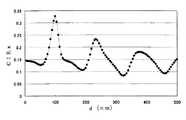
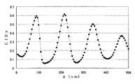
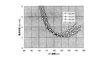
また図3は、青色副画素の有機EL素子の発光層内の発光位置と第2の反射面との間の光学距離dを変化させたときの発光効率η(cd/A)を示す説明図である。図4は、青色副画素の有機EL素子の発光層内の発光位置と第2の反射面との間の光学距離dを変化させたときの色度(CIEx)を示す説明図である。図5は、青色副画素の有機EL素子の発光層内の発光位置と第2の反射面との間の光学距離dを変化させたときの色度(CIEy)を示す説明図である。図6は、250cd/m2の白色表示時の青色副画素の有機発光素子の必要電流密度(mA/cm2)を示す説明図である。FIG. 3 is an explanatory diagram showing luminous efficiency η (cd / A) when the optical distance d between the light emitting position in the light emitting layer of the organic EL element of the blue subpixel and the second reflecting surface is changed. It is. FIG. 4 is an explanatory diagram showing chromaticity (CIEx) when the optical distance d between the light emitting position in the light emitting layer of the organic EL element of the blue subpixel and the second reflecting surface is changed. FIG. 5 is an explanatory diagram showing chromaticity (CIEy) when the optical distance d between the light emitting position in the light emitting layer of the organic EL element of the blue subpixel and the second reflecting surface is changed. FIG. 6 is an explanatory diagram showing the necessary current density (mA / cm2 ) of the organic light-emitting element of the blue sub-pixel when displaying white at 250 cd / m2 .
図3に示すように、発光効率ηの曲線は、その振幅が減衰しながら、ある値に収束していくことが分かる。以下、この値を輝度収束値と呼ぶ。これは、発光材料のフォトルミネッセンス(以下、PLと略す)が、ある半値幅をもつことに由来する。つまり、半値幅=ゼロであり、PLがインパルス関数(ディラックのデルタ関数)のようであれば、有機EL素子の発光効率ηの曲線が減衰することはない。しかし、実際には自然界にそのようなPLをもつ発光材料は見つかっておらず、有機EL素子から取り出される光の主なスペクトルのピークと、それに隣接するスペクトルが干渉し合い、互いに弱め合う。したがって、発光効率ηの曲線の高次の極値ほど、その絶対値が小さい。 As shown in FIG. 3, it can be seen that the curve of the luminous efficiency η converges to a certain value while the amplitude is attenuated. Hereinafter, this value is referred to as a luminance convergence value. This is because the photoluminescence of the light emitting material (hereinafter abbreviated as PL) has a certain half width. That is, if the half-value width is zero and PL is like an impulse function (Dirac delta function), the curve of the luminous efficiency η of the organic EL element will not be attenuated. However, in fact, no light emitting material having such a PL in nature has been found, and the main spectrum peak of light extracted from the organic EL element interferes with the spectrum adjacent to it and weakens each other. Therefore, the absolute value of the higher-order extreme value of the luminous efficiency η curve is smaller.
また、図4及び図5の色度(CIEx,CIEy)曲線についても、同様に色度の振幅が減衰しながらある値に収束していくことが分かる。 In addition, it can be seen that the chromaticity (CIEx, CIEy) curves in FIGS. 4 and 5 also converge to a certain value while the amplitude of chromaticity is attenuated.
さらに、図6は、有機EL素子の発光層内の発光位置と第2の反射面との間の光学距離Dを振って、それぞれ作製された有機EL素子の発光効率と色度の値を上記LB/ηBの式に入力し、当該する有機EL素子の必要電流を計算したものである。即ち、図6はRとGの色度で仮固定し、青色画素の有機EL素子の光学距離を横軸として、LB/ηBの式をプロットしたものである。図6の有機EL素子の必要電流も、発光効率の曲線の影響を受けて、その振幅が減衰しながら、ある値に収束していくのが分かる。なお、本発明において、必要電流あるいは消費電力が最小になる点とは、この減衰曲線のn次の極小値すべてを指す。Furthermore, FIG. 6 shows the values of the luminous efficiency and chromaticity of the organic EL element produced by varying the optical distance D between the light emitting position in the light emitting layer of the organic EL element and the second reflecting surface. This is input to the formula LB / ηB and the required current of the organic EL element concerned is calculated. That is, FIG. 6 is a graph in which the formula of LB / ηB is plotted with the horizontal axis representing the optical distance of the organic EL element of the blue pixel, temporarily fixed at the chromaticities of R and G. It can be seen that the required current of the organic EL element of FIG. 6 also converges to a certain value while the amplitude is attenuated due to the influence of the luminous efficiency curve. In the present invention, the point where the required current or power consumption is minimized refers to all the n-th order minimum values of this attenuation curve.
この減衰曲線のn次の極小値においては、膜厚の変動(ばらつき)があったとしても、必要電流の変化が緩やかであるため、パネルの消費電力が安定している。また、本発明で開示される極小値とは、±10%程度のばらつきを許容する。これは、±10%のばらつきがあったとしても、消費電力は十分に小さく、またパネルの消費電力は比較的安定しているからである。なお、±10%は、極小値を示す光学距離からのずれを表すものである。 In the nth-order minimum value of this attenuation curve, even if there is a variation (variation) in the film thickness, the required current changes gently, so that the power consumption of the panel is stable. Further, the local minimum value disclosed in the present invention allows a variation of about ± 10%. This is because even if there is a variation of ± 10%, the power consumption is sufficiently small and the power consumption of the panel is relatively stable. Here, ± 10% represents a deviation from the optical distance indicating the minimum value.
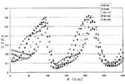
また、本実施形態の有機EL素子は、第1の反射面と第2の反射面との間の光学距離が最適化されていることが望ましい。図7は、有機EL素子の発光層内の発光位置と第2の反射面との間の光学距離dを変化させたときの発光効率η(cd/A)を示す説明図である。図8は、有機EL素子の発光層内の発光位置と第2の反射面との間の光学距離dを変化させたときの色度(CIEx値)を示す説明図である。図9は、有機EL素子の発光層内の発光位置と第2の反射面との間の光学距離dを変化させたときの色度(CIEy値)を示す説明図である。図10は、有機EL素子の発光層内の発光位置と第2の反射面との間の光学距離dを変化させたときの必要電流を示す説明図である。なお、図7から図10において、Dは発光層内の発光位置と第1の反射層との間の発光距離である。 In the organic EL element of the present embodiment, it is desirable that the optical distance between the first reflecting surface and the second reflecting surface is optimized. FIG. 7 is an explanatory diagram showing light emission efficiency η (cd / A) when the optical distance d between the light emission position in the light emitting layer of the organic EL element and the second reflecting surface is changed. FIG. 8 is an explanatory diagram showing chromaticity (CIEx value) when the optical distance d between the light emitting position in the light emitting layer of the organic EL element and the second reflecting surface is changed. FIG. 9 is an explanatory diagram showing chromaticity (CIEy value) when the optical distance d between the light emitting position in the light emitting layer of the organic EL element and the second reflecting surface is changed. FIG. 10 is an explanatory diagram showing the required current when the optical distance d between the light emitting position in the light emitting layer of the organic EL element and the second reflecting surface is changed. In FIG. 7 to FIG. 10, D is the light emitting distance between the light emitting position in the light emitting layer and the first reflective layer.
第1の反射面と第2の反射面との間の光学距離は、発光層内の発光位置と第1の反射面の光学距離と、発光層内の発光位置と第2反射面との光学距離の和で表わされる。したがって、図7から図10では、発光層内の発光位置と第2の反射面との間の光学距離d、及び第1の反射面と第2の反射面との間の光学距離Dの双方を最適化している。 The optical distance between the first reflecting surface and the second reflecting surface is the optical distance between the light emitting position in the light emitting layer and the first reflecting surface, and the optical distance between the light emitting position in the light emitting layer and the second reflecting surface. Expressed as the sum of distances. Therefore, in FIGS. 7 to 10, both the optical distance d between the light emitting position in the light emitting layer and the second reflecting surface and the optical distance D between the first reflecting surface and the second reflecting surface are both. Is optimized.
図7に示すように、発光効率ηの曲線は、その振幅が減衰しながら、輝度収束値に収束していくことが分かる。また、図8及び図9の色度(CIEx,CIEy)曲線についても、同様に色度の振幅が減衰しながら色度収束値に収束していくことが分かる。 As shown in FIG. 7, it can be seen that the curve of the luminous efficiency η converges to the luminance convergence value while the amplitude is attenuated. Further, it can be seen that the chromaticity (CIEx, CIEy) curves of FIGS. 8 and 9 also converge to the chromaticity convergence value while the amplitude of the chromaticity is similarly attenuated.
さらに、図10の250cd/m2の白色表示時の必要電流の曲線も、その振幅を減衰させながら、ある一定の値に収束している。前述のとおり、本発明において、必要電流あるいは消費電力が最小になる点とは、この減衰曲線のn次の極小値すべてを指す。また、この必要電流あるいは消費電力が最小になる点近傍では、膜厚の変動(ばらつき)があったとしても、必要電流の変化が緩やかであるため、表示装置(パネル)の消費電力が安定している。Further, the required current curve at the time of white display of 250 cd / m2 in FIG. 10 also converges to a certain value while the amplitude is attenuated. As described above, in the present invention, the point where the required current or power consumption is minimized refers to all the n-th order minimum values of this attenuation curve. Also, in the vicinity of the point where the required current or power consumption becomes minimum, even if there is a variation (variation) in the film thickness, the change in the required current is gentle, so the power consumption of the display device (panel) is stable. ing.
このように、有機EL素子の発光層内の発光位置と第2の反射面との間の光学距離dだけではなく、第1の反射面と第2の反射面との間の光学距離Dも最適化することにより、さらに有機EL素子の必要電流を小さくすることが可能であることが分かる。 Thus, not only the optical distance d between the light emitting position in the light emitting layer of the organic EL element and the second reflecting surface, but also the optical distance D between the first reflecting surface and the second reflecting surface. It can be seen that the required current of the organic EL element can be further reduced by optimization.
また、RGBごとに干渉を合わせるため、例えば、金属マスクなどを用いて、有機化合物層の膜厚(光学距離)を変えることが考えられる。その際、膜厚を調整する層として、電気抵抗の低い有機化合物材料を用いることが望ましい。電圧が低くなるほど、有機EL表示装置の消費電力が小さくなるからである。また、膜厚を調整する層として、該当する有機EL素子の発光色を透過させる有機化合物材料を用いることが望ましい。透過率が高いほど、有機EL素子の輝度が上がるからである。 Moreover, in order to match interference for every RGB, it is possible to change the film thickness (optical distance) of an organic compound layer using a metal mask etc., for example. At that time, it is desirable to use an organic compound material having low electric resistance as a layer for adjusting the film thickness. This is because the lower the voltage, the lower the power consumption of the organic EL display device. Moreover, it is desirable to use the organic compound material which permeate | transmits the luminescent color of an applicable organic EL element as a layer which adjusts a film thickness. This is because the higher the transmittance, the higher the luminance of the organic EL element.
さらに、本発明において、有機EL表示装置の白色の色度は自由に設定することが可能であり、例えば、NTSC色度座標の(Wx,Wy)=(0.310,0.316)が考えられる。また例えば、D65標準色度(Wx,Wy)=(0.31271,0.32902)が考えられる。 Furthermore, in the present invention, the white chromaticity of the organic EL display device can be freely set. For example, the NTSC chromaticity coordinate (Wx, Wy) = (0.310, 0.316) is considered. It is done. For example, D65 standard chromaticity (Wx, Wy) = (0.31271, 0.32902) can be considered.
以上で示した方法は、有機EL表示装置が白色表示する際に、ある1色の副画素の素子の必要電流を最小にする方法であるが、前提として、他の副画素の色度が仮固定されている必要がある。そのため、有機EL表示装置全体に流れる電流量を最小にするために、本発明で開示する方法を各色の副画素に繰り返し適用し、順次帰納法で各色の副画素の光学膜厚を最適化する方法が考えられる。以下にその方法を詳しく説明する。 The method described above is a method for minimizing the necessary current of the element of a certain subpixel when the organic EL display device performs white display. However, as a premise, the chromaticity of other subpixels is assumed to be temporary. Must be fixed. Therefore, in order to minimize the amount of current flowing through the entire organic EL display device, the method disclosed in the present invention is repeatedly applied to the subpixels of each color, and the optical film thickness of the subpixels of each color is optimized by the sequential induction method. A method is conceivable. The method will be described in detail below.
まず、3色のうち2色の色度を仮固定し、本発明において、それ以外の1色の素子の光学膜厚を最適化する。ここでは、例えば、RとGの色度を仮固定し、Bの素子の光学膜厚を最適化するものとする。次に、最適化された素子の色度は一意に決まるため、それ以外の2色のうち1色の色度を仮固定する。 First, the chromaticity of two of the three colors is temporarily fixed, and in the present invention, the optical film thickness of the other one color element is optimized. Here, for example, the chromaticities of R and G are temporarily fixed, and the optical film thickness of the element B is optimized. Next, since the chromaticity of the optimized element is uniquely determined, the chromaticity of one of the other two colors is temporarily fixed.
ここでは、例えば、Rの色度を仮固定し、既に最適化されているBの色度と合わせて、Gの素子の光学膜厚を最適化するものとする。次に、最適化された素子の色度は一意に決まるため、それ以外の1色、すなわちRの光学膜厚を最適化する。さらに、もう1度、RとGの色度を固定化し、Bの光学膜厚を再度最適化する。これを繰り返すと、RGBそれぞれの副画素の光学膜厚がそれぞれの最適値に収束していくため、有機EL表示装置全体に流れる電流量を最小にすることが可能である。 Here, for example, the chromaticity of R is temporarily fixed, and the optical film thickness of the G element is optimized together with the already optimized B chromaticity. Next, since the chromaticity of the optimized element is uniquely determined, the optical film thickness of the other color, that is, R, is optimized. Furthermore, the chromaticities of R and G are fixed once again, and the optical film thickness of B is optimized again. If this process is repeated, the optical film thicknesses of the RGB sub-pixels converge to their optimum values, so that the amount of current flowing through the entire organic EL display device can be minimized.
なお、TFTの配線のレイアウトの都合から電源電圧をRGB共通にしている場合は、有機EL表示装置全体に流れる電流量を最小にしたとき、表示装置全体の消費電力も最小となる。しかし、電源電圧をRGB別々にしている場合は、そうはならない。このとき表示装置全体の消費電力Pは、P=VR×IR+VG×IG+VB×IBの式で表わされる。If the power supply voltage is common to RGB for the convenience of the layout of TFT wiring, when the amount of current flowing through the entire organic EL display device is minimized, the power consumption of the entire display device is also minimized. However, this is not the case when the power supply voltages are RGB separately. Power consumption P of the entire display device at this time is represented by the equationP = V R × I R + V G × I G + V B × I B.
ここで、VR:R画素にかかる電圧、VG:G画素にかかる電圧、VB:B画素にかかる電圧である。また、IR:R画素に流れる電流の合計、IG:G画素に流れる電流の合計、IB:B画素に流れる電流の合計であり、IR=S×iR、IG=S×iG、IB=S×iB;Sは発光面積、iは電流密度である。Here, VR is a voltage applied to the R pixel, VG is a voltage applied to the G pixel, and VB is a voltage applied to the B pixel. IR : total current flowing through the R pixel, IG : total current flowing through the G pixel, IB : total current flowing through the B pixel, IR = S × iR , IG = S × iG , IB = S × iB ; S is a light emitting area, and i is a current density.
有機EL表示装置全体の消費電力Pを最小にするためには、各副画素に印加される電圧も加味した上で、上記方法を適用する必要がある。 In order to minimize the power consumption P of the entire organic EL display device, it is necessary to apply the above method in consideration of the voltage applied to each subpixel.
以上のように、有機EL素子の発光層内の発光位置と第2の反射面との間の光学距離、及び第1の反射面と第2の反射面との間の光学距離のそれぞれを最適化し、有機EL素子の必要電流および有機EL表示装置の消費電力を最小にしている。 As described above, the optical distance between the light emitting position in the light emitting layer of the organic EL element and the second reflecting surface and the optical distance between the first reflecting surface and the second reflecting surface are optimum. The required current of the organic EL element and the power consumption of the organic EL display device are minimized.
さらに、本発明において、有機EL素子の発光層内の発光位置と第2の反射面との間の光学距離に対する必要電流曲線の2次の極小値を用いることが望ましい。有機EL素子の発光層内の発光位置と第2の反射面との間の光学距離が短い場合は、陽極−陰極間にリーク電流が発生し、ダークスポットや輝点の原因となるからである。2次の極小値を用いることによって、有機EL素子の発光層内の発光位置と第2の反射面との間の光学距離を、ある程度厚くすることになるので、多少の異物が存在してもリークしない有機EL素子を作製することが可能となる。有機EL素子のリークを防止することにより、有機EL表示装置の製造の歩留まりを向上させることができる。 Furthermore, in the present invention, it is desirable to use the second-order minimum value of the required current curve with respect to the optical distance between the light emitting position in the light emitting layer of the organic EL element and the second reflecting surface. This is because when the optical distance between the light emitting position in the light emitting layer of the organic EL element and the second reflecting surface is short, a leak current is generated between the anode and the cathode, causing dark spots and bright spots. . By using the secondary minimum value, the optical distance between the light emitting position in the light emitting layer of the organic EL element and the second reflecting surface is increased to some extent, so even if some foreign matter exists. An organic EL element that does not leak can be manufactured. By preventing the leakage of the organic EL element, the production yield of the organic EL display device can be improved.
以上、本発明の好適な実施形態を説明したが、これは本発明の説明のための例示であり、本発明の要旨を逸脱しない範囲で、上記実施形態とは異なる種々の態様で実施することができる。 The preferred embodiment of the present invention has been described above. However, this is merely an example for explaining the present invention, and various embodiments different from the above-described embodiment may be implemented without departing from the gist of the present invention. Can do.
例えば、上記実施形態ではトップエミッション型の有機EL素子を複数備えた表示装置の例について説明したが、基板側から光を取り出すボトムエミッション型の有機EL素子を複数備えた表示装置であっても適用可能である。 For example, in the above embodiment, an example of a display device including a plurality of top emission type organic EL elements has been described. However, the present invention is also applicable to a display device including a plurality of bottom emission type organic EL elements that extract light from the substrate side. Is possible.
以下に、実施例を示して、本発明に係る有機EL表示装置をより詳細に説明するが、本発明はこれらの実施例に限定されない。 The organic EL display device according to the present invention will be described in more detail below with reference to examples, but the present invention is not limited to these examples.
〔実施例1〕
実施例1の有機EL表示装置は、各画素がトップエミッション型の有機EL素子からなり、陽極が基板側に位置し、陰極が光取り出し側に位置する層構成である。また、実施例1の有機EL表示装置は、RGBの3色を副画素として有する。[Example 1]
The organic EL display device of Example 1 has a layer configuration in which each pixel is formed of a top emission type organic EL element, an anode is located on the substrate side, and a cathode is located on the light extraction side. The organic EL display device of Example 1 has three colors of RGB as subpixels.
実施例1は、第1の反射面とRGBの各有機化合物層の光取り出し側の端面までの光学距離は共通であり、有機EL素子の発光層内の発光位置と第2の反射面との間の光学距離のみRGBごとに異なる構成である。 In Example 1, the optical distance between the first reflecting surface and the end surface on the light extraction side of each of the RGB organic compound layers is the same, and the light emitting position in the light emitting layer of the organic EL element and the second reflecting surface are the same. Only the optical distance between them is different for each RGB.
再び図1を参照して、実施例1の有機EL表示装置の作製方法について説明する。図1に示すように、まず、TFTが形成された基板1上に、コンタクトホールを有する平坦化膜を形成した。なお、図1において、TFT、平坦化膜及びコンタクトホールは図示していない。 With reference to FIG. 1 again, a manufacturing method of the organic EL display device of Example 1 will be described. As shown in FIG. 1, first, a planarizing film having contact holes was formed on a
次に、真空装置中でスパッタ法によって、平坦膜上にAg合金膜を100nm形成した上に、同じくスパッタ法によって酸化インジウム錫(ITO)膜を10nm積層し、これらをパターニングすることにより陽極2とした。なお、図1中には、Ag合金膜と酸化インジウム錫(ITO)膜を合わせて陽極2として表している。陽極2はコンタクトホールを介してTFTに接続されている。また、Ag合金膜は陽極であるとともに、第2の反射面の役割を果たす。 Next, an Ag alloy film having a thickness of 100 nm is formed on the flat film by sputtering in a vacuum apparatus, and then an indium tin oxide (ITO) film having a thickness of 10 nm is formed by sputtering. did. In FIG. 1, the Ag alloy film and the indium tin oxide (ITO) film are collectively shown as the
次に、陽極2上に形成した絶縁層に対して、フォトリソグラフィ技術を用いて不図示の素子分離膜を作製した。この素子分離膜は、画素および副画素を分離し、TFTによって独立に駆動させるために設けられる。 Next, with respect to the insulating layer formed on the
次に、基板の前処理について説明する。基板の前処理は、まずアルバック社製の真空装置中で、基板が100℃になるようにして5分間加熱した。続いて、装置中に乾燥空気を導入し、UVを基板に照射することにより、オゾン洗浄を行なった。さらに、装置中を真空に戻したのち、10分間加熱した。 Next, substrate pretreatment will be described. For the pretreatment of the substrate, first, the substrate was heated for 5 minutes in a vacuum apparatus manufactured by ULVAC so that the substrate was at 100 ° C. Then, ozone cleaning was performed by introducing dry air into the apparatus and irradiating the substrate with UV. Further, the inside of the apparatus was returned to a vacuum and then heated for 10 minutes.
前処理が終了したのち、正孔輸送層(ホール輸送層)3を形成する。正孔輸送層3としては、下記構造式HT1の正孔輸送材料を用いた。正孔輸送層の膜厚は、金属マスクを用いてRGBごとに変える。正孔輸送層の膜厚については後述する。 After the pretreatment is completed, a hole transport layer (hole transport layer) 3 is formed. As the
続いて、B画素に対してのみ、電子ブロック層4を形成する。本実施例では、R及びG画素に対しては、電子ブロック層4は形成しない。したがって、B画素の正孔輸送層を成膜後、基板から金属マスクを取り外さず、電子ブロック層4を成膜するチャンバへと移動させた。ここで、下記構造式HT2の電子ブロック材料を10nmの膜厚となるように成膜した。 Subsequently, the electronic block layer 4 is formed only for the B pixel. In this embodiment, the electron block layer 4 is not formed for the R and G pixels. Therefore, after forming the hole transport layer of the B pixel, the metal mask was not removed from the substrate and moved to the chamber in which the electron block layer 4 was formed. Here, an electron block material having the following structural formula HT2 was formed to a thickness of 10 nm.
次に、発光層の形成について詳しく説明する。まず、Gの発光層7の形成について説明する。電子ブロック層4を形成後、一旦、金属マスクを基板から取り外した。そして、金属マスクを再度、基板にアライメントしてRB画素を覆い、G画素のみ開口している状態にして、Gの発光層を蒸着するためのチャンバへと移動させた。下記構造式GD8の緑色発光ドーパント(10vol%)と、下記構造式GD12のアシストドーパント(30vol%)と、下記構造式GH3の発光層ホスト材料の共蒸着膜を45nmの膜厚で成膜してGの発光層7を形成した。Gの発光層内の発光位置は、基板から近い方に分布している。 Next, the formation of the light emitting layer will be described in detail. First, the formation of the G
次に、Rの発光層6の形成について説明する。Gの発光層7を形成後、一旦、金属マスクを基板から取り外した。そして、金属マスクを再度、基板にアライメントしてG,B画素を覆い、R画素のみ開口している状態にして、Rの発光層を蒸着するためのチャンバへと移動させた。下記構造式RD10の赤色発光ドーパント(3vol%)と、下記構造式RD12のアシストドーパント(10vol%)と、下記構造式RH4の発光層ホスト材料の共蒸着膜を50nmの膜厚で成膜してRの発光層6を形成した。Rの発光層内の発光位置は、基板から近い方に分布している。 Next, formation of the R
最後に、Bの発光層8の形成について説明する。Rの発光層6を形成後、一旦、金属マスクを基板から取り外した。そして、金属マスクを再度、基板にアライメントしてG,R画素を覆い、B画素のみ開口している状態にして、Bの発光層を蒸着するためのチャンバへと移動させた。下記構造式BD12の青色発光ドーパント(5vol%)と、下記構造式BH14の発光層ホスト材料の共蒸着膜を35nmの膜厚で成膜してBの発光層8を形成した。Bの発光層内の発光位置は、基板から遠い方に分布している。以上のように発光層を形成した。 Finally, formation of the B
以下の層については、RGB共通である。発光層成膜後、金属マスクを基板から取り外した。正孔ブロック層を蒸着するためのチャンバへと移動させ、下記構造式HB1で示される有機化合物を10nmの膜厚で成膜して正孔ブロック層9を形成した。 The following layers are common to RGB. After forming the light emitting layer, the metal mask was removed from the substrate. It moved to the chamber for vapor-depositing a hole block layer, and the organic compound shown by the following structural formula HB1 was formed into a film with a film thickness of 10 nm, and the hole block layer 9 was formed.
次に、電子輸送層を蒸着するためのチャンバへと移動させ、下記構造式ET25で示されるフェナントロリン化合物を10nmの膜厚で成膜して電子輸送層10を形成した。 Next, it moved to the chamber for vapor-depositing an electron carrying layer, the phenanthroline compound shown by following structural formula ET25 was formed into a film with a film thickness of 10 nm, and the
次に、電子輸送層10を形成後、電子注入層11を形成する。基板を電子注入層を蒸着するためのチャンバへと移動させた。そして、上記構造式ET25で示されるフェナントロリン化合物と炭酸セシウムを、セシウムの濃度が23wt%となるように蒸着レートを調整して、共蒸着膜の厚さが60nmになるまで成膜し、電子注入層11とした。 Next, after the
次に、電子注入層11上に陰極12を形成する。陰極12は、Agとインジウム亜鉛酸化物(IZO)を、この順に積層してなり、スパッタ法を用いて、Agを12nm、IZOを60nm形成した。AgとIZOの界面は第1の反射面となる。 Next, the
最後に、基板をN2雰囲気中に移動させ、基板1の周縁部に紫外線硬化樹脂を塗布し、この樹脂上にガラス基板を貼り合わせた状態で、紫外線を照射して硬化する。この際、画素部に紫外線が当たらないようにマスクする。Finally, the substrate is moved into an N2 atmosphere, an ultraviolet curable resin is applied to the peripheral edge of the
赤色副画素の正孔輸送層の膜厚は220nm、緑色副画素の正孔輸送層の膜厚は167nmとした。本実施例においては赤色副画素の色度はCIE色度座標系において(0.670,0.330)であった。また、緑色副画素の色度はCIE色度座標系において(0.240,0.698)であった。 The film thickness of the hole transport layer of the red subpixel was 220 nm, and the film thickness of the hole transport layer of the green subpixel was 167 nm. In this embodiment, the chromaticity of the red sub-pixel is (0.670, 0.330) in the CIE chromaticity coordinate system. The chromaticity of the green subpixel was (0.240, 0.698) in the CIE chromaticity coordinate system.
以下に、白色6500Kを表示させる際に、必要な消費電力を最小にすることを考える。図11及び図12を参照し、青色に関して、有機化合物層内の発光位置と第2の反射面までの光路長を変化させるため正孔輸送層(HTL)膜厚を振った時の特性変化を説明する。図11は、正孔輸送層(HTL)膜厚に対する電流効率及びCIEyの色度を示す説明図である。図11より、CIEyの極値を狙う場合には、正孔輸送層(HTL)=115nmとなり、電流効率の最大値を狙うには、正孔輸送層(HTL)=160nmとなる。なお、正孔輸送層(HTL)が150nmよりも厚い領域では、色再現範囲に白色6500Kが入らないため、白色を表示できなくなる。 In the following, it is considered to minimize power consumption necessary for displaying white 6500K. 11 and 12, with respect to blue, the change in characteristics when the hole transport layer (HTL) film thickness is changed to change the light emission position in the organic compound layer and the optical path length to the second reflecting surface. explain. FIG. 11 is an explanatory diagram showing current efficiency and CIEy chromaticity with respect to the hole transport layer (HTL) film thickness. From FIG. 11, when aiming at the extreme value of CIEy, the hole transport layer (HTL) = 115 nm, and when aiming at the maximum current efficiency, the hole transport layer (HTL) = 160 nm. In the region where the hole transport layer (HTL) is thicker than 150 nm, white color cannot be displayed because white 6500K does not enter the color reproduction range.
また、図12は、正孔輸送層(HTL)膜厚に対する白色を出す際の青色副画素の必要電流密度及び消費電力を示す説明図である。図12から分かる通り、青色副画素の必要電流密度と消費電力の間には正の相関があり、必要電流密度が最小となる。正孔輸送層(HTL)=135nmは消費電力の最小値近傍となっている。 FIG. 12 is an explanatory diagram showing the required current density and power consumption of the blue subpixel when white is produced with respect to the hole transport layer (HTL) film thickness. As can be seen from FIG. 12, there is a positive correlation between the required current density of the blue subpixel and the power consumption, and the required current density is minimized. The hole transport layer (HTL) = 135 nm is close to the minimum value of power consumption.
実施例1は青色副画素の必要電流密度を最小とする構成とし、CIEyの極値をとる構成を比較例1、電流効率を最大にする構成を比較例2として消費電力の比較を行ったものが表1である。表1から分かる通り、青色副画素の必要電流密度を最小とした本実施例は最も消費電力が低い。 Example 1 is a configuration in which the required current density of the blue sub-pixel is minimized, a configuration that takes the extreme value of CIEy is a comparative example 1, and a configuration that maximizes the current efficiency is a comparative example 2 in which power consumption is compared. Is Table 1. As can be seen from Table 1, the power consumption is lowest in this embodiment in which the required current density of the blue subpixel is minimized.
また、この実施例1の色度に基づいて、RとGの有機化合物層内の発光位置と第2の反射面までの光路長を計算する。すると、実施例1のRとGの有機化合物層内の発光位置と第2の反射面までの光路長がそれぞれRとGの素子の必要電流が極小を示す光路長の±10%以内の範囲に入っていた。 Further, based on the chromaticity of Example 1, the light emission position in the organic compound layer of R and G and the optical path length to the second reflecting surface are calculated. Then, the light emission position in the organic compound layer of R and G in Example 1 and the optical path length to the second reflecting surface are within ± 10% of the optical path length at which the required currents of the R and G elements are minimum, respectively. I was in.
〔実施例2〕
実施例2の有機EL表示装置はRGBの発光副画素からなり、RGの素子構成は実施例1と同一である。実施例2では、Bの素子構成について、有機化合物層内の発光位置と第2の反射面との光学距離のみならず、有機化合物層内の発光位置と第1の反射面との光学距離も最適化する。すなわち、第1の反射面から第2の反射面までの光学距離も最適化している。[Example 2]
The organic EL display device of Example 2 includes RGB light emitting subpixels, and the element configuration of RG is the same as that of Example 1. In Example 2, not only the optical distance between the light emitting position in the organic compound layer and the second reflecting surface but also the optical distance between the light emitting position in the organic compound layer and the first reflecting surface in the element configuration of B Optimize. That is, the optical distance from the first reflecting surface to the second reflecting surface is also optimized.
R,GとBの有機化合物層内の発光位置と第1の反射面との光学距離を変えるために、金属マスクを用いて電子輸送層を塗り分ける。 In order to change the optical distance between the light emitting position in the organic compound layer of R, G and B and the first reflecting surface, the electron transport layer is applied separately using a metal mask.
有機化合物層内の発光位置と第1の反射面との間の光学距離を振るために電子注入層(EIL)膜厚を、第2の反射面から有機化合物層内の発光位置の間の光学距離を変化させるために、正孔輸送層(HTL)膜厚を振った。このときの青色副画素における必要電流密度の変化を図13に示す。図13は、正孔輸送層(HTL)膜厚を変化させたときの電子注入層(EIL)の膜厚に対する電流密度(mA/cm2)の変化である。図13から分かる通り、電子注入層(EIL)が薄いほど電流密度は低くなっている。In order to change the optical distance between the light emitting position in the organic compound layer and the first reflecting surface, the electron injection layer (EIL) film thickness is set to be the same as the optical distance between the second reflecting surface and the light emitting position in the organic compound layer. In order to change the distance, the hole transport layer (HTL) film thickness was varied. The change in required current density in the blue subpixel at this time is shown in FIG. FIG. 13 shows changes in current density (mA / cm2 ) with respect to the thickness of the electron injection layer (EIL) when the thickness of the hole transport layer (HTL) is changed. As can be seen from FIG. 13, the thinner the electron injection layer (EIL), the lower the current density.
また、このときの消費電力の変化を図14に示す。図14は、正孔輸送層(HTL)膜厚を変化させたときの電子注入層(EIL)の膜厚に対する消費電力(mW)の変化である。図14から分かる通り、必要電流密度の変化と同様にして電子注入層(EIL)が薄いほど消費電力は低くなっている。電子注入層(EIL)が薄いほど、発光点から光取り出し電極間までの光路長が青色の干渉長に合致していくためである。 Further, FIG. 14 shows changes in power consumption at this time. FIG. 14 shows changes in power consumption (mW) with respect to the thickness of the electron injection layer (EIL) when the thickness of the hole transport layer (HTL) is changed. As can be seen from FIG. 14, as the required current density changes, the thinner the electron injection layer (EIL), the lower the power consumption. This is because as the electron injection layer (EIL) is thinner, the optical path length from the light emitting point to between the light extraction electrodes matches the blue interference length.
青色副画素における必要電流密度の最小値をとる特性は次の通りであった。すなわち、電子注入層(EIL)の膜厚が15nm、正孔輸送層(HTL)の膜厚が135nmで、CIEx(0.130)、CIEy(0.085)、発光効率が6.1(cd/A)及び消費電力が297(mW)であった。 The characteristic that takes the minimum value of the required current density in the blue sub-pixel was as follows. That is, the electron injection layer (EIL) has a film thickness of 15 nm, the hole transport layer (HTL) has a film thickness of 135 nm, CIEx (0.130), CIEy (0.085), and a light emission efficiency of 6.1 (cd). / A) and power consumption was 297 (mW).
2 第2の電極(陽極(金属反射膜)、3 ホール輸送層、4 電子ブロック層、6,7,8 発光層、9 正孔ブロック層、10 電子輸送層、11 電子注入層、12 第1の電極(陰極)2 Second electrode (anode (metal reflective film), 3 hole transport layer, 4 electron block layer, 6, 7, 8 light emitting layer, 9 hole block layer, 10 electron transport layer, 11 electron injection layer, 12 1st Electrode (cathode)
Claims (7)
Translated fromJapanese前記RGBの3色のうち少なくとも1色の有機EL素子の発光層内での発光位置と前記第2の反射面との間の光学距離は、白色表示する際に、前記光学距離を変化させたときの必要電流密度の曲線におけるn次の極小値から±10%となる値であることを特徴とする有機EL表示装置。Between the first electrode on the light extraction side and the second electrode facing the first electrode, a plurality of organic EL elements of RGB three-color subpixels having an organic compound layer including a light emitting layer are provided, The organic EL element includes a first reflective surface that is closer to the first electrode than the organic compound layer and a second reflective surface that is closer to the second electrode than the organic compound layer. In an organic EL display device having a resonance structure for resonating light generated in the light emitting layer,
The optical distance between the light emitting position in the light emitting layer of the organic EL element of at least one of the three colors of RGB and the second reflecting surface was changed when displaying white. An organic EL display device having avalue that is ± 10% from an nth-order minimum value in a curve of required current density.
前記RGBの3色の有機EL素子の発光層内での発光位置と前記第2の反射面との間の光学距離は、白色表示する際に、前記光学距離を変化させたときの必要電流密度の曲線におけるn次の極小値から±10%となる値であることを特徴とする有機EL表示装置。Between the first electrode on the light extraction side and the second electrode facing the first electrode, a plurality of organic EL elements of RGB three-color subpixels having an organic compound layer including a light emitting layer are provided, The organic EL element includes a first reflective surface that is closer to the first electrode than the organic compound layer and a second reflective surface that is closer to the second electrode than the organic compound layer. In an organic EL display device having a resonance structure for resonating light generated in the light emitting layer,
The optical distance between the light emitting position in the light emitting layer of the RGB three-color organic EL element and the second reflecting surface is the required current density when the optical distance is changed when displaying white. An organic EL display device having avalue of ± 10% from the n-th minimum value in the curve.
Priority Applications (4)
| Application Number | Priority Date | Filing Date | Title |
|---|---|---|---|
| JP2010163790AJP5676949B2 (en) | 2010-07-21 | 2010-07-21 | Organic EL display device |
| US13/185,717US8618559B2 (en) | 2010-07-21 | 2011-07-19 | Organic electroluminescent display |
| CN201110205236.5ACN102347450B (en) | 2010-07-21 | 2011-07-21 | Organic electroluminescent display device |
| US14/069,177US9136309B2 (en) | 2010-07-21 | 2013-10-31 | Organic electroluminescent display |
Applications Claiming Priority (1)
| Application Number | Priority Date | Filing Date | Title |
|---|---|---|---|
| JP2010163790AJP5676949B2 (en) | 2010-07-21 | 2010-07-21 | Organic EL display device |
Publications (3)
| Publication Number | Publication Date |
|---|---|
| JP2012028064A JP2012028064A (en) | 2012-02-09 |
| JP2012028064A5 JP2012028064A5 (en) | 2013-09-05 |
| JP5676949B2true JP5676949B2 (en) | 2015-02-25 |
Family
ID=45492840
Family Applications (1)
| Application Number | Title | Priority Date | Filing Date |
|---|---|---|---|
| JP2010163790AActiveJP5676949B2 (en) | 2010-07-21 | 2010-07-21 | Organic EL display device |
Country Status (3)
| Country | Link |
|---|---|
| US (2) | US8618559B2 (en) |
| JP (1) | JP5676949B2 (en) |
| CN (1) | CN102347450B (en) |
Families Citing this family (11)
| Publication number | Priority date | Publication date | Assignee | Title |
|---|---|---|---|---|
| US20120138874A1 (en) | 2010-12-02 | 2012-06-07 | Intematix Corporation | Solid-state light emitting devices and signage with photoluminescence wavelength conversion and photoluminescent compositions therefor |
| US8994056B2 (en)* | 2012-07-13 | 2015-03-31 | Intematix Corporation | LED-based large area display |
| KR101429725B1 (en) | 2012-10-31 | 2014-08-12 | 엘지디스플레이 주식회사 | Organic Light Emitting Display Device and fabricating method of the same |
| JPWO2014087462A1 (en)* | 2012-12-03 | 2017-01-05 | 株式会社日立製作所 | ORGANIC ELECTROLUMINESCENT LIGHT EMITTING DEVICE, ORGANIC ELECTROLUMINESCENT ELEMENT USED FOR THE SAME, AND LIGHT EXTRACTION SHEET USED FOR THE SAME |
| KR20150006605A (en)* | 2013-07-09 | 2015-01-19 | 삼성디스플레이 주식회사 | Organic light emitting display device and method of manufacturing an organic light emitting display device |
| US9978812B2 (en)* | 2014-01-14 | 2018-05-22 | Sharp Kabushiki Kaisha | Organic electroluminescent display panel |
| US9318670B2 (en) | 2014-05-21 | 2016-04-19 | Intematix Corporation | Materials for photoluminescence wavelength converted solid-state light emitting devices and arrangements |
| JP6888943B2 (en)* | 2016-11-17 | 2021-06-18 | 株式会社ジャパンディスプレイ | Organic electroluminescence display device |
| CN111869325B (en)* | 2018-03-16 | 2023-06-16 | 富士胶片株式会社 | Electroluminescence display device |
| KR102597673B1 (en)* | 2018-05-16 | 2023-11-02 | 삼성디스플레이 주식회사 | Display device |
| US11877489B2 (en) | 2020-09-29 | 2024-01-16 | Universal Display Corporation | High color gamut OLED displays |
Family Cites Families (38)
| Publication number | Priority date | Publication date | Assignee | Title |
|---|---|---|---|---|
| JP4001692B2 (en)* | 1999-02-18 | 2007-10-31 | パイオニア株式会社 | Organic electroluminescence device and manufacturing method thereof |
| TW463528B (en) | 1999-04-05 | 2001-11-11 | Idemitsu Kosan Co | Organic electroluminescence element and their preparation |
| JP4136185B2 (en) | 1999-05-12 | 2008-08-20 | パイオニア株式会社 | Organic electroluminescent multicolor display and method for manufacturing the same |
| JP4094919B2 (en)* | 2002-07-18 | 2008-06-04 | 東北パイオニア株式会社 | Organic light emitting display |
| JP2005150043A (en)* | 2003-11-19 | 2005-06-09 | Fuji Electric Holdings Co Ltd | Organic EL light emitting device |
| CN1918949A (en)* | 2004-03-05 | 2007-02-21 | 出光兴产株式会社 | Organic electroluminescent element and display device |
| JP2006295104A (en)* | 2004-07-23 | 2006-10-26 | Semiconductor Energy Lab Co Ltd | LIGHT EMITTING ELEMENT AND LIGHT EMITTING DEVICE USING THE SAME |
| JP4823629B2 (en)* | 2004-09-24 | 2011-11-24 | 株式会社半導体エネルギー研究所 | Light emitting device |
| JP4384107B2 (en)* | 2004-10-25 | 2009-12-16 | キヤノン株式会社 | Organic light emitting device array |
| KR100683711B1 (en)* | 2004-11-22 | 2007-02-20 | 삼성에스디아이 주식회사 | Organic light emitting display device |
| JP2005101008A (en)* | 2004-12-24 | 2005-04-14 | Sanyo Electric Co Ltd | Organic electroluminescent element and its manufacturing method |
| JP2006179780A (en)* | 2004-12-24 | 2006-07-06 | Canon Inc | Organic light emitting device and display panel |
| US7948171B2 (en)* | 2005-02-18 | 2011-05-24 | Semiconductor Energy Laboratory Co., Ltd. | Light emitting device |
| US7564181B2 (en)* | 2005-04-08 | 2009-07-21 | Eastman Kodak Company | Performance enhancement layer for OLED devices |
| JP4789706B2 (en)* | 2005-06-08 | 2011-10-12 | 株式会社半導体エネルギー研究所 | Light-emitting element, light-emitting device, electronic device |
| WO2006134519A2 (en)* | 2005-06-14 | 2006-12-21 | Koninklijke Philips Electronics N.V. | Multi view display device |
| JP2007005173A (en)* | 2005-06-24 | 2007-01-11 | Toshiba Matsushita Display Technology Co Ltd | Display device |
| JP2007110090A (en)* | 2005-09-13 | 2007-04-26 | Sony Corp | GaN-based semiconductor light emitting device, light emitting device, image display device, planar light source device, and liquid crystal display device assembly |
| JP5207645B2 (en)* | 2006-03-29 | 2013-06-12 | キヤノン株式会社 | Multicolor organic light emitting device |
| JP5241128B2 (en)* | 2006-04-26 | 2013-07-17 | キヤノン株式会社 | Multicolor display device |
| JP4898560B2 (en)* | 2006-06-23 | 2012-03-14 | キヤノン株式会社 | Organic light emitting device |
| JP2008135373A (en)* | 2006-10-24 | 2008-06-12 | Canon Inc | Organic light emitting device and method for manufacturing the same |
| JP2008210665A (en)* | 2007-02-27 | 2008-09-11 | Canon Inc | ORGANIC LIGHT EMITTING ELEMENT AND DISPLAY DEVICE USING THE SAME |
| JP2008225179A (en)* | 2007-03-14 | 2008-09-25 | Sony Corp | Display device, driving method of the display device, and electronic apparatus |
| US8227978B2 (en)* | 2007-10-10 | 2012-07-24 | Samsung Electronics Co., Ltd. | White organic light emitting device and color display apparatus employing the same |
| KR101434361B1 (en)* | 2007-10-16 | 2014-08-26 | 삼성디스플레이 주식회사 | White organic light emitting device and color display apparatus employing the same |
| KR101434362B1 (en)* | 2007-10-17 | 2014-08-26 | 삼성디스플레이 주식회사 | Organic electroluminescent device and color display device using the same |
| JP4450051B2 (en)* | 2007-11-13 | 2010-04-14 | ソニー株式会社 | Display device |
| JP5219493B2 (en)* | 2007-11-14 | 2013-06-26 | キヤノン株式会社 | Light emitting element and light emitting device using the same |
| JP2009231274A (en)* | 2008-02-27 | 2009-10-08 | Canon Inc | Organic light-emitting element, and display apparatus |
| JP2009289592A (en)* | 2008-05-29 | 2009-12-10 | Canon Inc | Display |
| JP2010080423A (en)* | 2008-08-29 | 2010-04-08 | Fujifilm Corp | Color display device and its manufacturing method |
| JP2010146738A (en)* | 2008-12-16 | 2010-07-01 | Seiko Epson Corp | Light-emitting device and method of manufacturing the same as well as electronic equipment |
| JP5127814B2 (en)* | 2008-12-19 | 2013-01-23 | キヤノン株式会社 | ORGANIC LIGHT EMITTING ELEMENT AND LIGHT EMITTING DEVICE AND DISPLAY DEVICE USING THE SAME |
| JP5164825B2 (en)* | 2008-12-19 | 2013-03-21 | キヤノン株式会社 | Organic light emitting device |
| JPWO2011046166A1 (en)* | 2009-10-14 | 2013-03-07 | コニカミノルタホールディングス株式会社 | ORGANIC ELECTROLUMINESCENCE ELEMENT AND LIGHTING DEVICE USING THE SAME |
| JPWO2011055440A1 (en)* | 2009-11-05 | 2013-03-21 | キヤノン株式会社 | Display device |
| US8686448B2 (en)* | 2011-05-27 | 2014-04-01 | Seiko Epson Corporation | Light emitting device, electronic apparatus, and manufacturing method of light emitting device |
- 2010
- 2010-07-21JPJP2010163790Apatent/JP5676949B2/enactiveActive
- 2011
- 2011-07-19USUS13/185,717patent/US8618559B2/ennot_activeExpired - Fee Related
- 2011-07-21CNCN201110205236.5Apatent/CN102347450B/enactiveActive
- 2013
- 2013-10-31USUS14/069,177patent/US9136309B2/enactiveActive
Also Published As
| Publication number | Publication date |
|---|---|
| CN102347450B (en) | 2015-02-25 |
| US20140054576A1 (en) | 2014-02-27 |
| US8618559B2 (en) | 2013-12-31 |
| US9136309B2 (en) | 2015-09-15 |
| US20120018712A1 (en) | 2012-01-26 |
| CN102347450A (en) | 2012-02-08 |
| JP2012028064A (en) | 2012-02-09 |
Similar Documents
| Publication | Publication Date | Title |
|---|---|---|
| JP5676949B2 (en) | Organic EL display device | |
| US10229954B2 (en) | Organic light-emitting device and organic light-emitting display device using the same | |
| TWI500144B (en) | Organic light emitting display device and method of manufacturing same | |
| JP5008486B2 (en) | Display device | |
| US20120018749A1 (en) | Organic light emitting display apparatus and method for manufacturing the same | |
| US9076978B2 (en) | Organic light emitting diode device | |
| US9343510B2 (en) | Organic light emitting display device | |
| CN103779387B (en) | Oled display panel and display device | |
| CN113272990A (en) | Multi-mode microcavity OLEDs with multiple blue light emitting layers | |
| WO2006109493A1 (en) | Luminescent element, light emitting deivce comprising said luminescent element, and process for producing the same | |
| JP2011018451A (en) | Light-emitting display apparatus | |
| JP2010080738A (en) | Organic el display device and method of manufacturing the same | |
| KR102000292B1 (en) | Organic light emitting display device and method for manufacturing thereof | |
| KR101074808B1 (en) | Blue light emitting element and Organic light emitting display adopting the element | |
| KR20140077523A (en) | Organic light emitting diode display device | |
| WO2017043243A1 (en) | Organic electroluminescence device, organic electroluminescence device manufacturing method, lighting device and display device | |
| KR20200013901A (en) | Display device | |
| WO2020232911A1 (en) | Electroluminescent display device | |
| CN107275501A (en) | Organic light-emitting structure, display device and mobile terminal | |
| Cho et al. | Organic light-emitting diode structure for high color gamut in high-resolution microdisplay: Over 90% color gamut based on BT. 2020 | |
| KR20130046640A (en) | Organic electroluminescent diode and method of fabricating the same | |
| JP2012054091A (en) | Multicolor display device | |
| KR20150010384A (en) | Organic Light Emitting Device | |
| KR101849583B1 (en) | White organic light emitting display device | |
| KR102113609B1 (en) | Organic light emitting display and manufactucring method of the same |
Legal Events
| Date | Code | Title | Description |
|---|---|---|---|
| A521 | Request for written amendment filed | Free format text:JAPANESE INTERMEDIATE CODE: A523 Effective date:20130718 | |
| A621 | Written request for application examination | Free format text:JAPANESE INTERMEDIATE CODE: A621 Effective date:20130718 | |
| A977 | Report on retrieval | Free format text:JAPANESE INTERMEDIATE CODE: A971007 Effective date:20140225 | |
| A131 | Notification of reasons for refusal | Free format text:JAPANESE INTERMEDIATE CODE: A131 Effective date:20140304 | |
| A977 | Report on retrieval | Free format text:JAPANESE INTERMEDIATE CODE: A971007 Effective date:20140424 | |
| A521 | Request for written amendment filed | Free format text:JAPANESE INTERMEDIATE CODE: A523 Effective date:20140507 | |
| TRDD | Decision of grant or rejection written | ||
| A01 | Written decision to grant a patent or to grant a registration (utility model) | Free format text:JAPANESE INTERMEDIATE CODE: A01 Effective date:20141202 | |
| A61 | First payment of annual fees (during grant procedure) | Free format text:JAPANESE INTERMEDIATE CODE: A61 Effective date:20141226 | |
| R151 | Written notification of patent or utility model registration | Ref document number:5676949 Country of ref document:JP Free format text:JAPANESE INTERMEDIATE CODE: R151 |