JP5674613B2 - Control system, control method and program - Google Patents
Control system, control method and programDownload PDFInfo
- Publication number
- JP5674613B2 JP5674613B2JP2011207807AJP2011207807AJP5674613B2JP 5674613 B2JP5674613 B2JP 5674613B2JP 2011207807 AJP2011207807 AJP 2011207807AJP 2011207807 AJP2011207807 AJP 2011207807AJP 5674613 B2JP5674613 B2JP 5674613B2
- Authority
- JP
- Japan
- Prior art keywords
- data
- memory area
- storage device
- main storage
- memory
- Prior art date
- Legal status (The legal status is an assumption and is not a legal conclusion. Google has not performed a legal analysis and makes no representation as to the accuracy of the status listed.)
- Expired - Fee Related
Links
Images


Classifications
- G—PHYSICS
- G06—COMPUTING OR CALCULATING; COUNTING
- G06F—ELECTRIC DIGITAL DATA PROCESSING
- G06F12/00—Accessing, addressing or allocating within memory systems or architectures
- G06F12/02—Addressing or allocation; Relocation
- G06F12/08—Addressing or allocation; Relocation in hierarchically structured memory systems, e.g. virtual memory systems
- G06F12/0802—Addressing of a memory level in which the access to the desired data or data block requires associative addressing means, e.g. caches
- G06F12/0893—Caches characterised by their organisation or structure
- G—PHYSICS
- G06—COMPUTING OR CALCULATING; COUNTING
- G06F—ELECTRIC DIGITAL DATA PROCESSING
- G06F1/00—Details not covered by groups G06F3/00 - G06F13/00 and G06F21/00
- G06F1/26—Power supply means, e.g. regulation thereof
- G06F1/32—Means for saving power
- G06F1/3203—Power management, i.e. event-based initiation of a power-saving mode
- G06F1/3234—Power saving characterised by the action undertaken
- G06F1/325—Power saving in peripheral device
- G06F1/3275—Power saving in memory, e.g. RAM, cache
- G—PHYSICS
- G06—COMPUTING OR CALCULATING; COUNTING
- G06F—ELECTRIC DIGITAL DATA PROCESSING
- G06F1/00—Details not covered by groups G06F3/00 - G06F13/00 and G06F21/00
- G06F1/26—Power supply means, e.g. regulation thereof
- G06F1/32—Means for saving power
- G06F1/3203—Power management, i.e. event-based initiation of a power-saving mode
- G06F1/3234—Power saving characterised by the action undertaken
- G06F1/3287—Power saving characterised by the action undertaken by switching off individual functional units in the computer system
- G—PHYSICS
- G06—COMPUTING OR CALCULATING; COUNTING
- G06F—ELECTRIC DIGITAL DATA PROCESSING
- G06F12/00—Accessing, addressing or allocating within memory systems or architectures
- G06F12/02—Addressing or allocation; Relocation
- G06F12/08—Addressing or allocation; Relocation in hierarchically structured memory systems, e.g. virtual memory systems
- G06F12/0802—Addressing of a memory level in which the access to the desired data or data block requires associative addressing means, e.g. caches
- G06F12/0804—Addressing of a memory level in which the access to the desired data or data block requires associative addressing means, e.g. caches with main memory updating
- G—PHYSICS
- G06—COMPUTING OR CALCULATING; COUNTING
- G06F—ELECTRIC DIGITAL DATA PROCESSING
- G06F12/00—Accessing, addressing or allocating within memory systems or architectures
- G06F12/02—Addressing or allocation; Relocation
- G06F12/08—Addressing or allocation; Relocation in hierarchically structured memory systems, e.g. virtual memory systems
- G06F12/0802—Addressing of a memory level in which the access to the desired data or data block requires associative addressing means, e.g. caches
- G06F12/0864—Addressing of a memory level in which the access to the desired data or data block requires associative addressing means, e.g. caches using pseudo-associative means, e.g. set-associative or hashing
- G—PHYSICS
- G06—COMPUTING OR CALCULATING; COUNTING
- G06F—ELECTRIC DIGITAL DATA PROCESSING
- G06F2212/00—Indexing scheme relating to accessing, addressing or allocation within memory systems or architectures
- G06F2212/10—Providing a specific technical effect
- G06F2212/1028—Power efficiency
- Y—GENERAL TAGGING OF NEW TECHNOLOGICAL DEVELOPMENTS; GENERAL TAGGING OF CROSS-SECTIONAL TECHNOLOGIES SPANNING OVER SEVERAL SECTIONS OF THE IPC; TECHNICAL SUBJECTS COVERED BY FORMER USPC CROSS-REFERENCE ART COLLECTIONS [XRACs] AND DIGESTS
- Y02—TECHNOLOGIES OR APPLICATIONS FOR MITIGATION OR ADAPTATION AGAINST CLIMATE CHANGE
- Y02D—CLIMATE CHANGE MITIGATION TECHNOLOGIES IN INFORMATION AND COMMUNICATION TECHNOLOGIES [ICT], I.E. INFORMATION AND COMMUNICATION TECHNOLOGIES AIMING AT THE REDUCTION OF THEIR OWN ENERGY USE
- Y02D10/00—Energy efficient computing, e.g. low power processors, power management or thermal management
- Y—GENERAL TAGGING OF NEW TECHNOLOGICAL DEVELOPMENTS; GENERAL TAGGING OF CROSS-SECTIONAL TECHNOLOGIES SPANNING OVER SEVERAL SECTIONS OF THE IPC; TECHNICAL SUBJECTS COVERED BY FORMER USPC CROSS-REFERENCE ART COLLECTIONS [XRACs] AND DIGESTS
- Y02—TECHNOLOGIES OR APPLICATIONS FOR MITIGATION OR ADAPTATION AGAINST CLIMATE CHANGE
- Y02D—CLIMATE CHANGE MITIGATION TECHNOLOGIES IN INFORMATION AND COMMUNICATION TECHNOLOGIES [ICT], I.E. INFORMATION AND COMMUNICATION TECHNOLOGIES AIMING AT THE REDUCTION OF THEIR OWN ENERGY USE
- Y02D30/00—Reducing energy consumption in communication networks
- Y02D30/50—Reducing energy consumption in communication networks in wire-line communication networks, e.g. low power modes or reduced link rate
Landscapes
- Engineering & Computer Science (AREA)
- Theoretical Computer Science (AREA)
- General Engineering & Computer Science (AREA)
- Physics & Mathematics (AREA)
- General Physics & Mathematics (AREA)
- Computer Hardware Design (AREA)
- Computing Systems (AREA)
- Memory System Of A Hierarchy Structure (AREA)
Description
Translated fromJapanese本発明の実施形態は、制御システム、制御方法およびプログラムに関する。 Embodiments described herein relate generally to a control system, a control method, and a program.
近年、携帯電話、スレート型端末およびタブレット型端末などの情報機器などから、スーパーコンピュータなどの大規模システムに至る幅広い計算機システムにおいて、システムの省電力化が重要な課題となっている。省電力化の一つの方法として、電力を必要としている部分(ユニット)にだけ電力を供給するパワーゲーティング技術などが挙げられる。 In recent years, in a wide range of computer systems ranging from information devices such as mobile phones, slate terminals, and tablet terminals to large-scale systems such as supercomputers, system power saving has become an important issue. As one method of power saving, there is a power gating technique that supplies power only to a portion (unit) that needs power.
例えば計算機システムのプロセッサが何も処理を実行しないアイドル状態の場合、プロセッサの処理に用いられる複数のデータの一部が記憶されるキャッシュメモリに対する電力供給を停止することで、省電力化を図ることができる。ここで、キャッシュメモリは、RAMなどの揮発性のメモリで構成されるのが一般的であるため、キャッシュメモリに対する電力供給を停止した場合、キャッシュメモリに記憶されたデータも全て消えてしまう。このため、キャッシュメモリに対する電力供給を停止する場合は、キャッシュメモリに記憶されたデータのうち、書き換えられたデータ(主記憶装置に記憶された内容と一致していないデータ)を主記憶装置へ書き戻すライトバック処理を行う必要がある。 For example, when the processor of the computer system is in an idle state in which no processing is performed, power saving is achieved by stopping power supply to a cache memory in which a part of a plurality of data used for the processor processing is stored. Can do. Here, since the cache memory is generally composed of a volatile memory such as a RAM, when the power supply to the cache memory is stopped, all data stored in the cache memory is also erased. For this reason, when power supply to the cache memory is stopped, of the data stored in the cache memory, rewritten data (data that does not match the content stored in the main storage device) is written to the main storage device. It is necessary to perform write-back processing to return.
しかしながら、上述のライトバック処理によって発生する消費電力量が、キャッシュメモリに対する電力供給を停止しない場合の消費電力量よりも大きい場合も想定される。この場合にライトバック処理を行ってキャッシュメモリに対する電力供給を停止することは、消費電力量の低減に繋がらない。すなわち、アイドル状態の場合は無条件にライトバック処理を行ってキャッシュメモリに対する電力供給を停止する構成では、消費電力量を効率的に低減することが困難であるという問題がある。 However, a case where the power consumption generated by the above-described write-back process is larger than the power consumption when power supply to the cache memory is not stopped is also assumed. In this case, performing the write-back process to stop the power supply to the cache memory does not lead to a reduction in power consumption. That is, there is a problem that it is difficult to efficiently reduce the power consumption in the configuration in which the write back processing is unconditionally performed in the idle state to stop the power supply to the cache memory.
本発明が解決しようとする課題は、消費電力量を効率的に低減可能な制御システム、制御方法およびプログラムを提供することである。 The problem to be solved by the present invention is to provide a control system, a control method, and a program capable of efficiently reducing power consumption.
実施形態の制御システムは、処理装置と主記憶装置とキャッシュメモリと電源部とを備えた制御システムであって、検出部と推定部と判断部と制御部とを備える。検出部はアイドル状態を検出する。推定部はアイドル時間を推定する。判断部は、アイドル状態が検出された場合、主記憶装置への書き戻しが必要なデータの書き戻しを行ってキャッシュメモリに対する電力の供給を停止した場合の第1消費電力量が、当該データの書き戻しを行わずにアイドル時間にわたってキャッシュメモリに対する電力の供給を継続した場合の第2消費電力量よりも大きいか否かを判断する。制御部は、第1消費電力量が第2消費電力量よりも小さいと判断された場合は、キャッシュメモリに対する電力供給を停止させる一方、第1消費電力量が第2消費電力量よりも大きいと判断された場合は、キャッシュメモリに対する電力供給を継続させる。 The control system of the embodiment is a control system including a processing device, a main storage device, a cache memory, and a power supply unit, and includes a detection unit, an estimation unit, a determination unit, and a control unit. The detection unit detects an idle state. The estimation unit estimates idle time. When the determination unit detects an idle state, the first power consumption amount when the supply of power to the cache memory is stopped by writing back the data that needs to be written back to the main storage device is It is determined whether or not the power consumption is greater than the second power consumption when the supply of power to the cache memory is continued for the idle time without performing the write-back. When it is determined that the first power consumption is smaller than the second power consumption, the control unit stops power supply to the cache memory, while the first power consumption is larger than the second power consumption. If it is determined, the power supply to the cache memory is continued.
実施形態の制御方法は、処理装置と主記憶装置とキャッシュメモリと電源部とを備えた制御システムの制御方法であって、検出ステップと推定ステップと判断ステップと制御ステップとを備える。検出ステップではアイドル状態を検出する。推定ステップではアイドル時間を推定する。判断ステップでは、アイドル状態が検出された場合、主記憶装置への書き戻しが必要なデータの書き戻しを行ってキャッシュメモリに対する電力の供給を停止した場合の第1消費電力量が、当該データの書き戻しを行わずにアイドル時間にわたってキャッシュメモリに対する電力の供給を継続した場合の第2消費電力量よりも大きいか否かを判断する。制御ステップでは、第1消費電力量が第2消費電力量よりも小さいと判断された場合は、キャッシュメモリに対する電力供給を停止させる一方、第1消費電力量が第2消費電力量よりも大きいと判断された場合は、キャッシュメモリに対する電力供給を継続させる。 A control method according to an embodiment is a control method for a control system including a processing device, a main storage device, a cache memory, and a power supply unit, and includes a detection step, an estimation step, a determination step, and a control step. In the detection step, an idle state is detected. In the estimation step, idle time is estimated. In the determination step, when an idle state is detected, the first power consumption when the supply of power to the cache memory is stopped by writing back the data that needs to be written back to the main storage device is It is determined whether or not the power consumption is greater than the second power consumption when the supply of power to the cache memory is continued for the idle time without performing the write-back. In the control step, when it is determined that the first power consumption is smaller than the second power consumption, the power supply to the cache memory is stopped, while the first power consumption is larger than the second power consumption. If it is determined, the power supply to the cache memory is continued.
実施形態のプログラムは、処理装置と主記憶装置とキャッシュメモリと電源部とを備えたコンピュータに、検出ステップと推定ステップと判断ステップと制御ステップとを実行させるためのプログラムである。検出ステップではアイドル状態を検出する。推定ステップではアイドル時間を推定する。判断ステップでは、アイドル状態が検出された場合、主記憶装置への書き戻しが必要なデータの書き戻しを行ってキャッシュメモリに対する電力の供給を停止した場合の第1消費電力量が、当該データの書き戻しを行わずにアイドル時間にわたってキャッシュメモリに対する電力の供給を継続した場合の第2消費電力量よりも大きいか否かを判断する。制御ステップでは、第1消費電力量が第2消費電力量よりも小さいと判断された場合は、キャッシュメモリに対する電力供給を停止させる一方、第1消費電力量が第2消費電力量よりも大きいと判断された場合は、キャッシュメモリに対する電力供給を継続させる。 The program according to the embodiment is a program for causing a computer including a processing device, a main storage device, a cache memory, and a power supply unit to execute a detection step, an estimation step, a determination step, and a control step. In the detection step, an idle state is detected. In the estimation step, idle time is estimated. In the determination step, when an idle state is detected, the first power consumption when the supply of power to the cache memory is stopped by writing back the data that needs to be written back to the main storage device is It is determined whether or not the power consumption is greater than the second power consumption when the supply of power to the cache memory is continued for the idle time without performing the write-back. In the control step, when it is determined that the first power consumption is smaller than the second power consumption, the power supply to the cache memory is stopped, while the first power consumption is larger than the second power consumption. If it is determined, the power supply to the cache memory is continued.
以下、添付図面を参照しながら、本発明に係る制御システム、制御方法およびプログラムの実施の形態を詳細に説明する。 Hereinafter, embodiments of a control system, a control method, and a program according to the present invention will be described in detail with reference to the accompanying drawings.
(第1実施形態)
図1は、第1実施形態の制御システム100の構成例を示すブロック図である。図1に示すように、制御システム100は、処理装置10と、キャッシュメモリ20と、主記憶装置30と、電力を供給する電源部40とを含んで構成される。キャッシュメモリ20と主記憶装置30は、バス110を介して接続される。なお、ここでは詳細な図示は省略するが、本実施形態の制御システム100は、他にも、ROM、HDDやSSDなどの外部記憶装置、ディスプレイなどの表示装置、マウスやキーボードなどの入力装置、および、通信I/F装置などを備えており、通常のコンピュータを利用したハードウェア構成となっている。(First embodiment)
FIG. 1 is a block diagram illustrating a configuration example of a
処理装置10は、データを処理する。処理装置10は、各種の処理を実行し、制御システム100全体の動作を制御する。処理装置10は、例えばCPU(Central Processing Unit)などの制御装置で構成され得る。主記憶装置30は、処理装置10が実行する処理に用いられる複数のデータを記憶する。 The processing device 10 processes data. The processing device 10 executes various processes and controls the operation of the
キャッシュメモリ20は、主記憶装置30に記憶された複数のデータの一部を記憶する。キャッシュメモリ20は、例えばスタティックRAM(Random Access Memory)などの揮発性のメモリで構成され、電力の供給が停止すると記憶内容は消失する。図2は、キャッシュメモリ20の構成例を示すブロック図である。図2に示すように、キャッシュメモリ20は、有効ビット21、ダーティビット22、アドレス23を格納するタグメモリアレイ24と、キャッシュ対象のデータ(「キャッシュデータ」と呼ぶ)25を格納するデータメモリアレイ26と、ダーティビットカウンタ27とを有する。 The cache memory 20 stores a part of a plurality of data stored in the main storage device 30. The cache memory 20 is composed of a volatile memory such as a static RAM (Random Access Memory), for example, and the stored contents are lost when power supply is stopped. FIG. 2 is a block diagram illustrating a configuration example of the cache memory 20. As shown in FIG. 2, the cache memory 20 includes a
キャッシュメモリ20は、エントリ28単位でデータを格納し、各エントリ28は、有効ビット21、ダーティビット22、アドレス23およびキャッシュデータ25で構成される。 The cache memory 20 stores data in units of
有効ビット21は、対応するエントリ28のキャッシュデータ25が有効か否かを示す。図3の例では、対応するエントリ28のキャッシュデータ25が有効である場合、有効ビット21は「1」に設定され、キャッシュデータ25が無効である場合、有効ビット21は「0」に設定される。 The valid bit 21 indicates whether or not the
ダーティビット22は、対応するエントリ28のキャッシュデータ25が、主記憶装置30のうち当該エントリ28のアドレス23が示す位置に格納されたデータと一致しているか否かを示す。図3の例では、ダーティビット22は、対応するエントリ28のキャッシュデータ25が、主記憶装置30のうち当該エントリ28のアドレス23が示す位置に格納されたデータと一致していない場合は「1」に設定される。一方、対応するエントリ28のキャッシュデータ25が、主記憶装置30のうち当該エントリ28のアドレス23が示す位置に格納されたデータと一致している場合は、ダーティビット22は「0」に設定される。例えばデータの転送命令(ストア命令)が発行されて、あるエントリ28のキャッシュデータ25が書き換えられた場合、そのエントリ28のダーティビット22は「1」に設定される。見方を変えれば、ダーティビット22は、対応するエントリ28のキャッシュデータ25が、主記憶装置30への書き戻しが必要なデータであるか否かを示す情報であると捉えることもできる。 The
アドレス23は、主記憶装置30のうち、対応するエントリ28のキャッシュデータ25が格納されるべき位置を示す。 The address 23 indicates a position in the main storage device 30 where the
ダーティビットカウンタ27は、ダーティビット22が「1」に設定されたエントリ28の総数をカウントする。すなわち、ダーティビットカウンタ27は、キャッシュデータ25のうち、主記憶装置30への書き戻しが必要なキャッシュデータ25の総数をカウントする。 The dirty bit counter 27 counts the total number of
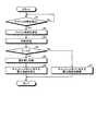
図3は、処理装置10が不図示のHDD等に格納されたプログラムを実行することにより実現される機能を示すブロック図である。つまりは、制御システム100の機能ブロック図であると捉えることもできる。図3に示すように、制御システム100の機能には、検出部51と推定部52と判断部53と判断部53と再開部55とが含まれる。なお、これらの機能のうちの少なくとも一部を個別の回路(ハードウェア)で実現することもできる。 FIG. 3 is a block diagram showing functions realized by the processing device 10 executing a program stored in an HDD (not shown) or the like. That is, it can also be understood as a functional block diagram of the
検出部51は、処理装置10が処理を実行していないアイドル状態であるか否かを検出する。推定部52は、アイドル状態が継続する時間を示すアイドル時間を推定する。推定部52によるアイドル時間の推定方法は任意である。例えばキーなどのデバイスの操作入力待ちにより処理装置10がアイドル状態となる場合を想定する。デバイスの操作入力は個人差があるものの、同じ人が入力するタイミングは大体同じであると考えられるので、過去の操作入力の履歴から操作入力が行われる間隔の平均値(平均間隔と呼ぶ)を求め、その求めた平均間隔から、前回の操作入力が行われてから経過した時間を引いた値をアイドル時間として推定することもできる。例えば過去3回の操作入力の間隔が、500ms,450ms,550msで、前回の操作入力が行われてから経過した時間が100msの場合、{(500+450+550)/3−100}×1000=400,000μsecをアイドル時間として推定することができる。 The
判断部53は、検出部51によりアイドル状態が検出された場合、キャッシュメモリ20に格納されたキャッシュデータ25のうち主記憶装置30への書き戻しが必要なキャッシュデータ25の書き戻しを行ってキャッシュメモリ20に対する電力の供給を停止した場合の第1消費電力量E1が、当該キャッシュデータ25の書き戻しを行わずに、推定部52で推定されたアイドル時間にわたってキャッシュメモリ20に対する電力の供給を継続した場合の第2消費電力量E2よりも小さいか否かを判断する。より具体的には、判断部53は、キャッシュメモリ20に格納されたキャッシュデータ25のうち主記憶装置30への書き戻しが必要なキャッシュデータ25の総数(ダーティビットカウンタ27のカウント値)と、推定部52で推定されたアイドル時間とを用いて、第1消費電力量E1が第2消費電力量E2よりも小さいか否かを判断する。さらに詳述すれば以下のとおりである。 When the
いま、書き戻しが行われる場合の平均電力量をPw、1つのキャッシュデータ25の書き戻しに必要な時間の平均値をTw1、書き戻しが必要なデータの総数をWB、キャッシュメモリ20に対する通電を停止して再度通電する際に発生するオーバヘッド分の消費電力量をCとすれば、第1消費電力量E1は式(1)で表される。
E1=Pw×(Tw1×WB)+C (1)Now, Pw is the average amount of power when writing back is performed, Tw1 is the average value of the time required to write back one
E1 = Pw × (Tw1 × WB) + C (1)
また、キャッシュメモリ20に対する電力供給が行われている場合の平均消費電力量をPo、推定部52で推定されたアイドル時間をTとすれば、第2消費電力量E2は式(2)で表される。
E2=Po×T (2)Further, when the average power consumption when power is supplied to the cache memory 20 is Po and the idle time estimated by the estimation unit 52 is T, the second power consumption E2 is expressed by Expression (2). Is done.
E2 = Po × T (2)
ここで、第1消費電力量E1が第2消費電力量E2よりも小さい場合は、式(3)が成立する。
WB<(Po/Pw/Tw1)×T−(C/Pw/Tw1) (3)
式(3)において、(Po/Pw/Tw1)および(C/Pw/Tw1)の各々の値は、制御システム100の構成に応じて決定される。したがって、(Po/Pw/Tw1)を定数Aに置き換え、(C/Pw/Tw1)を、定数Bに置き換えることで、式(3)を式(4)に変形できる。
WB<A×T−B (4)
すなわち、主記憶装置30への書き戻しが必要なキャッシュデータ25の総数WBと、アイドル時間Tとが分かれば、式(4)が成立するか否かを判断することで、第1消費電力量E1が第2消費電力量E2よりも小さいか否かを判断することができる。Here, when the first power consumption amount E1 is smaller than the second power consumption amount E2, Expression (3) is established.
WB <(Po / Pw / Tw1) × T- (C / Pw / Tw1) (3)
In Equation (3), each value of (Po / Pw / Tw1) and (C / Pw / Tw1) is determined according to the configuration of the
WB <A × T-B (4)
That is, if the total number WB of the
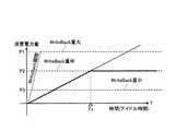
例えば図4において、第1の所定数のキャッシュデータ25の書き戻しを行う場合の消費電力量(第1消費電力量E1)をP1、第1の所定数よりも小さい第2の所定数のキャッシュデータ25の書き戻しを行う場合の消費電力量をP2、第2の所定数よりも小さい第3の所定数のキャッシュデータの書き戻しを行う場合の消費電力量をP3と表記する。いま、推定部52で推定されたアイドル時間TがTxであって、キャッシュデータ25の書き戻しを行わずにキャッシュメモリ20に対する電力供給を継続した場合の消費電力量(第2消費電力量E2)はP2に等しいとする。この場合、主記憶装置30への書き戻しが必要なキャッシュデータ25の総数WB(ダーティビットカウンタ27のカウント値)が第2の所定数よりも少なければ、第1消費電力量E1は第2消費電力量E2よりも小さくなる。一方、主記憶装置30への書き戻しが必要なキャッシュデータ25の総数WBが第2の所定数よりも多ければ、第1消費電力量E1は第2消費電力量E2よりも大きくなる。 For example, in FIG. 4, when the first predetermined number of
再び図3に戻って説明を続ける。判断部53により第1消費電力量E1が第2消費電力量E2よりも小さいと判断された場合、制御部54は、キャッシュデータ25の書き戻しを行ってキャッシュメモリ20に対する電源部40からの電力供給を停止させる。一方、判断部53により第1消費電力量E1が第2消費電力量E2よりも大きいと判断された場合、制御部54は、キャッシュデータ25の書き戻しを行わずにキャッシュメモリ20に対する電源部40からの電力供給を継続させる。 Returning to FIG. 3 again, the description will be continued. When the
再開部55は、キャッシュメモリ20に対する電力の供給が停止されている状態において、復帰要因を受け付けた場合に、キャッシュメモリ20に対する電力の供給を再開するように電源部40を制御する。復帰要因の種類は任意であり、例えば割り込み処理が復帰要因であってもよい。この場合、再開部55は、キャッシュメモリ20に対する電力の供給が停止されている状態において、割り込み処理を受け付けた場合に、キャッシュメモリ20に対する電力の供給を再開するように電源部40を制御する。 The resuming unit 55 controls the power supply unit 40 to resume the power supply to the cache memory 20 when a return factor is received in a state where the power supply to the cache memory 20 is stopped. The type of return factor is arbitrary. For example, interrupt processing may be a return factor. In this case, the resume unit 55 controls the power supply unit 40 to resume the supply of power to the cache memory 20 when an interrupt process is accepted in a state where the supply of power to the cache memory 20 is stopped.
図5は、制御システム100が実行する電源制御処理の一例を示すフローチャートである。この電源制御処理は、処理装置10が所定のソフトウェアプログラムを実行することにより実現される。図5に示すように、検出部51によりアイドル状態が検出された場合(ステップS1の結果:YES)、推定部52はアイドル時間を推定する(ステップS2)。 FIG. 5 is a flowchart illustrating an example of the power supply control process executed by the
次に、判断部53は、第1消費電力量E1が第2消費電力量E2よりも小さいか否かを判断する判断処理を行う(ステップS3)。本実施形態では、判断部53は、ダーティビットカウンタ27のカウント値を取得することで、主記憶装置30への書き戻しが必要なキャッシュデータ25の総数WBを特定する。そして、判断部53は、特定したキャッシュデータ25の総数WBと、ステップS2で推定されたアイドル時間Tとを用いて、上述の式(4)が成立するか否かを判断する。上述の式(4)が成立する場合は、第1消費電力量E1が第2消費電力量E2よりも小さいと判断する一方、上述の式(4)が成立しない場合は、第1消費電力量E1が第2消費電力量E2よりも大きいと判断する。 Next, the
例えば、上述の式(4)において、定数Aが1/100、定数Bが100、ステップS2で推定されたアイドル時間Tが400,00μsec、主記憶装置30への書き戻しが必要なキャッシュデータ25の総数(ダーティビットカウンタ27のカウント値)WBが200である場合を想定する。この場合、A×T−B=390となり、主記憶装置30への書き戻しが必要なキャッシュデータ25の総数WB(=200)を上回るので、式(4)は成立しない。したがって、判断部53は、第1消費電力量E1が第2消費電力量E2よりも大きいと判断する。 For example, in the above equation (4), the constant A is 1/100, the constant B is 100, the idle time T estimated in step S2 is 400,00 μsec, and the
判断部53により第1消費電力量E1が第2消費電力量E2よりも小さいと判断された場合(ステップS4の結果:YES)、制御部54は、ダーティビットが「1」に設定されたエントリ28のキャッシュデータ25を、主記憶装置30のうち当該エントリ28のアドレス23が示す位置に書き込む書き戻し処理を実行する(ステップS5)。書き戻し処理の後、制御部54は、キャッシュメモリ20に対する電力供給を停止するように電源部40を制御する(ステップS6)。 When the
一方、判断部53により第1消費電力量E1が第2消費電力量E2よりも大きいと判断された場合(ステップS4の結果:NO)、制御部54は、キャッシュメモリ20に対する電力供給を継続するように電源部40を制御する(ステップS7)。以上が電源制御処理の内容である。 On the other hand, when the
図6は、キャッシュメモリ20に対する電力供給を再開する再開処理の一例を示すフローチャートである。この再開処理は、処理装置10が所定のソフトウェアプログラムを実行することにより実現される。図6に示すように、復帰要因を受け付けた場合(ステップS11の結果:YES)、再開部55は、キャッシュメモリ20に対する電力の供給を再開するように電源部40を制御する(ステップS12)。 FIG. 6 is a flowchart illustrating an example of a restart process for restarting power supply to the cache memory 20. This resumption process is realized by the processing device 10 executing a predetermined software program. As illustrated in FIG. 6, when a return factor is received (result of step S11: YES), the restarting unit 55 controls the power supply unit 40 to restart the supply of power to the cache memory 20 (step S12).
以上に説明したように、本実施形態では、第1消費電力量E1が第2消費電力量E2よりも小さいと判断された場合は、キャッシュデータ25の書き戻しを行ってキャッシュメモリ20に対する電源部40からの電力供給を停止させる一方、第1消費電力量E1が第2消費電力量E2よりも大きいと判断された場合は、キャッシュデータ25の書き戻しを行わずにキャッシュメモリ20に対する電力供給を継続するので、第1消費電力量E1と第2消費電力量E2との関係を考慮せずに、アイドル状態が検出された場合は無条件にキャッシュデータ25の書き戻しを行う構成に比べて、消費電力量を効率的に低減することが可能になる。 As described above, in the present embodiment, when it is determined that the first power consumption amount E1 is smaller than the second power consumption amount E2, the
(第2実施形態)
次に、第2実施形態について説明する。第2実施形態のキャッシュメモリ200は、データが格納されるメモリ領域(「バンク」)が、複数のウェイごとに割り当てられたセットアソシアティブ方式のキャッシュメモリであり、キャッシュメモリ200に対する電源部40からの電力供給は、各ウェイに対応するメモリ領域ごとに行われる点で第1実施形態と相違する。以下、第1実施形態と相違する部分を中心に説明し、第1実施形態と共通する部分については、同一の符号を付して適宜に説明を省略する。(Second Embodiment)
Next, a second embodiment will be described. The cache memory 200 of the second embodiment is a set associative cache memory in which a memory area (“bank”) in which data is stored is assigned to each of a plurality of ways. The power supply is different from the first embodiment in that power is supplied for each memory area corresponding to each way. The following description will focus on parts that are different from the first embodiment, and parts that are the same as those in the first embodiment will be given the same reference numerals and description thereof will be omitted as appropriate.
図7は、第2実施形態のキャッシュメモリ200の構成例を示す図である。一例として、第2実施形態のキャッシュメモリ200は、4ウェイセットアソシアティブ方式のキャッシュメモリである。図7の例では、キャッシュメモリ200には、4つのウェイ(ウェイ0〜ウェイ3)の各々に割り当てられるメモリ領域が設けられる。ウェイ0に割り当てられるメモリ領域は、ウェイ0に対応するタグメモリアレイ240と、ウェイ0に対応するデータメモリアレイ260とを含む。ウェイ1に割り当てられるメモリ領域は、ウェイ1に対応するタグメモリアレイ241と、ウェイ1に対応するデータメモリアレイ261とを含む。ウェイ2に割り当てられるメモリ領域は、ウェイ2に対応するタグメモリアレイ242と、ウェイ2に対応するデータメモリアレイ262とを含む。ウェイ3に割り当てられるメモリ領域は、ウェイ3に対応するタグメモリアレイ243と、ウェイ3に対応するデータメモリアレイ263とを含む。キャッシュメモリ200は、エントリ28単位でデータを格納し、各エントリ28は、各ウェイに対応する有効ビット21、ダーティビット22、アドレス23およびキャッシュデータ25で構成される。なお、各エントリ28のデータは、ウェイ間で入れ替えることもできる。 FIG. 7 is a diagram illustrating a configuration example of the cache memory 200 according to the second embodiment. As an example, the cache memory 200 of the second embodiment is a 4-way set associative cache memory. In the example of FIG. 7, the cache memory 200 is provided with a memory area allocated to each of four ways (
また、キャッシュメモリ200が有するダーティビットカウンタ270は、ダーティビット22が「1」に設定されたエントリ28の総数をウェイごとにカウントする。 The dirty bit counter 270 included in the cache memory 200 counts the total number of
図8は、第2実施形態の制御システム300の機能ブロック図である。図8に示すように、制御システム300の機能には、入替部56がさらに含まれる点で第1実施形態と相違する。入替部56は、同じエントリ28におけるデータを2つのウェイ間で入れ替える処理(スワップ処理)を行う。この詳細な内容については後述する。また、第2実施形態の判断部530は、各ウェイに対応するメモリ領域ごとに、第1消費電力量E1が第2消費電力量E2よりも小さいか否かを判断する。すなわち、判断部530は、メモリ領域ごとに、ダーティビットが「1」に設定されたエントリ28の総数WBを特定する。そして、その特定した総数WBと、推定部52で推定されたアイドル時間Tとを用いて、上述の式(4)が成立するか否かの判断をメモリ領域ごとに行う。 FIG. 8 is a functional block diagram of the
さらに、第2実施形態の制御部540は、第1消費電力量E1が第2消費電力量E2よりも小さいと判断されたメモリ領域については、当該メモリ領域に格納されたキャッシュデータ25のうち、対応するダーティビット22が「1」に設定されたキャッシュデータ25の書き戻しを行って当該メモリ領域に対する電源部40からの電力供給を停止させる。一方、第1消費電力量E1が第2消費電力量E2よりも大きいと判断されたメモリ領域については、当該メモリ領域に格納されたキャッシュデータ25のうち、対応するダーティビット22が「1」に設定されたキャッシュデータ25の書き戻しを行わずに当該メモリ領域に対する電源部40からの電力供給を継続させる。 Furthermore, the
図9は、あるウェイiの第x番目のエントリ28(所定のエントリ)に対してダーティビット22を「1」に書き換えることが要求された場合(例えばストア命令が発行された場合)に、他のウェイj(i≠j)の第x番目のエントリ28に格納されたデータと入れ替える第1スワップ処理の一例を示すフローチャートである。 FIG. 9 shows another example when it is requested to rewrite the
図9に示すように、まず入替部56は、スワップ対象のウェイjを示す番号jを「0」に初期化する(ステップS21)。次に、入替部56は、番号jが、ダーティビット22の書き換えを要求されたウェイiを示す番号iよりも小さいか否かを判定する(ステップS22)。番号jが番号iよりも小さいと判定した場合(ステップS22の結果:YES)、入替部56は、番号jが示すウェイjの第x番目のエントリ28のダーティビット22が「0」であるか否かを判定する(ステップS23)。一方、番号jが番号iよりも大きいと判定した場合(ステップS22の結果:NO)、処理は後述のステップS26に移行する。 As shown in FIG. 9, first, the
ステップS23において、ウェイjの第x番目のエントリ28のダーティビット22が「0」ではないと判定した場合(ステップS23の結果:NO)、入替部56は、スワップ対象のウェイを示す番号jの値を1だけカウントアップし(ステップS24)、前述のステップS22からの処理を繰り返す。一方、ウェイjの第x番目のエントリ28のダーティビット22が「0」であると判定した場合(ステップS23の結果:YES)、入替部56は、ウェイiの第x番目のエントリ28に格納されたデータと、ウェイjの第x番目のエントリ28に格納されたデータとを入れ替える(ステップS25)。そして、入替部56は、ウェイjの第x番目のエントリ28に対応するダーティビット22を「1」に設定する(ステップS26)。 If it is determined in step S23 that the
図10は、あるウェイiの第x番目のエントリ28(所定のエントリ)に対してダーティビット22を「0」に書き換えることが要求された場合(例えば書き戻しを行う場合)に、他のウェイjの第x番目のエントリ28に格納されたデータと入れ替える第2スワップ処理の一例を示すフローチャートである。 FIG. 10 shows another way when the x-th entry 28 (predetermined entry) of a certain way i is requested to rewrite the
図10に示すように、まず入替部56は、ウェイ数(この例では「4」)から1を差し引いた値を、スワップ対象のウェイを示す番号jとして設定する(ステップS31)。次に、入替部56は、番号jが、ダーティビット22の書き換えを要求されたウェイiを示す番号iよりも大きいか否かを判定する(ステップS32)。番号jが番号iよりも大きいと判定した場合(ステップS32の結果:YES)、入替部56は、ウェイjの第x番目のエントリ28のダーティビット22が「1」であるか否かを判定する(ステップS33)。一方、番号jが番号iよりも小さいと判定した場合(ステップS32の結果:NO)、処理は後述のステップS36に移行する。 As shown in FIG. 10, the
ステップS33において、ウェイjの第x番目のエントリ28のダーティビット22が「1」ではないと判定した場合(ステップS33の結果:NO)、入替部56は、スワップ対象のウェイを示す番号jの値を1だけカウントダウンし(ステップS34)、前述のステップS32からの処理を繰り返す。一方、ウェイjの第x番目のエントリ28のダーティビット22が「1」であると判定した場合(ステップS33の結果:YES)、入替部56は、ウェイiの第x番目のエントリ28に格納されたデータと、ウェイjの第x番目のエントリ28に格納されたデータとを入れ替える(ステップS35)。そして、入替部56は、ウェイjの第x番目のエントリ28に対応するダーティビット22を「0」に設定する(ステップS36)。 If it is determined in step S33 that the
以上に説明したように、本実施形態では、主記憶装置30への書き戻しが必要なデータ(ダーティビット22が「1」に設定されたキャッシュデータ25)は、番号が小さいウェイに対応するメモリ領域に集約されるので、アイドル状態においては、番号が大きいウェイに対応するメモリ領域に対する電力供給が優先的に停止される。 As described above, in the present embodiment, data that needs to be written back to the main storage device 30 (
例えばウェイ0のダーティビット22のカウント値が800、ウェイ1のダーティビット22のカウント値が500、ウェイ2のダーティビット22のカウント値が200、ウェイ3のダーティビット22のカウント値が100、推定部52で推定されたアイドル時間Tが400,000μsec、上述の式(4)における定数Aが1/100、定数Bが100の場合を想定する。この場合、上述の式(4)において、A×T−B=390となるので、主記憶装置30への書き戻しが必要なキャッシュデータ25の総数WBが390未満であれば、第1消費電力量E1は第2消費電力量E2よりも小さいと判断される。したがって、ウェイ0およびウェイ1の各々に対応するメモリ領域については、キャッシュデータ25の書き戻しが行われずに電源部40からの電力供給が継続される。一方、ウェイ2およびウェイ3の各々に対応するメモリ領域については、キャッシュデータ25の書き戻しが行われて電源部40からの電力供給が停止される。 For example, the count value of the
なお、本実施形態では、4ウェイセットアソシアティブ方式のキャッシュメモリを例に挙げて説明したが、これに限らず、ウェイ数は任意である。要するに、キャッシュメモリは、第1ウェイに割り当てられた第1メモリ領域と、第2ウェイに割り当てられた第2メモリ領域とを少なくとも備えていればよい。 In the present embodiment, a 4-way set associative cache memory has been described as an example. However, the present invention is not limited to this, and the number of ways is arbitrary. In short, the cache memory only needs to include at least a first memory area assigned to the first way and a second memory area assigned to the second way.
また、本実施形態とは反対に、主記憶装置30への書き戻しが必要なキャッシュデータ25(ダーティビット22が「1」に設定されたキャッシュデータ25)が、番号が大きいウェイに対応するメモリ領域に集約される構成であってもよい。要するに、入替部56は、第1メモリ領域の第1エントリに格納されたデータが、主記憶装置30への書き戻しが必要なデータであって、第2メモリ領域の第1エントリに格納されたデータが、主記憶装置30への書き戻しが必要なデータではない場合、第1メモリ領域の第1エントリに格納されたデータと、第2メモリ領域の第2エントリに格納されたデータとを入れ替える機能を有するものであればよい。これにより、主記憶装置30への書き戻しが必要なデータを第2メモリ領域に集約することが可能になる。なお、第2メモリ領域に対応する第2ウェイを示す番号と第1ウェイを示す番号との大小関係は任意に変更可能である。 Contrary to this embodiment, the cache data 25 (
さらに、本実施形態では、ダーティビット22が「1」に設定されたキャッシュデータ25が、番号が小さいウェイに対応するメモリ領域に集約される構成を説明したが、例えば有効ビット21が「1」に設定されたキャッシュデータ25が、番号が小さいウェイ(または番号が大きいウェイ)に対応するメモリ領域に集約される構成とすることもできる。 Furthermore, in the present embodiment, the configuration has been described in which the
以上、本発明の実施形態を説明したが、上述の各実施形態は、例として提示したものであり、発明の範囲を限定することは意図していない。これら新規な実施形態は、その他の様々な形態で実施されることが可能であり、発明の要旨を逸脱しない範囲で、種々の省略、置き換え、変更を行うことができる。これら実施形態やその変形は、発明の範囲や要旨に含まれるとともに、特許請求の範囲に記載された発明とその均等の範囲に含まれる。 As mentioned above, although embodiment of this invention was described, each above-mentioned embodiment was shown as an example and is not intending limiting the range of invention. These novel embodiments can be implemented in various other forms, and various omissions, replacements, and changes can be made without departing from the scope of the invention. These embodiments and modifications thereof are included in the scope and gist of the invention, and are included in the invention described in the claims and the equivalents thereof.
また、上述の各実施形態の処理装置10が実行するプログラムを、インターネット等のネットワークに接続されたコンピュータ上に格納し、ネットワーク経由でダウンロードさせることにより提供するようにしてもよい。また、上述の各実施形態の処理装置10が実行するプログラムを、インターネット等のネットワーク経由で提供または配布するようにしてもよい。また、上述の各実施形態の処理装置10が実行するプログラムを、ROM等に予め組み込んで提供するようにしてもよい。 Further, the program executed by the processing device 10 of each of the above-described embodiments may be provided by being stored on a computer connected to a network such as the Internet and downloaded via the network. In addition, the program executed by the processing device 10 of each of the above embodiments may be provided or distributed via a network such as the Internet. The program executed by the processing device 10 of each of the above embodiments may be provided by being incorporated in advance in a ROM or the like.
10 処理装置
20 キャッシュメモリ
21 有効ビット
22 ダーティビット
23 アドレス
24 タグメモリアレイ
25 キャッシュデータ
26 データメモリアレイ
27 ダーティビットカウンタ
28 エントリ
30 主記憶装置
40 電源部
51 検出部
52 推定部
53 判断部
54 制御部
55 再開部
56 入替部
100 制御システム
110 バス
200 キャッシュメモリ
240 タグメモリアレイ
241 タグメモリアレイ
242 タグメモリアレイ
243 タグメモリアレイ
260 データメモリアレイ
261 データメモリアレイ
262 データメモリアレイ
263 データメモリアレイ
270 ダーティビットカウンタ
300 制御システム
530 判断部
540 制御部DESCRIPTION OF SYMBOLS 10 Processing apparatus 20 Cache memory 21
Claims (11)
Translated fromJapanese複数の前記データを記憶する主記憶装置と、
前記主記憶装置に記憶された複数の前記データの一部を記憶するキャッシュメモリと、
電力を供給する電源部と、を備えた制御システムであって、
前記キャッシュメモリは、セットアソシアティブ方式のキャッシュメモリであり、
前記キャッシュメモリは、前記データが格納されるメモリ領域を有し、
前記メモリ領域は、第1ウェイに割り当てられた第1メモリ領域と、第2ウェイに割り当てられた第2メモリ領域とを有し、
前記第1メモリ領域は、書き戻しが必要なデータを格納可能であり、
前記第2メモリ領域は、書き戻しが必要なデータを格納可能であり、
前記キャッシュメモリに対する前記電源部からの電力供給は、前記第1メモリ領域、前記第2メモリ領域ごとに行われ、
前記第2メモリ領域の所定のエントリに格納された前記データが、前記主記憶装置への書き戻しが必要ではない前記データであり、前記第1メモリ領域の前記所定のエントリに格納された前記データが、前記主記憶装置への書き戻しが必要ではない前記データから、前記主記憶装置への書き戻しが必要な前記データになった場合は、前記第1メモリ領域の前記所定のエントリに格納された前記データと、前記第2メモリ領域の前記所定のエントリに格納された前記データとを入れ替える入替部をさらに備える、
制御システム。A processing device for processing the data;
A main storage device for storing a plurality of the data;
A cache memory for storing a part of the plurality of data stored in the main storage device;
A control system comprising a power supply for supplying power,
The cache memory is a set associative cache memory;
The cache memory has a memory area in which the data is stored,
The memory area has a first memory area assigned to the first way and a second memory area assigned to the second way;
The first memory area can store data that needs to be written back;
The second memory area can store data that needs to be written back;
Power supply from the power supply unit to the cache memory is performed for each of the first memory area and the second memory area,
The data stored in the predetermined entry of the second memory area is the data that does not need to be written back to the main storage device, and the data stored in the predetermined entry of the first memory area However, when the data that does not need to be written back to the main storage device becomes the data that needs to be written back to the main storage device, the data is stored in the predetermined entry in the first memory area. A replacement unit that replaces the data and the data stored in the predetermined entry of the second memory area;
Control system.
複数の前記データを記憶する主記憶装置と、
前記主記憶装置に記憶された複数の前記データの一部を記憶するキャッシュメモリと、
電力を供給する電源部と、を備えた制御システムであって、
前記キャッシュメモリは、セットアソシアティブ方式のキャッシュメモリであり、
前記キャッシュメモリは、前記データが格納されるメモリ領域を有し、
前記メモリ領域は、第1ウェイに割り当てられた第1メモリ領域と、第2ウェイに割り当てられた第2メモリ領域とを有し、
前記キャッシュメモリに対する前記電源部からの電力供給は、前記第1メモリ領域、前記第2メモリ領域ごとに行われ、
前記第1メモリ領域の所定のエントリに格納された前記データが、前記主記憶装置への書き戻しが必要な前記データであり、前記第2メモリ領域の前記所定のエントリに格納された前記データが、前記主記憶装置への書き戻しが必要な前記データから、前記主記憶装置への書き戻しが必要ではない前記データになった場合は、前記第1メモリ領域の前記所定のエントリに格納された前記データと、前記第2メモリ領域の前記所定のエントリに格納された前記データとを入れ替える入替部をさらに備える、
制御システム。A processing device for processing the data;
A main storage device for storing a plurality of the data;
A cache memory for storing a part of the plurality of data stored in the main storage device;
A control system comprising a power supply for supplying power,
The cache memory is a set associative cache memory;
The cache memory has a memory area in which the data is stored,
The memory area has a first memory area assigned to the first way and a second memory area assigned to the second way;
Power supply from the power supply unit to the cache memory is performed for each of the first memory area and the second memory area,
The data stored in a predetermined entry in the first memory area is the data that needs to be written back to the main storage device, and the data stored in the predetermined entry in the second memory area is When the data that needs to be written back to the main storage device becomes the data that does not need to be written back to the main storage device, the data is stored in the predetermined entry in the first memory area. A replacement unit that replaces the data and the data stored in the predetermined entry of the second memory area;
Control system.
複数の前記データを記憶する主記憶装置と、
前記主記憶装置に記憶された複数の前記データの一部を記憶するキャッシュメモリと、
電力を供給する電源部と、を備えた制御システムであって、
前記キャッシュメモリは、前記データが格納されるメモリ領域を有し、
前記メモリ領域は、第1メモリ領域と、第2メモリ領域とを有し、
前記第1メモリ領域は、書き戻しが必要なデータを格納可能であり、
前記第2メモリ領域は、書き戻しが必要なデータを格納可能であり、
前記キャッシュメモリに対する前記電源部からの電力供給は、前記第1メモリ領域、前記第2メモリ領域ごとに行われ、
前記第2メモリ領域の所定のエントリに格納された前記データが、前記主記憶装置への書き戻しが必要ではない前記データであり、前記第1メモリ領域の前記所定のエントリに格納された前記データが、前記主記憶装置への書き戻しが必要ではない前記データから、前記主記憶装置への書き戻しが必要な前記データになった場合は、前記第1メモリ領域の前記所定のエントリに格納された前記データと、前記第2メモリ領域の前記所定のエントリに格納された前記データとを入れ替える入替部をさらに備える、
制御システム。A processing device for processing the data;
A main storage device for storing a plurality of the data;
A cache memory for storing a part of the plurality of data stored in the main storage device;
A control system comprising a power supply for supplying power,
The cache memory has a memory area in which the data is stored,
The memory area includes a first memory area and a second memory area,
The first memory area can store data that needs to be written back;
The second memory area can store data that needs to be written back;
Power supply from the power supply unit to the cache memory is performed for each of the first memory area and the second memory area,
The data stored in the predetermined entry of the second memory area is the data that does not need to be written back to the main storage device, and the data stored in the predetermined entry of the first memory area However, when the data that does not need to be written back to the main storage device becomes the data that needs to be written back to the main storage device, the data is stored in the predetermined entry in the first memory area. A replacement unit that replaces the data and the data stored in the predetermined entry of the second memory area;
Control system.
複数の前記データを記憶する主記憶装置と、
前記主記憶装置に記憶された複数の前記データの一部を記憶するキャッシュメモリと、
電力を供給する電源部と、を備えた制御システムであって、
前記キャッシュメモリは、前記データが格納されるメモリ領域を有し、
前記メモリ領域は、第1メモリ領域と、第2メモリ領域とを有し、
前記キャッシュメモリに対する前記電源部からの電力供給は、前記第1メモリ領域、前記第2メモリ領域ごとに行われ、
前記第1メモリ領域の所定のエントリに格納された前記データが、前記主記憶装置への書き戻しが必要な前記データであり、前記第2メモリ領域の前記所定のエントリに格納された前記データが、前記主記憶装置への書き戻しが必要な前記データから、前記主記憶装置への書き戻しが必要ではない前記データになった場合は、前記第1メモリ領域の前記所定のエントリに格納された前記データと、前記第2メモリ領域の前記所定のエントリに格納された前記データとを入れ替える入替部をさらに備える、
制御システム。A processing device for processing the data;
A main storage device for storing a plurality of the data;
A cache memory for storing a part of the plurality of data stored in the main storage device;
A control system comprising a power supply for supplying power,
The cache memory has a memory area in which the data is stored,
The memory area includes a first memory area and a second memory area,
Power supply from the power supply unit to the cache memory is performed for each of the first memory area and the second memory area,
The data stored in a predetermined entry in the first memory area is the data that needs to be written back to the main storage device, and the data stored in the predetermined entry in the second memory area is When the data that needs to be written back to the main storage device becomes the data that does not need to be written back to the main storage device, the data is stored in the predetermined entry in the first memory area. A replacement unit that replaces the data and the data stored in the predetermined entry of the second memory area;
Control system.
複数の前記データを記憶する主記憶装置と、
前記主記憶装置に記憶された複数の前記データの一部を記憶するキャッシュメモリと、
電力を供給する電源部と、を備えた制御システムであって、
前記処理装置が前記処理を実行していないアイドル状態であるか否かを検出する検出部と、
前記アイドル状態が継続する時間を示すアイドル時間を推定する推定部と、
前記アイドル状態が検出された場合、前記キャッシュメモリに格納された前記データのうち前記主記憶装置への書き戻しが必要な前記データの書き戻しを行って前記キャッシュメモリに対する電力の供給を停止した場合の第1消費電力量が、当該データの書き戻しを行わずに前記アイドル時間にわたって前記キャッシュメモリに対する電力の供給を継続した場合の第2消費電力量よりも小さいか否かを判断する判断部と、
前記第1消費電力量が前記第2消費電力量よりも小さいと判断された場合は、前記データの書き戻しを行って前記キャッシュメモリに対する前記電源部からの電力供給を停止させる一方、前記第1消費電力量が前記第2消費電力量よりも大きいと判断された場合は、前記データの書き戻しを行わずに前記キャッシュメモリに対する前記電源部からの電力供給を継続させる制御部と、を備え、
前記第1消費電力量は以下の式(1)で表され、
前記第2消費電力量は以下の式(2)で表される、
制御システム。
E1=Pw×(Tw1×WB)+C 式(1)
ただし、E1は第1消費電力量、Pwは書き戻しが行われる場合の平均消費電力量、Tw1は1つのデータの書き戻しに必要な時間の平均値、WBは書き戻しが必要なデータの総数、Cはキャッシュメモリに対する通電を停止して再度通電する際に発生するオーバヘッド分の消費電力量を示す。
E2=Po×T 式(2)
ただし、E2は第2消費電力量、Poはキャッシュメモリに対する電力供給が行われている場合の平均消費電力量、Tはアイドル時間を示す。A processing device for processing the data;
A main storage device for storing a plurality of the data;
A cache memory for storing a part of the plurality of data stored in the main storage device;
A control system comprising a power supply for supplying power,
A detection unit for detecting whether or not the processing device is in an idle state in which the processing is not performed;
An estimation unit that estimates an idle time indicating a time during which the idle state continues;
When the idle state is detected, when the data stored in the cache memory that needs to be written back to the main storage device is written back and the supply of power to the cache memory is stopped A determination unit that determines whether or not the first power consumption amount is smaller than a second power consumption amount when power supply to the cache memory is continued for the idle time without writing back the data; ,
When it is determined that the first power consumption is smaller than the second power consumption, the data is written back to stop the power supply from the power supply unit to the cache memory, while the first power consumption is stopped. A controller that continues power supply from the power supply unit to the cache memory without writing back the data when it is determined that the power consumption is greater than the second power consumption;
The first power consumption is represented by the following formula (1):
The second power consumption is expressed by the following formula (2).
Control system.
E1 = Pw × (Tw1 × WB) + C Formula (1)
Where E1 is the first power consumption, Pw is the average power consumption when writing back, Tw1 is the average time required for writing back one piece of data, and WB is the total number of data that needs to be written back. , C indicates the amount of power consumption for the overhead that occurs when the cache memory is de-energized and energized again.
E2 = Po × T Formula (2)
However, E2 is the second power consumption, Po is the average power consumption when power is supplied to the cache memory, and T is the idle time.
請求項5の制御システム。The determination unit uses the total number of the data that needs to be written back to the main storage device among the data stored in the cache memory, and the idle time to determine the first power consumption amount. Determine whether it is greater than 2 power consumption,
The control system of claim 5.
請求項5または6の制御システム。
WB<(Po/Pw/Tw1)×T−(C/Pw/Tw1) 式(3)The determination unit determines that the first power consumption is smaller than the second power consumption when the following expression (3) is satisfied.
The control system according to claim 5 or 6.
WB <(Po / Pw / Tw1) × T− (C / Pw / Tw1) Equation (3)
複数の前記データを記憶する主記憶装置と、
前記主記憶装置に記憶された複数の前記データの一部を記憶するキャッシュメモリと、
電力を供給する電源部と、を備え、前記キャッシュメモリは、セットアソシアティブ方式のキャッシュメモリであり、前記キャッシュメモリは、前記データが格納されるメモリ領域を有し、前記メモリ領域は、第1ウェイに割り当てられた第1メモリ領域と、第2ウェイに割り当てられた第2メモリ領域とを有し、前記第1メモリ領域は、書き戻しが必要なデータを格納可能であり、前記第2メモリ領域は、書き戻しが必要なデータを格納可能であり、前記キャッシュメモリに対する前記電源部からの電力供給は、前記第1メモリ領域、前記第2メモリ領域ごとに行われる制御システムのコンピュータに、
前記第2メモリ領域の所定のエントリに格納された前記データが、前記主記憶装置への書き戻しが必要ではない前記データであり、前記第1メモリ領域の前記所定のエントリに格納された前記データが、前記主記憶装置への書き戻しが必要ではない前記データから、前記主記憶装置への書き戻しが必要な前記データになった場合は、前記第1メモリ領域の前記所定のエントリに格納された前記データと、前記第2メモリ領域の前記所定のエントリに格納された前記データとを入れ替える入替ステップを実行させるためのプログラム。A processing device for processing the data;
A main storage device for storing a plurality of the data;
A cache memory for storing a part of the plurality of data stored in the main storage device;
A power supply unit for supplying power, wherein the cache memory is a set associative cache memory, the cache memory has a memory area in which the data is stored, and the memory area has a first way. A first memory area allocated to the second way and a second memory area allocated to the second way,the first memory area being capable of storing data that needs to be written back, and the second memory area Is capable of storing data that needs to be written back, and power supply from the power supply unit to the cache memory is performed in a computer of a control system that is performed for each of the first memory area and the second memory area.
The data stored in the predetermined entry of the second memory area is the data that does not need to be written back to the main storage device, and the data stored in the predetermined entry of the first memory area However, when the data that does not need to be written back to the main storage device becomes the data that needs to be written back to the main storage device, the data is stored in the predetermined entry in the first memory area. A program for executing a replacement step of replacing the data with the data stored in the predetermined entry of the second memory area.
複数の前記データを記憶する主記憶装置と、
前記主記憶装置に記憶された複数の前記データの一部を記憶するキャッシュメモリと、
電力を供給する電源部と、を備え、前記キャッシュメモリは、セットアソシアティブ方式のキャッシュメモリであり、前記キャッシュメモリは、前記データが格納されるメモリ領域を有し、前記メモリ領域は、第1ウェイに割り当てられた第1メモリ領域と、第2ウェイに割り当てられた第2メモリ領域とを有し、前記キャッシュメモリに対する前記電源部からの電力供給は、前記第1メモリ領域、前記第2メモリ領域ごとに行われる制御システムのコンピュータに、
前記第1メモリ領域の所定のエントリに格納された前記データが、前記主記憶装置への書き戻しが必要な前記データであり、前記第2メモリ領域の前記所定のエントリに格納された前記データが、前記主記憶装置への書き戻しが必要な前記データから、前記主記憶装置への書き戻しが必要ではない前記データになった場合は、前記第1メモリ領域の前記所定のエントリに格納された前記データと、前記第2メモリ領域の前記所定のエントリに格納された前記データとを入れ替える入替ステップを実行させるためのプログラム。A processing device for processing the data;
A main storage device for storing a plurality of the data;
A cache memory for storing a part of the plurality of data stored in the main storage device;
A power supply unit for supplying power, wherein the cache memory is a set associative cache memory, the cache memory has a memory area in which the data is stored, and the memory area has a first way. A first memory area allocated to the second way and a second memory area allocated to the second way, and the power supply from the power supply unit to the cache memory includes the first memory area and the second memory area To the computer of the control system performed every time,
The data stored in a predetermined entry in the first memory area is the data that needs to be written back to the main storage device, and the data stored in the predetermined entry in the second memory area is When the data that needs to be written back to the main storage device becomes the data that does not need to be written back to the main storage device, the data is stored in the predetermined entry in the first memory area. A program for executing an exchange step of exchanging the data and the data stored in the predetermined entry of the second memory area.
複数の前記データを記憶する主記憶装置と、
前記主記憶装置に記憶された複数の前記データの一部を記憶するキャッシュメモリと、
電力を供給する電源部と、を備え、前記キャッシュメモリは、前記データが格納されるメモリ領域を有し、前記メモリ領域は、第1メモリ領域と、第2メモリ領域とを有し、前記第1メモリ領域は、書き戻しが必要なデータを格納可能であり、前記第2メモリ領域は、書き戻しが必要なデータを格納可能であり、前記キャッシュメモリに対する前記電源部からの電力供給は、前記第1メモリ領域、前記第2メモリ領域ごとに行われる制御システムのコンピュータに、
前記第2メモリ領域の所定のエントリに格納された前記データが、前記主記憶装置への書き戻しが必要ではない前記データであり、前記第1メモリ領域の前記所定のエントリに格納された前記データが、前記主記憶装置への書き戻しが必要ではない前記データから、前記主記憶装置への書き戻しが必要な前記データになった場合は、前記第1メモリ領域の前記所定のエントリに格納された前記データと、前記第2メモリ領域の前記所定のエントリに格納された前記データとを入れ替える入替ステップを実行させるためのプログラム。A processing device for processing the data;
A main storage device for storing a plurality of the data;
A cache memory for storing a part of the plurality of data stored in the main storage device;
And a power supply unit for supplying power, said cache memory has a memory area where the data is stored, the memory area includes a first memory area and a second memory region,said second One memory area can store data that needs to be written back, the second memory area can store data that needs to be written back, and power supply from the power supply unit to the cache memory In the computer of the control system performed for each of the first memory area and the second memory area,
The data stored in the predetermined entry of the second memory area is the data that does not need to be written back to the main storage device, and the data stored in the predetermined entry of the first memory area However, when the data that does not need to be written back to the main storage device becomes the data that needs to be written back to the main storage device, the data is stored in the predetermined entry in the first memory area. A program for executing a replacement step of replacing the data with the data stored in the predetermined entry of the second memory area.
複数の前記データを記憶する主記憶装置と、
前記主記憶装置に記憶された複数の前記データの一部を記憶するキャッシュメモリと、
電力を供給する電源部と、を備え、前記キャッシュメモリは、前記データが格納されるメモリ領域を有し、前記メモリ領域は、第1メモリ領域と、第2メモリ領域とを有し、前記キャッシュメモリに対する前記電源部からの電力供給は、前記第1メモリ領域、前記第2メモリ領域ごとに行われる制御システムのコンピュータに、
前記第1メモリ領域の所定のエントリに格納された前記データが、前記主記憶装置への書き戻しが必要な前記データであり、前記第2メモリ領域の前記所定のエントリに格納された前記データが、前記主記憶装置への書き戻しが必要な前記データから、前記主記憶装置への書き戻しが必要ではない前記データになった場合は、前記第1メモリ領域の前記所定のエントリに格納された前記データと、前記第2メモリ領域の前記所定のエントリに格納された前記データとを入れ替える入替ステップを実行させるためのプログラム。A processing device for processing the data;
A main storage device for storing a plurality of the data;
A cache memory for storing a part of the plurality of data stored in the main storage device;
A power supply unit for supplying power, wherein the cache memory has a memory area for storing the data, and the memory area has a first memory area and a second memory area, Power supply from the power supply unit to the memory is performed in the computer of the control system performed for each of the first memory area and the second memory area.
The data stored in a predetermined entry in the first memory area is the data that needs to be written back to the main storage device, and the data stored in the predetermined entry in the second memory area is When the data that needs to be written back to the main storage device becomes the data that does not need to be written back to the main storage device, the data is stored in the predetermined entry in the first memory area. A program for executing an exchange step of exchanging the data and the data stored in the predetermined entry of the second memory area.
Priority Applications (6)
| Application Number | Priority Date | Filing Date | Title |
|---|---|---|---|
| JP2011207807AJP5674613B2 (en) | 2011-09-22 | 2011-09-22 | Control system, control method and program |
| TW104115946ATW201533746A (en) | 2011-09-22 | 2012-07-19 | Control system |
| TW101126083ATWI511154B (en) | 2011-09-22 | 2012-07-19 | Control system, control method, and computer program product |
| US13/556,354US9043631B2 (en) | 2011-09-22 | 2012-07-24 | Power supply control system, method, and computer program product |
| CN2012102693636ACN103019364A (en) | 2011-09-22 | 2012-07-31 | Control system and control method |
| US14/684,539US9400753B2 (en) | 2011-09-22 | 2015-04-13 | Control system, control method, and computer program product |
Applications Claiming Priority (1)
| Application Number | Priority Date | Filing Date | Title |
|---|---|---|---|
| JP2011207807AJP5674613B2 (en) | 2011-09-22 | 2011-09-22 | Control system, control method and program |
Publications (2)
| Publication Number | Publication Date |
|---|---|
| JP2013069156A JP2013069156A (en) | 2013-04-18 |
| JP5674613B2true JP5674613B2 (en) | 2015-02-25 |
Family
ID=47912600
Family Applications (1)
| Application Number | Title | Priority Date | Filing Date |
|---|---|---|---|
| JP2011207807AExpired - Fee RelatedJP5674613B2 (en) | 2011-09-22 | 2011-09-22 | Control system, control method and program |
Country Status (4)
| Country | Link |
|---|---|
| US (2) | US9043631B2 (en) |
| JP (1) | JP5674613B2 (en) |
| CN (1) | CN103019364A (en) |
| TW (2) | TW201533746A (en) |
Families Citing this family (36)
| Publication number | Priority date | Publication date | Assignee | Title |
|---|---|---|---|---|
| JP5674611B2 (en) | 2011-09-22 | 2015-02-25 | 株式会社東芝 | Control system, control method and program |
| DE112011105901B4 (en)* | 2011-11-30 | 2018-06-07 | Intel Corporation | Method and apparatus for energy saving for First In First Out (FIF0) memory |
| JP2013149093A (en) | 2012-01-19 | 2013-08-01 | Toshiba Corp | Control device, control method, program, and electronic apparatus |
| JP6113538B2 (en) | 2012-03-23 | 2017-04-12 | 株式会社東芝 | Control device, control method, program, and semiconductor device |
| JP5677376B2 (en) | 2012-07-06 | 2015-02-25 | 株式会社東芝 | Memory control device, semiconductor device, and system board |
| JP5787852B2 (en) | 2012-09-07 | 2015-09-30 | 株式会社東芝 | Control device, information processing device, control method, and program |
| JP5696110B2 (en) | 2012-09-19 | 2015-04-08 | 株式会社東芝 | Power supply system, power supply control device, and program |
| JP5802637B2 (en) | 2012-09-21 | 2015-10-28 | 株式会社東芝 | Information processing apparatus, information processing method, and program |
| US20140156941A1 (en)* | 2012-11-30 | 2014-06-05 | Advanced Micro Devices, Inc. | Tracking Non-Native Content in Caches |
| US9183144B2 (en)* | 2012-12-14 | 2015-11-10 | Intel Corporation | Power gating a portion of a cache memory |
| JP6116941B2 (en) | 2013-02-28 | 2017-04-19 | 株式会社東芝 | Information processing device |
| JP6087662B2 (en) | 2013-02-28 | 2017-03-01 | 株式会社東芝 | Control device, control program, and information processing system |
| JP6071647B2 (en) | 2013-02-28 | 2017-02-01 | 株式会社東芝 | Information processing apparatus, operation state control method, and program |
| JP6054203B2 (en) | 2013-02-28 | 2016-12-27 | 株式会社東芝 | Information processing apparatus, device control method, and program |
| US8984227B2 (en)* | 2013-04-02 | 2015-03-17 | Apple Inc. | Advanced coarse-grained cache power management |
| US9400544B2 (en) | 2013-04-02 | 2016-07-26 | Apple Inc. | Advanced fine-grained cache power management |
| US9396122B2 (en) | 2013-04-19 | 2016-07-19 | Apple Inc. | Cache allocation scheme optimized for browsing applications |
| US9465432B2 (en)* | 2013-08-28 | 2016-10-11 | Via Technologies, Inc. | Multi-core synchronization mechanism |
| US9792112B2 (en) | 2013-08-28 | 2017-10-17 | Via Technologies, Inc. | Propagation of microcode patches to multiple cores in multicore microprocessor |
| US9507404B2 (en) | 2013-08-28 | 2016-11-29 | Via Technologies, Inc. | Single core wakeup multi-core synchronization mechanism |
| US9710380B2 (en)* | 2013-08-29 | 2017-07-18 | Intel Corporation | Managing shared cache by multi-core processor |
| JP2015064676A (en) | 2013-09-24 | 2015-04-09 | 株式会社東芝 | Information processing apparatus, semiconductor device, information processing method, and program |
| CN104572511A (en)* | 2013-10-14 | 2015-04-29 | 联想(北京)有限公司 | Storage device with mixed architecture and computer system |
| CN103645969B (en)* | 2013-12-13 | 2017-06-20 | 华为技术有限公司 | Data copy method and data-storage system |
| US9851777B2 (en)* | 2014-01-02 | 2017-12-26 | Advanced Micro Devices, Inc. | Power gating based on cache dirtiness |
| US9720487B2 (en) | 2014-01-10 | 2017-08-01 | Advanced Micro Devices, Inc. | Predicting power management state duration on a per-process basis and modifying cache size based on the predicted duration |
| TW201533657A (en)* | 2014-02-18 | 2015-09-01 | Toshiba Kk | Information processing system and storage device |
| JP6184891B2 (en) | 2014-03-12 | 2017-08-23 | 東芝メモリ株式会社 | Information processing apparatus, semiconductor chip, information processing method, and program |
| CN103927249A (en)* | 2014-04-14 | 2014-07-16 | 可牛网络技术(北京)有限公司 | Power consumption providing method and device of mobile terminal |
| US9507410B2 (en) | 2014-06-20 | 2016-11-29 | Advanced Micro Devices, Inc. | Decoupled selective implementation of entry and exit prediction for power gating processor components |
| JP6384151B2 (en)* | 2014-07-02 | 2018-09-05 | 日本電気株式会社 | Storage device, control device, storage device control method, and program |
| CN104122977B (en)* | 2014-07-11 | 2018-02-23 | 华为技术有限公司 | The method and storage system of a kind of data storage |
| CN105487960B (en)* | 2015-12-28 | 2019-01-18 | 北京大学 | A kind of mobile terminal APP load energy consumption method for automatic measurement based on physics actual measurement |
| US10120806B2 (en) | 2016-06-27 | 2018-11-06 | Intel Corporation | Multi-level system memory with near memory scrubbing based on predicted far memory idle time |
| US11636040B2 (en) | 2019-05-24 | 2023-04-25 | Texas Instruments Incorporated | Methods and apparatus for inflight data forwarding and invalidation of pending writes in store queue |
| US11500444B2 (en) | 2020-05-08 | 2022-11-15 | Intel Corporation | Intelligent prediction of processor idle time apparatus and method |
Family Cites Families (24)
| Publication number | Priority date | Publication date | Assignee | Title |
|---|---|---|---|---|
| US5008A (en)* | 1847-03-13 | Machinery for cleaning | ||
| US8020A (en)* | 1851-04-01 | Stone and metal conglomerate eoe paving | ||
| US11011A (en)* | 1854-06-06 | walter westeup | ||
| US5020A (en)* | 1847-03-20 | Brussels loom | ||
| US6052789A (en)* | 1994-03-02 | 2000-04-18 | Packard Bell Nec, Inc. | Power management architecture for a reconfigurable write-back cache |
| EP1387277B1 (en)* | 2002-07-31 | 2009-07-15 | Texas Instruments Incorporated | Write back policy for memory |
| US7290093B2 (en)* | 2003-01-07 | 2007-10-30 | Intel Corporation | Cache memory to support a processor's power mode of operation |
| US7127560B2 (en)* | 2003-10-14 | 2006-10-24 | International Business Machines Corporation | Method of dynamically controlling cache size |
| KR20070027598A (en)* | 2004-06-21 | 2007-03-09 | 코닌클리케 필립스 일렉트로닉스 엔.브이. | Power management |
| US8020014B2 (en)* | 2005-05-11 | 2011-09-13 | Freescale Semiconductor, Inc. | Method for power reduction and a device having power reduction capabilities |
| US7930564B2 (en)* | 2006-07-31 | 2011-04-19 | Intel Corporation | System and method for controlling processor low power states |
| US7899434B2 (en)* | 2006-12-15 | 2011-03-01 | Broadcom Corporation | Power management for a mobile communication device and method for use therewith |
| WO2011033626A1 (en) | 2009-09-16 | 2011-03-24 | 株式会社 東芝 | Computer system |
| WO2011033600A1 (en) | 2009-09-21 | 2011-03-24 | 株式会社 東芝 | Virtual memory management device |
| US20110112798A1 (en) | 2009-11-06 | 2011-05-12 | Alexander Branover | Controlling performance/power by frequency control of the responding node |
| US8412971B2 (en)* | 2010-05-11 | 2013-04-02 | Advanced Micro Devices, Inc. | Method and apparatus for cache control |
| US9026829B2 (en)* | 2010-09-25 | 2015-05-05 | Intel Corporation | Package level power state optimization |
| JP2012203583A (en) | 2011-03-24 | 2012-10-22 | Toshiba Corp | Information processing apparatus and program |
| JP5340335B2 (en) | 2011-03-24 | 2013-11-13 | 株式会社東芝 | Information processing device |
| JP5318139B2 (en) | 2011-03-24 | 2013-10-16 | 株式会社東芝 | Control device and program |
| JP5284401B2 (en) | 2011-03-24 | 2013-09-11 | 株式会社東芝 | Operation switching device and program |
| JP2013065150A (en) | 2011-09-16 | 2013-04-11 | Toshiba Corp | Cache memory device, processor, and information processor |
| JP5777467B2 (en) | 2011-09-22 | 2015-09-09 | 株式会社東芝 | Control device and program |
| JP5674611B2 (en) | 2011-09-22 | 2015-02-25 | 株式会社東芝 | Control system, control method and program |
- 2011
- 2011-09-22JPJP2011207807Apatent/JP5674613B2/ennot_activeExpired - Fee Related
- 2012
- 2012-07-19TWTW104115946Apatent/TW201533746A/enunknown
- 2012-07-19TWTW101126083Apatent/TWI511154B/ennot_activeIP Right Cessation
- 2012-07-24USUS13/556,354patent/US9043631B2/ennot_activeExpired - Fee Related
- 2012-07-31CNCN2012102693636Apatent/CN103019364A/enactivePending
- 2015
- 2015-04-13USUS14/684,539patent/US9400753B2/ennot_activeExpired - Fee Related
Also Published As
| Publication number | Publication date |
|---|---|
| TW201533746A (en) | 2015-09-01 |
| JP2013069156A (en) | 2013-04-18 |
| US20130080813A1 (en) | 2013-03-28 |
| US9400753B2 (en) | 2016-07-26 |
| US9043631B2 (en) | 2015-05-26 |
| CN103019364A (en) | 2013-04-03 |
| TWI511154B (en) | 2015-12-01 |
| TW201314700A (en) | 2013-04-01 |
| US20150212572A1 (en) | 2015-07-30 |
Similar Documents
| Publication | Publication Date | Title |
|---|---|---|
| JP5674613B2 (en) | Control system, control method and program | |
| JP5674611B2 (en) | Control system, control method and program | |
| US8108629B2 (en) | Method and computer for reducing power consumption of a memory | |
| US20130073812A1 (en) | Cache memory device, processor, and information processing apparatus | |
| US20100064108A1 (en) | Data processing apparatus and method for managing snoop operations | |
| RU2015107993A (en) | DATA PROCESSING DEVICE AND METHOD FOR TRANSFER OF WORKING LOAD BETWEEN THE ORIGINAL AND TARGED COMPOSITION OF PROCESSING SCHEMES | |
| US20130036270A1 (en) | Data processing apparatus and method for powering down a cache | |
| CN110574014B (en) | Energy efficient cache memory use | |
| US8645612B2 (en) | Information processing device and information processing method | |
| US9557801B2 (en) | Cache device, cache system and control method | |
| KR101472967B1 (en) | Cache memory and method capable of write-back operation, and system having the same | |
| US10705977B2 (en) | Method of dirty cache line eviction | |
| JP5633564B2 (en) | Multi-core system and external input/output bus control method | |
| JP4519151B2 (en) | Cache control circuit | |
| JP5045163B2 (en) | Arithmetic processing device and control method of arithmetic processing device | |
| CN114041100B (en) | Non-volatile storage circuitry accessible as main storage for processing circuitry | |
| CN104182281A (en) | Method for implementing register caches of GPGPU (general purpose graphics processing units) | |
| JP2012168871A (en) | Calculator, power consumption reduction method and program | |
| JP2011209846A (en) | Multiprocessor system and task allocation method for the same | |
| JP5714169B2 (en) | Control device and information processing device | |
| JP6477352B2 (en) | Arithmetic processing device, control method for arithmetic processing device, and control program for arithmetic processing device | |
| KR20150002139A (en) | Memory including virtual cache and management method thereof |
Legal Events
| Date | Code | Title | Description |
|---|---|---|---|
| A621 | Written request for application examination | Free format text:JAPANESE INTERMEDIATE CODE: A621 Effective date:20131001 | |
| A977 | Report on retrieval | Free format text:JAPANESE INTERMEDIATE CODE: A971007 Effective date:20140527 | |
| A131 | Notification of reasons for refusal | Free format text:JAPANESE INTERMEDIATE CODE: A131 Effective date:20140610 | |
| A521 | Written amendment | Free format text:JAPANESE INTERMEDIATE CODE: A523 Effective date:20140805 | |
| A131 | Notification of reasons for refusal | Free format text:JAPANESE INTERMEDIATE CODE: A131 Effective date:20140902 | |
| A521 | Written amendment | Free format text:JAPANESE INTERMEDIATE CODE: A523 Effective date:20141031 | |
| TRDD | Decision of grant or rejection written | ||
| A01 | Written decision to grant a patent or to grant a registration (utility model) | Free format text:JAPANESE INTERMEDIATE CODE: A01 Effective date:20141125 | |
| A61 | First payment of annual fees (during grant procedure) | Free format text:JAPANESE INTERMEDIATE CODE: A61 Effective date:20141222 | |
| LAPS | Cancellation because of no payment of annual fees |