JP5672098B2 - Wireless terminal device - Google Patents
Wireless terminal deviceDownload PDFInfo
- Publication number
- JP5672098B2 JP5672098B2JP2011061763AJP2011061763AJP5672098B2JP 5672098 B2JP5672098 B2JP 5672098B2JP 2011061763 AJP2011061763 AJP 2011061763AJP 2011061763 AJP2011061763 AJP 2011061763AJP 5672098 B2JP5672098 B2JP 5672098B2
- Authority
- JP
- Japan
- Prior art keywords
- impedance
- antenna
- switch
- voltage
- transmission signal
- Prior art date
- Legal status (The legal status is an assumption and is not a legal conclusion. Google has not performed a legal analysis and makes no representation as to the accuracy of the status listed.)
- Active
Links
Images


Classifications
- H—ELECTRICITY
- H04—ELECTRIC COMMUNICATION TECHNIQUE
- H04B—TRANSMISSION
- H04B1/00—Details of transmission systems, not covered by a single one of groups H04B3/00 - H04B13/00; Details of transmission systems not characterised by the medium used for transmission
- H04B1/38—Transceivers, i.e. devices in which transmitter and receiver form a structural unit and in which at least one part is used for functions of transmitting and receiving
- H04B1/40—Circuits
- H04B1/44—Transmit/receive switching
- H—ELECTRICITY
- H04—ELECTRIC COMMUNICATION TECHNIQUE
- H04B—TRANSMISSION
- H04B1/00—Details of transmission systems, not covered by a single one of groups H04B3/00 - H04B13/00; Details of transmission systems not characterised by the medium used for transmission
- H04B1/02—Transmitters
- H04B1/04—Circuits
- H04B1/0458—Arrangements for matching and coupling between power amplifier and antenna or between amplifying stages
- H—ELECTRICITY
- H04—ELECTRIC COMMUNICATION TECHNIQUE
- H04B—TRANSMISSION
- H04B1/00—Details of transmission systems, not covered by a single one of groups H04B3/00 - H04B13/00; Details of transmission systems not characterised by the medium used for transmission
- H—ELECTRICITY
- H04—ELECTRIC COMMUNICATION TECHNIQUE
- H04B—TRANSMISSION
- H04B1/00—Details of transmission systems, not covered by a single one of groups H04B3/00 - H04B13/00; Details of transmission systems not characterised by the medium used for transmission
- H04B1/005—Details of transmission systems, not covered by a single one of groups H04B3/00 - H04B13/00; Details of transmission systems not characterised by the medium used for transmission adapting radio receivers, transmitters andtransceivers for operation on two or more bands, i.e. frequency ranges
- H04B1/0053—Details of transmission systems, not covered by a single one of groups H04B3/00 - H04B13/00; Details of transmission systems not characterised by the medium used for transmission adapting radio receivers, transmitters andtransceivers for operation on two or more bands, i.e. frequency ranges with common antenna for more than one band
- H04B1/006—Details of transmission systems, not covered by a single one of groups H04B3/00 - H04B13/00; Details of transmission systems not characterised by the medium used for transmission adapting radio receivers, transmitters andtransceivers for operation on two or more bands, i.e. frequency ranges with common antenna for more than one band using switches for selecting the desired band
Landscapes
- Engineering & Computer Science (AREA)
- Computer Networks & Wireless Communication (AREA)
- Signal Processing (AREA)
- Transceivers (AREA)
- Amplifiers (AREA)
- Transmitters (AREA)
Description
Translated fromJapanese本発明は、無線端末装置に関する。 The present invention relates to a wireless terminal device.
近年、携帯電話などの無線端末装置では、多バンド化や多機能化の要求が増加してきている。ここで、多バンド化とは、様々な周波数帯を利用した無線通信を可能にすることである。これに対して、無線端末装置では、小型化やコストダウンの要求も増加してきている。そのため、なるべく少ない部品で多くのバンドに対応したり、多くの機能をサポートしたりするように、部品の削減が求められている。 In recent years, in wireless terminal devices such as mobile phones, there is an increasing demand for multiple bands and multiple functions. Here, the increase in the number of bands refers to enabling wireless communication using various frequency bands. On the other hand, in wireless terminal devices, there are increasing demands for downsizing and cost reduction. For this reason, it is required to reduce the number of parts so as to support as many bands as possible with as few parts as possible and to support many functions.
無線端末装置は、BB(Base Band)部、PA(Power Amplifier)、LNA(Low Noise Amplifier)及びDUP(Duplexer)などを有している。BB部は、送信信号の変調及び復調を行う。PAは、送信信号を増幅する。LNAは、受信信号を増幅する。DUPは、送受信信号の分波及び合成を行う。そして、複数のバンドを使用する無線端末装置は、使用するバンド(周波数帯)の数と同数のBB部、PA、LNA及びDUPを有している。このような複数のバンドを使用する無線端末装置では、使用するバンドの数よりもアンテナの数が少ない場合がある。その場合、無線端末装置は、各バンドに対応したDUPとアンテナとの間にスイッチを有している。そして、使用するバンドに対応したDUPへとスイッチを切り替えることで、無線端末装置は、各バンドを利用した無線通信を行っている。このスイッチの技術としては、スイッチの制御電圧を中間値に設定することで、スイッチを減衰器として使用する従来技術がある。 The wireless terminal device includes a BB (Base Band) unit, a PA (Power Amplifier), an LNA (Low Noise Amplifier), a DUP (Duplexer), and the like. The BB unit modulates and demodulates the transmission signal. The PA amplifies the transmission signal. The LNA amplifies the received signal. The DUP demultiplexes and combines transmission / reception signals. A wireless terminal apparatus using a plurality of bands has the same number of BB units, PAs, LNAs, and DUPs as the number of bands (frequency bands) to be used. In such a wireless terminal device using a plurality of bands, the number of antennas may be smaller than the number of bands used. In that case, the wireless terminal device has a switch between the DUP corresponding to each band and the antenna. Then, by switching the switch to the DUP corresponding to the band to be used, the wireless terminal device performs wireless communication using each band. As a technology of this switch, there is a conventional technology in which the switch is used as an attenuator by setting the control voltage of the switch to an intermediate value.
また、無線端末装置では、PAとDUPとの間にISO(Isolator)を配置して、アンテナの位置の変化などによるアンテナインピーダンスの変動の影響がPAに及ばないようにしている場合がある。ここで、上述したように、近年は部品削減の要求が高まってきているため、このISOの削除が検討されている。 Further, in a wireless terminal device, an ISO (Isolator) is arranged between the PA and the DUP so that the influence of the variation of the antenna impedance due to the change of the antenna position or the like does not affect the PA. Here, as described above, since there is an increasing demand for parts reduction in recent years, the deletion of this ISO is under consideration.
ISOを設けない場合、無線端末装置では、アンテナのインピーダンスが直接PAの負荷インピーダンスとなって見える。そのため、PAは、アンテナの負荷インピーダンスの影響を受けることになる。 When the ISO is not provided, in the wireless terminal device, the impedance of the antenna appears directly as the load impedance of the PA. Therefore, PA is affected by the load impedance of the antenna.
ここで、クラムシェル型などの無線端末装置では、筐体が開いた状態と閉じた状態の二つの状態がある。そして、このような無線端末装置では、それぞれの状態において筐体におけるアンテナの位置が変化する。具体的には、筐体が開いている場合には、アンテナは筐体のほぼ中央に位置するのに対して、筐体が閉じている場合には、アンテナは筐体の端部に位置する。そして、筐体に対するアンテナの位置が変化すると、アンテナのインピーダンスも変化することになる。そのため、ISOを削減した無線端末装置では、このアンテナのインピーダンスの変化のPAへの影響を抑える技術が必要となる。 Here, in a clamshell type wireless terminal device, there are two states, a state where the housing is open and a state where it is closed. And in such a radio | wireless terminal apparatus, the position of the antenna in a housing | casing changes in each state. Specifically, when the case is open, the antenna is located at the center of the case, whereas when the case is closed, the antenna is located at the end of the case. . And when the position of the antenna with respect to the housing changes, the impedance of the antenna also changes. For this reason, a wireless terminal device with a reduced ISO requires a technique for suppressing the influence of the change in antenna impedance on the PA.
従来、アンテナのインピーダンスが異なる場合、異なったインピーダンスにおいても装置特性を確保するため、PAの動作領域を飽和領域からバックオフをとり、負荷安定性を高くして使用する技術が提案されている。 Conventionally, in order to ensure device characteristics even when the impedance of the antenna is different, a technique has been proposed in which the PA operation region is backed off from the saturation region and the load stability is increased.
しかし、バックオフ量の大きいPAはバックオフを抑えたPAに比べて電力効率が劣化し消費電力が増大する。このため、PAにおけるバックオフ量を大きくする従来技術ではISOを用いないことで部品削減を実現しながら、高い電力効率を維持することは困難であった。 However, a PA with a large back-off amount is less power efficient and consumes more power than a PA with reduced back-off. For this reason, in the prior art that increases the back-off amount in PA, it has been difficult to maintain high power efficiency while realizing component reduction by not using ISO.
開示の技術は、上記に鑑みてなされたものであって、電力効率を下げずに部品を削減した無線端末装置を提供することを目的とする。 The disclosed technology has been made in view of the above, and an object thereof is to provide a wireless terminal device in which parts are reduced without reducing power efficiency.
本願の開示する無線端末装置は、一つの態様において、アンテナを備える第一の筐体と、前記第一の筐体と可変自在に連結される第二の筐体とを備える。そして、ベースバンド処理部は、送信信号を生成する。増幅器は、前記送信信号を増幅する。第1スイッチは、前記アンテナと前記増幅器のそれぞれとを結ぶ各伝送経路上に設けられる。第2スイッチは、前記伝送経路とグランドとの間に設けられ、第1の所定電圧を印加するとONになり、第2の所定電圧を印加するとOFFになり、前記第1の所定電圧と前記第2の所定電圧との中間電圧を印加した場合、印加した中間電圧に応じた静電容量を有する。インピーダンス取得部は、前記第一の筐体と前記第二の筐体との位置関係に対応した前記アンテナのインピーダンスを取得する。制御部は、前記送信信号の周波数帯を基に、前記第1スイッチのいずれか一つをONにし、且つ前記インピーダンス取得部により取得された前記アンテナのインピーダンスを基に、前記第1スイッチがONになっている伝送経路に配置された前記増幅器のインピーダンスと前記アンテナのインピーダンスとが整合するように前記第2スイッチの少なくとも一つに対して前記中間電圧を印加する。 In one aspect, a wireless terminal device disclosed in the present application includes a first housing having an antenna, and a second housing variably connected to the first housing. Then, the baseband processing unit generates a transmission signal. The amplifier amplifies the transmission signal. The first switch is provided on each transmission path connecting the antenna and the amplifier. The second switch is provided between the transmission path and the ground and is turned on when a first predetermined voltage is applied, and is turned off when a second predetermined voltage is applied, and the first predetermined voltage and the first When an intermediate voltage with a predetermined voltage of 2 is applied, it has a capacitance according to the applied intermediate voltage. The impedance acquisition unit acquires the impedance of the antenna corresponding to the positional relationship between the first casing and the second casing. The control unit turns on one of the first switches based on the frequency band of the transmission signal, and turns on the first switch based on the impedance of the antenna acquired by the impedance acquisition unit. The intermediate voltage is applied to at least one of the second switches so that the impedance of the amplifier arranged in the transmission path is matched with the impedance of the antenna.
本願の開示する無線端末装置の一つの態様によれば、電力効率を下げずに部品を削減することができるという効果を奏する。 According to one aspect of the wireless terminal device disclosed in the present application, it is possible to reduce the number of components without reducing the power efficiency.
以下に、本願の開示する無線端末装置の実施例を図面に基づいて詳細に説明する。なお、以下の実施例により本願の開示する無線端末装置が限定されるものではない。また以下では、無線端末装置として携帯電話を例に説明するが、これに限られるものではなく、無線通信機能を備えた無線端末装置であればよい。 Embodiments of a wireless terminal device disclosed in the present application will be described below in detail with reference to the drawings. The wireless terminal device disclosed in the present application is not limited by the following embodiments. In the following, a mobile phone is described as an example of a wireless terminal device, but the present invention is not limited to this, and any wireless terminal device having a wireless communication function may be used.
図1は、実施例1に係る携帯電話のブロック図である。本実施例に係る携帯電話は、図1に示すように、ANT(antenna)スイッチ1、DUP21〜23、LNA31〜33、PA41〜43、BB部5、記憶部6、制御部7、開閉検知部8及びアンテナ9を有している。 FIG. 1 is a block diagram of the mobile phone according to the first embodiment. As shown in FIG. 1, the mobile phone according to the present embodiment includes an ANT (antenna)
ANTスイッチ1は、スイッチ11〜13及びFET(Field Effect Transistor)スイッチ14〜16を有している。 The
スイッチ11は、アンテナ9とLNA31及びPA41とをDUP21を介して接続する信号の伝送経路上に配置される。本実施例では、スイッチ11は、アンテナ9とDUP21との間に設けられている。そして、周波数帯として第1のバンドを有する信号を送受信する場合、スイッチ11はONになる。そして、周波数帯として、第2のバンド又は第3のバンドを有する信号を送受信する場合、スイッチ11はOFFとなる。すなわち、スイッチ11が配置された伝送経路は、第1のバンドを有する信号の送受信に用いられる。以下では、第1のバンドを有する信号をBand1と言う。また、第2のバンドを有する信号をBand2と言う。また、第3のバンドを有する信号をBand3と言う。 The
スイッチ12は、アンテナ9とLNA32及びPA42とをDUP22を介して接続する信号の伝送経路上に配置される。本実施例では、スイッチ12は、アンテナ9とDUP22との間に設けられている。そして、Band2を送受信する場合、スイッチ12はONになる。そして、Band2又はBand3を送受信する場合、スイッチ12はOFFとなる。すなわち、スイッチ12が配置された伝送経路は、Band2の送受信に用いられる。 The
スイッチ13は、アンテナ9とLNA33及びPA43とをDUP23を介して接続する信号の伝送経路上に配置される。本実施例では、スイッチ13は、アンテナ9とDUP23との間に設けられている。そして、Band3を送受信する場合、スイッチ13はONになる。そして、Bnad1又はBnad2を送受信する場合、スイッチ13はOFFとなる。すなわち、スイッチ13が配置された伝送経路は、Band3の送受信に用いられる。このスイッチ11〜13が「第1スイッチ」の一例にあたる。 The
FETスイッチ14は、アンテナ9とPA41とを結ぶ信号の伝送経路とグランドとを接続する経路上に配置されたスイッチである。すなわち、FETスイッチ14がONの場合、アンテナ9とPA41とを結ぶ伝送経路は基準電圧に落とされる。本実施例では、FETスイッチ14は、スイッチ11とDUP21との間に配置されている。 The
FETスイッチ14は、例えば、−3V以下の電圧が印加されるとOFFとなり−0.8V以上の電圧が印加されるとONとなるスイッチである。また、FETスイッチ14は、−0.8V〜−3Vの間の中間電圧が印加された場合、静電容量を有する。すなわち、FETスイッチ14は、−0.8V〜−3Vの間の中間電圧(以下では、単に「中間電圧」と言う。)が印加された場合、コンデンサとみなすことができる。 The
ここで、図2を参照して、FETスイッチ14の一例について具体的に説明する。図2は、FETスイッチの模式図である。 Here, an example of the
FETスイッチ14は、ドレイン端子141、ゲート端子142、ソース端子143、ドレイン半導体144、空乏層145、ソース半導体146及び基材147を有している。 The
ゲート端子142に電圧を印加することで、空乏層145の厚さが変化する。そして、ドレイン端子141、ドレイン半導体144、空乏層145、ソース端子143及びソース半導体146は、空乏層145の厚さによって静電容量が決定するコンデンサとなる。 By applying a voltage to the
静電容量が十分に小さい場合、すなわち、空乏層145が十分に大きい場合、ドレイン半導体144とソース半導体146とが電気的に絶縁される。これにより、ソース端子143とドレイン端子141との間で信号の授受が行われなくなる。すなわち、FETスイッチ14は、OFF状態となる。また、静電容量が十分に大きい場合、すなわち、空乏層145が十分に小さい場合、ドレイン半導体144とソース半導体146とが電気的に接続される。これにより、ソース端子143とドレイン端子141との間で信号の授受が行われるようになる。すなわち、FETスイッチ14は、ON状態となる。ここで、FETスイッチ14は、ゲート端子142に0Vの電圧が印加されている状態でONとなるDFET(Depletion type FET)である。すなわち、ゲート端子142に0Vが印加されると静電容量は十分大きくなり、FETスイッチ14はONとなる。ここで、FETスイッチ14は、ゲート端子142に−0.8Vより大きい電圧が印加されるとONとなる。また、ゲート端子142にスレッショルド電圧である−0.3Vより小さい電圧が印加されると、静電容量は十分小さくなり、FETスイッチ14はOFFとなる。 When the capacitance is sufficiently small, that is, when the
そして、−0.8V以上かつ−0.3V以下の中間電圧がゲート端子142に印加されると、FETスイッチ14は、ONとOFFの中間の状態となる。この場合、FETスイッチ14は、コンデンサとみなすことができる。そして、中間電圧を変化させることで、FETスイッチ14の静電容量が変化する。 When an intermediate voltage of −0.8 V or more and −0.3 V or less is applied to the
FETスイッチ14は、後述する制御部7からの制御を受けて中間電圧が印加され、所定の静電容量を有するコンデンサとなる。 The
FETスイッチ15は、アンテナ9とPA42とを結ぶ信号の伝送経路とグランドとを接続する経路上に配置されたスイッチである。すなわち、FETスイッチ15がONの場合、アンテナ9とPA42とを結ぶ伝送経路は基準電圧に落とされる。本実施例では、FETスイッチ15は、スイッチ12とDUP22との間に配置されている。 The
そして、FETスイッチ15は、FETスイッチ14と同様の構成を有するスイッチである。FETスイッチ15は、後述する制御部7からの制御を受けて中間電圧が印加され、所定の静電容量を有するコンデンサとなる。 The
FETスイッチ16は、アンテナ9とPA43とを結ぶ信号の伝送経路とグランドとを接続する経路上に配置されたスイッチである。すなわち、FETスイッチ16がONの場合、アンテナ9とPA43とを結ぶ伝送経路は基準電圧に落とされる。本実施例では、FETスイッチ16は、スイッチ13とDUP23との間に配置されている。 The
そして、FETスイッチ16は、FETスイッチ14と同様の構成を有するスイッチである。FETスイッチ16は、後述する制御部7からの制御を受けて中間電圧が印加され、所定の静電容量を有するコンデンサとなる。このFETスイッチ14〜16が「第2スイッチ」の一例にあたる。 The
図3は、実施例1に係る携帯電話のANTスイッチ部の回路例を示す図である。端子T1は、FETスイッチ14のゲート端子に接続されている。端子T2は、FETスイッチ15のゲート端子に接続されている。端子T3は、FETスイッチ16のゲート端子に接続されている。端子T1〜T3にはそれぞれ異なる電圧をかけることができる。これにより、FETスイッチ14〜FETスイッチ16のそれぞれにゲート電圧を異ならせて印加することができる。 FIG. 3 is a diagram illustrating a circuit example of the ANT switch unit of the mobile phone according to the first embodiment. The terminal T1 is connected to the gate terminal of the
DUP21は、Band1信号の送受信信号の分波及び合成を行う。DUP21は、Band1信号の送受信において1本のアンテナ9を共有するためのアンテナ共用器である。DUP21は、後述するPA41から増幅された送信信号の入力を受ける。そして、DUP21は、スイッチ11がONの場合、アンテナ9を介して外部装置へ送信信号を送信する。また、DUP21は、スイッチ11がONの場合、受信信号の入力をアンテナ9から受ける。そして、DUP21は、受信信号をLNA31へ出力する。 The
DUP22は、Band2信号の送受信信号の分波及び合成を行う。DUP22は、Band2信号の送受信において1本のアンテナ9を共有するためのアンテナ共用器である。DUP22は、後述するPA42から増幅された送信信号の入力を受ける。そして、DUP22は、スイッチ12がONの場合、アンテナ9を介して外部装置へ送信信号を送信する。また、DUP22は、スイッチ12がONの場合、受信信号の入力をアンテナ9から受ける。そして、DUP22は、受信信号をLNA32へ出力する。 The
DUP23は、Band3信号の送受信信号の分波及び合成を行う。DUP23は、Band3信号の送受信において1本のアンテナ9を共有するためのアンテナ共用器である。DUP23は、後述するPA43から増幅された送信信号の入力を受ける。そして、DUP23は、スイッチ13がONの場合、アンテナ9を介して外部装置へ送信信号を送信する。また、DUP23は、スイッチ13がONの場合、受信信号の入力をアンテナ9から受ける。そして、DUP23は、受信信号をLNA33へ出力する。 The
LNA31は、受信信号の入力をDUP21から受ける。そして、LNA31は、受信信号を増幅する。そして、LNA31は、増幅した受信信号をBB部5へ出力する。 The
LNA32は、受信信号の入力をDUP22から受ける。そして、LNA32は、受信信号を増幅する。そして、LNA32は、増幅した受信信号をBB部5へ出力する。 The
LNA33は、受信信号の入力をDUP23から受ける。そして、LNA33は、受信信号を増幅する。そして、LNA33は、増幅した受信信号をBB部5へ出力する。 The
PA41は、送信信号の入力をBB部5から受ける。そして、PA41は、受信した送信信号を増幅する。そして、PA41は、増幅した送信信号をDUP21へ出力する。ここで、ANTスイッチ1におけるFETスイッチ14〜FETスイッチ16の静電容量の調整により、アンテナ9のインピーダンスとPA41の出力との整合が取られている。そのため、PA41は、アンテナ9のインピーダンスに関わらず、良い特性で増幅を行うことができる。ここで、増幅器の特性が良いとは、電力、ひずみ、電圧などを勘案し、増幅器の利得が最大となるように調整された特性のことである。 The
PA42は、送信信号の入力をBB部5から受ける。そして、PA42は、受信した送信信号を増幅する。そして、PA42は、増幅した送信信号をDUP22へ出力する。ここで、ANTスイッチ1におけるFETスイッチ14〜FETスイッチ16の静電容量の調整により、アンテナ9のインピーダンスとPA42の出力との整合が取られている。そのため、PA42は、アンテナ9のインピーダンスに関わらず、良い特性で増幅を行うことができる。 The
PA43は、送信信号の入力をBB部5から受ける。そして、PA43は、受信した送信信号を増幅する。そして、PA43は、増幅した送信信号をDUP23へ出力する。ここで、ANTスイッチ1におけるFETスイッチ14〜FETスイッチ16の静電容量の調整により、アンテナ9のインピーダンスとPA43の出力との整合が取られている。そのため、PA43は、アンテナのインピーダンスに関わらず、良い特性で増幅を行うことができる。このPA41〜43が、「増幅器」の一例にあたる。 The
BB部5は、操作者により入力された信号に対して変調を施し、送信信号であるベースバンド信号を生成する。そして、BB部5は、送信信号の周波数からPA14〜PA16のいずれで送信信号を増幅するかを決定する。そして、BB部5は、決定した増幅器に生成した送信信号を出力する。また、BB部5は、送信信号のバンド情報を制御部7へ出力する。 The
また、BB部5は、LNA31〜LNA33から受信信号の入力を受ける。そして、BB部5は、受信した信号に対して復調を施し、表示部やスピーカなどを用いて操作者に復調を施した信号の情報を提供する。このBB部5が、「ベースバンド処理部」の一例にあたる。 Further, the
記憶部6は、メモリやハードディスクなどの記憶装置である。本実施例では、記憶部6は、図4に示すバンドと携帯電話の開閉状態の組合せに対応させてスイッチ11〜13のON/OFF及びFETスイッチ14〜16に印加する電圧が記載された設定情報テーブル200を予め記憶している。図4は、実施例1に係る携帯電話の設定情報テーブルの一例の図である。 The storage unit 6 is a storage device such as a memory or a hard disk. In the present embodiment, the storage unit 6 is set to describe the ON / OFF of the
図4に示すように、設定情報テーブル200には、バンド、開閉状態、スイッチON/OFF及び印加電圧の項目が設けられている。設定情報テーブル200のバンドの項は、送信信号のバンド情報を表している。また、設定情報テーブル200の開閉状態の項は、携帯電話が開いた状態か閉じた状態かを表している。ここで、携帯電話が開いた状態と、閉じた状態ではアンテナ9のインピーダンスが異なる。そのため、携帯電話の開閉状態が分かれば、そのときのアンテナ9のインピーダンスが特定できる。すなわち、設定情報テーブル200は、アンテナ9のインピーダンスを携帯電話の開閉状態によって表している。そして、設定情報テーブル200のスイッチON/OFFの項が、送信信号のバンドに対応するスイッチ11〜スイッチ13のON/OFF状態を表している。ここで、設定情報テーブル200のSW(Switch)はスイッチを表している。さらに、設定情報テーブル200の印加電圧の項が、送信信号のバンド及び開閉状態の組に対応した、FETスイッチ14〜16に印加する電圧を表している。言い換えれば、設定情報テーブル200の印加電圧の項は、送信信号のバンドとアンテナ9のインピーダンス組に対応するFETスイッチ14〜16の印加電圧を表している。すなわち、設定情報テーブル200を用いることで、送信信号のバンド情報及び携帯電話の開閉状態が特定されれば、その場合のスイッチ11〜13のON/OFF及びFETスイッチ14〜16の印加電圧が特定される。 As shown in FIG. 4, the setting information table 200 includes items of band, open / close state, switch ON / OFF, and applied voltage. The band item in the setting information table 200 represents band information of the transmission signal. In addition, the item of the open / close state of the setting information table 200 represents whether the mobile phone is open or closed. Here, the impedance of the antenna 9 differs between the opened state and the closed state of the mobile phone. Therefore, if the open / close state of the mobile phone is known, the impedance of the antenna 9 at that time can be specified. That is, the setting information table 200 represents the impedance of the antenna 9 according to the open / close state of the mobile phone. And the term of switch ON / OFF of the setting information table 200 represents the ON / OFF state of the
例えば、送信信号のバンドがBand1かつ携帯電話が閉じた状態の場合について説明する。この場合、対応するスイッチ11〜スイッチ13のON/OFF状態は、スイッチ11がONでスイッチ12及びスイッチ13がOFFである。これは、送信信号のバンドがBand1の場合、PA41で送信信号を増幅し、その増幅した送信信号をアンテナ9から送信するためである。また、この場合に対応するFETスイッチ14〜FETスイッチ16の印加電圧はそれぞれ、V1(2)〜V3(2)である。ここで、この場合、スイッチ11がONであり、PA41で増幅された送信信号はDUP21及びスイッチ11を経由してアンテナ9から送信される。そして、V1(2)、V2(2)及びV3(2)は、それらの電圧を印加した場合のFETスイッチ14〜FETスイッチ16の静電容量によりアンテナ9のインピーダンスとPA41の出力との整合が取れるように決定されている。言い換えれば、アンテナ9とPA41とを結ぶ伝送路の負荷インピーダンスをスミスチャートで表した場合に、表されたインピーダンスがスミスチャートの中心部に近づくようにFETスイッチ14〜FETスイッチ16の静電容量が決定される。そして、その決定された静電容量をFETスイッチ14〜FETスイッチ16が有する電圧がV1(2)、V2(2)及びV3(2)である。ここで、スイッチ11がONの場合、FETスイッチ14が、アンテナ9のインピーダンスに支配的な影響を与える。そこで、FETスイッチ14の静電容量を主に調整することになる。そして、FETスイッチ15及びFETスイッチ16はONにしてグランドに接続し、DUP22及びDUP23につながる伝送経路を基準電圧に落としても良い。 For example, a case where the band of the transmission signal is Band1 and the mobile phone is closed will be described. In this case, the ON / OFF states of the corresponding switches 11 to 13 are that the
ここで、図4の設定情報テーブル200には、3通りの設定情報が記載されているが、実際には、使用するバンド数とそれに対応する開閉状態の数の設定情報が、設定情報テーブル200に記載されている。また、ここでは送信信号のバンドがBand1かつ携帯電話が閉じた状態の場合のON/OFF状態及び印加電圧について説明したが、バンドや開閉状態が他の場合においても、同様にON/OFF状態及び印加電圧が決定される。 Here, although three types of setting information are described in the setting information table 200 of FIG. 4, actually, the setting information of the number of bands to be used and the number of open / close states corresponding thereto is set in the setting information table 200. It is described in. Further, here, the ON / OFF state and the applied voltage when the band of the transmission signal is
開閉検知部8は、携帯電話の筐体が開いた状態又は閉じた状態のいずれであるかを検出する。例えば、開閉検知部8は、ヒンジ機構に設けられたセンサであり、ヒンジ機構の角度を検知してその角度に応じて筐体の開閉を検出する。そして、開閉検知部8は、携帯電話の筐体の開閉状態の情報を制御部7へ出力する。開閉検知部8は、「インピーダンス取得部」の一例にあたる。 The open /
制御部7は、送信信号のバンド情報をBB部5から受信する。また、制御部7は、携帯電話の筐体の開閉状態の入力を開閉検知部8から受ける。 The
そして、制御部7は、受信したバンド情報及び開閉状態に対応する、スイッチ11〜13のON/OFF及びFETスイッチ14〜16の印加電圧を取得する。例えば、送信信号のバンドがBand1であり、携帯電話が閉じた状態の場合、制御部7は、スイッチ11がON、スイッチ12及びスイッチ13がOFF及びFETスイッチ14〜16のそれぞれに対する印加電圧がV1(2)〜V3(2)という情報を取得する。 And the
そして、制御部7は、取得した情報に合わせてスイッチ11〜13及びFETスイッチ14〜16の制御を行う。例えば、制御部7が、スイッチ11がON、スイッチ12及びスイッチ13がOFF及びFETスイッチ14〜16のそれぞれに対する印加電圧がV1(2)〜V3(2)という情報を取得した場合で説明する。制御部7は、スイッチ11をONにする。これにより、PA41から出力された送信信号が、アンテナ9を介して送信されることになる。また、制御部7は、スイッチ12及びスイッチ13をOFFにする。これにより、DUP22及びDUP23からの信号がアンテナ9へ伝わらなくなると共に、アンテナ9から入力される信号がDUP22及びDUP23へ伝わらなくなる。また、制御部7は、FETスイッチ14に対してV1(2)のゲート電圧をかけ所定の静電容量を有するコンデンサとする。また、制御部7は、FETスイッチ15に対してV2(2)のゲート電圧をかけ所定の静電容量を有するコンデンサとする。また、制御部7は、FETスイッチ16に対してV3(2)のゲート電圧をかけ所定の静電容量を有するコンデンサとする。これにより、アンテナ9のインピーダンスとPA41の出力のインピーダンスとの整合が取れる。言い換えれば、アンテナ9とPA41とを結ぶ伝送路の負荷インピーダンスをスミスチャートで表した場合に、表された負荷インピーダンスがスミスチャートの中心部付近となる。 And the
また、ここでは、送信信号のバンド及び開閉状態の全ての組においてFETスイッチ14〜16への印加電圧を調整してアンテナ9のインピーダンスとPA41〜43のうちの送信信号を増幅する増幅器の出力インピーダンスとを整合させるように説明した。ただし、送信信号のバンド及び開閉状態の全ての組で送信信号の伝送経路以外に配置されたFETスイッチをコンデンサとして用いる必要は無い。例えば、開いた状態のアンテナインピーダンスとPAのインピーダンスとが整合するように、PAが予め設計されている場合がある。その場合、開いた状態では、FETスイッチをコンデンサとして用いてインピーダンスを整合させなくてもよい。そこで、開いた状態では、単に、送信信号の伝送経路に配置されたFETスイッチをOFFにして、他のFETスイッチをONにするようにしてもよい。 Further, here, the impedance of the antenna 9 and the output impedance of the amplifier that amplifies the transmission signal among the
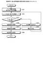
次に、図5を参照して、本実施例に係る携帯電話の信号送信の処理の流れについて説明する。図5は、実施例1に係る携帯電話の信号送信の処理のフローチャートである。 Next, with reference to FIG. 5, the flow of signal transmission processing of the mobile phone according to the present embodiment will be described. FIG. 5 is a flowchart of signal transmission processing of the mobile phone according to the first embodiment.
制御部7は、開閉検知部8が検知した携帯電話の開閉状態の情報を取得する(ステップS101)。 The
次に、制御部7は、送信信号として使用する信号のバンドの情報をBB部5から取得する(ステップS102)。 Next, the
そして、制御部7は、開閉状態の情報及びバンド情報に対応するスイッチ11〜スイッチ13のON/OFFの情報及びFETスイッチ14〜FETスイッチ16の印加電圧の情報である設定情報を取得する(ステップS103)。 And the
制御部7は、取得した設定情報に合わせてスイッチ11〜スイッチ13のON/OFFを制御する。さらに、制御部7は、取得した設定情報に合わせてFETスイッチ14〜FETスイッチ16へ電圧を印加する(ステップS104)。 The
BB部5は、操作者から入力された信号を変調する(ステップS105)。 The
PA14〜PA16のうち送信信号のバンドに応じた増幅器が、変調された送信信号の入力をBB部5から受ける。そして、送信信号の入力を受けた増幅器は、送信信号を増幅する(ステップS106)。 An amplifier corresponding to the band of the transmission signal among PA14 to PA16 receives the input of the modulated transmission signal from the
そして、増幅された送信信号は、アンテナ9から送信される(ステップS107)。 The amplified transmission signal is transmitted from the antenna 9 (step S107).
ここで、図6を参照して、本実施例に係る携帯電話による負荷インピーダンスの変化について説明する。図6は、実施例1に係る携帯電話による負荷インピーダンスの変化を説明するためのスミスチャートである。ここでは、携帯電話は、開いた状態でのインピーダンスが整合するように設計されている場合で説明する。 Here, with reference to FIG. 6, the change of the load impedance by the mobile phone according to the present embodiment will be described. FIG. 6 is a Smith chart for explaining a change in load impedance caused by the mobile phone according to the first embodiment. Here, the case where the cellular phone is designed so that the impedance in the open state is matched will be described.
実線300は、ISOを単に除いただけで、インピーダンスの整合を行わない場合の携帯電話を開いた状態での伝送経路のインピーダンスを表している。詳しくは、実線300は、携帯電話を閉じた状態でのPA41〜43のうち各バンドに対応する増幅器とアンテナとを結ぶ伝送経路の負荷インピーダンスをバンド毎に求めそれらを結んだものである。 A
ここでは、携帯電話を開いた状態でのインピーダンスが整合するように設計されているため、実線300はスミスチャートの中央付近にある。そこで、開いた状態でのインピーダンスの整合を行わなくてもよい。そのため、本実施例に係る携帯電話でもFETスイッチをコンデンサとして用いたインピーダンスの整合は行わない。すなわち、本実施例に係る携帯電話の開いた状態での伝送経路のインピーダンスも実線300で表される。 Here, since the impedance when the cellular phone is opened is designed to match, the
これに対して、点線302は、ISOを単に除いただけで、インピーダンスの整合を行わない場合の携帯電話を閉じた状態での伝送経路のインピーダンスを表している。詳しくは、点線302は、携帯電話を閉じた状態でのPA41〜43のうち各バンドに対応する増幅器とアンテナとを結ぶ伝送経路の負荷インピーダンスをバンド毎に求めそれらを結んだものである。 On the other hand, the dotted
点線302は、スミスチャートの紙面に向かって上側に大きく延びてしまっており、負荷インピーダンスは周波数によって大きく変動している。これでは、使用する周波数によっては増幅器の増幅による歪が大きくなってしまい信号が劣化してしまう。そこで、この場合には、インピーダンスの整合を行うことが好ましい。この場合、伝送経路とグランドとの間にコンデンサとしてみなすことができるFETスイッチを挿入することで、スミスチャートの紙面に向かって左上から右下方向にインピーダンスを変化させることができる。すなわち、本実施例に係る携帯電話を用いることで、点線302で表されるインピーダンスをスミスチャートの紙面に向かって左上から右下方向に向けて移動させることができる。 The dotted
一点鎖線301は、本実施例に係る携帯電話を閉じた状態での伝送経路のインピーダンスを表している。詳しくは、一点鎖線301は、本実施例に係る携帯電話を閉じた状態でのPA41〜43のうち各バンドに対応する増幅器とアンテナとを結ぶ伝送経路の負荷インピーダンスをバンド毎に求めそれらを結んだものである。 An alternate long and
一点鎖線301は、点線302よりもスミスチャートの中心に近づいている。すなわち、本実施例に係る携帯電話の方が、ISOを単に除いただけで、インピーダンスの整合を行わない場合の携帯電話に比べて、負荷インピーダンスが安定している。 The alternate long and
このように、本実施例の携帯電話は、FETスイッチ14〜16を伝送経路とグランドとを結ぶコンデンサとして用いることで、アンテナのインピーダンスが変化した場合の負荷インピーダンスを改善することができる。 As described above, the cellular phone according to the present embodiment can improve the load impedance when the impedance of the antenna changes by using the FET switches 14 to 16 as a capacitor connecting the transmission path and the ground.
以上に説明したように、本実施例に係る無線端末装置は、アンテナスイッチをコンデンサとして用いることにより、アンテナのインピーダンスとPAのインピーダンスとを整合させることができる。これにより、アイソレータをPAとアンテナとの間に設けなくても、アンテナのインピーダンスが変化した影響がPAに及ぶことを抑えることができる。したがって、電力効率を下げずに部品を削減することができる。 As described above, the radio terminal apparatus according to the present embodiment can match the impedance of the antenna and the impedance of the PA by using the antenna switch as a capacitor. Thereby, even if an isolator is not provided between the PA and the antenna, it is possible to suppress the influence of the change in the impedance of the antenna from affecting the PA. Therefore, parts can be reduced without reducing the power efficiency.
図7は、実施例2に係る携帯電話のブロック図である。本実施例に係る携帯電話は、実施例1の携帯電話のスイッチ11〜スイッチ13をFETスイッチに代えたものである。図7において、図1と同じ符号を有する各部は、特に説明の無い限り同じ機能を有するものとする。 FIG. 7 is a block diagram of a mobile phone according to the second embodiment. The mobile phone according to the present embodiment is obtained by replacing the
図7に示すように、本実施例に係る携帯電話のANTスイッチ1は、FETスイッチ14〜FETスイッチ19を有する。 As shown in FIG. 7, the
FETスイッチ17は、アンテナ9とLNA31及びPA41とをDUP21を介して接続する信号の伝送経路上に配置される。本実施例では、FETスイッチ17は、アンテナ9とDUP21との間に設けられている。 The
FETスイッチ17は、FETスイッチ14と同様の構成を有するスイッチである。FETスイッチ17は、送信信号のバンドがBand1の場合、制御部7からの制御を受けて、−0.8V以下の電圧が印加されONとなる。また、FETスイッチ17は、送信信号のバンドがBand2又はBand3の場合、制御部7からの制御を受けて、中間電圧が印加され所定の静電容量を有するコンデンサとなる。 The
FETスイッチ18は、FETスイッチ14と同様の構成を有するスイッチである。FETスイッチ18は、送信信号のバンドがBand2の場合、制御部7からの制御を受けて、−0.8V以下の電圧が印加されONとなる。また、FETスイッチ18は、送信信号のバンドがBand1又はBand3の場合、制御部7からの制御を受けて、中間電圧が印加され所定の静電容量を有するコンデンサとなる。 The
FETスイッチ19は、FETスイッチ14と同様の構成を有するスイッチである。FETスイッチ19は、送信信号のバンドがBand3の場合、制御部7からの制御を受けて、−0.8V以下の電圧が印加されONとなる。また、FETスイッチ19は、送信信号のバンドがBand1又はBand2の場合、制御部7からの制御を受けて、中間電圧が印加され所定の静電容量を有するコンデンサとなる。このFETスイッチ17〜19が、「第1スイッチ」の一例にあたる。 The
図8は、実施例2に係る携帯電話のANTスイッチ部の回路例を示す図である。端子T1は、FETスイッチ14のゲート端子に接続されている。端子T2は、FETスイッチ15のゲート端子に接続されている。端子T3は、FETスイッチ16のゲート端子に接続されている。端子T4は、FETスイッチ17のゲート端子に接続されている。端子T5は、FETスイッチ18のゲート端子に接続されている。端子T6は、FETスイッチ19のゲート端子に接続されている。端子T1〜T6にはそれぞれ異なる電圧をかけることができる。これにより、FETスイッチ14〜FETスイッチ19のそれぞれにゲート電圧を異ならせて印加することができる。 FIG. 8 is a diagram illustrating a circuit example of the ANT switch unit of the mobile phone according to the second embodiment. The terminal T1 is connected to the gate terminal of the
図9は、実施例2に係る携帯電話の設定情報テーブルの一例の図である。図9に示すように、本実施例では、設定情報テーブル400には、バンド、開閉状態及び印加電圧の項目が設けられている。設定情報テーブル400の印加電圧の項には、バンド情報及び開閉状態の組に対応するFETスイッチ14〜FETスイッチ19のそれぞれに印加する電圧が記載されている。 FIG. 9 is a diagram of an example of a setting information table for a mobile phone according to the second embodiment. As shown in FIG. 9, in the present embodiment, the setting information table 400 includes items of band, open / close state, and applied voltage. The applied voltage section of the setting information table 400 describes the voltage applied to each of the
例えば、送信信号のバンドがBand1かつ携帯電話が閉じた状態の場合について説明する。この場合、対応するFETスイッチ14〜FETスイッチ19のそれぞれに印加する電圧は、V’1(2)〜V’6(2)となる。ここで、送信信号のバンドがBand1の場合、PA41で送信信号を増幅し、その増幅した送信信号をアンテナ9から送信するので、FETスイッチ17はONとなる。そこで、V’4(2)は、−0.8Vよりも高い電圧である。この場合、FETスイッチ17がONであり、PA41で増幅された送信信号はDUP21及びスイッチ11を経由してアンテナ9から送信される。そして、V’1(2)、V’2(2)、V’3(2)、V’5(2)及びV’6(2)は、それらの電圧を印加した場合のFETスイッチ14〜16、18及び19の静電容量によりアンテナ9のインピーダンスとPA41の出力インピーダンスとの整合が取れるように決定されている。言い換えれば、アンテナ9とPA41とを結ぶ伝送路の負荷インピーダンスをスミスチャートで表した場合に、表された負荷インピーダンスがスミスチャートの中心部に近づくようにFETスイッチ14〜16、18及び19の静電容量が決定される。そして、その決定された静電容量をFETスイッチ14〜16、18及び19が有する電圧がV’1(2)、V’2(2)、V’3(2)、V’5(2)及びV’6(2)である。 For example, a case where the band of the transmission signal is Band1 and the mobile phone is closed will be described. In this case, the voltages applied to the corresponding FET switches 14 to 19 are V′1 (2) to V′6 (2). Here, when the band of the transmission signal is Band1, the transmission signal is amplified by the
ここで、図9の設定情報テーブル400には、3通りの設定情報が記載されているが、実際には、使用するバンド数とそれに対応する開閉状態の数の設定情報が、設定情報テーブル400に記載されている。また、ここでは送信信号のバンドがBand1かつ携帯電話が閉じた状態の場合の印加電圧について説明したが、バンドや開閉状態が他の場合においても、同様に印加電圧が決定される。 Here, although three types of setting information are described in the setting information table 400 of FIG. 9, the setting information of the number of bands to be used and the number of open / close states corresponding thereto is actually set in the setting information table 400. It is described in. Further, here, the applied voltage when the band of the transmission signal is
次に、図10を参照して、本実施例に係る携帯電話の信号送信の処理の流れについて説明する。図10は、実施例2に係る携帯電話の信号送信の処理のフローチャートである。 Next, with reference to FIG. 10, the flow of signal transmission processing of the mobile phone according to the present embodiment will be described. FIG. 10 is a flowchart of signal transmission processing of the mobile phone according to the second embodiment.
制御部7は、開閉検知部8が検知した携帯電話の開閉状態の情報を取得する(ステップS201)。 The
次に、制御部7は、送信信号として使用する信号のバンドの情報をBB部5から取得する(ステップS202)。 Next, the
そして、制御部7は、開閉状態の情報及びバンド情報に対応するFETスイッチ14〜FETスイッチ19の印加電圧の情報である設定情報を取得する(ステップS203)。 And the
制御部7は、取得した設定情報に合わせてFETスイッチ14〜FETスイッチ19へ電圧を印加する(ステップS204)。 The
BB部5は、操作者から入力された信号を変調する(ステップS205)。 The
PA41〜PA43のうち送信信号のバンドに応じた増幅器が、変調された送信信号の入力をBB部5から受ける。そして、送信信号の入力を受けた増幅器は、送信信号を増幅する(ステップS206)。 An amplifier corresponding to the band of the transmission signal among PA41 to PA43 receives the input of the modulated transmission signal from the
そして、増幅された送信信号は、アンテナ9から送信される(ステップS207)。 The amplified transmission signal is transmitted from the antenna 9 (step S207).
以上に説明したように、本実施例に係る携帯電話は、伝送経路とグランドとの間に配置されたコンデンサとみなせるFETスイッチに加えて、伝送経路上にコンデンサとみなせるFETスイッチを配置している。これにより、伝送経路上に配置されたFETスイッチを、アンテナのインピーダンスとPAの出力インピーダンスとの整合に用いることができる。ここで、伝送経路とグランドとの間のコンデンサの静電容量の調整では、整合できる範囲は容量性の領域に限られ、調整できる範囲がスミスチャートの上半分に限定されてしまうおそれがある。これでは、アンテナのインピーダンスが誘導性となった場合に対応ができない。これに対して、伝送経路上のコンデンサの静電容量を調整することで、誘導性の領域に対しても整合を行うことができる。すなわち、本実施例に係る無線端末装置を用いることで、許容性及び許容性のいずれの領域に対しても整合を行うことができる。したがって、実施例1の場合に比べて、本実施例に係る無線端末装置ではアンテナのインピーダンスの変化に対して整合を行える範囲を広げることができ、より適切にインピーダンスの整合を行うことができる。 As described above, the cellular phone according to the present embodiment includes an FET switch that can be regarded as a capacitor on the transmission path in addition to the FET switch that can be regarded as a capacitor disposed between the transmission path and the ground. . As a result, the FET switch arranged on the transmission path can be used for matching the impedance of the antenna and the output impedance of the PA. Here, in the adjustment of the capacitance of the capacitor between the transmission path and the ground, the matching range is limited to the capacitive region, and the adjustable range may be limited to the upper half of the Smith chart. This cannot cope with the case where the impedance of the antenna becomes inductive. On the other hand, by adjusting the capacitance of the capacitor on the transmission path, matching can be performed for the inductive region. That is, by using the wireless terminal device according to the present embodiment, it is possible to perform matching for both areas of tolerance and tolerance. Therefore, compared with the case of the first embodiment, in the wireless terminal device according to the present embodiment, the range in which matching can be performed with respect to changes in the impedance of the antenna can be expanded, and impedance matching can be performed more appropriately.
図11は、実施例3に係る携帯電話のブロック図である。本実施例に係る携帯電話は、アンテナのインピーダンスの変化を取得して、その変化に応じて印加電圧を変化させることが実施例1及び実施例2と異なるものである。そこで、以下では、アンテナのインピーダンスの検出及び検出したインピーダンスによる印加電圧の調整について主に説明する。図11において、図1と同じ符号を有する各部は、特に説明の無い限り同じ機能を有するものとする。また、以下の説明では、実施例1を基にした場合の説明を行うが、実施例2に本実施例の機能を加えることもでき、その場合にも同様の効果を奏する。 FIG. 11 is a block diagram of a mobile phone according to the third embodiment. The cellular phone according to the present embodiment is different from the first embodiment and the second embodiment in that the change in the impedance of the antenna is acquired and the applied voltage is changed in accordance with the change. Therefore, hereinafter, the detection of the impedance of the antenna and the adjustment of the applied voltage based on the detected impedance will be mainly described. In FIG. 11, parts having the same reference numerals as those in FIG. 1 have the same functions unless otherwise specified. Further, in the following description, the case based on the first embodiment will be described. However, the function of the present embodiment can be added to the second embodiment, and the same effect can be obtained in that case.
本実施例に係る携帯電話は、図11に示すように、インピーダンス検出部10が、アンテナ9とANTスイッチ1の間に配置されている。また、この場合、図1における開閉検知部8を設けなくてもよく、本実施例では、開閉検知部8を設けない場合で説明する。図12は、インピーダンス検出部の詳細を表すブロック図である。 In the mobile phone according to this embodiment, as shown in FIG. 11, the
インピーダンス検出部10は、図12に示すように、PREV(Power Reverse:反射波電力)取得部101、PFRD(Power Forward:進行波電力)取得部102及びインピーダンス算出部103を有している。インピーダンス検出部10が、「インピーダンス取得部」の一例にあたる。 As shown in FIG. 12, the
アンテナ9のインピーダンスの影響で反射波が発生している。そして、PREV取得部101は、アンテナ9のインピーダンスによる反射波の電力を取得する。そして、PREV取得部101は、取得した反射波電力をインピーダンス算出部103へ出力する。 A reflected wave is generated due to the influence of the impedance of the antenna 9. Then, the
PFRD取得部102は、ANTスイッチ1からアンテナ9に向かう進行波の電力を取得する。そして、PFRD取得部102は、取得した進行波電力をインピーダンス算出部103へ出力する。 The
インピーダンス算出部103は、反射波電力の入力をPREV取得部101から受ける。また、インピーダンス算出部103は、進行波電力の入力をPFRD取得部102から受ける。そして、インピーダンス算出部103は、進行波電力と反射波電力との比を求めることで、アンテナ9のインピーダンスを算出する。そして、インピーダンス算出部103は、算出したアンテナ9のインピーダンスを制御部7へ出力する。 The
制御部7は、アンテナ9のインピーダンスの入力をインピーダンス算出部103から受ける。そして、制御部7は、受信したアンテナ9のインピーダンスに応じて、FETスイッチ14〜16のそれぞれに対して印加する電圧を変化させそれぞれの静電容量を調整する。そして、制御部7は、インピーダンス算出部103から入力されるアンテナ9のインピーダンスが所定値になるまでFETスイッチ14〜16の静電容量の調整を行う。ここで、本実施例では、制御部7は、アンテナ9のインピーダンスの所定値を10dBとしている。 The
ここで、図13を参照して、制御部7によるアンテナ9のインピーダンスの調整の一例を説明する。図13は、検出されたアンテナのインピーダンスに対する印加電圧の制御を説明するための図である。図13の横軸はゲートソース間電圧を表しており、縦軸はドレイン電流を表している。そして、実線がFETスイッチ14の伝達特性500を表している。この伝達特性は、FETスイッチ15及び16でも同じである。ここで、アンテナ9のインピーダンスは、ΔVGS/ΔIDSとなる。例えば、点線で表されるΔVGSに対応するΔIDSは一点鎖線で表される。この場合、点線と一点鎖線とが形成する直角三角形の斜辺の傾きがアンテナ9のインピーダンスとなる。すなわち、伝達特性500の傾きがゆるければ、アンテナ9のインピーダンスが高いことを示している。また、伝達特性500の傾きが急であれば、アンテナ9のインピーダンスが低いことを示している。すなわち、伝達特性500は、電圧を高くするとインピーダンスが下がることを示している。Here, an example of adjustment of the impedance of the antenna 9 by the
制御部7は、図13に示すFETスイッチ14〜16の伝達特性を記憶しておく。そして、制御部7は、記憶している伝達特性から受信したアンテナ9のインピーダンスを10dBにするように、各FETスイッチ14〜16の電圧を高くするか低くするかを決める。そして、制御部7は、FETスイッチ14〜16のそれぞれに印加している電圧を、決定した電圧に変化させる。このようにして、制御部7は、アンテナ9のインピーダンスが所定値になるように調整を行う。 The
次に、図14を参照して、本実施例に係る携帯電話の信号送信の処理の流れについて説明する。図14は、実施例3に係る携帯電話の信号送信の処理のフローチャートである。 Next, with reference to FIG. 14, the flow of signal transmission processing of the mobile phone according to the present embodiment will be described. FIG. 14 is a flowchart of signal transmission processing of the mobile phone according to the third embodiment.
制御部7は、送信信号として使用する信号のバンドの情報をBB部5から取得する。そして、制御部7は、バンド情報に合わせてスイッチ11〜スイッチ13のON/OFFを制御する(ステップS301)。 The
インピーダンス検出部10は、アンテナ9のインピーダンスを検出する(ステップS302)。 The
制御部7は、アンテナ9のインピーダンスの入力をインピーダンス検出部10から受ける。そして、制御部7は、受信したアンテナ9のインピーダンスが所定値か否かを判定する(ステップS303)。 The
アンテナ9のインピーダンスが所定値でない場合(ステップS303否定)、制御部7は、受信したアンテナ9のインピーダンスが所定値に近づくようにFETスイッチ14〜FETスイッチ16の印加電圧を求める(ステップS304)。 When the impedance of the antenna 9 is not a predetermined value (No at Step S303), the
制御部7は、求めた印加電圧をFETスイッチ14〜FETスイッチ16のそれぞれへ印加する(ステップS305)。その後、ステップS302へ戻る。 The
これに対して、アンテナ9のインピーダンスが所定値の場合(ステップS303肯定)、BB部5は、操作者から入力された信号を変調する(ステップS306)。 On the other hand, when the impedance of the antenna 9 is a predetermined value (Yes at Step S303), the
そして、PA41〜PA43のうち送信信号のバンドに応じた増幅器が、変調された送信信号の入力をBB部5から受ける。そして、送信信号の入力を受けた増幅器は、送信信号を増幅する(ステップS307)。 Then, the amplifier corresponding to the band of the transmission signal among PA41 to PA43 receives the input of the modulated transmission signal from the
そして、増幅された送信信号は、アンテナ9から送信される(ステップS308)。 The amplified transmission signal is transmitted from the antenna 9 (step S308).
以上に説明したように、本実施例に係る携帯電話は、アンテナのインピーダンスを検出し、検出したインピーダンスを基にFETスイッチの静電容量を調整して、アンテナインピーダンスとPAの出力インピーダンスとを整合させる。これにより、本実施例に係る無線端末装置は、実施例1及び実施例2の場合に比べてより適切にアンテナインピーダンスとPAの出力インピーダンスとを整合させることができる。また、本実施例に係る無線端末装置によれば、アンテナのインピーダンスのどのような変化に対しても、適切にアンテナインピーダンスとPAの出力インピーダンスとを整合させることができる。 As described above, the mobile phone according to this embodiment detects the impedance of the antenna, adjusts the capacitance of the FET switch based on the detected impedance, and matches the antenna impedance and the output impedance of the PA. Let Thereby, the radio | wireless terminal apparatus which concerns on a present Example can match an antenna impedance and the output impedance of PA more appropriately compared with the case of Example 1 and Example 2. FIG. Moreover, according to the wireless terminal device according to the present embodiment, it is possible to appropriately match the antenna impedance and the output impedance of the PA for any change in the impedance of the antenna.
また、以上の各実施例では、3つのバンドを使用する場合で説明したが、バンドの数には特に制限は無い。 In each of the above embodiments, the case where three bands are used has been described. However, the number of bands is not particularly limited.
1 ANTスイッチ
5 BB部
6 記憶部
7 制御部
8 開閉検知部
9 アンテナ
10 インピーダンス検出部
11〜13 スイッチ
14〜19 FETスイッチ
21〜23 DUP
31〜33 LNA
41〜43 PA
101 RREV取得部
102 PFRD取得部
103 インピーダンス算出部DESCRIPTION OF
31-33 LNA
41-43 PA
101
Claims (5)
Translated fromJapanese前記第一の筐体と可変自在に連結される第二の筐体と、
を備える無線端末装置であって、
送信信号を生成するベースバンド処理部と、
前記送信信号を増幅する複数の増幅器と、
前記アンテナと前記増幅器のそれぞれとを結ぶ各伝送経路上に設けられた第1スイッチと、
前記伝送経路とグランドとの間に設けられ、第1の所定電圧を印加するとONになり、第2の所定電圧を印加するとOFFになり、前記第1の所定電圧と前記第2の所定電圧との中間電圧を印加した場合、印加した中間電圧に応じた静電容量を発生させる第2スイッチと、
前記第一の筐体と前記第二の筐体との位置関係に対応した前記アンテナのインピーダンスを取得するインピーダンス取得部と、
前記送信信号の周波数帯を基に、前記第1スイッチのいずれか一つをONにし、且つ前記インピーダンス取得部により取得された前記アンテナのインピーダンスを基に、前記第1スイッチがONになっている伝送経路に配置された前記増幅器のインピーダンスと前記アンテナのインピーダンスとが整合するように前記第2スイッチの少なくとも一つに対して前記中間電圧を印加する制御部と、
を備えたことを特徴とする無線端末装置。A first housing with an antenna;
A second housing variably coupled to the first housing;
A wireless terminal device comprising:
A baseband processing unit for generating a transmission signal;
A plurality of amplifiers for amplifying the transmission signal;
A first switch provided on each transmission path connecting the antenna and the amplifier;
Provided between the transmission path and the ground, it is turned on when a first predetermined voltage is applied, and is turned off when a second predetermined voltage is applied, and the first predetermined voltage and the second predetermined voltage are A second switch thatgenerates a capacitance according to the applied intermediate voltage;
An impedance acquisition unit that acquires the impedance of the antenna corresponding to the positional relationship between the first casing and the second casing;
One of the first switches is turned on based on the frequency band of the transmission signal, and the first switch is turned on based on the impedance of the antenna acquired by the impedance acquisition unit. A controller that applies the intermediate voltage to at least one of the second switches so that an impedance of the amplifier disposed in a transmission path matches an impedance of the antenna;
A wireless terminal device comprising:
前記制御部は、前記インピーダンス取得部により検出されるアンテナのインピーダンスが所定の値になるように前記第2スイッチの静電容量を制御することを特徴とする請求項1に記載の無線端末装置。The impedance acquisition unit detects the impedance of the antenna based on a reflected wave from the antenna and a traveling wave toward the antenna,
The radio terminal apparatus according to claim 1, wherein the control unit controls the capacitance of the second switch so that the impedance of the antenna detected by the impedance acquisition unit becomes a predetermined value.
前記制御部は、送信信号の周波数帯及び前記アンテナのインピーダンスを基に、前記第1スイッチのいずれか一つに対して第2の所定電圧を印加し、且つ前記インピーダンス取得部により取得された前記アンテナのインピーダンスを基に、前記第1スイッチがONになっている伝送経路に配置された前記増幅器のインピーダンスと前記アンテナのインピーダンスとを整合させる静電容量を有するように他の各前記第1スイッチ及び各前記第2スイッチに対して前記中間電圧を印加する
ことを特徴とする請求項1〜請求項4のいずれか一つに記載の無線端末装置。The first switch is turned on when the first predetermined voltage is applied, is turned off when the second predetermined voltage is applied, and an intermediate voltage between the first predetermined voltage and the second predetermined voltage is applied. When thisoccurs, it generates a capacitance according to the applied intermediate voltage,
The control unit applies a second predetermined voltage to any one of the first switches based on a frequency band of a transmission signal and an impedance of the antenna, and is acquired by the impedance acquisition unit. Based on the impedance of the antenna, each of the other first switches has a capacitance that matches the impedance of the amplifier and the impedance of the antenna arranged in the transmission path in which the first switch is ON. And the said intermediate voltage is applied with respect to each said 2nd switch. The radio | wireless terminal apparatus as described in any one of Claims 1-4 characterized by the above-mentioned.
Priority Applications (5)
| Application Number | Priority Date | Filing Date | Title |
|---|---|---|---|
| JP2011061763AJP5672098B2 (en) | 2011-03-18 | 2011-03-18 | Wireless terminal device |
| EP12151773.4AEP2501050B1 (en) | 2011-03-18 | 2012-01-19 | Wireless terminal device |
| US13/354,494US8478334B2 (en) | 2011-03-18 | 2012-01-20 | Wireless terminal device |
| KR1020120010097AKR101384043B1 (en) | 2011-03-18 | 2012-01-31 | Wireless terminal device |
| CN201210021386.5ACN102684728B (en) | 2011-03-18 | 2012-01-31 | Wireless terminal device |
Applications Claiming Priority (1)
| Application Number | Priority Date | Filing Date | Title |
|---|---|---|---|
| JP2011061763AJP5672098B2 (en) | 2011-03-18 | 2011-03-18 | Wireless terminal device |
Publications (2)
| Publication Number | Publication Date |
|---|---|
| JP2012199710A JP2012199710A (en) | 2012-10-18 |
| JP5672098B2true JP5672098B2 (en) | 2015-02-18 |
Family
ID=45558551
Family Applications (1)
| Application Number | Title | Priority Date | Filing Date |
|---|---|---|---|
| JP2011061763AActiveJP5672098B2 (en) | 2011-03-18 | 2011-03-18 | Wireless terminal device |
Country Status (5)
| Country | Link |
|---|---|
| US (1) | US8478334B2 (en) |
| EP (1) | EP2501050B1 (en) |
| JP (1) | JP5672098B2 (en) |
| KR (1) | KR101384043B1 (en) |
| CN (1) | CN102684728B (en) |
Families Citing this family (18)
| Publication number | Priority date | Publication date | Assignee | Title |
|---|---|---|---|---|
| US9054756B2 (en) | 2011-09-19 | 2015-06-09 | Qualcomm Incorporated | Adaptive tuning of an impedance matching circuit in a wireless device |
| TWI552431B (en)* | 2012-09-04 | 2016-10-01 | 深圳市華星光電技術有限公司 | Communication apparatus equipped with switchable antenna |
| US9240811B2 (en) | 2012-10-23 | 2016-01-19 | Intel Deutschland Gmbh | Switched duplexer front end |
| KR101712976B1 (en)* | 2013-06-26 | 2017-03-22 | 인텔 아이피 코포레이션 | Bulk acoustic wave resonator tuner circuits |
| US10009193B2 (en) | 2015-02-23 | 2018-06-26 | Photonic Systems, Inc. | Methods and apparatus for source and load power transfer control |
| CN110661543B (en)* | 2015-07-17 | 2021-07-06 | 苹果公司 | Mobile phone device, radio frequency transceiver circuit and impedance adjusting device |
| JP6471810B2 (en)* | 2015-11-04 | 2019-02-20 | 株式会社村田製作所 | Demultiplexer and design method thereof |
| US10141958B2 (en)* | 2016-02-19 | 2018-11-27 | Psemi Corporation | Adaptive tuning network for combinable filters |
| US10700658B2 (en) | 2016-02-19 | 2020-06-30 | Psemi Corporation | Adaptive tuning networks with direct mapped multiple channel filter tuning |
| US11329630B2 (en) | 2016-05-12 | 2022-05-10 | Murata Manufacturing Co., Ltd. | Switch module |
| US10944382B2 (en) | 2016-05-12 | 2021-03-09 | Murata Manufacturing Co., Ltd. | Switch module |
| JP6790447B2 (en)* | 2016-05-12 | 2020-11-25 | 株式会社村田製作所 | Switch module |
| JP6779842B2 (en)* | 2016-12-14 | 2020-11-04 | 株式会社東芝 | Semiconductor device |
| CN108900206A (en)* | 2018-07-04 | 2018-11-27 | 青岛海信移动通信技术股份有限公司 | A kind of impedance-matching device, impedance matching methods and communication terminal |
| DE102018215763A1 (en)* | 2018-09-17 | 2020-03-19 | Bayerische Motoren Werke Aktiengesellschaft | Radio receiving device of a motor vehicle |
| US11018703B2 (en)* | 2018-09-21 | 2021-05-25 | Qualcomm Incorporated | Systems and methods for antenna tuning |
| DE102018220994A1 (en)* | 2018-12-05 | 2020-06-10 | Rheinisch-Westfälische Technische Hochschule (Rwth) Aachen | Electrical switch with improved insulation and insertion loss |
| CN112152648B (en)* | 2020-09-08 | 2022-08-12 | Oppo广东移动通信有限公司 | Radio frequency circuit, power adjustment method and communication terminal |
Family Cites Families (20)
| Publication number | Priority date | Publication date | Assignee | Title |
|---|---|---|---|---|
| JPH0832431A (en)* | 1994-07-11 | 1996-02-02 | Shimada Phys & Chem Ind Co Ltd | Signal switch |
| JPH08330996A (en)* | 1995-05-30 | 1996-12-13 | Sony Corp | Antenna multicoupler |
| JPH09270659A (en) | 1996-01-31 | 1997-10-14 | Matsushita Electric Ind Co Ltd | Switch attenuator |
| US5777530A (en) | 1996-01-31 | 1998-07-07 | Matsushita Electric Industrial Co., Ltd. | Switch attenuator |
| JP2001217663A (en)* | 2000-02-02 | 2001-08-10 | Nec Saitama Ltd | Transmission circuit |
| JP2003087149A (en) | 2001-09-14 | 2003-03-20 | Matsushita Electric Ind Co Ltd | High frequency composite switch module |
| JP2003158468A (en)* | 2001-11-20 | 2003-05-30 | Toshiba Corp | Portable wireless devices |
| US7512386B2 (en)* | 2003-08-29 | 2009-03-31 | Nokia Corporation | Method and apparatus providing integrated load matching using adaptive power amplifier compensation |
| JP4340511B2 (en)* | 2003-10-21 | 2009-10-07 | 株式会社日立国際電気 | Automatic impedance matching method |
| KR20060073197A (en)* | 2004-12-24 | 2006-06-28 | 주식회사 팬택앤큐리텔 | Antenna automatic matching device of mobile communication terminal |
| JP2006229333A (en)* | 2005-02-15 | 2006-08-31 | Sony Corp | Wireless communication device |
| JP2006324984A (en)* | 2005-05-19 | 2006-11-30 | Matsushita Electric Ind Co Ltd | Wireless communication device |
| JP2007143031A (en)* | 2005-11-22 | 2007-06-07 | Staf Corp | Antenna matching circuit |
| CN101064917A (en)* | 2006-04-28 | 2007-10-31 | 佛山市顺德区顺达电脑厂有限公司 | Wireless communication system having plurality of matching apparatus |
| JP4662211B2 (en)* | 2006-09-12 | 2011-03-30 | 株式会社デンソー | In-vehicle wireless transmitter |
| CN101536327B (en)* | 2006-11-09 | 2013-03-13 | 瑞萨电子株式会社 | Semiconductor integrated circuit, RF module incorporating it, and wireless communication terminal device incorporating it |
| JP2008244723A (en)* | 2007-03-27 | 2008-10-09 | Kyocera Corp | Radio apparatus and amplifier circuit |
| JP5029946B2 (en)* | 2007-04-24 | 2012-09-19 | 日立金属株式会社 | Switch module |
| CN201069869Y (en)* | 2007-04-25 | 2008-06-04 | 华为技术有限公司 | Clamshell communication terminal and the antenna system for this terminal |
| JP5237842B2 (en)* | 2009-01-29 | 2013-07-17 | ルネサスエレクトロニクス株式会社 | Semiconductor device |
- 2011
- 2011-03-18JPJP2011061763Apatent/JP5672098B2/enactiveActive
- 2012
- 2012-01-19EPEP12151773.4Apatent/EP2501050B1/ennot_activeNot-in-force
- 2012-01-20USUS13/354,494patent/US8478334B2/enactiveActive
- 2012-01-31KRKR1020120010097Apatent/KR101384043B1/ennot_activeExpired - Fee Related
- 2012-01-31CNCN201210021386.5Apatent/CN102684728B/ennot_activeExpired - Fee Related
Also Published As
| Publication number | Publication date |
|---|---|
| EP2501050A3 (en) | 2015-11-25 |
| CN102684728B (en) | 2015-07-08 |
| EP2501050A2 (en) | 2012-09-19 |
| EP2501050B1 (en) | 2016-09-14 |
| US20120238224A1 (en) | 2012-09-20 |
| US8478334B2 (en) | 2013-07-02 |
| JP2012199710A (en) | 2012-10-18 |
| CN102684728A (en) | 2012-09-19 |
| KR20120106551A (en) | 2012-09-26 |
| KR101384043B1 (en) | 2014-04-09 |
Similar Documents
| Publication | Publication Date | Title |
|---|---|---|
| JP5672098B2 (en) | Wireless terminal device | |
| KR102287445B1 (en) | System and method for bypassing a low noise amplifier | |
| KR102836149B1 (en) | Load line switching for push-pull power amplifiers | |
| US10476460B2 (en) | Low-noise amplifier having programmable-phase gain stage | |
| JP5763485B2 (en) | Antenna switch and communication device | |
| US10147990B2 (en) | Low-noise amplifier with low-loss bypass mode | |
| US20190058444A1 (en) | Power amplifier module | |
| US7898325B2 (en) | Amplifier with bypass switch | |
| KR20120024486A (en) | Apparatus and method for a tunable multi-band power amplifier module | |
| CN103534940A (en) | Positive feedback common gate low noise amplifier | |
| KR20200005465A (en) | Amplifier linearity boost circuits and methods for post distortion feedback cancelation | |
| US20190131941A1 (en) | Power amplifier circuit | |
| US7868697B2 (en) | Converting circuit for converting differential signal to single-ended signal | |
| JP5594372B2 (en) | Matching device, transmission amplifier, and wireless communication device | |
| US20250007472A1 (en) | Distortion network with channelized resistors | |
| US20150188501A1 (en) | Power amplifying apparatus | |
| CN111313839B (en) | Amplifying circuit | |
| US10756727B2 (en) | Switching circuit and high-frequency module | |
| JP2021083010A (en) | Power amplification circuit | |
| US12381519B2 (en) | Broadband low noise amplifier using multiple cascode stages | |
| US20210391834A1 (en) | Power amplifier module | |
| JP5807541B2 (en) | RF power amplifier module | |
| US20020163382A1 (en) | High dynamic range amplification circuit | |
| JP2007221308A (en) | Power amplifier and high-frequency communication device | |
| HK40058385A (en) | Load-line switching for push-pull power amplifiers |
Legal Events
| Date | Code | Title | Description |
|---|---|---|---|
| A621 | Written request for application examination | Free format text:JAPANESE INTERMEDIATE CODE: A621 Effective date:20140108 | |
| A977 | Report on retrieval | Free format text:JAPANESE INTERMEDIATE CODE: A971007 Effective date:20140829 | |
| A131 | Notification of reasons for refusal | Free format text:JAPANESE INTERMEDIATE CODE: A131 Effective date:20140902 | |
| A521 | Request for written amendment filed | Free format text:JAPANESE INTERMEDIATE CODE: A523 Effective date:20141104 | |
| TRDD | Decision of grant or rejection written | ||
| A01 | Written decision to grant a patent or to grant a registration (utility model) | Free format text:JAPANESE INTERMEDIATE CODE: A01 Effective date:20141125 | |
| A61 | First payment of annual fees (during grant procedure) | Free format text:JAPANESE INTERMEDIATE CODE: A61 Effective date:20141208 | |
| R150 | Certificate of patent or registration of utility model | Ref document number:5672098 Country of ref document:JP Free format text:JAPANESE INTERMEDIATE CODE: R150 | |
| S111 | Request for change of ownership or part of ownership | Free format text:JAPANESE INTERMEDIATE CODE: R313113 | |
| R350 | Written notification of registration of transfer | Free format text:JAPANESE INTERMEDIATE CODE: R350 | |
| R250 | Receipt of annual fees | Free format text:JAPANESE INTERMEDIATE CODE: R250 | |
| S531 | Written request for registration of change of domicile | Free format text:JAPANESE INTERMEDIATE CODE: R313531 | |
| S533 | Written request for registration of change of name | Free format text:JAPANESE INTERMEDIATE CODE: R313533 | |
| R350 | Written notification of registration of transfer | Free format text:JAPANESE INTERMEDIATE CODE: R350 | |
| R250 | Receipt of annual fees | Free format text:JAPANESE INTERMEDIATE CODE: R250 | |
| R250 | Receipt of annual fees | Free format text:JAPANESE INTERMEDIATE CODE: R250 | |
| R250 | Receipt of annual fees | Free format text:JAPANESE INTERMEDIATE CODE: R250 | |
| S111 | Request for change of ownership or part of ownership | Free format text:JAPANESE INTERMEDIATE CODE: R313113 | |
| S533 | Written request for registration of change of name | Free format text:JAPANESE INTERMEDIATE CODE: R313533 | |
| R350 | Written notification of registration of transfer | Free format text:JAPANESE INTERMEDIATE CODE: R350 | |
| R250 | Receipt of annual fees | Free format text:JAPANESE INTERMEDIATE CODE: R250 |