JP5671784B2 - Letterpress for printing, method for producing electronic device using the letterpress for printing, and organic electroluminescence element - Google Patents
Letterpress for printing, method for producing electronic device using the letterpress for printing, and organic electroluminescence elementDownload PDFInfo
- Publication number
- JP5671784B2 JP5671784B2JP2009089869AJP2009089869AJP5671784B2JP 5671784 B2JP5671784 B2JP 5671784B2JP 2009089869 AJP2009089869 AJP 2009089869AJP 2009089869 AJP2009089869 AJP 2009089869AJP 5671784 B2JP5671784 B2JP 5671784B2
- Authority
- JP
- Japan
- Prior art keywords
- printing
- convex
- organic
- ink
- layer
- Prior art date
- Legal status (The legal status is an assumption and is not a legal conclusion. Google has not performed a legal analysis and makes no representation as to the accuracy of the status listed.)
- Expired - Fee Related
Links
Images


Landscapes
- Printing Methods (AREA)
- Printing Plates And Materials Therefor (AREA)
- Electroluminescent Light Sources (AREA)
Description
Translated fromJapanese本発明は、電子デバイスを凸版印刷法によって作製するために用いられる印刷用凸版、該印刷用凸版を用いた電子デバイスの製造方法、有機エレクトロルミネッセンス素子に関するものである。 The present invention relates to a printing relief plate used for producing an electronic device by a relief printing method, an electronic device manufacturing method using the printing relief plate, and an organic electroluminescence element.
有機エレクトロルミネッセンス素子は、対向する陽極と陰極との間に有機発光材料からなる有機発光層が形成された構造をもつ発光素子であり、電圧の印加によって陽極、陰極からそれぞれ正孔、電子が注入され、それらが有機発光層で再結合を起こすことにより発光させるものであるが、効率の良い発光を得るためには、有機発光層の膜厚が重要な要素であり、数nmから数十nm程度で膜厚をコントロールする必要がある。さらに、これをディスプレイ化するには高精細にパターニングする必要がある。 An organic electroluminescent element is a light emitting element having a structure in which an organic light emitting layer made of an organic light emitting material is formed between an anode and a cathode facing each other, and holes and electrons are injected from the anode and the cathode, respectively, by applying a voltage. However, in order to obtain light emission by causing recombination in the organic light emitting layer, the film thickness of the organic light emitting layer is an important factor for obtaining efficient light emission, from several nm to several tens of nm. It is necessary to control the film thickness by the degree. Further, in order to make this a display, it is necessary to pattern it with high definition.
有機発光層に用いられる有機発光材料は、低分子系材料と高分子系材料に区分されており、有機発光層の形成方法は有機発光材料の種類によって異なる。 The organic light emitting material used for the organic light emitting layer is classified into a low molecular material and a polymer material, and the method of forming the organic light emitting layer differs depending on the type of the organic light emitting material.
一般に低分子系材料は、基板に抵抗加熱蒸着法(真空蒸着法)等によって薄膜形成する。有機エレクトロルミネッセンス素子をフルカラー化する場合には、各色の画素形状に応じたパターンのマスクを用いて、異なる発光色の発光材料をそれぞれの画素部分に蒸着して形成する方法が採用されている。この方法は、薄膜形状を均一に形成するには優れた方法であるが、蒸着される基板が大型になるとマスクのパターン精度が出難くなるという問題点がある。 In general, a low molecular weight material is formed into a thin film on a substrate by resistance heating vapor deposition (vacuum vapor deposition) or the like. In the case of full-color organic electroluminescence elements, a method is employed in which a luminescent material having a different emission color is deposited on each pixel portion using a mask having a pattern corresponding to the pixel shape of each color. Although this method is an excellent method for uniformly forming a thin film shape, there is a problem in that the mask pattern accuracy is difficult to be obtained when the deposited substrate becomes large.
一方で高分子系材料では、有機発光材料を溶剤に溶解あるいは分散させてインキ化し、これをウェットコーティング法によって薄膜を形成する方法が主に用いられている。ウェットコーティング法としては、スピンコート法、バーコート法、突出コート法、ディップコート法等があるが、高精細なパターニングや、フルカラー化の色の塗り分けにこれらの方法を用いることは困難である。そこで、フルカラー化に有機発光材層をパターニングする手段としては、インキジェット法や印刷法によるパターン印刷が有効であると考えられる。 On the other hand, in the case of polymer materials, a method in which an organic light emitting material is dissolved or dispersed in a solvent to form an ink and a thin film is formed by a wet coating method is mainly used. As the wet coating method, there are a spin coating method, a bar coating method, a protruding coating method, a dip coating method, etc., but it is difficult to use these methods for high-definition patterning and color separation for full color. . Therefore, it is considered that pattern printing by an ink jet method or a printing method is effective as a means for patterning the organic light emitting material layer for full color.
ここで、例えば(特許文献1)に開示されているインキジェット法によるパターン形成方法は、インキジェットノズルから溶剤に溶かした有機発光材料を基板上に噴出させ、基板上で乾燥させることでパターンを形成する方法である。しかしながら、ノズルから噴出されたインキ液滴は球状をしている為、基板上に着弾する際にインキが円形状に広がり、形成されたパターンの形状が直線性に欠けたり、あるいは着弾精度が悪くなってパターンの直線性が得られなかったりするという問題点がある。 Here, for example, in the pattern formation method by the ink jet method disclosed in (Patent Document 1), an organic light emitting material dissolved in a solvent is jetted onto a substrate from an ink jet nozzle, and the pattern is formed by drying on the substrate. It is a method of forming. However, since the ink droplets ejected from the nozzle are spherical, the ink spreads in a circular shape when landing on the substrate, and the shape of the formed pattern lacks linearity or the landing accuracy is poor. Therefore, there is a problem that the linearity of the pattern cannot be obtained.
また印刷法によるパターン形成方法には、凸版印刷法、反転印刷法、スクリーン印刷法等が提案されている。有機エレクトロルミネッセンス素子やディスプレイでは、基板としてガラス基板を用いることが多く、グラビア印刷法等のように金属製等の硬い印刷版を用いる方法は不向きである。そのために、弾性を有するゴム製の印刷版を用いた印刷法や、ゴム製の印刷用ブランケットを用いたオフセット印刷法、弾性を有するゴムやその他の樹脂を主成分とした感光性樹脂版を用いる凸版印刷法等が適正な印刷法と考えられる。実際に、これらの印刷法の試みとして、オフセット印刷によるパターン印刷方法(特許文献2)、凸版印刷によるパターン印刷方法(特許文献3)などが提唱されている。中でも特に凸版印刷による方法は、パターン形成精度や膜厚均一性などに優れ、印刷による有機エレクトロルミネッセンス素子の製造方法として最も適している。 As a pattern forming method by a printing method, a relief printing method, a reverse printing method, a screen printing method, and the like have been proposed. In organic electroluminescent elements and displays, a glass substrate is often used as a substrate, and a method using a hard printing plate made of metal such as a gravure printing method is not suitable. Therefore, a printing method using an elastic rubber printing plate, an offset printing method using a rubber printing blanket, or a photosensitive resin plate mainly composed of elastic rubber or other resin is used. A letterpress printing method is considered an appropriate printing method. Actually, as a trial of these printing methods, a pattern printing method by offset printing (Patent Document 2), a pattern printing method by letterpress printing (Patent Document 3), and the like have been proposed. In particular, the method using relief printing is excellent in pattern formation accuracy and film thickness uniformity, and is most suitable as a method for producing an organic electroluminescence element by printing.
このような凸版印刷法による有機エレクトロルミネッセンス素子の作製は以下のようにして行う。まず、高分子系有機発光材料を溶剤に溶解あるいは分散させてインキ化し、微細な孔を有するアニロックスロールのロール表面に塗布する。次に、アニロックスロール表面の余分なインキをドクターブレードでかきとることによって、アニロックスロールの単位面積あたりのインキの塗布量を均一にする。そして、有機エレクトロルミネッセンス素子の画素の形状に対応して設けられている画像形成部を有する印刷版の画像形成部にアニロックスロール上のインキを転移させ、最後に、この印刷版の画像形成部上のインキ薄膜を基板上に転移させることで有機エレクトロルミネッセンス素子の有機発光層を形成する。 Production of an organic electroluminescence element by such a relief printing method is performed as follows. First, a high molecular weight organic light emitting material is dissolved or dispersed in a solvent to form an ink, which is applied to the roll surface of an anilox roll having fine holes. Next, excess ink on the surface of the anilox roll is scraped off with a doctor blade, so that the amount of ink applied per unit area of the anilox roll is made uniform. Then, the ink on the anilox roll is transferred to the image forming portion of the printing plate having the image forming portion provided corresponding to the shape of the pixel of the organic electroluminescence element, and finally, on the image forming portion of the printing plate. The organic light emitting layer of an organic electroluminescent element is formed by transferring the ink thin film on the substrate.
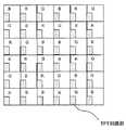
有機エレクトロルミネッセンス素子や液晶のドットマトリックスディスプレイはその画素の配列から大きく4種類に分けられており、それぞれストライプ配列(図1)、デルタ配列(図2)、ダイアゴナル(モザイク)配列(図3)、レクタングル(矩形)配列(図4)と呼ばれている。そのなかでも一般には、主にストライプ配列とデルタ配列が用いられている。各画素を交点とする規則的な格子を考えた場合に、ストライプ配列はその単位格子が四角形になっており、デルタ配列はその単位格子が三角形状になっている。ストライプ配列のドットマトリクスディスプレイは文字や罫線の表示に適しており、液晶ディスプレイではパソコン用モニタや携帯電話のディスプレイなどに広く用いられている。一方、図2に示すようなデルタ配列になる有機エレクトロルミネッセンス素子を用いたディスプレイは画像の表示に適しており、デジタルカメラやデジタルビデオカメラのビューアなどに用いられている。 Organic electroluminescence elements and liquid crystal dot matrix displays are roughly divided into four types according to their pixel arrangements: stripe arrangement (Fig. 1), delta arrangement (Fig. 2), diagonal (mosaic) arrangement (Fig. 3), It is called a rectangle (rectangular) array (FIG. 4). Among them, in general, a stripe arrangement and a delta arrangement are mainly used. When considering a regular grid with each pixel as an intersection, the stripe arrangement has a square unit cell, and the delta arrangement has a triangular unit cell. A dot matrix display with a stripe arrangement is suitable for displaying characters and ruled lines, and a liquid crystal display is widely used for monitors for personal computers and displays for mobile phones. On the other hand, a display using an organic electroluminescence element having a delta arrangement as shown in FIG. 2 is suitable for displaying an image, and is used for a viewer of a digital camera or a digital video camera.
図5は、凸版印刷法によって発光部を形成するための印刷工程の一例を図示したものである。図5中に示すインキパン101には有機発光材料などを溶媒に溶解あるいは分散させてなるインキが貯留されている。アニロックスロール103にはこのインキパン101中においてインキが供給された後に、その上の余分なインキがドクター102によって掻き落とされ、孔内部にのみインキが蓄えられる。孔内部のインキは、アニロックスロール103と相対して回転する版胴105に巻かれている凸版104の画像形成部上に転移させられ、そこにパターン化されたインキの薄膜を形成する。さらに、画像形成部上に形成されたパターン化された薄膜は版胴105と相対して移動する基板106上に転移させられ、その上の発光部の形成個所に所望の発光部が形成される。 FIG. 5 illustrates an example of a printing process for forming a light emitting portion by a relief printing method. Ink
有機エレクトロルミネッセンス素子を印刷法で作製する場合、発光部を形成するための印刷版における画像形成部のパターンは、有機エレクトロルミネッセンス素子の各画素を構成する複数の発光部のうち、同一の発光色で発光する発光部を形成するための画像形成部が複数配列された構成となっており、このような印刷版を発光色の色数分用意し、それぞれの発光色に発光する発光部を順次印刷していくことで有機発光層を得ている。 When an organic electroluminescent element is produced by a printing method, the pattern of the image forming portion in the printing plate for forming the light emitting portion is the same emission color among the plurality of light emitting portions constituting each pixel of the organic electroluminescent element. A plurality of image forming units for forming light emitting units that emit light are arranged, and such printing plates are prepared for the number of colors of light emission, and the light emitting units that emit light of each light emission color are sequentially arranged. The organic light emitting layer is obtained by printing.
図6は、発光色が異なる3種の発光部から構成される三角形状の画素を単位格子(「三角形状の画素」とはサブピクセル1つ1つの形が三角形であるということを意味していない)としてそれらがデルタ配列されている有機エレクトロルミネッセンス素子における画素の配列状態を示す説明図である。 FIG. 6 shows a unit pixel (“triangular pixel” means that each of the sub-pixels is a triangle. It is explanatory drawing which shows the arrangement | sequence state of the pixel in the organic electroluminescent element in which they are delta-arranged.
一方、図7は、図6に示すような構成の有機エレクトロルミネッセンス素子中の1つの画素内における発光色が異なる3種の発光部の配列状態の一例を示している。41、42、43はそれぞれ発光部(青、緑、赤のいずれか)、7は隔壁部分に相当する。 On the other hand, FIG. 7 shows an example of an arrangement state of three types of light emitting units having different emission colors in one pixel in the organic electroluminescence element having the configuration shown in FIG.
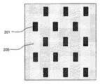
一方、図8及び図9は、図6に示すようなデルタ配列になる有機エレクトロルミネッセンス素子の発光部を、本発明に係る製造方法において形成するときに使用される印刷版205の一例を模式的に示している。図8が印刷版205の表面部分におけるドット状の凸部パターン201の形成状況を、図9が図8に示す印刷版の概略の断面構成をそれぞれ示している。 On the other hand, FIG. 8 and FIG. 9 schematically show an example of the
例えば上記印刷法を用いて、図8に示すような印刷版によって、図6に示すような有機エレクトロルミネッセンス素子を印刷する場合、印刷版の画素パターンが単位画素ごとにドット状に独立しているために、版凸部の接触するアニロックスロールのセル目位置によって版に供給されるインキ量が異なること、さらに複数画素がつながったパターンと異なり版凸部上でのインキ流動が出来ないことなどがおこる。それによって転写される膜厚が被転写部ごとに不均一になり、発光ムラや発光色度ズレが引き起されるなどの問題がある。 For example, when the organic electroluminescence element as shown in FIG. 6 is printed with the printing plate as shown in FIG. 8 using the above printing method, the pixel pattern of the printing plate is independent in the form of dots for each unit pixel. For this reason, the amount of ink supplied to the plate varies depending on the cell position of the anilox roll that the plate convex portion contacts, and the ink flow on the plate convex portion cannot be performed unlike a pattern in which a plurality of pixels are connected. It happens. As a result, the film thickness to be transferred becomes non-uniform for each transferred portion, causing problems such as uneven light emission and light emission chromaticity deviation.
本発明は上述のような問題を解決するためになされたものであり、その目的はデルタ配列のような、一般にドット状パターンを用いた印刷法によって有機エレクトロルミネッセンス素子の発光部を作製する際に、画素内の膜厚の不均一による影響を少なくして発光部を形成することができ、発光ムラや発光色度ズレを極力抑えた有機エレクトロルミネッセンス素子を提供できるようにした印刷用凸版及びその印刷用凸版を用いた電子デバイスの製造方法並びに有機エレクトロルミネッセンス素子を提供することにある。 The present invention has been made to solve the above-described problems, and its purpose is to produce a light emitting portion of an organic electroluminescence element by a printing method using a dot pattern, such as a delta arrangement. A printing relief printing plate capable of providing an organic electroluminescence device capable of forming a light emitting portion with reduced influence of non-uniform film thickness within a pixel and suppressing light emission unevenness and light emission chromaticity deviation as much as possible An object of the present invention is to provide a method for producing an electronic device using a relief printing plate and an organic electroluminescence element.
以上のような課題を解決するためになされたもので、請求項1記載の発明は、基板上に基板上にデルタ配列、ダイアゴナル配列及びレクタングル配列の何れかのパターン配列で形成された複数の凸部を有し、該各凸部の突出方向の先端が、有機電子材料を主成分として含むインキが塗布される接触面として形成され、前記接触面に塗布された前記インキを凸版印刷法によって被転写基板に転写することで前記被転写基板上に被転写部を形成する印刷用凸版であって、前記凸部の形成箇所を除く前記基板上の箇所に前記各凸部と連結された凸状の接続部が形成され、前記接続部は、前記各凸部の前記接触面と同一高さでかつ前記接触面と接続された面を有していることを特徴とする印刷用凸版である。Which has been made to solve the above problems, a first aspect of the present invention,a delta arrangement on a substrate on a substrate, a plurality of convexformed in any of pattern arrangement diagonal arrangement and rectangle arrangement has a section, the tip of the projecting direction ofthe respective convex sections is formed as a contact surface for the ink containing the organic electronic material as a main component is applied, the ink applied to the contact surface by a relief printing method A printing relief plate for forming a transferred portion on the transferred substrate by transferring to a transfer substrate, wherein the protruding portionis connected toeach protruding portion ata position on the substrate excluding the forming portion ofthe protruding portion. The connecting portionis a relief printing plate characterizedin that the connecting portion has the sameheight as the contact surfaceof each convex portionand a surface connected to the contact surface .
請求項2の発明は、前記複数の凸部は、1方向に間隔をおいて並べられて凸部列を形成しており、前記凸部列は前記1方向と直交する方向に間隔をおいて複数設けられ、前記接続部は、前記凸部列の長手方向に延在し該凸部列を接続していることを特徴とする請求項1記載の印刷用凸版である。According to asecond aspect of the present invention, the plurality of convex portions are arranged in one direction at intervals to form a convex portion row, and the convex portion row is spaced in a direction orthogonal to the one direction. 2. The relief printing plate according to
請求項3の発明は、前記複数の凸部は、1方向に間隔をおいて並べられて凸部列を形成しており、前記凸部列は前記1方向と直交する方向に間隔をおいて複数設けられ、前記接続部は、前記凸部列の長手方向に延在し隣り合う2つの凸部列を接続していることを特徴とする請求項1記載の印刷用凸版である。According to athird aspect of the present invention, the plurality of convex portions are arranged in one direction at intervals to form a convex portion row, and the convex portion row is spaced in a direction orthogonal to the one direction. 2. The relief printing plate according to
請求項4の発明は、前記複数の凸部は、1方向に間隔をおいて並べられて凸部列を形成しており、前記凸部列は前記1方向と直交する方向に間隔をおいて複数設けられ、前記隣り合う凸部列は、前記1方向と直交する方向において前記凸部の位相がずらされており、前記接続部は、前記凸部列の長手方向に前記位相がずらされた分延在し隣り合う前記凸部列の位相がずらされた前記凸部同士を接続していることを特徴とする請求項1記載の印刷用凸版である。According to afourth aspect of the present invention, the plurality of convex portions are arranged in one direction at intervals to form a convex portion row, and the convex portion row is spaced in a direction orthogonal to the one direction. A plurality of the adjacent protrusion rows are shifted in phase in the direction perpendicular to the one direction, and the phase of the connection portion is shifted in the longitudinal direction of the protrusion row. 2. The relief printing plate according to
請求項5の発明は、請求項1から4の何れか1項に記載の印刷用凸版を用い、該凸版にインキを供給する工程と、塗工液を被転写体に転写する工程とを有することを特徴とする電子デバイスの製造方法である。Invention of
請求項6の発明は、前記電子デバイスが有機エレクトロルミネッセンス素子であることを特徴とする請求項5記載の電子デバイスの製造方法である。The invention of claim6 is the method of manufacturing an electronic device according to
請求項7の発明は、請求項5または6記載の電子デバイスの製造方法により作製されることを特徴とする有機エレクトロルミネッセンス素子である。Aseventh aspect of the invention is an organic electroluminescence element produced by the method of manufacturing an electronic device according to thefifth orsixth aspect.
本発明によれば、インキが塗布される凸部の形成箇所を除く基板上の箇所に各凸部と連結された凸状の接続部が形成され、この接続部は、各凸部の接触面と同一高さでかつ接触面と接続された面を有する構成にした。
したがって、凸部の接触面に転写されたインキの流動を接続部を介して可能にし、それによって凸部上のインキ量の不均一性を緩和でき、画素ごとの膜厚均一性が向上し、それによって膜厚の不均一に由来する発光効率の低下や発光色度のズレを防ぐことが可能となる。According to the present invention,a convex connection portionconnected to each convex portion is formed ata location on the substrate excluding a location where the convex portion to which ink is appliedis formed, and this connection portion is a contact surface of each convex portion. And having a surface connected to the contact surface .
Therefore, it is possible to flow the ink transferred to the contact surface of the convex portion through the connecting portion, thereby reducing the non-uniformity of the ink amount on the convex portion, improving the film thickness uniformity for each pixel, As a result, it is possible to prevent a decrease in light emission efficiency and a shift in light emission chromaticity due to non-uniform film thickness.
以下、この発明の実施の形態を図面に基づいて説明する。なお、本発明はこれに限るものではない。Hereinafter, embodiments of the present invention will be described with reference to the drawings. The present invention is not limited to this.
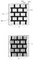
図10に本発明の印刷用凸版の一例の説明断面図を示した。図10(a)、図10(b)ともに基材200上に反射防止層202、樹脂層により形成される複数の凸部からなる凸部パターン201が形成されている。図10(a)では、凸部パターンは、複数の凸部が連続して基材上に形成されることで構成されている。図10(b)では、凸部パターンは、複数の凸部がそれぞれ切り離されて独立して基材上に形成されることで構成されている。本発明では、図10(a)、図10(b)どちらの印刷用凸版を用いても構わない。なお、必要に応じて樹脂層と基材層との間に紫外線反射防止効果、耐水性、耐油性、撥水性、接着性などを付与するための層を加えても良い。 FIG. 10 shows an explanatory sectional view of an example of the relief printing plate of the present invention. 10A and 10B, a
本発明の印刷用凸版に用いられる版材において、凸部パターンが形成される基材としては、印刷に対する機械的強度を有すれば良く、ポリエチレン、ポリスチレン、ポリブタジエン、ポリ塩化ビニル、ポリ塩化ビニリデン、ポリ酢酸ビニル、ポリアミド、ポリエーテルスルホン、ポリエチレンテレフタレート、ポリエチレンナフタレート、ポリエーテルスルホン、ポリビニルアルコールなどの公知の合成樹脂、鉄や銅、アルミニウムといった公知の金属、またはそれらの積層体を用いることができる。 In the plate material used for the relief printing plate of the present invention, the substrate on which the projection pattern is formed is only required to have mechanical strength against printing, such as polyethylene, polystyrene, polybutadiene, polyvinyl chloride, polyvinylidene chloride, Known synthetic resins such as polyvinyl acetate, polyamide, polyethersulfone, polyethylene terephthalate, polyethylene naphthalate, polyethersulfone, and polyvinyl alcohol, known metals such as iron, copper, and aluminum, or laminates thereof can be used. .
なお、本発明に使用する印刷用凸版を構成する基材200としては、高い寸法安定性を保持するものが望ましい。従って、基材として用いられる材料としては金属が好適に使用される。基材200として用いられる金属としては鉄、アルミニウム、銅、亜鉛、ニッケル、チタン、クロム、金、銀やそれらの合金、積層体などが挙げられるが、特に、加工性、経済性から鉄を主成分とするスチール基材やアルミ基材を好適に用いることができる。 In addition, as the
凸版の凸部を形成する樹脂の一成分となるポリマーは、ニトリルゴム、シリコーンゴム、イソプレンゴム、スチレンブタジエンゴム、ブタジエンゴム、クロロプレンゴム、ブチルゴム、アクリロニトリルゴム、エチレンプロピレンゴム、ウレタンゴムなどのゴムの他に、ポリエチレン、ポリスチレン、ポリブタジエン、ポリ塩化ビニル、ポリ塩化ビニリデン、ポリ酢酸ビニル、ポリアミド、ポリウレタン、ポリエーテルスルホン、ポリエチレンテレフタレート、ポリエチレンナフタレート、ポリエーテルスルホン、ポリビニルアルコールなどの合成樹脂やそれらの共重合体、セルロースなどの天然高分子などから一種類以上を選択することができるが、有機発光材料などといった塗工液を塗布する場合、有機溶剤に対する耐溶剤性の観点から、フッ素系エラストマーやポリ四フッ化エチレン、ポリフッ化ビニリデン、ポリ六フッ化ビニリデンやそれらの共重合体といったフッ素系樹脂が望ましい。 The polymer that is one component of the resin that forms the convex part of the relief plate is made of nitrile rubber, silicone rubber, isoprene rubber, styrene butadiene rubber, butadiene rubber, chloroprene rubber, butyl rubber, acrylonitrile rubber, ethylene propylene rubber, urethane rubber, etc. In addition, synthetic resins such as polyethylene, polystyrene, polybutadiene, polyvinyl chloride, polyvinylidene chloride, polyvinyl acetate, polyamide, polyurethane, polyethersulfone, polyethylene terephthalate, polyethylene naphthalate, polyethersulfone, and polyvinyl alcohol, and their co-polymers. One or more types can be selected from polymers, natural polymers such as cellulose, etc., but when applying coating liquids such as organic light emitting materials, from the viewpoint of solvent resistance to organic solvents Fluorine-based elastomer or polytetrafluoroethylene, polyvinylidene fluoride, fluorine-based resins such as polyethylene hexafluoride vinylidene and copolymers thereof are preferred.
また、少なくとも、ポリビニルアルコール、ポリアミド、ポリウレタン、酢酸セルロースコハク酸エステル、部分ケン化ポリ酢酸ビニル、カチオン型ピペラジン含有ポリアミドやこれらの誘導体といった水溶性溶剤に可溶なものを一種類以上含有することによっても耐溶剤性を付与することが可能となるため、これらの内から一つ以上を選択し用いることも望ましい。 In addition, by containing at least one kind soluble in water-soluble solvents such as polyvinyl alcohol, polyamide, polyurethane, cellulose acetate succinate, partially saponified polyvinyl acetate, cationic piperazine-containing polyamide and derivatives thereof Since it is possible to impart solvent resistance, it is also desirable to select and use one or more of these.
反射抑制層としては、測定装置の一般的な観察光である波長領域が400nmから800nm付近の白色光に対する反射抑制効果があれば良く、光拡散による方法と光吸収による方法のどちらを用いても良いが、光拡散を用いた場合、エッジ検出の際、拡散光の影響によりコントラストが低くなり測定精度が落ち易くなる。この理由から反射抑制層としては光の吸収層を用いることが最も望ましい。 The reflection suppressing layer only needs to have a reflection suppressing effect on white light having a wavelength range of 400 nm to 800 nm, which is a general observation light of the measuring apparatus, and either a light diffusion method or a light absorption method is used. However, when light diffusion is used, the contrast is lowered due to the influence of the diffused light and the measurement accuracy is liable to be lowered during edge detection. For this reason, it is most desirable to use a light absorption layer as the reflection suppressing layer.
本発明における樹脂層による凸部は、ポジ型感光性樹脂を用いたフォトリソグラフィー法、ネガ型感光性樹脂を用いたフォトリソグラフィー法、射出成型、凸版印刷法、凹版印刷法、平版印刷法、孔版印刷法、レーザーアブレーション法等の種々のパターン成型法を用いることができるが、パターンの高精細さの観点から、感光性樹脂を用いたフォトリソグラフィー法が望ましく、また、要求精度の凸版を形成可能なネガ型感光性樹脂を用いたフォトリソグラフィー法が最も望ましい。 The convex portion by the resin layer in the present invention is a photolithography method using a positive photosensitive resin, a photolithography method using a negative photosensitive resin, injection molding, a relief printing method, an intaglio printing method, a lithographic printing method, a stencil printing plate. Various pattern molding methods such as printing method and laser ablation method can be used, but from the viewpoint of high-definition of pattern, photolithography method using photosensitive resin is desirable, and relief printing with required accuracy can be formed A photolithography method using a negative photosensitive resin is most desirable.
感光光性樹脂を用いたフォトリソグラフィー法を凸部パターン形成法として適用する場合、基材層、反射抑制層、感光性樹脂層が順次積層されている板状感光性樹脂積層体から凸版の凸部を形成することが最も望ましい。感光性樹脂層の成型方法は、射出成型法、突出成型法、ラミネート法、バーコート法、スリットコート法、カンマコート法などの公知の方法を用いることができる。 When a photolithographic method using a photosensitive resin is applied as a convex pattern forming method, a relief of a relief plate from a plate-shaped photosensitive resin laminate in which a base material layer, an antireflection layer, and a photosensitive resin layer are sequentially laminated. It is most desirable to form the part. As a method for molding the photosensitive resin layer, a known method such as an injection molding method, a protruding molding method, a laminating method, a bar coating method, a slit coating method, or a comma coating method can be used.
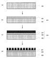
図11に本発明における板状感光性樹脂積層体の成型方法を示した。まず基材200にバーコート法、スリットコート法、スプレーコート法、フレキソ印刷、グラビア印刷などのウェットコーティング法もしくはスパッタ法、真空蒸着法、CVD法などのドライコーティング法により反射抑制層202を成膜し、積層体203とする(図11(a)、(b))。次に積層体203に感光性樹脂層201´を射出成型法、突出成型法、ラミネート法、バーコート法、スリットコート法、カンマコート法などの公知の方法で成膜し積層体204とする(図11(c))。この積層体204に対し、公知の露光、現像の工程を経て、目的とするパターン形成用凸版を形成する(図11(d))。 FIG. 11 shows a method for molding a plate-like photosensitive resin laminate in the present invention. First, the
次に、本発明によって作製される印刷用凸版のパターン形状について述べる。 Next, the pattern shape of the relief printing plate produced by the present invention will be described.
凸版印刷法によって有機エレクトロルミネッセンス素子を印刷する場合、有機エレクトロルミネッセンス表示素子の画素領域に対応して印刷用凸版の凸部を形成する必要があり、画素パターンによって印刷用凸版のパターンも大きく左右される。 When printing an organic electroluminescent element by the relief printing method, it is necessary to form the convex part of the printing relief plate corresponding to the pixel region of the organic electroluminescence display element, and the pattern of the relief printing plate greatly depends on the pixel pattern. The
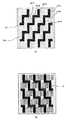
例えば、図6に示すようなデルタ配列の有機エレクトロルミネッセンス素子を凸版印刷法によって作製する場合には、一般に図8に示すような画素パターンと対応したドット状のパターンの凸版が用いられる。言い換えると、各発光部41、42、43のそれぞれと対応する複数の凸部からなる凸部パターン201を有する凸版が用いられる。
しかしながら、印刷版の画素パターンが単位画素ごとにドット状に独立しているために、ドット状パターンでは版凸部の接触するアニロックスロールのセル目位置によって版に供給されるインキ量が異なること、さらに複数画素がつながったパターンと異なり版凸部上でのインキ流動が出来ないことなどがおこる。それによって画素内に転写される膜厚が被転写ごとに異なることになり、発光ムラの発生や発光色度ズレが引き起されるなどの問題が生じやすい。
言い換えると、各凸部の突出方向の先端に形成された、有機電子材料を主成分として含むインキが塗布される接触面が切り離されて分離されているために、各接触面が接触するアニロックスロールのセル目位置によって各接触面に供給されるインキ量が異なり、さらに各接触面上でのインキ流動が出来ない。それによって各接触面によって転写される膜厚が接触面ごとに異なることになり、発光ムラの発生や発光色度ズレが引き起されるなどの問題が生じやすい。For example, when an organic electroluminescence element having a delta arrangement as shown in FIG. 6 is manufactured by a relief printing method, a relief pattern having a dot pattern corresponding to the pixel pattern as shown in FIG. 8 is generally used. In other words, a relief plate having a
However, since the pixel pattern of the printing plate is independent in a dot shape for each unit pixel, the amount of ink supplied to the plate varies depending on the cell position of the anilox roll in contact with the plate convex portion in the dot pattern, Furthermore, unlike a pattern in which a plurality of pixels are connected, ink flow on the plate convex portion cannot be performed. As a result, the thickness of the film transferred into the pixel varies from one transfer to another, and problems such as the occurrence of uneven light emission and a shift in light emission chromaticity are likely to occur.
In other words, an anilox roll that is formed at the tip in the projecting direction of each convex portion and that is contacted with each contact surface because the contact surface to which ink containing an organic electronic material as a main component is applied is separated and separated. The amount of ink supplied to each contact surface differs depending on the position of each cell, and ink flow on each contact surface is not possible. As a result, the film thickness transferred by each contact surface varies from contact surface to contact surface, and problems such as occurrence of uneven light emission and displacement of light emission chromaticity are likely to occur.
そこで本発明では、印刷版の凸部パターンに画素ごとのドットを非画素部においてつなげることによって、アニロックスロールから版凸部上に転写されたインキの流動を版凸部上で可能にし、それによって版凸部上のインキ量の不均一性を緩和した。
言い換えると、凸部の形成箇所を除く基板上の箇所に各凸部と連結された凸状の接続部を形成し、この接続部は、各凸部の接触面と同一高さでかつ接触面と接続された面を有していることによって、アニロックスロールから版凸部上に転写されたインキの流動を版凸部上で可能にし、それによって版凸部上のインキ量の不均一性を緩和した。Therefore, in the present invention, by connecting dots for each pixel to the convex pattern of the printing plate in the non-pixel part, the flow of the ink transferred from the anilox roll onto the convex part of the plate is enabled on the convex part of the plate, thereby The unevenness of the ink amount on the plate convex part was eased.
In other words, a convexconnecting portion connected to each convex portion is formed at a location on the substrate excluding the location where the convex portion is formed, and this connecting portion has the same height as the contact surface of each convex portion and the contact surface. The surface transferred to the plate convex portion from the anilox roll enables the flow of the ink on the plate convex portion, thereby reducing the non-uniformity of the ink amount on the plate convex portion. Relaxed.
本発明の一例として、図6に示すようなデルタ配列の有機エレクトロルミネッセンス素子に対して、図12(a)、図13(a)、図14(a)に示すような凸部パターンの凸版を作製した。この版を用いて1色だけ印刷を行うことによって、それぞれ図12(b)、図13(b)、図14(b)に示すような状態の有機エレクトロルミネッセンス素子が得られる。なお、本発明によるパターン形状についてはこれだけに限るものではない。 As an example of the present invention, a relief plate having a convex pattern as shown in FIGS. 12 (a), 13 (a), and 14 (a) is applied to an organic electroluminescence element having a delta arrangement as shown in FIG. Produced. By printing only one color using this plate, organic electroluminescence elements in the states as shown in FIGS. 12B, 13B, and 14B are obtained. The pattern shape according to the present invention is not limited to this.
より詳細に説明する。
図12(a)に示す印刷用凸版では、複数の凸部201Aは、1方向に間隔をおいて並べられて凸部列を形成している。
凸部列は1方向と直交する方向に間隔をおいて複数設けられている。
接続部201Bは、凸部列の長手方向に延在し該凸部列を接続している。
図13(a)に示す印刷用凸版では、複数の凸部201Aは、1方向に間隔をおいて並べられて凸部列を形成している。
凸部列は1方向と直交する方向に間隔をおいて複数設けられている。
接続部201Bは、凸部列の長手方向に延在し隣り合う2つの凸部列を接続している。
図14(a)に示す印刷用凸版では、複数の凸部201Aは、1方向に間隔をおいて並べられて凸部列を形成している。
凸部列は1方向と直交する方向に間隔をおいて複数設けられている。
隣り合う凸部列は、1方向と直交する方向において凸部201Aの位相がずらされている。
接続部201Bは、凸部列の長手方向に位相がずらされた分延在し隣り合う凸部列の位相がずらされた凸部201A同士を接続している。This will be described in more detail.
In the printing relief printing shown in FIG. 12A, a plurality of
A plurality of convex portion rows are provided at intervals in a direction orthogonal to one direction.
The connecting portion 201B extends in the longitudinal direction of the convex portion row and connects the convex portion row.
In the printing relief printing shown in FIG. 13A, a plurality of
A plurality of convex portion rows are provided at intervals in a direction orthogonal to one direction.
The connecting portion 201B extends in the longitudinal direction of the convex portion row and connects two adjacent convex portion rows.
In the relief printing plate shown in FIG. 14A, the plurality of
A plurality of convex portion rows are provided at intervals in a direction orthogonal to one direction.
Adjacent protrusion rows are shifted in phase in the
The connecting portion 201B extends by a phase shifted in the longitudinal direction of the convex row, and connects the
図12(b)、図13(b)、図14(b)からも明らかであるが、本発明の特徴である版における凸部201Aの接触面と同一面を有し複数の凸部201Aを接続する接続部201Bによって基材200上に転写された被転写部は非発光部であるため、複数色のインキで続けて印刷を行うことによって起こるインキの混色は、発光に影響を及ぼさない。 As is clear from FIGS. 12B, 13B, and 14B, a plurality of
また、これらの効果は、印刷用凸版によって形成される各発光部の配列がデルタ配列である場合に限定されず、ダイアゴナル配列やレクタングル配列など一般にドット状パターンによって印刷される全ての画素パターンに対し有効である。
すなわち、本発明は、印刷用凸版の凸部201Aのパターンがデルタ配列であるものに限定されず、凸部201Aのパターンがダイアゴナル配列やレクタングル配列など一般的な配列である印刷用凸版に適用されることは無論である。In addition, these effects are not limited to the case where the arrangement of the light emitting portions formed by the printing relief plate is a delta arrangement, but for all pixel patterns that are generally printed in a dot pattern such as a diagonal arrangement or a rectangle arrangement. It is valid.
That is, the present invention is not limited to the pattern of the
次に、本発明によりパターン形成された凸版を用いた回路パターンの製造方法の一例として、有機EL素子の作製方法について説明する。なお、本発明はこれに限るものではない。 Next, a method for producing an organic EL element will be described as an example of a method for producing a circuit pattern using a relief pattern patterned according to the present invention. The present invention is not limited to this.
図5に本発明の印刷物の製造に用いられる凸版印刷装置の概略図を示した。ステージ107には被印刷基板106が固定されており、本発明によってパターン形成された印刷用凸版104は版胴105に固定され、印刷用凸版104はインキ供給体であるアニロックスロール103と接しており、アニロックスロール103はインキ補充装置101とドクター102を備えている。 FIG. 5 shows a schematic diagram of a relief printing apparatus used for producing the printed matter of the present invention. A
まず、インキ補充装置101からアニロックスロール103へインキを補充し、アニロックスロール103に供給されたインキ108のうち余分なインキは、ドクター102により除去される。インキ補充装置101には、滴下型のインキ補充装置、ファウンテンロール、スリットコータ、ダイコータ、キャップコータなどのコータやそれらを組み合わせたものなどを用いることもできる。ドクター102にはドクターブレードの他にドクターロールといった公知の物を用いることもできる。また、アニロックスロール103は、クロム製やセラミックス製のものを用いることができる。また、印刷用凸版へのインキ供給体としてシリンダー状のアニロックスロールではなく、平版のアニロックス版を用いることも可能である。平版のアニロックス版は、例えば、図5の被印刷基板106の位置に配置され、インキ補充装置によりアニロックス版全面にインキを補充した後、版胴を回転させることにより被印刷基板へのインキの供給をおこなうことができる。 First, ink is replenished from the
印刷用凸版へのインキ供給体であるアニロックスロール103表面にドクターによって均一に保持されたインキは、版胴105に取り付けられた印刷用凸版104の凸部パターンに転移、供給される。そして、版胴105の回転に合わせて印刷用凸版104の凸部パターンと基板は接しながら相対的に移動し、インキ108はステージ107上にある被印刷基板106の所定位置に転移し被印刷基板にインキパターン108aを形成する。被印刷基板にインキパターンが設けられた後は、必要に応じてオーブンなどによる乾燥工程を設けることができる。 The ink uniformly held by the doctor on the surface of the
なお、印刷用凸版上にあるインキを被印刷基板に印刷するときにおいては、版胴105の回転にあわせ被印刷基板106が固定されたステージ17を移動させる方式であってもよいし、図5上部の版胴105、印刷用凸版104、アニロックスロール103、インキ補充装置101からなる印刷ユニットを版胴の回転に合わせ移動させる方式であってもよい。また、本発明の印刷用凸版は版胴105上に樹脂層を形成し、直接製版し、凸部パターンを形成してもよい。 When printing the ink on the printing relief plate on the printing substrate, the stage 17 to which the
なお、図5は1枚毎に被印刷基板にインキパターンを形成する枚葉式の凸版印刷装置であるが、本発明の印刷物の製造方法にあって被印刷基板がウェブ状で巻き取り可能である場合には、ロール・トゥー・ロール方式の凸版印刷装置を用いることもできる。ロール・トゥー・ロール方式の凸版印刷装置を用いた場合には連続してインキパターンを形成することが可能となり、製造コストを低くすることが可能となる。 Note that FIG. 5 shows a sheet-fed relief printing apparatus that forms an ink pattern on a substrate to be printed one by one. However, in the method for producing a printed material according to the present invention, the substrate to be printed can be wound in a web shape. In some cases, a roll-to-roll relief printing apparatus can also be used. In the case of using a roll-to-roll letterpress printing apparatus, it is possible to continuously form an ink pattern and to reduce the manufacturing cost.
次に、本発明によってパターン形成した印刷用凸版を用いた印刷物の製造方法の一例として、有機EL素子の製造方法について説明する。なお、本発明はこれに限るものではない。図15に本発明の有機EL素子の説明断面図を示した。有機EL素子の駆動方法としては、パッシブマトリックス方式とアクティブマトリックス方式があるが、本発明の有機EL素子はパッシブマトリックス方式の有機EL素子、アクティブマトリックス方式の有機EL素子のどちらにも適用可能である。 Next, a method for producing an organic EL element will be described as an example of a method for producing a printed material using a relief printing plate patterned according to the present invention. The present invention is not limited to this. FIG. 15 shows an explanatory cross-sectional view of the organic EL element of the present invention. There are a passive matrix type and an active matrix type as a driving method of the organic EL element, but the organic EL element of the present invention can be applied to either a passive matrix type organic EL element or an active matrix type organic EL element. .
パッシブマトリックス方式とはストライプ状の電極を直交させるように対向させ、その交点を発光させる方式であるのに対し、アクティブマトリックス方式は画素毎にトランジスタを形成した、いわゆる薄膜トランジスタ(TFT)基板を用いることにより、画素毎に独立して発光する方式である。 The passive matrix method is a method in which stripe-shaped electrodes are opposed to each other so as to be orthogonal to each other, and light is emitted at the intersection, whereas the active matrix method uses a so-called thin film transistor (TFT) substrate in which a transistor is formed for each pixel. Thus, the light is emitted independently for each pixel.
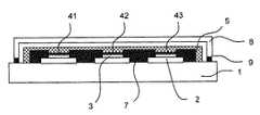
図14に示すように、本発明の有機EL素子は、基板1の上に、陽極としてストライプ状に第一電極2を有している。隔壁7は第一電極2間に設けられ、第一電極2端部のバリ等よるショートを防ぐことを目的として第一電極2端部を覆うことがましい。 As shown in FIG. 14, the organic EL element of the present invention has a
そして、本発明の有機EL素子は、第一電極2上であって、隔壁7で区画された領域(発光領域、画素部)に有機発光層及び発光補助層からなる有機EL層を有している。電極間に挟まれる有機EL層は、有機発光層単独から構成されたものであってもよいし、有機発光層と発光補助層との積層構造から構成されたものでもよい。発光補助層としては正孔輸送層、正孔注入層、電子輸送層、電子注入層、電荷発生層が挙げられる。図14では発光補助層である正孔輸送層3と有機発光層(41、42、43)との積層構造からなる構成を示している。第一電極2上に正孔輸送層3が設けられ、正孔輸送層3上に赤色(R)有機発光層41、緑色(G)有機発光層42、青色(B)有機発光層43がそれぞれ設けられている。 And the organic EL element of this invention has the organic EL layer which consists of an organic light emitting layer and a light emission auxiliary layer in the area | region (light emission area | region, pixel part) on the
次に、有機発光層上に陽極である第一電極2と対向するように陰極として第二電極5が配置される。パッシブマトリックス方式の場合、ストライプ状を有する第一電極と直交する形で第二電極はストライプ状に設けられる。アクティブマトリックス方式の場合、第二電極は、有機EL素子全面に形成される。更に、環境中の水分、酸素の第一電極、有機発光層、発光補助層、第二電極への侵入を防ぐために有効画素全面に対してガラスキャップ8等による封止体が設けられ、接着剤9を介して基板1と貼りあわされる。 Next, the
本発明の有機EL素子は、少なくとも基板と、当該基板に支持されたパターン状の第一電極と、有機発光層と、第二電極を具備する。本発明の有機EL素子は、図14とは逆に、第一電極を陰極、第二電極を陽極とする構造であっても良い。また、ガラスキャップ等の封止体の代わりに有機発光媒体層や電極を外部の酸素や水分の浸入から保護するためにパッシベーション層や外部応力から保護する保護層、あるいはその両方の機能備えた封止基材を備えてもよい。 The organic EL device of the present invention includes at least a substrate, a patterned first electrode supported by the substrate, an organic light emitting layer, and a second electrode. Contrary to FIG. 14, the organic EL element of the present invention may have a structure in which the first electrode is a cathode and the second electrode is an anode. In addition, in order to protect the organic light emitting medium layer and the electrode from the ingress of external oxygen and moisture in place of a sealing body such as a glass cap, a sealing layer having a function of a passivation layer and a protective layer for protecting from external stress, or both, is provided. You may provide a stop base material.
次に、有機EL素子の製造方法を説明する。 Next, the manufacturing method of an organic EL element is demonstrated.
本発明にかかる基板としては、絶縁性を有する基板であればいかなる基板も使用することができる。この基板側から光を取り出すボトムエミッション方式の有機EL素子とする場合には、基板として透明なものを使用する必要がある。 As the substrate according to the present invention, any substrate can be used as long as it has an insulating property. In the case of a bottom emission type organic EL element that extracts light from the substrate side, it is necessary to use a transparent substrate.
例えば、基板としてはガラス基板や石英基板が使用できる。また、ポリプロピレン、ポリエーテルサルフォン、ポリカーボネート、シクロオレフィンポリマー、ポリアクリレート、ポリアミド、ポリメチルメタクリレート、ポリエチレンテレフタレート、ポリエチレンナフタレート等のプラスチックフィルムやシートであっても良い。これら、プラスチックフィルムやシートに、有機発光媒体層への水分の侵入を防ぐことを目的として、金属酸化物薄膜、金属弗化物薄膜、金属窒化物薄膜、金属酸窒化膜薄膜、あるいは高分子樹脂膜を積層したものを基板として利用してもよい。 For example, a glass substrate or a quartz substrate can be used as the substrate. Further, it may be a plastic film or sheet such as polypropylene, polyethersulfone, polycarbonate, cycloolefin polymer, polyacrylate, polyamide, polymethyl methacrylate, polyethylene terephthalate, or polyethylene naphthalate. Metal oxide thin film, metal fluoride thin film, metal nitride thin film, metal oxynitride thin film, or polymer resin film for the purpose of preventing moisture from entering the organic light emitting medium layer in these plastic films and sheets You may utilize what laminated | stacked these as a board | substrate.
また、これらの基板は、あらかじめ加熱処理を行うことにより、基板内部や表面に吸着した水分を極力低減することがより好ましい。また、基板上に積層される材料に応じて、密着性を向上させるために、超音波洗浄処理、コロナ放電処理、プラズマ処理、UVオゾン処理などの表面処理を施してから使用することが好ましい。 In addition, it is more preferable to reduce the moisture adsorbed on the inside or the surface of the substrate as much as possible by performing a heat treatment on these substrates in advance. Further, in order to improve the adhesion depending on the material to be laminated on the substrate, it is preferable to use after performing surface treatment such as ultrasonic cleaning treatment, corona discharge treatment, plasma treatment, UV ozone treatment.
また、これらに薄膜トランジスタ(TFT)を形成して、アクティブマトリックス方式の有機EL素子用の基板とすることが可能である。本発明のアクティブマトリックス方式の基板の一例の説明断面図を図16に示す。本発明の有機EL素子基板とする場合には、TFT120上に、平坦化層117が形成してあるとともに、平坦化層117上に有機EL素子の下部電極(第一電極2)が設けられており、かつ、TFTと下部電極とが平坦化層117に設けたコンタクトホール118を介して電気接続してあることが好ましい。このように構成することにより、TFTと、有機EL素子との間で、優れた電気絶縁性を得ることができる。 Further, a thin film transistor (TFT) can be formed on these to form a substrate for an active matrix organic EL element. FIG. 16 shows an explanatory cross-sectional view of an example of the active matrix substrate of the present invention. In the case of the organic EL element substrate of the present invention, the planarization layer 117 is formed on the
TFT120や、その上方に構成される有機EL素子は支持体111で支持される。支持体としては機械的強度や、寸法安定性に優れていることが好ましく、具体的には先に基板として述べた材料を用いることができる。 The
支持体上に設けるTFT120は、公知の薄膜トランジスタを用いることができる。具体的には、主として、ソース/ドレイン領域及びチャネル領域が形成される活性層、ゲート絶縁膜及びゲート電極から構成される薄膜トランジスタが挙げられる。薄膜トランジスタの構造としては、特に限定されるものではなく、例えば、スタガ型、逆スタガ型、トップゲート型、コプレーナ型等が挙げられる。 As the
活性層112は、特に限定されるものではなく、例えば、非晶質シリコン、多結晶シリコン、微結晶シリコン、セレン化カドミウム等の無機半導体材料又はチオフェンオリゴマー、ポリ(p−フェリレンビニレン)等の有機半導体材料により形成することができる。これらの活性層は、例えば、アモルファスシリコンをプラズマCVD法により積層し、イオンドーピングする方法、SiH4ガスを用いてLPCVD法によりアモルファスシリコンを形成し、固相成長法によりアモルファスシリコンを結晶化してポリシリコンを得た後、イオン打ち込み法によりイオンドーピングする方法、Si2H6ガスを用いてLPCVD法により、また、SiH4ガスを用いてPECVD法によりアモルファスシリコンを形成し、エキシマレーザー等のレーザーによりアニールし、アモルファスシリコンを結晶化してポリシリコンを得た後、イオンドーピング法によりイオンドーピングする方法(低温プロセス)、減圧CVD法又はLPCVD法によりポリシリコンを積層し、1000℃以上で熱酸化してゲート絶縁膜を形成し、その上にn+ポリシリコンのゲート電極114を形成し、その後、イオン打ち込み法によりイオンドーピングする方法(高温プロセス)等が挙げられる。 The
ゲート絶縁膜113としては、通常、ゲート絶縁膜として使用されているものを用いることができ、例えば、PECVD法、LPCVD法等により形成されたSiO2、ポリシリコン膜を熱酸化して得られるSiO2等を用いることができる。 As the
ゲート電極114としては、通常、ゲート電極として使用されているものを用いることができ、例えば、アルミ、銅等の金属、チタン、タンタル、タングステン等の高融点金属、ポリシリコン、高融点金属のシリサイド、ポリサイド等が挙げられる。 As the
TFT120は、シングルゲート構造、ダブルゲート構造、ゲート電極が3つ以上のマルチゲート構造であってもよい。また、LDD構造、オフセット構造を有していてもよい。さらに、1つの画素中に2つ以上の薄膜トランジスタが配置されていてもよい。 The
本発明の表示装置は薄膜トランジスタ(TFT)が有機EL素子のスイッチング素子として機能するように接続されている必要があり、トランジスタのドレイン電極116と有機EL素子の画素電極(第一電極2)が電気的に接続されている。さらにトップエミッション構造をとるための画素電極は一般に光を反射する金属が用いられる必要がある。 The display device of the present invention needs to be connected so that the thin film transistor (TFT) functions as a switching element of the organic EL element, and the
TFT120とドレイン電極116と有機EL素子の画素電極(第一電極2)との接続は、平坦化膜117を貫通するコンタクトホール118内に形成された接続配線を介して行われる。 The
平坦化膜117の材料についてはSiO2、スピンオンガラス、SiN(Si3N4)、TaO(Ta2O5)等の無機材料、ポリイミド樹脂、アクリル樹脂、フォトレジスト材料、ブラックマトリックス材料等の有機材料等を用いることができる。これらの材料に合わせてスピンコーティング、CVD、蒸着法等を選択できる。必要に応じて、平坦化層として感光性樹脂を用いフォトリソグラフィーの手法により、あるいは一旦全面に平坦化層を形成後、下層のTFT120に対応した位置にドライエッチング、ウェットエッチング等でコンタクトホール118を形成する。コンタクトホールはその後導電性材料で埋めて平坦化層上層に形成される画素電極との導通を図る。平坦化層の厚みは下層のTFT、コンデンサ、配線等を覆うことができればよく、厚みは数μm、例えば3μm程度あればよい。 As the material of the planarizing film 117, inorganic materials such as SiO2, spin-on glass, SiN (Si3N4), TaO (Ta2O5), organic materials such as polyimide resin, acrylic resin, photoresist material, and black matrix material can be used. . Spin coating, CVD, vapor deposition, etc. can be selected according to these materials. If necessary, a
基板上には第一電極2が設けられる。第一電極を陽極とした場合、その材料としては、ITO(インジウムスズ複合酸化物)、IZO(インジウム亜鉛複合酸化物)、酸化錫、酸化亜鉛、酸化インジウム、亜鉛アルミニウム複合酸化物等の金属複合酸化物や金、白金、クロムなどの金属材料を単層または積層したものをいずれも使用できる。第一電極の形成方法は、材料に応じて、抵抗加熱蒸着法、電子ビーム蒸着法、反応性蒸着法、イオンプレーティング法、スパッタリング法等の乾式成膜法を用いることができる。 A
なお、低抵抗であること、溶剤耐性があること、また、ボトムミッション方式としたときには透明性が高いことなどからITOが好ましく使用できる。ITOはスパッタ法によりガラス基板上に形成され、フォトリソ法によりパターニングされて第一電極2となる。 In addition, ITO is preferably used because of its low resistance, solvent resistance, and high transparency when the bottom mission method is adopted. ITO is formed on the glass substrate by sputtering, and is patterned by photolithography to form the
第一電極2を形成後、第一電極縁部を覆うようにして隔壁7が形成される。隔壁7は絶縁性を有する必要があり、感光性材料等を用いることができる。感光性材料としては、ポジ型であってもネガ型であってもよく、光ラジカル重合系、光カチオン重合系の光硬化性樹脂、あるいはアクリロニトリル成分を含有する共重合体、ポリビニルフェノール、ポリビニルアルコール、ノボラック樹脂、ポリイミド樹脂、及びシアノエチルプルラン等を用いることができる。また、隔壁形成材料として、SiO2、TiO2等を用いることもできる。 After the
隔壁形成材料が感光性材料の場合、形成材料溶液をスリットコート法やスピンコート法により全面コーティングしたあと、露光、現像といったフォトリソ法によりパターニングがおこなわれる。スピンコート法の場合、隔壁の高さは、スピンコートするときの回転数等の条件でコントロールできるが、1回のコーティングでは限界の高さがあり、それ以上高くするときは複数回スピンコートを繰り返す手法を用いる。 When the partition wall forming material is a photosensitive material, the entire surface of the forming material solution is coated by a slit coating method or a spin coating method, and then patterning is performed by a photolithography method such as exposure and development. In the case of the spin coating method, the height of the partition wall can be controlled by conditions such as the number of rotations when spin coating, but there is a limit height in one coating, and if it is higher than that, multiple spin coatings are performed. Use an iterative approach.
感光性材料を用いてフォトリソ法により隔壁を形成する場合、その形状は露光条件や現像条件により制御可能である。例えば、ネガ型の感光性樹脂を塗布し、露光・現像した後、ポストベークして、隔壁を得るときに、隔壁端部の形状を順テーパー形状としたい場合には、この現像条件である現像液の種類、濃度、温度、あるいは現像時間を制御すればよい。現像条件を穏やかなものとすれば、隔壁端部は順テーパー形状となり、現像条件を過酷にすれば、隔壁端部は逆テーパー形状となる。 When the barrier rib is formed by a photolithography method using a photosensitive material, its shape can be controlled by exposure conditions and development conditions. For example, when a negative photosensitive resin is applied, exposed and developed, and then post-baked to obtain a partition wall, if the shape of the partition wall end portion is to have a forward tapered shape, development under this development condition The type, concentration, temperature, or development time of the liquid may be controlled. If the development conditions are mild, the partition wall ends have a forward taper shape, and if the development conditions are severe, the partition wall ends have a reverse taper shape.
また、隔壁形成材料がSiO2、TiO2の場合、スパッタリング法、CVD法といった乾式成膜法で形成可能である。この場合、隔壁のパターニングはマスクやフォトリソ法により行うことができる。 Further, when the partition wall forming material is SiO 2 or
次に、有機発光層及び発光補助層からなる有機EL層を形成する。電極間に挟まれる有機EL層としては、有機発光層単独から構成されたものでもよいし、有機発光層と正孔輸送層、正孔注入層、電子輸送層、電子注入層、電荷発生層といった発光を補助するための発光補助層との積層構造としてもよい。なお、正孔輸送層、正孔注入層、電子輸送層、電子注入層、電荷発生層は必要に応じて適宜選択される。 Next, an organic EL layer composed of an organic light emitting layer and a light emission auxiliary layer is formed. The organic EL layer sandwiched between the electrodes may be composed of an organic light emitting layer alone, an organic light emitting layer and a hole transport layer, a hole injection layer, an electron transport layer, an electron injection layer, a charge generation layer, etc. It is good also as a laminated structure with the light emission auxiliary layer for assisting light emission. The hole transport layer, hole injection layer, electron transport layer, electron injection layer, and charge generation layer are appropriately selected as necessary.
そして、本発明は有機発光層や正孔輸送層、正孔注入層、電子輸送層、電子注入層、電荷発生層といった発光補助層からなる有機EL層のうち少なくとも1層を、有機EL層材料を溶媒に溶解、または分散させたインキを用い、基材上に樹脂からなる凸部パターンを有する樹脂凸版を印刷版とした凸版印刷法により前記第一電極の上方に印刷して形成する際に適用することができる。以降、本発明において、有機発光材料を溶媒に溶解、または分散させた有機発光インキを用いた場合について示す。 In the present invention, at least one of the organic EL layers composed of a light emitting auxiliary layer such as an organic light emitting layer, a hole transport layer, a hole injection layer, an electron transport layer, an electron injection layer, and a charge generation layer, Is formed by printing above the first electrode by a relief printing method using a resin relief plate having a projection pattern made of resin on a substrate and using a resin dissolved or dispersed in a solvent. Can be applied. Hereinafter, in the present invention, a case where an organic light emitting ink in which an organic light emitting material is dissolved or dispersed in a solvent is used will be described.
有機発光層は電流を流すことにより発光する層である。有機発光層の形成する有機発光材料としては、9,10−ジアリールアントラセン誘導体、ピレン、コロネン、ペリレン、ルブレン、1,1,4,4−テトラフェニルブタジエン、トリス(8−キノラート)アルミニウム錯体、トリス(4−メチル−8−キノラート)アルミニウム錯体、ビス(8−キノラート)亜鉛錯体、トリス(4−メチル−5−トリフルオロメチル−8−キノラート)アルミニウム錯体、トリス(4−メチル−5−シアノ−8−キノラート)アルミニウム錯体、ビス(2−メチル−5−トリフルオロメチル−8−キノリノラート)[4−(4−シアノフェニル)フェノラート]アルミニウム錯体、ビス(2−メチル−5−シアノ−8−キノリノラート)[4−(4−シアノフェニル)フェノラート]アルミニウム錯体、トリス(8−キノリノラート)スカンジウム錯体、ビス[8−(パラ−トシル)アミノキノリン]亜鉛錯体及びカドミウム錯体、1,2,3,4−テトラフェニルシクロペンタジエン、ポリ−2,5−ジヘプチルオキシ−パラ−フェニレンビニレンなどの低分子系発光材料が使用できる。 The organic light emitting layer is a layer that emits light when an electric current is passed. Organic light-emitting materials formed by the organic light-emitting layer include 9,10-diarylanthracene derivatives, pyrene, coronene, perylene, rubrene, 1,1,4,4-tetraphenylbutadiene, tris (8-quinolato) aluminum complex, tris (4-methyl-8-quinolato) aluminum complex, bis (8-quinolato) zinc complex, tris (4-methyl-5-trifluoromethyl-8-quinolato) aluminum complex, tris (4-methyl-5-cyano-) 8-quinolate) aluminum complex, bis (2-methyl-5-trifluoromethyl-8-quinolinolate) [4- (4-cyanophenyl) phenolate] aluminum complex, bis (2-methyl-5-cyano-8-quinolinolate) ) [4- (4-cyanophenyl) phenolate] aluminum complex, Lis (8-quinolinolato) scandium complex, bis [8- (para-tosyl) aminoquinoline] zinc complex and cadmium complex, 1,2,3,4-tetraphenylcyclopentadiene, poly-2,5-diheptyloxy- A low molecular weight light emitting material such as para-phenylene vinylene can be used.
また、クマリン系蛍光体、ペリレン系蛍光体、ピラン系蛍光体、アンスロン系蛍光体、ポリフィリン系蛍光体、キナクリドン系蛍光体、N,N'−ジアルキル置換キナクリドン系蛍光体、ナフタルイミド系蛍光体、N,N'−ジアリール置換ピロロピロール系蛍光体等、Ir錯体等の燐光性発光体などの低分子系発光材料を、高分子中に分散させたものが使用できる。高分子としてはポリスチレン、ポリメチルメタクリレート、ポリビニルカルバゾール等が使用できる。 Also, coumarin phosphors, perylene phosphors, pyran phosphors, anthrone phosphors, polyphyrin phosphors, quinacridone phosphors, N, N′-dialkyl-substituted quinacridone phosphors, naphthalimide phosphors, A material obtained by dispersing a low molecular weight light emitting material such as an N, N′-diaryl-substituted pyrrolopyrrole fluorescent material or a phosphorescent light emitting material such as an Ir complex in a polymer can be used. As the polymer, polystyrene, polymethyl methacrylate, polyvinyl carbazole and the like can be used.
また、ポリ(2−デシルオキシ−1,4−フェニレン)(DO−PPP)やポリ[2,5−ビス−[2−(N,N,N−トリエチルアンモニウム)エトキシ]−1,4−フェニル−アルト−1,4−フェニルレン]ジブロマイドなどのPPP誘導体、ポリ[2−(2'−エチルヘキシルオキシ)−5−メトキシ−1,4−フェニレンビニレン](MEH−PPV)、ポリ[5−メトキシ−(2−プロパノキシサルフォニド)−1,4−フェニレンビニレン](MPS−PPV)、ポリ[2,5−ビス−(ヘキシルオキシ)−1,4−フェニレン−(1−シアノビニレン)](CN−PPV)、ポリ(9,9−ジオクチルフルオレン)(PDAF)、ポリスピロフルオレンなどの高分子発光材料であってもよい。PPV前駆体、PPP前駆体などの高分子前駆体が挙げられる。また、その他既存の発光材料を用いることもできる。 Further, poly (2-decyloxy-1,4-phenylene) (DO-PPP) and poly [2,5-bis- [2- (N, N, N-triethylammonium) ethoxy] -1,4-phenyl- PPP derivatives such as alto-1,4-phenylylene] dibromide, poly [2- (2′-ethylhexyloxy) -5-methoxy-1,4-phenylenevinylene] (MEH-PPV), poly [5-methoxy -(2-propanoxysulfonide) -1,4-phenylenevinylene] (MPS-PPV), poly [2,5-bis- (hexyloxy) -1,4-phenylene- (1-cyanovinylene)] ( CN-PPV), poly (9,9-dioctylfluorene) (PDAF), and polyspirofluorene may be used. Examples thereof include polymer precursors such as a PPV precursor and a PPP precursor. Other existing light emitting materials can also be used.
正孔輸送層を形成する正孔輸送材料としては、銅フタロシアニン、テトラ(t−ブチル)銅フタロシアニン等の金属フタロシアニン類及び無金属フタロシアニン類、キナクリドン化合物、1,1−ビス(4−ジ−p−トリルアミノフェニル)シクロヘキサン、N,N'−ジフェニル−N,N'−ビス(3−メチルフェニル)−1,1'−ビフェニル−4,4'−ジアミン、N,N'−ジ(1−ナフチル)−N,N'−ジフェニル−1,1'−ビフェニル−4,4'−ジアミン等の芳香族アミン系低分子正孔注入輸送材料や、ポリアニリン、ポリチオフェン、ポリビニルカルバゾール、ポリ(3,4−エチレンジオキシチオフェン)とポリスチレンスルホン酸との混合物などの高分子正孔輸送材料、チオフェンオリゴマー材料、その他既存の正孔輸送材料の中から選ぶことができる。 Examples of the hole transport material forming the hole transport layer include metal phthalocyanines such as copper phthalocyanine and tetra (t-butyl) copper phthalocyanine, and metal-free phthalocyanines, quinacridone compounds, 1,1-bis (4-di-p -Tolylaminophenyl) cyclohexane, N, N′-diphenyl-N, N′-bis (3-methylphenyl) -1,1′-biphenyl-4,4′-diamine, N, N′-di (1- Naphthyl) -N, N′-diphenyl-1,1′-biphenyl-4,4′-diamine and other aromatic amine-based low molecular hole injection transport materials, polyaniline, polythiophene, polyvinylcarbazole, poly (3,4 -Polymeric hole transport materials such as a mixture of ethylenedioxythiophene) and polystyrene sulfonic acid, thiophene oligomer materials, and other existing hole transport materials It is possible to choose from in.
また、電子輸送層を形成する電子輸送材料としては、2−(4−ビフェニル)−5−(4−テトラブチルフェニル)−1,3,4−オキサジアゾール、2,5−ビス(1−ナフチル)−1,3,4−オキサジアゾール、オキサジアゾール誘導体やビス(10−ヒドロキシベンゾ[h]キノリノラート)ベリリウム錯体、トリアゾール化合物等を用いることができる。 Examples of the electron transport material for forming the electron transport layer include 2- (4-biphenyl) -5- (4-tetrabutylphenyl) -1,3,4-oxadiazole, 2,5-bis (1- Naphthyl) -1,3,4-oxadiazole, oxadiazole derivatives, bis (10-hydroxybenzo [h] quinolinolato) beryllium complexes, triazole compounds, and the like can be used.
有機発光材料を溶解または分散する溶媒としては、トルエン、キシレン、アセトン、ヘキサン、メチルエチルケトン、メチルイソブチルケトン、シクロヘキサノン、メタノール、エタノール、イソプロピルアルコール、酢酸エチル、酢酸ブチル、2−メチル−(t−ブチル)ベンゼン、1,2,3,4−テトラメチルベンゼン、ペンチルベンゼン、1,3,5−トリエチルベンゼン、シクロヘキシルベンゼン、1,3,5−トリ−イソプロピルベンゼン等を単独又は混合して用いることができる。また、有機発光インキには、必要に応じて、界面活性剤、酸化防止剤、粘度調整剤、紫外線吸収剤等が添加されてもよい。 Solvents that dissolve or disperse the organic light emitting material include toluene, xylene, acetone, hexane, methyl ethyl ketone, methyl isobutyl ketone, cyclohexanone, methanol, ethanol, isopropyl alcohol, ethyl acetate, butyl acetate, 2-methyl- (t-butyl) Benzene, 1,2,3,4-tetramethylbenzene, pentylbenzene, 1,3,5-triethylbenzene, cyclohexylbenzene, 1,3,5-tri-isopropylbenzene and the like can be used alone or in combination. . Moreover, surfactant, antioxidant, a viscosity modifier, a ultraviolet absorber, etc. may be added to organic luminescent ink as needed.
正孔輸送材料、電子輸送材料を溶解または分散させる溶媒としては、例えば、トルエン、キシレン、アセトン、メチルエチルケトン、メチルイソブチルケトン、シクロヘキサノン、メタノール、エタノール、イソプロピルアルコール、酢酸エチル、酢酸ブチル、水等の単独またはこれらの混合溶剤などが挙げられる。特に、正孔輸送材料をインキ化する場合には水またはアルコール類が好適である。 Examples of the solvent for dissolving or dispersing the hole transport material and the electron transport material include, for example, toluene, xylene, acetone, methyl ethyl ketone, methyl isobutyl ketone, cyclohexanone, methanol, ethanol, isopropyl alcohol, ethyl acetate, butyl acetate, water and the like Alternatively, a mixed solvent thereof can be used. In particular, water or alcohols are suitable when forming a hole transport material into an ink.
有機発光層や発光補助層は湿式成膜法により形成される。なお、これらの層が積層構造から構成される場合には、その各層の全てを湿式成膜法により形成する必要はない。湿式成膜法としては、スピンコート法、ダイコート法、ディップコート法、吐出コート法、プレコート法、ロールコート法、バーコート法等の塗布法と、凸版印刷法、インクジェット印刷法、オフセット印刷法、グラビア印刷法等の印刷法が挙げられる。特に、RGB三色の有機発光層をパターン形成する場合、印刷法によって画素部に選択的に形成することができ、カラー表示のできる有機EL素子を製造することが可能となる。有機発光媒体層の膜厚は、単層又は積層により形成する場合においても1000nm以下であり、好ましくは50nm〜150nmである。 The organic light emitting layer and the light emission auxiliary layer are formed by a wet film forming method. Note that in the case where these layers have a laminated structure, it is not necessary to form all of the layers by a wet film formation method. As the wet film forming method, spin coating method, die coating method, dip coating method, discharge coating method, pre-coating method, roll coating method, bar coating method and the like, relief printing method, inkjet printing method, offset printing method, Examples of the printing method include a gravure printing method. In particular, when patterning organic light emitting layers of three colors of RGB, it can be selectively formed on the pixel portion by a printing method, and an organic EL element capable of color display can be manufactured. The film thickness of the organic light emitting medium layer is 1000 nm or less, preferably 50 nm to 150 nm, even when formed by a single layer or stacked layers.
本発明は有機発光インキを用い凸版印刷法により有機発光層形成する場合だけでなく、正孔輸送インキや電子輸送インキを用い凸版印刷法により正孔輸送層や電子輸送層といった発光補助層を形成する場合にも使用することができる。 In the present invention, not only when an organic light emitting layer is formed by a letterpress printing method using an organic light emitting ink, but also a light emitting auxiliary layer such as a hole transport layer or an electron transport layer is formed by a letterpress printing method using a hole transport ink or an electron transport ink. You can also use it if you want.
次に、第二電極を形成する。第二電極を陰極とした場合その材料としては電子注入効率の高い物質を用いる。具体的にはMg、Al、Yb等の金属単体を用いたり、発光媒体と接する界面にLiや酸化Li、LiF等の化合物を1nm程度挟んで、安定性・導電性の高いAlやCuを積層して用いる。または電子注入効率と安定性を両立させるため、低仕事関数なLi、Mg、Ca、Sr、La、Ce、Er、Eu、Sc、Y、Yb等の金属1種以上と、安定なAg、Al、Cu等の金属元素との合金系が用いられる。具体的にはMgAg、AlLi,CuLi等の合金が使用できる。また、トップエミッション方式の有機EL素子とする場合は、陰極は透明性を有する必要があり、例えば、これら金属とITO等の透明導電層の組み合わせによる透明化が可能となる。 Next, a second electrode is formed. When the second electrode is a cathode, a material having high electron injection efficiency is used as the material. Specifically, a single metal such as Mg, Al, or Yb is used, or a compound such as Li, oxidized Li, or LiF is sandwiched by about 1 nm at the interface in contact with the light emitting medium, and Al or Cu having high stability and conductivity is laminated. And use. Or, in order to achieve both electron injection efficiency and stability, one or more metals such as Li, Mg, Ca, Sr, La, Ce, Er, Eu, Sc, Y, Yb, etc., which have low work function, and stable Ag, Al An alloy system with a metal element such as Cu is used. Specifically, alloys such as MgAg, AlLi, and CuLi can be used. Further, in the case of a top emission type organic EL device, the cathode needs to have transparency, and for example, transparency can be achieved by a combination of these metals and a transparent conductive layer such as ITO.
第二電極の形成方法は、材料に応じて、抵抗加熱蒸着法、電子ビーム蒸着法、反応性蒸着法、イオンプレーティング法、スパッタリング法等の乾式成膜法を用いることができる。また、第二電極をパターンとする必要がある場合には、マスク等によりパターニングすることができる。第二電極の厚さは10nm〜1000nmが好ましい。なお、本発明では第一の電極を陰極、第二の電極を陽極とすることも可能である。 As a method for forming the second electrode, a dry film formation method such as a resistance heating vapor deposition method, an electron beam vapor deposition method, a reactive vapor deposition method, an ion plating method, or a sputtering method can be used. Moreover, when it is necessary to make a 2nd electrode into a pattern, it can pattern by a mask etc. The thickness of the second electrode is preferably 10 nm to 1000 nm. In the present invention, the first electrode can be a cathode and the second electrode can be an anode.
有機EL素子としては電極間に有機発光層を挟み、電流を流すことで発光させることが可能であるが、有機発光材料や発光補助層形成材料、電極形成材料の一部は大気中の水分や酸素によって容易に劣化してしまうため通常は外部と遮断するための封止体を設ける。 As an organic EL element, it is possible to emit light by sandwiching an organic light emitting layer between electrodes and letting an electric current flow. However, some of the organic light emitting material, the light emission auxiliary layer forming material, and the electrode forming material contain moisture in the atmosphere. Since it is easily deteriorated by oxygen, a sealing body is usually provided for shielding from the outside.
封止体は、例えば第一電極、有機発光層、発光補助層、第二電極が形成された基板に対して、凹部を有するガラスキャップ、金属キャップを用いて、第一電極、有機発光媒体層、第二電極上空に凹部があたるようにして、その周辺部についてキャップと基板を接着剤を介して接着させることにより封止がおこなわれる。 For example, the sealing body includes a first electrode, an organic light emitting layer, a light emitting auxiliary layer, and a substrate on which the second electrode is formed. Then, sealing is performed by adhering the cap and the substrate with an adhesive around the peripheral portion so that the concave portion hits the second electrode.
また封止体は、例えば第一電極、有機発光層、発光補助層、第二電極が形成された基板に対して、封止材上に樹脂層を設け、該樹脂層により封止材と基板を貼りあわせることによりおこなうことも可能である。 In addition, the sealing body is provided with a resin layer on a sealing material with respect to the substrate on which, for example, the first electrode, the organic light emitting layer, the light emission auxiliary layer, and the second electrode are formed. It is also possible to do this by pasting together.
このとき封止材としては、水分や酸素の透過性が低い基材である必要がある。また、材料の一例として、アルミナ、窒化ケイ素、窒化ホウ素等のセラミックス、無アルカリガラス、アルカリガラス等のガラス、石英、アルミニウムやステンレスなどの金属箔、耐湿性フィルムなどを挙げることができる。耐湿性フィルムの例として、プラスチック基材の両面にSiOxをCVD法で形成したフィルムや、透過性の小さいフィルムと吸水性のあるフィルムまたは吸水剤を塗布した重合体フィルムなどがあり、耐湿性フィルムの水蒸気透過率は、10-6g/m2/day以下であることが好ましい。 At this time, the sealing material needs to be a base material having low moisture and oxygen permeability. Examples of the material include ceramics such as alumina, silicon nitride, and boron nitride, glass such as alkali-free glass and alkali glass, metal foil such as quartz, aluminum, and stainless steel, and moisture-resistant film. Examples of moisture-resistant films include films formed by CVD of SiOx on both sides of plastic substrates, films with low permeability and water-absorbing films, or polymer films coated with a water-absorbing agent. The water vapor transmission rate is preferably 10 −6 g /
樹脂層としては、エポキシ系樹脂、アクリル系樹脂、シリコン樹脂などからなる光硬化型接着性樹脂、熱硬化型接着性樹脂、2液硬化型接着性樹脂や、エチレンエチルアクリレート(EEA)ポリマー等のアクリル系樹脂、エチレンビニルアセテート(EVA)等のビニル系樹脂、ポリアミド、合成ゴム等の熱可塑性樹脂や、ポリエチレンやポリプロピレンの酸変性物などの熱可塑性接着性樹脂を挙げることができる。樹脂層を封止材の上に形成する方法の一例として、溶剤溶液法、押出ラミ法、溶融・ホットメルト法、カレンダー法、ノズル塗布法、スクリーン印刷法、真空ラミネート法、熱ロールラミネート法などを挙げることができる。必要に応じて吸湿性や吸酸素性を有する材料を含有させることもできる。封止材上に形成する樹脂層の厚みは、封止する有機EL素子の大きさや形状により任意に決定されるが、5〜500μm程度が望ましい。Examples of the resin layer include a photo-curing adhesive resin made of an epoxy resin, an acrylic resin, a silicon resin, a thermosetting adhesive resin, a two-component curable adhesive resin, and an ethylene ethyl acrylate (EEA) polymer. Examples thereof include acrylic resins, vinyl resins such as ethylene vinyl acetate (EVA), thermoplastic resins such as polyamide and synthetic rubber, and thermoplastic adhesive resins such as acid-modified products of polyethylene and polypropylene. Examples of methods for forming a resin layer on a sealing material include solvent solution method, extrusion lamination method, melting / hot melt method, calendar method, nozzle coating method, screen printing method, vacuum laminating method, hot roll laminating method, etc. Can be mentioned. A material having a hygroscopic property or an oxygen absorbing property may be contained as necessary. Although the thickness of the resin layer formed on a sealing material is arbitrarily determined by the magnitude | size and shape of the organic EL element to seal, about 5-500 micrometers is desirable.
第一電極、有機発光層、発光補助層、第二電極が形成された基板と封止体の貼り合わせは封止室でおこなわれる。封止体を、封止材と樹脂層の2層構造とし、樹脂層に熱可塑性樹脂を使用した場合は、加熱したロールで圧着のみ行うことが好ましい。熱硬化型接着樹脂を使用した場合は、加熱したロールで圧着した後、さらに硬化温度で加熱硬化を行うことが好ましい。光硬化性接着樹脂を使用した場合は、ロールで圧着した後、さらに光を照射することで硬化を行うことができる。なお、ここでは封止材上に樹脂層を形成したが、基板上に樹脂層を形成して封止材と貼りあわせることも可能である。 The substrate on which the first electrode, the organic light emitting layer, the light emission auxiliary layer, and the second electrode are formed and the sealing body are bonded together in a sealing chamber. When the sealing body has a two-layer structure of a sealing material and a resin layer, and a thermoplastic resin is used for the resin layer, it is preferable to perform only pressure bonding with a heated roll. When a thermosetting adhesive resin is used, it is preferable to perform heat curing at a curing temperature after pressure bonding with a heated roll. In the case where a photocurable adhesive resin is used, curing can be performed by further irradiating light after pressure bonding with a roll. Note that although the resin layer is formed over the sealing material here, the resin layer can be formed over the substrate and bonded to the sealing material.
封止体を用いて封止を行う前や、その代わりに例えばパッシベーション膜としてCVD法を用いて、窒化珪素膜を150nm成膜するなど、無機薄膜による封止体とすることも可能であり、またこれらを組み合わせることも可能である。 Before sealing with the sealing body, or instead, for example, using a CVD method as a passivation film, it is possible to form a sealing body with an inorganic thin film, such as forming a silicon nitride film with a thickness of 150 nm, It is also possible to combine these.
上記の工程を行うことによって、良好な発光の有機エレクトロルミネッセンス素子を作製することができる。 By performing the above-described steps, an organic electroluminescence element having favorable light emission can be manufactured.
以下に、実施例及び比較例を示す。 Examples and comparative examples are shown below.
(被印刷基板106の作製)
被印刷基板106として、支持体上に設けられたスイッチング素子として機能する薄膜トランジスタと、その情報に形成された平坦化層と、平坦化層状にコンタクトホールによって前期薄膜トランジスタと導通が図られている画素電極とを備えたアクティブマトリクス基板を用いた。画素サイズの1辺は、150μm角であり、RGBのサブピクセルのサイズは50×150μmである。(Preparation of printed substrate 106)
A thin film transistor serving as a switching element provided on a support as a substrate to be printed 106, a planarization layer formed on the information, and a pixel electrode that is electrically connected to the previous thin film transistor by a contact hole in the planarization layer shape An active matrix substrate provided with One side of the pixel size is 150 μm square, and the size of the RGB sub-pixel is 50 × 150 μm.
このアクティブマトリクス基板の上に設けられている画素電極の端部を被覆し画素を区画するような形状で隔壁を形成した。この隔壁の形成は、日本ゼオン社製ポジレジストZWD6216−6をスピンコータにてアクティブマトリクス基板の全面に乾燥厚みが1μmであるように塗布した後、フォトリソグラフィーによって各サブピクセルの4辺に線幅20μmの隔壁を形成した。 A partition wall was formed in such a shape as to cover the edge of the pixel electrode provided on the active matrix substrate and partition the pixel. The partition walls are formed by applying a positive resist ZWD6216-6 manufactured by ZEON Corporation on the entire surface of the active matrix substrate with a spin coater so as to have a dry thickness of 1 μm, and then by photolithography, a line width of 20 μm on four sides of each subpixel. The partition wall was formed.
画素電極の上にスピンコート法により正孔輸送層として、ポリ−(3,4)−エチレンジオキシチオフェン/ポリスチレンスルホン酸(PEDOT/PSS)1.5wt%水溶液が100nmの膜厚で成膜した。さらに、この成膜されたPEDOT/PSS薄膜は、減圧下100℃で1時間乾燥することで、被印刷基板106を作製した。 A 1.5 wt% aqueous solution of poly- (3,4) -ethylenedioxythiophene / polystyrene sulfonic acid (PEDOT / PSS) was formed to a thickness of 100 nm as a hole transport layer on the pixel electrode by spin coating. . Further, the PEDOT / PSS thin film thus formed was dried at 100 ° C. for 1 hour under reduced pressure to produce a substrate to be printed 106.
(有機発光層形成用のインキの作製)
赤色、緑色、青色(R、G、B)の3色からなる以下の有機発光インキは、キシレンに溶解し調整した。赤色発光インク(R)は、ポリフルオレン系誘導体のトルエン1wt%溶液(住友化学社製赤色発光材料、商品名Red1100)である。緑色発光インク(G)は、ポリフルオレン系誘導体のトルエン1wt%溶液(住友化学社製緑色発光材料、商品名Green1300)である。青色発光インク(B)は、ポリフルオレン系誘導体のトルエン1wt%溶液(住友化学社製青色発光材料、商品名Blue1100)である。(Preparation of ink for forming an organic light emitting layer)
The following organic luminescent inks consisting of three colors of red, green and blue (R, G, B) were prepared by dissolving in xylene. The red light emitting ink (R) is a 1 wt% toluene solution of a polyfluorene derivative (red light emitting material manufactured by Sumitomo Chemical Co., Ltd., trade name Red 1100). The green light emitting ink (G) is a 1 wt% toluene solution of a polyfluorene derivative (green light emitting material manufactured by Sumitomo Chemical Co., Ltd., trade name Green 1300). The blue light-emitting ink (B) is a 1 wt% toluene solution of a polyfluorene derivative (blue light-emitting material manufactured by Sumitomo Chemical Co., Ltd., trade name Blue 1100).
(感光性樹脂凸版104の作製)
厚さ250μmの42ニッケル材を感光性樹脂凸版104の基材200として、この基材200の上に黒色顔料を混錬したアクリルバインダー樹脂溶液を乾燥膜厚が10μmになるように塗布して乾燥し、反射防止層202を形成した。(Preparation of photosensitive resin relief plate 104)
42 nickel material having a thickness of 250 μm is used as the
水溶性ポリアミドを主成分とし、ラジカル重合性モノマーとしてとしてジペンタエリスリトールヘキサキスアクリレート、光重合開始剤として2,2−ジメトキシ−1,2−ジフェニルエタン−1−オン(チバ・スペシャルティ・ケミカルズ製)を混錬した感光性樹脂組成物が、基材200の表面に版材の総厚が310μmとなるように溶融塗工したものを感光性樹脂層201とし、ポリビニルアルコール溶液を乾燥膜厚1μmになるように塗布したポリエチレンテレフタレートフィルム(フィルム厚み125μm:帝人デュポンフィルム社製)をラミネートした。 Mainly water-soluble polyamide, dipentaerythritol hexakisacrylate as radical polymerizable monomer, 2,2-dimethoxy-1,2-diphenylethane-1-one as photopolymerization initiator (manufactured by Ciba Specialty Chemicals) A photosensitive resin composition obtained by kneading the resin is melt-coated on the surface of the
合成石英基材のクロムマスクを樹脂凸版パターンの原版とし、このマスクをプロキシミティ露光装置にセットしたものを用いて樹脂凸版を露光し、図12(a)のようなパターン形状の感光性樹脂凸版104を作製した。 The resin relief printing plate having a pattern shape as shown in FIG. 12A is obtained by exposing the resin relief printing plate using a synthetic quartz-based chromium mask as an original plate of the resin relief printing pattern and setting the mask on a proximity exposure apparatus. 104 was produced.
(印刷工程)
感光性樹脂凸版104を枚葉式の凸版印刷機の版胴105に固定した。次に、上記の有機発光インキを突版印刷機のインキタンクに供給し、インキ吐出部から600ライン/インチのハニカムアニロックスロール103に塗工し、ドクター102でかき取られた後、感光性樹脂凸版104の凸部のラインパターンをインキングした。さらにインキングされた感光性樹脂凸版104は被印刷基板106に押し当てて転動され被印刷基板106の上にストライプパターンを印刷した。この工程を赤色有機発光層、緑色有機発光層、青色有機発光層それぞれに繰り返すことで有機発光層パターンを得た。各色について印刷をおこなった後、オーブン内にて130℃で1時間乾燥を行った。(Printing process)
The photosensitive
形成されたパターン各色の平均膜厚は80nm程度であり、目的とする膜厚80nmと同程度の値を得ることができた。さらに3σの値は、10nmであった。 The average film thickness of each color of the formed pattern was about 80 nm, and a value comparable to the target film thickness of 80 nm could be obtained. Furthermore, the value of 3σ was 10 nm.
乾燥の後、印刷により形成した有機発光層の上にカルシウムを10nm成膜し、さらにその上に銀を300nm真空蒸着し、最後にガラスキャップを用い封止をおこない有機エレクトロルミネッセンス表示素子を作製した。 After drying, a 10 nm film of calcium was formed on the organic light emitting layer formed by printing, and then silver was vacuum deposited on the film by 300 nm, and finally sealed using a glass cap to produce an organic electroluminescence display element. .
作製された表示素子について点灯表示確認を行い発光状態のチェックを行ったところ、発光ムラは確認されず、良好な発光を得ることができた。 When the lighting display was checked for the manufactured display element and the light emission state was checked, no uneven light emission was confirmed, and good light emission could be obtained.
(比較例)
比較例として、図8に示すようなドット状パターンの印刷版を用いて印刷を行った場合について示す。(Comparative example)
As a comparative example, a case where printing is performed using a printing plate having a dot pattern as shown in FIG.
図8に示すような印刷版を作製し、それ用いて実施例と同様にして比較例の有機エレクトロルミネッセンス素子を作製した。 A printing plate as shown in FIG. 8 was prepared, and an organic electroluminescence device of a comparative example was prepared using the printing plate in the same manner as in the example.
形成されたパターン各色の平均膜厚は65nm程度であり、目的膜厚に比べて15nm程度減少した。さらに3σの値は、40nmと大きく、画素ごとに大きな膜厚の差が見られた。 The average film thickness of each color of the formed pattern was about 65 nm, which was about 15 nm less than the target film thickness. Furthermore, the value of 3σ was as large as 40 nm, and a large difference in film thickness was observed for each pixel.
作製された表示素子について点灯表示確認を行い発光状態のチェックを行ったところ、素子全体に発光ムラが目視でき、さらにドット抜けも観察された。 The manufactured display element was confirmed to be lit and checked for the light emission state. As a result, light emission unevenness could be visually observed in the entire element, and missing dots were also observed.
表1に実施例と比較例のパネル点灯結果を示す。 Table 1 shows the panel lighting results of the example and the comparative example.

1・・・・・基板、2・・・・・第一電極、3・・・・・正孔輸送層、41・・・・赤色有機発光層、42・・・・緑色有機発光層、43・・・・青色有機発光層、5・・・・・第二電極、7・・・・・隔壁、8・・・・・ガラスキャップ、9・・・・・接着剤、10・・・・被転写パターン、101・・・インキ補充装置、102・・・ドクター、103・・・アニロックスロール、104・・・印刷用凸版、105・・・版胴、106・・・被印刷基板、107・・・ステージ、108・・・インキ、108a・・インキパターン、111・・・支持体、112・・・活性層、113・・・ゲート絶縁膜、114・・・ゲート電極116・・・ドレイン電極、117・・・平坦化層、118・・・コンタクトホール、120・・・TFT、200・・・基材、201・・・凸部パターン、201A・・・凸部、201B・・・接続部、201'・・感光性樹脂組成物、202・・・反射防止層、203・・・積層体、204・・・積層体。 DESCRIPTION OF
Claims (7)
Translated fromJapanese前記凸部の形成箇所を除く前記基板上の箇所に前記各凸部と連結された凸状の接続部が形成され、前記接続部は、前記各凸部の前記接触面と同一高さでかつ前記接触面と接続された面を有している、
ことを特徴とする印刷用凸版。An ink having a plurality of convex portions formed in a pattern arrangement of any one of a delta arrangement, a diagonal arrangement, and a rectangle arrangement on a substrate, the tip of each protruding portion in the protruding direction being an organic electronic material as a main component. A printing relief plate that is formed as a contact surface to be applied and forms a transferred portion on the transferred substrate by transferring the ink applied to the contact surface to the transferred substrate by a relief printing method,
A convex connection portion connected to each convex portion is formed at a location on the substrate excluding a location where the convex portion is formed, and the connection portion is flush with the contact surface of each convex portion and Having a surface connected to the contact surface;
A relief printing plate characterized by that.
前記凸部列は前記1方向と直交する方向に間隔をおいて複数設けられ、
前記接続部は、前記凸部列の長手方向に延在し該凸部列を接続している、
ことを特徴とする請求項1記載の印刷用凸版。The plurality of projections are arranged at intervals in one direction to form a projection row,
A plurality of the convex portion rows are provided at intervals in a direction orthogonal to the one direction,
The connecting portion extends in the longitudinal direction of the convex row and connects the convex rows.
The letterpress for printing according to claim 1.
前記凸部列は前記1方向と直交する方向に間隔をおいて複数設けられ、
前記接続部は、前記凸部列の長手方向に延在し隣り合う2つの凸部列を接続している、
ことを特徴とする請求項1記載の印刷用凸版。The plurality of projections are arranged at intervals in one direction to form a projection row,
A plurality of the convex portion rows are provided at intervals in a direction orthogonal to the one direction,
The connection portion extends in the longitudinal direction of the convex row and connects two adjacent convex rows.
The letterpress for printing according to claim 1.
前記凸部列は前記1方向と直交する方向に間隔をおいて複数設けられ、
前記隣り合う凸部列は、前記1方向と直交する方向において前記凸部の位相がずらされており、
前記接続部は、前記凸部列の長手方向に前記位相がずらされた分延在し隣り合う前記凸部列の位相がずらされた前記凸部同士を接続している、
ことを特徴とする請求項1記載の印刷用凸版。The plurality of projections are arranged at intervals in one direction to form a projection row,
A plurality of the convex portion rows are provided at intervals in a direction orthogonal to the one direction,
In the adjacent convex part row, the phase of the convex part is shifted in a direction orthogonal to the one direction,
The connection part extends the phase shifted in the longitudinal direction of the convex row and connects the convex portions whose phases of the adjacent convex rows are shifted,
The letterpress for printing according to claim 1.
該凸版にインキを供給する工程と、
塗工液を被転写体に転写する工程とを有する、
ことを特徴とする電子デバイスの製造方法。Using the relief printing plate according to any one of claims 1 to 4,
Supplying ink to the relief plate; and
And a step of transferring the coating liquid to the transfer target.
The manufacturing method of the electronic device characterized by the above-mentioned.
ことを特徴とする請求項5記載の電子デバイスの製造方法。The electronic device is an organic electroluminescence element;
The method of manufacturing an electronic device according to claim5 .
ことを特徴とする有機エレクトロルミネッセンス素子。It is produced by the method for producing an electronic device according to claim 5 or 6.
An organic electroluminescence device characterized by that.
Priority Applications (1)
| Application Number | Priority Date | Filing Date | Title |
|---|---|---|---|
| JP2009089869AJP5671784B2 (en) | 2009-04-02 | 2009-04-02 | Letterpress for printing, method for producing electronic device using the letterpress for printing, and organic electroluminescence element |
Applications Claiming Priority (1)
| Application Number | Priority Date | Filing Date | Title |
|---|---|---|---|
| JP2009089869AJP5671784B2 (en) | 2009-04-02 | 2009-04-02 | Letterpress for printing, method for producing electronic device using the letterpress for printing, and organic electroluminescence element |
Publications (2)
| Publication Number | Publication Date |
|---|---|
| JP2010240901A JP2010240901A (en) | 2010-10-28 |
| JP5671784B2true JP5671784B2 (en) | 2015-02-18 |
Family
ID=43094518
Family Applications (1)
| Application Number | Title | Priority Date | Filing Date |
|---|---|---|---|
| JP2009089869AExpired - Fee RelatedJP5671784B2 (en) | 2009-04-02 | 2009-04-02 | Letterpress for printing, method for producing electronic device using the letterpress for printing, and organic electroluminescence element |
Country Status (1)
| Country | Link |
|---|---|
| JP (1) | JP5671784B2 (en) |
Families Citing this family (1)
| Publication number | Priority date | Publication date | Assignee | Title |
|---|---|---|---|---|
| JP7494555B2 (en)* | 2020-05-14 | 2024-06-04 | セイコーエプソン株式会社 | Electro-optical devices and electronic equipment |
Family Cites Families (3)
| Publication number | Priority date | Publication date | Assignee | Title |
|---|---|---|---|---|
| JP2004322329A (en)* | 2003-04-21 | 2004-11-18 | Sumitomo Rubber Ind Ltd | Printing plate for flexography, method for producing it and method for producing organic el element comprising process for forming organic light emitting layer using it |
| JP4901173B2 (en)* | 2005-02-01 | 2012-03-21 | 株式会社コムラテック | Flexographic printing method |
| KR20100072265A (en)* | 2007-09-21 | 2010-06-30 | 도판 인사츠 가부시키가이샤 | Organic electroluminescent display and method for manufacturing the same |
- 2009
- 2009-04-02JPJP2009089869Apatent/JP5671784B2/ennot_activeExpired - Fee Related
Also Published As
| Publication number | Publication date |
|---|---|
| JP2010240901A (en) | 2010-10-28 |
Similar Documents
| Publication | Publication Date | Title |
|---|---|---|
| JP5569023B2 (en) | Organic electroluminescence device and method for manufacturing the same | |
| JP5870926B2 (en) | Letterpress for printing and method for producing organic EL element using the same | |
| JP2008046441A (en) | Toppan manufacturing method | |
| JP2007115465A (en) | Organic electroluminescence device | |
| JP5266643B2 (en) | Letterpress for printing and method for producing letterpress for printing | |
| JP2008229947A (en) | High-definition relief printing plate and plate-shaped photosensitive resin laminate, electronic circuit pattern, method of forming organic EL element, organic EL element and organic EL display | |
| JP5604857B2 (en) | Letterpress for printing, method for producing organic electroluminescent element using the same, and organic electroluminescent element | |
| JP5217133B2 (en) | Method for producing letterpress for printing | |
| JP2008006690A (en) | Letterpress for printing, method for producing printed matter, method for producing organic electroluminescence element and element | |
| JP2008200925A (en) | Letterpress, method of manufacturing electronic device using the same, electronic device using the same, and organic EL element | |
| JP5023730B2 (en) | Letterpress for printing and method for producing electroluminescent element | |
| JP5671784B2 (en) | Letterpress for printing, method for producing electronic device using the letterpress for printing, and organic electroluminescence element | |
| JP5581919B2 (en) | Pattern forming method by letterpress printing | |
| JP5298489B2 (en) | Organic EL device and manufacturing method thereof | |
| JP2009078501A (en) | Pattern forming method by letterpress printing, and organic functional element manufacturing method | |
| JP2011181305A (en) | Organic electroluminescent element and method of manufacturing the same | |
| JP5050518B2 (en) | Manufacturing method of resin relief plate, developing device, manufacturing method of printed matter, and manufacturing method of organic EL element | |
| JP2007253447A (en) | Letterpress for printing and printed matter | |
| JP4940831B2 (en) | Method for manufacturing organic EL element and organic EL element | |
| JP2013105694A (en) | Organic electroluminescent element and manufacturing method thereof | |
| JP6079048B2 (en) | Letterpress for printing and method for producing organic EL element using the same | |
| JP2009158585A (en) | Organic electroluminescence display device and manufacturing method thereof | |
| JP2007095519A (en) | Organic electroluminescence device and manufacturing method thereof | |
| JP2015185531A (en) | Organic electroluminescence device and method for manufacturing the same | |
| JP2008166016A (en) | Manufacturing method of organic functional element |
Legal Events
| Date | Code | Title | Description |
|---|---|---|---|
| A621 | Written request for application examination | Free format text:JAPANESE INTERMEDIATE CODE: A621 Effective date:20120316 | |
| A131 | Notification of reasons for refusal | Free format text:JAPANESE INTERMEDIATE CODE: A131 Effective date:20130820 | |
| A521 | Request for written amendment filed | Free format text:JAPANESE INTERMEDIATE CODE: A523 Effective date:20131015 | |
| A131 | Notification of reasons for refusal | Free format text:JAPANESE INTERMEDIATE CODE: A131 Effective date:20140304 | |
| A521 | Request for written amendment filed | Free format text:JAPANESE INTERMEDIATE CODE: A523 Effective date:20140424 | |
| TRDD | Decision of grant or rejection written | ||
| A01 | Written decision to grant a patent or to grant a registration (utility model) | Free format text:JAPANESE INTERMEDIATE CODE: A01 Effective date:20141125 | |
| A61 | First payment of annual fees (during grant procedure) | Free format text:JAPANESE INTERMEDIATE CODE: A61 Effective date:20141208 | |
| R150 | Certificate of patent or registration of utility model | Ref document number:5671784 Country of ref document:JP Free format text:JAPANESE INTERMEDIATE CODE: R150 | |
| LAPS | Cancellation because of no payment of annual fees |