JP5670869B2 - Wireless power transmission system - Google Patents
Wireless power transmission systemDownload PDFInfo
- Publication number
- JP5670869B2 JP5670869B2JP2011263408AJP2011263408AJP5670869B2JP 5670869 B2JP5670869 B2JP 5670869B2JP 2011263408 AJP2011263408 AJP 2011263408AJP 2011263408 AJP2011263408 AJP 2011263408AJP 5670869 B2JP5670869 B2JP 5670869B2
- Authority
- JP
- Japan
- Prior art keywords
- unit
- signal
- power
- output
- transmission
- Prior art date
- Legal status (The legal status is an assumption and is not a legal conclusion. Google has not performed a legal analysis and makes no representation as to the accuracy of the status listed.)
- Active
Links
Images


Classifications
- H—ELECTRICITY
- H02—GENERATION; CONVERSION OR DISTRIBUTION OF ELECTRIC POWER
- H02J—CIRCUIT ARRANGEMENTS OR SYSTEMS FOR SUPPLYING OR DISTRIBUTING ELECTRIC POWER; SYSTEMS FOR STORING ELECTRIC ENERGY
- H02J50/00—Circuit arrangements or systems for wireless supply or distribution of electric power
- H02J50/10—Circuit arrangements or systems for wireless supply or distribution of electric power using inductive coupling
- H02J50/12—Circuit arrangements or systems for wireless supply or distribution of electric power using inductive coupling of the resonant type
- H—ELECTRICITY
- H02—GENERATION; CONVERSION OR DISTRIBUTION OF ELECTRIC POWER
- H02J—CIRCUIT ARRANGEMENTS OR SYSTEMS FOR SUPPLYING OR DISTRIBUTING ELECTRIC POWER; SYSTEMS FOR STORING ELECTRIC ENERGY
- H02J50/00—Circuit arrangements or systems for wireless supply or distribution of electric power
- H02J50/80—Circuit arrangements or systems for wireless supply or distribution of electric power involving the exchange of data, concerning supply or distribution of electric power, between transmitting devices and receiving devices
- H—ELECTRICITY
- H02—GENERATION; CONVERSION OR DISTRIBUTION OF ELECTRIC POWER
- H02J—CIRCUIT ARRANGEMENTS OR SYSTEMS FOR SUPPLYING OR DISTRIBUTING ELECTRIC POWER; SYSTEMS FOR STORING ELECTRIC ENERGY
- H02J7/00—Circuit arrangements for charging or depolarising batteries or for supplying loads from batteries
- H02J7/00032—Circuit arrangements for charging or depolarising batteries or for supplying loads from batteries characterised by data exchange
- H02J7/00045—Authentication, i.e. circuits for checking compatibility between one component, e.g. a battery or a battery charger, and another component, e.g. a power source
- H—ELECTRICITY
- H02—GENERATION; CONVERSION OR DISTRIBUTION OF ELECTRIC POWER
- H02M—APPARATUS FOR CONVERSION BETWEEN AC AND AC, BETWEEN AC AND DC, OR BETWEEN DC AND DC, AND FOR USE WITH MAINS OR SIMILAR POWER SUPPLY SYSTEMS; CONVERSION OF DC OR AC INPUT POWER INTO SURGE OUTPUT POWER; CONTROL OR REGULATION THEREOF
- H02M7/00—Conversion of AC power input into DC power output; Conversion of DC power input into AC power output
- H02M7/42—Conversion of DC power input into AC power output without possibility of reversal
- H02M7/44—Conversion of DC power input into AC power output without possibility of reversal by static converters
- H02M7/48—Conversion of DC power input into AC power output without possibility of reversal by static converters using discharge tubes with control electrode or semiconductor devices with control electrode
- H02M7/4815—Resonant converters
- Y—GENERAL TAGGING OF NEW TECHNOLOGICAL DEVELOPMENTS; GENERAL TAGGING OF CROSS-SECTIONAL TECHNOLOGIES SPANNING OVER SEVERAL SECTIONS OF THE IPC; TECHNICAL SUBJECTS COVERED BY FORMER USPC CROSS-REFERENCE ART COLLECTIONS [XRACs] AND DIGESTS
- Y02—TECHNOLOGIES OR APPLICATIONS FOR MITIGATION OR ADAPTATION AGAINST CLIMATE CHANGE
- Y02B—CLIMATE CHANGE MITIGATION TECHNOLOGIES RELATED TO BUILDINGS, e.g. HOUSING, HOUSE APPLIANCES OR RELATED END-USER APPLICATIONS
- Y02B70/00—Technologies for an efficient end-user side electric power management and consumption
- Y02B70/10—Technologies improving the efficiency by using switched-mode power supplies [SMPS], i.e. efficient power electronics conversion e.g. power factor correction or reduction of losses in power supplies or efficient standby modes
Landscapes
- Engineering & Computer Science (AREA)
- Computer Networks & Wireless Communication (AREA)
- Power Engineering (AREA)
- Amplifiers (AREA)
- Near-Field Transmission Systems (AREA)
Description
Translated fromJapanese本発明は、送電機器と受電機器からなる無線電力伝送システムであって、送電機器から受電機器に電力を送電しつつ、受電機器から送電機器、そして送電機器から受電機器にデータ信号を送受信する無線電力伝送システムに関する。 The present invention is a wireless power transmission system including a power transmission device and a power reception device, and transmits and receives data signals from the power reception device to the power transmission device and from the power transmission device to the power reception device while transmitting power from the power transmission device to the power reception device. The present invention relates to a power transmission system.
近年、携帯電話や地上デジタル放送などの技術開発が進み、有線で接続することなく、無線電波を用いて、データ、音声、またはテレビ放送などを受信する無線受信機器が普及している。一方で、無線受信機器の多くは電力が有線で供給されており、内蔵している充電池などを充電することで使用されている。無線による通信技術が発展する中、電力もまたデータ信号などと同様に無線で伝送する取組みが行われている。 2. Description of the Related Art In recent years, technological developments such as mobile phones and terrestrial digital broadcasts have progressed, and wireless receivers that receive data, voice, or television broadcasts using wireless radio waves without using wired connections have become widespread. On the other hand, many of the wireless receiving devices are supplied with electric power in a wired manner, and are used by charging a built-in rechargeable battery or the like. As wireless communication technology develops, efforts are also being made to transmit power wirelessly in the same manner as data signals.
例えば、電動シェーバーや電動歯ブラシなどの用途において、電磁誘導による無線電力伝送方式を採用した製品が商品化されており、ユーザの利便性を高めることに成功している。特許文献1においては、送電機器と受電機器の互いのコイルを電磁結合させ、送電機器から受電機器に無線で電力を送る一方、送電機器から受電機器、そして受電機器から送電機器へデータ伝送するシステムの構成が示されている。 For example, in applications such as electric shavers and electric toothbrushes, products adopting a wireless power transmission method by electromagnetic induction have been commercialized, and have succeeded in improving user convenience. In
以下、図10を参照しながら、特許文献1の動作を説明する。 Hereinafter, the operation of
図10は、従来の非接触型データ読み取り/書き込みシステムの構成を示す。このシステムでは読取/書込装置911(送電機器)と非接触ICカード992(受電機器)が電磁結合され、非接触でデータの読み取り/書き込みが行われる。読取/書込装置911の無線送信部131は、非接触ICカード992へ伝送する電力とデータ信号を生成する。周期信号発生部61は、送信共振回路部91と受信共振回路部92の共振周波数と略同じ周波数foを周期とする周期信号を出力する。変調部9は、非接触ICカード992へ送信したいデータ信号111を用いて、周期信号発生部61から出力された周期信号を搬送波としてデータ信号111で変調した波形を出力する。増幅部51は、変調部9の出力を必要な振幅に増幅する。整合回路部21でインピーダンス整合をとり、周期信号をデータ信号111で変調した電力とデータ信号の波形を出力する。この出力が、無線送信部131の出力となる。 FIG. 10 shows a configuration of a conventional contactless data reading / writing system. In this system, a reading / writing device 911 (power transmitting device) and a non-contact IC card 992 (power receiving device) are electromagnetically coupled, and data is read / written in a non-contact manner. The wireless transmission unit 131 of the reading / writing device 911 generates power and data signals to be transmitted to the non-contact IC card 992. The periodic
無線送信部131の出力は、サーキュレータ171へ入力される。サーキュレータ171は、整合回路部21からの入力は送信共振回路部91へ出力し、送信共振回路部91からの入力は無線受信部141へ出力し、無線受信部141からの入力は整合回路部21へ出力する。なお、無線受信部141から整合回路部21への入力は実際にはほとんど存在しない。したがって、無線送信部131の出力はサーキュレータ171によって送信共振回路部91へ入力される。 The output of the wireless transmission unit 131 is input to the
送信共振回路部91と受信共振回路部92とは電磁誘導によって非接触に電磁結合されているため、無線送信部131の出力は、送信共振回路部91、受信共振回路部92を通して、ICチップ32へと伝送される。ICチップ32は、伝送されたデータ信号から自身を駆動するための電力を得て、データ信号を受信する。以上の流れで、読取/書込装置911から非接触ICカード992へ、電力およびデータが伝送される。 Since the transmission
次に、非接触ICカード992から読取/書込装置911へのデータ伝送の流れを説明する。ICチップ32は、送信したいデータ信号に応じて、受信共振回路部92の負荷抵抗(図示せず)の値を切り替える。負荷抵抗の値を切り替えると、読取/書込装置911においては、そのサーキュレータ171から送信共振回路部91を見たインピーダンスが変化する。その結果、読取/書込装置911内を伝送される信号のうち、サーキュレータ171から送信共振回路部91へ入力され、送信共振回路部91で反射されてサーキュレータ171へ返ってくる信号の波形が、非接触ICカード992の受信共振回路部92の負荷抵抗の値によって変化することになる。 Next, the flow of data transmission from the non-contact IC card 992 to the reading / writing device 911 will be described. The IC chip 32 switches the value of the load resistance (not shown) of the reception
サーキュレータ171は、反射して返ってきた信号波形を無線受信部141側へ出力する。復調部101は、負荷抵抗の変化によって生じた信号波形の変化からデータ信号を復調し、非接触ICカード992から読取/書込装置911へのデータ信号として、受信信号121を出力する。 The
このようにサーキュレータを用いることで、無線送信部131の出力が無線受信部141へ回り込まず、非接触ICカード992へと出力されるので、電力損失を低減できる。また、負荷抵抗の変化によって生じた送信共振回路部91の反射波が、無線送信部131へは入力されずに無線受信部141にだけ入力されるため、信号波形の変化が小さくなることを回避でき、復調部101でデータ信号を復調しやすくなっている。 By using the circulator in this way, the output of the wireless transmission unit 131 does not go into the wireless reception unit 141 but is output to the non-contact IC card 992, so that power loss can be reduced. Further, since the reflected wave of the transmission
以上のような構成により、読取/書込装置911(送電機器)から非接触ICカード992(受電機器)へ電力を伝送し、加えて受電機器から送電機器へ、そして送電機器から受電機器へデータ伝送することを可能としている。 With the above configuration, power is transmitted from the reading / writing device 911 (power transmission device) to the non-contact IC card 992 (power reception device), and additionally, data is transmitted from the power reception device to the power transmission device and from the power transmission device to the power reception device. It is possible to transmit.
しかしながら、送電機器にサーキュレータを配置すると、サーキュレータの挿入による挿入損が必ず発生する。 However, when a circulator is arranged in a power transmission device, an insertion loss due to the insertion of the circulator always occurs.
この挿入損は、近年開発が活発化しつつある中〜大電力用途(AV機器や電気自動車)においては無視できない。その理由は、中〜大電力用途では、有線による電力伝送効率とできるだけ同じ効率に近づけるよう求められ、極力損失源となる要素を排除することが必要だからである。 This insertion loss cannot be ignored in medium to high power applications (AV devices and electric vehicles) whose development has been activated in recent years. The reason is that, in medium to high power applications, it is required to be as close as possible to the power transmission efficiency by wire, and it is necessary to eliminate the element that is a loss source as much as possible.
なお、特許文献1の技術の用途は、非接触ICカードへの電力及びデータの伝送である。そして伝送される電力はμW級と小さい。そのため、特許文献1の技術の用途においては上述の挿入損は問題とならない。 Note that the use of the technique of
また、図10のシステムでは、データの送受信が主目的であり、無線による電力伝送はデータの送信/受信を行うために必要とされているに過ぎなかった。一方、データの送信/受信を行うものの、無線で電力を伝送することの方が主目的である場合には、高い電力伝送効率が求められる。 In the system of FIG. 10, data transmission / reception is the main purpose, and wireless power transmission is only required for data transmission / reception. On the other hand, when data transmission / reception is performed but the main purpose is to transmit power wirelessly, high power transmission efficiency is required.
高い電力伝送効率を追求するためには、E級増幅回路が利用されることがある。E級増幅回路は、直流電源からの直流電圧を効率よく交流信号に変換する回路として知られている。E級増幅回路は、A級増幅回路やB級増幅回路などと異なり、入力信号を増幅するのではなく、入力となる周期信号をトリガーとして入力し、直流電圧を交流電圧に効率よく変換する。E級増幅回路は、単一周波数を生成し、特定の共振周波数の信号を用いて送電機器から受電機器へ電力を伝送するシステムには適している。 In order to pursue high power transmission efficiency, a class E amplifier circuit may be used. The class E amplifier circuit is known as a circuit that efficiently converts a DC voltage from a DC power source into an AC signal. Unlike the class A amplifier circuit and the class B amplifier circuit, the class E amplifier circuit does not amplify the input signal but inputs a periodic signal as a trigger and efficiently converts a DC voltage into an AC voltage. The class E amplifier circuit is suitable for a system that generates a single frequency and transmits power from a power transmitting device to a power receiving device using a signal having a specific resonance frequency.
その上で、データの送信/受信を行うための機能の実装も考慮する必要がある。たとえば盗電できないよう安全に無線で電力伝送を行うために、送電機器と受電機器との間で認証、調停などを行う必要がある。そのためには、最低でも受電機器から送電機器へデータ伝送するための機能や、送電機器から受電機器へデータ伝送することのできる双方向データ伝送の機能を持たせる必要がある。 In addition, it is necessary to consider the implementation of functions for transmitting / receiving data. For example, in order to securely transmit power wirelessly so as not to be stolen, it is necessary to perform authentication, arbitration, etc. between the power transmitting device and the power receiving device. For this purpose, it is necessary to provide at least a function for transmitting data from the power receiving device to the power transmitting device and a function for bidirectional data transmission capable of transmitting data from the power transmitting device to the power receiving device.
本発明は、上記課題を解決するためになされたものであって、その目的は、サーキュレータ等を用いずに高い電力伝送効率を実現し、かつ、受電機器から送電機器へデータ伝送し、送電機器から受電機器へデータ伝送することを可能とする、無線電力伝送システムを提供することにある。 The present invention has been made to solve the above-described problem, and its object is to realize high power transmission efficiency without using a circulator or the like, and to transmit data from a power receiving device to a power transmitting device. An object of the present invention is to provide a wireless power transmission system that enables data transmission from a power receiving device to a power receiving device.
本発明による無線電力伝送システムは、送電機器から受電機器へ電力を無線で伝送する無線電力伝送システムであって、前記送電機器は、周期信号を発生する周期信号発生部と、前記周期信号発生部からの前記周期信号に応じてスイッチング動作するスイッチ部と、直流電源と前記スイッチ部の一端を接続する第1のインダクタと、前記スイッチ部の一端とグランドを接続する第1のキャパシタと、前記スイッチ部の一端に接続された第2のインダクタと第2のキャパシタで構成されたLC共振回路部と、前記LC共振回路部に接続され、前記周期信号の周期と略同じ共振周波数を有する送信共振回路部と、前記スイッチ部の一端の電圧、または、前記スイッチ部の他端の電流もしくは電圧を検出する検出部と、前記検出部の出力から信号を抽出する信号抽出部とを備え、かつ、前記周期信号で前記スイッチ部をスイッチング動作することで、前記直流電源から供給される電力を、前記周期信号と略同じ周波数を有する交流信号に変換するE級増幅動作を行い、前記受電機器は、前記送信共振回路部と電磁結合し、前記送信共振回路部と共振する受信共振回路部と、前記受信共振回路部で受信した信号を整流する整流回路部と、前記整流回路部と電力再生部を接続するインピーダンス可変部と、前記インピーダンス可変部の出力から前記受電機器の電力を生成する電力再生部と、前記受電機器から前記送電機器に伝送する信号に応じて前記インピーダンス可変部のインピーダンスを切り替える制御部とを備えている。 A wireless power transmission system according to the present invention is a wireless power transmission system that wirelessly transmits power from a power transmitting device to a power receiving device, wherein the power transmitting device includes a periodic signal generator that generates a periodic signal, and the periodic signal generator. A switch unit that performs a switching operation in response to the periodic signal from a first power source, a first inductor that connects one end of the switch unit with a DC power source, a first capacitor that connects one end of the switch unit and the ground, and the switch An LC resonance circuit unit composed of a second inductor and a second capacitor connected to one end of the unit, and a transmission resonance circuit connected to the LC resonance circuit unit and having a resonance frequency substantially the same as the period of the periodic signal And a voltage at one end of the switch unit, or a detection unit for detecting a current or voltage at the other end of the switch unit, and a signal from the output of the detection unit. E that converts the power supplied from the DC power source into an AC signal having substantially the same frequency as the periodic signal by switching the switch unit with the periodic signal. The power receiving device is electromagnetically coupled to the transmission resonance circuit unit, and receives a resonance circuit unit that resonates with the transmission resonance circuit unit, and a rectification circuit unit that rectifies a signal received by the reception resonance circuit unit And an impedance variable unit that connects the rectifier circuit unit and the power regeneration unit, a power regeneration unit that generates power of the power receiving device from the output of the impedance variable unit, and a signal transmitted from the power receiving device to the power transmission device. And a control unit that switches the impedance of the impedance variable unit accordingly.
前記制御部が、前記インピーダンス可変部のインピーダンスを切り替えることで生じる、前記スイッチ部の他端からグランドに流れる電流若しくは前記スイッチ部の他端の電圧の変化を、前記検出部で検出することで、前記受電機器から前記送電機器に前記信号を伝送してもよい。 By detecting the change of the current flowing from the other end of the switch unit to the ground or the voltage of the other end of the switch unit, which is generated by switching the impedance of the impedance variable unit, by the detection unit, The signal may be transmitted from the power receiving device to the power transmitting device.
前記信号抽出部は、前記周期信号発生部の出力をタイミング信号として使用し、前記検出部の出力から前記信号を抽出してもよい。 The signal extraction unit may use the output of the periodic signal generation unit as a timing signal and extract the signal from the output of the detection unit.
前記検出部は、抵抗素子を有していてもよく、前記検出部が、前記スイッチ部の他端の電流もしくは電圧を検出する場合において、前記検出部は、前記スイッチ部からグランドに流れる電流によって生じる電圧を前記信号抽出部に入力し、前記信号抽出部は、入力された電圧から前記信号を抽出してもよい。 The detection unit may include a resistance element, and when the detection unit detects a current or a voltage at the other end of the switch unit, the detection unit is caused by a current flowing from the switch unit to the ground. The generated voltage may be input to the signal extraction unit, and the signal extraction unit may extract the signal from the input voltage.
前記スイッチ部は、電界効果型トランジスタおよびバイポーラトランジスタの一方によって構成されていてもよい。 The switch unit may be configured by one of a field effect transistor and a bipolar transistor.
本発明による機器は、送電機器から受電機器へ電力を無線で伝送する無線電力伝送機器であって、前記送電機器は、周期信号を発生する周期信号発生部と、前記周期信号発生部からの前記周期信号に応じてスイッチング動作するスイッチ部と、直流電源と前記スイッチ部の一端を接続する第1のインダクタと、前記スイッチ部の一端とグランドを接続する第1のキャパシタと、前記スイッチ部の一端に接続された第2のインダクタと第2のキャパシタで構成されたLC共振回路部と、前記LC共振回路部に接続され、前記周期信号の周期と略同じ共振周波数を有する送信共振回路部と、前記スイッチ部の一端の電圧、または、前記スイッチ部の他端の電流もしくは電圧を検出する検出部と、前記検出部の出力から信号を抽出する信号抽出部と、前記送電機器から前記受電機器へ送信する第1の送信信号に応じて、前記直流電源の出力電圧を制御する電圧制御部とを備え、かつ、前記周期信号で前記スイッチ部をスイッチング動作することで、前記直流電源から供給される電力を、前記周期信号と略同じ周波数を有する交流信号に変換するE級増幅動作を行い、前記受電機器は、前記送信共振回路部と電磁結合し、前記送信共振回路部と共振する受信共振回路部と、前記受信共振回路部で受信した信号を整流する整流回路部と、前記整流回路部と電力再生部を接続するインピーダンス可変部と、前記インピーダンス可変部の出力から前記受電機器の電力を生成する電力再生部と、前記インピーダンス可変部の出力から前記第1の送信信号を復調する復調部と、前記受電機器から前記送電機器に伝送する第2の送信信号に応じて前記インピーダンス可変部のインピーダンスを切り替える制御部とを備えている。 A device according to the present invention is a wireless power transmission device that wirelessly transmits power from a power transmission device to a power reception device, wherein the power transmission device includes a periodic signal generation unit that generates a periodic signal, and the periodic signal generation unit A switch unit that performs a switching operation according to a periodic signal; a first inductor that connects a DC power supply and one end of the switch unit; a first capacitor that connects one end of the switch unit and ground; and one end of the switch unit An LC resonance circuit unit composed of a second inductor and a second capacitor connected to each other, a transmission resonance circuit unit connected to the LC resonance circuit unit and having a resonance frequency substantially the same as the period of the periodic signal; A detection unit that detects a voltage at one end of the switch unit, or a current or voltage at the other end of the switch unit, and a signal extraction unit that extracts a signal from the output of the detection unit; A voltage control unit that controls an output voltage of the DC power supply according to a first transmission signal transmitted from the power transmission device to the power reception device, and switching the switch unit with the periodic signal. Performing a class E amplification operation for converting the power supplied from the DC power source into an AC signal having substantially the same frequency as the periodic signal, and the power receiving device is electromagnetically coupled to the transmission resonance circuit unit, and the transmission resonance A reception resonance circuit unit that resonates with the circuit unit; a rectification circuit unit that rectifies a signal received by the reception resonance circuit unit; an impedance variable unit that connects the rectification circuit unit and the power regeneration unit; and an output of the impedance variable unit A power regeneration unit that generates power of the power receiving device, a demodulation unit that demodulates the first transmission signal from an output of the impedance variable unit, and a power transmission unit that transmits the power from the power receiving device. In response to a second transmission signal to be transmitted to the device and a control unit for switching the impedance of the impedance varying unit.
前記制御部が、前記インピーダンス可変部のインピーダンスを切り替えることで生じる、前記スイッチ部の他端からグランドに流れる電流若しくは前記スイッチ部の他端の電圧の変化を、前記検出部で検出することで、前記受電機器から前記送電機器に前記第2の送信信号を伝送してもよい。 By detecting the change of the current flowing from the other end of the switch unit to the ground or the voltage of the other end of the switch unit, which is generated by switching the impedance of the impedance variable unit, by the detection unit, The second transmission signal may be transmitted from the power receiving device to the power transmitting device.
前記信号抽出部は、前記周期信号発生部の出力をタイミング信号として使用し、前記検出部の出力から前記信号を抽出してもよい。 The signal extraction unit may use the output of the periodic signal generation unit as a timing signal and extract the signal from the output of the detection unit.
前記検出部は、抵抗素子を有していてもよく、前記検出部が、前記スイッチ部の他端の電流もしくは電圧を検出する場合において、前記検出部は、前記スイッチ部からグランドに流れる電流によって生じる電圧を前記信号抽出部に入力し、前記信号抽出部は、入力された電圧から前記信号を抽出してもよい。 The detection unit may include a resistance element, and when the detection unit detects a current or a voltage at the other end of the switch unit, the detection unit is caused by a current flowing from the switch unit to the ground. The generated voltage may be input to the signal extraction unit, and the signal extraction unit may extract the signal from the input voltage.
前記電圧制御部は、前記第1の送信信号に応じて、前記直流電源の出力電圧を変化させることで、前記送信共振回路部から出力される信号が、前記送信共振回路部と前記受信共振回路部の共振周波数と略同じ周波数を持った交流信号を搬送波として、前記第1の送信信号で振幅変調した波形となってもよい。 The voltage control unit changes an output voltage of the DC power supply according to the first transmission signal, so that a signal output from the transmission resonance circuit unit is transmitted to the transmission resonance circuit unit and the reception resonance circuit. Alternatively, an AC signal having substantially the same frequency as the resonance frequency of the part may be used as a carrier wave, and the waveform may be amplitude-modulated with the first transmission signal.
前記電圧制御部は、前記第1の送信信号に応じて、前記直流電源の出力電圧をパルス幅変調することで、前記送信共振回路部から出力される信号が、前記送信共振回路部と前記受信共振回路部の共振周波数と略同じ周波数を持った交流信号を搬送波として、前記第1の送信信号でパルス幅変調した波形となってもよい。 The voltage control unit performs pulse width modulation on the output voltage of the DC power supply in accordance with the first transmission signal, so that a signal output from the transmission resonance circuit unit and the reception resonance circuit unit are received. A waveform obtained by pulse width modulation with the first transmission signal using an AC signal having substantially the same frequency as the resonance frequency of the resonance circuit unit as a carrier wave may be used.
前記スイッチ部は、電界効果型トランジスタおよびバイポーラトランジスタの一方によって構成されてもよい。 The switch unit may be constituted by one of a field effect transistor and a bipolar transistor.
本発明による他のシステムは、送電機器から受電機器へ電力を無線で伝送する無線電力伝送システムであって、前記送電機器は、周期信号を発生する周期信号発生部と、前記送電機器から前記受電機器へ送信する第1の送信信号に応じて、パルス幅変調信号を生成するパルス幅変調信号生成部と、前記周期信号を前記パルス幅変調信号で変調する変調部と、前記変調部の出力に応じてスイッチング動作するスイッチ部と、直流電源と前記スイッチ部の一端を接続する第1のインダクタと、前記スイッチ部の一端とグランドを接続する第1のキャパシタと、前記スイッチ部の一端に接続された第2のインダクタと第2のキャパシタで構成されたLC共振回路部と、前記LC共振回路部に接続され、前記周期信号の周期と略同じ共振周波数を有する送信共振回路部と、前記スイッチ部の一端の電圧、または、前記スイッチ部の他端の電流もしくは電圧を検出する検出部と、前記検出部の出力から信号を抽出する信号抽出部とを備え、前記受電機器は、前記送信共振回路部と電磁結合し、前記送信共振回路部と共振する受信共振回路部と、前記受信共振回路部で受信した信号を整流する整流回路部と、前記整流回路部と電力再生部を接続するインピーダンス可変部と、前記インピーダンス可変部の出力から前記受電機器の電力を生成する電力再生部と、前記インピーダンス可変部の出力の包絡線を検波する包絡線検波部と、前記包絡線検波部の出力から前記第1の送信信号を復調するパルス幅変調信号復調部と、前記受電機器から前記送電機器に伝送する第2の送信信号に応じて前記インピーダンス可変部のインピーダンスを切り替える制御部とを備えている。 Another system according to the present invention is a wireless power transmission system that wirelessly transmits power from a power transmission device to a power reception device, wherein the power transmission device includes a periodic signal generation unit that generates a periodic signal, and the power reception device from the power transmission device. In response to a first transmission signal to be transmitted to the device, a pulse width modulation signal generation unit that generates a pulse width modulation signal, a modulation unit that modulates the periodic signal with the pulse width modulation signal, and an output of the modulation unit And a first inductor that connects a DC power supply and one end of the switch unit, a first capacitor that connects one end of the switch unit and the ground, and one end of the switch unit. An LC resonance circuit unit composed of a second inductor and a second capacitor, connected to the LC resonance circuit unit, and having a resonance frequency substantially the same as the period of the periodic signal A transmission resonance circuit unit; a voltage at one end of the switch unit; or a detection unit that detects a current or voltage at the other end of the switch unit; and a signal extraction unit that extracts a signal from the output of the detection unit, The power receiving device is electromagnetically coupled to the transmission resonance circuit unit and resonates with the transmission resonance circuit unit, a rectification circuit unit that rectifies a signal received by the reception resonance circuit unit, and the rectification circuit unit And an impedance variable unit that connects the power recovery unit, a power recovery unit that generates power of the power receiving device from the output of the impedance variable unit, an envelope detection unit that detects an envelope of the output of the impedance variable unit, A pulse width modulation signal demodulator for demodulating the first transmission signal from the output of the envelope detector; and a second transmission signal transmitted from the power receiving device to the power transmission device. And a control unit for switching the impedance of the-impedance varying unit.
前記送電機器は、前記変調部の出力として前記周期信号がある期間は、前記スイッチ部をスイッチング動作することで、前記直流電源から供給される電力を、前記周期信号と略同じ周波数を有する交流信号に変換するE級増幅動作を行い、前記変調部の出力がない期間は、出力を停止してもよい。 The power transmission device performs an operation of switching the switch unit during a period in which the periodic signal is present as the output of the modulation unit, so that the power supplied from the DC power source is an AC signal having substantially the same frequency as the periodic signal. The output may be stopped during a period when there is no output from the modulation unit.
前記制御部が、前記インピーダンス可変部のインピーダンスを切り替えることで生じる、前記スイッチ部の他端からグランドに流れる電流若しくは前記スイッチ部の他端の電圧の変化を、前記検出部で検出することで、前記受電機器から前記送電機器に前記第2の送信信号を伝送してもよい。 By detecting the change of the current flowing from the other end of the switch unit to the ground or the voltage of the other end of the switch unit, which is generated by switching the impedance of the impedance variable unit, by the detection unit, The second transmission signal may be transmitted from the power receiving device to the power transmitting device.
前記信号抽出部は、前記周期信号発生部の出力をタイミング信号として使用し、前記検出部の出力から前記信号を抽出してもよい。 The signal extraction unit may use the output of the periodic signal generation unit as a timing signal and extract the signal from the output of the detection unit.
前記信号抽出部は、前記変調部の、前記周期信号をパルス幅変調信号で変調された出力をタイミング信号として使用し、前記変調部の出力に周期信号がある場合はタイミング信号として有効と判断し、前記変調部の出力に周期信号が無い場合はタイミング信号として無効と判断し、タイミング信号として有効と判断されたときに、前記検出部の出力から前記信号を抽出してもよい。 The signal extraction unit uses, as a timing signal, an output of the modulation unit obtained by modulating the periodic signal with a pulse width modulation signal, and determines that it is valid as a timing signal when there is a periodic signal in the output of the modulation unit. When there is no periodic signal in the output of the modulation unit, it may be determined as invalid as a timing signal, and when it is determined as valid as a timing signal, the signal may be extracted from the output of the detection unit.
前記検出部は、抵抗素子を有していてもよく、前記検出部が、前記スイッチ部の他端の電流もしくは電圧を検出する場合において、前記検出部は、前記スイッチ部からグランドに流れる電流によって生じる電圧を前記信号抽出部に入力し、前記信号抽出部は、入力された電圧から前記信号を抽出してもよい。 The detection unit may include a resistance element, and when the detection unit detects a current or a voltage at the other end of the switch unit, the detection unit is caused by a current flowing from the switch unit to the ground. The generated voltage may be input to the signal extraction unit, and the signal extraction unit may extract the signal from the input voltage.
前記スイッチ部は、電界効果型トランジスタおよびバイポーラトランジスタの一方によって構成されていてもよい。 The switch unit may be configured by one of a field effect transistor and a bipolar transistor.
本発明による無線電力伝送システムは、送電機器から受電機器へ電力を無線で伝送する無線電力伝送システムであって、前記送電機器は、交流エネルギを生成するE級増幅部と、前記交流エネルギを空間へ送出する送信共振回路部と、前記E級増幅部の所定位置の電圧または電流の波形を検出する検出部であって、前記E級増幅部から前記送信共振回路部を見たときのインピーダンスに応じた波形を検出する検出部と、前記波形に応じた信号を抽出する信号抽出部とを備えており、前記受電機器は、前記送信共振回路部によって送出された前記交流エネルギの少なくとも一部を受け取る受信共振回路部と、前記受信共振回路部によって受け取られた前記交流エネルギの少なくとも一部を整流して出力する整流回路部と、前記整流回路部の出力に基づいて電力を出力する電力再生部と、前記整流回路部と前記電力再生部との間に接続され、インピーダンスを切り替えるインピーダンス可変部とを備え、前記インピーダンス可変部が前記インピーダンスを切り替えることにより、前記検出部は前記インピーダンスが整合しているときの波形と整合していないときの波形とを検出し、前記信号抽出部は、前記検出部が検出した波形に応じた信号を抽出して出力する。 A wireless power transmission system according to the present invention is a wireless power transmission system that wirelessly transmits power from a power transmission device to a power reception device, the power transmission device including a class E amplification unit that generates AC energy, and the AC energy in space. A transmission resonance circuit section to be transmitted to a detector, and a detection section for detecting a waveform of a voltage or current at a predetermined position of the class E amplification section, the impedance when the transmission resonance circuit section is viewed from the class E amplification section A detection unit that detects a waveform corresponding to the signal, and a signal extraction unit that extracts a signal corresponding to the waveform, and the power receiving device receives at least a part of the AC energy transmitted by the transmission resonance circuit unit. A receiving resonant circuit unit for receiving, a rectifying circuit unit for rectifying and outputting at least part of the AC energy received by the receiving resonant circuit unit, and an output of the rectifying circuit unit A power regenerator that outputs power based on the power regenerator, and an impedance variable unit that is connected between the rectifier circuit unit and the power regenerator, and switches the impedance. The detection unit detects a waveform when the impedance is matched and a waveform when the impedance is not matched, and the signal extraction unit extracts and outputs a signal corresponding to the waveform detected by the detection unit.
前記送電機器は、送信対象となる送信信号に応じて、前記E級増幅部の出力電圧を変調する電圧制御部をさらに備え、前記受電機器は、前記整流回路部の出力に所定の波形処理を行って、前記送信信号を復調する復調部とをさらに備えていてもよい。 The power transmission device further includes a voltage control unit that modulates an output voltage of the class E amplification unit according to a transmission signal to be transmitted, and the power reception device performs predetermined waveform processing on the output of the rectifier circuit unit. And a demodulator that demodulates the transmission signal.
前記送電機器は、周期信号を発生する周期信号発生部と、送信対象となる送信をパルス幅変調するPWM信号生成部と、前記周期信号とパルス幅変調された前記送信とを掛け合わせる変調部とをさらに備え、前記受電機器は、前記整流回路部の出力に包絡線検波の波形処理を行う包絡線検波部と、前記波形処理が行われた前記整流回路部の出力にパルス幅復調を行い前記送信を出力するPWM信号復調部とを備えていてもよい。 The power transmission device includes a periodic signal generation unit that generates a periodic signal, a PWM signal generation unit that performs pulse width modulation on a transmission to be transmitted, and a modulation unit that multiplies the periodic signal and the transmission subjected to pulse width modulation. The power receiving device further includes an envelope detection unit that performs waveform processing of envelope detection on the output of the rectification circuit unit, and pulse width demodulation on the output of the rectification circuit unit on which the waveform processing has been performed. And a PWM signal demodulator that outputs a transmission.
本発明のある実施形態によれば、送電機器と受電機器の間で電力の無線伝送を行いながら、E級増幅回路のスイッチ部を流れる電流量をモニターする。これにより、E級増幅回路を用いて効率よく交流電流信号に変換しながら、受電機器から送電機器へ、そして送電機器から受電機器へデータを伝送することが可能となる。 According to an embodiment of the present invention, the amount of current flowing through the switch unit of the class E amplifier circuit is monitored while wirelessly transmitting power between the power transmitting device and the power receiving device. Thereby, it is possible to transmit data from the power receiving device to the power transmitting device and from the power transmitting device to the power receiving device while efficiently converting the AC current signal using the class E amplifier circuit.
たとえばこのデータ伝送を利用すると、送電機器と受電機器の間で無線電力伝送するための機器認証を行うことができるようになり、本来使用できない受電機器に電力を送信せず、認証された機器にだけ無線で電力伝送することが可能となる。 For example, when this data transmission is used, device authentication for wireless power transmission between the power transmission device and the power receiving device can be performed, and power is not transmitted to a power receiving device that cannot be used originally, and the device can be authenticated. Only wireless power transmission is possible.
以下、添付の図面を参照しながら、本発明による無線電力伝送システムの実施形態を説明する。 Hereinafter, embodiments of a wireless power transmission system according to the present invention will be described with reference to the accompanying drawings.
(実施形態1)
図1は、本実施形態における無線電力伝送システム100のブロック構成である。無線電力伝送システム100は、送電機器1および受電機器2を有している。送電機器1は、周期信号発生部61と、E級増幅部511と、送信共振回路部91と、検出部41と、信号抽出部221とを有している。(Embodiment 1)
FIG. 1 is a block configuration of a wireless
一方、受電機器2は、受信共振回路部92、整流回路部52、インピーダンス可変部42、電力再生部82、制御部62とを有している。 On the other hand, the power receiving device 2 includes a reception
送電機器1の送信共振回路部91と、受電機器2の受信共振回路部92とは、それぞれ送信コイルと受信コイルと、各コイルに直列もしくは並列またはその組合せで共振回路を形成する。送信共振回路91と受信共振回路92とが共振周波数foで電磁結合されて、非接触で共振する場合、送電機器1の周期信号発生部61は周波数foの周期信号を生成する。この周期信号は電力の無線伝送に用いられる。 The transmission
E級増幅部511はたとえばE級アンプであり、所定周波数の交流エネルギを出力し、スイッチ部31、電源191、第1のインダクタL1、第2のインダクタL2、第1のキャパシタC1および第2のキャパシタC2とを有している。E級増幅部511ではE級増幅動作を行うように各回路素子の定数が決定されている。 The class
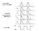
以下、図2の波形を用いて、E級増幅部511の動作を説明する。図2は、E級増幅部511に関連する信号の波形を示す。 Hereinafter, the operation of the class
周期信号発生部61からの信号によって、スイッチ部31はON/OFFを切り替える(図2(b))。いまスイッチ部31の状態がONからOFFに切り替わったとする。図1に示すA点の電圧波形は、図2(a)のように上昇する。これは、スイッチ部31が切り替わっても、電流量が変化しないようにL1が作用するためである。スイッチ部31がOFFになってもL1から電流が流れてくるため、C1に電荷が溜まることでA点の電圧が上昇する。しばらくすると、A点の電位上昇は収まり、つぎは電位が降下する。これは、C1に溜まった電荷が、L2、C2へと流れていくためである。 The
ここで、E級増幅部511が最適な効率で動作するためには、スイッチ部31をOFFからONに切り替えるときに、下記の2つの条件を満たす必要がある。すなわち、条件1は、A点の電圧が略0Vであること(スイッチ部31にバイポーラトランジスタを用いた場合にはコレクタ−エミッタ電圧が生じるため0Vとはならないように、全ての回路において0Vが条件ではなく、実現する回路において極力低電圧の状態であること)である。また条件2は、電圧波形の傾きが略0であることである。 Here, in order for the class
図2上のA点の波形は、上記の2つの条件を満たしている。これは、E級増幅部511から送信共振回路部91をみた負荷に応じて、E級増幅部511のL1、C1、L2、C2の値を適切に設定することで可能となる。このとき、E級増幅部511は図2(c)の波形のような、ほぼ正弦波の波形を有する電圧を出力する。なお、厳密には正弦波でなくてもよい。 The waveform at point A on FIG. 2 satisfies the above two conditions. This can be achieved by appropriately setting the values of L1, C1, L2, and C2 of the class
スイッチ部31のB点は、検出部41を介してグランドまたはアース(本明細書では「GND」とも記述する)に接続されている。 The B point of the
検出部41は、スイッチ部31からGNDへ流れる電流もしくはB点の電圧を検出し、その検出結果を信号抽出部221へと出力する。たとえば検出部41は、電流を電圧に変換する抵抗素子を配置することにより実現される。抵抗素子を利用してスイッチ部31からGNDへ流れる電流を検出できる。検出部41は、後述するように受電機器2側でのインピーダンス可変部42でのインピーダンス値の変化に応じて変化する、スイッチ部31のB点を流れる電流の波形を検出する。 The
信号抽出部221は、検出部41で検出された波形の変化(電流波形311)から、データ信号の有無を判定し、データ信号が存在する場合にはそのデータ信号321を抽出する。このデータ信号が表すデータは、受電機器2から送電機器1に送信されたデータである。データの種類は任意である。データは、たとえば受電機器2から送電機器1に送信されたコマンドであってもよい。 The
なお、信号抽出部221がデータ信号の有無を判定することは必須ではない。信号抽出部221は、受け取った電流波形311から直接に信号を抽出してもよい。この結果得られた所定の振幅を有する信号が、データ信号321として取り扱われる。 It is not essential for the
E級増幅部511の出力は、送信共振回路部91から、電磁結合された受電機器2の受信共振回路部92へと伝送される。受信共振回路部92で受信された交流信号は、整流回路部52で整流され、インピーダンス可変部42を介して電力再生部82へと入力される。電力再生部82は、入力された信号を受電機器2の回路へ供給される電源電力として出力する。 The output of the class
以上、送電機器1から受電機器2へと電力が無線伝送される動作を説明した。 The operation in which power is wirelessly transmitted from the
次に、受電機器2から送電機器1へとデータを伝送する動作を説明する。 Next, an operation for transmitting data from the power receiving device 2 to the
受電機器2が送電機器1へデータ伝送するとき、整流回路部52と電力再生部82の間のインピーダンス可変部42は、インピーダンス値を変化させる。これにより、送電機器1において、E級増幅部511から送信共振回路部91を見たインピーダンス値が変化する。 When the power receiving device 2 transmits data to the
このとき、E級増幅部511のA点の波形が、前述の最適なE級増幅動作から外れることになり、図3(a)〜(e)に示すように波形が変化する。図3(a)は、インピーダンスが最適のときのE級増幅部511のA点の波形を示し、図3(b)〜(e)はインピーダンスが最適ではないときのA点の波形の変化を示す。また図3(f)は、スイッチ部31のオン/オフ動作タイミングを示す。図3(b)〜(e)の波形は、前述したE級増幅部511が最適な効率で動作するための2つの条件が満たされていないことを示す。 At this time, the waveform at point A of the class
A点の波形変化は、下記に示すように主に4つの波形形状に分けられる。
(1)スイッチがONからOFFに変化した後、電圧が上昇して、単調減少している状態でスイッチがOFFからONに切り替わり、しばらく放電して略0Vになる(図3(b))。
(2)スイッチがONからOFFに変化した後、電圧が上昇して、減少して、再び上昇している状態でスイッチがOFFからONに切り替わり、しばらく放電して略0Vになる(図3(c))。
(3)スイッチがONからOFFに変化した後、電圧が上昇して、減少して略0Vまで落ちて略0Vが続いたあと、再び上昇している状態でスイッチがOFFからONに切り替わり、しばらく放電して略0Vになる(図3(d))。
(4)スイッチがONからOFFに変化した後、電圧が上昇して、減少して略0Vまで落ちて、略0Vの状態のままスイッチがOFFからONに切り替わり、略0Vの状態が継続する(図3(e))。The waveform change at point A is mainly divided into four waveform shapes as shown below.
(1) After the switch changes from ON to OFF, the voltage rises and the switch switches from OFF to ON in a monotonically decreasing state, and discharges for a while to reach approximately 0 V (FIG. 3B).
(2) After the switch changes from ON to OFF, the voltage increases, decreases, and rises again while the switch is switched from OFF to ON, and discharges for a while to become approximately 0 V (FIG. 3 ( c)).
(3) After the switch changes from ON to OFF, the voltage increases, decreases, decreases to approximately 0V, continues to approximately 0V, and then switches again from OFF to ON while increasing again. As a result of the discharge, the voltage becomes approximately 0 V (FIG. 3D).
(4) After the switch changes from ON to OFF, the voltage increases, decreases and drops to approximately 0V, and the switch is switched from OFF to ON while maintaining approximately 0V, and the approximately 0V state continues ( FIG. 3 (e)).
本願発明者らは、受電機器2のインピーダンス可変部42のインピーダンス値を意図的に変化させてインピーダンスをあえて最適でない状態に遷移させ、それによって送電機器1において生じるA点の電流波形の変化を検出することで、受電機器2から送電機器1に送信されたデータ信号を抽出することが可能であることを見出した。 The inventors of the present application intentionally change the impedance value of the
より具体的に説明する。図4(a)は、インピーダンスが最適のときのA点における波形と、送電機器1の検出部41の電流検出波形とを示す。インピーダンスが最適のときは、電流検出波形に変化はない。 This will be described more specifically. FIG. 4A shows a waveform at point A when the impedance is optimal, and a current detection waveform of the
この状態から、図3(b)〜(d)までの波形変化が生じるように、受電機器2のインピーダンス可変部42がインピーダンス値を変化させる。そのとき、送電機器1の検出部41を流れる電流を検出すると、その電流には、たとえば図4(b)に示すような立ち上がり波形が含まれている。この電流は、図4(c)のようにスイッチ部31がOFFからONに切り替わった直後から放電が終わるまでの間において、E級増幅部511のスイッチ部31から放電される電流である。信号抽出部221は、その変化に基づいて、たとえばスイッチ部31がオフからオンに変化したときに立ち上がり波形が存在する場合には「1」、存在しない場合には「0」としてデータ信号を生成する。これにより、受電機器2から送電機器1へ送られるデータを検出することが可能となる。 From this state, the
なお、識別タイミングには送電機器1自身のクロックを用いることが可能である。送電機器1自身のクロックは通常、インピーダンス値の変化に起因するピークの立ち上がり開始から立ち下がりまでの時区間よりも充分短い。したがって、わずかの時区間で現れるピークを検出することは充分可能である。 Note that the clock of the
なお、上述の説明では、1つの立ち上がり波形に「1」を割り当てた。しかしながらこの処理は一例である。他の例として、スイッチ部31がオフからオンに切り替わるタイミングの電流検出波形を、切り替え複数回分監視し、立ち上がり波形が検出された回数、および、検出されなかった回数の比率に応じて「1」または「0」と判定してもよい。図1には、信号抽出部221が、電流波形の立ち上がりが4回含まれている電流検出波形311に基づいて、「1」に相当する受信データ信号321を生成している様子を示している。 In the above description, “1” is assigned to one rising waveform. However, this process is an example. As another example, the current detection waveform at the timing when the
また、スイッチ部31から放電される電流波形の変化は、スイッチ部31がOFFからONに切り替わった瞬間から放電が完了するまで生じる。よって、スイッチ部31を切り替える周期信号発生部61の出力信号をタイミング信号として用いれば、信号抽出部221でデータ判定するためのタイミング信号を別途設けなくとも、データ判定が可能となる。そのため、タイミング信号を生成するためのクロックデータリカバリー回路などを設ける必要がないので、回路の簡素化を図り、コスト増加を抑制できる。 The change in the waveform of the current discharged from the
以上より、送電機器1から受電機器2へ無線電力伝送する無線電力伝送システム100では、送電機器1にE級増幅部511を使用して受電機器2へ電力を伝送することが可能である。さらに、受電機器2のインピーダンス値を伝送したデータに応じて変化させ、E級増幅部511のスイッチ部31から放電される際の電流波形または電圧波形を検出することで、受電機器2から送電機器1へデータを伝送することが可能となる。 As described above, in the wireless
このデータの利用方法として、たとえば受電機器が受電を許可された機器か否かの判定または認証に利用することができる。正規の受電機器がたとえば定期的に「1」のデータを送電機器に伝送することにより、送電機器は、その受電機器が正規の受電機器であると判定できる。すると、送電機器は自らの送信共振回路と受電機器の受信共振回路とを共振周波数で電磁結合して、非接触で共振することにより、電力を伝送することができる。これにより、非正規の受電機器による盗電を防ぐことができる。伝送されるデータを、送電機器と受電機器とのペアリングのための情報として利用してもよい。 As a method of using this data, for example, it can be used to determine or authenticate whether or not the power receiving device is a device permitted to receive power. For example, when the regular power receiving device periodically transmits “1” data to the power transmitting device, the power transmitting device can determine that the power receiving device is a legitimate power receiving device. Then, the power transmission device can transmit electric power by electromagnetically coupling the transmission resonance circuit of the power transmission device and the reception resonance circuit of the power reception device at the resonance frequency and resonating without contact. Thereby, theft by the unauthorized power receiving device can be prevented. The transmitted data may be used as information for pairing between the power transmitting device and the power receiving device.
なお、本実施形態において、スイッチ部31は電界効果トランジスタやバイポーラトランジスタのような半導体を用いたスイッチング素子であったり、スイッチングの周波数が低ければ機械的なスイッチング素子であってもよく、2点間を接続/切断することのできるスイッチング素子であってもよい。 In the present embodiment, the
(実施形態2)
図5は、本実施形態における無線電力伝送システム110のブロック構成である。図5において、実施形態1の無線電力伝送システムと同じ構成要素については同じ符号を用い、説明を省略する。(Embodiment 2)
FIG. 5 is a block configuration of the wireless power transmission system 110 in the present embodiment. In FIG. 5, the same components as those in the wireless power transmission system according to the first embodiment are denoted by the same reference numerals, and the description thereof is omitted.
実施形態1では、受電機器2から送電機器1への片方向のデータ伝送を説明した。本実施形態では、送電機器1から受電機器2への無線での電力伝送だけでなく、E級増幅回路を用いて、送電機器1と受電機器2とで双方向のデータ伝送を行う無線電力伝送システム110を説明する。 In the first embodiment, one-way data transmission from the power receiving device 2 to the
以下、図5および図6を参照しながら、無線電力伝送システム110の構成および動作を説明する。図6(a)〜(e)は、無線電力伝送システム110内で生成または検出される信号波形を示す。 Hereinafter, the configuration and operation of the wireless power transmission system 110 will be described with reference to FIGS. 5 and 6. 6A to 6E show signal waveforms generated or detected in the wireless power transmission system 110. FIG.
図5において、第1の送信データ信号421(図6(a))を電圧制御部251へ入力する。第1の送信データ信号421(図6(a))は、送電機器1が受電機器2へ送りたいデータ信号と位置づけられる。 In FIG. 5, the first transmission data signal 421 (FIG. 6A) is input to the
電圧制御部251は、入力された所与の第1の送信データ信号421に応じて、電源191の出力電圧を図6(a)のように制御する。言い換えると、電圧制御部251は、電源191の出力電圧を、第1の送信データ信号421(図6(a))の波形変化と同じ波形変化を有するよう制御する。 The
このとき、電源191の出力電圧が変化すると、E級増幅部511の出力波形の振幅が、電源191の出力電圧に応じて変化する(図6(b))。これにより、E級増幅部511の出力に、振幅変調をかけることができる。電源191の出力電圧が変化すると、実施形態1で述べた、E級増幅部511のA点の波形は振幅方向に変化する。しかし、A点の波形は振幅が変化するだけであり、電源191の出力電圧が変化する前のA点の波形が例えば図4(b)に示す波形であれば、変化した後も図4(b)に示す波形となる。スイッチ部31がOFFからONに変わるタイミングで、図4(b)の電流検出波形を検出することは可能である。よって、実施形態1で説明した、受電機器2から送電機器1へのデータ伝送を、本実施形態においても同様に行うことは可能である。 At this time, when the output voltage of the
E級増幅部511の出力信号に図6(b)のような振幅変調がかかると、受電機器2の整流回路部52の出力にも、振幅変調された波形が得られる(図6(c))。整流回路部52の出力は、インピーダンス可変部42を介してデータ復調部292と電力再生部82へ入力される。電力再生部82は、受電機器2の回路へ供給される電力を出力する(図8(e))。一方、データ復調部292は、整流回路部52の出力信号に包絡線検波などの波形処理を行い、第1の受信データ信号422を出力する。これにより、送電機器1から送信されたデータを復調(または再生)することができる(図6(d))。 When amplitude modulation as shown in FIG. 6B is applied to the output signal of the class
以上説明した通り、本実施形態に係る無線電力伝送システム110では、送電機器1にE級増幅部511を使用して受電機器2へ無線で電力を伝送するとともに、送電機器1から受電機器2へデータを伝送することが可能である。送電機器1から受電機器2へのデータは、E級増幅部511の電源191の出力電圧を制御して、送電機器1から受電機器2へと伝送するデータ信号でE級増幅部511の出力を振幅変調することにより伝送される。一方、受電機器2から送電機器1へのデータは、実施形態1と同様に、受電機器2のインピーダンス値を伝送したデータに応じて変化させ、それに対応する電流波形変化を送電機器1において検出することによって伝送される。これにより、送電機器1と受電機器2の間でデータの双方向伝送が可能となる。 As described above, in the wireless power transmission system 110 according to this embodiment, the
なお、本実施形態では、電圧制御部251が電源191の出力電圧を制御してE級増幅部511の出力を振幅変調していたが、電圧制御部251が電源191の出力電圧をパルス幅変調することで、E級増幅部511の出力をパルス幅変調する構成であってもよい。E級増幅部511の電源191を制御してデータ変調をかける方式であればよい。 In this embodiment, the
なお、本実施形態では、図6で整流回路部52を全波整流の出力として図示しているが、半波整流であってもよく、データ復調と電源再生が可能となる整流方法であればよい。 In this embodiment, the
(実施形態3)
図7は、本実施形態における無線電力伝送システム120のブロック構成である。図7において、実施形態1および2の無線電力伝送システムと同じ構成要素については同じ符号を用い、説明を省略する。(Embodiment 3)
FIG. 7 is a block configuration of the wireless
実施形態2では、送電機器1から受電機器2へ伝送したいデータを、E級増幅部511の電源191を制御することでデータ変調する構成としていた。本実施形態では、E級増幅部511の入力波形である周期信号をパルス幅変調することでデータを変調する。 In the second embodiment, the data to be transmitted from the
以下、図7および図8を参照しながら、無線電力伝送システム110の構成および動作を説明する。図8(a)〜(e)は、無線電力伝送システム120内で生成または検出される信号波形を示す。 Hereinafter, the configuration and operation of the wireless power transmission system 110 will be described with reference to FIGS. 7 and 8. 8A to 8E show signal waveforms generated or detected in the wireless
PWM信号生成部291は、第1の送信データ信号421(図8(a))を、パルス幅変調し、図8(b)に示す信号を出力する。変調部111は、この信号と、周期信号発生部61の出力信号とを掛け合わせて、E級増幅部511のスイッチ部31へ入力する。 The PWM
E級増幅部511の出力は、スイッチ部31への入力が周期信号である期間は周期信号となり、スイッチ部31の入力が無い期間は無信号となる(図8(c))。E級増幅部511の出力は、送信共振回路部91から受信共振回路部92へ伝送されて、整流回路部52で整流される(図8(d))。 The output of the class
整流回路部52の出力は、インピーダンス可変部42を介して包絡線検波部452と電力再生部82へ入力される。電力再生部82は、受電機器2の回路へ供給される電力を出力する(図8(g))。一方、包絡線検波部452は、整流回路部52の出力信号を包絡線検波する(図8(e))。包絡線検波部452の出力信号は、送電機器1のPWM信号生成部291が出力したパルス幅変調信号と同じになる。PWM信号復調部332は、得られたパルス幅変調信号にPWM信号生成部291の処理と逆の処理(パルス幅復調)を行って、第1の受信データ信号422を出力する(図8(f))。 The output of the
受電機器2から送電機器1へデータ伝送する方法は、実施形態1とほぼ同様である。ただし、E級増幅部511をパルス幅変調された周期信号で変調している。そのため、周期信号がある期間は、図4(b)に示すような電流検出波形を検出することで受電機器2から送電機器1へのデータを検出することが可能となる。この場合、パルス幅変調されている関係上、周期信号がない期間があるため、スイッチ部31を流れる電流の変化を検出することができない。その期間についてはスイッチ部31を流れる電流は略0だからである。 A method for transmitting data from the power receiving device 2 to the
そのため、パルス幅変調された信号を伝送する本実施形態では、パルス幅変調された中の周期信号がある期間で、受電機器2から送電機器1へデータ伝送することになる。一例として、パルス幅変調する際に、1つのタイムスロット内で必ず周期信号がある(即ちパルス幅が0とはならない)ようにパルス幅変調する。そして、1つのタイムスロットで最低でも1ビットのデータを受電機器2から送電機器1へ伝送できるようにすることで、送電機器1から受電機器2へのデータレートと同じデータレートを維持できる。 Therefore, in the present embodiment in which a pulse width modulated signal is transmitted, data is transmitted from the power receiving device 2 to the
実施形態1では、周期信号発生部61の出力信号をタイミング信号として用いる構成を述べたが、上述のとおり周期信号がない期間はデータ判定をしても検出できない。そのため、変調部111の出力信号をタイミング信号として使用することで、周期信号のある期間は周期信号があるためその信号をタイミング信号としてデータを判定する。周期信号の無い期間は信号がないのでデータを判定しない。データを検出することができない期間のデータ判定を無効とすることができるため、データ判定の精度を高めることが可能となる。 In the first embodiment, the configuration in which the output signal of the
以上説明した通り、本実施形態に係る無線電力伝送システム120によっても、送電機器1にE級増幅部511を使用して受電機器2へ無線で電力を伝送するとともに、送電機器1から受電機器2へデータを伝送することが可能である。送電機器1から受電機器2へのデータは、E級増幅部511の入力信号である周期信号をパルス幅変調して、送電機器1から受電機器2へと伝送するデータ信号でE級増幅部511の出力をパルス幅変調することにより伝送される。一方、受電機器2から送電機器1へのデータは、実施形態1、2と同様に、受電機器2のインピーダンス値を伝送したデータに応じて変化させ、それに対応する電流波形変化を送電機器1において検出することによって伝送される。これにより、送電機器1と受電機器2の間でデータの双方向伝送が可能となる。 As described above, also by the wireless
なお、本実施形態では、図8で整流回路部52を全波整流の出力として図示しているが、半波整流であってもよく、データ復調と電源再生が可能となる整流方法であればよい。 In this embodiment, the
実施形態2および3においては、双方向のデータ伝送が可能である。たとえば、送信機器が応答を要求したタイミングで所定期間内に受電機器から応答があれば、送信機器はその受電機器を認証し、その後も受電させてもよい。応答がなければ、または、予め定められた応答ではなければ、送信機器はその受電機器を認証せず、電力の送信を停止してもよい。または、相互に伝送されるデータを、送電機器と受電機器とのペアリングのための情報として利用してもよい。 In the second and third embodiments, bidirectional data transmission is possible. For example, if there is a response from the power receiving device within a predetermined period at the timing when the transmission device requests a response, the transmitting device may authenticate the power receiving device and continue to receive power thereafter. If there is no response or if the response is not a predetermined response, the transmitting device may stop authenticating the power receiving device and stop transmitting power. Alternatively, data transmitted between each other may be used as information for pairing between the power transmitting device and the power receiving device.
上述の実施形態1〜3では、信号抽出部221は、検出部41で検出された波形の変化(電流波形311)からデータ信号の有無を判定し、データ信号が存在する場合にはそのデータ信号321を抽出すると説明した。しかしながら、信号抽出部221がデータ信号の有無を判定する動作は必須ではない。信号抽出部221は、検出部41が検出した信号波形から常に何らかの信号を抽出して出力してもよい。たとえば信号抽出部221は、検出部41の出力信号を継続的に受け取りながら、実施形態1においてデータ信号が存在する場合に行っていた処理をその出力信号に施す。その結果、検出部41から出力される信号波形にデータ信号が含まれている場合には、信号抽出部221は受信データ信号321を抽出する。一方、検出部41から出力される信号波形にデータ信号が含まれていない場合には、信号抽出部221は、波形に立ち上がりおよび立ち下がりが含まれない一定の信号を抽出する。信号抽出部221から出力される信号に受電機器2から送信されたデータが含まれているか否かの判断は、たとえば後段の処理回路(図示せず)が行えばよい。 In the above-described first to third embodiments, the
上述の実施形態、たとえば図1に示す実施形態1の例では、検出部41は、スイッチ部31からGNDへ流れる電流もしくはB点の電圧を検出する、と説明した。しかしながら、上述の検出方法によって電流もしくは電圧を検出するためには電流を流す必要がある。そのため、電力の損失が発生していた。 In the above-described embodiment, for example, the example of
そのような電力損失を低減するために、検出部41を設ける位置を変更すればよい。たとえば図9は、実施形態1の変形例にかかる無線電力伝送システム130のブロック構成を示している。無線電力伝送システム130が、実施形態1の無線電力伝送システム100と相違する点は、検出部241がA点の電圧を検出することである。この相違点に起因して、図9にはB点は示されていない。 In order to reduce such power loss, the position where the
以下、上述の相違点に関連する構成を説明する。その他の構成およびシステムの動作の詳細は実施形態1と同じであるから、その説明は省略する。 Hereinafter, a configuration related to the above-described difference will be described. Since other details of the configuration and the operation of the system are the same as those of the first embodiment, description thereof is omitted.
検出部241は、A点の電圧を検出する。このとき、A点から検出部241に電流が実質的に流れないようにするため、検出部241のインピーダンスを十分高く設定する必要がある。なお、A点では図3に示す電圧波形が検出されることになる。この電圧は比較的大きいため、検出部241および信号抽出部221には、想定される電圧に耐え得る程度の性能が必要である。すなわち、比較的耐圧を高く設定しなければならない。 The
上記構成によれば、受電機器2から送電機器1へとデータを伝送する動作に関連する電力損失を低減することができる。 According to the said structure, the power loss relevant to the operation | movement which transmits data from the power receiving apparatus 2 to the
なお、上述の図9の構成は一例である。実施形態2および3の各無線電力伝送システムの検出部に関しても全く同様に適用できる。すなわち、図5に記載の実施形態2にかかる無線電力伝送システム110、および、図7に記載の実施形態3にかかる無線電力伝送システム120において、図9に示す位置に、上述した特性を有する検出器241およびそれに接続される信号抽出部221を配置すればよい。 Note that the configuration of FIG. 9 described above is an example. The same applies to the detection units of the wireless power transmission systems of the second and third embodiments. That is, in the wireless power transmission system 110 according to the second embodiment described in FIG. 5 and the wireless
本発明にかかる無線電力伝送システムは、無線で電力を伝送する送電機器および受電機器の間で、データの一方向または双方向の伝送が可能である。このデータを利用して、たとえば無線で伝送された電力の受電を許可するかどうかの認証に利用することができる。本発明は、送電機器および受電機器を有する無線電力伝送システムとして実現される数多くの電気製品に対して有用である。 The wireless power transmission system according to the present invention is capable of unidirectional or bidirectional transmission of data between a power transmitting device and a power receiving device that transmit power wirelessly. Using this data, for example, it can be used to authenticate whether or not to allow the reception of power transmitted wirelessly. The present invention is useful for many electric products realized as a wireless power transmission system having a power transmitting device and a power receiving device.
1 送電機器
2 受電機器
21 整合回路部
31 スイッチ部
32 ICチップ
41 検出部
42 インピーダンス可変部
51 増幅部
52 整流回路部
61 周期信号発生部
62 制御部
82 電力再生部
9 変調部
91 送信共振回路部
92 受信共振回路部
101 復調部
111 変調部
131 無線送信部
141 無線受信部
171 サーキュレータ
191 電源
221 信号抽出部
251 電圧制御部
291 PWM信号生成部
292 データ復調部
332 PWM信号復調部
452 包絡線検波部
911 読取/書込装置
992 非接触ICカードDESCRIPTION OF
Claims (10)
Translated fromJapanese前記送電機器は、
周期信号を発生する周期信号発生部と、
前記周期信号発生部からの前記周期信号に応じてスイッチング動作するスイッチ部と、
直流電源と前記スイッチ部の一端を接続する第1のインダクタと、
前記スイッチ部の一端とグランドを接続する第1のキャパシタと、
前記スイッチ部の一端に接続された第2のインダクタと第2のキャパシタで構成されたLC共振回路部と、
前記LC共振回路部に接続され、前記周期信号の周期と略同じ共振周波数を有する送信共振回路部と、
前記スイッチ部の一端の電圧、または、前記スイッチ部の他端の電流もしくは電圧を検出する検出部と、
前記検出部の出力から信号を抽出する信号抽出部と、
前記送電機器から前記受電機器へ送信する第1の送信信号に応じて、前記直流電源の出力電圧を制御する電圧制御部と
を備え、かつ、前記周期信号で前記スイッチ部をスイッチング動作することで、前記直流電源から供給される電力を、前記周期信号と略同じ周波数を有する交流信号に変換するE級増幅動作を行い、
前記受電機器は、
前記送信共振回路部と電磁結合し、前記送信共振回路部と共振する受信共振回路部と、
前記受信共振回路部で受信した信号を整流する整流回路部と、
前記整流回路部と電力再生部を接続するインピーダンス可変部と、
前記インピーダンス可変部の出力から前記受電機器の電力を生成する電力再生部と、
前記インピーダンス可変部の出力から前記第1の送信信号を復調する復調部と、
前記受電機器から前記送電機器に伝送する第2の送信信号に応じて前記インピーダン
ス可変部のインピーダンスを切り替える制御部と
を備え、
前記電圧制御部は、前記第1の送信信号に応じて、前記直流電源の出力電圧をパルス幅変調することで、前記送信共振回路部から出力される信号が、前記送信共振回路部と前記受信共振回路部の共振周波数と略同じ周波数を持った交流信号を搬送波として、前記第1の送信信号でパルス幅変調した波形となる、無線電力伝送システム。A wireless power transmission device that wirelessly transmits power from a power transmission device to a power reception device,
The power transmission equipment is
A periodic signal generator for generating a periodic signal;
A switch unit that performs a switching operation according to the periodic signal from the periodic signal generation unit;
A first inductor connecting a DC power source and one end of the switch unit;
A first capacitor connecting one end of the switch unit and the ground;
An LC resonance circuit unit composed of a second inductor and a second capacitor connected to one end of the switch unit;
A transmission resonance circuit unit connected to the LC resonance circuit unit and having a resonance frequency substantially the same as the period of the periodic signal;
A detection unit that detects a voltage at one end of the switch unit, or a current or voltage at the other end of the switch unit;
A signal extraction unit for extracting a signal from the output of the detection unit;
A voltage control unit that controls an output voltage of the DC power supply according to a first transmission signal transmitted from the power transmission device to the power reception device, and switching the switch unit with the periodic signal. , Performing a class E amplification operation for converting the power supplied from the DC power source into an AC signal having substantially the same frequency as the periodic signal;
The power receiving device is:
A reception resonance circuit unit that is electromagnetically coupled to the transmission resonance circuit unit and resonates with the transmission resonance circuit unit;
A rectifier circuit unit for rectifying a signal received by the reception resonance circuit unit;
An impedance variable unit that connects the rectifier circuit unit and the power regeneration unit;
A power regeneration unit that generates power of the power receiving device from an output of the impedance variable unit;
A demodulator for demodulating the first transmission signal from the output of the impedance variable unit;
A control unit that switches the impedance of the impedance variable unit according to a second transmission signal transmitted from the power receiving device to the power transmission device,
The voltage control unit performs pulse width modulation on the output voltage of the DC power supply in accordance with the first transmission signal, so that a signal output from the transmission resonance circuit unit and the reception resonance circuit unit are received. A wireless power transmission system inwhich an AC signal having substantially the same frequency as a resonance frequency of a resonance circuit unit is used as a carrier wave, and a waveform is pulse-width modulated with the first transmission signal .
前記送電機器は、
周期信号を発生する周期信号発生部と、
前記送電機器から前記受電機器へ送信する第1の送信信号に応じて、パルス幅変調信号を生成するパルス幅変調信号生成部と、
前記周期信号を前記パルス幅変調信号で変調する変調部と、
前記変調部の出力に応じてスイッチング動作するスイッチ部と、
直流電源と前記スイッチ部の一端を接続する第1のインダクタと、
前記スイッチ部の一端とグランドを接続する第1のキャパシタと、
前記スイッチ部の一端に接続された第2のインダクタと第2のキャパシタで構成されたLC共振回路部と、
前記LC共振回路部に接続され、前記周期信号の周期と略同じ共振周波数を有する送信共振回路部と、
前記スイッチ部の一端の電圧、または、前記スイッチ部の他端の電流もしくは電圧を検出する検出部と、
前記検出部の出力から信号を抽出する信号抽出部と、
を備え、
前記受電機器は、
前記送信共振回路部と電磁結合し、前記送信共振回路部と共振する受信共振回路部と、
前記受信共振回路部で受信した信号を整流する整流回路部と、
前記整流回路部と電力再生部を接続するインピーダンス可変部と、
前記インピーダンス可変部の出力から前記受電機器の電力を生成する電力再生部と、
前記インピーダンス可変部の出力の包絡線を検波する包絡線検波部と、
前記包絡線検波部の出力から前記第1の送信信号を復調するパルス幅変調信号復調部と、
前記受電機器から前記送電機器に伝送する第2の送信信号に応じて前記インピーダンス可変部のインピーダンスを切り替える制御部と、
を備えた無線電力伝送システム。A wireless power transmission system that wirelessly transmits power from a power transmitting device to a power receiving device,
The power transmission equipment is
A periodic signal generator for generating a periodic signal;
In response to a first transmission signal transmitted from the power transmission device to the power receiving device, a pulse width modulation signal generation unit that generates a pulse width modulation signal;
A modulator for modulating the periodic signal with the pulse width modulation signal;
A switch unit that performs a switching operation according to the output of the modulation unit;
A first inductor connecting a DC power source and one end of the switch unit;
A first capacitor connecting one end of the switch unit and the ground;
An LC resonance circuit unit composed of a second inductor and a second capacitor connected to one end of the switch unit;
A transmission resonance circuit unit connected to the LC resonance circuit unit and having a resonance frequency substantially the same as the period of the periodic signal;
A detection unit that detects a voltage at one end of the switch unit, or a current or voltage at the other end of the switch unit;
A signal extraction unit for extracting a signal from the output of the detection unit;
With
The power receiving device is:
A reception resonance circuit unit that is electromagnetically coupled to the transmission resonance circuit unit and resonates with the transmission resonance circuit unit;
A rectifier circuit unit for rectifying a signal received by the reception resonance circuit unit;
An impedance variable unit that connects the rectifier circuit unit and the power regeneration unit;
A power regeneration unit that generates power of the power receiving device from an output of the impedance variable unit;
An envelope detector for detecting the envelope of the output of the impedance variable unit;
A pulse width modulation signal demodulator that demodulates the first transmission signal from the output of the envelope detector;
A control unit that switches the impedance of the impedance variable unit according to a second transmission signal transmitted from the power receiving device to the power transmission device;
Wireless power transmission system equipped with.
前記検出部が、前記スイッチ部の他端の電流もしくは電圧を検出する場合において、前記検出部は、前記スイッチ部からグランドに流れる電流によって生じる電圧を前記信号抽出部に入力し、
前記信号抽出部は、入力された電圧から前記信号を抽出する、請求項3から7のいずれかに記載の無線電力伝送システム。The detection unit is composed of a resistance element,
When the detection unit detects a current or voltage at the other end of the switch unit, the detection unit inputs a voltage generated by a current flowing from the switch unit to the ground to the signal extraction unit,
The wireless power transmission system accordingto claim3 , wherein the signal extraction unit extracts the signal from an input voltage.
前記送電機器は、
交流エネルギを生成するE級増幅部と、
前記交流エネルギを空間へ送出する送信共振回路部と、
前記E級増幅部の所定位置の電圧または電流の波形を検出する検出部であって、前記E級増幅部から前記送信共振回路部を見たときのインピーダンスに応じた波形を検出する検出部と、
前記波形に応じた信号を抽出する信号抽出部と、
周期信号を発生する周期信号発生部と、
送信対象となる送信をパルス幅変調するPWM信号生成部と、
前記周期信号とパルス幅変調された前記送信とを掛け合わせる変調部と
を備えており、
前記受電機器は、
前記送信共振回路部によって送出された前記交流エネルギの少なくとも一部を受け取る受信共振回路部と、
前記受信共振回路部によって受け取られた前記交流エネルギの少なくとも一部を整流して出力する整流回路部と、
前記整流回路部の出力に基づいて電力を出力する電力再生部と、
前記整流回路部と前記電力再生部との間に接続され、インピーダンスを切り替えるインピーダンス可変部と、
前記整流回路部の出力に包絡線検波の波形処理を行う包絡線検波部と、
前記波形処理が行われた前記整流回路部の出力にパルス幅復調を行い前記送信を出力するPWM信号復調部とを備え、
前記インピーダンス可変部が前記インピーダンスを切り替えることにより、前記検出部は前記インピーダンスが整合しているときの波形と整合していないときの波形とを検出し、前記信号抽出部は、前記検出部が検出した波形に応じた信号を抽出して出力する、無線電力伝送システム。A wireless power transmission system that wirelessly transmits power from a power transmitting device to a power receiving device,
The power transmission equipment is
A class E amplifier for generating AC energy;
A transmission resonance circuit section for sending the AC energy to space;
A detection unit for detecting a waveform of a voltage or current at a predetermined position of the class E amplification unit, the detection unit detecting a waveform according to an impedance when the transmission resonance circuit unit is viewed from the class E amplification unit; ,
A signal extraction unit for extracting a signal corresponding to the waveform;
A periodic signal generator for generating a periodic signal;
A PWM signal generator for pulse width modulating the transmission to be transmitted;
A modulation unit that multiplies the periodic signal and the pulse-width-modulated transmission, and
The power receiving device is:
A receiving resonant circuit unit that receives at least a portion of the AC energy transmitted by the transmitting resonant circuit unit;
A rectifier circuit unit that rectifies and outputs at least part of the AC energy received by the reception resonant circuit unit;
A power regeneration unit that outputs power based on the output of the rectifier circuit unit;
An impedance variable unit that is connected between the rectifier circuit unit and the power regeneration unit and switches impedance,
An envelope detector for performing waveform processing of envelope detection on the output of the rectifier circuit; and
A PWM signal demodulator that performs pulse width demodulation on the output of the rectifier circuit unit that has undergone the waveform processing and outputs the transmission ;
When the impedance variable unit switches the impedance, the detection unit detects a waveform when the impedance is matched and a waveform when the impedance is not matched, and the signal extraction unit is detected by the detection unit. A wireless power transmission system that extracts and outputs a signal corresponding to the waveform.
Priority Applications (2)
| Application Number | Priority Date | Filing Date | Title |
|---|---|---|---|
| JP2011263408AJP5670869B2 (en) | 2010-12-22 | 2011-12-01 | Wireless power transmission system |
| US13/329,433US8872385B2 (en) | 2010-12-22 | 2011-12-19 | Wireless power transmission system |
Applications Claiming Priority (3)
| Application Number | Priority Date | Filing Date | Title |
|---|---|---|---|
| JP2010285799 | 2010-12-22 | ||
| JP2010285799 | 2010-12-22 | ||
| JP2011263408AJP5670869B2 (en) | 2010-12-22 | 2011-12-01 | Wireless power transmission system |
Publications (2)
| Publication Number | Publication Date |
|---|---|
| JP2012146289A JP2012146289A (en) | 2012-08-02 |
| JP5670869B2true JP5670869B2 (en) | 2015-02-18 |
Family
ID=46315739
Family Applications (1)
| Application Number | Title | Priority Date | Filing Date |
|---|---|---|---|
| JP2011263408AActiveJP5670869B2 (en) | 2010-12-22 | 2011-12-01 | Wireless power transmission system |
Country Status (2)
| Country | Link |
|---|---|
| US (1) | US8872385B2 (en) |
| JP (1) | JP5670869B2 (en) |
Families Citing this family (58)
| Publication number | Priority date | Publication date | Assignee | Title |
|---|---|---|---|---|
| JP2013021887A (en)* | 2011-07-14 | 2013-01-31 | Equos Research Co Ltd | Electric power transmission system |
| JP5826547B2 (en)* | 2011-07-20 | 2015-12-02 | 株式会社豊田自動織機 | Power supply side equipment and resonance type non-contact power supply system |
| CA2788895C (en)* | 2011-09-07 | 2020-08-18 | Solace Power Inc. | Wireless electric field power transmission system and method |
| US9071284B2 (en) | 2011-10-21 | 2015-06-30 | Qualcomm Incorporated | Load impedance detection for static or dynamic adjustment of passive loads |
| IN2014CN02821A (en)* | 2011-10-21 | 2015-07-03 | Qualcomm Inc | |
| JP6074745B2 (en)* | 2012-01-25 | 2017-02-08 | パナソニックIpマネジメント株式会社 | Wireless power transmission system and power transmission device |
| TWI587597B (en)* | 2012-02-17 | 2017-06-11 | Lg伊諾特股份有限公司 | Wireless power transmitter, wireless power receiver, and power transmission method of wireless power transmitting system |
| CN104521106B (en) | 2012-07-10 | 2017-06-06 | 三星电子株式会社 | Wireless power transmitter, wireless power receiver and its control method |
| US9472958B2 (en)* | 2012-07-18 | 2016-10-18 | WIPQTUS Inc. | Wireless power system |
| RU2510558C1 (en)* | 2012-07-19 | 2014-03-27 | Александр Викторович Атаманов | Wireless charging system for low-power consumers of electrical energy |
| GB201215152D0 (en) | 2012-08-24 | 2012-10-10 | Imp Innovations Ltd | Maximising DC to load efficiency for inductive power transfer |
| KR102060337B1 (en)* | 2013-01-22 | 2019-12-31 | 삼성전자주식회사 | Reception node and transmission node using mutual resonance, power and data reception/transmission system using mutual resonance, method thereof |
| JP6334958B2 (en)* | 2013-04-04 | 2018-05-30 | キヤノン株式会社 | Power transmission apparatus, control method thereof, and program |
| KR102042674B1 (en)* | 2013-05-23 | 2019-11-11 | 삼성전자주식회사 | Apparatus and method for wireless power transmission |
| GB201321267D0 (en) | 2013-12-02 | 2014-01-15 | Imp Innovations Ltd | Inductive power transfer system |
| JP6276532B2 (en)* | 2013-07-29 | 2018-02-07 | キヤノン株式会社 | Power receiving device, power transmitting device, control method thereof, and program |
| CN103633749B (en)* | 2013-11-13 | 2016-03-02 | 华南理工大学 | A kind of resonance type wireless delivery of electrical energy radiating circuit |
| US10164472B2 (en) | 2013-12-03 | 2018-12-25 | Massachusetts Institute Of Technology | Method and apparatus for wirelessly charging portable electronic devices |
| KR101943082B1 (en)* | 2014-01-23 | 2019-04-18 | 한국전자통신연구원 | Wireless power transmission device, wireless power receiving device and wireless power transmission system |
| CN106030966B (en)* | 2014-02-19 | 2019-08-09 | 三星电子株式会社 | Method for detecting load in wireless charging |
| US9472366B2 (en)* | 2014-03-03 | 2016-10-18 | Divergent, Inc. | Generation and use of electric fields from capacitive effects of a solenoid |
| AR099614A1 (en)* | 2014-03-03 | 2016-08-03 | Divergent Inc | GENERATION AND USE OF MAGNETIC VECTOR POTENTIAL |
| US9373966B2 (en) | 2014-03-03 | 2016-06-21 | Divergent, Inc. | Wireless power and communication systems using magnetic vector potential |
| US9379555B2 (en)* | 2014-04-30 | 2016-06-28 | Active-Semi, Inc. | Adaptive power source for wireless power transmitter |
| EP3189581A4 (en) | 2014-09-05 | 2018-03-28 | Solace Power Inc. | Wireless electric field power transfer system, method, transmitter and receiver therefor |
| KR101730223B1 (en)* | 2014-10-27 | 2017-04-25 | 삼성전기주식회사 | Apparatus and method for receiving wireless power, and wireless power supply system using the same |
| US10498160B2 (en) | 2015-08-03 | 2019-12-03 | Massachusetts Institute Of Technology | Efficiency maximization for device-to-device wireless charging |
| US10199881B2 (en) | 2015-10-23 | 2019-02-05 | Mediatek Inc. | Robust foreign objects detection |
| JP6515015B2 (en)* | 2015-11-11 | 2019-05-15 | 株式会社ダイヘン | Contactless power transmission system |
| US11213687B2 (en)* | 2016-02-03 | 2022-01-04 | The Charles Stark Draper Laboratory, Inc. | Neural implant for microstimulation |
| WO2017171435A1 (en)* | 2016-03-31 | 2017-10-05 | 삼성전자 주식회사 | Wireless power transmission apparatus and method for controlling same |
| KR102560807B1 (en)* | 2016-05-30 | 2023-07-28 | 주식회사 위츠 | Resonance apparatus and apparatus for transmitting power wirelessly using the same |
| WO2018064791A1 (en)* | 2016-10-03 | 2018-04-12 | Intel Corporation | Reactance shift detection and over dissipation protection in a wireless power transmitter |
| US11606344B2 (en)* | 2017-05-10 | 2023-03-14 | Osr Enterprises Ag | Security enforcement in a system with a multiplicity of end units |
| US10423116B2 (en) | 2017-11-30 | 2019-09-24 | Canon Kabushiki Kaisha | Power supply apparatus and image forming apparatus having adjusted load power |
| US11701976B2 (en) | 2017-12-15 | 2023-07-18 | WiBotic Inc. | Device authentication for wireless charging |
| US11707996B2 (en) | 2017-12-15 | 2023-07-25 | WiBotic Inc. | Wireless charging with multiple charging locations |
| US10651687B2 (en) | 2018-02-08 | 2020-05-12 | Massachusetts Institute Of Technology | Detuning for a resonant wireless power transfer system including cryptography |
| US11018526B2 (en) | 2018-02-08 | 2021-05-25 | Massachusetts Institute Of Technology | Detuning for a resonant wireless power transfer system including cooperative power sharing |
| US11671032B2 (en)* | 2018-04-20 | 2023-06-06 | Nissan Motor Co., Ltd. | Control method for controlling resonance power converter, and resonance power converter |
| CN110417536B (en) | 2018-04-27 | 2021-12-31 | 华为技术有限公司 | Phase detection method and phase detection circuit |
| CN110945745B (en) | 2018-07-19 | 2023-09-01 | 联发科技(新加坡)私人有限公司 | Foreign object detection in a wireless power transfer system |
| EP3818620A4 (en) | 2018-07-19 | 2022-03-23 | MediaTek Singapore Pte. Ltd. | DETECTION OF FOREIGN OBJECTS IN WIRELESS POWER TRANSMISSION SYSTEMS |
| KR102700029B1 (en)* | 2018-07-30 | 2024-08-29 | 삼성전자주식회사 | Electronic device including a plurality of wireless charge coils and operating method thereof |
| CN111095723B (en) | 2018-09-29 | 2023-05-09 | 华为技术有限公司 | Wireless charging method and electronic device |
| EP3675311A1 (en)* | 2018-12-28 | 2020-07-01 | Vito NV | Energy storage string with energy management device |
| DE102019206836A1 (en)* | 2019-05-10 | 2020-11-12 | Fraunhofer-Gesellschaft zur Förderung der angewandten Forschung e.V. | Efficient communication for configuring sensor nodes |
| TWI741958B (en) | 2021-03-05 | 2021-10-01 | 國立陽明交通大學 | Minimum power input control method |
| KR102492319B1 (en)* | 2021-07-08 | 2023-01-26 | 고려대학교 산학협력단 | Back data transmission circuit and method that is robust to load changes |
| CN113541329B (en)* | 2021-07-12 | 2023-05-26 | 清华大学深圳国际研究生院 | Wireless energy transmission system with global power control function |
| CN113690012B (en)* | 2021-08-24 | 2023-05-12 | 合肥市武汉大学创新技术研究院 | Controllable inductor and flexible high-efficiency multi-resonance wireless power transmission system |
| JP7712618B2 (en)* | 2021-10-05 | 2025-07-24 | アクト電子株式会社 | Insulation/short circuit switching device for insulated wheels, track maintenance vehicle, and insulation/short circuit switching method for insulated wheels |
| CN113809842B (en)* | 2021-11-16 | 2022-04-12 | 深圳赫兹创新技术有限公司 | Automatic matching method and device for wireless charging receiving terminal, transmitting terminal and system |
| CN114043882A (en)* | 2021-11-16 | 2022-02-15 | 桔充充(杭州)新能源有限公司 | A wireless charging system suitable for a variety of two-wheeled electric vehicle batteries |
| KR102797801B1 (en)* | 2021-12-30 | 2025-04-17 | 한양대학교 산학협력단 | Apparatus for wireless power and two-way data transmission using single coil |
| US20240088711A1 (en)* | 2022-09-09 | 2024-03-14 | Stmicroelectronics Asia Pacific Pte Ltd. | Power regulation in wireless power transmitter |
| CN116111738A (en)* | 2023-02-09 | 2023-05-12 | 兆赫兹(深圳)科技有限公司 | Transmitter of wireless power transmission system |
| KR20240146483A (en) | 2023-03-29 | 2024-10-08 | 삼성전자주식회사 | Reception circuit and smart card including the same |
Family Cites Families (9)
| Publication number | Priority date | Publication date | Assignee | Title |
|---|---|---|---|---|
| AT395224B (en) | 1990-08-23 | 1992-10-27 | Mikron Ges Fuer Integrierte Mi | CONTACTLESS, INDUCTIVE DATA TRANSFER SYSTEM |
| JPH10256957A (en)* | 1997-03-13 | 1998-09-25 | Nagano Japan Radio Co | Power transmission device and power transmission system |
| EP1615158B1 (en)* | 2002-12-24 | 2014-08-27 | Panasonic Corp | Contactless smart card reader |
| JP2004206245A (en) | 2002-12-24 | 2004-07-22 | Matsushita Electric Ind Co Ltd | Non-contact IC card reading / writing device |
| JP2005018404A (en)* | 2003-06-26 | 2005-01-20 | Matsushita Electric Ind Co Ltd | Inductive read / write communication terminal and communication system using the same |
| JP4891100B2 (en)* | 2007-01-17 | 2012-03-07 | セイコーエプソン株式会社 | Power reception control device, power reception device, and electronic device |
| JP4561796B2 (en) | 2007-08-31 | 2010-10-13 | ソニー株式会社 | Power receiving device and power transmission system |
| US20090284369A1 (en) | 2008-05-13 | 2009-11-19 | Qualcomm Incorporated | Transmit power control for a wireless charging system |
| US8532724B2 (en) | 2008-09-17 | 2013-09-10 | Qualcomm Incorporated | Transmitters for wireless power transmission |
- 2011
- 2011-12-01JPJP2011263408Apatent/JP5670869B2/enactiveActive
- 2011-12-19USUS13/329,433patent/US8872385B2/enactiveActive
Also Published As
| Publication number | Publication date |
|---|---|
| US8872385B2 (en) | 2014-10-28 |
| US20120161538A1 (en) | 2012-06-28 |
| JP2012146289A (en) | 2012-08-02 |
Similar Documents
| Publication | Publication Date | Title |
|---|---|---|
| JP5670869B2 (en) | Wireless power transmission system | |
| US10367368B2 (en) | Wireless power transfer method and wireless power transmitter | |
| US9791888B2 (en) | Power reception device and power transmission system | |
| CN105281444B (en) | Wireless power transmission method, apparatus and system | |
| US7919886B2 (en) | Power receiving device and power transfer system | |
| EP2128804B1 (en) | Transponder and interrogator | |
| US9590446B2 (en) | Apparatus and method for wireless charging | |
| CN103545938B (en) | Wireless power transmission method, device and system | |
| US8403233B2 (en) | Semiconductor integrated circuit device and IC card mounting same | |
| JP4637204B2 (en) | Communication apparatus and antenna characteristic control method | |
| US8493185B2 (en) | Radio frequency identification reader antenna having a dynamically adjustable Q-factor | |
| KR102034323B1 (en) | Power supply device, power supply method and recording medium | |
| CN102823111B (en) | Power transmission device and waveform monitoring circuit used therein | |
| KR20170043764A (en) | Multi-coil wireless charging method and apparatus and system therefor | |
| US20120223592A1 (en) | Method for driving power supply system | |
| JP2013009373A (en) | Communication device using wireless power, system, and method | |
| UA57016C2 (en) | System for data communication between a terminal and a mobile object with wireless communication line and distant power supply of the mobile object equipment | |
| JP5395018B2 (en) | Resonant type wireless power transmission device | |
| US9581977B2 (en) | Appliance management apparatus and appliance management method | |
| JP3891421B2 (en) | Electronic circuit, modulation method, and information processing apparatus and method | |
| US20130211607A1 (en) | Power supplying apparatus and power supplying method | |
| JP2008028791A (en) | Class E amplifier, reader / writer and document management system using the same | |
| KR20180047517A (en) | Wireless power transmitter and method for controlling sampling in wireless power transmitter | |
| JP3892563B2 (en) | Information storage medium | |
| JP6234700B2 (en) | COMMUNICATION SYSTEM, TRANSMISSION DEVICE, AND TRANSMITTING / RECEIVING METHOD |
Legal Events
| Date | Code | Title | Description |
|---|---|---|---|
| A621 | Written request for application examination | Free format text:JAPANESE INTERMEDIATE CODE: A621 Effective date:20140306 | |
| A977 | Report on retrieval | Free format text:JAPANESE INTERMEDIATE CODE: A971007 Effective date:20140911 | |
| A131 | Notification of reasons for refusal | Free format text:JAPANESE INTERMEDIATE CODE: A131 Effective date:20140930 | |
| A711 | Notification of change in applicant | Free format text:JAPANESE INTERMEDIATE CODE: A711 Effective date:20141008 | |
| A521 | Request for written amendment filed | Free format text:JAPANESE INTERMEDIATE CODE: A523 Effective date:20141128 | |
| TRDD | Decision of grant or rejection written | ||
| A01 | Written decision to grant a patent or to grant a registration (utility model) | Free format text:JAPANESE INTERMEDIATE CODE: A01 Effective date:20141216 | |
| A61 | First payment of annual fees (during grant procedure) | Free format text:JAPANESE INTERMEDIATE CODE: A61 Effective date:20141218 | |
| R151 | Written notification of patent or utility model registration | Ref document number:5670869 Country of ref document:JP Free format text:JAPANESE INTERMEDIATE CODE: R151 |