JP5663305B2 - Method and apparatus for atomic layer deposition using atmospheric pressure glow discharge plasma - Google Patents
Method and apparatus for atomic layer deposition using atmospheric pressure glow discharge plasmaDownload PDFInfo
- Publication number
- JP5663305B2 JP5663305B2JP2010523971AJP2010523971AJP5663305B2JP 5663305 B2JP5663305 B2JP 5663305B2JP 2010523971 AJP2010523971 AJP 2010523971AJP 2010523971 AJP2010523971 AJP 2010523971AJP 5663305 B2JP5663305 B2JP 5663305B2
- Authority
- JP
- Japan
- Prior art keywords
- substrate
- gas mixture
- gas
- precursor
- processing space
- Prior art date
- Legal status (The legal status is an assumption and is not a legal conclusion. Google has not performed a legal analysis and makes no representation as to the accuracy of the status listed.)
- Active
Links
- 238000000034methodMethods0.000titleclaimsdescription95
- 238000000231atomic layer depositionMethods0.000titleclaimsdescription50
- 239000000758substrateSubstances0.000claimsdescription183
- 239000007789gasSubstances0.000claimsdescription151
- 239000000203mixtureSubstances0.000claimsdescription134
- 239000002243precursorSubstances0.000claimsdescription133
- 238000012545processingMethods0.000claimsdescription131
- 239000011261inert gasSubstances0.000claimsdescription84
- 239000000463materialSubstances0.000claimsdescription68
- 239000000376reactantSubstances0.000claimsdescription55
- 239000010410layerSubstances0.000claimsdescription54
- 238000006243chemical reactionMethods0.000claimsdescription44
- 238000000151depositionMethods0.000claimsdescription25
- 239000002356single layerSubstances0.000claimsdescription18
- 239000007795chemical reaction productSubstances0.000claimsdescription14
- 230000005684electric fieldEffects0.000claimsdescription14
- 238000002347injectionMethods0.000claimsdescription8
- 239000007924injectionSubstances0.000claimsdescription8
- 230000003750conditioning effectEffects0.000claimsdescription4
- 238000012546transferMethods0.000claimsdescription2
- 239000003153chemical reaction reagentSubstances0.000claims1
- 210000002381plasmaAnatomy0.000description116
- 230000008569processEffects0.000description33
- IJGRMHOSHXDMSA-UHFFFAOYSA-NAtomic nitrogenChemical compoundN#NIJGRMHOSHXDMSA-UHFFFAOYSA-N0.000description26
- 229910052757nitrogenInorganic materials0.000description21
- QGZKDVFQNNGYKY-UHFFFAOYSA-NAmmoniaChemical compoundNQGZKDVFQNNGYKY-UHFFFAOYSA-N0.000description14
- QVGXLLKOCUKJST-UHFFFAOYSA-Natomic oxygenChemical compound[O]QVGXLLKOCUKJST-UHFFFAOYSA-N0.000description12
- 239000010408filmSubstances0.000description12
- 239000001301oxygenSubstances0.000description12
- 229910052760oxygenInorganic materials0.000description12
- 230000008021depositionEffects0.000description11
- 238000005229chemical vapour depositionMethods0.000description10
- 230000004888barrier functionEffects0.000description9
- JLTRXTDYQLMHGR-UHFFFAOYSA-NtrimethylaluminiumChemical compoundC[Al](C)CJLTRXTDYQLMHGR-UHFFFAOYSA-N0.000description9
- 238000010926purgeMethods0.000description8
- 229910021529ammoniaInorganic materials0.000description7
- 230000008859changeEffects0.000description7
- 229910018072Al 2 O 3Inorganic materials0.000description6
- XKRFYHLGVUSROY-UHFFFAOYSA-NArgonChemical compound[Ar]XKRFYHLGVUSROY-UHFFFAOYSA-N0.000description6
- 238000010586diagramMethods0.000description6
- 125000002887hydroxy groupChemical group[H]O*0.000description6
- 238000005240physical vapour depositionMethods0.000description6
- 230000000087stabilizing effectEffects0.000description6
- 239000002344surface layerSubstances0.000description6
- 239000010409thin filmSubstances0.000description6
- XLYOFNOQVPJJNP-UHFFFAOYSA-NwaterSubstancesOXLYOFNOQVPJJNP-UHFFFAOYSA-N0.000description6
- 239000012159carrier gasSubstances0.000description5
- 238000011010flushing procedureMethods0.000description5
- 229910052756noble gasInorganic materials0.000description5
- 238000009832plasma treatmentMethods0.000description5
- 238000006557surface reactionMethods0.000description5
- 230000032683agingEffects0.000description4
- 150000001412aminesChemical class0.000description4
- 239000003795chemical substances by applicationSubstances0.000description4
- 150000001875compoundsChemical class0.000description4
- 238000005137deposition processMethods0.000description4
- 229910001873dinitrogenInorganic materials0.000description4
- 239000011888foilSubstances0.000description4
- 238000004519manufacturing processMethods0.000description4
- 230000007246mechanismEffects0.000description4
- 229910052751metalInorganic materials0.000description4
- 239000002184metalSubstances0.000description4
- 150000002835noble gasesChemical class0.000description4
- 239000004033plasticSubstances0.000description4
- 229920003023plasticPolymers0.000description4
- CURLTUGMZLYLDI-UHFFFAOYSA-NCarbon dioxideChemical compoundO=C=OCURLTUGMZLYLDI-UHFFFAOYSA-N0.000description3
- CBENFWSGALASAD-UHFFFAOYSA-NOzoneChemical compound[O-][O+]=OCBENFWSGALASAD-UHFFFAOYSA-N0.000description3
- VYPSYNLAJGMNEJ-UHFFFAOYSA-NSilicium dioxideChemical compoundO=[Si]=OVYPSYNLAJGMNEJ-UHFFFAOYSA-N0.000description3
- 239000007983Tris bufferSubstances0.000description3
- 229910052782aluminiumInorganic materials0.000description3
- 229910052786argonInorganic materials0.000description3
- 239000000919ceramicSubstances0.000description3
- 239000011521glassSubstances0.000description3
- 229910052739hydrogenInorganic materials0.000description3
- 238000009616inductively coupled plasmaMethods0.000description3
- XEEYBQQBJWHFJM-UHFFFAOYSA-NironSubstances[Fe]XEEYBQQBJWHFJM-UHFFFAOYSA-N0.000description3
- 239000003446ligandSubstances0.000description3
- 229920000642polymerPolymers0.000description3
- 229920000307polymer substratePolymers0.000description3
- 150000003254radicalsChemical class0.000description3
- 229910052814silicon oxideInorganic materials0.000description3
- 239000000126substanceSubstances0.000description3
- 229910052715tantalumInorganic materials0.000description3
- GUVRBAGPIYLISA-UHFFFAOYSA-Ntantalum atomChemical compound[Ta]GUVRBAGPIYLISA-UHFFFAOYSA-N0.000description3
- 235000012431wafersNutrition0.000description3
- UFHFLCQGNIYNRP-UHFFFAOYSA-NHydrogenChemical compound[H][H]UFHFLCQGNIYNRP-UHFFFAOYSA-N0.000description2
- PXHVJJICTQNCMI-UHFFFAOYSA-NNickelChemical compound[Ni]PXHVJJICTQNCMI-UHFFFAOYSA-N0.000description2
- MWUXSHHQAYIFBG-UHFFFAOYSA-NNitric oxideChemical compoundO=[N]MWUXSHHQAYIFBG-UHFFFAOYSA-N0.000description2
- GQPLMRYTRLFLPF-UHFFFAOYSA-NNitrous OxideChemical compound[O-][N+]#NGQPLMRYTRLFLPF-UHFFFAOYSA-N0.000description2
- 229910008051Si-OHInorganic materials0.000description2
- 229910003902SiCl 4Inorganic materials0.000description2
- 229910006358Si—OHInorganic materials0.000description2
- XAGFODPZIPBFFR-UHFFFAOYSA-NaluminiumChemical compound[Al]XAGFODPZIPBFFR-UHFFFAOYSA-N0.000description2
- 125000004429atomChemical group0.000description2
- 230000008901benefitEffects0.000description2
- 230000015572biosynthetic processEffects0.000description2
- 210000004027cellAnatomy0.000description2
- 230000001143conditioned effectEffects0.000description2
- 239000004020conductorSubstances0.000description2
- 238000010924continuous productionMethods0.000description2
- 238000009792diffusion processMethods0.000description2
- 238000010494dissociation reactionMethods0.000description2
- 208000018459dissociative diseaseDiseases0.000description2
- 150000004820halidesChemical class0.000description2
- 239000001257hydrogenSubstances0.000description2
- 238000009434installationMethods0.000description2
- 229910052742ironInorganic materials0.000description2
- 150000002739metalsChemical class0.000description2
- QJGQUHMNIGDVPM-UHFFFAOYSA-Nnitrogen groupChemical group[N]QJGQUHMNIGDVPM-UHFFFAOYSA-N0.000description2
- 238000004806packaging method and processMethods0.000description2
- 229910052698phosphorusInorganic materials0.000description2
- BASFCYQUMIYNBI-UHFFFAOYSA-NplatinumChemical compound[Pt]BASFCYQUMIYNBI-UHFFFAOYSA-N0.000description2
- 239000002861polymer materialSubstances0.000description2
- 238000007781pre-processingMethods0.000description2
- 229920006395saturated elastomerPolymers0.000description2
- 239000004065semiconductorSubstances0.000description2
- 229910052710siliconInorganic materials0.000description2
- 229910052717sulfurInorganic materials0.000description2
- 229920001169thermoplasticPolymers0.000description2
- 239000010936titaniumSubstances0.000description2
- 229910052719titaniumInorganic materials0.000description2
- WFKWXMTUELFFGS-UHFFFAOYSA-NtungstenChemical compound[W]WFKWXMTUELFFGS-UHFFFAOYSA-N0.000description2
- 229910052721tungstenInorganic materials0.000description2
- 239000010937tungstenSubstances0.000description2
- 229910001868waterInorganic materials0.000description2
- 229910052727yttriumInorganic materials0.000description2
- VWQVUPCCIRVNHF-UHFFFAOYSA-Nyttrium atomChemical compound[Y]VWQVUPCCIRVNHF-UHFFFAOYSA-N0.000description2
- SDTMFDGELKWGFT-UHFFFAOYSA-N2-methylpropan-2-olateChemical compoundCC(C)(C)[O-]SDTMFDGELKWGFT-UHFFFAOYSA-N0.000description1
- MGWGWNFMUOTEHG-UHFFFAOYSA-N4-(3,5-dimethylphenyl)-1,3-thiazol-2-amineChemical compoundCC1=CC(C)=CC(C=2N=C(N)SC=2)=C1MGWGWNFMUOTEHG-UHFFFAOYSA-N0.000description1
- OXJUCLBTTSNHOF-UHFFFAOYSA-N5-ethylcyclopenta-1,3-diene;ruthenium(2+)Chemical compound[Ru+2].CC[C-]1C=CC=C1.CC[C-]1C=CC=C1OXJUCLBTTSNHOF-UHFFFAOYSA-N0.000description1
- ZOXJGFHDIHLPTG-UHFFFAOYSA-NBoronChemical compound[B]ZOXJGFHDIHLPTG-UHFFFAOYSA-N0.000description1
- NMGMAOIYXASREJ-UHFFFAOYSA-NC(C)C1(C=CC=C1)[Mn]C1(C=CC=C1)CCChemical compoundC(C)C1(C=CC=C1)[Mn]C1(C=CC=C1)CCNMGMAOIYXASREJ-UHFFFAOYSA-N0.000description1
- LIEOGMBLMOOSAY-UHFFFAOYSA-NCC1=C(C)C(C)([Mg]C2(C)C(C)=C(C)C(C)=C2C)C(C)=C1CChemical compoundCC1=C(C)C(C)([Mg]C2(C)C(C)=C(C)C(C)=C2C)C(C)=C1CLIEOGMBLMOOSAY-UHFFFAOYSA-N0.000description1
- YGBYJRVGNBVTCQ-UHFFFAOYSA-NC[Pt](C)C.[CH]1C=CC=C1Chemical compoundC[Pt](C)C.[CH]1C=CC=C1YGBYJRVGNBVTCQ-UHFFFAOYSA-N0.000description1
- VYZAMTAEIAYCRO-UHFFFAOYSA-NChromiumChemical compound[Cr]VYZAMTAEIAYCRO-UHFFFAOYSA-N0.000description1
- RYGMFSIKBFXOCR-UHFFFAOYSA-NCopperChemical compound[Cu]RYGMFSIKBFXOCR-UHFFFAOYSA-N0.000description1
- VMQMZMRVKUZKQL-UHFFFAOYSA-NCu+Chemical compound[Cu+]VMQMZMRVKUZKQL-UHFFFAOYSA-N0.000description1
- CWYNVVGOOAEACU-UHFFFAOYSA-NFe2+Chemical compound[Fe+2]CWYNVVGOOAEACU-UHFFFAOYSA-N0.000description1
- GYHNNYVSQQEPJS-UHFFFAOYSA-NGalliumChemical compound[Ga]GYHNNYVSQQEPJS-UHFFFAOYSA-N0.000description1
- FYYHWMGAXLPEAU-UHFFFAOYSA-NMagnesiumChemical compound[Mg]FYYHWMGAXLPEAU-UHFFFAOYSA-N0.000description1
- ZOKXTWBITQBERF-UHFFFAOYSA-NMolybdenumChemical compound[Mo]ZOKXTWBITQBERF-UHFFFAOYSA-N0.000description1
- PTUVJLQMNKPIOJ-UHFFFAOYSA-NN-[bis(diethylamino)alumanyl]-N-ethylethanamine trimethylalumaneChemical compoundC[Al](C)C.CCN(CC)[Al](N(CC)CC)N(CC)CCPTUVJLQMNKPIOJ-UHFFFAOYSA-N0.000description1
- VEQPNABPJHWNSG-UHFFFAOYSA-NNickel(2+)Chemical compound[Ni+2]VEQPNABPJHWNSG-UHFFFAOYSA-N0.000description1
- OAICVXFJPJFONN-UHFFFAOYSA-NPhosphorusChemical compound[P]OAICVXFJPJFONN-UHFFFAOYSA-N0.000description1
- 239000004698PolyethyleneSubstances0.000description1
- KJTLSVCANCCWHF-UHFFFAOYSA-NRutheniumChemical compound[Ru]KJTLSVCANCCWHF-UHFFFAOYSA-N0.000description1
- 229910020175SiOHInorganic materials0.000description1
- BLRPTPMANUNPDV-UHFFFAOYSA-NSilaneChemical compound[SiH4]BLRPTPMANUNPDV-UHFFFAOYSA-N0.000description1
- XUIMIQQOPSSXEZ-UHFFFAOYSA-NSiliconChemical compound[Si]XUIMIQQOPSSXEZ-UHFFFAOYSA-N0.000description1
- BQCADISMDOOEFD-UHFFFAOYSA-NSilverChemical compound[Ag]BQCADISMDOOEFD-UHFFFAOYSA-N0.000description1
- NINIDFKCEFEMDL-UHFFFAOYSA-NSulfurChemical compound[S]NINIDFKCEFEMDL-UHFFFAOYSA-N0.000description1
- ATJFFYVFTNAWJD-UHFFFAOYSA-NTinChemical compound[Sn]ATJFFYVFTNAWJD-UHFFFAOYSA-N0.000description1
- RTAQQCXQSZGOHL-UHFFFAOYSA-NTitaniumChemical compound[Ti]RTAQQCXQSZGOHL-UHFFFAOYSA-N0.000description1
- HCHKCACWOHOZIP-UHFFFAOYSA-NZincChemical compound[Zn]HCHKCACWOHOZIP-UHFFFAOYSA-N0.000description1
- QCWXUUIWCKQGHC-UHFFFAOYSA-NZirconiumChemical compound[Zr]QCWXUUIWCKQGHC-UHFFFAOYSA-N0.000description1
- USZGMDQWECZTIQ-UHFFFAOYSA-N[Mg](C1C=CC=C1)C1C=CC=C1Chemical compound[Mg](C1C=CC=C1)C1C=CC=C1USZGMDQWECZTIQ-UHFFFAOYSA-N0.000description1
- IHRNDXJDUYVDRB-UHFFFAOYSA-N[Ni].Cc1cccc1.Cc1cccc1Chemical compound[Ni].Cc1cccc1.Cc1cccc1IHRNDXJDUYVDRB-UHFFFAOYSA-N0.000description1
- 125000001931aliphatic groupChemical group0.000description1
- 125000003368amide groupChemical group0.000description1
- 229910052787antimonyInorganic materials0.000description1
- WATWJIUSRGPENY-UHFFFAOYSA-Nantimony atomChemical compound[Sb]WATWJIUSRGPENY-UHFFFAOYSA-N0.000description1
- 229910052785arsenicInorganic materials0.000description1
- RQNWIZPPADIBDY-UHFFFAOYSA-Narsenic atomChemical compound[As]RQNWIZPPADIBDY-UHFFFAOYSA-N0.000description1
- 125000003118aryl groupChemical group0.000description1
- 229910052788bariumInorganic materials0.000description1
- DSAJWYNOEDNPEQ-UHFFFAOYSA-Nbarium atomChemical compound[Ba]DSAJWYNOEDNPEQ-UHFFFAOYSA-N0.000description1
- 229910052790berylliumInorganic materials0.000description1
- ATBAMAFKBVZNFJ-UHFFFAOYSA-Nberyllium atomChemical compound[Be]ATBAMAFKBVZNFJ-UHFFFAOYSA-N0.000description1
- 230000005540biological transmissionEffects0.000description1
- 229910052797bismuthInorganic materials0.000description1
- JCXGWMGPZLAOME-UHFFFAOYSA-Nbismuth atomChemical compound[Bi]JCXGWMGPZLAOME-UHFFFAOYSA-N0.000description1
- 229910052796boronInorganic materials0.000description1
- RUUJZWYITYFKCY-UHFFFAOYSA-Nbutan-2-yl-(n-butan-2-yl-c-methylcarbonimidoyl)azanide;copper(1+)Chemical compound[Cu+].[Cu+].CCC(C)[N-]C(C)=NC(C)CC.CCC(C)[N-]C(C)=NC(C)CCRUUJZWYITYFKCY-UHFFFAOYSA-N0.000description1
- 239000006227byproductSubstances0.000description1
- 229910002092carbon dioxideInorganic materials0.000description1
- 239000001569carbon dioxideSubstances0.000description1
- FQNHWXHRAUXLFU-UHFFFAOYSA-Ncarbon monoxide;tungstenChemical group[W].[O+]#[C-].[O+]#[C-].[O+]#[C-].[O+]#[C-].[O+]#[C-].[O+]#[C-]FQNHWXHRAUXLFU-UHFFFAOYSA-N0.000description1
- 229910002090carbon oxideInorganic materials0.000description1
- 230000015556catabolic processEffects0.000description1
- 229910052729chemical elementInorganic materials0.000description1
- 229910052804chromiumInorganic materials0.000description1
- 239000011651chromiumSubstances0.000description1
- 238000000576coating methodMethods0.000description1
- 229910017052cobaltInorganic materials0.000description1
- 239000010941cobaltSubstances0.000description1
- GUTLYIVDDKVIGB-UHFFFAOYSA-Ncobalt atomChemical compound[Co]GUTLYIVDDKVIGB-UHFFFAOYSA-N0.000description1
- XLJKHNWPARRRJB-UHFFFAOYSA-Ncobalt(2+)Chemical compound[Co+2]XLJKHNWPARRRJB-UHFFFAOYSA-N0.000description1
- 229910052802copperInorganic materials0.000description1
- 239000010949copperSubstances0.000description1
- 230000007547defectEffects0.000description1
- 238000006731degradation reactionMethods0.000description1
- UZBQIPPOMKBLAS-UHFFFAOYSA-NdiethylazanideChemical compoundCC[N-]CCUZBQIPPOMKBLAS-UHFFFAOYSA-N0.000description1
- DXKNERXVNFFIOM-UHFFFAOYSA-Ndiethylazanide;di(propan-2-yl)azanide;titanium(4+)Chemical compoundCCN(CC)[Ti](N(CC)CC)(N(C(C)C)C(C)C)N(C(C)C)C(C)CDXKNERXVNFFIOM-UHFFFAOYSA-N0.000description1
- VBCSQFQVDXIOJL-UHFFFAOYSA-Ndiethylazanide;hafnium(4+)Chemical compound[Hf+4].CC[N-]CC.CC[N-]CC.CC[N-]CC.CC[N-]CCVBCSQFQVDXIOJL-UHFFFAOYSA-N0.000description1
- VJDVOZLYDLHLSM-UHFFFAOYSA-Ndiethylazanide;titanium(4+)Chemical compound[Ti+4].CC[N-]CC.CC[N-]CC.CC[N-]CC.CC[N-]CCVJDVOZLYDLHLSM-UHFFFAOYSA-N0.000description1
- GOVWJRDDHRBJRW-UHFFFAOYSA-Ndiethylazanide;zirconium(4+)Chemical compound[Zr+4].CC[N-]CC.CC[N-]CC.CC[N-]CC.CC[N-]CCGOVWJRDDHRBJRW-UHFFFAOYSA-N0.000description1
- HQWPLXHWEZZGKY-UHFFFAOYSA-NdiethylzincChemical compoundCC[Zn]CCHQWPLXHWEZZGKY-UHFFFAOYSA-N0.000description1
- VXGHASBVNMHGDI-UHFFFAOYSA-NdigermaneChemical compound[Ge][Ge]VXGHASBVNMHGDI-UHFFFAOYSA-N0.000description1
- JJQZDUKDJDQPMQ-UHFFFAOYSA-Ndimethoxy(dimethyl)silaneChemical compoundCO[Si](C)(C)OCJJQZDUKDJDQPMQ-UHFFFAOYSA-N0.000description1
- ZYLGGWPMIDHSEZ-UHFFFAOYSA-Ndimethylazanide;hafnium(4+)Chemical compound[Hf+4].C[N-]C.C[N-]C.C[N-]C.C[N-]CZYLGGWPMIDHSEZ-UHFFFAOYSA-N0.000description1
- DWCMDRNGBIZOQL-UHFFFAOYSA-Ndimethylazanide;zirconium(4+)Chemical compound[Zr+4].C[N-]C.C[N-]C.C[N-]C.C[N-]CDWCMDRNGBIZOQL-UHFFFAOYSA-N0.000description1
- PZPGRFITIJYNEJ-UHFFFAOYSA-NdisilaneChemical compound[SiH3][SiH3]PZPGRFITIJYNEJ-UHFFFAOYSA-N0.000description1
- 238000005538encapsulationMethods0.000description1
- 230000007613environmental effectEffects0.000description1
- GCPCLEKQVMKXJM-UHFFFAOYSA-Nethoxy(diethyl)alumaneChemical compoundCCO[Al](CC)CCGCPCLEKQVMKXJM-UHFFFAOYSA-N0.000description1
- NPEOKFBCHNGLJD-UHFFFAOYSA-Nethyl(methyl)azanide;hafnium(4+)Chemical compound[Hf+4].CC[N-]C.CC[N-]C.CC[N-]C.CC[N-]CNPEOKFBCHNGLJD-UHFFFAOYSA-N0.000description1
- LNKYFCABELSPAN-UHFFFAOYSA-Nethyl(methyl)azanide;titanium(4+)Chemical compound[Ti+4].CC[N-]C.CC[N-]C.CC[N-]C.CC[N-]CLNKYFCABELSPAN-UHFFFAOYSA-N0.000description1
- SRLSISLWUNZOOB-UHFFFAOYSA-Nethyl(methyl)azanide;zirconium(4+)Chemical compound[Zr+4].CC[N-]C.CC[N-]C.CC[N-]C.CC[N-]CSRLSISLWUNZOOB-UHFFFAOYSA-N0.000description1
- JFDAACUVRQBXJO-UHFFFAOYSA-Nethylcyclopentane;magnesiumChemical compound[Mg].CC[C]1[CH][CH][CH][CH]1.CC[C]1[CH][CH][CH][CH]1JFDAACUVRQBXJO-UHFFFAOYSA-N0.000description1
- 230000007717exclusionEffects0.000description1
- 229910052733galliumInorganic materials0.000description1
- 229910052732germaniumInorganic materials0.000description1
- GNPVGFCGXDBREM-UHFFFAOYSA-Ngermanium atomChemical compound[Ge]GNPVGFCGXDBREM-UHFFFAOYSA-N0.000description1
- 230000009477glass transitionEffects0.000description1
- PCHJSUWPFVWCPO-UHFFFAOYSA-NgoldChemical compound[Au]PCHJSUWPFVWCPO-UHFFFAOYSA-N0.000description1
- 229910052737goldInorganic materials0.000description1
- 239000010931goldSubstances0.000description1
- 229910052735hafniumInorganic materials0.000description1
- VBJZVLUMGGDVMO-UHFFFAOYSA-Nhafnium atomChemical compound[Hf]VBJZVLUMGGDVMO-UHFFFAOYSA-N0.000description1
- PDPJQWYGJJBYLF-UHFFFAOYSA-Jhafnium tetrachlorideChemical compoundCl[Hf](Cl)(Cl)ClPDPJQWYGJJBYLF-UHFFFAOYSA-J0.000description1
- 238000010438heat treatmentMethods0.000description1
- RLYZRADFTORPLZ-UHFFFAOYSA-Nhydroxy-tri(propan-2-yloxy)silaneChemical compoundCC(C)O[Si](O)(OC(C)C)OC(C)CRLYZRADFTORPLZ-UHFFFAOYSA-N0.000description1
- ORJFXWYTRPGGRK-UHFFFAOYSA-Nhydroxy-tris(2-methylbutan-2-yloxy)silaneChemical compoundCCC(C)(C)O[Si](O)(OC(C)(C)CC)OC(C)(C)CCORJFXWYTRPGGRK-UHFFFAOYSA-N0.000description1
- HLDBBQREZCVBMA-UHFFFAOYSA-Nhydroxy-tris[(2-methylpropan-2-yl)oxy]silaneChemical compoundCC(C)(C)O[Si](O)(OC(C)(C)C)OC(C)(C)CHLDBBQREZCVBMA-UHFFFAOYSA-N0.000description1
- 238000002513implantationMethods0.000description1
- 238000011835investigationMethods0.000description1
- 239000011133leadSubstances0.000description1
- 229910052749magnesiumInorganic materials0.000description1
- 239000011777magnesiumSubstances0.000description1
- WPBNNNQJVZRUHP-UHFFFAOYSA-Lmanganese(2+);methyl n-[[2-(methoxycarbonylcarbamothioylamino)phenyl]carbamothioyl]carbamate;n-[2-(sulfidocarbothioylamino)ethyl]carbamodithioateChemical compound[Mn+2].[S-]C(=S)NCCNC([S-])=S.COC(=O)NC(=S)NC1=CC=CC=C1NC(=S)NC(=O)OCWPBNNNQJVZRUHP-UHFFFAOYSA-L0.000description1
- QSHDDOUJBYECFT-UHFFFAOYSA-NmercuryChemical compound[Hg]QSHDDOUJBYECFT-UHFFFAOYSA-N0.000description1
- 229910052753mercuryInorganic materials0.000description1
- 125000002496methyl groupChemical group[H]C([H])([H])*0.000description1
- UIUXUFNYAYAMOE-UHFFFAOYSA-NmethylsilaneChemical compound[SiH3]CUIUXUFNYAYAMOE-UHFFFAOYSA-N0.000description1
- 229910052750molybdenumInorganic materials0.000description1
- 239000011733molybdenumSubstances0.000description1
- CUZHTAHNDRTVEF-UHFFFAOYSA-Nn-[bis(dimethylamino)alumanyl]-n-methylmethanamineChemical compound[Al+3].C[N-]C.C[N-]C.C[N-]CCUZHTAHNDRTVEF-UHFFFAOYSA-N0.000description1
- ZUSRFDBQZSPBDV-UHFFFAOYSA-Nn-[bis(dimethylamino)stibanyl]-n-methylmethanamineChemical compoundCN(C)[Sb](N(C)C)N(C)CZUSRFDBQZSPBDV-UHFFFAOYSA-N0.000description1
- 229910052759nickelInorganic materials0.000description1
- 229910052758niobiumInorganic materials0.000description1
- 239000010955niobiumSubstances0.000description1
- GUCVJGMIXFAOAE-UHFFFAOYSA-Nniobium atomChemical compound[Nb]GUCVJGMIXFAOAE-UHFFFAOYSA-N0.000description1
- ZTILUDNICMILKJ-UHFFFAOYSA-Nniobium(v) ethoxideChemical compoundCCO[Nb](OCC)(OCC)(OCC)OCCZTILUDNICMILKJ-UHFFFAOYSA-N0.000description1
- 238000006396nitration reactionMethods0.000description1
- JCXJVPUVTGWSNB-UHFFFAOYSA-Nnitrogen dioxideInorganic materialsO=[N]=OJCXJVPUVTGWSNB-UHFFFAOYSA-N0.000description1
- 229960001730nitrous oxideDrugs0.000description1
- 235000013842nitrous oxideNutrition0.000description1
- HMMGMWAXVFQUOA-UHFFFAOYSA-NoctamethylcyclotetrasiloxaneChemical compoundC[Si]1(C)O[Si](C)(C)O[Si](C)(C)O[Si](C)(C)O1HMMGMWAXVFQUOA-UHFFFAOYSA-N0.000description1
- 239000013110organic ligandSubstances0.000description1
- 150000002902organometallic compoundsChemical class0.000description1
- 229910052762osmiumInorganic materials0.000description1
- SYQBFIAQOQZEGI-UHFFFAOYSA-Nosmium atomChemical compound[Os]SYQBFIAQOQZEGI-UHFFFAOYSA-N0.000description1
- 125000004430oxygen atomChemical groupO*0.000description1
- 239000011574phosphorusSubstances0.000description1
- 238000000623plasma-assisted chemical vapour depositionMethods0.000description1
- 229910052697platinumInorganic materials0.000description1
- -1polyethylenePolymers0.000description1
- 229920000573polyethylenePolymers0.000description1
- 238000003672processing methodMethods0.000description1
- 239000000047productSubstances0.000description1
- 239000012713reactive precursorSubstances0.000description1
- 229910052707rutheniumInorganic materials0.000description1
- 238000004904shorteningMethods0.000description1
- 229910000077silaneInorganic materials0.000description1
- 239000010703siliconSubstances0.000description1
- 229910052709silverInorganic materials0.000description1
- 239000004332silverSubstances0.000description1
- 238000005507sprayingMethods0.000description1
- 230000035882stressEffects0.000description1
- 239000011593sulfurSubstances0.000description1
- 229920002994synthetic fiberPolymers0.000description1
- 238000012360testing methodMethods0.000description1
- MNWRORMXBIWXCI-UHFFFAOYSA-Ntetrakis(dimethylamido)titaniumChemical compoundCN(C)[Ti](N(C)C)(N(C)C)N(C)CMNWRORMXBIWXCI-UHFFFAOYSA-N0.000description1
- ZRLCXMPFXYVHGS-UHFFFAOYSA-NtetramethylgermaneChemical compoundC[Ge](C)(C)CZRLCXMPFXYVHGS-UHFFFAOYSA-N0.000description1
- RSNQKPMXXVDJFG-UHFFFAOYSA-NtetrasiloxaneChemical compound[SiH3]O[SiH2]O[SiH2]O[SiH3]RSNQKPMXXVDJFG-UHFFFAOYSA-N0.000description1
- 229920001187thermosetting polymerPolymers0.000description1
- 239000004634thermosetting polymerSubstances0.000description1
- 238000000427thin-film depositionMethods0.000description1
- 229910052718tinInorganic materials0.000description1
- 239000011135tinSubstances0.000description1
- 230000007723transport mechanismEffects0.000description1
- WOZZOSDBXABUFO-UHFFFAOYSA-Ntri(butan-2-yloxy)alumaneChemical compound[Al+3].CCC(C)[O-].CCC(C)[O-].CCC(C)[O-]WOZZOSDBXABUFO-UHFFFAOYSA-N0.000description1
- WXRGABKACDFXMG-UHFFFAOYSA-NtrimethylboraneChemical compoundCB(C)CWXRGABKACDFXMG-UHFFFAOYSA-N0.000description1
- XCZXGTMEAKBVPV-UHFFFAOYSA-NtrimethylgalliumChemical compoundC[Ga](C)CXCZXGTMEAKBVPV-UHFFFAOYSA-N0.000description1
- 125000000026trimethylsilyl groupChemical group[H]C([H])([H])[Si]([*])(C([H])([H])[H])C([H])([H])[H]0.000description1
- LENZDBCJOHFCAS-UHFFFAOYSA-NtrisChemical compoundOCC(N)(CO)COLENZDBCJOHFCAS-UHFFFAOYSA-N0.000description1
- 238000009827uniform distributionMethods0.000description1
- 229910052720vanadiumInorganic materials0.000description1
- GPPXJZIENCGNKB-UHFFFAOYSA-NvanadiumChemical compound[V]#[V]GPPXJZIENCGNKB-UHFFFAOYSA-N0.000description1
- 238000005406washingMethods0.000description1
- 238000004804windingMethods0.000description1
- 229910052725zincInorganic materials0.000description1
- 239000011701zincSubstances0.000description1
- 229910052726zirconiumInorganic materials0.000description1
Images


Classifications
- C—CHEMISTRY; METALLURGY
- C23—COATING METALLIC MATERIAL; COATING MATERIAL WITH METALLIC MATERIAL; CHEMICAL SURFACE TREATMENT; DIFFUSION TREATMENT OF METALLIC MATERIAL; COATING BY VACUUM EVAPORATION, BY SPUTTERING, BY ION IMPLANTATION OR BY CHEMICAL VAPOUR DEPOSITION, IN GENERAL; INHIBITING CORROSION OF METALLIC MATERIAL OR INCRUSTATION IN GENERAL
- C23C—COATING METALLIC MATERIAL; COATING MATERIAL WITH METALLIC MATERIAL; SURFACE TREATMENT OF METALLIC MATERIAL BY DIFFUSION INTO THE SURFACE, BY CHEMICAL CONVERSION OR SUBSTITUTION; COATING BY VACUUM EVAPORATION, BY SPUTTERING, BY ION IMPLANTATION OR BY CHEMICAL VAPOUR DEPOSITION, IN GENERAL
- C23C16/00—Chemical coating by decomposition of gaseous compounds, without leaving reaction products of surface material in the coating, i.e. chemical vapour deposition [CVD] processes
- C23C16/44—Chemical coating by decomposition of gaseous compounds, without leaving reaction products of surface material in the coating, i.e. chemical vapour deposition [CVD] processes characterised by the method of coating
- C23C16/448—Chemical coating by decomposition of gaseous compounds, without leaving reaction products of surface material in the coating, i.e. chemical vapour deposition [CVD] processes characterised by the method of coating characterised by the method used for generating reactive gas streams, e.g. by evaporation or sublimation of precursor materials
- C23C16/452—Chemical coating by decomposition of gaseous compounds, without leaving reaction products of surface material in the coating, i.e. chemical vapour deposition [CVD] processes characterised by the method of coating characterised by the method used for generating reactive gas streams, e.g. by evaporation or sublimation of precursor materials by activating reactive gas streams before their introduction into the reaction chamber, e.g. by ionisation or addition of reactive species
- C—CHEMISTRY; METALLURGY
- C23—COATING METALLIC MATERIAL; COATING MATERIAL WITH METALLIC MATERIAL; CHEMICAL SURFACE TREATMENT; DIFFUSION TREATMENT OF METALLIC MATERIAL; COATING BY VACUUM EVAPORATION, BY SPUTTERING, BY ION IMPLANTATION OR BY CHEMICAL VAPOUR DEPOSITION, IN GENERAL; INHIBITING CORROSION OF METALLIC MATERIAL OR INCRUSTATION IN GENERAL
- C23C—COATING METALLIC MATERIAL; COATING MATERIAL WITH METALLIC MATERIAL; SURFACE TREATMENT OF METALLIC MATERIAL BY DIFFUSION INTO THE SURFACE, BY CHEMICAL CONVERSION OR SUBSTITUTION; COATING BY VACUUM EVAPORATION, BY SPUTTERING, BY ION IMPLANTATION OR BY CHEMICAL VAPOUR DEPOSITION, IN GENERAL
- C23C16/00—Chemical coating by decomposition of gaseous compounds, without leaving reaction products of surface material in the coating, i.e. chemical vapour deposition [CVD] processes
- C23C16/02—Pretreatment of the material to be coated
- C23C16/0227—Pretreatment of the material to be coated by cleaning or etching
- C23C16/0245—Pretreatment of the material to be coated by cleaning or etching by etching with a plasma
- C—CHEMISTRY; METALLURGY
- C23—COATING METALLIC MATERIAL; COATING MATERIAL WITH METALLIC MATERIAL; CHEMICAL SURFACE TREATMENT; DIFFUSION TREATMENT OF METALLIC MATERIAL; COATING BY VACUUM EVAPORATION, BY SPUTTERING, BY ION IMPLANTATION OR BY CHEMICAL VAPOUR DEPOSITION, IN GENERAL; INHIBITING CORROSION OF METALLIC MATERIAL OR INCRUSTATION IN GENERAL
- C23C—COATING METALLIC MATERIAL; COATING MATERIAL WITH METALLIC MATERIAL; SURFACE TREATMENT OF METALLIC MATERIAL BY DIFFUSION INTO THE SURFACE, BY CHEMICAL CONVERSION OR SUBSTITUTION; COATING BY VACUUM EVAPORATION, BY SPUTTERING, BY ION IMPLANTATION OR BY CHEMICAL VAPOUR DEPOSITION, IN GENERAL
- C23C16/00—Chemical coating by decomposition of gaseous compounds, without leaving reaction products of surface material in the coating, i.e. chemical vapour deposition [CVD] processes
- C23C16/44—Chemical coating by decomposition of gaseous compounds, without leaving reaction products of surface material in the coating, i.e. chemical vapour deposition [CVD] processes characterised by the method of coating
- C23C16/455—Chemical coating by decomposition of gaseous compounds, without leaving reaction products of surface material in the coating, i.e. chemical vapour deposition [CVD] processes characterised by the method of coating characterised by the method used for introducing gases into reaction chamber or for modifying gas flows in reaction chamber
- C23C16/45523—Pulsed gas flow or change of composition over time
- C23C16/45525—Atomic layer deposition [ALD]
- C23C16/45527—Atomic layer deposition [ALD] characterized by the ALD cycle, e.g. different flows or temperatures during half-reactions, unusual pulsing sequence, use of precursor mixtures or auxiliary reactants or activations
- C23C16/45536—Use of plasma, radiation or electromagnetic fields
- C23C16/4554—Plasma being used non-continuously in between ALD reactions
Landscapes
- Chemical & Material Sciences (AREA)
- Engineering & Computer Science (AREA)
- Materials Engineering (AREA)
- General Chemical & Material Sciences (AREA)
- Chemical Kinetics & Catalysis (AREA)
- Mechanical Engineering (AREA)
- Metallurgy (AREA)
- Organic Chemistry (AREA)
- Plasma & Fusion (AREA)
- Physics & Mathematics (AREA)
- Electromagnetism (AREA)
- Chemical Vapour Deposition (AREA)
- Electroluminescent Light Sources (AREA)
Description
Translated fromJapanese本発明は、基板の表面に原子層を堆積する方法に関する。別の態様では、本発明は、大気圧プラズマシステムを含む、基板の表面に原子層を堆積する装置に関する。本発明のさらに別の態様では、この装置は、化学物質又は化学元素の堆積に使用される。 The present invention relates to a method for depositing an atomic layer on a surface of a substrate. In another aspect, the invention relates to an apparatus for depositing an atomic layer on a surface of a substrate, including an atmospheric pressure plasma system. In yet another aspect of the invention, the apparatus is used for chemical or chemical element deposition.
原子層堆積法(ALD)は、ある材料の層を基板の表面に形成するために当技術分野で用いられている。化学気相成長法(CVD)及び物理気相成長法(PVD)とは異なり、原子層堆積法(ALD)は飽和表面反応に基づく。ALDプロセスの固有面制御機構は、基板反応部位(sites)と前駆体分子の間で個々に順次行われる表面反応の飽和に基づく。この飽和機構では、膜成長速度が、CVD及びPVDにおけるように反応物濃度又は成長時間ではなく、反応サイクル数に直接比例することになる。 Atomic layer deposition (ALD) is used in the art to form a layer of a material on the surface of a substrate. Unlike chemical vapor deposition (CVD) and physical vapor deposition (PVD), atomic layer deposition (ALD) is based on a saturated surface reaction. The inherent surface control mechanism of the ALD process is based on the saturation of surface reactions that are performed individually and sequentially between the substrate reaction sites and the precursor molecules. With this saturation mechanism, the film growth rate will be directly proportional to the number of reaction cycles rather than the reactant concentration or growth time as in CVD and PVD.
Joo−Hyeon Leeの論文「前駆体としてSiH2Cl2及びO3を用いた原子層堆積による酸化シリコン薄膜の検討(Investigation of silicon oxide thin films by atomic layer deposition using SiH2Cl2 and O3 as the precursors)」では、前駆体としてSiH2Cl2及びオゾンを用いたALDにより酸化シリコン薄膜を堆積する方法を開示している。オゾンは、遠隔コロナプラズマ放電を用いて得られる。層は、300℃という高い処理温度で堆積される。Joo-Hyeon Lee study thesis, "the silicon oxide film bySiH 2 Cl2 andO 3 atomic layer deposition using a precursor (Investigation of silicon oxide thin films by atomic layer
米国特許出願公開第2005/0084610号は、基板の表面に原子層を堆積する化学気相成長プロセスを開示している。この堆積プロセスは、堆積プロセス中にラジカル発生器、例えば大気圧グロー放電プラズマなどのプラズマ発生器を使用することでより効果的になる。開示されたプロセスでは、前駆体分子は、表面と反応する前に分解される。 US Patent Application Publication No. 2005/0084610 discloses a chemical vapor deposition process that deposits an atomic layer on the surface of a substrate. This deposition process is made more effective by using a radical generator during the deposition process, for example a plasma generator such as an atmospheric pressure glow discharge plasma. In the disclosed process, precursor molecules are degraded before reacting with the surface.
米国特許第6,897,119B1号は、非常に薄い膜の堆積を実現するALDの装置及び方法を開示している。遠隔プラズマ発生器が使用されるが(図11の参照数字39)、その具体的な詳細については説明の中で言及されていない。反応チャンバ31は真空ポンプ36に接続されており、このことは、このプロセスが非常に低圧の環境であることを示す。 US Pat. No. 6,897,119 B1 discloses an ALD apparatus and method that achieves very thin film deposition. A remote plasma generator is used (reference numeral 39 in FIG. 11), but its specific details are not mentioned in the description. The
米国特許出願公開第2003/114018号は、半導体部品を製造する方法を開示している。ALDプロセスを使用し、単分子層の堆積の前にまず基板の表面をコンディショニングすることによって、誘電体層が形成される。第1ステップ(表面コンディショニング)は、フリーラジカル発生器の利用を含み、パルスO2プラズマ処理、パルスH2プラズマ処理、及びパルスNH3プラズマ処理などの例が言及されている。U.S. Patent Application Publication No. 2003/114018 discloses a method of manufacturing a semiconductor component. Using an ALD process, the dielectric layer is formed by first conditioning the surface of the substrate prior to monolayer deposition. The first step (surface conditioning) involves the use of a free radical generator, and examples such as pulse O2 plasma treatment, pulse H2 plasma treatment, and pulse NH3 plasma treatment are mentioned.
ALDは自己制御式の反応プロセスであり、即ち、堆積される前駆体分子の量が、基板表面の反応表面部位の数だけで決まり、飽和後の前駆体への露出とは無関係である。理論上、最大成長速度は、1サイクルあたりちょうど1単分子層であるが、ほとんどの場合、種々の理由により成長速度は、単分子層の0.2〜0.3に限定される。ALDサイクルは4つのステップからなる。これは一般に、単一の処理空間で実施される。これは、ステップ1として基板の表面に反応部位(sites)を形成することから開始する。次のステップとして、前駆体を反応部位と反応させ、過剰な材料及び反応生成物を処理空間外に除去すると、理想的には、前駆体の単分子層が反応表面部位を介して基板表面に付着して残る(ステップ2)。反応剤が処理空間の中に導入されると、付着した前駆体分子と反応して、反応部位を有する所望の材料の単分子層が再び形成され(ステップ3)、この後、反応しなかった材料及び副生成物が除外される。任意選択で、このサイクルは、追加の単分子層を堆積するために繰り返される(ステップ4)。各サイクルで基本的に1つの原子層を堆積することができ、これにより、膜厚及び膜特性の非常に正確な制御が可能になる。 ALD is a self-controlled reaction process, i.e., the amount of precursor molecules deposited depends solely on the number of reactive surface sites on the substrate surface and is independent of exposure to the precursor after saturation. Theoretically, the maximum growth rate is exactly one monolayer per cycle, but in most cases the growth rate is limited to 0.2-0.3 for monolayers for various reasons. The ALD cycle consists of four steps. This is generally performed in a single processing space. This starts with the formation of reaction sites on the surface of the substrate as step 1. The next step is to react the precursor with the reaction site and remove excess material and reaction products out of the processing space. Ideally, the precursor monolayer is transferred to the substrate surface via the reaction surface site. It remains attached (step 2). When the reactant is introduced into the processing space, it reacts with the attached precursor molecules to form again a monolayer of the desired material with reactive sites (step 3), after which it did not react. Materials and by-products are excluded. Optionally, this cycle is repeated to deposit additional monolayers (step 4). In each cycle, essentially one atomic layer can be deposited, which allows very precise control of film thickness and film properties.
従来技術では、このALDプロセス中の反応ステップを向上させるいくつかの方法、例えば熱ALD及びプラズマ支援ALDが開発されてきた。既知のALD法で使用されるプラズマは、低圧RFプラズマ又は誘導結合プラズマ(ICP)とすることができ、Al2O3、HfO2、Ta2O5、及び他の多くの材料を堆積するのに使用することができる。In the prior art, several methods have been developed to improve the reaction steps during this ALD process, such as thermal ALD and plasma assisted ALD. The plasma used in the known ALD method can be low pressure RF plasma or inductively coupled plasma (ICP), which deposits Al2 O3 , HfO2 , Ta2 O5 , and many other materials. Can be used for
国際特許公開WO01/15220は、集積回路内のバリア層の堆積の方法を記載しており、この方法ではALDが用いられる。ALDの各ステップでは、高温(最高500℃まで)の熱反応ステップと組み合わせて(約10トール(1330Pa)の)低圧が用いられる。別法として、反応環境を生成するのにプラズマを使用することが提案されている。開示されているすべての実施形態で、非常に低圧の環境が記載されており、そのため、使用される装置内には特別な対策が必要である。 International patent publication WO 01/15220 describes a method of depositing a barrier layer in an integrated circuit, in which ALD is used. Each ALD step uses a low pressure (about 10 Torr (1330 Pa)) in combination with a high temperature (up to 500 ° C.) thermal reaction step. Alternatively, it has been proposed to use a plasma to create a reaction environment. In all the disclosed embodiments, a very low pressure environment is described, so special measures are required in the equipment used.
米国特許出願公開第2004/0219784号は、熱反応ステップ又はプラズマ支援反応ステップを使用して原子層及び薄膜を形成する方法を開示しており、この方法では、ラジカルが基板から離れて形成されてから基板に移送される。やはり、これらのプロセスは、相対的に高温(100〜350℃)及び低圧(ほぼ真空、一般に0.3〜30トール(40〜4000Pa))で実施される。 US Patent Application Publication No. 2004/0219784 discloses a method of forming atomic layers and thin films using a thermal reaction step or a plasma assisted reaction step, wherein radicals are formed away from a substrate. To the substrate. Again, these processes are performed at relatively high temperatures (100-350 ° C.) and low pressure (almost vacuum, generally 0.3-30 torr (40-4000 Pa)).
米国特許出願公開第2003/0049375号はプラズマ支援CVDプロセスを使用して基板上に薄膜を堆積するCVDプロセスを開示している。複数の原子層の形成が特許請求の範囲に記載されている。 US 2003/0049375 discloses a CVD process for depositing a thin film on a substrate using a plasma assisted CVD process. The formation of a plurality of atomic layers is described in the claims.
上述した既知のALD法は、主として低圧条件下で実施され、通常は真空機器を必要とする。さらに、(例えば300〜900℃にもなる、室温よりもかなり高い温度の)熱反応ステップを用いる上述のALD法は、ポリマー基板など温度の影響を受けやすい基板上に材料を堆積するのには適していない。 The known ALD methods described above are performed primarily under low pressure conditions and usually require vacuum equipment. Furthermore, the ALD method described above using a thermal reaction step (e.g., at temperatures much higher than room temperature, e.g., 300-900 ° C) is suitable for depositing materials on temperature sensitive substrates such as polymer substrates. Not suitable.
本発明によれば驚くべきことに、大気圧プラズマを用いるプラズマ増強ALDがまた、プラズマ発生に負の影響を及ぼしうる基板、又はALDで通常遭遇する環境要因の影響を受けやすい基板に対してさえも使用できることが見出された。したがって、上記プリアンブルによる方法であって、反応表面部位を形成することによって原子層堆積用の表面をコンディショニングすること(ステップA)、反応表面部位が前駆体材料分子と反応できるように表面に前駆体材料を供給して、反応部位を介して基板の表面に付着した前駆体分子の単分子層で覆われた表面を得ること(ステップB)、及びその後で基板から離れた大気圧グロー放電プラズマ内に生成されたガス混合物を用意し、その後で前記ガス混合物を前駆体分子で覆われた表面に加えること(ここで、前記ガス混合物は、付着した前駆体分子を活性前駆体部位に変換できる反応剤を含む)(ステップC)とを含む方法が提供される。前駆体材料を供給するステップと、大気圧プラズマ内に生成されたガス混合物を表面に加えるステップとは連続的に繰り返して、基板表面に材料の複数の層を得ることができる。ステップC中、即ち大気圧プラズマの印加中、表面解離反応をするようにプラズマが用いられるので、前駆体分子は存在しないことに注意されたい。この解離反応は、酸素、水、アンモニア、水素などのような反応分子を用いて補助することができる。 Surprisingly, according to the present invention, plasma enhanced ALD using atmospheric pressure plasma can also negatively affect plasma generation, or even substrates that are susceptible to environmental factors normally encountered in ALD. Was also found to be usable. Thus, the method according to the preamble, wherein the surface for atomic layer deposition is conditioned by forming a reactive surface site (step A), and the precursor on the surface so that the reactive surface site can react with precursor material molecules. Supply a material to obtain a surface covered with a monolayer of precursor molecules attached to the surface of the substrate via the reaction site (step B), and then in an atmospheric pressure glow discharge plasma away from the substrate And then adding the gas mixture to a surface covered with precursor molecules (wherein the gas mixture is a reaction capable of converting the attached precursor molecules into active precursor sites). (Step C). The steps of supplying the precursor material and applying the gas mixture generated in the atmospheric pressure plasma to the surface can be continuously repeated to obtain multiple layers of material on the substrate surface. Note that there are no precursor molecules since the plasma is used to undergo a surface dissociation reaction during step C, ie during the application of atmospheric pressure plasma. This dissociation reaction can be assisted using reactive molecules such as oxygen, water, ammonia, hydrogen and the like.
この方法を用いて、反応前駆体の単一原子層、又は反応前駆体の2つ以上の原子層を表面に付着させることができ、この場合各層は、それぞれ異なる反応前駆体を含むこともできる。 This method can be used to deposit a single atomic layer of reaction precursor, or two or more atomic layers of reaction precursor, where each layer can also contain a different reaction precursor. .
前駆体材料を表面に供給するステップ(この方法のステップB)の後に、前駆体分子は反応性基板表面部位と反応する。 After the step of supplying precursor material to the surface (step B of the method), the precursor molecules react with the reactive substrate surface sites.
別の実施形態では、この後、不活性ガス又は不活性ガス混合物を使用する除去ステップを用いて、過剰の前駆体分子、及び/又はこの反応で形成された分子を除去することができる。 In another embodiment, a removal step using an inert gas or inert gas mixture can then be used to remove excess precursor molecules and / or molecules formed in this reaction.
表面を大気プラズマにさらしたとき(この方法のステップC)反応ステップが起こり、反応性表面部位を介して基板表面に付着した前駆体分子が反応性前駆体表面部位に変換される。別の実施形態では、この段階で形成されたいくらかの揮発性を有する分子を、不活性ガス又は不活性ガス混合物を使用する除外ステップにより取り除くことができる。 When the surface is exposed to atmospheric plasma (step C of the method), a reaction step occurs, and the precursor molecules attached to the substrate surface through the reactive surface sites are converted into reactive precursor surface sites. In another embodiment, some volatile molecules formed at this stage can be removed by an exclusion step using an inert gas or mixture of inert gases.
大気プラズマを使用することにより、非常に低圧で作業する必要がなくなる。これでALDプロセスのすべてのステップを大気圧付近で実施することができる。したがって、加工中に基板表面に真空又は近真空を得るための複雑な構築物が不要になる。 The use of atmospheric plasma eliminates the need to work at very low pressures. All steps of the ALD process can now be performed near atmospheric pressure. This eliminates the need for complex structures for obtaining a vacuum or near vacuum on the substrate surface during processing.
一実施形態では、基板は、例えばポリマー材料のフレキシブル基板、又はフレキシブル金属基板である。本処理方法は、その動作環境(温度、圧力、電界)の観点からこのような基板材料に特に適しており、またそのような材料をさらなる対策を必要としないで使用できるようにする。 In one embodiment, the substrate is, for example, a flexible substrate of polymer material or a flexible metal substrate. The present processing method is particularly suitable for such substrate materials in view of its operating environment (temperature, pressure, electric field) and allows such materials to be used without the need for further measures.
別の実施形態では、基板は、その近辺の電界に影響を及ぼす、導電性材料、金属などの材料を含むことがある。ここで基板の近辺とは、局所電界の変化(例えば大きさの変化、又は電界線の向きの変化)が生じる、(例えば基板から1cm以内の)基板を直接取り囲むところを意味する。プラズマ発生が、プラズマに基板をさらすところから離れているので、プラズマ発生は、この場合には基板による負の影響を受けない。基板がプラズマ発生器の電極の間の空間を通過するときには、プラズマ発生は極度に影響を受けることになる。 In another embodiment, the substrate may include materials such as conductive materials, metals, etc. that affect the electric field in the vicinity thereof. Here, the vicinity of the substrate means a place directly surrounding the substrate (for example, within 1 cm from the substrate) in which a local electric field change (for example, a change in magnitude or a change in the direction of electric field lines) occurs. The plasma generation is not negatively affected by the substrate in this case because the plasma generation is away from exposing the substrate to the plasma. When the substrate passes through the space between the electrodes of the plasma generator, the plasma generation will be severely affected.
別の実施形態では、基板は、酸素又は湿気にさらされると影響を受けやすい材料を含む。本方法は、基板を封止するために基板上に層を付けるのに非常によく適している。これは、例えば(OLED又はOTFT基板などの様に)、酸素又は水蒸気にさらされると影響を受けやすく損傷しやすい表面(又はその上の構成要素)を保護することができる。特に、非常に薄い共形層が必要な場合(例えばフレキシブル基板で)、この方法は非常に有利である。 In another embodiment, the substrate comprises a material that is susceptible to exposure to oxygen or moisture. The method is very well suited for applying a layer on a substrate to seal the substrate. This can protect, for example (such as an OLED or OTFT substrate), surfaces (or components thereon) that are susceptible to damage when exposed to oxygen or water vapor. This method is very advantageous especially when a very thin conformal layer is required (eg with a flexible substrate).
別の実施形態では、反応剤は反応性ガスであり、この反応性ガスは、酸素、アンモニア、酸素含有剤、窒素含有剤からなる群の1つを含む。前駆体材料は、例えばトリメチルアルミニウム(TMA)であり、これは、例えばSi基板上にAl2O3層を成長させることを可能にする。別の実施形態では、反応剤混合物は、希ガス、窒素、又はこれらのガスの混合物から選択された不活性ガスを含むことができる。In another embodiment, the reactive agent is a reactive gas, and the reactive gas comprises one of the group consisting of oxygen, ammonia, oxygen-containing agent, nitrogen-containing agent. The precursor material is, for example, trimethylaluminum (TMA), which makes it possible to grow an Al2 O3 layer, for example on a Si substrate. In another embodiment, the reactant mixture can include an inert gas selected from a noble gas, nitrogen, or a mixture of these gases.
本発明の一実施形態で用いられる、原子層を堆積するために基板の表面をコンディショニングするステップは、表面にOH基又はNH2基などの反応基を形成することを含むことができる。As used in an embodiment of the present invention, the step of conditioning the surface of the substrate to deposit an atomic layer may include forming reactive groups such as OH groups or NH2 groups on the surface.
使用される大気プラズマは、当技術分野で知られているどんな大気プラズマでもよい。 The atmospheric plasma used can be any atmospheric plasma known in the art.
この発明の特定の実施形態では、大気圧グロー放電プラズマは、パルス大気圧グロー放電プラズマである。別の実施形態では、このパルス大気圧グロー放電プラズマは、プラズマ中の局所的不安定性に対抗する安定化手段によって安定化される。 In a particular embodiment of the invention, the atmospheric pressure glow discharge plasma is a pulsed atmospheric pressure glow discharge plasma. In another embodiment, the pulsed atmospheric pressure glow discharge plasma is stabilized by stabilizing means that counteract local instabilities in the plasma.
大気圧でALDプロセスを実施することには、より高い反応速度が可能になるという付加的な利点があり、これは、より高い生産性につながりうる。本方法では、例えば10〜100分子層と同程度の薄い平行薄膜層を得ることができ、これらの膜は、従来技術の方法で製作された膜に匹敵する、又はより優れた性能を有する。 Performing the ALD process at atmospheric pressure has the additional advantage that higher reaction rates are possible, which can lead to higher productivity. In this method, thin parallel thin film layers, for example, as thin as 10 to 100 molecular layers can be obtained, and these films have a performance comparable to or superior to films produced by prior art methods.
基板が高温に耐えられない場合では、従来技術のALD法は使用することができない。大気圧でプラズマを用いると、ALDプロセスを室温でも実施することができ、このため、プラスチックなどの合成材料上に薄い層を堆積することを含め、非常に広い範囲の応用例が可能になる。これによりまた、例えばポリマー箔の加工に本方法を適用することも可能になる。この発明の堆積プロセスに使用される基板は、これらの箔に限定されず、ウェハ、セラミック、プラスチックなどを含むこともできる。 If the substrate cannot withstand high temperatures, the prior art ALD method cannot be used. Using plasma at atmospheric pressure allows the ALD process to be performed at room temperature, which allows a very wide range of applications, including depositing thin layers on synthetic materials such as plastics. This also makes it possible to apply the method to the processing of polymer foils, for example. The substrate used in the deposition process of the present invention is not limited to these foils, and can include wafers, ceramics, plastics, and the like.
基板がプラズマに対して、電極の間、及びその電界の中で負の影響を及ぼす場合には、プラズマ大気圧を用いる従来技術のALDは使用することができない。特に大気圧では、電極の間で用いられる、安定したプラズマを得るために必要な電界は非常に強くなる。この電界の、基板によって誘発される小さな変動が、プラズマを不安定にする可能性がある。したがって、基板から離れたガス混合物中で反応剤を含む安定した大気プラズマを発生すること(即ち、基板自体は電極間を通って電界を通過できない)と、このガス混合物を基板に供給する供給手段とは、電界中に持ち込まれたときにプラズマを不安定にする基板に対してさえも、原子層(単数又は複数)の堆積を可能にしている。この方法(遠隔プラズマ支援ALD法)は特に、高付加価値パッケージング用途の、例えばOLED及びOTFT封止のために酸素バリア層及び湿気バリア層を堆積するのに有利である。 Prior art ALD using plasma atmospheric pressure cannot be used if the substrate negatively affects the plasma between the electrodes and in its electric field. Especially at atmospheric pressure, the electric field used to obtain a stable plasma used between the electrodes becomes very strong. Small variations in this electric field induced by the substrate can destabilize the plasma. Therefore, generating a stable atmospheric plasma containing a reactant in a gas mixture away from the substrate (ie, the substrate itself cannot pass an electric field through the electrodes) and a supply means for supplying this gas mixture to the substrate Allows the deposition of atomic layer (s) even for substrates that destabilize the plasma when brought into an electric field. This method (remote plasma assisted ALD method) is particularly advantageous for depositing oxygen and moisture barrier layers for high value-added packaging applications, eg for OLED and OTFT encapsulation.
本発明の一実施形態では、基板は固定位置にあり、ステップB及びCは同じ処理空間の中で実施される。 In one embodiment of the invention, the substrate is in a fixed position and steps B and C are performed in the same processing space.
別の実施形態では、前駆体材料は、不活性ガス(Ar、He、N2など)とともにガス混合物中にパルス的に供給され、反応剤は、不活性ガス又は不活性ガス混合物とともにガス混合物中にパルス的に導入される。この方法はさらに、前駆体材料の各パルス的供給、及び反応剤のパルス的導入の後に、不活性ガス又は不活性ガス混合物を使用して過剰な材料及び反応生成物を除去することを含む。In another embodiment, the precursor material, an inert gas (Ar, the He, N2, etc.) are pulsed supplied in the gas mixture along with the reactants, inert gas or inert gas mixture with a gas mixture Introduced in a pulsed manner. The method further includes using an inert gas or mixture of inert gases to remove excess material and reaction products after each pulsed supply of precursor material and pulsed introduction of reactants.
一代替実施形態では、前駆体材料は、不活性ガス又は不活性ガス混合物とともにガス混合物中にパルス的に供給され、反応剤は、不活性ガス又は不活性ガス混合物とともにガス混合物中に連続的に導入され、この方法はさらに、前駆体材料のパルス的供給の後、また大気圧グロー放電プラズマの印加中に、不活性ガス又は不活性ガス混合物を使用して過剰な材料及び反応生成物を除去することを含む。 In one alternative embodiment, the precursor material is pulsed into the gas mixture with an inert gas or inert gas mixture, and the reactant is continuously in the gas mixture with the inert gas or inert gas mixture. Introduced, this method further removes excess material and reaction products using an inert gas or inert gas mixture after pulsed supply of precursor material and during application of atmospheric pressure glow discharge plasma. Including doing.
別の代替実施形態では、前駆体材料は、基板の表面近くの第1層だけに連続的に供給され、反応剤はガス混合物中で、不活性ガス又は不活性ガス混合物とともに第1層の上の第2層に連続的に導入される。 In another alternative embodiment, the precursor material is continuously fed only to the first layer near the surface of the substrate, and the reactant is in the gas mixture with the inert gas or inert gas mixture above the first layer. Continuously introduced into the second layer.
別の実施形態では、基板は連続的又は断続的に移動している。この場合には、ステップBは、第1の処理空間の中で行うことができ、ステップCは、別の第2の処理空間で行われる。別の実施形態では、前駆体材料と不活性ガス又は不活性ガス混合物との混合物の連続的又はパルス的流れが第1の処理空間の中に供給され、反応剤と不活性ガス又は不活性ガス混合物との混合物の連続的又はパルス的流れが第2の処理空間の中に供給される。 In another embodiment, the substrate is moving continuously or intermittently. In this case, step B can be performed in the first processing space, and step C is performed in another second processing space. In another embodiment, a continuous or pulsed flow of a mixture of precursor material and an inert gas or inert gas mixture is fed into the first processing space, and the reactant and inert gas or inert gas. A continuous or pulsed flow of the mixture with the mixture is fed into the second processing space.
別の実施形態によれば、前駆体材料は、10から5000ppmまでの濃度で供給される。この濃度は、本方法のステップBで、基板表面に前駆体分子の均一な層を得るのに十分である。 According to another embodiment, the precursor material is provided at a concentration of 10 to 5000 ppm. This concentration is sufficient to obtain a uniform layer of precursor molecules on the substrate surface in step B of the method.
さらに別の実施形態では、反応剤と不活性ガスのガス混合物は、1から50%までの反応剤を含む。これは、本方法のステップCで良好な反応結果を得るのに十分である。 In yet another embodiment, the gas mixture of reactant and inert gas comprises 1 to 50% reactant. This is sufficient to obtain good reaction results in step C of the method.
本発明はさらに、本発明の方法を実施することができる装置を対象とする。 The present invention is further directed to an apparatus capable of performing the method of the present invention.
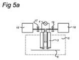
本発明の一実施形態は、処理空間の中で基板の表面に原子層を堆積する装置に関し、この装置は、処理空間に種々のガス混合物を供給するガス供給デバイスを含み、このガス供給デバイスは、基板の反応表面部位が前駆体材料分子と反応して、その反応部位を介して基板の表面に付着した前駆体分子の単分子層で覆われた表面を得ることができるように前駆体材料を含むガス混合物を処理空間に供給するように構成され、また、付着した前駆体分子を反応前駆体部位に変換できる反応剤を含むガス混合物を供給するように構成され、この装置はさらに、ガス混合物中に大気圧グロー放電プラズマを発生するプラズマ発生器を含み、このプラズマ発生器は、処理空間から離れて配置される。処理空間は、例えば処理チャンバである制御筐体、或いは、例えば基板ウェブの一部としての制御処理場所とすることができる。 One embodiment of the invention relates to an apparatus for depositing an atomic layer on a surface of a substrate in a processing space, the apparatus including a gas supply device that supplies various gas mixtures to the processing space, the gas supply device comprising: The precursor material so that the reaction surface part of the substrate can react with the precursor material molecules and the surface covered with a monolayer of precursor molecules attached to the surface of the substrate through the reaction part And a gas mixture containing a reactant capable of converting the deposited precursor molecules into reaction precursor sites, the apparatus further comprising a gas A plasma generator that generates an atmospheric pressure glow discharge plasma in the mixture is disposed away from the processing space. The processing space can be a control enclosure, for example a processing chamber, or a control processing location, for example as part of a substrate web.
一実施形態では、この装置は特に、本方法のステップB及びCを単一処理空間の中で実施するように設計される。このため、装置はさらに、動作時に基板が配置される第1の処理空間を含み、ガス供給デバイスはさらに、関連する方法の請求項のいずれか1つを実施するように構成される。 In one embodiment, the apparatus is specifically designed to perform steps B and C of the method in a single processing space. To this end, the apparatus further includes a first processing space in which the substrate is placed in operation, and the gas supply device is further configured to implement any one of the related method claims.
別の実施形態では、この装置は、1つがステップB用、1つがステップC用の2つの異なる処理空間を備えて設計される。この実施形態では、装置はさらに、前駆体材料を含むガス混合物に基板がさらされる第1の処理空間と、第2の処理空間であって、第2の処理空間から離れたプラズマ発生器内で生成され反応剤を含むガス混合物に基板がさらされる第2処理空間と、基板を第1と第2の処理空間の間で移動させる搬送デバイスとを含む。ガス供給デバイスは、過剰の反応物及び、又は形成された反応生成物を除去するフラッシングステップを含む、2つの処理空間を利用する上述した関連する方法の実施形態を適用するように構成することができる。 In another embodiment, the apparatus is designed with two different processing spaces, one for step B and one for step C. In this embodiment, the apparatus further includes a first processing space in which the substrate is exposed to a gas mixture including a precursor material, and a second processing space in a plasma generator remote from the second processing space. A second processing space in which the substrate is exposed to a gas mixture that is generated and that includes a reactant, and a transfer device that moves the substrate between the first and second processing spaces. The gas supply device may be configured to apply the related method embodiments described above that utilize two process spaces, including a flushing step to remove excess reactants and / or reaction products formed. it can.
さらに別の実施形態では、装置は、ステップB用及びステップC用の複数の連続した処理空間を有するように設計される。例えば、複数の第1及び第2の処理空間が、環状又は直線状の配列で順次後に1つずつ配置される。 In yet another embodiment, the apparatus is designed to have a plurality of consecutive processing spaces for Step B and Step C. For example, the plurality of first and second processing spaces are sequentially arranged one after another in an annular or linear array.
上記の装置実施形態は、連続的に移動するウェブ又は断続的に移動するウェブを基板が含むことができるように設計することができる。 The above device embodiments can be designed such that the substrate can include a continuously moving web or an intermittently moving web.
別の実施形態では、ガス供給デバイスは弁デバイスを備え、このガス供給デバイスは、弁デバイスを制御して種々のガス混合物を連続的又はパルス的に供給し、また過剰な材料及び反応生成物を不活性ガス又は不活性ガス混合物を使用して除去するように構成される。この弁デバイスは、1つ又は複数の弁を含むことができる。 In another embodiment, the gas supply device comprises a valve device that controls the valve device to supply various gas mixtures continuously or in a pulsed manner and to supply excess material and reaction products. It is configured to be removed using an inert gas or inert gas mixture. The valve device can include one or more valves.
さらに別の実施形態は、前駆体材料が基板表面近くに確実に保持されるように特に適合される。この目的のために、ガス供給デバイスは、基板の表面近くに配置された注入弁を有する注入チャネル(channel)を含み、導入チャネルを用いて基板の表面近くの第1層内にだけ、弁デバイス及び注入弁を制御して前駆体材料を連続的に供給するように、またガス混合物中の反応剤を不活性ガス又は不活性ガス混合物とともに第1層の上の第2層に連続的に導入するように構成される。 Yet another embodiment is particularly adapted to ensure that the precursor material is held near the substrate surface. For this purpose, the gas supply device comprises an injection channel with an injection valve arranged near the surface of the substrate, and only in the first layer near the surface of the substrate using the introduction channel, the valve device And control the injection valve to continuously supply the precursor material and continuously introduce the reactants in the gas mixture into the second layer above the first layer together with the inert gas or inert gas mixture. Configured to do.
別の実施形態では、プラズマ発生器は、パルス大気圧グロー放電プラズマを発生するように構成される。プラズマ発生器はさらに、プラズマ中の局所的不安定性に対抗するためにパルス大気圧グロー放電プラズマを安定化する安定化手段を含むことができる。 In another embodiment, the plasma generator is configured to generate a pulsed atmospheric pressure glow discharge plasma. The plasma generator may further include stabilizing means for stabilizing the pulsed atmospheric pressure glow discharge plasma to counter local instabilities in the plasma.
一実施形態では、プラズマ発生器の電極は、1対の平板として構成されるが、有利にはまた、複数対の平板電極のアレイを別の実施形態で使用することもできる。さらに別の実施形態では、電極は、内部電極を有する中空管電極として構成でき、或いは内部電極を有するそのような中空形電極のアレイとしてさえも構成することができる。また、上述の電極の組合せを有する実施形態を想定することもできる。 In one embodiment, the electrodes of the plasma generator are configured as a pair of plates, but advantageously also an array of multiple pairs of plate electrodes can be used in another embodiment. In yet another embodiment, the electrodes can be configured as hollow tube electrodes with internal electrodes, or even as an array of such hollow electrodes with internal electrodes. An embodiment having a combination of the above-described electrodes can also be envisaged.
さらに、この発明は、例えば基板上に材料の層を堆積するために、この発明の装置を使用することも対象とする。この基板は、例えば、(有機LED又は有機TFTの製造用などの)電子回路が上に設けられるべき合成基板とすることができる。基板は、例えばポリマー材料の、フレキシブル基板とすることができる。基板の厚さは重要ではなく、最大2cmまでさえも可能である。これらのタイプの基板は、本発明の実施形態を用いて処理するのに特に適しているのに対して、従来技術のシステム及び方法での処理は実用的ではなく、さらには不可能でもあった。或いは、このプラズマ堆積装置は、フレキシブル基板上にフレキシブル光起電力電池を製造するのに使用される。本発明はまた、本発明の装置及び方法を用いて堆積された原子層を備える基板にも関する。 Furthermore, the present invention is also directed to the use of the apparatus of the invention, for example to deposit a layer of material on a substrate. This substrate can be, for example, a synthetic substrate on which electronic circuits (such as for the production of organic LEDs or organic TFTs) are to be provided. The substrate can be a flexible substrate, for example of a polymer material. The thickness of the substrate is not critical and can even be up to 2 cm. While these types of substrates are particularly suitable for processing using embodiments of the present invention, processing with prior art systems and methods has been impractical and even impossible. . Alternatively, the plasma deposition apparatus is used to manufacture a flexible photovoltaic cell on a flexible substrate. The present invention also relates to a substrate comprising an atomic layer deposited using the apparatus and method of the present invention.
本発明を添付の図面を参照して以下でより詳細に説明する。 The present invention will be described in more detail below with reference to the accompanying drawings.
本発明によれば、基板から離れた大気圧プラズマの支援を用いた原子層堆積法(ALD)プロセス、即ち、いわゆる遠隔プラズマ支援ALDプロセスを実施するための改善された方法が提供される。ALDプロセスを使用して、Al2O3、HfO2、Ta2O5、及び他の多くの材料の原子層からなる欠陥のない被覆を堆積することができる。従来技術の方法では、一般に50ミリトールから10トールまでの低圧、及び/又は高温が、適切な作業工程のために必要である。The present invention provides an improved method for performing an atomic layer deposition (ALD) process with the assistance of atmospheric pressure plasma away from the substrate, ie, the so-called remote plasma assisted ALD process. An ALD process can be used to deposit defect free coatings consisting of atomic layers of Al2 O3 , HfO2 , Ta2 O5 and many other materials. In prior art methods, low pressures and / or high temperatures, typically from 50 mTorr to 10 Torr, are required for proper work processes.
化学気相成長法(CVD)及び物理気相成長法(PVD)とは異なり、原子層堆積法(ALD)は飽和表面反応に基づく。ALDプロセスの固有表面制御機構は、基板と前駆体分子の間の、個々の順次に行われる表面反応の飽和に基づく。この飽和機構では、膜成長速度が、CVD及びPVDにおけるように反応物濃度又は成長時間ではなく、反応サイクル数に直接比例するようになる。 Unlike chemical vapor deposition (CVD) and physical vapor deposition (PVD), atomic layer deposition (ALD) is based on a saturated surface reaction. The intrinsic surface control mechanism of the ALD process is based on saturation of individual sequential surface reactions between the substrate and precursor molecules. With this saturation mechanism, the film growth rate becomes directly proportional to the number of reaction cycles rather than the reactant concentration or growth time as in CVD and PVD.
ALDは自己制御式の反応プロセスであり、即ち、表面に付着される前駆体分子の量が、反応表面部位の数だけで決まり、飽和後の前駆体への露出とは無関係である。 ALD is a self-regulating reaction process, i.e., the amount of precursor molecules attached to the surface is determined solely by the number of reactive surface sites and is independent of exposure to the precursor after saturation.
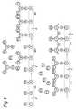
実際のALDサイクルは、図1に前駆体としてトリメチルアルミニウム(TMA)を用い、反応剤として水蒸気を用いる固定基板6の上へのAl2O3の例示的な原子層堆積で示されるように、4つのステップからなる。The actual ALD cycle is shown in FIG. 1 with an exemplary atomic layer deposition of Al2 O3 on a
ステップA:図1の(A)で示されるように、この場合には水酸基である反応表面部位をSi基板6の表面に形成することによって、原子層堆積用の表面6をコンディショニングする。 Step A: As shown in FIG. 1A, in this case, the
ステップB:前駆体投与。図1の(B1)で示されるように、このステップ中に前駆体分子(TMA)が反応表面部位と反応する。この結果、反応部位を介して基板6に付着した前駆体分子が、CH4など他のいくらかの揮発性反応生成物とともに生じる。これらの揮発性生成物は、ありうる過剰な材料とともに処理空間の外に除去され、理想的には、図1の(B2)で示されるように、前駆体の単分子層が基板6の表面に付着して残る。Step B: Precursor administration. As shown in FIG. 1 (B1), precursor molecules (TMA) react with reactive surface sites during this step. As a result, precursor molecules attached to the
ステップC:図1の(C1)で示されるように、反応剤(水蒸気)が基板6の表面近くに導入され、前駆体の単分子層と反応して所望の材料(Al2O3)の単分子層、及びいくらかの揮発性反応生成物(CH4など)が形成される。その表面には、Alに付着した水酸基の形で反応部位が並んだままである。図1の(C2)で示されるように、揮発性反応生成物、及びありうる未反応剤は除外される。Step C: As shown in FIG. 1 (C1), a reactant (water vapor) is introduced near the surface of the
任意選択で、ステップBとCのサイクルを繰り返して追加の単分子層を堆積する。各サイクルで1つの原子層を堆積することができ、これにより、膜厚及び膜特性の非常に正確な制御が可能になる。理論上、最大成長速度は、1サイクルあたりちょうど1単分子層であるが、ほとんどの場合、成長速度は、種々の理由により単分子層の0.2〜0.5、即ち0.25〜0.3に限定される。これらの理由の1つとして、吸収された前駆体分子による立体障害がありうる。 Optionally, repeat steps B and C to deposit additional monolayers. One atomic layer can be deposited in each cycle, which allows for very precise control of film thickness and film properties. Theoretically, the maximum growth rate is exactly one monolayer per cycle, but in most cases the growth rate is 0.2 to 0.5, or 0.25 to 0, of the monolayer for various reasons. .3. One of these reasons may be steric hindrance due to absorbed precursor molecules.
本発明によれば、反応剤を含む大気圧プラズマ中に基板から遠隔で生成されるガス混合物は、ステップCで、例えば、ガス混合物を基板に吹き付け又はパージすることによって基板に供給されて反応が実現する。ステップC中で、プラズマ中に生成されたガス混合物を用いてリガンド除去を促進し、これらを他の原子又は分子で置き換える。前駆体としてTMAを使用する上述の例示的な場合では、リガンドはメチル基で形成され、酸素原子及び水酸基で置き換えられる。これらの水酸基は、このプロセスサイクルを再びステップBから開始するのに適している。 According to the present invention, a gas mixture generated remotely from a substrate in an atmospheric pressure plasma containing a reactant is supplied to the substrate in step C, for example, by spraying or purging the gas mixture onto the substrate to react. Realize. In Step C, the gas mixture generated in the plasma is used to facilitate ligand removal and replace them with other atoms or molecules. In the exemplary case described above using TMA as a precursor, the ligand is formed with a methyl group and replaced with an oxygen atom and a hydroxyl group. These hydroxyl groups are suitable for starting the process cycle again from step B.
ALDプロセスは、標準的な低圧誘導結合プラズマ(ICP)又はRFプラズマが大気圧プラズマステップによって置き換えられることを除き、従来技術で説明されているように実施することができる。このため、関係するすべてのステップを今や大気圧のもとで実施することができる。 The ALD process can be performed as described in the prior art, except that a standard low pressure inductively coupled plasma (ICP) or RF plasma is replaced by an atmospheric pressure plasma step. For this reason, all relevant steps can now be carried out under atmospheric pressure.
本発明は有利なことに、基板6がポリマー箔など高温に耐えられない材料からなる場合に用いることができる。しかし、すべての種類の基板6が表面に活性部位を載せて使用可能であるので、本発明は、ポリマー箔に限定されない。基板6は、例えば、セラミック、ガラス、ウェハ、熱硬化性ポリマー及び熱可塑性ポリマーから選択できるが、また金属(細片)基板などから選択することもできる。 The present invention can advantageously be used when the
本発明の方法のステップAで、使用されるべき基板の表面には反応表面部位が形成されている。これは、例えばCVDステップによって行うことができる。このCVDステップ中、堆積は均一でなければならず、また基板表面を覆う活性部位の均一な分布が得られなければならない。図1の例では、これらの活性表面部位はSi−OH基である。これらのSi−OH基は、前駆体分子と反応するのに適している。しかし、本発明は、この特定の実施形態に限定されない。重要なことは、基板の表面が、前駆体分子と反応できる活性部位を含むことである。一実施形態では、このような表面活性部位は水酸基を含むが、別の実施形態では、活性表面部位はNH2基又はNHR基を含むことができ、ここでRは、短鎖の脂肪族基又は芳香族基とすることができる。これらの活性基は、Si、Ti、Al、Feなどのような種々の原子に結合することができる。さらに、P又はSを用いる活性部位を想定することもできる。In step A of the method of the invention, reactive surface sites are formed on the surface of the substrate to be used. This can be done, for example, by a CVD step. During this CVD step, the deposition must be uniform and a uniform distribution of active sites covering the substrate surface must be obtained. In the example of FIG. 1, these active surface sites are Si—OH groups. These Si-OH groups are suitable for reacting with precursor molecules. However, the present invention is not limited to this particular embodiment. Importantly, the surface of the substrate contains active sites that can react with the precursor molecules. In one embodiment, such surface active sites include hydroxyl groups, but in another embodiment, the active surface sites can include NH2 groups or NHR groups, where R is a short chain aliphatic group. Or it can be an aromatic group. These active groups can be bonded to various atoms such as Si, Ti, Al, Fe and the like. Furthermore, an active site using P or S can also be assumed.
ステップBで、基板の活性表面部位は前駆体分子と反応する。これらの前駆体分子は、有機金属化合物、並びに例えばハロゲン化物、又はハロゲン化物と有機リガンドの両方を含む物質から選択することができる。これらの前駆体の元素は、例えば、コバルト、銅、クロム、鉄、アルミニウム、ヒ素、バリウム、ベリリウム、ビスマス、ホウ素、ニッケル、ガリウム、ゲルマニウム、金、ハフニウム、鉛、マグネシウム、マンガン、水銀、モリブデン、ニオブ、オスミウム、リン、白金、ルテニウム、アンチモン、シリコン、銀、硫黄、タンタル、スズ、チタン、タングステン、バナジウム、亜鉛、イットリウム、ジルコニウムなどから選択することができる。複数の元素を含む前駆体分子もまた使用することができる。これらの分子の例は、
ビス(N,N’−ジイソプロピルアセトアミジナート)コバルト(II)、(N,N’−ジ−sec−ブチルアセトアミジナート)銅(I)、(N,N’−ジイソプロピルアセトアミジナート)銅(I)、ビス(N,N’−ジ−tert−ブチルアセトアミジナート)鉄(II)、ビス(N,N’ジイソプロピルアセトアミジナート)ニッケル(II)、アルミニウムsec−ブトキシド、ジエチルアルミニウムエトキシド、トリメチルアルミニウムトリス(ジエチルアミド)アルミニウム、トリス(エチルメチルアミド)アルミニウム、ジボラン(水素中10%)、トリメチルホウ素、トリメチルガリウム、トリス(ジメチルアミド)アルミニウム、ジゲルマン(H2中10%)、テトラメチルゲルマニウム、塩化ハフニウム(IV)、ハフニウム(IV)tert−ブトキシド、テトラキス(ジエチルアミド)ハフニウム(IV)、テトラキス(ジメチルアミド)ハフニウム(IV)、テトラキス(エチルメチルアミド)ハフニウム(IV)、ビス(シクロペンタジエニル)マグネシウム(II)、ビス(ペンタメチルシクロペンタジエニル)マグネシウム(II)、ビス(エチルシクロペンタジエニル)マンガン、ヘキサカルボニルモリブデン、ニオブ(V)エトキシド、ビス(メチルシクロペンタジエニル)ニッケル(II)、ビス(エチルシクロペンタジエニル)マグネシウム(II)、シクロペンタジエニル(トリメチル)白金(IV)、ビス(エチルシクロペンタジエニル)ルテニウム(II)、トリス(ジメチルアミド)アンチモン、2,4,6,8−テトラメチルシクロテトラシロキサン、ジメトキシジメチルシラン、ジシラン、メチルシラン、オクタメチルシクロテトラシロキサン、シラン、トリス(イソプロポキシ)シラノール、トリス(tert−ブチオキシ)シラノール、トリス(tert−ペントキシ)シラノール、ペンタキス(ジメチルアミド)タンタル(V)、トリス(ジエチルアミド)(tert−ブチルイミド)タンタル(V)、ビス(ジエチルアミノ)ビス(ジイソプロピルアミノ)チタン(IV)、テトラキス(ジエチルアミド)チタン(IV)、テトラキス(ジメチルアミド)チタン(IV)、テトラキス(エチルメチルアミド)チタン(IV)、ビス(tert−ブチルイミド)ビス(ジメチルアミド)タングステン(VI)、タングステンヘキサカルボニル、トリス(N,N−ビス(トリメチルシリル)アミド)イットリウム(III)、ジエチル亜鉛、テトラキス(ジエチルアミド)ジルコニウム(IV)、テトラキス(ジメチルアミド)ジルコニウム(IV)、テトラキス(エチルメチルアミド)ジルコニウム(IV)がある。前駆体分子としては、SiCl2H2、SiCl3H、SiClH3、SiCl4、TiCl4、TICl3H、TiCl2H2及びTiCLH3が好ましい。In step B, the active surface site of the substrate reacts with the precursor molecules. These precursor molecules can be selected from organometallic compounds, as well as substances containing, for example, halides or both halides and organic ligands. These precursor elements include, for example, cobalt, copper, chromium, iron, aluminum, arsenic, barium, beryllium, bismuth, boron, nickel, gallium, germanium, gold, hafnium, lead, magnesium, manganese, mercury, molybdenum, It can be selected from niobium, osmium, phosphorus, platinum, ruthenium, antimony, silicon, silver, sulfur, tantalum, tin, titanium, tungsten, vanadium, zinc, yttrium, zirconium and the like. Precursor molecules containing multiple elements can also be used. Examples of these molecules are
Bis (N, N′-diisopropylacetamidinato) cobalt (II), (N, N′-di-sec-butylacetamidinato) copper (I), (N, N′-diisopropylacetamidinato) ) Copper (I), bis (N, N′-di-tert-butylacetamidinato) iron (II), bis (N, N′diisopropylacetamidinato) nickel (II), aluminum sec-butoxide, diethylaluminum ethoxide, tri-methyl aluminum tris (diethylamide) aluminum, tris (ethylmethylamido) aluminum, diborane (10% in hydrogen), trimethylboron, trimethyl gallium, tris (dimethylamide) aluminum, digermane (10%H 2) , Tetramethylgermanium, hafnium (IV) chloride, hafniu (IV) tert-butoxide, tetrakis (diethylamide) hafnium (IV), tetrakis (dimethylamido) hafnium (IV), tetrakis (ethylmethylamido) hafnium (IV), bis (cyclopentadienyl) magnesium (II), bis (Pentamethylcyclopentadienyl) magnesium (II), bis (ethylcyclopentadienyl) manganese, hexacarbonylmolybdenum, niobium (V) ethoxide, bis (methylcyclopentadienyl) nickel (II), bis (ethylcyclo Pentadienyl) magnesium (II), cyclopentadienyl (trimethyl) platinum (IV), bis (ethylcyclopentadienyl) ruthenium (II), tris (dimethylamido) antimony, 2,4,6,8-tetra Methylsiku Tetrasiloxane, dimethoxydimethylsilane, disilane, methylsilane, octamethylcyclotetrasiloxane, silane, tris (isopropoxy) silanol, tris (tert-butoxy) silanol, tris (tert-pentoxy) silanol, pentakis (dimethylamido) tantalum (V ), Tris (diethylamide) (tert-butylimido) tantalum (V), bis (diethylamino) bis (diisopropylamino) titanium (IV), tetrakis (diethylamido) titanium (IV), tetrakis (dimethylamido) titanium (IV), tetrakis (Ethylmethylamido) titanium (IV), bis (tert-butylimido) bis (dimethylamido) tungsten (VI), tungsten hexacarbonyl, tris (N, N-bi-) Su (trimethylsilyl) amido) yttrium (III), diethylzinc, tetrakis (diethylamido) zirconium (IV), tetrakis (dimethylamido) zirconium (IV), tetrakis (ethylmethylamido) zirconium (IV). As precursor molecules, SiCl2 H2 , SiCl3 H, SiClH3 , SiCl4 , TiCl4 , TICl3 H, TiCl2 H2 and TiCLH3 are preferred.
これらの化合物の混合物もまた使用することができる。 Mixtures of these compounds can also be used.
このステップBは、処理空間5(例えば図5aの記載参照)の中で行うことができ、そこでは反応部位を有する基板6が固定位置に配置され移動しない。前駆体は、この処理空間5内に挿入され、その後、反応表面部位との反応が起こる。前駆体は、不活性キャリアガスによって付加される。この不活性キャリアガスは、希ガス及び窒素から選択することができる。不活性ガス混合物もまたキャリアガスとして使用することができる。キャリアガス中の前駆体の濃度は、10から5000ppmまでとすることができるが、表面反応を完了させるのに十分でなければならない。反応は、ほとんどの場合で瞬時である。活性表面部位と前駆体の間の反応が完了した後、処理空間5は、不活性ガス又は不活性ガス混合物でパージされ、又はフラッシングされ、この不活性ガス又は不活性ガス混合物は、前駆体のキャリアガスとして使用される同じガス又はガス混合物でよいが、異なるガス又はガス混合物でもよい。ステップBは、室温で行うのが最も好ましいが、また高温で実施することもできる。しかし、どんな場合でも基板が劣化し始める温度よりは十分に低くなければならない。ポリエチレンのようなプラスチックでは、温度は例えば80℃より下にとどまることが好ましいが、例えばウェハ、ガラス又はセラミックでは、温度は必要に応じて100℃を超えてもよい。前駆体分子を備えた基板6は、次のステップまで保管することができ、或いはただちに次のステップにかけることもできる。 This step B can be performed in the processing space 5 (see, for example, the description of FIG. 5a), in which the
一般には、ALDプロセスのステップCは、高温において大気圧未満で行われる。このステップで、活性表面部位を介して基板6に付着した前駆体分子は、付着前駆体と反応剤との熱反応、或いは低圧誘導結合プラズマ又は低圧RFプラズマによって増強された熱反応などの熱反応の後に前駆体分子に由来して形成される化合物の単分子層に変換される。したがって従来技術では、ステップCは一般に、別の堆積ステップBに適した活性部位を有する化合物の単分子層へと前駆体分子を完全に変換するために、高温即ち100℃を超える温度において低圧で実施される。前述のように、従来技術の方法を用いると、その加熱ステップの故に、ガラス温度Tgが比較的低い、膨大な数の熱可塑性ポリマーを基板6として使用することが不可能になる。 In general, step C of the ALD process is performed at elevated temperatures and below atmospheric pressure. In this step, the precursor molecules attached to the
本発明者らは驚くべきことに、あまり高くない温度において大気圧で、ステップCを大気圧プラズマ及び高電界を用いて実施できることを今では発見しており、この場合プラズマは、基板6から離れた電極間で、反応剤と不活性ガス又は不活性ガス混合物とのガス混合物中で発生される。不活性ガスは、希ガス及び窒素から選択することができる。不活性ガス混合物は、希ガスの混合物又は希ガスと窒素の混合物とすることができる。ガス又はガス混合物中の反応剤の濃度は、1%から50%までとすることができる。反応剤は基本的に、ステップBで、活性部位を介して基板6に付着される前駆体分子のリガンドと反応する。この反応剤は、酸素、或いはオゾン、水、酸化炭素又は二酸化炭素のような酸素含有ガスとすることができる。反応剤はまた、窒素、或いはアンモニア、一酸化窒素、一酸化二窒素、二酸化窒素などの窒素含有化合物を含むこともできる。 The inventors have now surprisingly discovered that step C can be carried out using atmospheric pressure plasma and a high electric field at atmospheric pressure at moderate temperatures, in which case the plasma is separated from the
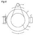
一般に、大気圧プラズマは、2つの電極間に発生される。プラズマ発生器10の電極は、図5aの実施形態に示されるように、電源4に接続された1対の平板3として構成でき、さらには図5bの実施形態に示されるように、単一の電源4に接続された各平板からなる複数対の電極のアレイとしても構成することができる。別の実施形態では、電極は、内部電極を有する中空管電極の組合せとして構成でき、さらには内部電極を有するそのような中空形電極のアレイとしても構成することができ、この場合ガス混合物は、中空管電極(単数又は複数)の内側でプラズマにさらされる。 In general, atmospheric pressure plasma is generated between two electrodes. The electrodes of the
大気圧プラズマは、当技術分野で知られているこのプラズマのどんな種類でもよい。非常に良好な結果が、パルス大気圧グロー放電(APG)プラズマを使用して得られる。最近までこれらのプラズマは安定性がよくなかったが、例えば米国特許第6774569号、EP−A−1383359、EP−A−1547123及びEP−A−1626613に記載されている安定化手段を用いて、非常に安定したAPGプラズマを得ることができる。一般に、これらのプラズマは、プラズマ中の局所的不安定性に対抗する安定化手段によって安定化される。 The atmospheric pressure plasma can be any type of this plasma known in the art. Very good results are obtained using a pulsed atmospheric pressure glow discharge (APG) plasma. Until recently, these plasmas were not stable, but for example, using the stabilizing means described in US Pat. No. 6,774,569, EP-A-1383359, EP-A-1547123 and EP-A-1626613, A very stable APG plasma can be obtained. In general, these plasmas are stabilized by stabilizing means that counteract local instabilities in the plasma.
ステップCの後、ステップCで形成された化合物の単分子層を備えた基板が得られる。この単分子層は、その順番で再び、繰返しステップB及びCに適した活性部位を得て、それによって、基板に複数の単分子層を互いの上に付けることができ、10層、20層、50層、100層、さらには200層もの多くの層を互いの上に付けることができる。 After step C, a substrate with a monolayer of the compound formed in step C is obtained. This monolayer again obtains active sites suitable for repeated steps B and C in that order, whereby a plurality of monolayers can be applied on top of each other on the substrate. As many as 50, 100, or even 200 layers can be applied on top of each other.
ある特定のサイクルにおいて前駆体を変更することによって、異なる組成の単分子層を互いの上に付けることができ、それによって、非常に特殊な特性を得ることができる。 By changing the precursor in a certain cycle, monolayers of different composition can be applied on top of each other, thereby obtaining very specific properties.
本発明のALD法の各ステップを実行する種々の実施形態がある。 There are various embodiments for performing each step of the ALD method of the present invention.
一実施形態では、各ステップは、単一の処理空間5内で実施される(例えば、図5aを参照して説明する以下の実施形態を参照)。この実施形態で、基板6は、処理空間5内の固定位置にある。ステップBの前駆体分子の堆積中には、基板6は固定位置にあってよく、ステップCの大気圧プラズマによる処理中には、基板6は固定位置にあってもよいが、ある線形速度を有してもよい。 In one embodiment, each step is performed within a single processing space 5 (see, for example, the following embodiment described with reference to FIG. 5a). In this embodiment, the
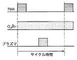
満足な単分子層堆積法を得るには、ガス流を制御する方法を有することが重要である。一実施形態では、前駆体を含むガス混合物が処理空間5に付加され反応が完了した後、処理空間は不活性ガス(混合物)でフラッシングされる。この後、活性ガスを含む不活性ガス(混合物)が、基板6から離れたプラズマ発生器10の電極3の間に挿入され、プラズマの点火後に、例えばガス混合物を処理空間5に吹き付ける、又はパージすることによって基板6に供給される。基板6は、ある線形速度で処理空間5中を移動させることができる。この処理の後、処理空間5は再び不活性ガス(混合物)でフラッシングされ、ステップB及びCは、所望の数の単分子層が得られるまで繰り返すことができる。この方法では、前駆体材料はガス(混合物)中にパルス的に供給され、反応剤は、不活性ガス又は不活性ガス混合物とともにガス混合物中にやはりパルス的に導入され、この方法はさらに、前駆体材料の各パルス的供給、及び反応剤のパルス的導入の後に、過剰な材料及び反応生成物を不活性ガス又は不活性ガス混合物を用いて除去することも含む。これは、一実施形態として図2に概略的に示されており、この場合、TMAは前駆体として、アルゴンはフラッシングガスとして、酸素は反応剤として使用されている。 In order to obtain a satisfactory monolayer deposition method, it is important to have a method for controlling the gas flow. In one embodiment, after the gas mixture containing the precursor is added to the processing space 5 and the reaction is complete, the processing space is flushed with an inert gas (mixture). Thereafter, an inert gas (mixture) containing an active gas is inserted between the
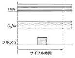
別の実施形態では(図3のタイミング図に概略的に示す)、前駆体材料(この例ではTMA)は不活性ガスとともにガス混合物中にパルス的に供給され、反応剤(酸素)は不活性ガス混合物中に(アルゴンとともに)連続的に供給され、即ち、処理空間5に挿入されるガス混合物は反応剤を継続的に含み、前駆体は不連続的に付加されることになる。この実施形態は、前駆体と反応剤が気相で互いに反応しない、又は実質的に反応しない場合に実現可能である。この実施形態では、ガス供給法が第1の実施形態よりもいくらか簡単である。この方法では、過剰な材料及び反応生成物は、前駆体材料の各パルス的供給及び放電プラズマのパルス的印加の後に、反応剤を含む不活性ガス又は不活性ガス混合物を使用して処理空間からパージされる。 In another embodiment (shown schematically in the timing diagram of FIG. 3), the precursor material (TMA in this example) is pulsed into the gas mixture with an inert gas and the reactant (oxygen) is inert. The gas mixture that is continuously fed into the gas mixture (with argon), that is, the gas mixture that is inserted into the processing space 5, will continuously contain the reactants and the precursor will be added discontinuously. This embodiment is feasible when the precursor and the reactant do not react or do not substantially react with each other in the gas phase. In this embodiment, the gas supply method is somewhat simpler than in the first embodiment. In this method, excess material and reaction products are removed from the processing space using an inert gas or inert gas mixture containing a reactant after each pulsed supply of precursor material and pulsed application of a discharge plasma. Purged.
さらに別の実施形態では、図4のタイミング図で示されるように、前駆体材料(TMA)は不活性ガス混合物中で、基板の表面近くの第1層だけに連続的に供給され、反応剤(酸素)はガス混合物中で、基板6から離れた大気圧プラズマ中に不活性ガス(アルゴン)とともに導入され、且つ第1層の上の第2層に連続的に供給される。この実施形態では、層流が必要条件である。この実施形態は、有利には、前駆体と反応剤が互いに反応しない、又は実質的に反応しない場合に適用される。やはり大気圧プラズマ処理がパルス的に行われ、それによって、この方法は、前駆体が活性表面部位と反応することを可能にするプラズマオフ時間と、表面に付着した前駆体分子が必要な化学物質に変換されるプラズマオン時間とを含む。この実施形態では、種々のガス混合物の組成はプロセス中に変化しないが、層流を得るための流れの制御が重要である。 In yet another embodiment, as shown in the timing diagram of FIG. 4, precursor material (TMA) is continuously fed only in the inert gas mixture to the first layer near the surface of the substrate and the reactants. (Oxygen) is introduced together with an inert gas (argon) into the atmospheric plasma away from the
上述した実施形態はすべて、1つの処理空間5が使用可能の場合に適用可能である。この方法はまた、少なくとも2つの処理空間1、2を使用する場合に適用することもでき、その場合、第1処理空間1は前駆体と活性表面部位との反応で使用され、第2処理空間2は、大気圧プラズマ処理で使用される(以下で説明する図5b及び図6の実施形態を参照)。この実施形態では、ガス組成及びガス流の制御がより簡単であり、より高い効率を得ることができる。この実施形態では、基板6は、処理空間1及び2を連続的に通して移動される。プラズマ処理ステップで起こる関連の反応が非常に速いので、1m/分の移動速度がかなり一般的であるが、10m/分のようなより速い速度を用いることもでき、特別な場合では100m/分と同程度の速い速度を用いることもできる。この実施形態では、ガス流は連続的のものにすることができ、処理空間1には前駆体を含む不活性ガス(混合物)が挿入され、処理空間2にはガス(混合物)が反応剤を含めてプラズマ発生器10から供給される。この実施形態のさらなる利点は、第1処理空間1の中の温度と第2処理空間2の中の温度とが同じである必要がないことであるが、ポリマー基板の場合には、温度は、好ましくはそのガラス転移温度未満でなければならず、あるポリマー基板では100℃未満でありうるが、処理空間1、2の両方で100℃を超えることもまたありうる。さらに別の実施形態では(図5bの記載参照)、基板6は、連続的ではなく断続的に一方の処理空間から他方へと移動し、処理中には移動していない。 All the above-described embodiments are applicable when one processing space 5 is usable. This method can also be applied when using at least two
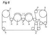
さらに別の実施形態では、処理空間1及び2と、処理されるべき基板6とはループを形成し、それによって連続するステップBとステップCは、原理的には無限に繰り返すことができる。この実施形態の実施が、図6及び図8に概略的に示されており、これを以下でより詳細に説明する。 In yet another embodiment, the
さらに別の実施形態では、複数の第1処理空間1及び第2処理空間2が互いの後に配置される。この実施形態では、連続プロセスを用いて、同じ組成又は異なる組成の種々の単分子層を互いの上に付けることができる。第1処理空間1及び第2処理空間2の配置については、すべての場合でプラズマ発生器10が実際の処理空間2の外側に設けられること、及び供給手段が、反応剤を含むガス混合物をプラズマ発生器10から処理空間2まで導くように設けられることを除いて、厳格な要件がない。処理空間1、2は、直線状、環状、又は連続プロセスに適した他の任意の配置で構成することができる。 In yet another embodiment, a plurality of first processing spaces 1 and
さらに別の大気圧未満での実施形態では、例えば1トール、或いは10、20又は30トールの圧力でプラズマを使用することができる。 In still other sub-atmospheric embodiments, the plasma can be used at a pressure of, for example, 1 Torr, or 10, 20, or 30 Torr.
さらに別の実施形態では、処理空間1と2は分離され、即ち、まず処理空間1の中で前駆体分子が基板6の活性部位に付着され、この修飾された基板6は、この基板6が安定な条件下で保管され、別の時間に処理空間2の中で処理され、遠隔のプラズマ発生器10で生成されたガス混合物による処理を受ける。 In yet another embodiment,
本発明はまた、本発明の方法を実施するように構成された装置も対象とする。 The present invention is also directed to an apparatus configured to perform the method of the present invention.
図5aに概略的に示されている一実施形態では、この装置は処理空間5と、処理空間5から離れた2つの電極3の間で大気圧プラズマを発生するプラズマ発生器10とを含む。電極3は、図5aに太線で示された誘電体バリアを備えることができる。この装置はさらに、第1ガス供給源15及び第2ガス供給源16を含む。この実施形態で使用される種々の構成要素(前駆体、反応剤、不活性ガス(混合物))は、第1ガス供給手段15及び第2ガス供給手段16と、付随する弁17、18とを使用して電極3の間の空間に注入される。第1ガス供給源15は、前駆体及び不活性ガスを供給するように構成することができ、第2ガス供給源16は、反応剤及び不活性ガスを供給するように構成することができる。 In one embodiment schematically illustrated in FIG. 5 a, the apparatus includes a processing space 5 and a
第1ガス供給手段15と第2ガス供給手段16は、単一のガス供給デバイスとして組み合わせることができ、このデバイスは、種々のガス容器を含むことができ、混合手段を備え、この混合手段は、種々のガス成分を均一に正確に混合すること、成分が異なる種々の混合物を同時に供給すること、或いは種々のガス混合物を順次に供給することができ、また長時間にわたり安定したガス流を維持することができる。 The first gas supply means 15 and the second gas supply means 16 can be combined as a single gas supply device, which can include various gas containers and comprises a mixing means, the mixing means comprising Can mix various gas components uniformly and accurately, supply various mixtures with different components at the same time, or supply various gas mixtures sequentially, and maintain stable gas flow for a long time can do.
図5aに概略的に示される第1ガス供給手段15及び第2ガス供給手段16は、実際には、前駆体、反応ガス、パージガスをパルス化によりプロセスに供給できる2つ又は3つ以上の出口を有するガスシャワーヘッドからなる。しかし、完全に混合することが堆積物の均一性にとっては重要である。 The first gas supply means 15 and the second gas supply means 16 shown schematically in FIG. 5a are actually two or more outlets through which precursors, reaction gases and purge gases can be supplied to the process by pulsing. A gas shower head having However, thorough mixing is important for deposit uniformity.
この設備では、高速切替弁17、18が、上述した図2及び図3の実施形態の場合に使用され、そこでは1つ又は複数のガス流がパルス的に供給される。したがって、例えば図2に示されたプロセスでは、種々のガス混合物を同時に調製することができ、即ち、ガス付加のシーケンスは、1つ(1組)の弁(単数又は複数)17によって制御される。したがって、ステップBを実行するとき、弁17が、前駆体を含むガス混合物の方に切り替えられて前駆体を含むガスパルスが与えられ、このパルスの後、この弁17(又は別の弁17)は、パージ用の不活性ガス組成物の方に切り替えられ、この後、弁18が、反応剤を含むガス組成物の方に切り替えられて、ステップCが実行される。最終ステップとして、弁18は、もう1つのパージステップのために不活性ガス組成の方に切り替えられる。弁17、18は、当業者にはそのようなものとして知られており、したがってこれ以上詳細には説明しないが、混合を防止し、ガス流の遅延時間を短縮するために、処理空間5に可能な限り近接して取り付けられる。拡散によるガス混合を制限するには、かなり高いガス流が必要である(即ち>1m/秒)。さらに、上述したように、図5aに示された実施形態での前駆体注入は、前駆体の流れを限定し拡散を制限するために、基板6の表面に可能な限り近くなければならない。これは、電極3からの流出開口を基板6に可能な限り近接して配置することによって達成することができる。別法として、第1ガス供給源15の流出部を基板6に近接して配置することもできる。このようにしてALDモードを維持することができる。 In this installation, fast switching valves 17, 18 are used in the case of the embodiments of FIGS. 2 and 3 described above, in which one or more gas flows are pulsed. Thus, for example, in the process shown in FIG. 2, various gas mixtures can be prepared simultaneously, ie, the sequence of gas addition is controlled by one (a set) of valve (s) 17. . Thus, when performing step B, the valve 17 is switched towards the gas mixture containing the precursor to give a gas pulse containing the precursor, after which this valve 17 (or another valve 17) is The inert gas composition for purging is switched to, and then the valve 18 is switched to the gas composition containing the reactant, and Step C is performed. As a final step, the valve 18 is switched towards the inert gas composition for another purge step. Valves 17 and 18 are known as such to those skilled in the art and therefore will not be described in further detail, but in order to prevent mixing and reduce gas flow delay time in the processing space 5. Install as close as possible. To limit gas mixing by diffusion, a fairly high gas flow is required (ie> 1 m / sec). Furthermore, as described above, the precursor implantation in the embodiment shown in FIG. 5a must be as close as possible to the surface of the
任意選択の機能として、この装置は、ある線形速度で基板6を処理空間5に通して移動させる移動手段を、例えば搬送機構の形で備えることができる。 As an optional function, the apparatus can comprise moving means for moving the
図5bに概略的に示された別の実施形態では、この装置は、種々のガス混合物を処理空間1に供給するためのガス供給手段15を備えた第1処理空間1を含む。ガス混合物は、前駆体と不活性ガス又は不活性ガス混合物、或いは不活性ガス又は不活性ガス混合物を含むことができる。ガス供給手段15は、種々のガス容器を含むことができ、またガス供給手段15は混合手段を含むことができ、この混合手段は、種々のガス成分を均一に正確に混合すること、成分が異なる種々の混合物を同時に供給すること、或いは別々のガス混合物を順次に供給することができ、また長時間にわたり安定したガス流を維持することができる。ガス付加のシーケンスは、1つ(1組)の弁(単数又は複数)17によって制御することができる。したがって、本発明のステップBを処理空間1の中で実行するとき、弁17が、前駆体を含むガス混合物の方に切り替えられて前駆体材料を含むガスパルスが得られ、このパルスの後、この弁17、又は別の弁(図示せず)が、パージ用の不活性ガス組成物の方に切り替えられる。さらに、この実施形態の装置は、大気圧プラズマを発生するプラズマ発生器10と、付随する弁18を使用して種々のガス混合物を第2処理空間2に供給する第2ガス供給源16とを備える第2処理空間2を含む。ガス混合物は、反応剤と不活性ガス又は不活性ガス混合物との混合物、或いは不活性ガス又は不活性ガス混合物を含む。第2ガス供給手段もやはり、種々のガス容器、及び混合手段を含むことができ、この混合手段は、種々のガス成分を均一に正確に混合すること、成分が異なる種々の混合物を同時に供給すること、或いは種々のガス混合物を順次に供給することができ、また長時間にわたり安定したガス流を維持することができる。処理空間2でもまた、ガス付加のシーケンスは、1つ(1組)の弁(単数又は複数)18によって制御することができる。基板6が第2処理空間2に入った後、弁18は、反応剤を含むガス混合物の方に切り替えられて、大気圧放電プラズマを点火することによってステップCが実行され、最終ステップとして弁18は、パージステップのために不活性ガス組成物の方に切り替えられる。この装置はさらに、基板6を第1処理空間1から第2処理空間2まで移動させるための、例えば搬送ロボットの形の搬送手段20を含む。 In another embodiment schematically shown in FIG. 5 b, the apparatus comprises a first processing space 1 with gas supply means 15 for supplying various gas mixtures to the processing space 1. The gas mixture can include a precursor and an inert gas or inert gas mixture, or an inert gas or inert gas mixture. The gas supply means 15 can include various gas containers, and the gas supply means 15 can include a mixing means. The mixing means can mix various gas components uniformly and accurately. Different different mixtures can be fed simultaneously, or separate gas mixtures can be fed sequentially, and a stable gas flow can be maintained over a long period of time. The sequence of gas addition can be controlled by one (a set) of valve (s) 17. Thus, when step B of the present invention is performed in the processing space 1, the valve 17 is switched towards the gas mixture containing the precursor to obtain a gas pulse containing the precursor material, after which this pulse Valve 17 or another valve (not shown) is switched to the inert gas composition for purging. Furthermore, the apparatus of this embodiment includes a
図5a及び5bに示される上記の実施形態は、以下の共通の要素を有する。処理空間1;2、5の中で基板6の表面に原子層を堆積する装置は、種々のガス混合物を処理空間1;2、5に供給するガス供給デバイス15、16を含み、ガス供給デバイス15、16は、前駆体材料を含むガス混合物を処理空間1;2、5に供給するように構成されて、反応表面部位が前駆体材料分子と反応して、その反応部位を介して基板6の表面に付着した前駆体分子の単分子層で覆われた表面を得ることができる。続いて、付着した前駆体分子を活性前駆体部位に変換できる反応剤を含むガス混合物が供給され、装置はさらに、反応剤を含むガス混合物中に大気圧プラズマを発生するプラズマ発生器10を含む。さらに、ガス供給デバイス15、16は、弁デバイス17、18を備え、このガス供給デバイス15、16は、弁デバイス17、18を制御して種々のガス混合物を連続的又はパルス的に供給し、また過剰な材料及び反応生成物を不活性ガス又は不活性ガス混合物を使用して除去するように構成される。 The above embodiment shown in FIGS. 5a and 5b has the following common elements: The apparatus for depositing an atomic layer on the surface of the
一代替実施形態では、第1ガス供給デバイス15は、弁17を有する注入チャネルを含むことができ、この注入チャネルは基板6の表面近くに配置され、ガス供給デバイス15は、注入チャネルを用いて基板6の表面近くの第1層にだけ、弁17を制御して前駆体材料を連続的に供給するように構成される。その場合、第2ガス供給源16は、ガス混合物中の反応剤を不活性ガス又は不活性ガス混合物とともに第1層の上の第2層に連続的に導入するように構成される。 In an alternative embodiment, the first
この装置の別の代替実施形態では、搬送手段20は、ある線形速度で基板6を連続的に、又は断続的に第1処理空間1から第2処理空間2まで(本発明のステップBとCを繰り返すことに関し、逆も同様である)移動させるように構成される。 In another alternative embodiment of the apparatus, the transport means 20 moves the
図5a及び5bに示された実施形態の主要な各要素が交換できること、即ち、図5aの実施形態に図5bの複数電極構成を使用でき、図5bの実施形態に単一対の電極3を使用できることは明らかであろう。 The main elements of the embodiment shown in FIGS. 5a and 5b can be interchanged, ie the embodiment of FIG. 5a can use the multi-electrode configuration of FIG. 5b and the embodiment of FIG. 5b uses a single pair of
図6に、基板6が無限ウェブ基板の形で供給される別の装置実施形態が概略的に示されている。この装置は、2つの主駆動シリンダ31、32を含み、これらはテンションローラ33、並びに処理ローラ34及び35を介して基板6を駆動する。処理ローラ34は、本発明のステップBを実施する第1処理空間1に沿って基板6を駆動し、処理ローラ35は、本発明のステップCを実施する第2処理空間2に沿って基板6を駆動する。この実施形態で、第2処理空間2もやはり、基板6を損傷しないように、付随するプラズマ発生器10から離れている。 FIG. 6 schematically shows another apparatus embodiment in which the
別の装置実施形態では、基板6は、図8に示されるように、回転できるシリンダ51のまわりに巻き付けられる。シリンダ51を回転させると、基板6は処理空間1を通過して本発明のステップBが実施され、さらに回転させると、基板6は処理空間2を通過して本発明のステップCが実施される。やはり、処理空間2には遠隔に配置されたプラズマ発生器10が付随し、その例は図5a及び5bに示されている。この実施形態では、原子層の連続堆積を実施することができる。シリンダ52の駆動は、図8に示されるように、シリンダ52に接続された駆動シャフト52を駆動するモータ53を使用して実施することができる。基板6を洗うことは、シリンダ52のまわりに処理空間1又は2が存在しない、図8の参照数字50で示されるステージで行うことができる。 In another apparatus embodiment, the
さらに別の装置実施形態では、装置は、図7a、7b及び7cに概略的に示された種々の実施形態に示されるように、連続する第1処理空間1と第2処理空間2(又は別法として処理空間47)で構成される。やはり、第2処理空間2(又は処理空間47)は、基板6から離れて配置されたプラズマ発生器10を備える。これらの実施形態では、ウェブなどの形の基板6が、巻戻しローラ41から巻取りローラ42まで給送される。巻戻しローラ41と巻取りローラ42の間に、いくつかのテンションローラ46が配置される。これにより、連続する第1処理空間1と第2処理空間2の中で、基板6を線形速度で連続的に、又は断続的に移動させることができる。任意選択で、種々の処理空間1、2は、限定された領域内に前駆体及び反応剤を保持するためのロックを備える。この実施形態の装置は、フレキシブル基板の上に種々の層を堆積するのに非常に適しており、処理されるべき基板6は、巻戻しローラ41から巻き戻され、処理された基板6は、巻取りローラ42上に再び巻き付けられる。 In yet another apparatus embodiment, the apparatus comprises a continuous first process space 1 and second process space 2 (or another, as shown in the various embodiments schematically illustrated in FIGS. 7a, 7b and 7c. It is constituted by a processing space 47). Again, the second processing space 2 (or processing space 47) includes the
図7aに示される代替実施形態では、基板6はまず、前処理空間45の中で処理されて、例えば、上述した本発明による第1前処理ステップAを実行する。次に、基板6は、テンションローラ46に沿って第1処理シーケンス(sequence)ローラ43まで移動する。第1処理シーケンスローラ43の外周に沿って、連続する第1処理空間1と第2処理空間2が図示の実施形態では2対配置され、これにより基板6の上に2つの原子層を形成することができる。次に、基板6は、別のテンションローラ46に沿って、やはり連続した第1処理空間1と第2処理空間2を備える別の処理シーケンスローラ44(さらには複数の別の処理シーケンスローラ44)まで移動される。 In an alternative embodiment shown in FIG. 7a, the
図7bに、一代替構成が概略的に示されている。巻戻しローラ41と巻取りローラ42の間に、多数のテンションローラ46が設けられる。第1テンションローラ46の外周部に前処理空間45が設けられ、この中で基板6に対して本発明のステップAが適用される。別のテンションローラ46に処理空間47を設けることができ、ここで基板6に対してステップBとCの両方が適用される。一代替形態として、後続の処理空間47は、ステップBとステップCを交互に適用するように構成することができる。 In FIG. 7b, an alternative configuration is schematically shown. A number of
図7cに、さらに別の代替構成が概略的に示されている。巻戻しローラ41と巻取りローラ42の間に、いくつかのテンションローラ46が設けられる。2つのテンションローラ46の間に第1処理空間1又は第2処理空間2が、本発明のステップBとステップCを交互に適用するように設けられる。 In FIG. 7c, yet another alternative configuration is schematically shown.
この装置実施形態で使用されるプラズマは、連続波プラズマが好ましい。より好ましいプラズマは、パルス大気圧放電プラズマ、又はパルス大気圧グロー放電プラズマとすることができる。さらにより好ましいのは、オン時間とオフ時間によって特徴づけられるパルス大気圧グロー放電プラズマを使用することである。このオン時間は、非常に短い例えば20μsから、短い例えば500μsまで変えることができ、これにより効果的に、動作周波数の一連の正弦波周期を有するパルス列が、あるオン時間の合計持続時間で得られる。 The plasma used in this apparatus embodiment is preferably continuous wave plasma. More preferable plasma can be pulsed atmospheric pressure discharge plasma or pulsed atmospheric pressure glow discharge plasma. Even more preferred is the use of a pulsed atmospheric pressure glow discharge plasma characterized by on and off times. This on-time can vary from a very short, for example 20 μs, to a short, for example 500 μs, so that an effective pulse train with a series of sinusoidal periods of the operating frequency is obtained with a total duration of a certain on-time. .
大気圧グロー放電プラズマの設備で使用される回路は、プラズマ中の不安定性に対抗する安定化手段を備えることが好ましい。プラズマは、広範囲の周波数を生成する電源4(図5a、5b参照)を使用して発生される。例えば、これは、オン時間中に低周波(f=10〜450kHz)電気信号を生成することができる。これはまた、例えばf=450kHz〜30MHzの高周波電気信号を生成することもできる。また、450kHzから1MHz又は1MHzから20MHzまでなどのように、他の周波数を生成することもできる。プラズマ電極は様々な長さ及び幅、並びに電極間の距離を有することができる。 The circuit used in the atmospheric pressure glow discharge plasma facility preferably comprises a stabilizing means to counter instabilities in the plasma. The plasma is generated using a power supply 4 (see FIGS. 5a and 5b) that generates a wide range of frequencies. For example, it can generate a low frequency (f = 10-450 kHz) electrical signal during the on-time. It can also generate a high frequency electrical signal, for example f = 450 kHz to 30 MHz. Other frequencies can also be generated, such as from 450 kHz to 1 MHz or from 1 MHz to 20 MHz. Plasma electrodes can have various lengths and widths and distances between the electrodes.
本発明は、種々のALD応用例に有利に適用することができる。特に、その近辺の電界に影響を及ぼす材料からなる基板6を使用する場合には、遠隔で発生されるプラズマを使用する本発明に利点がある。このような材料には導電材料、金属などがありうる。基板6の近辺は、局所電界の変化(例えば大きさの変化、又は電界線の向きの変化)が生じる、例えば基板から1cm以内で基板を直接取り囲むところである。本発明は、半導体応用分野に限定されず、パッケージング、有機LED(OLED)又は有機薄膜トランジスタ(OTFT)応用例のようなプラスチック電子素子など、他の応用分野にも及びうる。OLEDデバイス製造用の基板6の場合では、OLED基板6が酸素又は湿気にさらされないように特別な予防措置を講じなければならない。好ましい前駆体はTiCl4、SiCl4、又はSiCl2H2であり、プラズマステップ中にアミン終端表面を生成するための好ましい反応剤と好ましい不活性ガスは、窒素とアンモニアである。The present invention can be advantageously applied to various ALD applications. In particular, when the
例えば高品質光起電力電池もまた、フレキシブル基板6の上に製造することができる。実際、本発明の方法及び装置は、基板上に種々の単分子層を堆積する必要があるどんな応用分野でも使用することができる。 For example, a high quality photovoltaic cell can also be manufactured on the
大気圧での材料の段階的堆積により、達成可能な全体堆積速度は、低圧条件におけるよりもずっと速い。本発明を10〜20nmにすぎない膜厚で用いて、非常に高品質のバリア膜(10−5〜10−6g/m2/日の水蒸気透過率(WVTR))を得ることができる。このように厚さが薄いことはまた、機械的応力に対する耐性の改善も示唆する。Due to the stepwise deposition of material at atmospheric pressure, the overall deposition rate achievable is much faster than in low pressure conditions. By using the present invention with a film thickness of only 10 to 20 nm, a very high quality barrier film (water vapor transmission rate (WVTR) of 10−5 to 10−6 g / m2 / day) can be obtained. Such a small thickness also suggests improved resistance to mechanical stress.
(例1)
OLEDデバイスを設けられたシート(基板6)を図8に示した実験設備に装着した。設備全体を、純窒素ガスでパージされるグローブボックス(Mbraun Labmaster 130型)の中に入れた。ドラムの回転速度は15m/分に設定し、その回転数は100サイクルに設定した。(Example 1)
The sheet (substrate 6) provided with the OLED device was mounted on the experimental equipment shown in FIG. The entire facility was placed in a glove box (Mbraun Labmaster type 130) that was purged with pure nitrogen gas. The rotation speed of the drum was set to 15 m / min, and the rotation speed was set to 100 cycles.
ステップA:短い「直」プラズマステップ(即ち基板をプラズマの電極に通して移動させる)を実施して均一なNH2終端表面層を形成する。Step A: Perform a short “straight” plasma step (ie move the substrate through the electrode of the plasma) to form a uniform NH2 terminated surface layer.
ステップB:SiH2Cl2前駆体及び窒素ガスを基板6の表面に供給する。大気圧により、SiH2Cl2はアミン(NH2)基と非常に速く反応している。典型的なSiH2Cl2の濃度は200mg/時である。次に、窒素を使用してパージステップを実施する。Step B: SiH2 Cl2 precursor and nitrogen gas are supplied to the surface of the
ステップC:ギャップをフラッシングし豊富な前駆体を除去した後、反応剤として不活性窒素中1%の濃度のアンモニアを挿入する。続いて、直大気圧(グロー)放電プラズマを点火して(単一のパルス列で、又は短い連続したパルス列で)、表面基板6を再び均一なNH2終端表面層に変換する。これを下表にサイクル時間が2秒の例で示す。
slm=標準リットル毎分Step C: After flushing the gap to remove abundant precursors, 1% concentration of ammonia in inert nitrogen is inserted as a reactant. Subsequently, a direct atmospheric pressure (glow) discharge plasma is ignited (in a single pulse train or in a short continuous pulse train) to convert the
slm = standard liters per minute
処理時間は、ドラムの回転速度と、プロセスA、B、C及びDの実効長とにより概算した。線速度が一定であるので、異なるサブプロセスの処理時間は、作業の長さを延長又は短縮して調整することができる。誘電体バリア放電形状は、150kHzの周波数、及びDBD電極と基板6の間の1mmのギャップ幅を用いて適用する。用いられる総プラズマ処理時間は100msである。 The processing time was estimated by the rotational speed of the drum and the effective length of processes A, B, C and D. Since the linear velocity is constant, the processing time of different sub-processes can be adjusted by extending or shortening the length of work. The dielectric barrier discharge shape is applied using a frequency of 150 kHz and a gap width of 1 mm between the DBD electrode and the
このニトロ化ステップの後、放電容積を不活性ガスでフラッシングし(図2参照)、このサイクルを繰り返す。プラズマ支援ALDプロセスに最終バリア厚さをさらした後、OLEDデバイスをエージング試験後に試験した。OLEDデバイスの顕著な劣化が、40℃及び相対湿度90%での30時間のエージング後に観察された。多くのダークスポットがデバイスに存在する。 After this nitration step, the discharge volume is flushed with inert gas (see FIG. 2) and the cycle is repeated. After exposing the final barrier thickness to a plasma assisted ALD process, the OLED device was tested after the aging test. Significant degradation of the OLED device was observed after 30 hours of aging at 40 ° C. and 90% relative humidity. There are many dark spots in the device.
(例2)
OLEDデバイスを含むシートを再び用意し、これを図8に示す実験設備に装着した。この設備では、直大気圧プラズマユニットが、図5aに示すタイプの電極構成を用いる遠隔プラズマ発生器で置き換えられる。(Example 2)
A sheet containing the OLED device was prepared again and mounted on the experimental facility shown in FIG. In this installation, the direct atmospheric pressure plasma unit is replaced with a remote plasma generator using an electrode configuration of the type shown in FIG. 5a.
ステップA:短い遠隔プラズマステップを実施して均一なNH2終端表面層を形成する。Step A: to implement the short remote plasma step to form a uniform NH2 terminated surface layer.
ステップB:SiH2Cl2の前駆体、及び窒素ガスを表面に供給する。大気圧により、SiH2Cl2はアミン(NH2)基と非常に速く反応している。典型的なSiH2Cl2の濃度は200mg/時である。次に、窒素を使用してパージステップを実施する。Step B: SiH2 Cl2 precursor and nitrogen gas are supplied to the surface. Due to atmospheric pressure, SiH2 Cl2 reacts very rapidly with amine (NH2 ) groups. A typical SiH2 Cl2 concentration is 200 mg / hour. Next, a purge step is performed using nitrogen.
ステップC:ギャップをフラッシングし豊富な前駆体を除去した後、窒素中1%の濃度のアンモニアを挿入する。続いて、遠隔大気圧放電プラズマを点火して、表面基板6を再び均一なNH2終端表面層に変換する。これを下表にサイクル時間が2秒の例で示す。
slm=標準リットル毎分Step C: After flushing the gap to remove abundant precursors, insert 1% concentration of ammonia in nitrogen. Subsequently, the remote atmospheric pressure discharge plasma is ignited to convert the
slm = standard liters per minute
誘電体バリア放電形状は、150kHzの周波数、及びDBD電極と基板6の間の1mmの間隔を用いて適用する。 The dielectric barrier discharge shape is applied using a frequency of 150 kHz and a 1 mm spacing between the DBD electrode and the
基板にSi3N4を同じ厚さで堆積した(サイクル数は同じ)。同じエージング処理手続きを実施してOLEDを40℃及び相対湿度90%にさらした。100時間後にいくつかのピンホールを観察することができた。Si3 N4 was deposited on the substrate with the same thickness (the number of cycles was the same). The same aging procedure was performed to expose the OLED to 40 ° C. and 90% relative humidity. Several pinholes could be observed after 100 hours.
(例3)
別の実施形態では、図5aに示されるタイプの電極構成を用いる遠隔プラズマ発生器が図5bのタイプで置き換えられる。(Example 3)
In another embodiment, a remote plasma generator using an electrode configuration of the type shown in FIG. 5a is replaced with the type of FIG. 5b.
ステップA:短いプラズマステップを実施して均一なNH2終端表面層を形成する。Step A: to implement a short plasma step to form a uniform NH2 terminated surface layer.
ステップB:SiH2Cl2の前駆体及び窒素ガスを表面に供給する。大気圧により、SiH2Cl2はアミン(NH2)基と非常に速く反応している。典型的なSiH2Cl2の濃度は200mg/時である。Step B: SiH2 Cl2 precursor and nitrogen gas are supplied to the surface. Due to atmospheric pressure, SiH2 Cl2 reacts very rapidly with amine (NH2 ) groups. A typical SiH2 Cl2 concentration is 200 mg / hour.
ステップC:ギャップをフラッシングし豊富な前駆体を除去した後、窒素中1%の濃度のアンモニアを挿入する。続いて、直(安定化)大気圧放電プラズマを点火して、表面基板6を再び均一なNH2終端表面層に変換する。これを下表にサイクル時間が2秒の例で示す。
slm=標準リットル毎分Step C: After flushing the gap to remove abundant precursors, insert 1% concentration of ammonia in nitrogen. Subsequently, direct (stabilized) atmospheric pressure discharge plasma is ignited to convert the
slm = standard liters per minute
この実施形態でのプラズマの条件は、誘電体バリア放電形状と、150kHzの周波数と、DBD電極と基板6の間の1mmの間隔とを使用することであった。 The plasma conditions in this embodiment were to use a dielectric barrier discharge shape, a frequency of 150 kHz, and a 1 mm spacing between the DBD electrode and the
基板にSi3N4を同じ厚さで堆積した(サイクル数は同じ)。同じエージング処理手続きを実施してOLEDを40℃及び相対湿度90%にさらした。200時間後にピンホールを観察することができなかった。Si3 N4 was deposited on the substrate with the same thickness (the number of cycles was the same). The same aging procedure was performed to expose the OLED to 40 ° C. and 90% relative humidity. A pinhole could not be observed after 200 hours.
一般に、この前駆体/ガス方式を用いて0.5ML/サイクルを堆積する。堆積したバリア膜の総厚は一般に、ちょうど100サイクルを用いるALDプロセスで95±2nmである。
Generally, 0.5 mL / cycle is deposited using this precursor / gas mode. The total thickness of the deposited barrier film is typically 95 ± 2 nm in an ALD process using just 100 cycles.
Claims (13)
Translated fromJapanese前駆体材料の各パルス的供給、及び該反応剤のパルス的導入の後に、不活性ガス又は不活性ガス混合物を使用して過剰な材料及び反応生成物を除去するステップをさらに含む、請求項4に記載の方法。The precursor material is pulsed in a gas mixture with an inert gas, and the reactant is pulsed in a gas mixture with an inert gas or inert gas mixture;
5. The method further comprises removing excess material and reaction products using an inert gas or inert gas mixture after each pulsed supply of precursor material and pulsed introduction of the reactants. The method described in 1.
該前駆体材料のパルス的供給の後で、且つ大気圧グロー放電プラズマの印加中に、不活性ガス又は不活性ガス混合物を使用して過剰な材料及び反応生成物を除去するステップをさらに含む、請求項4に記載の方法。The precursor material is pulsed in a gas mixture with an inert gas or inert gas mixture, and the reactant is continuously introduced in the gas mixture with the inert gas or inert gas mixture. ,
Further comprising removing excess material and reaction products using an inert gas or mixture of inert gases after the pulsed supply of the precursor material and during application of the atmospheric pressure glow discharge plasma; The method of claim 4.
該処理空間(1、2;5;47)に種々のガス混合物を供給するガス供給デバイス(15、16)を含み、該ガス供給デバイス(15、16)が、反応表面部位が前駆体材料分子と反応して、該反応部位を介して該基板(6)の表面に付着した前駆体分子の単分子層で覆われた表面を得ることができるように、前駆体材料を含むガス混合物を該処理空間(1、2;5;47)に供給し、その後で、該付着した前駆体分子を活性前駆体部位に変換できる反応剤を含むガス混合物を供給するように構成され、
さらに、該反応剤を含む該ガス混合物中に大気圧グロー放電プラズマを発生する大気圧グロー放電プラズマ発生器(10)を含み、該大気圧グロー放電プラズマ発生器(10)が該処理空間(1、2;5;47)から離れて配置され、前駆体材料を含むガス混合物に該基板(6)がさらされる第1の処理空間(1、47)と、第2の処理空間(2、47)から離れたプラズマ発生器内で生成され前記反応剤を含むガス混合物に該基板がさらされる第2処理空間(2、47)と、該基板(6)を該第1と第2の処理空間(1、2、47)の間で連続的に移動させる搬送デバイス(20)とをさらに含む、上記装置。An apparatus for depositing an atomic layer on the surface of a substrate (6) in a processing space (1, 2; 5; 47),
A gas supply device (15, 16) for supplying various gas mixtures to the processing space (1, 2; 5; 47), wherein the gas supply device (15, 16) is a precursor material molecule with reactive surface sites The gas mixture containing the precursor material so that a surface covered with a monolayer of precursor molecules attached to the surface of the substrate (6) via the reaction site can be obtained. Configured to supply a gas mixture comprising a reactant that can be fed to a processing space (1, 2; 5; 47) and thereafter convert the deposited precursor molecules into active precursor sites;
Furthermore, the generating an atmospheric pressure glow discharge plasma in the gas mixtureatmospheric pressure glow discharge plasma generator comprises a (10), saidatmospheric pressure glow discharge plasma generator (10) is the processing space (1 containing the reactants 2; 5; 47) and a first processing space (1,47) in which the substrate (6) is exposed to a gas mixture comprising a precursor material and a second processing space (2,47). A second processing space (2, 47) in which the substrate is exposed to a gas mixture containing the reactant generated in a plasma generator remote from the first and second processing spaces. A transfer device (20) that iscontinuously moved between (1, 2, 47).
Applications Claiming Priority (3)
| Application Number | Priority Date | Filing Date | Title |
|---|---|---|---|
| EP07115963.6 | 2007-09-07 | ||
| EP07115963 | 2007-09-07 | ||
| PCT/NL2008/050557WO2009031886A2 (en) | 2007-09-07 | 2008-08-20 | Method and apparatus for atomic layer deposition using an atmospheric pressure glow discharge plasma |
Publications (2)
| Publication Number | Publication Date |
|---|---|
| JP2010538165A JP2010538165A (en) | 2010-12-09 |
| JP5663305B2true JP5663305B2 (en) | 2015-02-04 |
Family
ID=39016273
Family Applications (1)
| Application Number | Title | Priority Date | Filing Date |
|---|---|---|---|
| JP2010523971AActiveJP5663305B2 (en) | 2007-09-07 | 2008-08-20 | Method and apparatus for atomic layer deposition using atmospheric pressure glow discharge plasma |
Country Status (4)
| Country | Link |
|---|---|
| US (1) | US20100255625A1 (en) |
| EP (1) | EP2188413B1 (en) |
| JP (1) | JP5663305B2 (en) |
| WO (1) | WO2009031886A2 (en) |
Families Citing this family (419)
| Publication number | Priority date | Publication date | Assignee | Title |
|---|---|---|---|---|
| US20100037824A1 (en)* | 2008-08-13 | 2010-02-18 | Synos Technology, Inc. | Plasma Reactor Having Injector |
| EP2159304A1 (en)* | 2008-08-27 | 2010-03-03 | Nederlandse Organisatie voor toegepast- natuurwetenschappelijk onderzoek TNO | Apparatus and method for atomic layer deposition |
| US8770142B2 (en)* | 2008-09-17 | 2014-07-08 | Veeco Ald Inc. | Electrode for generating plasma and plasma generator |
| US8851012B2 (en)* | 2008-09-17 | 2014-10-07 | Veeco Ald Inc. | Vapor deposition reactor using plasma and method for forming thin film using the same |
| US10378106B2 (en) | 2008-11-14 | 2019-08-13 | Asm Ip Holding B.V. | Method of forming insulation film by modified PEALD |
| US8871628B2 (en) | 2009-01-21 | 2014-10-28 | Veeco Ald Inc. | Electrode structure, device comprising the same and method for forming electrode structure |
| WO2010095901A2 (en) | 2009-02-23 | 2010-08-26 | Synos Technology, Inc. | Method for forming thin film using radicals generated by plasma |
| US9394608B2 (en) | 2009-04-06 | 2016-07-19 | Asm America, Inc. | Semiconductor processing reactor and components thereof |
| US8758512B2 (en) | 2009-06-08 | 2014-06-24 | Veeco Ald Inc. | Vapor deposition reactor and method for forming thin film |
| US8802201B2 (en) | 2009-08-14 | 2014-08-12 | Asm America, Inc. | Systems and methods for thin-film deposition of metal oxides using excited nitrogen-oxygen species |
| JP5653018B2 (en)* | 2009-09-24 | 2015-01-14 | 東京エレクトロン株式会社 | Method for forming manganese oxide film |
| JP5689653B2 (en) | 2009-12-03 | 2015-03-25 | 富士フイルム株式会社 | Charge transport film, method for producing the same, light emitting device using the same, and photoelectric conversion device |
| JP5621258B2 (en)* | 2009-12-28 | 2014-11-12 | ソニー株式会社 | Film forming apparatus and film forming method |
| GB201012226D0 (en) | 2010-07-21 | 2010-09-08 | Fujifilm Mfg Europe Bv | Method for manufacturing a barrier on a sheet and a sheet for PV modules |
| GB201012225D0 (en) | 2010-07-21 | 2010-09-08 | Fujifilm Mfg Europe Bv | Method for manufacturing a barrier layer on a substrate and a multi-layer stack |
| FI20105903A0 (en) | 2010-08-30 | 2010-08-30 | Beneq Oy | Device |
| US8771791B2 (en) | 2010-10-18 | 2014-07-08 | Veeco Ald Inc. | Deposition of layer using depositing apparatus with reciprocating susceptor |
| US9329497B2 (en) | 2011-02-01 | 2016-05-03 | Asml Netherlands B.V. | Substrate table, lithographic apparatus and device manufacturing method |
| US8877300B2 (en)* | 2011-02-16 | 2014-11-04 | Veeco Ald Inc. | Atomic layer deposition using radicals of gas mixture |
| US9163310B2 (en)* | 2011-02-18 | 2015-10-20 | Veeco Ald Inc. | Enhanced deposition of layer on substrate using radicals |
| DE102011076806A1 (en) | 2011-05-31 | 2012-12-06 | Leibniz-Institut für Plasmaforschung und Technologie e.V. | Apparatus and method for producing a cold, homogeneous plasma under atmospheric pressure conditions |
| US9312155B2 (en) | 2011-06-06 | 2016-04-12 | Asm Japan K.K. | High-throughput semiconductor-processing apparatus equipped with multiple dual-chamber modules |
| US8617350B2 (en)* | 2011-06-15 | 2013-12-31 | Belight Technology Corporation, Limited | Linear plasma system |
| US9793148B2 (en) | 2011-06-22 | 2017-10-17 | Asm Japan K.K. | Method for positioning wafers in multiple wafer transport |
| US10364496B2 (en) | 2011-06-27 | 2019-07-30 | Asm Ip Holding B.V. | Dual section module having shared and unshared mass flow controllers |
| BR112014000395A2 (en)* | 2011-07-11 | 2017-02-14 | Lotus Applied Tech Llc | mixed metal oxide barrier films and atomic layer deposition method for preparing mixed metal oxide barrier films |
| US10854498B2 (en) | 2011-07-15 | 2020-12-01 | Asm Ip Holding B.V. | Wafer-supporting device and method for producing same |
| US20130023129A1 (en) | 2011-07-20 | 2013-01-24 | Asm America, Inc. | Pressure transmitter for a semiconductor processing environment |
| GB201117242D0 (en) | 2011-10-06 | 2011-11-16 | Fujifilm Mfg Europe Bv | Method and device for manufacturing a barrier layer on a flexible subtrate |
| US9017481B1 (en) | 2011-10-28 | 2015-04-28 | Asm America, Inc. | Process feed management for semiconductor substrate processing |
| WO2013142344A1 (en)* | 2012-03-20 | 2013-09-26 | North Carolina State University | Methods and apparatus for atmospheric pressure atomic layer deposition |
| US8946830B2 (en) | 2012-04-04 | 2015-02-03 | Asm Ip Holdings B.V. | Metal oxide protective layer for a semiconductor device |
| KR20150023016A (en)* | 2012-06-15 | 2015-03-04 | 피코순 오와이 | Coating a substrate web by atomic layer deposition |
| US8784950B2 (en)* | 2012-07-16 | 2014-07-22 | Asm Ip Holding B.V. | Method for forming aluminum oxide film using Al compound containing alkyl group and alkoxy or alkylamine group |
| US9558931B2 (en) | 2012-07-27 | 2017-01-31 | Asm Ip Holding B.V. | System and method for gas-phase sulfur passivation of a semiconductor surface |
| US9659799B2 (en) | 2012-08-28 | 2017-05-23 | Asm Ip Holding B.V. | Systems and methods for dynamic semiconductor process scheduling |
| US9021985B2 (en) | 2012-09-12 | 2015-05-05 | Asm Ip Holdings B.V. | Process gas management for an inductively-coupled plasma deposition reactor |
| US9324811B2 (en) | 2012-09-26 | 2016-04-26 | Asm Ip Holding B.V. | Structures and devices including a tensile-stressed silicon arsenic layer and methods of forming same |
| US10714315B2 (en) | 2012-10-12 | 2020-07-14 | Asm Ip Holdings B.V. | Semiconductor reaction chamber showerhead |
| WO2014078497A1 (en)* | 2012-11-16 | 2014-05-22 | Liquipel Ip Llc | Apparatus and methods for plasma enhanced chemical vapor deposition of dielectric/polymer coatings |
| US9640416B2 (en) | 2012-12-26 | 2017-05-02 | Asm Ip Holding B.V. | Single-and dual-chamber module-attachable wafer-handling chamber |
| US20160376700A1 (en) | 2013-02-01 | 2016-12-29 | Asm Ip Holding B.V. | System for treatment of deposition reactor |
| US9484191B2 (en) | 2013-03-08 | 2016-11-01 | Asm Ip Holding B.V. | Pulsed remote plasma method and system |
| US9589770B2 (en) | 2013-03-08 | 2017-03-07 | Asm Ip Holding B.V. | Method and systems for in-situ formation of intermediate reactive species |
| US8993054B2 (en) | 2013-07-12 | 2015-03-31 | Asm Ip Holding B.V. | Method and system to reduce outgassing in a reaction chamber |
| US9018111B2 (en) | 2013-07-22 | 2015-04-28 | Asm Ip Holding B.V. | Semiconductor reaction chamber with plasma capabilities |
| US9793115B2 (en) | 2013-08-14 | 2017-10-17 | Asm Ip Holding B.V. | Structures and devices including germanium-tin films and methods of forming same |
| US9240412B2 (en) | 2013-09-27 | 2016-01-19 | Asm Ip Holding B.V. | Semiconductor structure and device and methods of forming same using selective epitaxial process |
| US9556516B2 (en) | 2013-10-09 | 2017-01-31 | ASM IP Holding B.V | Method for forming Ti-containing film by PEALD using TDMAT or TDEAT |
| US10179947B2 (en) | 2013-11-26 | 2019-01-15 | Asm Ip Holding B.V. | Method for forming conformal nitrided, oxidized, or carbonized dielectric film by atomic layer deposition |
| US9376455B2 (en) | 2013-11-27 | 2016-06-28 | Veeco Ald Inc. | Molecular layer deposition using reduction process |
| US10683571B2 (en) | 2014-02-25 | 2020-06-16 | Asm Ip Holding B.V. | Gas supply manifold and method of supplying gases to chamber using same |
| US10167557B2 (en) | 2014-03-18 | 2019-01-01 | Asm Ip Holding B.V. | Gas distribution system, reactor including the system, and methods of using the same |
| US9447498B2 (en) | 2014-03-18 | 2016-09-20 | Asm Ip Holding B.V. | Method for performing uniform processing in gas system-sharing multiple reaction chambers |
| US11015245B2 (en) | 2014-03-19 | 2021-05-25 | Asm Ip Holding B.V. | Gas-phase reactor and system having exhaust plenum and components thereof |
| US9404587B2 (en) | 2014-04-24 | 2016-08-02 | ASM IP Holding B.V | Lockout tagout for semiconductor vacuum valve |
| US10858737B2 (en) | 2014-07-28 | 2020-12-08 | Asm Ip Holding B.V. | Showerhead assembly and components thereof |
| US9543180B2 (en) | 2014-08-01 | 2017-01-10 | Asm Ip Holding B.V. | Apparatus and method for transporting wafers between wafer carrier and process tool under vacuum |
| US9890456B2 (en) | 2014-08-21 | 2018-02-13 | Asm Ip Holding B.V. | Method and system for in situ formation of gas-phase compounds |
| US10941490B2 (en) | 2014-10-07 | 2021-03-09 | Asm Ip Holding B.V. | Multiple temperature range susceptor, assembly, reactor and system including the susceptor, and methods of using the same |
| US9657845B2 (en) | 2014-10-07 | 2017-05-23 | Asm Ip Holding B.V. | Variable conductance gas distribution apparatus and method |
| KR102300403B1 (en) | 2014-11-19 | 2021-09-09 | 에이에스엠 아이피 홀딩 비.브이. | Method of depositing thin film |
| KR102263121B1 (en) | 2014-12-22 | 2021-06-09 | 에이에스엠 아이피 홀딩 비.브이. | Semiconductor device and manufacuring method thereof |
| JP6559430B2 (en)* | 2015-01-30 | 2019-08-14 | 東京エレクトロン株式会社 | Method for processing an object |
| US9478415B2 (en) | 2015-02-13 | 2016-10-25 | Asm Ip Holding B.V. | Method for forming film having low resistance and shallow junction depth |
| US10529542B2 (en) | 2015-03-11 | 2020-01-07 | Asm Ip Holdings B.V. | Cross-flow reactor and method |
| US10276355B2 (en) | 2015-03-12 | 2019-04-30 | Asm Ip Holding B.V. | Multi-zone reactor, system including the reactor, and method of using the same |
| JP6462477B2 (en) | 2015-04-27 | 2019-01-30 | 東京エレクトロン株式会社 | Method for processing an object |
| US10458018B2 (en) | 2015-06-26 | 2019-10-29 | Asm Ip Holding B.V. | Structures including metal carbide material, devices including the structures, and methods of forming same |
| US10600673B2 (en) | 2015-07-07 | 2020-03-24 | Asm Ip Holding B.V. | Magnetic susceptor to baseplate seal |
| US9899291B2 (en) | 2015-07-13 | 2018-02-20 | Asm Ip Holding B.V. | Method for protecting layer by forming hydrocarbon-based extremely thin film |
| US10043661B2 (en) | 2015-07-13 | 2018-08-07 | Asm Ip Holding B.V. | Method for protecting layer by forming hydrocarbon-based extremely thin film |
| US10083836B2 (en) | 2015-07-24 | 2018-09-25 | Asm Ip Holding B.V. | Formation of boron-doped titanium metal films with high work function |
| US10087525B2 (en) | 2015-08-04 | 2018-10-02 | Asm Ip Holding B.V. | Variable gap hard stop design |
| US9647114B2 (en) | 2015-08-14 | 2017-05-09 | Asm Ip Holding B.V. | Methods of forming highly p-type doped germanium tin films and structures and devices including the films |
| US9711345B2 (en) | 2015-08-25 | 2017-07-18 | Asm Ip Holding B.V. | Method for forming aluminum nitride-based film by PEALD |
| US9960072B2 (en) | 2015-09-29 | 2018-05-01 | Asm Ip Holding B.V. | Variable adjustment for precise matching of multiple chamber cavity housings |
| US9909214B2 (en) | 2015-10-15 | 2018-03-06 | Asm Ip Holding B.V. | Method for depositing dielectric film in trenches by PEALD |
| US10211308B2 (en) | 2015-10-21 | 2019-02-19 | Asm Ip Holding B.V. | NbMC layers |
| US10322384B2 (en) | 2015-11-09 | 2019-06-18 | Asm Ip Holding B.V. | Counter flow mixer for process chamber |
| US9455138B1 (en) | 2015-11-10 | 2016-09-27 | Asm Ip Holding B.V. | Method for forming dielectric film in trenches by PEALD using H-containing gas |
| US9905420B2 (en) | 2015-12-01 | 2018-02-27 | Asm Ip Holding B.V. | Methods of forming silicon germanium tin films and structures and devices including the films |
| US9607837B1 (en) | 2015-12-21 | 2017-03-28 | Asm Ip Holding B.V. | Method for forming silicon oxide cap layer for solid state diffusion process |
| US9735024B2 (en) | 2015-12-28 | 2017-08-15 | Asm Ip Holding B.V. | Method of atomic layer etching using functional group-containing fluorocarbon |
| US9627221B1 (en) | 2015-12-28 | 2017-04-18 | Asm Ip Holding B.V. | Continuous process incorporating atomic layer etching |
| US11139308B2 (en) | 2015-12-29 | 2021-10-05 | Asm Ip Holding B.V. | Atomic layer deposition of III-V compounds to form V-NAND devices |
| US9754779B1 (en) | 2016-02-19 | 2017-09-05 | Asm Ip Holding B.V. | Method for forming silicon nitride film selectively on sidewalls or flat surfaces of trenches |
| US10529554B2 (en) | 2016-02-19 | 2020-01-07 | Asm Ip Holding B.V. | Method for forming silicon nitride film selectively on sidewalls or flat surfaces of trenches |
| US10468251B2 (en) | 2016-02-19 | 2019-11-05 | Asm Ip Holding B.V. | Method for forming spacers using silicon nitride film for spacer-defined multiple patterning |
| US10501866B2 (en) | 2016-03-09 | 2019-12-10 | Asm Ip Holding B.V. | Gas distribution apparatus for improved film uniformity in an epitaxial system |
| US10343920B2 (en) | 2016-03-18 | 2019-07-09 | Asm Ip Holding B.V. | Aligned carbon nanotubes |
| US9892913B2 (en) | 2016-03-24 | 2018-02-13 | Asm Ip Holding B.V. | Radial and thickness control via biased multi-port injection settings |
| US10087522B2 (en) | 2016-04-21 | 2018-10-02 | Asm Ip Holding B.V. | Deposition of metal borides |
| US10865475B2 (en) | 2016-04-21 | 2020-12-15 | Asm Ip Holding B.V. | Deposition of metal borides and silicides |
| US10190213B2 (en) | 2016-04-21 | 2019-01-29 | Asm Ip Holding B.V. | Deposition of metal borides |
| US10032628B2 (en) | 2016-05-02 | 2018-07-24 | Asm Ip Holding B.V. | Source/drain performance through conformal solid state doping |
| US10367080B2 (en) | 2016-05-02 | 2019-07-30 | Asm Ip Holding B.V. | Method of forming a germanium oxynitride film |
| KR102592471B1 (en) | 2016-05-17 | 2023-10-20 | 에이에스엠 아이피 홀딩 비.브이. | Method of forming metal interconnection and method of fabricating semiconductor device using the same |
| US11453943B2 (en) | 2016-05-25 | 2022-09-27 | Asm Ip Holding B.V. | Method for forming carbon-containing silicon/metal oxide or nitride film by ALD using silicon precursor and hydrocarbon precursor |
| US10388509B2 (en) | 2016-06-28 | 2019-08-20 | Asm Ip Holding B.V. | Formation of epitaxial layers via dislocation filtering |
| US9859151B1 (en) | 2016-07-08 | 2018-01-02 | Asm Ip Holding B.V. | Selective film deposition method to form air gaps |
| US10612137B2 (en) | 2016-07-08 | 2020-04-07 | Asm Ip Holdings B.V. | Organic reactants for atomic layer deposition |
| US9793135B1 (en) | 2016-07-14 | 2017-10-17 | ASM IP Holding B.V | Method of cyclic dry etching using etchant film |
| US10714385B2 (en) | 2016-07-19 | 2020-07-14 | Asm Ip Holding B.V. | Selective deposition of tungsten |
| US10381226B2 (en) | 2016-07-27 | 2019-08-13 | Asm Ip Holding B.V. | Method of processing substrate |
| KR102532607B1 (en) | 2016-07-28 | 2023-05-15 | 에이에스엠 아이피 홀딩 비.브이. | Substrate processing apparatus and method of operating the same |
| US10395919B2 (en) | 2016-07-28 | 2019-08-27 | Asm Ip Holding B.V. | Method and apparatus for filling a gap |
| US9812320B1 (en) | 2016-07-28 | 2017-11-07 | Asm Ip Holding B.V. | Method and apparatus for filling a gap |
| US10177025B2 (en) | 2016-07-28 | 2019-01-08 | Asm Ip Holding B.V. | Method and apparatus for filling a gap |
| US9887082B1 (en) | 2016-07-28 | 2018-02-06 | Asm Ip Holding B.V. | Method and apparatus for filling a gap |
| US10090316B2 (en) | 2016-09-01 | 2018-10-02 | Asm Ip Holding B.V. | 3D stacked multilayer semiconductor memory using doped select transistor channel |
| US10410943B2 (en) | 2016-10-13 | 2019-09-10 | Asm Ip Holding B.V. | Method for passivating a surface of a semiconductor and related systems |
| US10643826B2 (en) | 2016-10-26 | 2020-05-05 | Asm Ip Holdings B.V. | Methods for thermally calibrating reaction chambers |
| US11532757B2 (en) | 2016-10-27 | 2022-12-20 | Asm Ip Holding B.V. | Deposition of charge trapping layers |
| US10435790B2 (en) | 2016-11-01 | 2019-10-08 | Asm Ip Holding B.V. | Method of subatmospheric plasma-enhanced ALD using capacitively coupled electrodes with narrow gap |
| US10229833B2 (en) | 2016-11-01 | 2019-03-12 | Asm Ip Holding B.V. | Methods for forming a transition metal nitride film on a substrate by atomic layer deposition and related semiconductor device structures |
| US10714350B2 (en) | 2016-11-01 | 2020-07-14 | ASM IP Holdings, B.V. | Methods for forming a transition metal niobium nitride film on a substrate by atomic layer deposition and related semiconductor device structures |
| US10643904B2 (en) | 2016-11-01 | 2020-05-05 | Asm Ip Holdings B.V. | Methods for forming a semiconductor device and related semiconductor device structures |
| US10134757B2 (en) | 2016-11-07 | 2018-11-20 | Asm Ip Holding B.V. | Method of processing a substrate and a device manufactured by using the method |
| KR102546317B1 (en) | 2016-11-15 | 2023-06-21 | 에이에스엠 아이피 홀딩 비.브이. | Gas supply unit and substrate processing apparatus including the same |
| US10340135B2 (en) | 2016-11-28 | 2019-07-02 | Asm Ip Holding B.V. | Method of topologically restricted plasma-enhanced cyclic deposition of silicon or metal nitride |
| KR102762543B1 (en) | 2016-12-14 | 2025-02-05 | 에이에스엠 아이피 홀딩 비.브이. | Substrate processing apparatus |
| US11581186B2 (en) | 2016-12-15 | 2023-02-14 | Asm Ip Holding B.V. | Sequential infiltration synthesis apparatus |
| US11447861B2 (en) | 2016-12-15 | 2022-09-20 | Asm Ip Holding B.V. | Sequential infiltration synthesis apparatus and a method of forming a patterned structure |
| US9916980B1 (en) | 2016-12-15 | 2018-03-13 | Asm Ip Holding B.V. | Method of forming a structure on a substrate |
| KR102700194B1 (en) | 2016-12-19 | 2024-08-28 | 에이에스엠 아이피 홀딩 비.브이. | Substrate processing apparatus |
| US10269558B2 (en) | 2016-12-22 | 2019-04-23 | Asm Ip Holding B.V. | Method of forming a structure on a substrate |
| US10867788B2 (en) | 2016-12-28 | 2020-12-15 | Asm Ip Holding B.V. | Method of forming a structure on a substrate |
| US11390950B2 (en) | 2017-01-10 | 2022-07-19 | Asm Ip Holding B.V. | Reactor system and method to reduce residue buildup during a film deposition process |
| US10655221B2 (en) | 2017-02-09 | 2020-05-19 | Asm Ip Holding B.V. | Method for depositing oxide film by thermal ALD and PEALD |
| US10468261B2 (en) | 2017-02-15 | 2019-11-05 | Asm Ip Holding B.V. | Methods for forming a metallic film on a substrate by cyclical deposition and related semiconductor device structures |
| US10283353B2 (en) | 2017-03-29 | 2019-05-07 | Asm Ip Holding B.V. | Method of reforming insulating film deposited on substrate with recess pattern |
| US10529563B2 (en) | 2017-03-29 | 2020-01-07 | Asm Ip Holdings B.V. | Method for forming doped metal oxide films on a substrate by cyclical deposition and related semiconductor device structures |
| US10103040B1 (en) | 2017-03-31 | 2018-10-16 | Asm Ip Holding B.V. | Apparatus and method for manufacturing a semiconductor device |
| USD830981S1 (en) | 2017-04-07 | 2018-10-16 | Asm Ip Holding B.V. | Susceptor for semiconductor substrate processing apparatus |
| KR102457289B1 (en) | 2017-04-25 | 2022-10-21 | 에이에스엠 아이피 홀딩 비.브이. | Method for depositing a thin film and manufacturing a semiconductor device |
| US10446393B2 (en) | 2017-05-08 | 2019-10-15 | Asm Ip Holding B.V. | Methods for forming silicon-containing epitaxial layers and related semiconductor device structures |
| US10770286B2 (en) | 2017-05-08 | 2020-09-08 | Asm Ip Holdings B.V. | Methods for selectively forming a silicon nitride film on a substrate and related semiconductor device structures |
| US10892156B2 (en) | 2017-05-08 | 2021-01-12 | Asm Ip Holding B.V. | Methods for forming a silicon nitride film on a substrate and related semiconductor device structures |
| US10504742B2 (en) | 2017-05-31 | 2019-12-10 | Asm Ip Holding B.V. | Method of atomic layer etching using hydrogen plasma |
| US10886123B2 (en) | 2017-06-02 | 2021-01-05 | Asm Ip Holding B.V. | Methods for forming low temperature semiconductor layers and related semiconductor device structures |
| US12040200B2 (en) | 2017-06-20 | 2024-07-16 | Asm Ip Holding B.V. | Semiconductor processing apparatus and methods for calibrating a semiconductor processing apparatus |
| US11306395B2 (en) | 2017-06-28 | 2022-04-19 | Asm Ip Holding B.V. | Methods for depositing a transition metal nitride film on a substrate by atomic layer deposition and related deposition apparatus |
| US10685834B2 (en) | 2017-07-05 | 2020-06-16 | Asm Ip Holdings B.V. | Methods for forming a silicon germanium tin layer and related semiconductor device structures |
| KR20190009245A (en) | 2017-07-18 | 2019-01-28 | 에이에스엠 아이피 홀딩 비.브이. | Methods for forming a semiconductor device structure and related semiconductor device structures |
| US11374112B2 (en) | 2017-07-19 | 2022-06-28 | Asm Ip Holding B.V. | Method for depositing a group IV semiconductor and related semiconductor device structures |
| US11018002B2 (en) | 2017-07-19 | 2021-05-25 | Asm Ip Holding B.V. | Method for selectively depositing a Group IV semiconductor and related semiconductor device structures |
| US10541333B2 (en) | 2017-07-19 | 2020-01-21 | Asm Ip Holding B.V. | Method for depositing a group IV semiconductor and related semiconductor device structures |
| US10312055B2 (en) | 2017-07-26 | 2019-06-04 | Asm Ip Holding B.V. | Method of depositing film by PEALD using negative bias |
| US10605530B2 (en) | 2017-07-26 | 2020-03-31 | Asm Ip Holding B.V. | Assembly of a liner and a flange for a vertical furnace as well as the liner and the vertical furnace |
| US10590535B2 (en) | 2017-07-26 | 2020-03-17 | Asm Ip Holdings B.V. | Chemical treatment, deposition and/or infiltration apparatus and method for using the same |
| TWI815813B (en) | 2017-08-04 | 2023-09-21 | 荷蘭商Asm智慧財產控股公司 | Showerhead assembly for distributing a gas within a reaction chamber |
| US10692741B2 (en) | 2017-08-08 | 2020-06-23 | Asm Ip Holdings B.V. | Radiation shield |
| US10770336B2 (en) | 2017-08-08 | 2020-09-08 | Asm Ip Holding B.V. | Substrate lift mechanism and reactor including same |
| US11769682B2 (en) | 2017-08-09 | 2023-09-26 | Asm Ip Holding B.V. | Storage apparatus for storing cassettes for substrates and processing apparatus equipped therewith |
| US10249524B2 (en) | 2017-08-09 | 2019-04-02 | Asm Ip Holding B.V. | Cassette holder assembly for a substrate cassette and holding member for use in such assembly |
| US11139191B2 (en) | 2017-08-09 | 2021-10-05 | Asm Ip Holding B.V. | Storage apparatus for storing cassettes for substrates and processing apparatus equipped therewith |
| US10236177B1 (en) | 2017-08-22 | 2019-03-19 | ASM IP Holding B.V.. | Methods for depositing a doped germanium tin semiconductor and related semiconductor device structures |
| USD900036S1 (en) | 2017-08-24 | 2020-10-27 | Asm Ip Holding B.V. | Heater electrical connector and adapter |
| US11830730B2 (en) | 2017-08-29 | 2023-11-28 | Asm Ip Holding B.V. | Layer forming method and apparatus |
| US11295980B2 (en) | 2017-08-30 | 2022-04-05 | Asm Ip Holding B.V. | Methods for depositing a molybdenum metal film over a dielectric surface of a substrate by a cyclical deposition process and related semiconductor device structures |
| KR102491945B1 (en) | 2017-08-30 | 2023-01-26 | 에이에스엠 아이피 홀딩 비.브이. | Substrate processing apparatus |
| US11056344B2 (en) | 2017-08-30 | 2021-07-06 | Asm Ip Holding B.V. | Layer forming method |
| KR102401446B1 (en) | 2017-08-31 | 2022-05-24 | 에이에스엠 아이피 홀딩 비.브이. | Substrate processing apparatus |
| US10607895B2 (en) | 2017-09-18 | 2020-03-31 | Asm Ip Holdings B.V. | Method for forming a semiconductor device structure comprising a gate fill metal |
| KR102630301B1 (en) | 2017-09-21 | 2024-01-29 | 에이에스엠 아이피 홀딩 비.브이. | Method of sequential infiltration synthesis treatment of infiltrateable material and structures and devices formed using same |
| US10844484B2 (en) | 2017-09-22 | 2020-11-24 | Asm Ip Holding B.V. | Apparatus for dispensing a vapor phase reactant to a reaction chamber and related methods |
| US10658205B2 (en) | 2017-09-28 | 2020-05-19 | Asm Ip Holdings B.V. | Chemical dispensing apparatus and methods for dispensing a chemical to a reaction chamber |
| US10403504B2 (en) | 2017-10-05 | 2019-09-03 | Asm Ip Holding B.V. | Method for selectively depositing a metallic film on a substrate |
| US10319588B2 (en) | 2017-10-10 | 2019-06-11 | Asm Ip Holding B.V. | Method for depositing a metal chalcogenide on a substrate by cyclical deposition |
| US10923344B2 (en) | 2017-10-30 | 2021-02-16 | Asm Ip Holding B.V. | Methods for forming a semiconductor structure and related semiconductor structures |
| KR102443047B1 (en) | 2017-11-16 | 2022-09-14 | 에이에스엠 아이피 홀딩 비.브이. | Method of processing a substrate and a device manufactured by the same |
| US10910262B2 (en) | 2017-11-16 | 2021-02-02 | Asm Ip Holding B.V. | Method of selectively depositing a capping layer structure on a semiconductor device structure |
| US11022879B2 (en) | 2017-11-24 | 2021-06-01 | Asm Ip Holding B.V. | Method of forming an enhanced unexposed photoresist layer |
| US11639811B2 (en) | 2017-11-27 | 2023-05-02 | Asm Ip Holding B.V. | Apparatus including a clean mini environment |
| JP7214724B2 (en) | 2017-11-27 | 2023-01-30 | エーエスエム アイピー ホールディング ビー.ブイ. | Storage device for storing wafer cassettes used in batch furnaces |
| US10290508B1 (en) | 2017-12-05 | 2019-05-14 | Asm Ip Holding B.V. | Method for forming vertical spacers for spacer-defined patterning |
| US10872771B2 (en) | 2018-01-16 | 2020-12-22 | Asm Ip Holding B. V. | Method for depositing a material film on a substrate within a reaction chamber by a cyclical deposition process and related device structures |
| US11482412B2 (en) | 2018-01-19 | 2022-10-25 | Asm Ip Holding B.V. | Method for depositing a gap-fill layer by plasma-assisted deposition |
| TWI799494B (en) | 2018-01-19 | 2023-04-21 | 荷蘭商Asm 智慧財產控股公司 | Deposition method |
| USD903477S1 (en) | 2018-01-24 | 2020-12-01 | Asm Ip Holdings B.V. | Metal clamp |
| US11018047B2 (en) | 2018-01-25 | 2021-05-25 | Asm Ip Holding B.V. | Hybrid lift pin |
| US10535516B2 (en) | 2018-02-01 | 2020-01-14 | Asm Ip Holdings B.V. | Method for depositing a semiconductor structure on a surface of a substrate and related semiconductor structures |
| USD880437S1 (en) | 2018-02-01 | 2020-04-07 | Asm Ip Holding B.V. | Gas supply plate for semiconductor manufacturing apparatus |
| US11081345B2 (en) | 2018-02-06 | 2021-08-03 | Asm Ip Holding B.V. | Method of post-deposition treatment for silicon oxide film |
| US10896820B2 (en) | 2018-02-14 | 2021-01-19 | Asm Ip Holding B.V. | Method for depositing a ruthenium-containing film on a substrate by a cyclical deposition process |
| KR102657269B1 (en) | 2018-02-14 | 2024-04-16 | 에이에스엠 아이피 홀딩 비.브이. | Method for depositing a ruthenium-containing film on a substrate by a cyclic deposition process |
| US10731249B2 (en) | 2018-02-15 | 2020-08-04 | Asm Ip Holding B.V. | Method of forming a transition metal containing film on a substrate by a cyclical deposition process, a method for supplying a transition metal halide compound to a reaction chamber, and related vapor deposition apparatus |
| US10658181B2 (en) | 2018-02-20 | 2020-05-19 | Asm Ip Holding B.V. | Method of spacer-defined direct patterning in semiconductor fabrication |
| KR102636427B1 (en) | 2018-02-20 | 2024-02-13 | 에이에스엠 아이피 홀딩 비.브이. | Substrate processing method and apparatus |
| US10975470B2 (en) | 2018-02-23 | 2021-04-13 | Asm Ip Holding B.V. | Apparatus for detecting or monitoring for a chemical precursor in a high temperature environment |
| US11473195B2 (en) | 2018-03-01 | 2022-10-18 | Asm Ip Holding B.V. | Semiconductor processing apparatus and a method for processing a substrate |
| US11629406B2 (en) | 2018-03-09 | 2023-04-18 | Asm Ip Holding B.V. | Semiconductor processing apparatus comprising one or more pyrometers for measuring a temperature of a substrate during transfer of the substrate |
| US11114283B2 (en) | 2018-03-16 | 2021-09-07 | Asm Ip Holding B.V. | Reactor, system including the reactor, and methods of manufacturing and using same |
| KR102646467B1 (en) | 2018-03-27 | 2024-03-11 | 에이에스엠 아이피 홀딩 비.브이. | Method of forming an electrode on a substrate and a semiconductor device structure including an electrode |
| US10510536B2 (en) | 2018-03-29 | 2019-12-17 | Asm Ip Holding B.V. | Method of depositing a co-doped polysilicon film on a surface of a substrate within a reaction chamber |
| US11088002B2 (en) | 2018-03-29 | 2021-08-10 | Asm Ip Holding B.V. | Substrate rack and a substrate processing system and method |
| US11230766B2 (en) | 2018-03-29 | 2022-01-25 | Asm Ip Holding B.V. | Substrate processing apparatus and method |
| KR102501472B1 (en) | 2018-03-30 | 2023-02-20 | 에이에스엠 아이피 홀딩 비.브이. | Substrate processing method |
| KR102600229B1 (en) | 2018-04-09 | 2023-11-10 | 에이에스엠 아이피 홀딩 비.브이. | Substrate supporting device, substrate processing apparatus including the same and substrate processing method |
| TWI843623B (en) | 2018-05-08 | 2024-05-21 | 荷蘭商Asm Ip私人控股有限公司 | Methods for depositing an oxide film on a substrate by a cyclical deposition process and related device structures |
| US12025484B2 (en) | 2018-05-08 | 2024-07-02 | Asm Ip Holding B.V. | Thin film forming method |
| US12272527B2 (en) | 2018-05-09 | 2025-04-08 | Asm Ip Holding B.V. | Apparatus for use with hydrogen radicals and method of using same |
| KR20190129718A (en) | 2018-05-11 | 2019-11-20 | 에이에스엠 아이피 홀딩 비.브이. | Methods for forming a doped metal carbide film on a substrate and related semiconductor device structures |
| KR102596988B1 (en) | 2018-05-28 | 2023-10-31 | 에이에스엠 아이피 홀딩 비.브이. | Method of processing a substrate and a device manufactured by the same |
| TWI840362B (en) | 2018-06-04 | 2024-05-01 | 荷蘭商Asm Ip私人控股有限公司 | Wafer handling chamber with moisture reduction |
| US11718913B2 (en) | 2018-06-04 | 2023-08-08 | Asm Ip Holding B.V. | Gas distribution system and reactor system including same |
| US11286562B2 (en) | 2018-06-08 | 2022-03-29 | Asm Ip Holding B.V. | Gas-phase chemical reactor and method of using same |
| US10797133B2 (en) | 2018-06-21 | 2020-10-06 | Asm Ip Holding B.V. | Method for depositing a phosphorus doped silicon arsenide film and related semiconductor device structures |
| KR102568797B1 (en) | 2018-06-21 | 2023-08-21 | 에이에스엠 아이피 홀딩 비.브이. | Substrate processing system |
| KR102854019B1 (en) | 2018-06-27 | 2025-09-02 | 에이에스엠 아이피 홀딩 비.브이. | Periodic deposition method for forming a metal-containing material and films and structures comprising the metal-containing material |
| TWI815915B (en) | 2018-06-27 | 2023-09-21 | 荷蘭商Asm Ip私人控股有限公司 | Cyclic deposition methods for forming metal-containing material and films and structures including the metal-containing material |
| US10612136B2 (en) | 2018-06-29 | 2020-04-07 | ASM IP Holding, B.V. | Temperature-controlled flange and reactor system including same |
| KR102686758B1 (en) | 2018-06-29 | 2024-07-18 | 에이에스엠 아이피 홀딩 비.브이. | Method for depositing a thin film and manufacturing a semiconductor device |
| US10755922B2 (en) | 2018-07-03 | 2020-08-25 | Asm Ip Holding B.V. | Method for depositing silicon-free carbon-containing film as gap-fill layer by pulse plasma-assisted deposition |
| US10388513B1 (en) | 2018-07-03 | 2019-08-20 | Asm Ip Holding B.V. | Method for depositing silicon-free carbon-containing film as gap-fill layer by pulse plasma-assisted deposition |
| US10767789B2 (en) | 2018-07-16 | 2020-09-08 | Asm Ip Holding B.V. | Diaphragm valves, valve components, and methods for forming valve components |
| US10483099B1 (en) | 2018-07-26 | 2019-11-19 | Asm Ip Holding B.V. | Method for forming thermally stable organosilicon polymer film |
| US11053591B2 (en) | 2018-08-06 | 2021-07-06 | Asm Ip Holding B.V. | Multi-port gas injection system and reactor system including same |
| US10883175B2 (en) | 2018-08-09 | 2021-01-05 | Asm Ip Holding B.V. | Vertical furnace for processing substrates and a liner for use therein |
| US10829852B2 (en) | 2018-08-16 | 2020-11-10 | Asm Ip Holding B.V. | Gas distribution device for a wafer processing apparatus |
| US11430674B2 (en) | 2018-08-22 | 2022-08-30 | Asm Ip Holding B.V. | Sensor array, apparatus for dispensing a vapor phase reactant to a reaction chamber and related methods |
| US11024523B2 (en) | 2018-09-11 | 2021-06-01 | Asm Ip Holding B.V. | Substrate processing apparatus and method |
| KR102707956B1 (en) | 2018-09-11 | 2024-09-19 | 에이에스엠 아이피 홀딩 비.브이. | Method for deposition of a thin film |
| US11049751B2 (en) | 2018-09-14 | 2021-06-29 | Asm Ip Holding B.V. | Cassette supply system to store and handle cassettes and processing apparatus equipped therewith |
| CN110970344B (en) | 2018-10-01 | 2024-10-25 | Asmip控股有限公司 | Substrate holding apparatus, system comprising the same and method of using the same |
| JP2022504088A (en)* | 2018-10-02 | 2022-01-13 | エヴァテック・アーゲー | Plasma-assisted atomic layer deposition (PEALD) device |
| US11232963B2 (en) | 2018-10-03 | 2022-01-25 | Asm Ip Holding B.V. | Substrate processing apparatus and method |
| KR102592699B1 (en) | 2018-10-08 | 2023-10-23 | 에이에스엠 아이피 홀딩 비.브이. | Substrate support unit and apparatuses for depositing thin film and processing the substrate including the same |
| US10847365B2 (en) | 2018-10-11 | 2020-11-24 | Asm Ip Holding B.V. | Method of forming conformal silicon carbide film by cyclic CVD |
| US10811256B2 (en) | 2018-10-16 | 2020-10-20 | Asm Ip Holding B.V. | Method for etching a carbon-containing feature |
| KR102605121B1 (en) | 2018-10-19 | 2023-11-23 | 에이에스엠 아이피 홀딩 비.브이. | Substrate processing apparatus and substrate processing method |
| KR102546322B1 (en) | 2018-10-19 | 2023-06-21 | 에이에스엠 아이피 홀딩 비.브이. | Substrate processing apparatus and substrate processing method |
| USD948463S1 (en) | 2018-10-24 | 2022-04-12 | Asm Ip Holding B.V. | Susceptor for semiconductor substrate supporting apparatus |
| US10381219B1 (en) | 2018-10-25 | 2019-08-13 | Asm Ip Holding B.V. | Methods for forming a silicon nitride film |
| US12378665B2 (en) | 2018-10-26 | 2025-08-05 | Asm Ip Holding B.V. | High temperature coatings for a preclean and etch apparatus and related methods |
| US11087997B2 (en) | 2018-10-31 | 2021-08-10 | Asm Ip Holding B.V. | Substrate processing apparatus for processing substrates |
| KR102748291B1 (en) | 2018-11-02 | 2024-12-31 | 에이에스엠 아이피 홀딩 비.브이. | Substrate support unit and substrate processing apparatus including the same |
| US11572620B2 (en) | 2018-11-06 | 2023-02-07 | Asm Ip Holding B.V. | Methods for selectively depositing an amorphous silicon film on a substrate |
| US11031242B2 (en) | 2018-11-07 | 2021-06-08 | Asm Ip Holding B.V. | Methods for depositing a boron doped silicon germanium film |
| US10818758B2 (en) | 2018-11-16 | 2020-10-27 | Asm Ip Holding B.V. | Methods for forming a metal silicate film on a substrate in a reaction chamber and related semiconductor device structures |
| US10847366B2 (en) | 2018-11-16 | 2020-11-24 | Asm Ip Holding B.V. | Methods for depositing a transition metal chalcogenide film on a substrate by a cyclical deposition process |
| US10559458B1 (en) | 2018-11-26 | 2020-02-11 | Asm Ip Holding B.V. | Method of forming oxynitride film |
| US12040199B2 (en) | 2018-11-28 | 2024-07-16 | Asm Ip Holding B.V. | Substrate processing apparatus for processing substrates |
| US11217444B2 (en) | 2018-11-30 | 2022-01-04 | Asm Ip Holding B.V. | Method for forming an ultraviolet radiation responsive metal oxide-containing film |
| KR102636428B1 (en) | 2018-12-04 | 2024-02-13 | 에이에스엠 아이피 홀딩 비.브이. | A method for cleaning a substrate processing apparatus |
| US11158513B2 (en) | 2018-12-13 | 2021-10-26 | Asm Ip Holding B.V. | Methods for forming a rhenium-containing film on a substrate by a cyclical deposition process and related semiconductor device structures |
| JP7504584B2 (en) | 2018-12-14 | 2024-06-24 | エーエスエム・アイピー・ホールディング・ベー・フェー | Method and system for forming device structures using selective deposition of gallium nitride - Patents.com |
| TWI866480B (en) | 2019-01-17 | 2024-12-11 | 荷蘭商Asm Ip 私人控股有限公司 | Methods of forming a transition metal containing film on a substrate by a cyclical deposition process |
| KR102727227B1 (en) | 2019-01-22 | 2024-11-07 | 에이에스엠 아이피 홀딩 비.브이. | Semiconductor processing device |
| EP3914750A4 (en)* | 2019-01-25 | 2023-02-15 | Applied Materials, Inc. | Method of forming moisture and oxygen barrier coatings |
| CN111524788B (en) | 2019-02-01 | 2023-11-24 | Asm Ip私人控股有限公司 | Method for forming topologically selective films of silicon oxide |
| TWI845607B (en) | 2019-02-20 | 2024-06-21 | 荷蘭商Asm Ip私人控股有限公司 | Cyclical deposition method and apparatus for filling a recess formed within a substrate surface |
| KR102626263B1 (en) | 2019-02-20 | 2024-01-16 | 에이에스엠 아이피 홀딩 비.브이. | Cyclical deposition method including treatment step and apparatus for same |
| US11482533B2 (en) | 2019-02-20 | 2022-10-25 | Asm Ip Holding B.V. | Apparatus and methods for plug fill deposition in 3-D NAND applications |
| JP7603377B2 (en) | 2019-02-20 | 2024-12-20 | エーエスエム・アイピー・ホールディング・ベー・フェー | Method and apparatus for filling recesses formed in a substrate surface - Patents.com |
| TWI842826B (en) | 2019-02-22 | 2024-05-21 | 荷蘭商Asm Ip私人控股有限公司 | Substrate processing apparatus and method for processing substrate |
| KR102782593B1 (en) | 2019-03-08 | 2025-03-14 | 에이에스엠 아이피 홀딩 비.브이. | Structure Including SiOC Layer and Method of Forming Same |
| KR102858005B1 (en) | 2019-03-08 | 2025-09-09 | 에이에스엠 아이피 홀딩 비.브이. | Method for Selective Deposition of Silicon Nitride Layer and Structure Including Selectively-Deposited Silicon Nitride Layer |
| US11742198B2 (en) | 2019-03-08 | 2023-08-29 | Asm Ip Holding B.V. | Structure including SiOCN layer and method of forming same |
| JP7175224B2 (en)* | 2019-03-13 | 2022-11-18 | 東京エレクトロン株式会社 | Substrate processing method and substrate processing apparatus |
| KR20200116033A (en) | 2019-03-28 | 2020-10-08 | 에이에스엠 아이피 홀딩 비.브이. | Door opener and substrate processing apparatus provided therewith |
| KR102809999B1 (en) | 2019-04-01 | 2025-05-19 | 에이에스엠 아이피 홀딩 비.브이. | Method of manufacturing semiconductor device |
| KR20200123380A (en) | 2019-04-19 | 2020-10-29 | 에이에스엠 아이피 홀딩 비.브이. | Layer forming method and apparatus |
| KR20200125453A (en) | 2019-04-24 | 2020-11-04 | 에이에스엠 아이피 홀딩 비.브이. | Gas-phase reactor system and method of using same |
| US11289326B2 (en) | 2019-05-07 | 2022-03-29 | Asm Ip Holding B.V. | Method for reforming amorphous carbon polymer film |
| KR20200130121A (en) | 2019-05-07 | 2020-11-18 | 에이에스엠 아이피 홀딩 비.브이. | Chemical source vessel with dip tube |
| KR20200130652A (en) | 2019-05-10 | 2020-11-19 | 에이에스엠 아이피 홀딩 비.브이. | Method of depositing material onto a surface and structure formed according to the method |
| JP7598201B2 (en) | 2019-05-16 | 2024-12-11 | エーエスエム・アイピー・ホールディング・ベー・フェー | Wafer boat handling apparatus, vertical batch furnace and method |
| JP7612342B2 (en) | 2019-05-16 | 2025-01-14 | エーエスエム・アイピー・ホールディング・ベー・フェー | Wafer boat handling apparatus, vertical batch furnace and method |
| USD947913S1 (en) | 2019-05-17 | 2022-04-05 | Asm Ip Holding B.V. | Susceptor shaft |
| USD975665S1 (en) | 2019-05-17 | 2023-01-17 | Asm Ip Holding B.V. | Susceptor shaft |
| USD935572S1 (en) | 2019-05-24 | 2021-11-09 | Asm Ip Holding B.V. | Gas channel plate |
| USD922229S1 (en) | 2019-06-05 | 2021-06-15 | Asm Ip Holding B.V. | Device for controlling a temperature of a gas supply unit |
| KR20200141003A (en) | 2019-06-06 | 2020-12-17 | 에이에스엠 아이피 홀딩 비.브이. | Gas-phase reactor system including a gas detector |
| KR20200141931A (en) | 2019-06-10 | 2020-12-21 | 에이에스엠 아이피 홀딩 비.브이. | Method for cleaning quartz epitaxial chambers |
| KR20200143254A (en) | 2019-06-11 | 2020-12-23 | 에이에스엠 아이피 홀딩 비.브이. | Method of forming an electronic structure using an reforming gas, system for performing the method, and structure formed using the method |
| USD944946S1 (en) | 2019-06-14 | 2022-03-01 | Asm Ip Holding B.V. | Shower plate |
| USD931978S1 (en) | 2019-06-27 | 2021-09-28 | Asm Ip Holding B.V. | Showerhead vacuum transport |
| KR20210005515A (en) | 2019-07-03 | 2021-01-14 | 에이에스엠 아이피 홀딩 비.브이. | Temperature control assembly for substrate processing apparatus and method of using same |
| JP7499079B2 (en) | 2019-07-09 | 2024-06-13 | エーエスエム・アイピー・ホールディング・ベー・フェー | Plasma device using coaxial waveguide and substrate processing method |
| CN112216646A (en) | 2019-07-10 | 2021-01-12 | Asm Ip私人控股有限公司 | Substrate supporting assembly and substrate processing device comprising same |
| KR20210010307A (en) | 2019-07-16 | 2021-01-27 | 에이에스엠 아이피 홀딩 비.브이. | Substrate processing apparatus |
| KR102860110B1 (en) | 2019-07-17 | 2025-09-16 | 에이에스엠 아이피 홀딩 비.브이. | Methods of forming silicon germanium structures |
| KR20210010816A (en) | 2019-07-17 | 2021-01-28 | 에이에스엠 아이피 홀딩 비.브이. | Radical assist ignition plasma system and method |
| US11643724B2 (en) | 2019-07-18 | 2023-05-09 | Asm Ip Holding B.V. | Method of forming structures using a neutral beam |
| KR20210010817A (en) | 2019-07-19 | 2021-01-28 | 에이에스엠 아이피 홀딩 비.브이. | Method of Forming Topology-Controlled Amorphous Carbon Polymer Film |
| TWI839544B (en) | 2019-07-19 | 2024-04-21 | 荷蘭商Asm Ip私人控股有限公司 | Method of forming topology-controlled amorphous carbon polymer film |
| TWI851767B (en) | 2019-07-29 | 2024-08-11 | 荷蘭商Asm Ip私人控股有限公司 | Methods for selective deposition utilizing n-type dopants and/or alternative dopants to achieve high dopant incorporation |
| US12169361B2 (en) | 2019-07-30 | 2024-12-17 | Asm Ip Holding B.V. | Substrate processing apparatus and method |
| CN112309899A (en) | 2019-07-30 | 2021-02-02 | Asm Ip私人控股有限公司 | Substrate processing apparatus |
| CN112309900A (en) | 2019-07-30 | 2021-02-02 | Asm Ip私人控股有限公司 | Substrate processing apparatus |
| US11227782B2 (en) | 2019-07-31 | 2022-01-18 | Asm Ip Holding B.V. | Vertical batch furnace assembly |
| US11587814B2 (en) | 2019-07-31 | 2023-02-21 | Asm Ip Holding B.V. | Vertical batch furnace assembly |
| US11587815B2 (en) | 2019-07-31 | 2023-02-21 | Asm Ip Holding B.V. | Vertical batch furnace assembly |
| CN118422165A (en) | 2019-08-05 | 2024-08-02 | Asm Ip私人控股有限公司 | Liquid level sensor for chemical source container |
| CN112342526A (en) | 2019-08-09 | 2021-02-09 | Asm Ip私人控股有限公司 | Heater assembly including cooling device and method of using same |
| USD965044S1 (en) | 2019-08-19 | 2022-09-27 | Asm Ip Holding B.V. | Susceptor shaft |
| USD965524S1 (en) | 2019-08-19 | 2022-10-04 | Asm Ip Holding B.V. | Susceptor support |
| JP2021031769A (en) | 2019-08-21 | 2021-03-01 | エーエスエム アイピー ホールディング ビー.ブイ. | Production apparatus of mixed gas of film deposition raw material and film deposition apparatus |
| KR20210024423A (en) | 2019-08-22 | 2021-03-05 | 에이에스엠 아이피 홀딩 비.브이. | Method for forming a structure with a hole |
| USD940837S1 (en) | 2019-08-22 | 2022-01-11 | Asm Ip Holding B.V. | Electrode |
| USD930782S1 (en) | 2019-08-22 | 2021-09-14 | Asm Ip Holding B.V. | Gas distributor |
| USD949319S1 (en) | 2019-08-22 | 2022-04-19 | Asm Ip Holding B.V. | Exhaust duct |
| USD979506S1 (en) | 2019-08-22 | 2023-02-28 | Asm Ip Holding B.V. | Insulator |
| US11286558B2 (en) | 2019-08-23 | 2022-03-29 | Asm Ip Holding B.V. | Methods for depositing a molybdenum nitride film on a surface of a substrate by a cyclical deposition process and related semiconductor device structures including a molybdenum nitride film |
| KR20210024420A (en) | 2019-08-23 | 2021-03-05 | 에이에스엠 아이피 홀딩 비.브이. | Method for depositing silicon oxide film having improved quality by peald using bis(diethylamino)silane |
| KR102806450B1 (en) | 2019-09-04 | 2025-05-12 | 에이에스엠 아이피 홀딩 비.브이. | Methods for selective deposition using a sacrificial capping layer |
| KR102733104B1 (en) | 2019-09-05 | 2024-11-22 | 에이에스엠 아이피 홀딩 비.브이. | Substrate processing apparatus |
| US11562901B2 (en) | 2019-09-25 | 2023-01-24 | Asm Ip Holding B.V. | Substrate processing method |
| CN112593212B (en) | 2019-10-02 | 2023-12-22 | Asm Ip私人控股有限公司 | Method for forming topologically selective silicon oxide film by cyclic plasma enhanced deposition process |
| TW202128273A (en) | 2019-10-08 | 2021-08-01 | 荷蘭商Asm Ip私人控股有限公司 | Gas injection system, reactor system, and method of depositing material on surface of substratewithin reaction chamber |
| TWI846953B (en) | 2019-10-08 | 2024-07-01 | 荷蘭商Asm Ip私人控股有限公司 | Substrate processing device |
| KR20210042810A (en) | 2019-10-08 | 2021-04-20 | 에이에스엠 아이피 홀딩 비.브이. | Reactor system including a gas distribution assembly for use with activated species and method of using same |
| TWI846966B (en) | 2019-10-10 | 2024-07-01 | 荷蘭商Asm Ip私人控股有限公司 | Method of forming a photoresist underlayer and structure including same |
| US12009241B2 (en) | 2019-10-14 | 2024-06-11 | Asm Ip Holding B.V. | Vertical batch furnace assembly with detector to detect cassette |
| TWI834919B (en) | 2019-10-16 | 2024-03-11 | 荷蘭商Asm Ip私人控股有限公司 | Method of topology-selective film formation of silicon oxide |
| US11637014B2 (en) | 2019-10-17 | 2023-04-25 | Asm Ip Holding B.V. | Methods for selective deposition of doped semiconductor material |
| KR102845724B1 (en) | 2019-10-21 | 2025-08-13 | 에이에스엠 아이피 홀딩 비.브이. | Apparatus and methods for selectively etching films |
| KR20210050453A (en) | 2019-10-25 | 2021-05-07 | 에이에스엠 아이피 홀딩 비.브이. | Methods for filling a gap feature on a substrate surface and related semiconductor structures |
| US11646205B2 (en) | 2019-10-29 | 2023-05-09 | Asm Ip Holding B.V. | Methods of selectively forming n-type doped material on a surface, systems for selectively forming n-type doped material, and structures formed using same |
| KR20210054983A (en) | 2019-11-05 | 2021-05-14 | 에이에스엠 아이피 홀딩 비.브이. | Structures with doped semiconductor layers and methods and systems for forming same |
| US11501968B2 (en) | 2019-11-15 | 2022-11-15 | Asm Ip Holding B.V. | Method for providing a semiconductor device with silicon filled gaps |
| KR102861314B1 (en) | 2019-11-20 | 2025-09-17 | 에이에스엠 아이피 홀딩 비.브이. | Method of depositing carbon-containing material on a surface of a substrate, structure formed using the method, and system for forming the structure |
| US11450529B2 (en) | 2019-11-26 | 2022-09-20 | Asm Ip Holding B.V. | Methods for selectively forming a target film on a substrate comprising a first dielectric surface and a second metallic surface |
| CN112951697B (en) | 2019-11-26 | 2025-07-29 | Asmip私人控股有限公司 | Substrate processing apparatus |
| CN112885692B (en) | 2019-11-29 | 2025-08-15 | Asmip私人控股有限公司 | Substrate processing apparatus |
| CN120432376A (en) | 2019-11-29 | 2025-08-05 | Asm Ip私人控股有限公司 | Substrate processing apparatus |
| JP7527928B2 (en) | 2019-12-02 | 2024-08-05 | エーエスエム・アイピー・ホールディング・ベー・フェー | Substrate processing apparatus and substrate processing method |
| KR20210070898A (en) | 2019-12-04 | 2021-06-15 | 에이에스엠 아이피 홀딩 비.브이. | Substrate processing apparatus |
| CN112992667A (en) | 2019-12-17 | 2021-06-18 | Asm Ip私人控股有限公司 | Method of forming vanadium nitride layer and structure including vanadium nitride layer |
| US11527403B2 (en) | 2019-12-19 | 2022-12-13 | Asm Ip Holding B.V. | Methods for filling a gap feature on a substrate surface and related semiconductor structures |
| TW202140135A (en) | 2020-01-06 | 2021-11-01 | 荷蘭商Asm Ip私人控股有限公司 | Gas supply assembly and valve plate assembly |
| JP7636892B2 (en) | 2020-01-06 | 2025-02-27 | エーエスエム・アイピー・ホールディング・ベー・フェー | Channeled Lift Pins |
| US11993847B2 (en) | 2020-01-08 | 2024-05-28 | Asm Ip Holding B.V. | Injector |
| KR20210093163A (en) | 2020-01-16 | 2021-07-27 | 에이에스엠 아이피 홀딩 비.브이. | Method of forming high aspect ratio features |
| KR102675856B1 (en) | 2020-01-20 | 2024-06-17 | 에이에스엠 아이피 홀딩 비.브이. | Method of forming thin film and method of modifying surface of thin film |
| TWI889744B (en) | 2020-01-29 | 2025-07-11 | 荷蘭商Asm Ip私人控股有限公司 | Contaminant trap system, and baffle plate stack |
| TW202513845A (en) | 2020-02-03 | 2025-04-01 | 荷蘭商Asm Ip私人控股有限公司 | Semiconductor structures and methods for forming the same |
| TW202146882A (en) | 2020-02-04 | 2021-12-16 | 荷蘭商Asm Ip私人控股有限公司 | Method of verifying an article, apparatus for verifying an article, and system for verifying a reaction chamber |
| US11776846B2 (en) | 2020-02-07 | 2023-10-03 | Asm Ip Holding B.V. | Methods for depositing gap filling fluids and related systems and devices |
| KR20210103953A (en) | 2020-02-13 | 2021-08-24 | 에이에스엠 아이피 홀딩 비.브이. | Gas distribution assembly and method of using same |
| KR20210103956A (en) | 2020-02-13 | 2021-08-24 | 에이에스엠 아이피 홀딩 비.브이. | Substrate processing apparatus including light receiving device and calibration method of light receiving device |
| US11781243B2 (en) | 2020-02-17 | 2023-10-10 | Asm Ip Holding B.V. | Method for depositing low temperature phosphorous-doped silicon |
| CN113410160A (en) | 2020-02-28 | 2021-09-17 | Asm Ip私人控股有限公司 | System specially used for cleaning parts |
| KR20210113043A (en) | 2020-03-04 | 2021-09-15 | 에이에스엠 아이피 홀딩 비.브이. | Alignment fixture for a reactor system |
| KR20210116249A (en) | 2020-03-11 | 2021-09-27 | 에이에스엠 아이피 홀딩 비.브이. | lockout tagout assembly and system and method of using same |
| KR20210116240A (en) | 2020-03-11 | 2021-09-27 | 에이에스엠 아이피 홀딩 비.브이. | Substrate handling device with adjustable joints |
| KR102775390B1 (en) | 2020-03-12 | 2025-02-28 | 에이에스엠 아이피 홀딩 비.브이. | Method for Fabricating Layer Structure Having Target Topological Profile |
| US12173404B2 (en) | 2020-03-17 | 2024-12-24 | Asm Ip Holding B.V. | Method of depositing epitaxial material, structure formed using the method, and system for performing the method |
| KR102755229B1 (en) | 2020-04-02 | 2025-01-14 | 에이에스엠 아이피 홀딩 비.브이. | Thin film forming method |
| TWI887376B (en) | 2020-04-03 | 2025-06-21 | 荷蘭商Asm Ip私人控股有限公司 | Method for manufacturing semiconductor device |
| TWI888525B (en) | 2020-04-08 | 2025-07-01 | 荷蘭商Asm Ip私人控股有限公司 | Apparatus and methods for selectively etching silcon oxide films |
| KR20210128343A (en) | 2020-04-15 | 2021-10-26 | 에이에스엠 아이피 홀딩 비.브이. | Method of forming chromium nitride layer and structure including the chromium nitride layer |
| US11821078B2 (en) | 2020-04-15 | 2023-11-21 | Asm Ip Holding B.V. | Method for forming precoat film and method for forming silicon-containing film |
| US11996289B2 (en) | 2020-04-16 | 2024-05-28 | Asm Ip Holding B.V. | Methods of forming structures including silicon germanium and silicon layers, devices formed using the methods, and systems for performing the methods |
| KR20210130646A (en) | 2020-04-21 | 2021-11-01 | 에이에스엠 아이피 홀딩 비.브이. | Method for processing a substrate |
| JP2021172585A (en) | 2020-04-24 | 2021-11-01 | エーエスエム・アイピー・ホールディング・ベー・フェー | Methods and equipment for stabilizing vanadium compounds |
| KR102866804B1 (en) | 2020-04-24 | 2025-09-30 | 에이에스엠 아이피 홀딩 비.브이. | Vertical batch furnace assembly comprising a cooling gas supply |
| TW202208671A (en) | 2020-04-24 | 2022-03-01 | 荷蘭商Asm Ip私人控股有限公司 | Methods of forming structures including vanadium boride and vanadium phosphide layers |
| KR20210132600A (en) | 2020-04-24 | 2021-11-04 | 에이에스엠 아이피 홀딩 비.브이. | Methods and systems for depositing a layer comprising vanadium, nitrogen, and a further element |
| TWI884193B (en) | 2020-04-24 | 2025-05-21 | 荷蘭商Asm Ip私人控股有限公司 | Method of forming vanadium nitride–containing layer and structure comprising the same |
| KR102783898B1 (en) | 2020-04-29 | 2025-03-18 | 에이에스엠 아이피 홀딩 비.브이. | Solid source precursor vessel |
| KR20210134869A (en) | 2020-05-01 | 2021-11-11 | 에이에스엠 아이피 홀딩 비.브이. | Fast FOUP swapping with a FOUP handler |
| JP7726664B2 (en) | 2020-05-04 | 2025-08-20 | エーエスエム・アイピー・ホールディング・ベー・フェー | Substrate processing system for processing a substrate |
| KR102788543B1 (en) | 2020-05-13 | 2025-03-27 | 에이에스엠 아이피 홀딩 비.브이. | Laser alignment fixture for a reactor system |
| TW202146699A (en) | 2020-05-15 | 2021-12-16 | 荷蘭商Asm Ip私人控股有限公司 | Method of forming a silicon germanium layer, semiconductor structure, semiconductor device, method of forming a deposition layer, and deposition system |
| TW202147383A (en) | 2020-05-19 | 2021-12-16 | 荷蘭商Asm Ip私人控股有限公司 | Substrate processing apparatus |
| KR102795476B1 (en) | 2020-05-21 | 2025-04-11 | 에이에스엠 아이피 홀딩 비.브이. | Structures including multiple carbon layers and methods of forming and using same |
| KR20210145079A (en) | 2020-05-21 | 2021-12-01 | 에이에스엠 아이피 홀딩 비.브이. | Flange and apparatus for processing substrates |
| KR102702526B1 (en) | 2020-05-22 | 2024-09-03 | 에이에스엠 아이피 홀딩 비.브이. | Apparatus for depositing thin films using hydrogen peroxide |
| KR20210146802A (en) | 2020-05-26 | 2021-12-06 | 에이에스엠 아이피 홀딩 비.브이. | Method for depositing boron and gallium containing silicon germanium layers |
| TWI876048B (en) | 2020-05-29 | 2025-03-11 | 荷蘭商Asm Ip私人控股有限公司 | Substrate processing device |
| TW202212620A (en) | 2020-06-02 | 2022-04-01 | 荷蘭商Asm Ip私人控股有限公司 | Apparatus for processing substrate, method of forming film, and method of controlling apparatus for processing substrate |
| EP4165225A1 (en)* | 2020-06-10 | 2023-04-19 | 3M Innovative Properties Company | Roll-to-roll vapor deposition apparatus and method |
| KR20210156219A (en) | 2020-06-16 | 2021-12-24 | 에이에스엠 아이피 홀딩 비.브이. | Method for depositing boron containing silicon germanium layers |
| TW202218133A (en) | 2020-06-24 | 2022-05-01 | 荷蘭商Asm Ip私人控股有限公司 | Method for forming a layer provided with silicon |
| TWI873359B (en) | 2020-06-30 | 2025-02-21 | 荷蘭商Asm Ip私人控股有限公司 | Substrate processing method |
| US12431354B2 (en) | 2020-07-01 | 2025-09-30 | Asm Ip Holding B.V. | Silicon nitride and silicon oxide deposition methods using fluorine inhibitor |
| TW202202649A (en) | 2020-07-08 | 2022-01-16 | 荷蘭商Asm Ip私人控股有限公司 | Substrate processing method |
| KR20220010438A (en) | 2020-07-17 | 2022-01-25 | 에이에스엠 아이피 홀딩 비.브이. | Structures and methods for use in photolithography |
| TWI878570B (en) | 2020-07-20 | 2025-04-01 | 荷蘭商Asm Ip私人控股有限公司 | Method and system for depositing molybdenum layers |
| KR20220011092A (en) | 2020-07-20 | 2022-01-27 | 에이에스엠 아이피 홀딩 비.브이. | Method and system for forming structures including transition metal layers |
| US12322591B2 (en) | 2020-07-27 | 2025-06-03 | Asm Ip Holding B.V. | Thin film deposition process |
| KR20220021863A (en) | 2020-08-14 | 2022-02-22 | 에이에스엠 아이피 홀딩 비.브이. | Method for processing a substrate |
| US12040177B2 (en) | 2020-08-18 | 2024-07-16 | Asm Ip Holding B.V. | Methods for forming a laminate film by cyclical plasma-enhanced deposition processes |
| TW202228863A (en) | 2020-08-25 | 2022-08-01 | 荷蘭商Asm Ip私人控股有限公司 | Method for cleaning a substrate, method for selectively depositing, and reaction system |
| TWI874701B (en) | 2020-08-26 | 2025-03-01 | 荷蘭商Asm Ip私人控股有限公司 | Method of forming metal silicon oxide layer and metal silicon oxynitride layer |
| TW202229601A (en) | 2020-08-27 | 2022-08-01 | 荷蘭商Asm Ip私人控股有限公司 | Method of forming patterned structures, method of manipulating mechanical property, device structure, and substrate processing system |
| TW202217045A (en) | 2020-09-10 | 2022-05-01 | 荷蘭商Asm Ip私人控股有限公司 | Methods for depositing gap filing fluids and related systems and devices |
| USD990534S1 (en) | 2020-09-11 | 2023-06-27 | Asm Ip Holding B.V. | Weighted lift pin |
| KR20220036866A (en) | 2020-09-16 | 2022-03-23 | 에이에스엠 아이피 홀딩 비.브이. | Silicon oxide deposition method |
| USD1012873S1 (en) | 2020-09-24 | 2024-01-30 | Asm Ip Holding B.V. | Electrode for semiconductor processing apparatus |
| TWI889903B (en) | 2020-09-25 | 2025-07-11 | 荷蘭商Asm Ip私人控股有限公司 | Semiconductor processing method |
| US12009224B2 (en) | 2020-09-29 | 2024-06-11 | Asm Ip Holding B.V. | Apparatus and method for etching metal nitrides |
| KR20220045900A (en) | 2020-10-06 | 2022-04-13 | 에이에스엠 아이피 홀딩 비.브이. | Deposition method and an apparatus for depositing a silicon-containing material |
| CN114293174A (en) | 2020-10-07 | 2022-04-08 | Asm Ip私人控股有限公司 | Gas supply unit and substrate processing apparatus including the same |
| TW202229613A (en) | 2020-10-14 | 2022-08-01 | 荷蘭商Asm Ip私人控股有限公司 | Method of depositing material on stepped structure |
| TW202232565A (en) | 2020-10-15 | 2022-08-16 | 荷蘭商Asm Ip私人控股有限公司 | Method of manufacturing semiconductor device, and substrate treatment apparatus using ether-cat |
| TW202217037A (en) | 2020-10-22 | 2022-05-01 | 荷蘭商Asm Ip私人控股有限公司 | Method of depositing vanadium metal, structure, device and a deposition assembly |
| TW202223136A (en) | 2020-10-28 | 2022-06-16 | 荷蘭商Asm Ip私人控股有限公司 | Method for forming layer on substrate, and semiconductor processing system |
| TW202229620A (en) | 2020-11-12 | 2022-08-01 | 特文特大學 | Deposition system, method for controlling reaction condition, method for depositing |
| TW202229795A (en) | 2020-11-23 | 2022-08-01 | 荷蘭商Asm Ip私人控股有限公司 | A substrate processing apparatus with an injector |
| TW202235649A (en) | 2020-11-24 | 2022-09-16 | 荷蘭商Asm Ip私人控股有限公司 | Methods for filling a gap and related systems and devices |
| TW202235675A (en) | 2020-11-30 | 2022-09-16 | 荷蘭商Asm Ip私人控股有限公司 | Injector, and substrate processing apparatus |
| US12255053B2 (en) | 2020-12-10 | 2025-03-18 | Asm Ip Holding B.V. | Methods and systems for depositing a layer |
| TW202233884A (en) | 2020-12-14 | 2022-09-01 | 荷蘭商Asm Ip私人控股有限公司 | Method of forming structures for threshold voltage control |
| US11946137B2 (en) | 2020-12-16 | 2024-04-02 | Asm Ip Holding B.V. | Runout and wobble measurement fixtures |
| TW202232639A (en) | 2020-12-18 | 2022-08-16 | 荷蘭商Asm Ip私人控股有限公司 | Wafer processing apparatus with a rotatable table |
| TW202226899A (en) | 2020-12-22 | 2022-07-01 | 荷蘭商Asm Ip私人控股有限公司 | Plasma treatment device having matching box |
| TW202242184A (en) | 2020-12-22 | 2022-11-01 | 荷蘭商Asm Ip私人控股有限公司 | Precursor capsule, precursor vessel, vapor deposition assembly, and method of loading solid precursor into precursor vessel |
| TW202231903A (en) | 2020-12-22 | 2022-08-16 | 荷蘭商Asm Ip私人控股有限公司 | Transition metal deposition method, transition metal layer, and deposition assembly for depositing transition metal on substrate |
| USD1023959S1 (en) | 2021-05-11 | 2024-04-23 | Asm Ip Holding B.V. | Electrode for substrate processing apparatus |
| USD981973S1 (en) | 2021-05-11 | 2023-03-28 | Asm Ip Holding B.V. | Reactor wall for substrate processing apparatus |
| USD980814S1 (en) | 2021-05-11 | 2023-03-14 | Asm Ip Holding B.V. | Gas distributor for substrate processing apparatus |
| USD980813S1 (en) | 2021-05-11 | 2023-03-14 | Asm Ip Holding B.V. | Gas flow control plate for substrate processing apparatus |
| USD990441S1 (en) | 2021-09-07 | 2023-06-27 | Asm Ip Holding B.V. | Gas flow control plate |
| USD1060598S1 (en) | 2021-12-03 | 2025-02-04 | Asm Ip Holding B.V. | Split showerhead cover |
| CN120153123A (en)* | 2022-11-14 | 2025-06-13 | 新烯控股有限公司 | Atomic layer deposition method and atomic layer deposition device |
Family Cites Families (30)
| Publication number | Priority date | Publication date | Assignee | Title |
|---|---|---|---|---|
| US3001A (en)* | 1843-03-10 | Method of coupling straps as a substitute for a buckle | ||
| US5008A (en)* | 1847-03-13 | Machinery for cleaning | ||
| IL106922A (en)* | 1992-09-14 | 1998-08-16 | Novartis Ag | Composite materials with one or more wettable surfaces and process for their preparation |
| US6027890A (en)* | 1996-01-23 | 2000-02-22 | Rapigene, Inc. | Methods and compositions for enhancing sensitivity in the analysis of biological-based assays |
| US6342277B1 (en)* | 1996-08-16 | 2002-01-29 | Licensee For Microelectronics: Asm America, Inc. | Sequential chemical vapor deposition |
| US6897119B1 (en)* | 1999-12-22 | 2005-05-24 | Genus, Inc. | Apparatus and method to achieve continuous interface and ultrathin film during atomic layer deposition |
| JP4966466B2 (en)* | 2000-03-13 | 2012-07-04 | 公益財団法人国際科学振興財団 | Method for forming oxide film, method for sputtering oxide film, method for sputtering oxynitride film, method for forming gate insulating film |
| US20010052752A1 (en)* | 2000-04-25 | 2001-12-20 | Ghosh Amalkumar P. | Thin film encapsulation of organic light emitting diode devices |
| US6664186B1 (en)* | 2000-09-29 | 2003-12-16 | International Business Machines Corporation | Method of film deposition, and fabrication of structures |
| US6464779B1 (en)* | 2001-01-19 | 2002-10-15 | Novellus Systems, Inc. | Copper atomic layer chemical vapor desposition |
| US6861334B2 (en)* | 2001-06-21 | 2005-03-01 | Asm International, N.V. | Method of fabricating trench isolation structures for integrated circuits using atomic layer deposition |
| DE10130936B4 (en)* | 2001-06-27 | 2004-04-29 | Infineon Technologies Ag | Manufacturing process for a semiconductor device using atomic layer deposition / ALD |
| JP4492783B2 (en)* | 2001-09-12 | 2010-06-30 | 日本電気株式会社 | Semiconductor device and manufacturing method thereof |
| KR20040045007A (en)* | 2001-09-26 | 2004-05-31 | 어플라이드 머티어리얼스, 인코포레이티드 | Integration of barrier layer and seed layer |
| US7057540B2 (en)* | 2001-10-26 | 2006-06-06 | Texas Instruments Incorporated | Sigma-delta (ΣΔ) analog-to-digital converter (ADC) structure incorporating a direct sampling mixer |
| DE10161469A1 (en)* | 2001-12-13 | 2003-07-03 | Schott Glas | Volume-optimized reactor for simultaneous coating of spectacle lenses on both sides |
| US6774569B2 (en)* | 2002-07-11 | 2004-08-10 | Fuji Photo Film B.V. | Apparatus for producing and sustaining a glow discharge plasma under atmospheric conditions |
| US7109070B2 (en)* | 2002-08-07 | 2006-09-19 | Schot Glas | Production of a composite material having a biodegradable plastic substrate and at least one coating |
| US20050084610A1 (en)* | 2002-08-13 | 2005-04-21 | Selitser Simon I. | Atmospheric pressure molecular layer CVD |
| AU2003253319A1 (en)* | 2002-08-26 | 2004-03-19 | Basf Aktiengesellschaft | Superabsorbent polymer particles |
| EP1403902A1 (en)* | 2002-09-30 | 2004-03-31 | Fuji Photo Film B.V. | Method and arrangement for generating an atmospheric pressure glow discharge plasma (APG) |
| KR100538806B1 (en)* | 2003-02-21 | 2005-12-26 | 주식회사 하이닉스반도체 | SEMICONDUCTOR DEVICE WITH EPITAXIAL C49-TiSi2 LAYER AND METHOD FOR FABRICATING THE SAME |
| US7450665B2 (en)* | 2003-12-09 | 2008-11-11 | Freescale Semiconductor, Inc. | Method and apparatus to implement DC offset correction in a sigma delta converter |
| US20050172897A1 (en)* | 2004-02-09 | 2005-08-11 | Frank Jansen | Barrier layer process and arrangement |
| DE102004009611B4 (en)* | 2004-02-27 | 2010-01-14 | Infineon Technologies Ag | Time-continuous sigma-delta analog-to-digital converter |
| US7068198B2 (en)* | 2004-05-28 | 2006-06-27 | Freescale Semiconductor, Inc. | Double-sampled integrator system and method thereof |
| US7316756B2 (en)* | 2004-07-27 | 2008-01-08 | Eastman Kodak Company | Desiccant for top-emitting OLED |
| US20060231908A1 (en)* | 2005-04-13 | 2006-10-19 | Xerox Corporation | Multilayer gate dielectric |
| US20090324971A1 (en)* | 2006-06-16 | 2009-12-31 | Fujifilm Manufacturing Europe B.V. | Method and apparatus for atomic layer deposition using an atmospheric pressure glow discharge plasma |
| US7663312B2 (en)* | 2006-07-24 | 2010-02-16 | Munisamy Anandan | Flexible OLED light source |
- 2008
- 2008-08-20JPJP2010523971Apatent/JP5663305B2/enactiveActive
- 2008-08-20USUS12/676,877patent/US20100255625A1/ennot_activeAbandoned
- 2008-08-20WOPCT/NL2008/050557patent/WO2009031886A2/enactiveApplication Filing
- 2008-08-20EPEP08793849.4Apatent/EP2188413B1/enactiveActive
Also Published As
| Publication number | Publication date |
|---|---|
| JP2010538165A (en) | 2010-12-09 |
| WO2009031886A3 (en) | 2009-06-04 |
| US20100255625A1 (en) | 2010-10-07 |
| WO2009031886A2 (en) | 2009-03-12 |
| EP2188413A2 (en) | 2010-05-26 |
| EP2188413B1 (en) | 2018-07-11 |
Similar Documents
| Publication | Publication Date | Title |
|---|---|---|
| JP5663305B2 (en) | Method and apparatus for atomic layer deposition using atmospheric pressure glow discharge plasma | |
| JP5543203B2 (en) | Method and apparatus for atomic layer deposition using atmospheric pressure glow discharge plasma | |
| KR102626489B1 (en) | Reactor for deposition of oxide thin films | |
| EP2193218B1 (en) | Process for selective area deposition of inorganic materials | |
| US9163310B2 (en) | Enhanced deposition of layer on substrate using radicals | |
| KR101379015B1 (en) | METHOD OF DEPOSITING Ru FILM USING PEALD AND DENSE Ru FILM | |
| US20100227476A1 (en) | Atomic layer deposition processes | |
| US20130337172A1 (en) | Reactor in deposition device with multi-staged purging structure | |
| KR20180073483A (en) | Method of forming a structure on a substrate | |
| KR101099191B1 (en) | Vapor deposition reactor and method for forming thin film using the same | |
| US20120100308A1 (en) | Ternary metal alloys with tunable stoichiometries | |
| KR20150020528A (en) | Apparatus for cvd and ald with an elongate nozzle and methods of use | |
| US20230139917A1 (en) | Selective deposition using thermal and plasma-enhanced process | |
| KR101076172B1 (en) | Vapor Deposition Reactor | |
| KR20200019769A (en) | Methods and apparatus for depositing yttrium-containing films | |
| KR20250033013A (en) | Deposition of organic material |
Legal Events
| Date | Code | Title | Description |
|---|---|---|---|
| A621 | Written request for application examination | Free format text:JAPANESE INTERMEDIATE CODE: A621 Effective date:20110802 | |
| A131 | Notification of reasons for refusal | Free format text:JAPANESE INTERMEDIATE CODE: A131 Effective date:20130412 | |
| A521 | Request for written amendment filed | Free format text:JAPANESE INTERMEDIATE CODE: A523 Effective date:20130711 | |
| A02 | Decision of refusal | Free format text:JAPANESE INTERMEDIATE CODE: A02 Effective date:20140502 | |
| A521 | Request for written amendment filed | Free format text:JAPANESE INTERMEDIATE CODE: A523 Effective date:20140902 | |
| A911 | Transfer to examiner for re-examination before appeal (zenchi) | Free format text:JAPANESE INTERMEDIATE CODE: A911 Effective date:20140909 | |
| TRDD | Decision of grant or rejection written | ||
| A01 | Written decision to grant a patent or to grant a registration (utility model) | Free format text:JAPANESE INTERMEDIATE CODE: A01 Effective date:20141111 | |
| A61 | First payment of annual fees (during grant procedure) | Free format text:JAPANESE INTERMEDIATE CODE: A61 Effective date:20141208 | |
| R150 | Certificate of patent or registration of utility model | Ref document number:5663305 Country of ref document:JP Free format text:JAPANESE INTERMEDIATE CODE: R150 | |
| R250 | Receipt of annual fees | Free format text:JAPANESE INTERMEDIATE CODE: R250 | |
| R250 | Receipt of annual fees | Free format text:JAPANESE INTERMEDIATE CODE: R250 | |
| R250 | Receipt of annual fees | Free format text:JAPANESE INTERMEDIATE CODE: R250 | |
| R250 | Receipt of annual fees | Free format text:JAPANESE INTERMEDIATE CODE: R250 | |
| R250 | Receipt of annual fees | Free format text:JAPANESE INTERMEDIATE CODE: R250 | |
| R250 | Receipt of annual fees | Free format text:JAPANESE INTERMEDIATE CODE: R250 | |
| R250 | Receipt of annual fees | Free format text:JAPANESE INTERMEDIATE CODE: R250 | |
| R250 | Receipt of annual fees | Free format text:JAPANESE INTERMEDIATE CODE: R250 |