JP5662064B2 - Light emitting device - Google Patents
Light emitting deviceDownload PDFInfo
- Publication number
- JP5662064B2 JP5662064B2JP2010144369AJP2010144369AJP5662064B2JP 5662064 B2JP5662064 B2JP 5662064B2JP 2010144369 AJP2010144369 AJP 2010144369AJP 2010144369 AJP2010144369 AJP 2010144369AJP 5662064 B2JP5662064 B2JP 5662064B2
- Authority
- JP
- Japan
- Prior art keywords
- light
- light emitting
- emitting element
- metal
- heat radiating
- Prior art date
- Legal status (The legal status is an assumption and is not a legal conclusion. Google has not performed a legal analysis and makes no representation as to the accuracy of the status listed.)
- Active
Links
Images

Classifications
- H—ELECTRICITY
- H01—ELECTRIC ELEMENTS
- H01L—SEMICONDUCTOR DEVICES NOT COVERED BY CLASS H10
- H01L2924/00—Indexing scheme for arrangements or methods for connecting or disconnecting semiconductor or solid-state bodies as covered by H01L24/00
- H01L2924/0001—Technical content checked by a classifier
- H01L2924/0002—Not covered by any one of groups H01L24/00, H01L24/00 and H01L2224/00
Landscapes
- Cooling Or The Like Of Semiconductors Or Solid State Devices (AREA)
- Led Device Packages (AREA)
Description
Translated fromJapanese本発明は、発光素子から出射する光の波長を変換する蛍光体を含有する光変換部材を備えた発光装置に関する。 The present invention relates to a light emitting device including a light conversion member containing a phosphor that converts the wavelength of light emitted from a light emitting element.
発光ダイオード(LED)は、低電力で高輝度の発光が可能であり、表示等や照明器具等の様々な電気機器の光源として使用されている。近年では、赤色LED及び緑色LEDに加えて、青色LEDが実用化され、これらRGB3色のLEDを組み合わせたり、LEDと、LEDから出射する光の波長を変換する蛍光体と組み合わせることで、様々な光色を発光することができるようになった。 Light emitting diodes (LEDs) can emit light with high power and high luminance, and are used as light sources for various electric devices such as displays and lighting equipment. In recent years, in addition to red LEDs and green LEDs, blue LEDs have been put into practical use. By combining these RGB three-color LEDs, or combining LEDs with phosphors that convert the wavelength of light emitted from the LEDs, there are various types of LEDs. Light color can be emitted.
また、青色LEDの光を蛍光体に当てて黄色の光を出力し、青色光と黄色光とを混色させて白色光を作り出す発光装置が知られている。この種の白色光を発光する発光装置においては、青色LEDを封止するためのシリコーン樹脂等の樹脂材料に蛍光体が混錬されており、LEDから発する青色光の波長を変換する際に、蛍光体は励起されて発熱する。しかし、蛍光体は、周囲温度が高くなるに従って変換効率が低下することが知られている。そのため、蛍光体が長期間又は高出力の光に曝されると、発光装置の発光効率が低下するだけなく、発光波長が変化し、光色の色合いが変化してしまう虞がある。特に、近年では、LEDを用いた発光装置が、照明器具用光源として利用され、発光装置の高出力化が進んでおり、蛍光体に対する負荷も大きくなっている。そのため、蛍光体の周囲の温度上昇を抑制することが、発光装置の信頼性を確保する上で必要である。 There is also known a light emitting device that emits yellow light by applying light from a blue LED to a phosphor and generates white light by mixing blue light and yellow light. In a light emitting device that emits this type of white light, a phosphor is kneaded in a resin material such as a silicone resin for sealing a blue LED, and when converting the wavelength of blue light emitted from the LED, The phosphor is excited and generates heat. However, it is known that the conversion efficiency of the phosphor decreases as the ambient temperature increases. Therefore, when the phosphor is exposed to light of a long period or high output, not only the light emission efficiency of the light emitting device is lowered, but also the light emission wavelength is changed, and the light color may be changed. In particular, in recent years, light emitting devices using LEDs have been used as light sources for lighting fixtures, and the output of light emitting devices has been increasing, and the load on the phosphor has also increased. For this reason, it is necessary to suppress the temperature rise around the phosphor in order to ensure the reliability of the light emitting device.
そこで、封止樹脂中に酸化アルミニウム皮膜又は窒化アルミニウム皮膜で被膜されたアルミニウム粉末を充填することにより、樹脂の熱放散性を向上させた樹脂封止半導体装置が知られている(例えば、特許文献1参照)。また、蛍光体が混練されている光変換部材に、冷媒を還流させるための流路を有する放熱部材を設けた発光装置が知られている(例えば、特許文献2参照)。 Therefore, a resin-encapsulated semiconductor device is known in which the heat dissipation of the resin is improved by filling the encapsulating resin with aluminum powder coated with an aluminum oxide film or an aluminum nitride film (for example, Patent Documents). 1). In addition, a light-emitting device is known in which a heat-dissipating member having a flow path for circulating a refrigerant is provided on a light conversion member in which a phosphor is kneaded (see, for example, Patent Document 2).
しかしながら、上記特許文献1には、蛍光体から封止樹脂に伝わった熱を、装置外へ放熱するための経路が示されていない。封止樹脂に伝わった熱が、封止樹脂から、空気中又は実装基板等の部材に効率的に伝達されなければ、封止樹脂内に熱が篭ってしまい、蛍光体の変換効率を低下させることになる。また、上記特許文献2に記載の発光装置は、放熱部材の構造が複雑になるので、装置の高コスト化の原因となり、また、例えば、流路に気泡等が混入すると、発光素子からの光の利用効率を低下させる虞がある。 However,
本発明は、上記課題に鑑みてなされたものであり、蛍光体の熱を、簡易な構成で、効率的に放熱することができる発光装置を提供することを目的とする。 The present invention has been made in view of the above problems, and an object of the present invention is to provide a light-emitting device that can efficiently dissipate heat of a phosphor with a simple configuration.
上記課題を解決するため、本発明に係る発光装置は、発光素子と、前記発光素子が実装される基板と、前記発光素子から出射する光の波長を変換する蛍光体を含有する光変換部材と、を備えた発光装置であって、前記発光素子の近傍に配置され、放熱性及び絶縁性を有する金属又は金属粉を含有する樹脂から形成される絶縁性放熱部材と、前記絶縁性放熱部材と接し、放熱性を有する金属又は金属粉を含有する樹脂から形成される金属含有放熱部材と、を有し、前記絶縁性放熱部材及び金属含有放熱部材の両方が前記光変換部材及び前記基板と接していることを特徴とする。In order to solve the above-described problems, a light-emitting device according to the present invention includes a light-emitting element,a substrate on which the light-emitting element is mounted, and a light conversion member that includes a phosphor that converts the wavelength of light emitted from the light-emitting element. An insulating heat radiating member that is disposed in the vicinity of the light emitting element and is formed from a resin having a heat radiating property and an insulating property or a metal powder, and the insulating heat radiating member. A metal-containing heat dissipation member formed from a resin containing metal or metal powder having heat dissipation properties, andboth the insulating heat dissipation member and the metal-containing heat dissipation memberare in contact with the light conversion memberand the substrate. It is characterized by.
また、前記絶縁性放熱部材は、前記発光素子の側面に接していることが望ましい。 Moreover, it is desirable that the insulating heat dissipation member is in contact with a side surface of the light emitting element.
好ましくは、前記発光素子は、前記基板に形成された凹部に実装され、前記発光素子と前記凹部との間に前記絶縁性放熱部材が配置されている。Preferably, the light emitting element is mounted in a recess formed inthe substrate, the insulating heat dissipating member between said light emitting element and the recess is disposed.
また、前記凹部は、前記発光素子からの光が入射する面が光反射性を有することが望ましい。 Moreover, as for the said recessed part, it is desirable for the surface into which the light from the said light emitting element injects has light reflectivity.
前記発光素子は、複数個が基板上に実装されていてもよい。 A plurality of the light emitting elements may be mounted on a substrate.
本発明によれば、光変換部材に含有される蛍光体の熱が、絶縁性放熱部材及び金属含有放熱部材の両方といった複数の伝達経路を介して伝達されるので、簡易な構成で、効率的に放熱することができる。According to the present invention, since the phosphor of the heat contained in the light conversion member is transmitted via a plurality of transmission paths, such asboth insulating heat dissipation member and the metal-containing heat radiating member, a simple configuration, efficiency Heat can be released.
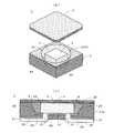
本発明の第1の実施形態に係る発光装置について、図1(a)(b)を参照して説明する。本実施形態の発光装置1は、実装基板2上に実装された発光素子3と、この発光素子3から出射する光の波長を変換する蛍光体を含有する光変換部材4と、を備える。発光素子3の近傍には、放熱性及び絶縁性を有する金属又は金属粉を含有する樹脂から形成される絶縁性放熱部材5が配置される。また、放熱性を有する金属又は金属粉を含有する樹脂から形成される金属含有放熱部材6が、絶縁性放熱部材5の外周と接するように配置される。 A light emitting device according to a first embodiment of the present invention will be described with reference to FIGS. The
絶縁性放熱部材5は、発光素子3の側面に接していることが望ましい。また、絶縁性放熱部材5及び金属含有放熱部材6は、いずれか一方が光変換部材4と接していればよいが、それらの上面が同一平面となるように形成され、絶縁性放熱部材5及び金属含有放熱部材6の両方が光変換部材4と接していることが望ましい。なお、光変換部材4は、絶縁性放熱部材5及び金属含有放熱部材6だけでなく、発光素子3とも接するように配置されることが望ましい。 The insulating
実装基板2は、電気絶縁性を有し、且つ熱伝導率の高い基板であり、例えば、酸化アルミニウム(Al2O3)や窒化アルミニウム(AlN)等の金属酸化物(セラミックスを含む)、金属窒化物、又は金属、樹脂等の材料から構成される。実装基板2の一表面には、金(Au)又は銀(Ag)等の導電性金属から成る配線パターン21が設けられ、この配線パターン21が発光素子3と電気的に接続される。配線パターン21の一端側には、Au、半田等の金属材料から成るバンプ(不図示)を介して接合される素子端子部(不図示)が形成され、他端側に外部接続用端子部21aが形成される(図1(a)参照)。なお、図1(b)は配線パターン21の図示を省略している。配線パターン21は、素子端子部及び外部接続用端子部21aを除き、絶縁層によって覆われている。外部接続用端子部21aは、発光装置1の平面視において、絶縁性放熱部材5及び金属含有放熱部材6よりも外側の実装基板2上に配置される。なお、実装基板2中にビアホールを形成し、このビアホールに導電性金属等から成る配線を挿通させることにより、実装基板2表面ではなく、実装基板2裏面に配線パターン21を設けてもよい(不図示)。The
発光素子3は、光変換部材4へ光を出射することにより、発光装置1として所望の光色の発光を可能とする光源であれば特に限定されないが、好ましくは、青色光を放射するGaN系青色LEDチップが用いられる。本実施形態においては、発光素子3として矩形板状のチップを示すが、発光素子3の形状はこれに限られず、発光装置1の用途等に応じたものが用いられる。発光素子3は、具体構成として、p形窒化物半導体層、発光層及びn形窒化物半導体層の積層構造から成る発光部と、n形窒化物半導体層に電気的に接続されたカソード電極と、p形窒化物半導体層に電気的に接続されたアノード電極とを備える。カソード電極及びアノード電極は、素子の下面側に形成され、これらカソード電極及びアノード電極がバンプを介して配線パターン21の素子端子部に接合されることにより、発光素子3は実装基板2に実装される。なお、ここでは、発光素子3の実装方法として、フェイスダウン式の発光素子3をフリップチップ実装する例を示したが、発光素子3はフェイスアップ式のチップであってもよく、この場合、例えば、ダイスボンドとワイヤを用いて接続する方法等が用いられる。 The
光変換部材4は、シリコーン樹脂、エポキシ樹脂又はアクリル樹脂等の透光性を有する樹脂材料に蛍光体を混練させ、この蛍光体含有樹脂材料をシート状に形成された部材であり、発光素子3上に配置される。また、光変換部材4は、発光素子3上に上記樹脂材料を、例えば、印刷、インクジェット、ボッティング等の塗布方法により塗布することによって形成されてもよい。なお、樹脂材料には、熱伝導率を上げるために、フィラーを含有させてもよい。 The
蛍光体には、発光装置1に求められる演色性等の発光性能、及び発光素子3の発光波長等の発光特性に応じた種類のものが用いられ、所定の含有濃度となるよう樹脂材料に混練される。例えば、発光素子3がGaN系青色LEDチップである場合、黄色蛍光体として汎用されるYAG系蛍光体が樹脂材料に混練され、所定形状の光変換部材4が作成される。なお、光変換部材4は、蛍光体の含有濃度を、例えば、発光素子3の近傍側ほど漸次濃くなるように形成されてもよい。また、蛍光体の含有濃度が異なる複数の樹脂層を積層させてもよい。更に、絶縁性放熱部材5の近傍の蛍光体の含有濃度が濃くなるようにしてもよく、こうすれば、波長変換時に生じる熱を効率的に絶縁性放熱部材5に伝達することができる。 As the fluorescent material, a fluorescent material of a kind corresponding to light emitting performance such as color rendering required for the
絶縁性放熱部材5は、例えば、酸化アルミニウム(Al2O3)、窒化アルミニウム(AlN)又は酸化チタン(TiO2)等の絶縁性を有する金属酸化物又は金属窒化物等の粒状材料を、シリコーン樹脂、エポキシ樹脂等の樹脂材料に含有させて作成される。なお、樹脂に含有される粒状材料又は粉状材料は、光反射性の高い材料が好ましい。こうすれば、発光素子3から出射された光を光変換部材4側へ反射することができるので、絶縁性放熱部材5に吸収又は拡散等して損失する光が少なくなり、光利用効率が向上する。The insulating
絶縁性放熱部材5は、予め発光素子3を実装基板2上に実装すると共に、発光素子3との間に隙間をあけて金属含有放熱部材6を配置しておき、発光素子3と金属含有放熱部材6との隙間に、上述の樹脂材料をポッティングすることにより配置される。また、金属酸化物等を含有させた樹脂材料から成るペーストを、スクリーン印刷を用いて塗布することにより、絶縁性放熱部材5を発光素子3上に配置してもよい。更に、絶縁性放熱部材5の形状を、その内周側面が発光素子3の外周側面に適合するように形成しておき、形成された絶縁性放熱部材5を発光素子3の外周に嵌め込んでもよい。 The insulating
金属含有放熱部材6は、例えば、アルミニウム(Al)や銀(Ag)等の金属又はAlやAgの金属粒子を、シリコーン樹脂、エポキシ樹脂又はアクリル樹脂等の樹脂材料に含有させて作成される。金属含有放熱部材6は、その内周面と発光素子3との間に隙間ができる形状となるように形成され、実装基板2上に配置される。また、予め発光素子3の外周側面に適合するように形成された絶縁性放熱部材5を実装基板2上に配置し、絶縁性放熱部材5の外周に、スクリーン印刷を用いてペースト状の金属粒子が混入された樹脂を塗布してもよい。 The metal-containing
この発光装置1においては、発光素子3から出射する光の波長が、蛍光体を含有する光変換部材4によって変換され、波長を変換された光が光変換部材4から出射される。このとき、光変換部材4に含まれる蛍光体は、励起されて発熱する。この熱は、光変換部材4と接する絶縁性放熱部材5又は金属含有放熱部材6に伝達される。また、絶縁性放熱部材5又は金属含有放熱部材6のうちの一方の放熱部材に伝達された熱は、他方の放熱部材に熱を伝達され、それらの熱は実装基板2へ伝達される。 In the
ここで、光変換部材4が、絶縁性放熱部材5及び金属含有放熱部材6の両方並びに発光素子3に接する構成における熱の伝達経路について説明する。光変換部材4のうち、発光素子3の発光面に面する箇所は、蛍光体の励起に伴い、最も温度が高くなる。この箇所で発生した熱は、発光素子3に伝達され、更に、発光素子3から実装基板2に伝達される。また、発光素子3の発光面に面する箇所で発生した熱は、光変換部材4の外側へ放射状に広がると共に、絶縁性放熱部材5に伝達され、この熱は、直接的に実装基板2に、又は絶縁性放熱部材5の外周と接する金属含有放熱部材6を介して実装基板2に伝達される。また、光変換部材4から金属含有放熱部材6に伝達された熱は、直接的に実装基板2に、又は絶縁性放熱部材5を介して実装基板2に伝達される。金属含有放熱部材6に伝達された熱は、空気中へも放熱される。 Here, the heat transfer path in the configuration in which the
このように、絶縁性放熱部材5及び金属含有放熱部材6の2種類の放熱部材を備えたことにより、光変換部材4で発生した熱が、複数の伝達経路を介して伝達されるので、光変換部材4の熱が効率的に放熱される。従って、本実施形態の発光装置1によれば、光変換部材4に含まれる蛍光体の熱を、簡易な構成で、効率的に放熱することができ、光変換部材4の温度上昇を防ぐと共に、蛍光体の発光効率の低下を抑制することができる。 As described above, by providing two types of heat radiating members, the insulating
また、発光素子3の近傍に絶縁性放熱部材5が配置されているので、金属含有放熱部材6と発光素子3との間の絶縁性を確保することができる。更に、発光素子3と金属含有放熱部材6との間に、樹脂材料から成る絶縁性放熱部材5が配置され、この絶縁性放熱部材5が緩衝材として機能するので、発光装置1の寸法安定性を向上させることができる。また、金属含有放熱部材6に、AlやAgのような光反射率の高い金属材料を用いることにより、絶縁性放熱部材5を透過して金属含有放熱部材6に入射した光を光変換部材4側へ反射することができるので、光利用効率を向上させることができる。 Moreover, since the insulating
また、金属含有放熱部材6の熱伝導性が、絶縁性放熱部材5の熱伝導性よりも高くなるように、絶縁性放熱部材5及び金属含有放熱部材6に含有される金属材料等の種類及び濃度、樹脂の組成等が調整されていてもよい。こうすれば、光変換部材4の熱がより効率的に絶縁性放熱部材5から金属含有放熱部材6へ伝達されるので、放熱性能を向上させることができる。また、発光素子3の近傍に配置される絶縁性放熱部材5の温度上昇を抑制できるので、発光素子3で発生した熱も効率的に放熱することができる。更に、発光装置1の正面視における金属含有放熱部材6及び光変換部材4の形状が、略同形状となるよう、それらが形成されることが望ましい。こうすれば、金属含有放熱部材6上に光変換部材4を配置して固定することにより、発光装置1のパッケージングが容易となる。 Further, the types of metal materials and the like contained in the insulating
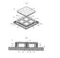
次に、本実施形態の第2の実施形態に係る発光装置について、図2(a)(b)を参照して説明する。本実施形態に係る発光装置1は、発光素子3が、実装基板2に形成された凹部22に実装され、発光素子3と凹部22との間に絶縁性放熱部材5が配置されているものである。本実施形態においては、凹部22が形成された実装基板2が、上記第1の実施形態における金属含有放熱部材6として機能する。 Next, a light emitting device according to a second embodiment of the present embodiment will be described with reference to FIGS. In the
本実施形態の実装基板2は、発光素子3の厚みを収容できる凹部22、発光素子3が実装される実装面23及び配線パターン21の形成することができるだけの厚みを有する。凹部22は、光出射方向に形成される開口部24が広く、実装面23へ向けて狭くなるように形成されたテーパ状の傾斜面25を有する。また、凹部22は、実装面23上に発光素子3を実装したときの発光素子3の上面の高さと、実装基板2の上面の高さとがほぼ等しくなるように形成される。これにより、発光素子3と凹部22との間に絶縁性放熱部材5が配置(充填)され、発光素子3上に光変換部材4が配置されたときに、発光素子3、絶縁性放熱部材5及び実装基板2の上面が光変換部材4と接する。 The mounting
また、本実施形態においては、凹部22が形成された基板2を、金属含有放熱部材6として機能させるため、実装基板2には金属製又は金属を分散した絶縁材料から成る基板が用いられ、発光素子3の実装面23には絶縁層26が設けられる。なお、非金属製の基板を用いる場合、この基板に上述した凹部22と略同形状の凹部を形成し、この凹部に金属材料から成る碗状部材を嵌め込む、又は非金属製の基板に形成された凹部に金属材料をコーティングすることにより、これらを金属含有放熱部材6として機能させてもよい。また、金属材料として、AlやAgのような光反射率の高い材料を用いることにより、凹部22の発光素子3からの光が入射する面が、光反射性を有するように構成することができる。こうすれば、凹部22の傾斜面25が、絶縁性放熱部材5を透過して傾斜面25に入射した光を光変換部材4側へ反射する反射部材として機能するので、光利用効率を向上させることができる。 Further, in the present embodiment, in order to cause the
実装面23には、発光素子3のカソード電極及びアノード電極に対応する位置に、ビアホール27が形成され、また、実装基板2の裏面側に配線パターン21を敷くための配線路28が形成される(図2(b)参照)。これらビアホール27及び配線路28には、実装面23と同様に、絶縁層26が被覆され、絶縁層26で被覆されたビアホール27及び配線路28に配線パターン21が施される。このように、配線パターン21を立体的に設けることにより、発光装置1の小型化を実現することができる。 A via
このように、金属製の実装基板2を加工して凹部22を形成する、又は非金属製の実装基板2に形成された凹部22を金属材料で加工することにより、実質的に金属含有放熱部材6を容易に形成することができる。また、発光素子3と凹部22との間に樹脂材料を充填することにより、絶縁性放熱部材5を容易に形成することができる。更に、凹部22を形成した実装基板2上に光変換部材4を配置して固定することにより、発光装置1のパッケージングも容易となる。従って、本実施形態の発光装置1によれば、蛍光体の発光効率の低下を抑制することができるだけでなく、発光装置1の製造効率を向上させることができると共に、製造コストを低減することができる。 In this way, the
次に、本実施形態の第3の実施形態に係る発光装置について、図3(a)(b)を参照して説明する。本実施形態に係る発光装置1は、発光素子3が、その複数個が基板上に実装されているものである。また、各発光素子3の側面には、個別に絶縁性放熱部材5が配置され、夫々の絶縁性放熱部材5の外周をカバーするように、金属含有放熱部材6が配置されている。なお、図例では、4個の発光素子3が実装されている構成を示しているが、発光素子3の個数は、発光装置1のパッケージサイズ及び所用出力等に応じて適宜に選択される。また、配線パターン21も、発光素子3の個数、及び実装位置に応じた適宜のパターンに形成される。 Next, a light emitting device according to a third embodiment of the present embodiment will be described with reference to FIGS. In the
光変換部材4は、図示したように、金属含有放熱部材6に対応する一部材であってもよいし、各発光素子3に対応する複数の部材であってもよい。なお、光変換部材4を一部材とすれば、複数の発光素子3から出射された光が、光変換部材4内で混光されるので、光変換部材4の出射面から面一な発光が可能となる。 As illustrated, the
本実施形態の発光装置1によれば、複数個の発光素子3を実装させることにより、発光装置1の用途等に応じた高出力化が可能になる。また、光変換部材4の蛍光体が高出力の光に曝されても、各発光素子3の側面に配置された絶縁性放熱部材5及び金属含有放熱部材6によって効率的に放熱されるので、光変換部材4の温度上昇を防ぐと共に、蛍光体の発光効率の低下を抑制することができる。 According to the
なお、本発明は、上記実施形態に限らず、種々の変形が可能である。例えば、実装基板2に複数の凹部22を形成し、各凹部22に発光素子3を実装する共に、夫々の凹部22と発光素子3との間に、絶縁性放熱部材5を配置してもよい。 In addition, this invention is not restricted to the said embodiment, A various deformation | transformation is possible. For example, a plurality of
1 発光素子
2 実装基板(基板)
22 凹部
3 発光素子
4 光変換部材
5 絶縁性放熱部材
6 金属含有放熱部材1 Light-Emitting
22 recessed
Claims (5)
Translated fromJapanese前記発光素子の近傍に配置され、放熱性及び絶縁性を有する金属又は金属粉を含有する樹脂から形成される絶縁性放熱部材と、
前記絶縁性放熱部材と接し、放熱性を有する金属又は金属粉を含有する樹脂から形成される金属含有放熱部材と、を有し、
前記絶縁性放熱部材及び金属含有放熱部材の両方が前記光変換部材及び前記基板と接していることを特徴とする発光装置。A light emitting devicecomprising: a light emitting element; a substrate on which the light emitting element is mounted ; and a light conversion member containing a phosphor that converts a wavelength of light emitted from the light emitting element.
An insulating heat dissipating member which is disposed in the vicinity of the light emitting element and is formed from a resin containing metal or metal powder having heat dissipation and insulation;
A metal-containing heat dissipation member formed from a resin containing metal or metal powder having heat dissipation properties in contact with the insulating heat dissipation member;
Both the insulating heat radiating member and the metal-containing heat radiating memberare in contact with the light conversion memberand the substrate .
Priority Applications (1)
| Application Number | Priority Date | Filing Date | Title |
|---|---|---|---|
| JP2010144369AJP5662064B2 (en) | 2010-06-25 | 2010-06-25 | Light emitting device |
Applications Claiming Priority (1)
| Application Number | Priority Date | Filing Date | Title |
|---|---|---|---|
| JP2010144369AJP5662064B2 (en) | 2010-06-25 | 2010-06-25 | Light emitting device |
Publications (2)
| Publication Number | Publication Date |
|---|---|
| JP2012009633A JP2012009633A (en) | 2012-01-12 |
| JP5662064B2true JP5662064B2 (en) | 2015-01-28 |
Family
ID=45539852
Family Applications (1)
| Application Number | Title | Priority Date | Filing Date |
|---|---|---|---|
| JP2010144369AActiveJP5662064B2 (en) | 2010-06-25 | 2010-06-25 | Light emitting device |
Country Status (1)
| Country | Link |
|---|---|
| JP (1) | JP5662064B2 (en) |
Cited By (1)
| Publication number | Priority date | Publication date | Assignee | Title |
|---|---|---|---|---|
| KR20200018867A (en)* | 2018-08-13 | 2020-02-21 | 주식회사 루멘스 | Light emitting diode package and manufacturing method thereof |
Families Citing this family (9)
| Publication number | Priority date | Publication date | Assignee | Title |
|---|---|---|---|---|
| WO2013175706A1 (en)* | 2012-05-25 | 2013-11-28 | 日本電気株式会社 | Optical element, light-emitting device, and projection device |
| JP2014041993A (en)* | 2012-07-24 | 2014-03-06 | Toyoda Gosei Co Ltd | Light-emitting device and method of manufacturing the same |
| WO2014080705A1 (en)* | 2012-11-22 | 2014-05-30 | シャープ株式会社 | Light emitting apparatus, method for manufacturing same, lighting apparatus, and headlamp |
| JP2015092524A (en)* | 2013-11-08 | 2015-05-14 | 日立金属株式会社 | Heat radiation structure of electronic component |
| JP6847661B2 (en)* | 2014-01-08 | 2021-03-24 | ルミレッズ ホールディング ベーフェー | Luminescent device and its formation method |
| WO2016093325A1 (en)* | 2014-12-11 | 2016-06-16 | シチズン電子株式会社 | Light emitting device |
| JP6908859B2 (en)* | 2014-12-25 | 2021-07-28 | 日亜化学工業株式会社 | Semiconductor devices and methods for manufacturing semiconductor devices |
| US20230033309A1 (en)* | 2020-02-21 | 2023-02-02 | Panasonic Holdings Corporation | Semiconductor laser device |
| JP7502636B2 (en)* | 2020-09-29 | 2024-06-19 | 日亜化学工業株式会社 | Light emitting device manufacturing method and light emitting device |
Family Cites Families (5)
| Publication number | Priority date | Publication date | Assignee | Title |
|---|---|---|---|---|
| TWI257184B (en)* | 2004-03-24 | 2006-06-21 | Toshiba Lighting & Technology | Lighting apparatus |
| JP4516337B2 (en)* | 2004-03-25 | 2010-08-04 | シチズン電子株式会社 | Semiconductor light emitting device |
| WO2006101174A1 (en)* | 2005-03-24 | 2006-09-28 | Kyocera Corporation | Light emitting element storing package, light emitting device and lighting apparatus |
| JP2007294867A (en)* | 2006-03-28 | 2007-11-08 | Toshiba Lighting & Technology Corp | Light emitting device |
| JP5224173B2 (en)* | 2008-03-07 | 2013-07-03 | スタンレー電気株式会社 | Semiconductor light emitting device |
- 2010
- 2010-06-25JPJP2010144369Apatent/JP5662064B2/enactiveActive
Cited By (2)
| Publication number | Priority date | Publication date | Assignee | Title |
|---|---|---|---|---|
| KR20200018867A (en)* | 2018-08-13 | 2020-02-21 | 주식회사 루멘스 | Light emitting diode package and manufacturing method thereof |
| KR102561705B1 (en)* | 2018-08-13 | 2023-08-01 | 주식회사 루멘스 | Light emitting diode package and manufacturing method thereof |
Also Published As
| Publication number | Publication date |
|---|---|
| JP2012009633A (en) | 2012-01-12 |
Similar Documents
| Publication | Publication Date | Title |
|---|---|---|
| JP5662064B2 (en) | Light emitting device | |
| JP5437177B2 (en) | Light emitting device | |
| US8203218B2 (en) | Semiconductor device package including a paste member | |
| US11189601B2 (en) | Reflective solder mask layer for LED phosphor package | |
| JP4881358B2 (en) | Light emitting device | |
| US20090072250A1 (en) | Chip type semiconductor light emitting device | |
| US8502251B2 (en) | LED module comprising a dome-shaped color conversion layer | |
| JP4678391B2 (en) | Lighting equipment | |
| US9293663B1 (en) | Light-emitting unit and semiconductor light-emitting device | |
| JP2004327863A (en) | Semiconductor light emitting device provided with a reflector having heat dissipation function | |
| EP2461380A2 (en) | Light emitting device package and manufacturing method thereof | |
| JP6583764B2 (en) | Light emitting device and lighting device | |
| JP2005093681A (en) | Light-emitting device | |
| JP2014140014A (en) | Light emitting device and manufacturing method of the same | |
| TW201218428A (en) | Light emitting diode package structure | |
| JP2009267039A (en) | Light-emitting device | |
| JP4773755B2 (en) | Chip-type semiconductor light emitting device | |
| JP2005209958A (en) | Light emitting element storage package and light emitting device | |
| JP2007243056A (en) | Light emitting device | |
| JP2008251664A (en) | Lighting device | |
| JP2008244421A (en) | Light emitting device and manufacturing method thereof | |
| JP2009071090A (en) | Light emitting device | |
| KR20140004351A (en) | Light emitting diode package | |
| JP5924947B2 (en) | Light emitting device | |
| JP2007116107A (en) | Light emitting device |
Legal Events
| Date | Code | Title | Description |
|---|---|---|---|
| A711 | Notification of change in applicant | Free format text:JAPANESE INTERMEDIATE CODE: A712 Effective date:20120117 | |
| A621 | Written request for application examination | Free format text:JAPANESE INTERMEDIATE CODE: A621 Effective date:20130513 | |
| A131 | Notification of reasons for refusal | Free format text:JAPANESE INTERMEDIATE CODE: A131 Effective date:20140527 | |
| A521 | Written amendment | Free format text:JAPANESE INTERMEDIATE CODE: A523 Effective date:20140718 | |
| A711 | Notification of change in applicant | Free format text:JAPANESE INTERMEDIATE CODE: A711 Effective date:20141007 | |
| RD03 | Notification of appointment of power of attorney | Free format text:JAPANESE INTERMEDIATE CODE: A7423 Effective date:20141023 | |
| TRDD | Decision of grant or rejection written | ||
| A01 | Written decision to grant a patent or to grant a registration (utility model) | Free format text:JAPANESE INTERMEDIATE CODE: A01 Effective date:20141202 | |
| A61 | First payment of annual fees (during grant procedure) | Free format text:JAPANESE INTERMEDIATE CODE: A61 Effective date:20141204 | |
| R150 | Certificate of patent (=grant) or registration of utility model | Ref document number:5662064 Country of ref document:JP Free format text:JAPANESE INTERMEDIATE CODE: R150 |