JP5659906B2 - Inverter circuit and display device - Google Patents
Inverter circuit and display deviceDownload PDFInfo
- Publication number
- JP5659906B2 JP5659906B2JP2011073022AJP2011073022AJP5659906B2JP 5659906 B2JP5659906 B2JP 5659906B2JP 2011073022 AJP2011073022 AJP 2011073022AJP 2011073022 AJP2011073022 AJP 2011073022AJP 5659906 B2JP5659906 B2JP 5659906B2
- Authority
- JP
- Japan
- Prior art keywords
- transistor
- voltage
- gate
- voltage line
- terminal
- Prior art date
- Legal status (The legal status is an assumption and is not a legal conclusion. Google has not performed a legal analysis and makes no representation as to the accuracy of the status listed.)
- Active
Links
Images


Landscapes
- Electroluminescent Light Sources (AREA)
- Control Of Indicators Other Than Cathode Ray Tubes (AREA)
- Control Of El Displays (AREA)
- Logic Circuits (AREA)
Description
Translated fromJapanese本発明は、例えば有機EL(Electro Luminescence)素子を用いた表示装置に好適に適用可能なインバータ回路に関する。また、本発明は、上記インバータ回路を備えた表示装置に関する。 The present invention relates to an inverter circuit that can be suitably applied to a display device using, for example, an organic EL (Electro Luminescence) element. Moreover, this invention relates to the display apparatus provided with the said inverter circuit.
近年、画像表示を行う表示装置の分野では、画素の発光素子として、流れる電流値に応じて発光輝度が変化する電流駆動型の光学素子、例えば有機EL素子を用いた表示装置が開発され、商品化が進められている。有機EL素子は、液晶素子などと異なり自発光素子である。そのため、有機EL素子を用いた表示装置(有機EL表示装置)では、有機EL素子に流れる電流値を制御することで、発色の階調が得られる。 In recent years, in the field of display devices that perform image display, display devices using current-driven optical elements, such as organic EL elements, whose light emission luminance changes according to the value of a flowing current have been developed as light-emitting elements of pixels. Is being promoted. Unlike a liquid crystal element or the like, the organic EL element is a self-luminous element. Therefore, in a display device (organic EL display device) using an organic EL element, a gradation of color can be obtained by controlling a current value flowing through the organic EL element.
有機EL表示装置では、液晶表示装置と同様、その駆動方式として単純(パッシブ)マトリクス方式とアクティブマトリクス方式とがある。前者は、構造が単純であるものの、大型かつ高精細の表示装置の実現が難しいなどの問題がある。そのため、現在では、アクティブマトリクス方式の開発が盛んに行なわれている。この方式は、画素ごとに配した発光素子に流れる電流を駆動トランジスタによって制御するものである。 In the organic EL display device, similarly to the liquid crystal display device, there are a simple (passive) matrix method and an active matrix method as its driving method. Although the former has a simple structure, there is a problem that it is difficult to realize a large-sized and high-definition display device. For this reason, active matrix systems are currently being actively developed. In this method, a current flowing through a light emitting element arranged for each pixel is controlled by a driving transistor.
上記の駆動トランジスタでは、閾値電圧Vthや移動度μが経時的に変化したり、製造プロセスのばらつきによって閾値電圧Vthや移動度μが画素ごとに異なったりする場合がある。閾値電圧Vthや移動度μが画素ごとに異なる場合には、駆動トランジスタに流れる電流値が画素ごとにばらつくので、駆動トランジスタのゲートに同じ電圧を印加しても、有機EL素子の発光輝度がばらつき、画面の一様性(ユニフォーミティ)が損なわれる。そこで、閾値電圧Vthや移動度μの変動に対する補正機能を組み込んだ表示装置が開発されている(例えば、特許文献1参照)。In the drive transistor described above, the threshold voltage Vth and the mobility μ may change over time, or the threshold voltage Vth and the mobility μ may vary from pixel to pixel due to manufacturing process variations. When the threshold voltage Vth and the mobility μ are different for each pixel, the value of the current flowing through the driving transistor varies from pixel to pixel. Therefore, even if the same voltage is applied to the gate of the driving transistor, the light emission luminance of the organic EL element is Variations and screen uniformity are lost. In view of this, a display device incorporating a correction function for variations in threshold voltage Vth and mobility μ has been developed (see, for example, Patent Document 1).
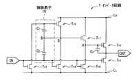
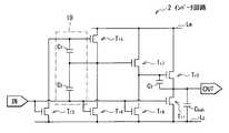
閾値電圧Vthや移動度μの変動に対する補正は、画素ごとに配した画素回路によって行われる。この画素回路は、例えば、図32に示したように、有機EL素子111に流れる電流を制御する駆動トランジスタTr100と、信号線DTLの電圧を駆動トランジスタTr100に書き込む書き込みトランジスタTr200と、保持容量Csとによって構成されており、2Tr1Cの回路構成となっている。駆動トランジスタTr100および書き込みトランジスタTr200は、例えば、nチャネルMOS型の薄膜トランジスタ(TFT(Thin Film Transistor))により形成されている。Correction for variations in threshold voltage Vth and mobility μ is performed by a pixel circuit arranged for each pixel. For example, as shown in FIG. 32, the pixel circuit includes a drive transistor Tr100 that controls a current flowing in the
図31は、画素回路に印加される電圧波形の一例と、駆動トランジスタTr100のゲート電圧Vgおよびソース電圧Vsの変化の一例とを表したものである。図31(A)には信号線DTLに、信号電圧Vsigと、オフセット電圧Vofsが印加されている様子が示されている。図31(B)には書込線WSLに、書き込みトランジスタTr200をオンする電圧Vddと、書き込みトランジスタTr200をオフする電圧Vssが印加されている様子が示されている。図31(C)には電源線PSLに、ハイ電圧VccHと、ロー電圧VccLが印加されている様子が示されている。さらに、図31(D),(E)には、電源線PSL、信号線DTLおよび書込線WSLへの電圧印加に応じて、駆動トランジスタTr100のゲート電圧Vgおよびソース電圧Vsが時々刻々変化している様子が示されている。FIG. 31 shows an example of a voltage waveform applied to the pixel circuit and an example of changes in the gate voltage Vg and the source voltage Vs of the drive transistor Tr100 . FIG.31A shows a state in which the signal voltage Vsig and the offset voltage Vofs are applied to the signal line DTL. The write line WSL in FIG 31 (B), and the voltage Vdd for turning on the writing transistor Tr200, the voltage Vss is shown to have been applied to turn off the write transistor Tr200. FIG.31C shows a state in which the high voltage VccH and the low voltage VccL are applied to the power supply line PSL. Further, in FIGS. 31D and 31E, the gate voltage Vg and the source voltage Vs of the drive transistor Tr100 are sometimes changed depending on the voltage application to the power supply line PSL, the signal line DTL, and the write line WSL. It shows how it changes every moment.
図31から、1H内に2回、WSパルスPが書込線WSLに印加されており、1回目のWSパルスPによって閾値補正が行われ、2回目のWSパルスPによって移動度補正と信号書き込みが行われていることがわかる。つまり、図31において、WSパルスPは、信号書込みだけでなく、駆動トランジスタTr100の閾値補正や移動度補正にも用いられている。From FIG. 31, the WS pulse P is applied to the write line WSL twice within 1H, threshold correction is performed by the first WS pulse P, and mobility correction and signal writing are performed by the second WS pulse P. Can be seen. That is, in FIG. 31, WS pulse P not only signal writing is also used in the threshold correction and the mobility correction of the driving transistor Tr100.
ところで、アクティブマトリクス方式の表示装置では、信号線DTLを駆動する水平駆動回路(図示せず)や、各画素113を順次選択する書き込み走査回路(図示せず)は、いずれも基本的にシフトレジスタ(図示せず)を含んで構成されており、画素113の各列または各行に対応して、1段ごとにバッファ回路(図示せず)を備えている。例えば、書き込み走査回路内のバッファ回路は、典型的には、2つのインバータ回路を直列に接続して構成されている。ここで、インバータ回路は、例えば、図33に示したように、2つのnチャネルMOS型のトランジスタTr1,Tr2が直列接続された単チャネル型の回路構成となっている。図33に記載のインバータ回路200は、ハイレベルの電圧が印加される高電圧配線LHと、ローレベルの電圧が印加される低電圧配線LLとの間に挿入されている。高電圧配線LH側のトランジスタTr2のゲートが高電圧配線LHに接続されており、低電圧配線LL側のトランジスタTr1のゲートが入力端子INに接続されている。さらに、トランジスタTr1とトランジスタTr2との接続点Cが出力端子OUTに接続されている。Incidentally, in an active matrix display device, a horizontal driving circuit (not shown) for driving the signal line DTL and a writing scanning circuit (not shown) for sequentially selecting each
インバータ回路200では、例えば、図34に示したように、入力端子INの電圧VinがVssとなっている時、出力端子OUTの電圧VoutがVddとはならず、Vdd−Vth2となってしまう。つまり、出力端子OUTの電圧Voutには、トランジスタTr2の閾値電圧Vth2が含まれており、出力端子OUTの電圧Voutは、トランジスタTr2の閾値電圧Vth2のばらつきの影響を大きく受けてしまう。In the inverter circuit 200, for example, as shown in FIG. 34, when the voltage Vin of the input terminal IN is Vss , the voltage Vout of the output terminal OUT does not become Vdd , but Vdd −V It becomesth2 . In other words, the voltage Vout of the output terminal OUT, and includes a threshold voltage Vth2 of the transistor Tr2, the voltage Vout of the output terminal OUT, greatly affected by variations in the threshold voltage Vth2 of the transistor Tr2 End up.
そこで、例えば、図35のインバータ回路300に示したように、トランジスタTr2のゲートとドレインとを互いに電気的に分離し、ドレインの電圧Vddよりも高い電圧Vdd2(≧Vdd+Vth)が印加される高電圧配線LH2にゲートを接続することが考えられる。また、例えば、図36のインバータ回路400に示したようなブートストラップ型の回路構成が考えられる。具体的には、トランジスタTr2のゲートと高電圧配線LHとの間にトランジスタTr12を挿入し、トランジスタTr12のゲートを高電圧配線LHに接続するとともに、トランジスタTr2のゲートとトランジスタTr12のソースとの接続点Dと、接続点Cとの間に容量素子C10を挿入した回路構成が考えられる。Therefore, for example, as shown in the inverter circuit 300 of FIG. 35, the gate and drain of the transistor Tr2 are electrically separated from each other, and the voltage Vdd2 (≧ Vdd + Vth ) higher than the drain voltage Vdd. It is conceivable to connect the gate to the high voltage wiring LH2 to which is applied. Further, for example, a bootstrap type circuit configuration as shown in the inverter circuit 400 of FIG. 36 is conceivable. Specifically, the transistor Tr12 is inserted between the gate of the transistor Tr2 and the high voltage wiring LH , the gate of the transistor Tr12 is connected to the high voltage wiring LH , and the gate of the transistor Tr2 and the transistor A circuit configuration in which a capacitive element C10 is inserted between the connection point D with the source of Tr12 and the connection point C is conceivable.
しかし、図33、図35、図36のいずれの回路においても、入力電圧Vinがハイとなっている時、つまり、出力電圧Voutがローとなっている時まで、トランジスタTr1,Tr2を介して、高電圧配線LH側から低電圧配線LL側に向かって電流(貫通電流)が流れてしまう。その結果、インバータ回路での消費電力も大きくなってしまう。また、図33、図35、図36の回路においては、例えば、図34(B)の破線で囲んだ箇所に示したように、入力電圧VinがVddとなっている時、出力電圧VoutがVssとはならず、出力電圧Voutの波高値がばらついてしまう。その結果、画素回路112内の駆動トランジスタTr100の閾値補正や移動度補正が画素回路112ごとにばらついてしまい、そのばらつきが輝度のばらつきとなってしまうという問題があった。However, Figure 33, Figure 35, in any of the circuit of Figure 36, when the input voltage Vin is high, that is, until the output voltage Vout is in the low, transistors Tr1, Tr2 As a result, a current (through current) flows from the high voltage wiring LH side toward the low voltage wiring LL side. As a result, power consumption in the inverter circuit also increases. In the circuits of FIGS. 33, 35, and 36, for example, when the input voltage Vin is Vdd as shown in the portion surrounded by the broken line in FIG. 34B, the output voltage Vout does not become Vss, and the peak value of the output voltage Vout varies. As a result, there has been a problem that threshold correction and mobility correction of the drive transistor Tr100 in the
なお、上述の問題は、表示装置の走査回路に限って生じるものではなく、他のデバイスにおいても同様に生じ得るものである。 Note that the above-described problem does not occur only in the scanning circuit of the display device, and may occur in other devices as well.
本発明はかかる問題点に鑑みてなされたものであり、その目的は、消費電力を抑えつつ、出力電圧の波高値を所望の値にすることの可能なインバータ回路、およびこのインバータ回路を備えた表示装置を提供することにある。 The present invention has been made in view of such problems, and an object thereof is to provide an inverter circuit capable of setting a peak value of an output voltage to a desired value while suppressing power consumption, and the inverter circuit. It is to provide a display device.
本発明の第1のインバータ回路は、互いに同一チャネル型の第1トランジスタ、第2トランジスタ、第3トランジスタ、第4トランジスタ、第5トランジスタ、第6トランジスタおよび第7トランジスタを備えたものである。このインバータ回路は、さらに、第1容量素子、第2容量素子および第3容量素子と、入力端子および出力端子とを備えている。ここで、第1トランジスタは、入力端子の電圧(入力電圧)と第1電圧線の電圧との電位差またはそれに対応する電位差に応じて出力端子と第1電圧線との電気的な接続を継断するようになっている。第2トランジスタは、当該第2トランジスタのゲート電圧と、出力端子の電圧との電位差またはそれに対応する電位差に応じて第2電圧線と出力端子との電気的な接続を継断するようになっている。第3トランジスタは、入力端子の電圧と第3電圧線の電圧との電位差またはそれに対応する電位差に応じて第5トランジスタのゲートと第3電圧線との電気的な接続を継断するようになっている。第4トランジスタは、入力端子の電圧と第4電圧線の電圧との電位差またはそれに対応する電位差に応じて第5トランジスタのソースまたはドレインである第1端子と第4電圧線との電気的な接続を継断するようになっている。第1容量素子および第2容量素子は、入力端子と第5トランジスタのゲートとの間に直列に挿入されており、第1容量素子と第2容量素子との電気的な接続点が、第1端子に電気的に接続されている。第3容量素子は、第2トランジスタのゲートと出力端子との間に挿入されている。第5トランジスタは、第1容量素子の端子間電圧またはそれに対応する電圧に応じて第5電圧線と第1端子との電気的な接続を継断するようになっている。第6トランジスタは、入力端子の電圧と第6電圧線の電圧との電位差またはそれに対応する電位差に応じて第2トランジスタのゲートと第6電圧線との電気的な接続を継断するようになっている。第7トランジスタは、第1端子の電圧と第2トランジスタのゲート電圧との電位差またはそれに対応する電位差に応じて第7電圧線と第2トランジスタのゲートとの電気的な接続を継断するようになっている。 The first inverter circuit of the present invention includes a first transistor, a second transistor, a third transistor, a fourth transistor, a fifth transistor, a sixth transistor, and a seventh transistor that are of the same channel type. The inverter circuit further includes a first capacitive element, a second capacitive element, a third capacitive element, an input terminal, and an output terminal. Here, the first transistor cuts off the electrical connection between the output terminal and the first voltage line according to the potential difference between the voltage of the input terminal (input voltage) and the voltage of the first voltage line or the corresponding potential difference. It is supposed to be. The second transistor cuts off the electrical connection between the second voltage line and the output terminal according to the potential difference between the gate voltage of the second transistor and the voltage at the output terminal or the corresponding potential difference. Yes. The third transistor cuts off the electrical connection between the gate of the fifth transistor and the third voltage line according to the potential difference between the voltage of the input terminal and the voltage of the third voltage line or the corresponding potential difference. ing. The fourth transistor electrically connects the first terminal, which is the source or drain of the fifth transistor, and the fourth voltage line according to the potential difference between the voltage of the input terminal and the voltage of the fourth voltage line or the corresponding potential difference. Is supposed to be cut off. The first capacitive element and the second capacitive element are inserted in series between the input terminal and the gate of the fifth transistor, and the electrical connection point between the first capacitive element and the second capacitive element is the first. It is electrically connected to the terminal. The third capacitive element is inserted between the gate of the second transistor and the output terminal. The fifth transistor cuts off the electrical connection between the fifth voltage line and the first terminal according to the voltage between the terminals of the first capacitive element or the voltage corresponding thereto. The sixth transistor cuts off the electrical connection between the gate of the second transistor and the sixth voltage line according to the potential difference between the voltage of the input terminal and the voltage of the sixth voltage line or the corresponding potential difference. ing. The seventh transistor disconnects the electrical connection between the seventh voltage line and the gate of the second transistor in accordance with the potential difference between the voltage at the first terminal and the gate voltage of the second transistor or the corresponding potential difference. It has become.
本発明の第1の表示装置は、行状に配置された複数の走査線と、列状に配置された複数の信号線と、行列状に配置された複数の画素とを含む表示部を備えており、さらに、各画素を駆動する駆動部を備えている。駆動部は、走査線ごとに設けられた複数のインバータ回路を有しており、駆動部内の各インバータ回路は、上記の第1のインバータ回路と同一の構成要素を含んでいる。 A first display device of the present invention includes a display unit including a plurality of scanning lines arranged in rows, a plurality of signal lines arranged in columns, and a plurality of pixels arranged in a matrix. In addition, a drive unit for driving each pixel is provided. The drive unit has a plurality of inverter circuits provided for each scanning line, and each inverter circuit in the drive unit includes the same components as the first inverter circuit.
本発明の第1のインバータ回路および第1の表示装置では、第5トランジスタのゲートと第3電圧線との間には、入力電圧と第3電圧線の電圧との電位差またはそれに対応する電位差に応じてオンオフ動作する第3トランジスタが設けられている。第7トランジスタのゲートと第4電圧線との間には、入力電圧と第4電圧線の電圧との電位差またはそれに対応する電位差に応じてオンオフ動作する第4トランジスタが設けられている。第2トランジスタのゲートと第6電圧線との間には、入力電圧と第6電圧線の電圧との電位差またはそれに対応する電位差に応じてオンオフ動作する第6トランジスタが設けられている。第2トランジスタのソースと第1電圧線との間には、入力電圧と第1電圧線の電圧との電位差またはそれに対応する電位差に応じてオンオフ動作する第1トランジスタが設けられている。これにより、例えば、第3トランジスタ、第4トランジスタ、第6トランジスタおよび第1トランジスタのそれぞれのゲートがハイからローに変移する時に、第3トランジスタ、第4トランジスタ、第6トランジスタおよび第1トランジスタのそれぞれのオン抵抗が徐々に大きくなり、第5トランジスタ、第7トランジスタおよび第2トランジスタのゲートおよびソースがそれぞれの電圧線の電圧に充電されるのに要する時間が長くなる。さらに、例えば、第3トランジスタ、第4トランジスタ、第6トランジスタおよび第1トランジスタのそれぞれのゲートがローからハイに変移する時に、第3トランジスタ、第4トランジスタ、第6トランジスタおよび第1トランジスタのそれぞれのオン抵抗が徐々に小さくなり、第5トランジスタ、第7トランジスタおよび第2トランジスタのゲートおよびソースがそれぞれの電圧線の電圧に充電されるのに要する時間が短くなる。また、本発明では、入力端子と第5トランジスタのゲートとの間に、互いに直列に接続された第1容量素子および第2容量素子が挿入されている。さらに、第5トランジスタのソースが、第1容量素子と第2容量素子との間に電気的に接続されている。これにより、第5トランジスタのソースには、第1容量素子および第2容量素子が並列接続され、第5トランジスタのゲートには、第1容量素子および第2容量素子が直列接続されるので、第5トランジスタのソースの方が、第5トランジスタのゲートよりも、トランジェントが遅くなる。これにより、例えば、第3トランジスタ、第4トランジスタ、第6トランジスタおよび第1トランジスタのそれぞれのゲートがハイからローに変移する時に第5トランジスタのゲート−ソース間電圧が第5トランジスタの閾値電圧よりも大きくなり、第5トランジスタがオンし、その直後に第3トランジスタがオフする。このとき、第7トランジスタがオンするとともに第4トランジスタがオフし、第2トランジスタがオンするとともに第6トランジスタがオフし、その後、第1トランジスタがオフする。その結果、出力電圧が第2電圧線側の電圧となる。また、例えば、第3トランジスタ、第4トランジスタ、第6トランジスタおよび第1トランジスタのそれぞれのゲートがローからハイに変移する時に第3トランジスタ、第4トランジスタ、第6トランジスタがオンし、その直後に第5トランジスタがオフする。このとき、第2トランジスタがオフするとともに第1トランジスタがオンするので、出力電圧が第1電圧線側の電圧となる。 In the first inverter circuit and the first display device of the present invention, a potential difference between the input voltage and the voltage of the third voltage line or a potential difference corresponding to the potential difference between the gate of the fifth transistor and the third voltage line. Accordingly, a third transistor that is turned on and off is provided. Between the gate of the seventh transistor and the fourth voltage line, there is provided a fourth transistor that is turned on and off in accordance with the potential difference between the input voltage and the voltage of the fourth voltage line or the corresponding potential difference. Between the gate of the second transistor and the sixth voltage line, there is provided a sixth transistor that performs an on / off operation in accordance with the potential difference between the input voltage and the voltage of the sixth voltage line or the corresponding potential difference. Between the source of the second transistor and the first voltage line, a first transistor that is turned on / off according to a potential difference between the input voltage and the voltage of the first voltage line or a corresponding potential difference is provided. Thus, for example, when the gates of the third transistor, the fourth transistor, the sixth transistor, and the first transistor change from high to low, respectively, the third transistor, the fourth transistor, the sixth transistor, and the first transistor, respectively. The ON resistance of the transistor gradually increases, and the time required for the gates and sources of the fifth transistor, the seventh transistor, and the second transistor to be charged to the voltages of the respective voltage lines increases. Further, for example, when the gates of the third transistor, the fourth transistor, the sixth transistor, and the first transistor change from low to high, the third transistor, the fourth transistor, the sixth transistor, and the first transistor, respectively. The on-resistance gradually decreases, and the time required for charging the gates and sources of the fifth transistor, the seventh transistor, and the second transistor to the voltage of the respective voltage lines is shortened. In the present invention, the first capacitive element and the second capacitive element connected in series with each other are inserted between the input terminal and the gate of the fifth transistor. Further, the source of the fifth transistor is electrically connected between the first capacitor element and the second capacitor element. Thus, the first capacitor element and the second capacitor element are connected in parallel to the source of the fifth transistor, and the first capacitor element and the second capacitor element are connected in series to the gate of the fifth transistor. The source of the five transistors is slower in transients than the gate of the fifth transistor. Thus, for example, when the gates of the third transistor, the fourth transistor, the sixth transistor, and the first transistor change from high to low, the gate-source voltage of the fifth transistor is higher than the threshold voltage of the fifth transistor. The fifth transistor is turned on, and the third transistor is turned off immediately after that. At this time, the seventh transistor is turned on and the fourth transistor is turned off, the second transistor is turned on and the sixth transistor is turned off, and then the first transistor is turned off. As a result, the output voltage becomes the voltage on the second voltage line side. In addition, for example, when the gates of the third transistor, the fourth transistor, the sixth transistor, and the first transistor change from low to high, the third transistor, the fourth transistor, and the sixth transistor are turned on. 5 transistors turn off. At this time, since the second transistor is turned off and the first transistor is turned on, the output voltage becomes the voltage on the first voltage line side.
本発明の第2のインバータ回路は、互いに同一チャネル型の第1トランジスタ、第2トランジスタ、第3トランジスタ、第4トランジスタ、第5トランジスタ、第6トランジスタおよび第7トランジスタを備えたものである。このインバータ回路は、さらに、第1容量素子、第2容量素子および第3容量素子と、入力端子および出力端子とを備えている。ここで、第1トランジスタのゲートは入力端子に電気的に接続され、第1トランジスタのドレインまたはソースは第1電圧線に電気的に接続され、第1トランジスタのドレインおよびソースのうち第1電圧線に未接続の端子は出力端子に電気的に接続されている。第2トランジスタのゲートは第7トランジスタのドレインまたはソースに電気的に接続され、第2トランジスタのドレインまたはソースは第2電圧線に電気的に接続され、第2トランジスタのドレインおよびソースのうち第2電圧線に未接続の端子は出力端子に電気的に接続されている。第3トランジスタのゲートは入力端子に電気的に接続され、第3トランジスタのドレインまたはソースは第3電圧線に電気的に接続され、第3トランジスタのドレインおよびソースのうち第3電圧線に未接続の端子は第5トランジスタのゲートに電気的に接続されている。第4トランジスタのゲートは入力端子に電気的に接続され、第4トランジスタのドレインまたはソースは第4電圧線に電気的に接続され、第4トランジスタのドレインおよびソースのうち第4電圧線に未接続の端子は第7トランジスタのゲートに電気的に接続されている。第5トランジスタのドレインまたはソースは第5電圧線に電気的に接続され、第5トランジスタのドレインおよびソースのうち第5電圧線に未接続の端子は第7トランジスタのゲートに電気的に接続されている。第6トランジスタのゲートは入力端子に電気的に接続され、第6トランジスタのドレインまたはソースは第6電圧線に電気的に接続され、第6トランジスタのドレインおよびソースのうち第6電圧線に未接続の端子は第2トランジスタのゲートに電気的に接続されている。第7トランジスタのドレインまたはソースは第7電圧線に電気的に接続され、第7トランジスタのドレインおよびソースのうち第7電圧線に未接続の端子は第2トランジスタのゲートに電気的に接続されている。第1容量素子および第2容量素子は、入力端子と第5トランジスタのゲートとの間に直列に挿入されている。第1容量素子と第2容量素子との電気的な接続点が、第7トランジスタのゲートに電気的に接続されている。第3容量素子は、第2トランジスタのゲートと出力端子との間に挿入されている。 The second inverter circuit of the present invention includes a first transistor, a second transistor, a third transistor, a fourth transistor, a fifth transistor, a sixth transistor, and a seventh transistor that are of the same channel type. The inverter circuit further includes a first capacitive element, a second capacitive element, a third capacitive element, an input terminal, and an output terminal. Here, the gate of the first transistor is electrically connected to the input terminal, the drain or source of the first transistor is electrically connected to the first voltage line, and the first voltage line among the drain and source of the first transistor. The unconnected terminal is electrically connected to the output terminal. The gate of the second transistor is electrically connected to the drain or source of the seventh transistor, the drain or source of the second transistor is electrically connected to the second voltage line, and the second of the drain and source of the second transistor. A terminal not connected to the voltage line is electrically connected to the output terminal. The gate of the third transistor is electrically connected to the input terminal, the drain or source of the third transistor is electrically connected to the third voltage line, and the drain and source of the third transistor are not connected to the third voltage line. Is electrically connected to the gate of the fifth transistor. The gate of the fourth transistor is electrically connected to the input terminal, the drain or source of the fourth transistor is electrically connected to the fourth voltage line, and the drain and source of the fourth transistor are not connected to the fourth voltage line. Is electrically connected to the gate of the seventh transistor. The drain or source of the fifth transistor is electrically connected to the fifth voltage line, and the terminal not connected to the fifth voltage line among the drain and source of the fifth transistor is electrically connected to the gate of the seventh transistor. Yes. The gate of the sixth transistor is electrically connected to the input terminal, the drain or source of the sixth transistor is electrically connected to the sixth voltage line, and the drain and source of the sixth transistor are not connected to the sixth voltage line Is electrically connected to the gate of the second transistor. The drain or source of the seventh transistor is electrically connected to the seventh voltage line, and the terminal not connected to the seventh voltage line among the drain and source of the seventh transistor is electrically connected to the gate of the second transistor. Yes. The first capacitor element and the second capacitor element are inserted in series between the input terminal and the gate of the fifth transistor. An electrical connection point between the first capacitor element and the second capacitor element is electrically connected to the gate of the seventh transistor. The third capacitive element is inserted between the gate of the second transistor and the output terminal.
本発明の第2の表示装置は、行状に配置された複数の走査線と、列状に配置された複数の信号線と、行列状に配置された複数の画素とを含む表示部を備えており、さらに、各画素を駆動する駆動部を備えている。駆動部は、走査線ごとに設けられた複数のインバータ回路を有しており、駆動部内の各インバータ回路は、上記の第2のインバータ回路と同一の構成要素を含んでいる。 A second display device of the present invention includes a display unit including a plurality of scanning lines arranged in rows, a plurality of signal lines arranged in columns, and a plurality of pixels arranged in a matrix. In addition, a drive unit for driving each pixel is provided. The drive unit includes a plurality of inverter circuits provided for each scanning line, and each inverter circuit in the drive unit includes the same components as the second inverter circuit.
本発明の第2のインバータ回路および第2の表示装置では、第5トランジスタのゲートと第3電圧線との間には、ゲートが入力端子に接続された第3トランジスタが設けられている。第7トランジスタのゲートと第4電圧線との間には、ゲートが入力端子に接続された第4トランジスタが設けられている。第2トランジスタのゲートと第6電圧線との間には、ゲートが入力端子に接続された第6トランジスタが設けられている。第2トランジスタのソースと第1電圧線との間には、ゲートが入力端子に接続された第1トランジスタが設けられている。これにより、例えば、第3トランジスタ、第4トランジスタ、第6トランジスタおよび第1トランジスタのそれぞれのゲートがハイからローに変移する時に、第3トランジスタ、第4トランジスタ、第6トランジスタおよび第1トランジスタのそれぞれのオン抵抗が徐々に大きくなり、第5トランジスタ、第7トランジスタおよび第2トランジスタのゲートおよびソースがそれぞれの電圧線の電圧に充電されるのに要する時間が長くなる。さらに、例えば、第3トランジスタ、第4トランジスタ、第6トランジスタおよび第1トランジスタのそれぞれのゲートがローからハイに変移する時に、第3トランジスタ、第4トランジスタ、第6トランジスタおよび第1トランジスタのそれぞれのオン抵抗が徐々に小さくなり、第5トランジスタ、第7トランジスタおよび第2トランジスタのゲートおよびソースがそれぞれの電圧線の電圧に充電されるのに要する時間が短くなる。また、本発明では、入力端子と第5トランジスタのゲートとの間に、互いに直列に接続された第1容量素子および第2容量素子が挿入されている。さらに、第5トランジスタのソースが、第1容量素子と第2容量素子との間に電気的に接続されている。これにより、第5トランジスタのソースには、第1容量素子および第2容量素子が並列接続され、第5トランジスタのゲートには、第1容量素子および第2容量素子が直列接続されるので、第5トランジスタのソースの方が、第5トランジスタのゲートよりも、トランジェントが遅くなる。これにより、例えば、第3トランジスタ、第4トランジスタ、第6トランジスタおよび第1トランジスタのそれぞれのゲートがハイからローに変移する時に第5トランジスタのゲート−ソース間電圧が第5トランジスタの閾値電圧よりも大きくなり、第5トランジスタがオンし、その直後に第3トランジスタがオフする。このとき、第7トランジスタがオンするとともに第4トランジスタがオフし、第2トランジスタがオンするとともに第6トランジスタがオフし、その後、第1トランジスタがオフする。その結果、出力電圧が第2電圧線側の電圧となる。また、例えば、第3トランジスタ、第4トランジスタ、第6トランジスタおよび第1トランジスタのそれぞれのゲートがローからハイに変移する時に第3トランジスタ、第4トランジスタ、第6トランジスタがオンし、その直後に第5トランジスタがオフする。このとき、第2トランジスタがオフするとともに第1トランジスタがオンするので、出力電圧が第1電圧線側の電圧となる。 In the second inverter circuit and the second display device of the present invention, a third transistor whose gate is connected to the input terminal is provided between the gate of the fifth transistor and the third voltage line. Between the gate of the seventh transistor and the fourth voltage line, a fourth transistor having a gate connected to the input terminal is provided. A sixth transistor having a gate connected to the input terminal is provided between the gate of the second transistor and the sixth voltage line. A first transistor having a gate connected to the input terminal is provided between the source of the second transistor and the first voltage line. Thus, for example, when the gates of the third transistor, the fourth transistor, the sixth transistor, and the first transistor change from high to low, respectively, the third transistor, the fourth transistor, the sixth transistor, and the first transistor, respectively. The ON resistance of the transistor gradually increases, and the time required for the gates and sources of the fifth transistor, the seventh transistor, and the second transistor to be charged to the voltages of the respective voltage lines increases. Further, for example, when the gates of the third transistor, the fourth transistor, the sixth transistor, and the first transistor change from low to high, the third transistor, the fourth transistor, the sixth transistor, and the first transistor, respectively. The on-resistance gradually decreases, and the time required for charging the gates and sources of the fifth transistor, the seventh transistor, and the second transistor to the voltage of the respective voltage lines is shortened. In the present invention, the first capacitive element and the second capacitive element connected in series with each other are inserted between the input terminal and the gate of the fifth transistor. Further, the source of the fifth transistor is electrically connected between the first capacitor element and the second capacitor element. Thus, the first capacitor element and the second capacitor element are connected in parallel to the source of the fifth transistor, and the first capacitor element and the second capacitor element are connected in series to the gate of the fifth transistor. The source of the five transistors is slower in transients than the gate of the fifth transistor. Thus, for example, when the gates of the third transistor, the fourth transistor, the sixth transistor, and the first transistor change from high to low, the gate-source voltage of the fifth transistor is higher than the threshold voltage of the fifth transistor. The fifth transistor is turned on, and the third transistor is turned off immediately after that. At this time, the seventh transistor is turned on and the fourth transistor is turned off, the second transistor is turned on and the sixth transistor is turned off, and then the first transistor is turned off. As a result, the output voltage becomes the voltage on the second voltage line side. In addition, for example, when the gates of the third transistor, the fourth transistor, the sixth transistor, and the first transistor change from low to high, the third transistor, the fourth transistor, and the sixth transistor are turned on. 5 transistors turn off. At this time, since the second transistor is turned off and the first transistor is turned on, the output voltage becomes the voltage on the first voltage line side.
本発明の第3のインバータ回路は、互いに同一チャネル型の第1トランジスタ、第2トランジスタ、第3トランジスタ、第4トランジスタ、第5トランジスタ、第6トランジスタおよび第7トランジスタを備えたものである。このインバータ回路は、さらに、入力端子および出力端子と、制御素子とを備えたものである。制御素子は、入力端子に電気的に接続された第2端子と、第7トランジスタのゲートに電気的に接続された第3端子と、第5トランジスタのゲートに電気的に接続された第4端子とを有している。制御素子は、第2端子に立下り電圧または立上り電圧が入力されている時に第3端子のトランジェントを第4端子のトランジェントよりも緩やかにするようになっている。第1トランジスタは、入力端子の電圧と第1電圧線の電圧との電位差またはそれに対応する電位差に応じて出力端子と第1電圧線との電気的な接続を継断するようになっている。第2トランジスタは、当該第2トランジスタのゲート電圧と、出力端子の電圧との電位差またはそれに対応する電位差に応じて第2電圧線と出力端子との電気的な接続を継断するようになっている。第3トランジスタは、入力端子の電圧と第3電圧線の電圧との電位差またはそれに対応する電位差に応じて第5トランジスタのゲートと第3電圧線との電気的な接続を継断するようになっている。第4トランジスタは、入力端子の電圧と第4電圧線の電圧との電位差またはそれに対応する電位差に応じて第5トランジスタのソースまたはドレインである第1端子と第4電圧線との電気的な接続を継断するようになっている。第5トランジスタは、第4端子と第3端子との間の端子間電圧またはそれに対応する電圧に応じて第5電圧線と第1端子との電気的な接続を継断するようになっている。第6トランジスタは、入力端子の電圧と第6電圧線の電圧との電位差またはそれに対応する電位差に応じて第2トランジスタのゲートと第6電圧線との電気的な接続を継断するようになっている。第7トランジスタは、第1端子の電圧と第2トランジスタのゲート電圧との電位差またはそれに対応する電位差に応じて第7電圧線と第2トランジスタのゲートとの電気的な接続を継断するようになっている。 The third inverter circuit of the present invention includes a first transistor, a second transistor, a third transistor, a fourth transistor, a fifth transistor, a sixth transistor, and a seventh transistor that are of the same channel type. The inverter circuit further includes an input terminal, an output terminal, and a control element. The control element includes a second terminal electrically connected to the input terminal, a third terminal electrically connected to the gate of the seventh transistor, and a fourth terminal electrically connected to the gate of the fifth transistor. And have. The control element is configured to make the transient at the third terminal gentler than the transient at the fourth terminal when a falling voltage or a rising voltage is input to the second terminal. The first transistor cuts off the electrical connection between the output terminal and the first voltage line in accordance with the potential difference between the voltage of the input terminal and the voltage of the first voltage line or the corresponding potential difference. The second transistor cuts off the electrical connection between the second voltage line and the output terminal according to the potential difference between the gate voltage of the second transistor and the voltage at the output terminal or the corresponding potential difference. Yes. The third transistor cuts off the electrical connection between the gate of the fifth transistor and the third voltage line according to the potential difference between the voltage of the input terminal and the voltage of the third voltage line or the corresponding potential difference. ing. The fourth transistor electrically connects the first terminal, which is the source or drain of the fifth transistor, and the fourth voltage line according to the potential difference between the voltage of the input terminal and the voltage of the fourth voltage line or the corresponding potential difference. Is supposed to be cut off. The fifth transistor cuts off the electrical connection between the fifth voltage line and the first terminal according to the voltage between the terminals between the fourth terminal and the third terminal or the voltage corresponding thereto. . The sixth transistor cuts off the electrical connection between the gate of the second transistor and the sixth voltage line according to the potential difference between the voltage of the input terminal and the voltage of the sixth voltage line or the corresponding potential difference. ing. The seventh transistor disconnects the electrical connection between the seventh voltage line and the gate of the second transistor in accordance with the potential difference between the voltage at the first terminal and the gate voltage of the second transistor or the corresponding potential difference. It has become.
本発明の第3の表示装置は、行状に配置された複数の走査線と、列状に配置された複数の信号線と、行列状に配置された複数の画素とを含む表示部を備えており、さらに、各画素を駆動する駆動部を備えている。駆動部は、走査線ごとに設けられた複数のインバータ回路を有しており、駆動部内の各インバータ回路は、上記の第3のインバータ回路と同一の構成要素を含んでいる。 A third display device of the present invention includes a display unit including a plurality of scanning lines arranged in a row, a plurality of signal lines arranged in a column, and a plurality of pixels arranged in a matrix. In addition, a drive unit for driving each pixel is provided. The drive unit has a plurality of inverter circuits provided for each scanning line, and each inverter circuit in the drive unit includes the same components as the third inverter circuit.
本発明の第3のインバータ回路および第3の表示装置では、第5トランジスタのゲートと第3電圧線との間には、入力電圧と第3電圧線の電圧との電位差に応じてオンオフ動作する第3トランジスタが設けられている。第7トランジスタのゲートと第4電圧線との間には、入力電圧と第4電圧線の電圧との電位差に応じてオンオフ動作する第4トランジスタが設けられている。第2トランジスタのゲートと第6電圧線との間には、入力電圧と第6電圧線の電圧との電位差に応じてオンオフ動作する第6トランジスタが設けられている。第2トランジスタのソースと第1電圧線との間には、入力電圧と第1電圧線の電圧との電位差に応じてオンオフ動作する第1トランジスタが設けられている。 In the third inverter circuit and the third display device of the present invention, an ON / OFF operation is performed between the gate of the fifth transistor and the third voltage line according to the potential difference between the input voltage and the voltage of the third voltage line. A third transistor is provided. Between the gate of the seventh transistor and the fourth voltage line, there is provided a fourth transistor that is turned on and off according to the potential difference between the input voltage and the voltage of the fourth voltage line. Between the gate of the second transistor and the sixth voltage line, there is provided a sixth transistor that is turned on and off according to the potential difference between the input voltage and the voltage of the sixth voltage line. Between the source of the second transistor and the first voltage line, a first transistor that is turned on / off according to the potential difference between the input voltage and the voltage of the first voltage line is provided.
これにより、第1トランジスタ〜第7トランジスタがnチャネル型である場合には、第3トランジスタ、第4トランジスタ、第6トランジスタおよび第1トランジスタのそれぞれのゲートがハイからローに変移する時に、第3トランジスタ、第4トランジスタ、第6トランジスタおよび第1トランジスタのそれぞれのオン抵抗が徐々に大きくなり、第5トランジスタ、第7トランジスタおよび第2トランジスタのゲートおよびソースがそれぞれの電圧線の電圧に充電されるのに要する時間が長くなる。さらに、第3トランジスタ、第4トランジスタ、第6トランジスタおよび第1トランジスタのそれぞれのゲートがローからハイに変移する時に、第3トランジスタ、第4トランジスタ、第6トランジスタおよび第1トランジスタのそれぞれのオン抵抗が徐々に小さくなり、第5トランジスタ、第7トランジスタおよび第2トランジスタのゲートおよびソースがそれぞれの電圧線の電圧に充電されるのに要する時間が短くなる。一方、第1トランジスタ〜第7トランジスタがpチャネル型である場合には、第3トランジスタ、第4トランジスタ、第6トランジスタおよび第1トランジスタのそれぞれのゲートがローからハイに変移する時に、第3トランジスタ、第4トランジスタ、第6トランジスタおよび第1トランジスタのそれぞれのオン抵抗が徐々に大きくなり、第5トランジスタ、第7トランジスタおよび第2トランジスタのゲートおよびソースがそれぞれの電圧線の電圧に充電されるのに要する時間が長くなる。さらに、第3トランジスタ、第4トランジスタ、第6トランジスタおよび第1トランジスタのそれぞれのゲートがハイからローに変移する時に、第3トランジスタ、第4トランジスタ、第6トランジスタおよび第1トランジスタのそれぞれのオン抵抗が徐々に小さくなり、第5トランジスタ、第7トランジスタおよび第2トランジスタのゲートおよびソースがそれぞれの電圧線の電圧に充電されるのに要する時間が短くなる。 As a result, when the first to seventh transistors are n-channel type, the third transistor, the fourth transistor, the sixth transistor, and the first transistor change when the gate changes from high to low. The on-resistances of the transistors, the fourth transistor, the sixth transistor, and the first transistor gradually increase, and the gates and sources of the fifth transistor, the seventh transistor, and the second transistor are charged to the voltages of the respective voltage lines. It takes longer time to complete. Further, when the gates of the third transistor, the fourth transistor, the sixth transistor, and the first transistor change from low to high, the on-resistances of the third transistor, the fourth transistor, the sixth transistor, and the first transistor, respectively. Gradually decreases, and the time required for charging the gates and sources of the fifth transistor, the seventh transistor, and the second transistor to the voltage of the respective voltage lines is shortened. On the other hand, when the first to seventh transistors are p-channel type, when the gates of the third transistor, the fourth transistor, the sixth transistor, and the first transistor change from low to high, the third transistor The ON resistances of the fourth transistor, the sixth transistor, and the first transistor gradually increase, and the gates and sources of the fifth transistor, the seventh transistor, and the second transistor are charged to the voltages of the respective voltage lines. It takes a long time to complete. Further, when the gates of the third transistor, the fourth transistor, the sixth transistor, and the first transistor change from high to low, the on-resistances of the third transistor, the fourth transistor, the sixth transistor, and the first transistor, respectively. Gradually decreases, and the time required for charging the gates and sources of the fifth transistor, the seventh transistor, and the second transistor to the voltage of the respective voltage lines is shortened.
また、本発明の第3のインバータ回路および第3の表示装置では、入力端子に電気的に接続された第2端子に立下り電圧が入力されている時に、第5トランジスタのソースに電気的に接続された第3端子のトランジェントが、第5トランジスタのゲートに電気的に接続された第4端子のトランジェントよりも緩やかとなる。 In the third inverter circuit and the third display device of the present invention, when the falling voltage is input to the second terminal electrically connected to the input terminal, the source of the fifth transistor is electrically connected. The transient of the connected third terminal is gentler than the transient of the fourth terminal electrically connected to the gate of the fifth transistor.
これにより、第1トランジスタ〜第7トランジスタがnチャネル型である場合には、第3トランジスタ、第4トランジスタ、第6トランジスタおよび第1トランジスタのそれぞれのゲートがハイからローに変移する時に第5トランジスタのゲート−ソース間電圧が第5トランジスタの閾値電圧よりも大きくなり、第5トランジスタがオンし、その直後に第3トランジスタがオフする。このとき、第7トランジスタがオンするとともに第4トランジスタがオフし、第2トランジスタがオンするとともに第6トランジスタがオフし、その後、第7トランジスタがオフする。その結果、出力電圧が第2電圧線側の電圧となる。また、第3トランジスタ、第4トランジスタ、第6トランジスタおよび第1トランジスタのそれぞれのゲートがローからハイに変移する時に第3トランジスタ、第4トランジスタ、第6トランジスタがオンし、その直後に第5トランジスタがオフする。このとき、第2トランジスタがオフするとともに第1トランジスタがオンするので、出力電圧が第1電圧線側の電圧となる。一方、第1トランジスタ〜第7トランジスタがpチャネル型である場合には、第3トランジスタ、第4トランジスタ、第6トランジスタおよび第1トランジスタのそれぞれのゲートがローからハイに変移する時に第5トランジスタのゲート−ソース間電圧が第5トランジスタの閾値電圧よりも大きくなり、第5トランジスタがオンし、その直後に第3トランジスタがオフする。このとき、第7トランジスタがオンするとともに第4トランジスタがオフし、第2トランジスタがオンするとともに第6トランジスタがオフし、その後、第7トランジスタがオフする。その結果、出力電圧が第2電圧線側の電圧となる。また、第3トランジスタ、第4トランジスタ、第6トランジスタおよび第1トランジスタのそれぞれのゲートがハイからローに変移する時に第3トランジスタ、第4トランジスタ、第6トランジスタがオンし、その直後に第5トランジスタがオフする。このとき、第2トランジスタがオフするとともに第1トランジスタがオンするので、出力電圧が第1電圧線側の電圧となる。 As a result, when the first to seventh transistors are n-channel type, the fifth transistor when the gates of the third transistor, the fourth transistor, the sixth transistor, and the first transistor change from high to low. The gate-source voltage of the second transistor becomes larger than the threshold voltage of the fifth transistor, the fifth transistor is turned on, and immediately thereafter, the third transistor is turned off. At this time, the seventh transistor is turned on and the fourth transistor is turned off, the second transistor is turned on and the sixth transistor is turned off, and then the seventh transistor is turned off. As a result, the output voltage becomes the voltage on the second voltage line side. Further, when the gates of the third transistor, the fourth transistor, the sixth transistor, and the first transistor change from low to high, the third transistor, the fourth transistor, and the sixth transistor are turned on, and immediately after that, the fifth transistor is turned on. Turns off. At this time, since the second transistor is turned off and the first transistor is turned on, the output voltage becomes the voltage on the first voltage line side. On the other hand, when the first to seventh transistors are p-channel type, when the gates of the third transistor, the fourth transistor, the sixth transistor, and the first transistor change from low to high, The gate-source voltage becomes larger than the threshold voltage of the fifth transistor, the fifth transistor is turned on, and immediately thereafter, the third transistor is turned off. At this time, the seventh transistor is turned on and the fourth transistor is turned off, the second transistor is turned on and the sixth transistor is turned off, and then the seventh transistor is turned off. As a result, the output voltage becomes the voltage on the second voltage line side. The third transistor, the fourth transistor, and the sixth transistor are turned on when the gates of the third transistor, the fourth transistor, the sixth transistor, and the first transistor change from high to low, and immediately after that, the fifth transistor is turned on. Turns off. At this time, since the second transistor is turned off and the first transistor is turned on, the output voltage becomes the voltage on the first voltage line side.
ところで、本発明の第1ないし第3のインバータ回路ならびに第1ないし第3の表示装置において、入力端子に入力された信号電圧の電圧波形を鈍らせた電圧を第3トランジスタのゲートに入力する遅延素子をさらに設けてもよい。このようにした場合には、第1トランジスタのゲートに入力される信号よりも遅延した信号が第3トランジスタのゲートに入力されるので、第1トランジスタおよび第3トランジスタのそれぞれのゲートがハイからローに変移する時またはローからハイに変移する時に第5トランジスタのゲート−第1端子間電圧が第5トランジスタの閾値電圧を超えるまでの時間を短縮することができる。 By the way, in the first to third inverter circuits and the first to third display devices of the present invention, a delay in which the voltage obtained by blunting the voltage waveform of the signal voltage input to the input terminal is input to the gate of the third transistor. An element may be further provided. In this case, since a signal delayed from the signal input to the gate of the first transistor is input to the gate of the third transistor, the gates of the first transistor and the third transistor are changed from high to low. The time until the voltage between the gate and the first terminal of the fifth transistor exceeds the threshold voltage of the fifth transistor can be shortened when changing to low or changing from low to high.
本発明の第4のインバータ回路は、互いに同一チャネル型の第1トランジスタ、第2トランジスタ、第3トランジスタ、第4トランジスタ、第5トランジスタ、第6トランジスタおよび第7トランジスタを備えたものである。このインバータ回路は、さらに、第1容量素子、第2容量素子および第3容量素子と、第1抵抗素子と、入力端子および出力端子とを備えている。ここで、第1トランジスタは、入力端子の電圧(入力電圧)と第1電圧線の電圧との電位差またはそれに対応する電位差に応じて出力端子と第1電圧線との電気的な接続を継断するようになっている。第2トランジスタは、当該第2トランジスタのゲート電圧と、出力端子の電圧との電位差またはそれに対応する電位差に応じて第2電圧線と出力端子との電気的な接続を継断するようになっている。第3トランジスタは、入力端子の電圧と第3電圧線の電圧との電位差またはそれに対応する電位差に応じて第5トランジスタのゲートと第3電圧線との電気的な接続を継断するようになっている。第4トランジスタは、入力端子の電圧と第4電圧線の電圧との電位差またはそれに対応する電位差に応じて第5トランジスタのソースまたはドレインである第1端子と第4電圧線との電気的な接続を継断するようになっている。第5トランジスタは、第1容量素子の端子間電圧またはそれに対応する電圧に応じて第5電圧線と第1端子との電気的な接続を継断するようになっている。第6トランジスタは、入力端子の電圧と第6電圧線の電圧との電位差またはそれに対応する電位差に応じて第2トランジスタのゲートと第6電圧線との電気的な接続を継断するようになっている。第7トランジスタは、第1端子の電圧と第2トランジスタのゲート電圧との電位差またはそれに対応する電位差に応じて第7電圧線と第2トランジスタのゲートとの電気的な接続を継断するようになっている。第1容量素子が、第7トランジスタのゲートと、第2トランジスタのゲートとの間に接続されている。第2容量素子が、第7トランジスタのゲートと、入力端子との間に接続されている。第3容量素子は、第2トランジスタのゲートと出力端子との間に挿入されている。第1抵抗素子は、第8電圧線と第5トランジスタのゲートとの間に挿入されている。 The fourth inverter circuit of the present invention includes a first transistor, a second transistor, a third transistor, a fourth transistor, a fifth transistor, a sixth transistor, and a seventh transistor that are of the same channel type. The inverter circuit further includes a first capacitor element, a second capacitor element, a third capacitor element, a first resistor element, an input terminal, and an output terminal. Here, the first transistor cuts off the electrical connection between the output terminal and the first voltage line according to the potential difference between the voltage of the input terminal (input voltage) and the voltage of the first voltage line or the corresponding potential difference. It is supposed to be. The second transistor cuts off the electrical connection between the second voltage line and the output terminal according to the potential difference between the gate voltage of the second transistor and the voltage at the output terminal or the corresponding potential difference. Yes. The third transistor cuts off the electrical connection between the gate of the fifth transistor and the third voltage line according to the potential difference between the voltage of the input terminal and the voltage of the third voltage line or the corresponding potential difference. ing. The fourth transistor electrically connects the first terminal, which is the source or drain of the fifth transistor, and the fourth voltage line according to the potential difference between the voltage of the input terminal and the voltage of the fourth voltage line or the corresponding potential difference. Is supposed to be cut off. The fifth transistor cuts off the electrical connection between the fifth voltage line and the first terminal according to the voltage between the terminals of the first capacitive element or the voltage corresponding thereto. The sixth transistor cuts off the electrical connection between the gate of the second transistor and the sixth voltage line according to the potential difference between the voltage of the input terminal and the voltage of the sixth voltage line or the corresponding potential difference. ing. The seventh transistor disconnects the electrical connection between the seventh voltage line and the gate of the second transistor in accordance with the potential difference between the voltage at the first terminal and the gate voltage of the second transistor or the corresponding potential difference. It has become. The first capacitive element is connected between the gate of the seventh transistor and the gate of the second transistor. The second capacitive element is connected between the gate of the seventh transistor and the input terminal. The third capacitive element is inserted between the gate of the second transistor and the output terminal. The first resistance element is inserted between the eighth voltage line and the gate of the fifth transistor.
本発明の第4の表示装置は、行状に配置された複数の走査線と、列状に配置された複数の信号線と、行列状に配置された複数の画素とを含む表示部を備えており、さらに、各画素を駆動する駆動部を備えている。駆動部は、走査線ごとに設けられた複数のインバータ回路を有しており、駆動部内の各インバータ回路は、上記の第4のインバータ回路と同一の構成要素を含んでいる。 A fourth display device of the present invention includes a display unit including a plurality of scanning lines arranged in rows, a plurality of signal lines arranged in columns, and a plurality of pixels arranged in a matrix. In addition, a drive unit for driving each pixel is provided. The drive unit includes a plurality of inverter circuits provided for each scanning line, and each inverter circuit in the drive unit includes the same components as the fourth inverter circuit.
本発明の第4のインバータ回路および第4の表示装置では、第5トランジスタのゲートと第3電圧線との間には、入力電圧と第3電圧線の電圧との電位差またはそれに対応する電位差に応じてオンオフ動作する第3トランジスタが設けられている。第7トランジスタのゲートと第4電圧線との間には、入力電圧と第4電圧線の電圧またはそれに対応する電位差との電位差に応じてオンオフ動作する第4トランジスタが設けられている。第2トランジスタのゲートと第6電圧線との間には、入力電圧と第6電圧線の電圧との電位差またはそれに対応する電位差に応じてオンオフ動作する第6トランジスタが設けられている。第2トランジスタのソースと第1電圧線との間には、入力電圧と第1電圧線の電圧との電位差またはそれに対応する電位差に応じてオンオフ動作する第1トランジスタが設けられている。これにより、例えば、第3トランジスタ、第4トランジスタ、第6トランジスタおよび第1トランジスタのそれぞれのゲートがハイからローに変移する時に、第3トランジスタ、第4トランジスタ、第6トランジスタおよび第1トランジスタのそれぞれのオン抵抗が徐々に大きくなり、第5トランジスタ、第7トランジスタおよび第2トランジスタのゲートおよびソースがそれぞれの電圧線の電圧に充電されるのに要する時間が長くなる。さらに、例えば、第3トランジスタ、第4トランジスタ、第6トランジスタおよび第1トランジスタのそれぞれのゲートがローからハイに変移する時に、第3トランジスタ、第4トランジスタ、第6トランジスタおよび第1トランジスタのそれぞれのオン抵抗が徐々に小さくなり、第5トランジスタ、第7トランジスタおよび第2トランジスタのゲートおよびソースがそれぞれの電圧線の電圧に充電されるのに要する時間が短くなる。また、本発明では、第7トランジスタのゲートと第2トランジスタのゲートとの間に第1容量素子が挿入され、第7トランジスタのゲートと入力端子との間に第2容量素子が挿入されている。第5トランジスタのゲートが、第1抵抗素子と第3トランジスタとの接続点に電気的に接続されている。これにより、第7トランジスタのソースの方が、第7トランジスタのゲートよりも、トランジェントが遅くなる。これにより、例えば、第3トランジスタ、第4トランジスタ、第6トランジスタおよび第1トランジスタのそれぞれのゲートがハイからローに変移する時に第5トランジスタのゲート−ソース間電圧が第5トランジスタの閾値電圧よりも大きくなり、第5トランジスタがオンし、その直後に第3トランジスタがオフする。このとき、第5トランジスタがオンするとともに第4トランジスタがオフし、第2トランジスタがオンするとともに第6トランジスタがオフし、その後、第1トランジスタがオフする。その結果、出力電圧が第2電圧線側の電圧となる。また、例えば、第3トランジスタ、第4トランジスタ、第6トランジスタおよび第1トランジスタのそれぞれのゲートがローからハイに変移する時に第3トランジスタ、第4トランジスタ、第6トランジスタがオンし、その直後に第5トランジスタがオフする。このとき、第2トランジスタがオフするとともに第1トランジスタがオンするので、出力電圧が第1電圧線側の電圧となる。 In the fourth inverter circuit and the fourth display device of the present invention, a potential difference between the input voltage and the voltage of the third voltage line or a potential difference corresponding to the potential difference between the gate of the fifth transistor and the third voltage line is obtained. Accordingly, a third transistor that is turned on and off is provided. Between the gate of the seventh transistor and the fourth voltage line, there is provided a fourth transistor that is turned on / off according to the potential difference between the input voltage and the voltage of the fourth voltage line or the potential difference corresponding thereto. Between the gate of the second transistor and the sixth voltage line, there is provided a sixth transistor that performs an on / off operation in accordance with the potential difference between the input voltage and the voltage of the sixth voltage line or the corresponding potential difference. Between the source of the second transistor and the first voltage line, a first transistor that is turned on / off according to a potential difference between the input voltage and the voltage of the first voltage line or a corresponding potential difference is provided. Thus, for example, when the gates of the third transistor, the fourth transistor, the sixth transistor, and the first transistor change from high to low, respectively, the third transistor, the fourth transistor, the sixth transistor, and the first transistor, respectively. The ON resistance of the transistor gradually increases, and the time required for the gates and sources of the fifth transistor, the seventh transistor, and the second transistor to be charged to the voltages of the respective voltage lines increases. Further, for example, when the gates of the third transistor, the fourth transistor, the sixth transistor, and the first transistor change from low to high, the third transistor, the fourth transistor, the sixth transistor, and the first transistor, respectively. The on-resistance gradually decreases, and the time required for charging the gates and sources of the fifth transistor, the seventh transistor, and the second transistor to the voltage of the respective voltage lines is shortened. In the present invention, the first capacitive element is inserted between the gate of the seventh transistor and the gate of the second transistor, and the second capacitive element is inserted between the gate of the seventh transistor and the input terminal. . The gate of the fifth transistor is electrically connected to the connection point between the first resistance element and the third transistor. As a result, the transient of the source of the seventh transistor is slower than that of the gate of the seventh transistor. Thus, for example, when the gates of the third transistor, the fourth transistor, the sixth transistor, and the first transistor change from high to low, the gate-source voltage of the fifth transistor is higher than the threshold voltage of the fifth transistor. The fifth transistor is turned on, and the third transistor is turned off immediately after that. At this time, the fifth transistor is turned on and the fourth transistor is turned off, the second transistor is turned on and the sixth transistor is turned off, and then the first transistor is turned off. As a result, the output voltage becomes the voltage on the second voltage line side. In addition, for example, when the gates of the third transistor, the fourth transistor, the sixth transistor, and the first transistor change from low to high, the third transistor, the fourth transistor, and the sixth transistor are turned on. 5 transistors turn off. At this time, since the second transistor is turned off and the first transistor is turned on, the output voltage becomes the voltage on the first voltage line side.
本発明の第5のインバータ回路は、互いに同一チャネル型の第1トランジスタ、第2トランジスタ、第3トランジスタ、第4トランジスタ、第5トランジスタ、第6トランジスタおよび第7トランジスタを備えたものである。このインバータ回路は、さらに、第1容量素子、第2容量素子および第3容量素子と、第1抵抗素子と、入力端子および出力端子とを備えている。ここで、第1トランジスタのゲートは入力端子に電気的に接続され、第1トランジスタのドレインまたはソースは第1電圧線に電気的に接続され、第1トランジスタのドレインおよびソースのうち第1電圧線に未接続の端子は出力端子に電気的に接続されている。第2トランジスタのゲートは第7トランジスタのドレインまたはソースに電気的に接続され、第2トランジスタのドレインまたはソースは第2電圧線に電気的に接続され、第2トランジスタのドレインおよびソースのうち第2電圧線に未接続の端子は出力端子に電気的に接続されている。第3トランジスタのゲートは入力端子に電気的に接続され、第3トランジスタのドレインまたはソースは第3電圧線に電気的に接続され、第3トランジスタのドレインおよびソースのうち第3電圧線に未接続の端子は第5トランジスタのゲートに電気的に接続されている。第4トランジスタのゲートは入力端子に電気的に接続され、第4トランジスタのドレインまたはソースは第4電圧線に電気的に接続され、第4トランジスタのドレインおよびソースのうち第4電圧線に未接続の端子は第7トランジスタのゲートに電気的に接続されている。第5トランジスタのドレインまたはソースは第5電圧線に電気的に接続され、第5トランジスタのドレインおよびソースのうち第5電圧線に未接続の端子は第7トランジスタのゲートに電気的に接続されている。第6トランジスタのゲートは入力端子に電気的に接続され、第6トランジスタのドレインまたはソースは第6電圧線に電気的に接続され、第6トランジスタのドレインおよびソースのうち第6電圧線に未接続の端子は第2トランジスタのゲートに電気的に接続されている。第7トランジスタのドレインまたはソースは第7電圧線に電気的に接続され、第7トランジスタのドレインおよびソースのうち第7電圧線に未接続の端子は第2トランジスタのゲートに電気的に接続されている。第1容量素子が、第7トランジスタのゲートと、第2トランジスタのゲートとの間に接続されている。第2容量素子が、第7トランジスタのゲートと、入力端子との間に接続されている。第3容量素子は、第2トランジスタのゲートと出力端子との間に挿入されている。第1抵抗素子は、第8電圧線と第5トランジスタのゲートとの間に挿入されている。 The fifth inverter circuit of the present invention includes a first transistor, a second transistor, a third transistor, a fourth transistor, a fifth transistor, a sixth transistor, and a seventh transistor that are of the same channel type. The inverter circuit further includes a first capacitor element, a second capacitor element, a third capacitor element, a first resistor element, an input terminal, and an output terminal. Here, the gate of the first transistor is electrically connected to the input terminal, the drain or source of the first transistor is electrically connected to the first voltage line, and the first voltage line among the drain and source of the first transistor. The unconnected terminal is electrically connected to the output terminal. The gate of the second transistor is electrically connected to the drain or source of the seventh transistor, the drain or source of the second transistor is electrically connected to the second voltage line, and the second of the drain and source of the second transistor. A terminal not connected to the voltage line is electrically connected to the output terminal. The gate of the third transistor is electrically connected to the input terminal, the drain or source of the third transistor is electrically connected to the third voltage line, and the drain and source of the third transistor are not connected to the third voltage line. Is electrically connected to the gate of the fifth transistor. The gate of the fourth transistor is electrically connected to the input terminal, the drain or source of the fourth transistor is electrically connected to the fourth voltage line, and the drain and source of the fourth transistor are not connected to the fourth voltage line. Is electrically connected to the gate of the seventh transistor. The drain or source of the fifth transistor is electrically connected to the fifth voltage line, and the terminal not connected to the fifth voltage line among the drain and source of the fifth transistor is electrically connected to the gate of the seventh transistor. Yes. The gate of the sixth transistor is electrically connected to the input terminal, the drain or source of the sixth transistor is electrically connected to the sixth voltage line, and the drain and source of the sixth transistor are not connected to the sixth voltage line Is electrically connected to the gate of the second transistor. The drain or source of the seventh transistor is electrically connected to the seventh voltage line, and the terminal not connected to the seventh voltage line among the drain and source of the seventh transistor is electrically connected to the gate of the second transistor. Yes. The first capacitive element is connected between the gate of the seventh transistor and the gate of the second transistor. The second capacitive element is connected between the gate of the seventh transistor and the input terminal. The third capacitive element is inserted between the gate of the second transistor and the output terminal. The first resistance element is inserted between the eighth voltage line and the gate of the fifth transistor.
本発明の第5の表示装置は、行状に配置された複数の走査線と、列状に配置された複数の信号線と、行列状に配置された複数の画素とを含む表示部を備えており、さらに、各画素を駆動する駆動部を備えている。駆動部は、走査線ごとに設けられた複数のインバータ回路を有しており、駆動部内の各インバータ回路は、上記の第5のインバータ回路と同一の構成要素を含んでいる。 A fifth display device of the present invention includes a display unit including a plurality of scanning lines arranged in rows, a plurality of signal lines arranged in columns, and a plurality of pixels arranged in a matrix. In addition, a drive unit for driving each pixel is provided. The drive unit has a plurality of inverter circuits provided for each scanning line, and each inverter circuit in the drive unit includes the same components as the fifth inverter circuit.
本発明の第5のインバータ回路および第5の表示装置では、第5トランジスタのゲートと第3電圧線との間には、ゲートが入力端子に接続された第3トランジスタが設けられている。第7トランジスタのゲートと第4電圧線との間には、ゲートが入力端子に接続された第4トランジスタが設けられている。第2トランジスタのゲートと第6電圧線との間には、ゲートが入力端子に接続された第6トランジスタが設けられている。第2トランジスタのソースと第1電圧線との間には、ゲートが入力端子に接続された第1トランジスタが設けられている。これにより、例えば、第3トランジスタ、第4トランジスタ、第6トランジスタおよび第1トランジスタのそれぞれのゲートがハイからローに変移する時に、第3トランジスタ、第4トランジスタ、第6トランジスタおよび第1トランジスタのそれぞれのオン抵抗が徐々に大きくなり、第5トランジスタ、第7トランジスタおよび第2トランジスタのゲートおよびソースがそれぞれの電圧線の電圧に充電されるのに要する時間が長くなる。さらに、例えば、第3トランジスタ、第4トランジスタ、第6トランジスタおよび第1トランジスタのそれぞれのゲートがローからハイに変移する時に、第3トランジスタ、第4トランジスタ、第6トランジスタおよび第1トランジスタのそれぞれのオン抵抗が徐々に小さくなり、第5トランジスタ、第7トランジスタおよび第2トランジスタのゲートおよびソースがそれぞれの電圧線の電圧に充電されるのに要する時間が短くなる。また、本発明では、第7トランジスタのゲートと第2トランジスタのゲートとの間に第1容量素子が挿入され、第7トランジスタのゲートと入力端子との間に第2容量素子が挿入されている。第5トランジスタのゲートが、第1抵抗素子と第3トランジスタとの接続点に電気的に接続されている。第5トランジスタのソースの方が、第5トランジスタのゲートよりも、トランジェントが遅くなる。これにより、例えば、第3トランジスタ、第4トランジスタ、第6トランジスタおよび第1トランジスタのそれぞれのゲートがハイからローに変移する時に第5トランジスタのゲート−ソース間電圧が第5トランジスタの閾値電圧よりも大きくなり、第5トランジスタがオンし、その直後に第3トランジスタがオフする。このとき、第7トランジスタがオンするとともに第4トランジスタがオフし、第2トランジスタがオンするとともに第6トランジスタがオフし、その後、第1トランジスタがオフする。その結果、出力電圧が第2電圧線側の電圧となる。また、例えば、第3トランジスタ、第4トランジスタ、第6トランジスタおよび第1トランジスタのそれぞれのゲートがローからハイに変移する時に第3トランジスタ、第4トランジスタ、第6トランジスタがオンし、その直後に第5トランジスタがオフする。このとき、第2トランジスタがオフするとともに第1トランジスタがオンするので、出力電圧が第1電圧線側の電圧となる。 In the fifth inverter circuit and the fifth display device of the present invention, the third transistor having the gate connected to the input terminal is provided between the gate of the fifth transistor and the third voltage line. Between the gate of the seventh transistor and the fourth voltage line, a fourth transistor having a gate connected to the input terminal is provided. A sixth transistor having a gate connected to the input terminal is provided between the gate of the second transistor and the sixth voltage line. A first transistor having a gate connected to the input terminal is provided between the source of the second transistor and the first voltage line. Thus, for example, when the gates of the third transistor, the fourth transistor, the sixth transistor, and the first transistor change from high to low, respectively, the third transistor, the fourth transistor, the sixth transistor, and the first transistor, respectively. The ON resistance of the transistor gradually increases, and the time required for the gates and sources of the fifth transistor, the seventh transistor, and the second transistor to be charged to the voltages of the respective voltage lines increases. Further, for example, when the gates of the third transistor, the fourth transistor, the sixth transistor, and the first transistor change from low to high, the third transistor, the fourth transistor, the sixth transistor, and the first transistor, respectively. The on-resistance gradually decreases, and the time required for charging the gates and sources of the fifth transistor, the seventh transistor, and the second transistor to the voltage of the respective voltage lines is shortened. In the present invention, the first capacitive element is inserted between the gate of the seventh transistor and the gate of the second transistor, and the second capacitive element is inserted between the gate of the seventh transistor and the input terminal. . The gate of the fifth transistor is electrically connected to the connection point between the first resistance element and the third transistor. The source of the fifth transistor has a slower transient than the gate of the fifth transistor. Thus, for example, when the gates of the third transistor, the fourth transistor, the sixth transistor, and the first transistor change from high to low, the gate-source voltage of the fifth transistor is higher than the threshold voltage of the fifth transistor. The fifth transistor is turned on, and the third transistor is turned off immediately after that. At this time, the seventh transistor is turned on and the fourth transistor is turned off, the second transistor is turned on and the sixth transistor is turned off, and then the first transistor is turned off. As a result, the output voltage becomes the voltage on the second voltage line side. In addition, for example, when the gates of the third transistor, the fourth transistor, the sixth transistor, and the first transistor change from low to high, the third transistor, the fourth transistor, and the sixth transistor are turned on. 5 transistors turn off. At this time, since the second transistor is turned off and the first transistor is turned on, the output voltage becomes the voltage on the first voltage line side.
本発明の第1ないし第5のインバータ回路ならびに第1ないし第5の表示装置によれば、第1トランジスタと第2トランジスタとが同時にオンしている期間がほとんどないようにした。これにより、第1トランジスタおよび第2トランジスタを介して、電圧線同士の間を流れる電流(貫通電流)はほんのわずかしか存在しないので、消費電力を抑えることができる。また、第1トランジスタのゲートがハイからローに変移したときに出力電圧が第2電圧線側の電圧または第1電圧線側の電圧となり、第1トランジスタのゲートがローからハイに変移したときに出力電圧が上記とは逆側の電圧となるようにした。これにより、出力電圧の波高値が所望の値からずれてしまうのを低減することができる。その結果、例えば、画素回路内の駆動トランジスタの閾値補正や移動度補正の、画素回路ごとのばらつきを低減することができ、さらには画素ごとの輝度のばらつきを低減することができる。 According to the first to fifth inverter circuits and the first to fifth display devices of the present invention, there is almost no period in which the first transistor and the second transistor are simultaneously turned on. As a result, there is very little current (through current) flowing between the voltage lines via the first transistor and the second transistor, so that power consumption can be suppressed. When the gate of the first transistor changes from high to low, the output voltage becomes the voltage on the second voltage line side or the voltage on the first voltage line side, and when the gate of the first transistor changes from low to high. The output voltage was set to a voltage opposite to the above. Thereby, it can reduce that the peak value of an output voltage shifts from a desired value. As a result, for example, variations in threshold correction and mobility correction of the drive transistor in the pixel circuit can be reduced for each pixel circuit, and further, luminance variations for each pixel can be reduced.
また、本発明の第1ないし第3のインバータ回路ならびに第1ないし第3の表示装置では、第1容量素子および第2容量素子が出力端子に直接接続されていないので、第5トランジスタのゲートおよびソースに入力されるカップリング量が出力段の寄生容量の影響を受けることがない。これにより、第5トランジスタのゲート−ソース間電圧を大きくすることができるので、インバータ回路を高速化することができる。同様に、本発明の第4および第5のインバータ回路ならびに第4および第5の表示装置でも、第1容量素子および第2容量素子が出力端子に直接接続されていないので、第7トランジスタのゲートおよびソースに入力されるカップリング量が出力段の寄生容量の影響を受けることがない。これにより、第7トランジスタのゲート−ソース間電圧を大きくすることができるので、インバータ回路を高速化することができる。 In the first to third inverter circuits and the first to third display devices of the present invention, the first capacitor element and the second capacitor element are not directly connected to the output terminal. The amount of coupling input to the source is not affected by the parasitic capacitance of the output stage. As a result, the gate-source voltage of the fifth transistor can be increased, so that the inverter circuit can be speeded up. Similarly, in the fourth and fifth inverter circuits and the fourth and fifth display devices of the present invention, since the first capacitor element and the second capacitor element are not directly connected to the output terminal, the gate of the seventh transistor The amount of coupling input to the source is not affected by the parasitic capacitance of the output stage. As a result, the gate-source voltage of the seventh transistor can be increased, so that the inverter circuit can be speeded up.
また、本発明の第1ないし第3のインバータ回路ならびに第1ないし第3の表示装置では、低電圧側と高電圧側とにおいて電圧線を1本に共通化することが可能である。従って、そのようにした場合には、インバータ回路の耐圧を上げる必要がなくなる。同様に、本発明の第4および第5のインバータ回路ならびに第4および第5の表示装置でも、低電圧側の電圧線を2本に抑え、高電圧側の電圧線を1本に共通化することが可能である。従って、そのようにした場合には、インバータ回路の耐圧を上げる必要がなくなる。 In the first to third inverter circuits and the first to third display devices of the present invention, it is possible to share a single voltage line on the low voltage side and the high voltage side. Therefore, in such a case, it is not necessary to increase the breakdown voltage of the inverter circuit. Similarly, in the fourth and fifth inverter circuits and the fourth and fifth display devices of the present invention, the number of low-voltage side voltage lines is limited to two, and the number of high-voltage side voltage lines is shared. It is possible. Therefore, in such a case, it is not necessary to increase the breakdown voltage of the inverter circuit.
さらに、本発明の第1ないし第3のインバータ回路ならびに第1ないし第3の表示装置において、入力端子に入力された信号電圧の波形を鈍らせた電圧を第3トランジスタのゲートに入力するようにした場合には、第1トランジスタ、第3トランジスタ、第4トランジスタおよび第6トランジスタのそれぞれのゲートがハイからローに変移する時またはローからハイに変移する時に第5トランジスタのゲート−ソース間電圧が第5トランジスタの閾値電圧を超えるまでの時間を短縮することができる。これにより、回路動作をさらに高速化することができる。 Further, in the first to third inverter circuits and the first to third display devices of the present invention, a voltage obtained by blunting the waveform of the signal voltage input to the input terminal is input to the gate of the third transistor. In this case, when the gates of the first transistor, the third transistor, the fourth transistor, and the sixth transistor change from high to low, or when the gate changes from low to high, the gate-source voltage of the fifth transistor is changed. The time until it exceeds the threshold voltage of the fifth transistor can be shortened. Thereby, the circuit operation can be further speeded up.
以下、発明を実施するための形態について、図面を参照して詳細に説明する。なお、説明は以下の順序で行う。
1.第1の実施の形態(図1〜図9)
2.第2の実施の形態(図10〜図15)
3.上記各実施の形態の変形例(図16〜図25)
4.第3の実施の形態(図26、図27)
5.適用例(図28〜図31)
6.従来技術の説明(図32〜図36)
7.参考技術の説明(図37、図38)
DESCRIPTION OF EMBODIMENTS Hereinafter, embodiments for carrying out the invention will be described in detail with reference to the drawings. The description will be given in the following order.
1. 1st Embodiment (FIGS. 1-9)
2. Second embodiment (FIGS. 10 to 15)
3. Modifications of the above embodiments (FIGS. 16 to 25)
4). Third embodiment (FIGS. 26 and 27)
5. Application examples (FIGS. 28 to 31)
6). Description of prior art (FIGS. 32 to 36)
7). Explanation of reference technology (Fig. 37, Fig. 38)
<第1の実施の形態>
[構成]
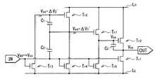
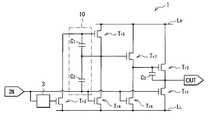
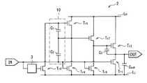
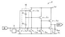
図1は、本発明の第1の実施の形態に係るインバータ回路1の全体構成の一例を表したものである。インバータ回路1は、入力端子INに入力されたパルス信号の信号波形(例えば図2(A))をほぼ反転させたパルス信号(例えば図2(B))を出力端子OUTから出力するものである。インバータ回路1は、アモルファスシリコンやアモルファス酸化物半導体上に好適に形成されるものであり、例えば、互いに同一のチャネル型の7つのトランジスタTr1〜Tr7を備えたものである。インバータ回路1は、上記の7つのトランジスタTr1〜Tr7の他に、3つの容量素子C1〜C3と、入力端子INおよび出力端子OUTとを備えており、7Tr3Cの回路構成となっている。<First Embodiment>
[Constitution]
FIG. 1 shows an example of the overall configuration of the inverter circuit 1 according to the first embodiment of the present invention. The inverter circuit 1 outputs a pulse signal (for example, FIG. 2B) obtained by substantially inverting the signal waveform (for example, FIG. 2A) of the pulse signal input to the input terminal IN from the output terminal OUT. . The inverter circuit 1 is suitably formed on amorphous silicon or an amorphous oxide semiconductor, and includes, for example, seven identical channel-type transistors Tr1 to Tr7 . The inverter circuit 1 includes three capacitance elements C1 to C3 , an input terminal IN, and an output terminal OUT in addition to theseven transistors Tr1 to Tr 7 described above, and has a 7Tr3C circuit configuration. Yes.
トランジスタTr1が本発明の「第1トランジスタ」の一具体例に相当し、トランジスタTr2が本発明の「第2トランジスタ」の一具体例に相当し、トランジスタTr3が本発明の「第3トランジスタ」の一具体例に相当する。また、トランジスタTr4が本発明の「第4トランジスタ」の一具体例に相当し、トランジスタTr5が本発明の「第5トランジスタ」の一具体例に相当する。また、トランジスタTr6が本発明の「第6トランジスタ」の一具体例に相当し、トランジスタTr7が本発明の「第7トランジスタ」の一具体例に相当する。また、容量素子C1が本発明の「第1容量素子」の一具体例に相当し、容量素子C2が本発明の「第2容量素子」の一具体例に相当し、容量素子C3が本発明の「第3容量素子」の一具体例に相当する。The transistor Tr1 corresponds to a specific example of the “first transistor” of the present invention, the transistor Tr2 corresponds to a specific example of the “second transistor” of the present invention, and the transistor Tr3 corresponds to the “third transistor” of the present invention. This corresponds to a specific example of “transistor”. The transistor Tr4 corresponds to a specific example of the “fourth transistor” of the present invention, and the transistor Tr5 corresponds to a specific example of the “fifth transistor” of the present invention. The transistor Tr6 corresponds to a specific example of “sixth transistor” of the present invention, and the transistor Tr7 corresponds to a specific example of “seventh transistor” of the present invention. The capacitive element C1 corresponds to a specific example of the “first capacitive element” of the present invention, the capacitive element C2 corresponds to a specific example of the “second capacitive element” of the present invention, and the capacitive element C3 Corresponds to a specific example of the “third capacitive element” of the present invention.
トランジスタTr1〜Tr7は、互いに同一チャネル型の薄膜トランジスタ(TFT)であり、例えば、nチャネルMOS(金属酸化膜半導体: Metal Oxide Semiconductor)型の薄膜トランジスタ(TFT)である。トランジスタTr1は、例えば、入力端子INの電圧(入力電圧Vin)と低電圧線LLの電圧VLとの電位差Vgs1(またはそれに対応する電位差)に応じて、出力端子OUTと低電圧線LLとの電気的な接続を継断するようになっている。トランジスタTr1のゲートが入力端子INに電気的に接続されており、トランジスタTr1のソースまたはドレインが低電圧線LLに電気的に接続されており、トランジスタTr1のソースおよびドレインのうち低電圧線LLに未接続の端子が出力端子OUTに電気的に接続されている。トランジスタTr2は、トランジスタTr7のソースまたはドレインのうち高電圧線LHに未接続の端子(端子A)の電圧Vs7と、出力端子OUTの電圧(出力電圧Vout)との電位差Vgs2(またはそれに対応する電位差)に応じて高電圧線LHと出力端子OUTとの電気的な接続を継断するようになっている。トランジスタTr2のゲートがトランジスタTr7の端子Aに電気的に接続されている。トランジスタTr2のソースまたはドレインが出力端子OUTに電気的に接続されており、トランジスタTr2のソースおよびドレインのうち出力端子OUTに未接続の端子が高電圧線LHに電気的に接続されている。The transistors Tr1 to Tr7 are thin film transistors (TFTs) of the same channel type, for example, n-channel MOS (Metal Oxide Semiconductor) type thin film transistors (TFTs). For example, the transistor Tr1 is connected to the output terminal OUT and the low voltage in accordance with a potential difference Vgs1 (or a corresponding potential difference) between the voltage at the input terminal IN (input voltage Vin ) and the voltage VL at the low voltage line LL. The electrical connection with the line LL is cut off. The gate of the transistor Tr1 is electrically connected to the input terminal IN, the source or drain of the transistor Tr1 is electrically connected to the low voltage line LL , and the transistor Tr1 has a low source and drain. A terminal not connected to the voltage line LL is electrically connected to the output terminal OUT. The transistor Tr2 has a potential difference Vgs2 between the voltage Vs7 of the terminal (terminal A) not connected to the high voltage line LH of the source or drain of the transistor Tr7 and the voltage of the output terminal OUT (output voltage Vout ). The electrical connection between the high voltage line LH and the output terminal OUT is cut off in accordance with (or a potential difference corresponding thereto). The gate of the transistor Tr2 is electrically connected to the terminal A of the transistor Tr7 . The source or drain of the transistor Tr2 is electrically connected to the output terminal OUT, and the terminal not connected to the output terminal OUT among the source and drain of the transistor Tr2 is electrically connected to the high voltage line LH. Yes.
トランジスタTr3は、入力電圧Vinと低電圧線LLの電圧VLとの電位差Vgs3(またはそれに対応する電位差)に応じてトランジスタTr5のゲートと低電圧線LLとの電気的な接続を継断するようになっている。トランジスタTr3のゲートが入力端子INに電気的に接続されている。トランジスタTr3のソースまたはドレインが低電圧線LLに電気的に接続されており、トランジスタTr3のソースおよびドレインのうち低電圧線LLに未接続の端子がトランジスタTr5のゲートに電気的に接続されている。トランジスタTr4は、入力電圧Vinと低電圧線LLの電圧VLとの電位差Vgs4(またはそれに対応する電位差)に応じてトランジスタTr5のソースおよびドレインのうち高電圧線LHに未接続の端子(端子B)と低電圧線LLとの電気的な接続を継断するようになっている。トランジスタTr4のゲートが入力端子INに電気的に接続されている。トランジスタTr4のソースまたはドレインが低電圧線LLに電気的に接続されており、トランジスタTr4のソースおよびドレインのうち低電圧線LLに未接続の端子がトランジスタTr5の端子Bに電気的に接続されている。トランジスタTr5は、容量素子C1の端子間電圧Vgs5(またはそれに対応する電位差)に応じて高電圧線LHと端子Bとの電気的な接続を継断するようになっている。トランジスタTr5のゲートがトランジスタTr3のソースおよびドレインのうち低電圧線LLに未接続の端子に電気的に接続されている。トランジスタTr5のソースまたはドレインが高電圧線LHに電気的に接続されている。トランジスタTr5のソースおよびドレインのうち高電圧線LHに未接続の端子(端子B)がトランジスタTr7のゲートと、トランジスタTr4のソースおよびドレインのうち低電圧線LLに未接続の端子とに接続されている。Transistor Tr3 is electrical the input voltage Vin the gate and the low-voltage line LL of the transistor Tr5 according to the potential difference Vgs3 the voltage VL of the low-voltage line LL (or the corresponding potential difference thereto) The connection is broken. The gate of the transistor Tr3 is electrically connected to the input terminal IN. The source or drain of the transistor Tr3 is electrically connected to the low-voltage line LL, the electrical terminal unconnected of the source and the drain of the transistor Tr3 to the low-voltage line LL is the gate of the transistor Tr5 It is connected to the. Transistor Tr4 is not yet in the high-voltage line LH of the source and the drain of the transistor Tr5 according to the potential difference VGS4 (or potential difference corresponding thereto) with the voltage VL of the input voltage Vin and the low-voltage line LL The electrical connection between the connection terminal (terminal B) and the low voltage line LL is interrupted. The gate of the transistor Tr4 is electrically connected to the input terminal IN. The source or drain of the transistor Tr4 is electrically connected to the low-voltage line LL, terminals unconnected of the source and the drain of the transistor Tr4 to the low-voltage line LL electrical terminal B of the transistor Tr5 Connected. The transistor Tr5cuts off the electrical connection between the high voltage line LH and the terminal B according to the inter-terminal voltage Vgs5 (or potential difference corresponding thereto) of the capacitive element C1 . The gate of the transistor Tr5 is electrically connected to a terminal not connected to the low voltage line LL among the source and drain of the transistor Tr3 . The source or drain of the transistor Tr5 is electrically connected to the high voltage line LH. A terminal (terminal B) that is not connected to the high voltage line LH among the source and drain of the transistor Tr5 is a terminal that is not connected to the low voltage line LL between the gate of the transistor Tr7 and the source and drain of the transistor Tr4. And connected to.
トランジスタTr6は、入力電圧Vinと低電圧線LLの電圧VLとの電位差Vgs6(またはそれに対応する電位差)に応じてトランジスタTr7のソースおよびドレインのうち高電圧線LHに未接続の端子(端子A)と低電圧線LLとの電気的な接続を継断するようになっている。トランジスタTr6のゲートが入力端子INに電気的に接続されている。トランジスタTr6のソースまたはドレインが低電圧線LLに電気的に接続されており、トランジスタTr6のソースおよびドレインのうち低電圧線LLに未接続の端子がトランジスタTr7の端子Aに電気的に接続されている。つまり、トランジスタTr1,Tr3,Tr4,Tr6は互いの同一の電圧線(低電圧線LL)に接続されている。従って、トランジスタTr1の低電圧線LL側の端子と、トランジスタTr3の低電圧線LL側の端子と、トランジスタTr4の低電圧線LL側の端子と、トランジスタTr6の低電圧線LL側の端子とは、互いに同電位となっている。トランジスタTr7は、トランジスタTr5のソースまたはドレインのうち高電圧線LHに未接続の端子(端子B)の電圧Vs5と、トランジスタTr2のゲート電圧Vg2との電位差Vgs7(またはそれに対応する電位差)に応じて高電圧線LHとトランジスタTr2のゲートとの電気的な接続を継断するようになっている。トランジスタTr7のゲートがトランジスタTr5の端子Bに電気的に接続されている。トランジスタTr7のソースまたはドレインがトランジスタTr2のゲートに電気的に接続されており、トランジスタTr7のソースおよびドレインのうちトランジスタTr2のゲートに未接続の端子が高電圧線LHに電気的に接続されている。つまり、トランジスタTr2,Tr5,Tr7は互いの同一の電圧線(高電圧線LH)に接続されている。従って、トランジスタTr2の高電圧線LH側の端子と、トランジスタTr5の高電圧線LH側の端子と、トランジスタTr7の高電圧線LH側の端子とは、互いに同電位となっている。Transistor Tr6 are not yet on the potential difference VGS6 high-voltage line LH of the source and the drain of the transistor Tr7 in response to (or potential difference corresponding thereto) with the voltage VL of the input voltage Vin and the low-voltage line LL The electrical connection between the connection terminal (terminal A) and the low voltage line LL is interrupted. The gate of the transistor Tr6 is electrically connected to the input terminal IN. The source or drain of the transistor Tr6 is electrically connected to the low-voltage line LL, terminals unconnected of the source and the drain of the transistor Tr6 to the low voltage line LL is electrically to the terminal A of the transistor Tr7 Connected. That is, the transistors Tr1 , Tr3 , Tr4 , and Tr6 are connected to the same voltage line (low voltage line LL ). Therefore, a low-voltage line LL terminal of the transistor Tr1, and the low-voltage line LL terminal of the transistor Tr3, and the low-voltage line LL of the transistor Tr4 terminals, low voltage of the transistor Tr6 The terminals on the line LL side are at the same potential. The transistor Tr7 has a potential difference Vgs7 (or a voltage difference between a voltage Vs5 of a terminal (terminal B) not connected to the high voltage line LH of the source or drain of the transistor Tr5 and a gate voltage Vg2 of the transistor Tr2 ). The electrical connection between the high voltage line LH and the gate of the transistor Tr2 is cut off according to the corresponding potential difference. The gate of the transistor Tr7 is electrically connected to the terminal B of the transistor Tr5 . The source or drain of the transistor Tr7 is electrically connected to the gate of the transistor Tr2, an electrical terminal unconnected to the gate of the transistor Tr2 of the source and the drain of the transistor Tr7 is in the high-voltage line LH It is connected to the. That is, the transistors Tr2 , Tr5 , Tr7 are connected to the same voltage line (high voltage line LH ). Accordingly, and the terminal of the high-voltage line LH side of the transistor Tr2, the terminal of the high voltage line LH side of the transistor Tr5, the terminal of the high voltage line LH side of the transistor Tr7 has a same potential ing.
低電圧線LLが本発明の「第1電圧線」、「第3電圧線」、「第4電圧線」、「第6電圧線」の一具体例に相当する。高電圧線LHが本発明の「第2電圧線」、「第5電圧線」、「第7電圧線」の一具体例に相当する。The low voltage line LL corresponds to a specific example of “first voltage line”, “third voltage line”, “fourth voltage line”, and “sixth voltage line” of the present invention. The high voltage line LH corresponds to a specific example of “second voltage line”, “fifth voltage line”, and “seventh voltage line” of the present invention.
高電圧線LHは、低電圧線LLの電圧VLよりも高電圧(一定電圧)を出力する電源(図示せず)に接続されている。高電圧線LHの電圧は、インバータ回路1の駆動時にVddとなっている。Vddは、入力端子INに印加される信号電圧(入力電圧Vin)のハイ電圧と同じ電圧値となっている。一方、低電圧線LLは、高電圧線LHの電圧VHよりも低電圧(一定電圧)を出力する電源(図示せず)に接続されており、低電圧線LLの電圧VLは、インバータ回路1の駆動時に電圧Vss(<Vdd1)となっている。The high voltage line LH is connected to a power supply (not shown) that outputs a higher voltage (constant voltage) than the voltage VL of the low voltage line LL. The voltage of the high voltage line LH is Vdd when the inverter circuit 1 is driven. Vdd has the same voltage value as the high voltage of the signal voltage (input voltage Vin ) applied to the input terminal IN. On the other hand, the low voltage line LL is connected to a power supply (not shown) that outputs a voltage (constant voltage) lower than the voltage VH of the high voltage line LH , and the voltage VL of the low voltage line LL Is a voltage Vss (<Vdd1 ) when the inverter circuit 1 is driven.
容量素子C1,C2は、入力端子INとトランジスタTr5のゲートとの間に直列に挿入されている。容量素子C1と容量素子C2との電気的な接続点Dが、トランジスタTr5の端子Bに電気的に接続されている。容量素子C1はトランジスタTr5のゲート側に挿入されており、容量素子C2はトランジスタTr1のゲート側に挿入されている。容量素子C2の容量は、容量素子C1の容量よりも大きくなっている。容量素子C1,C2のそれぞれの容量は、以下の式(1)を満たしていることが好ましい。容量素子C1,C2が数1を満たすならば、後述する入力電圧Vinが立ち下がった時、トランジスタTr5のゲート−ソース間電圧をその閾値電圧Vth5以上とすることができ、トランジスタTr5をオン状態とすることができる。その結果、出力電圧Voutがローからハイに変移することができる。
C2(Vdd−Vss)/(C1+C2)>Vth5…(1)The capacitive elements C1 and C2 are inserted in series between the input terminal IN and the gate of the transistor Tr5 . An electrical connection point D between the capacitive element C1 and the capacitive element C2 is electrically connected to a terminal B of the transistor Tr5 . The capacitive element C1 is inserted on the gate side of the transistor Tr5 , and the capacitive element C2 is inserted on the gate side of the transistor Tr1 . The capacitance of the capacitive element C2 is larger than the capacitance of the capacitive element C1 . The capacitances of the capacitive elements C1 and C2 preferably satisfy the following formula (1). If meeting the capacitive element C1, C2 is the number 1, when the fall of the input voltage Vin to be described later, the gate of the transistor Tr5 - can be the source voltage and the threshold voltage Vth5 above, transistor Tr5 can be turned on. As a result, the output voltage Vout can change from low to high.
C2 (Vdd −Vss ) / (C1 + C2 )> Vth5 (1)
ここで、容量素子C1,C2を含む回路部分は、インバータ回路1において、制御素子10を構成している。制御素子10は、例えば、図1に示したように、入力端子INに電気的に接続された端子P1、トランジスタTr5の端子Bに電気的に接続された端子P2、およびトランジスタTr5のゲートに電気的に接続された端子P3を有している。Here, the circuit portion including the capacitive elements C1 and C2 constitutes the
端子P1が、本発明の「第2端子」の一具体例に相当し、端子P2が、本発明の「第3端子」の一具体例に相当し、端子P3が、本発明の「第4端子」の一具体例に相当する。The terminal P1 corresponds to a specific example of the “second terminal” of the present invention, the terminal P2 corresponds to a specific example of the “third terminal” of the present invention, and the terminal P3 corresponds to the specific example of the present invention. This corresponds to a specific example of “fourth terminal”.
制御素子10は、例えば、端子P1に立下り電圧が入力されている時に端子P2のトランジェントを端子P3のトランジェントよりも緩やかにするようになっている。具体的には、制御素子10は、例えば、入力端子INに立下り電圧が入力されている時にトランジスタTr5のソースのトランジェントをトランジスタTr5のゲートのトランジェントよりも緩やかにするようになっている。なお、制御素子10の動作説明は、下記のインバータ回路1の動作説明と併せて行うものとする。トランジスタTr5のソースは、本発明の「第1端子」の一具体例に相当する。For example, when the falling voltage is input to the terminal P1 , the
ところで、インバータ回路1は、図35に示した参考例に係るインバータ回路600との関係では、出力段のトランジスタTr1,Tr2と、中段のトランジスタTr4,Tr5との間に、トランジスタTr6,Tr7と、容量素子C3とを挿入したものに相当する。このように、インバータ回路600において、トランジスタTr6,Tr7と、容量素子C3とを挿入することにより、後に詳述するように、トランジスタTr2,Tr5,Tr7のドレインに接続した電圧線を共通化することが可能となる。Incidentally, in the relationship with the inverter circuit 600 according to the reference example shown in FIG. 35, the inverter circuit 1 includes a transistor Tr between the output stage transistors Tr1 and Tr2 and the intermediate stage transistors Tr4 and Tr5.6 , Tr7 and a capacitor element C3 are inserted. As described above, by inserting the transistors Tr6 and Tr7 and the capacitor C3 in the inverter circuit 600, the voltage connected to the drains of the transistors Tr2 , Tr5 , and Tr7 as will be described in detail later. It is possible to share lines.
[動作]
次に、図3〜9を参照しつつ、インバータ回路1の動作の一例について説明する。図3は、インバータ回路1の動作の一例を表す波形図である。図4〜図9は、インバータ回路1の一連の動作の一例を表す回路図である。[Operation]
Next, an example of the operation of the inverter circuit 1 will be described with reference to FIGS. FIG. 3 is a waveform diagram illustrating an example of the operation of the inverter circuit 1. 4 to 9 are circuit diagrams illustrating an example of a series of operations of the inverter circuit 1.
まず、入力電圧Vinがハイ(Vdd)の時、トランジスタTr1,Tr3,Tr4,Tr6がオンする。すると、トランジスタTr2,Tr5,Tr7のゲート電圧Vg2,Vg5,Vg7およびソース電圧Vs2,Vs5,Vs7が低電圧線LLの電圧VL(=Vss)に充電される(図3、図4)。これにより、トランジスタTr2,Tr5,Tr7がオフ(Vgs2,Vgs5,Vgs7=0Vでオフする場合)し、電圧Vssが出力電圧Voutとして出力される。このとき、容量素子C2には、Vdd−Vssという電圧が充電される。First, the input voltage Vin is time high of (Vdd), the transistorsTr 1, Tr 3, Tr 4 ,
次に、入力電圧Vinがハイ(Vdd)からロー(Vss)に変化(低下)する時、トランジスタTr1,Tr3,Tr4,Tr6のゲート電圧Vg1,Vg3,Vg4,Vg6もVddからVssに変化(低下)する(図3、図5)。これにより、トランジスタTr1のゲート電圧Vg1の変化が容量素子C2を介してトランジスタTr7のゲートに伝播し、トランジスタTr7のゲート電圧Vg7がΔV1’だけ変化(低下)する。さらに、トランジスタTr1のゲート電圧Vg1の変化が容量素子C1,C2を介してトランジスタTr5のゲートにも伝播し、トランジスタTr5のゲート電圧Vg5がΔV2’だけ変化(低下)する。しかし、この時、トランジスタTr1,Tr3,Tr4,Tr6がオンしている。そのため、低電圧線LLからトランジスタTr2,Tr5,Tr7のソースおよびゲートに向かって電流が流れるので、その電流がそれらをVssに充電しようとする。Next, when the input voltage Vin is changed (reduced) from high (Vdd) to low (Vss), the transistorTr 1, Tr 3, Tr 4 , the gate voltage Vg1 of Tr6, Vg3, Vg4 , Vg6 also changes (decreases) from Vdd to Vss (FIGS. 3 and 5). As a result, the change in the gate voltage Vg1 of the transistor Tr1 propagates to the gate of the transistor Tr7 via the capacitive element C2, and the gate voltage Vg7 of the transistor Tr7 changes (decreases) by ΔV1 ′. Furthermore, the change in the gate voltage Vg1 of the transistor Tr1 is also propagated to the gate of the transistor Tr5 via the capacitive elements C1 and C2, and the gate voltage Vg5 of the transistor Tr5 changes (decreases) by ΔV2 ′. To do. However, at this time, the transistors Tr1 , Tr3 , Tr4 , and Tr6 are turned on. Therefore, since current flows from the low voltage line LL toward the sources and gates of the transistors Tr2 , Tr5 , Tr7 , the current tries to charge them to Vss .
ここで、トランジスタTr1,Tr3,Tr4,Tr6のゲート電圧はVddからVssに変化(低下)していくので、トランジスタTr1,Tr3,Tr4,Tr6のオン抵抗が徐々に大きくなり、トランジスタTr2,Tr5,Tr7のソースおよびゲートを低電圧線LLの電圧VLに充電するのに要する時間が長くなる。Here, since the gate voltages of the transistors Tr1 , Tr3 , Tr4 and Tr6 change (decrease) from Vdd to Vss , the on-resistances of the transistors Tr1 , Tr3 , Tr4 and Tr6 are reduced. It gradually increases, and the time required to charge the sources and gates of the transistors Tr2 , Tr5 , Tr7 to the voltage VL of the low voltage line LL becomes longer.
さらに、トランジスタTr5のソースおよびゲートから見える全容量を比較すると、トランジスタTr5のソースには容量素子C1,C2が並列接続され、トランジスタTr5のゲートには容量素子C1,C2が直列接続されている。このことから、トランジスタTr5のソースの方が、トランジスタTr5のゲートよりも、トランジェントが遅くなる。その結果、トランジスタTr5のソースを低電圧線LLの電圧VLに充電するのに要する時間の方がトランジスタTr5のゲートを低電圧線LLの電圧VLに充電するのに要する時間よりも長くなる。Furthermore, when comparing the total capacitance seen by the source and gate of the transistor Tr5, the capacitive element C1 to the source of the transistor Tr5, C2 are connected in parallel to the capacitive element C1 to the gate of the transistor Tr5, C2 Are connected in series. From this fact, towards the source of the transistor Tr5 is, than the gate of the transistor Tr5, transient is slow. As a result, the time required to charge the source of the transistor Tr5 to the voltage VL of the low voltage line LL is the time required to charge the gate of the transistor Tr5 to the voltage VL of the low voltage line LL. Longer than.
また、入力電圧VinがVss+Vth3以上となっており、さらに、Vss+Vth4以上となっている場合は、トランジスタTr3,Tr4は線形領域で動作する。なお、Vth3はトランジスタTr3の閾値電圧であり、Vth4はトランジスタTr4の閾値電圧である。一方、入力電圧VinがVss+Vth3未満となっており、さらに、Vss+Vth4未満となっている場合は、トランジスタTr3,Tr4は飽和領域で動作する。従って、トランジスタTr5のソースおよびゲートには、図5に示したような電流が流れるが、トランジスタTr3,Tr4は、それぞれの点を電圧Vssに充電することができない。The input voltage Vin has a Vss + Vth3 above, further, if that is the Vss + Vth4 or more, the transistor Tr3, Tr4 operates in a linear region. Vth3 is the threshold voltage of the transistor Tr3 , and Vth4 is the threshold voltage of the transistor Tr4 . On the other hand, the input voltage Vin has a less than Vss + Vth3, addition, if it is less than Vss + Vth4, transistors Tr3, Tr4 operates in the saturation region. Therefore, a current as shown in FIG. 5 flows through the source and gate of the transistor Tr5 , but the transistors Tr3 and Tr4 cannot charge each point to the voltage Vss .
最終的に、入力電圧VinがVddからVssになった時、トランジスタTr5のゲート−ソース間電圧Vgs5はΔV1−ΔV2となる(図3、図6)。このとき、トランジスタTr5のゲート−ソース間電圧Vgs5がトランジスタTr5の閾値電圧Vth5よりも大きくなった時点で、トランジスタTr5がオンし、高電圧線LHから電流が流れ始める。Finally, when the input voltage Vin becomes Vss from Vdd, the gate of the transistor Tr5 - source voltage VGS5 becomes ΔV1 -ΔV2 (FIG. 3, FIG. 6). At this time, the gate of the transistor Tr5 - source voltage VGS5 is when it becomes larger than the threshold voltage Vth5 of the transistor Tr5, the transistor Tr5 is turned on, current starts flowing from the high-voltage line LH.
トランジスタTr5がオンしている時は、トランジスタTr5のソース電圧Vs5は、トランジスタTr4に加えて、トランジスタTr5によっても上昇する。また、トランジスタTr5のゲート−ソース間には容量素子C1が接続されているので、ブートストラップが生じ、トランジスタTr5のゲート電圧Vg5も、トランジスタTr5のソース電圧Vs5の上昇に連動して上昇する。その後、トランジスタTr5のソース電圧Vs5およびゲート電圧Vg5がVss−Vth3以上となり、さらに、Vss−Vth4以上となった時点で、トランジスタTr3,Tr4がオフし、トランジスタTr5のソース電圧Vs5およびゲート電圧Vg5がトランジスタTr5のみによって上昇する。When the transistor Tr5 is on, the source voltage Vs5 of the transistor Tr5, in addition to the transistor Tr4, also increases the transistor Tr5. The gate of the transistor Tr5 - the capacitance element C1 between the source is connected, the bootstrap occurs, the gate voltage Vg5 of the transistor Tr5 is also linked to the increase in the source voltage Vs5 of the transistor Tr5 Then rise. After that, when the source voltage Vs5 and the gate voltage Vg5 of the transistor Tr5 become Vss −Vth3 or more and further become Vss −Vth4 or more, the transistors Tr3 and Tr4 are turned off, and the transistor Tr5 source voltage Vs5 and gate voltage Vg5 are raised only by transistor Tr5 .
一定時間経過後、トランジスタTr5のソース電圧Vg5(トランジスタTr7のゲート電圧Vs2)がVss+Vth7以上となると、トランジスタTr7がオンし、トランジスタTr7に電流が流れ始める(図3、図7)。なお、Vth7はトランジスタTr7の閾値電圧である。その結果、トランジスタTr7のソース電圧Vg7(トランジスタTr2のゲート電圧Vg2)は、Vssから徐々に上昇する。When the source voltage Vg5 of the transistor Tr5 (the gate voltage Vs2 of the transistor Tr7 ) becomesequal to or higher than Vss + Vth7 after a certain time has elapsed, the transistor Tr7 is turned on and a current starts to flow through the transistor Tr7 (FIG. 3). , FIG. 7). Vth7 is a threshold voltage of the transistor Tr7 . As a result, the source voltage Vg7 of the transistor Tr7 (the gate voltage Vg2 of the transistor Tr2 ) gradually increases from Vss .
ここで、トランジスタTr2のゲート電圧Vg2およびソース電圧Vs2について考える。トランジスタTr2のゲートソース間には、容量素子C3が接続されている。この容量素子C3によって、ブートストラップが生じ、トランジスタTr2のソース電圧Vs2とトランジスタTr2のゲート電圧Vg2とが連動して変化する。トランジスタTr2のゲート電圧Vg2はトランジスタTr7からの電流とトランジスタTr2のソース電圧Vs2の上昇とによって上昇する。そのため、トランジスタTr2の電流のみで上昇する場合と比べて、トランジスタTr2のゲートのトランジェントは速くなる。その結果、トランジスタTr2のゲートソース間電圧Vgs2は徐々に増加してゆく。Here, consider the gate voltage Vg2 and the source voltage Vs2 of the transistor Tr2 . A capacitive element C3 is connected between the gate and source of the transistor Tr2 . This capacitive element C3, bootstrap occurs, the gate voltage Vg2 of the source voltage Vs2 of the transistor Tr2 of the transistor Tr2 is changed in conjunction. The gate voltage of the transistor Tr2 Vg2 is increased by the increase in the source voltage Vs2 of the current and the transistor Tr2 from the transistor Tr7. Therefore, as compared with the case of increasing only the current of the transistor Tr2, transient gate of the transistor Tr2 is increased. As a result, the gate-source voltage Vgs2 of the transistor Tr2 gradually increases.
このとき、トランジスタTr7のゲート電圧Vg7は、トランジスタTr5がオンしているので、トランジスタTr7のソース電圧Vs7の上昇に追随せず、最終的に高電圧線LHの電圧VH(=Vdd)となる。これにより、トランジスタTr7からの電流はトランジスタTr2のゲート電圧Vg2(トランジスタTr7のソース電圧Vs7)の上昇と共に小さくなってゆく。トランジスタTr7のゲート−ソース間電圧Vgs7がトランジスタTr7の閾値電圧Vth7になった時を考えると、高電圧線LHから流れる電流はかなり小さくなり、トランジスタTr2のゲート電圧Vg2はトランジスタTr7の電流によって殆ど変化しなくなってしまう。しかし、このとき、トランジスタTr2はオン状態であり、トランジスタTr2のソース電圧Vs2は上昇しているので、ブートストラップ動作によってトランジスタTr2のゲート電圧Vg2も上昇を続ける。その結果、トランジスタTr7は完全にオフする。このとき、トランジスタTr2のゲート−ソース間電圧Vgs2がΔVxであったとする。そのとき、ΔVxがトランジスタTr2の閾値電圧Vth2よりも大きければ、トランジスタTr2のゲート電圧Vg2およびソース電圧Vs2は、トランジスタTr7がオフした後も上昇を続け、最終的に高電圧線LHの電圧VH(=Vdd)がVoutとして出力される(図3、図8)。At this time, the gate voltage Vg7 of the transistor Tr7, since the transistor Tr5 is on, does not follow the increase in the source voltage Vs7 of the transistor Tr7, finally the voltage VH of the high-voltage line LH (= Vdd ). Thus, the current from the transistor Tr7 is day become smaller with a rise in the gate voltage Vg2 of the transistor Tr2 (source voltage Vs7 of the transistor Tr7). The gate of the transistor Tr7 - source voltage VGS7 consider when it becomes the threshold voltage Vth7 of the transistor Tr7, the current flowing from the high-voltage line LH becomes considerably small, the gate voltage Vg2 of the transistor Tr2 is no longer change almost by the current of the transistor Tr7. However, this time, the transistor Tr2 is turned on, since the source voltage Vs2 of the transistor Tr2 has risen, it continues to rise also the gate voltage Vg2 of the transistor Tr2 by the bootstrap operation. As a result, the transistor Tr7 is completely turned off. At this time, it isassumed that the gate-source voltage Vgs2 of the transistor Tr2 is ΔVx . Then, if [Delta] Vx is greater than the threshold voltage Vth2 of the transistor Tr2, the gate voltage Vg2 and the source voltage Vs2 of the transistor Tr2 is also continued to rise after the transistor Tr7 is turned off, eventually high The voltage VH (= Vdd ) of the voltage line LH is output as Vout (FIGS. 3 and 8).
そして、さらに一定時間経過後、入力電圧Vinがロー(Vss)からハイ(Vdd1)に変化(上昇)する(図3、図9)。このとき、入力電圧VinがVss+Vth3よりも低くなっており、さらに、Vss+Vth4よりも低くなっている段階では、トランジスタTr3,Tr4はオフしている。そのため、容量素子C1,C2を介したカップリングがトランジスタTr5のソースおよびゲートに入力され、トランジスタTr5のソース電圧Vs5およびゲート電圧Vg5が上昇する。その後、入力電圧VinがVss+Vth1、Vss+Vth3、Vss+Vth6およびVss+Vth4以上となると、トランジスタTr1,Tr3,Tr4,Tr6がオンする。そのため、トランジスタTr2のソース(出力端子OUT)およびゲート、ならびにトランジスタTr5のソースおよびゲートに向かって電流が流れるので、その電流がそれらをVssに充電しようとする。Then, after further predetermined time, the input voltage Vin is changed from low (Vss) to high (Vdd1) (elevated) to (3, 9). At this time, the input voltage Vin is lower than Vss + Vth3, further, at the stage that is lower than Vss + Vth4, transistors Tr3, Tr4 are turned off. Therefore, the capacitive coupling elements C1, C2 is input to the source and gate of the transistor Tr5, the source voltage Vs5 and the gate voltage Vg5 of the transistor Tr5 is increased. Thereafter, when the input voltage Vin isV ss + V th1, V ss + V th3, V ss + V th6 and Vss + Vth4 above, the transistorsTr 1, Tr 3, Tr 4 ,
ここで、トランジスタTr1,Tr3,Tr4,Tr6のゲート電圧Vg1,Vg3,Vg4はVddからVssに変化(上昇)していくので、トランジスタTr1,Tr3,Tr4のオン抵抗が徐々に小さくなり、トランジスタTr2,Tr5のソースおよびゲートを低電圧線LLの電圧VLに充電するのに要する時間が相対的に短くなる。最終的に、トランジスタTr2のソース電圧Vs2、ならびにトランジスタTr5のソース電圧Vs5およびゲート電圧Vg5がVssとなり、出力端子からはVssが出力される(図3、図4)。Here, since the gate voltages Vg1 , Vg3 , Vg4 of the transistors Tr1 , Tr3 , Tr4 , Tr6 change (rise) from Vdd to Vss , the transistors Tr1 , Tr3 , Tr4 gradually decreases, and the time required to charge the sources and gates of the transistors Tr2 and Tr5 to the voltage VL of the low voltage line LL becomes relatively short. Finally, the source voltage Vs2 of the transistor Tr2 , the source voltage Vs5 and the gate voltage Vg5 of the transistor Tr5 become Vss , and Vss is output from the output terminal (FIGS. 3 and 4).
以上のようにして、本実施の形態のインバータ回路1では、入力端子INに入力されたパルス信号の信号波形(例えば図2(A))をほぼ反転させたパルス信号(例えば図2(B))が出力端子OUTから出力される。 As described above, in the inverter circuit 1 according to the present embodiment, the pulse signal (for example, FIG. 2B) obtained by substantially inverting the signal waveform (for example, FIG. 2A) of the pulse signal input to the input terminal IN. ) Is output from the output terminal OUT.
[効果]
ところで、例えば、図33に示したような従来のインバータ回路200は、2つのnチャネルMOS型のトランジスタTr1,Tr2が直列接続された単チャネル型の回路構成となっている。インバータ回路200では、例えば、図34に示したように、入力電圧VinがVssとなっている時、出力電圧VoutがVddとはならず、Vdd−Vth2となってしまう。つまり、出力電圧Voutには、トランジスタTr2の閾値電圧Vth2が含まれており、出力電圧Voutは、トランジスタTr2の閾値電圧Vth2のばらつきの影響を大きく受けてしまう。[effect]
Incidentally, for example, the conventional inverter circuit 200 as shown in FIG. 33 has a single-channel circuit configuration in which two n-channel MOS transistors Tr1 and Tr2 are connected in series. In the inverter circuit 200, for example, as shown in FIG. 34, when the input voltage Vin is Vss, not the output voltage Vout is Vdd, becomes Vdd -Vth2. That is, the output voltage Vout includes the threshold voltage Vth2 of the transistor Tr2 , and the output voltage Vout is greatly affected by variations in the threshold voltage Vth2 of the transistor Tr2 .
そこで、例えば、図35のインバータ回路300に示したように、トランジスタTr2のゲートとドレインとを互いに電気的に分離し、ドレインの電圧Vddよりも高い電圧Vdd2(≧Vdd+Vth2)が印加される高電圧配線LH2にゲートを接続することが考えられる。また、例えば、図36のインバータ回路400に示したようなブートストラップ型の回路構成が考えられる。Therefore, for example, as shown in the inverter circuit 300 of FIG. 35, the gate and the drain of the transistor Tr2 are electrically separated from each other, and the voltage Vdd2 (≧ Vdd + Vth2 ) higher than the drain voltage Vdd. It is conceivable to connect the gate to the high voltage wiring LH2 to which is applied. Further, for example, a bootstrap type circuit configuration as shown in the inverter circuit 400 of FIG. 36 is conceivable.
しかし、図33、図35、図36のいずれの回路においても、入力電圧Vinがハイとなっている時、つまり、出力電圧Voutがローとなっている時まで、トランジスタTr1,Tr2を介して、高電圧配線LH側から低電圧配線LL側に向かって電流(貫通電流)が流れてしまう。その結果、インバータ回路での消費電力も大きくなってしまう。また、図33、図35、図36の回路においては、例えば、図34(B)の破線で囲んだ箇所に示したように、入力電圧VinがVddとなっている時、出力電圧VoutがVssとはならず、出力電圧Voutの波高値がばらついてしまう。そのため、例えば、これらのインバータ回路を、アクティブマトリクス方式の有機EL表示装置におけるスキャナに用いた場合には、画素回路内の駆動トランジスタの閾値補正や移動度補正が画素回路ごとにばらついてしまい、そのばらつきが輝度のばらつきとなってしまうという。However, Figure 33, Figure 35, in any of the circuit of Figure 36, when the input voltage Vin is high, that is, until the output voltage Vout is in the low, transistors Tr1, Tr2 As a result, a current (through current) flows from the high voltage wiring LH side toward the low voltage wiring LL side. As a result, power consumption in the inverter circuit also increases. In the circuits of FIGS. 33, 35, and 36, for example, when the input voltage Vin is Vdd as shown in the portion surrounded by the broken line in FIG. 34B, the output voltage Vout does not become Vss, and the peak value of the output voltage Vout varies. Therefore, for example, when these inverter circuits are used in a scanner in an active matrix organic EL display device, threshold correction and mobility correction of the drive transistor in the pixel circuit vary from pixel circuit to pixel circuit. The variation becomes the luminance variation.
一方、本実施の形態のインバータ回路1では、トランジスタTr5のゲートと低電圧線LLとの間、トランジスタTr7のゲートと低電圧線LLとの間、トランジスタTr2のゲートと低電圧線LLとの間、トランジスタTr2のソースと低電圧線LLとの間には、入力電圧Vinと低電圧線LLの電圧VLとの電位差に応じてオンオフ動作するトランジスタTr1,Tr3,Tr4,Tr6が設けられている。これにより、トランジスタTr1,Tr3,Tr4,Tr6のそれぞれのゲート電圧がハイ(Vdd)からロー(Vss)に変移(低下)する時に、トランジスタTr1,Tr3,Tr4,Tr6のそれぞれのオン抵抗が徐々に大きくなり、トランジスタTr2,Tr5,Tr7のゲートおよびソースが低電圧線LLの電圧VLに充電されるのに要する時間が長くなる。さらに、トランジスタTr1,Tr3,Tr4,Tr6のそれぞれのゲート電圧がロー(Vss)からハイ(Vdd)に変移(上昇)する時に、トランジスタTr1,Tr3,Tr4,Tr6のそれぞれのオン抵抗が徐々に小さくなり、トランジスタTr2,Tr5,Tr7のゲートおよびソースが低電圧線LLの電圧VLに充電されるのに要する時間が短くなる。また、本発明では、入力端子INとトランジスタTr5のゲートとの間に、互いに直列に接続された第1容量素子および第2容量素子が挿入されている。さらに、トランジスタTr5のソースが、容量素子C1と容量素子C2との間に電気的に接続されている。これにより、トランジスタTr5のソースには、容量素子C1および容量素子C2が並列接続され、トランジスタTr5のゲートには、容量素子C1および容量素子C2が直列接続される。その結果、トランジスタTr5のソースの方が、トランジスタTr5のゲートよりも、トランジェントが遅くなる。これにより、トランジスタTr3、トランジスタTr4、トランジスタTr6およびトランジスタTr1のそれぞれのゲートが電圧がハイ(Vdd)からロー(Vss)に変移(低下)する時に、トランジスタTr5のゲート−ソース間電圧Vgs5がトランジスタTr5の閾値電圧Vth5よりも大きくなり、トランジスタTr5がオンし、その直後にトランジスタTr4がオフする。このとき、トランジスタTr7がオンするとともにトランジスタTr4がオフし、トランジスタTr2がオンするとともにトランジスタTr6がオフし、その後、トランジスタTr7がオフする。その結果、出力電圧Voutが高電圧線LH側の電圧となる。また、トランジスタTr3、トランジスタTr4、トランジスタTr6およびトランジスタTr1のそれぞれのゲートが電圧がロー(Vss)からハイ(Vdd)に変移(上昇)する時に、トランジスタTr3、トランジスタTr4、トランジスタTr6がオンし、その直後にトランジスタTr5がオフする。このとき、トランジスタTr2がオフするとともにトランジスタTr1がオンするので、出力電圧が第1電圧線側の電圧となる。On the other hand, in the inverter circuit 1 of the present embodiment, between the gate of the transistor Tr5 and the low voltage line LL , between the gate of the transistor Tr7 and the low voltage line LL, and between the gate of the transistor Tr2 and the low voltage line LL between line LL, between the source and the low voltage line LL of the transistor Tr2, the transistor Tr1 for turning on and off operation in response to a potential difference between the voltage VL of the input voltage Vin and the low-voltage line LL , Tr3 , Tr4 , Tr6 are provided. As a result, when the gate voltages of the transistors Tr1 , Tr3 , Tr4 , Tr6 change (decrease) from high (Vdd ) to low (Vss ), the transistors Tr1 , Tr3 , Tr4 , Each of the on-resistances of Tr6 gradually increases, and the time required for charging the gates and sources of the transistors Tr2 , Tr5 , Tr7 to the voltage VL of the low voltage line LL increases. Further, when the gate voltages of the transistors Tr1 , Tr3 , Tr4 , Tr6 change (rise) from low (Vss ) to high (Vdd ), the transistors Tr1 , Tr3 , Tr4 , Tr Each of the on-resistances of6 gradually decreases, and the time required for charging the gates and sources of the transistors Tr2 , Tr5 , Tr7 to the voltage VL of the low voltage line LL is shortened. In the present invention, between the gate of the input terminal IN and the transistor Tr5, the first capacitive element and the second capacitive element is inserted which is connected in series with each other. Further, the source of the transistor Tr5 is electrically connected between the capacitive element C1 and the capacitive element C2 . Thus, the source of the transistor Tr5, the capacitive element C1 and the capacitor C2 are connected in parallel, to the gate of the transistor Tr5, the capacitive element C1 and the capacitor C2 are connected in series. As a result, towards the source of the transistor Tr5 is, than the gate of the transistor Tr5, transient is slow. Thus, the transistor Tr3, the transistor Tr4, when each gate voltage of the transistor Tr6 and the transistor Tr1 is displaced (lowered) from high (Vdd) to low (Vss) to the gate of the transistor Tr5 - source voltage VGS5 is larger than the threshold voltage Vth5 of the transistor Tr5, the transistor Tr5 is turned on, the transistor Tr4 is turned off immediately thereafter. At this time, the transistor Tr4 is turned off with the transistor Tr7 is turned on, the transistor Tr6 the transistor Tr2 is turned on is turned off, then the transistor Tr7 is turned off. As a result, the output voltage Vout is the voltage of the high voltage line LH side. Further, when the gates of the transistors Tr3 , Tr4 , Tr6 and Tr1 change (rise) from low (Vss ) to high (Vdd ), the transistors Tr3 , Tr4 The transistor Tr6 is turned on, and immediately after that, the transistor Tr5 is turned off. At this time, since the transistor Tr2 is turned off and the transistor Tr1 is turned on, the output voltage becomes the voltage on the first voltage line side.
このように、本実施の形態のインバータ回路1では、トランジスタTr1とトランジスタTr2とが同時にオンしている期間や、トランジスタTr4とトランジスタTr5とが同時にオンしている期間、トランジスタTr6とトランジスタTr7とが同時にオンしている期間がほとんどないようにした。これにより、トランジスタTr1,Tr2、トランジスタTr4,Tr5、またはトランジスタTr6,Tr7を介して、高電圧線LHと低電圧線LLとの間を流れる電流(貫通電流)はほとんど存在しない。その結果、消費電力を抑えることができる。また、トランジスタTr1,Tr3,Tr4,Tr6のそれぞれのゲート電圧がハイ(Vdd)からロー(Vss)に変移(低下)したときに出力電圧Voutが高電圧線LH側の電圧となり、トランジスタTr1,Tr3,Tr4,Tr6のそれぞれのゲート電圧がロー(Vss)からハイ(Vdd)に変移(上昇)したときに出力電圧Voutが低電圧線LL側の電圧となるようにした。これにより、出力電圧Voutのばらつきをなくすことができる。その結果、例えば、画素回路内の駆動トランジスタの閾値補正や移動度補正の、画素回路ごとのばらつきを低減することができ、さらには画素ごとの輝度のばらつきを低減することができる。As described above, in the inverter circuit 1 of the present embodiment, the transistor Tr6 and the transistor Tr2 are turned on at the same time, the transistor Tr4 and the transistor Tr5 are turned on at the same time, and the transistor Tr6. And the transistor Tr7 are kept from being turned on at the same time. As a result, the current (through current) flowing between the high voltage line LH and the low voltage line LL via the transistors Tr1 , Tr2 , transistors Tr4 , Tr5 , or transistors Tr6 , Tr7 is reduced. Almost does not exist. As a result, power consumption can be suppressed. Further, when the gate voltages of the transistors Tr1 , Tr3 , Tr4 , and Tr6 change (decrease) from high (Vdd ) to low (Vss ), the output voltage Vout is on the high voltage line LH side. When the gate voltages of the transistors Tr1 , Tr3 , Tr4 , Tr6 change (rise) from low (Vss ) to high (Vdd ), the output voltage Vout becomes the low voltage line L The voltage was set to theL side. Thereby, the dispersion | variation in the output voltageVout can be eliminated. As a result, for example, variations in threshold correction and mobility correction of the drive transistor in the pixel circuit can be reduced for each pixel circuit, and further, luminance variations for each pixel can be reduced.
また、本実施の形態では、容量素子C1,C2が出力端子OUTに直接接続されていないので、トランジスタTr5のゲートおよびソースに入力されるカップリング量が出力段の寄生容量の影響を受けることがない。これにより、トランジスタTr5のゲート−ソース間電圧Vgs5を大きくすることができるので、インバータ回路1を高速化することができる。In the present embodiment, since the capacitive elements C1 and C2 are not directly connected to the output terminal OUT, the coupling amount input to the gate and source of the transistor Tr5 affects the influence of the parasitic capacitance of the output stage. I do not receive it. Thereby, since the gate-source voltage Vgs5 of the transistor Tr5 can be increased, the inverter circuit 1 can be speeded up.
また、本実施の形態では、インバータ回路1には低電圧側と高電圧側とで1つずつしか電圧線が設けられておらず、しかも、高電圧側の電圧線である高電圧線LHの電圧は、インバータ回路1の駆動時に、入力端子INに印加される信号電圧(入力電圧Vin)のハイ電圧と同じ電圧値(Vdd)となっている。従って、インバータ回路1の耐圧は、図33、図35、図36に示したような従来タイプのインバータ回路の耐圧と同様でよく、インバータ回路1の耐圧を上げる必要がない。これにより、インバータ回路1内の素子に耐圧の高いものを使う必要がなく、また、耐圧不具合による歩留まりの低下もないことから、製造コストを低く抑えることができる。In the present embodiment, the inverter circuit 1 is provided with only one voltage line for each of the low voltage side and the high voltage side, and the high voltage line LH that is a voltage line on the high voltage side. Is the same voltage value (Vdd ) as the high voltage of the signal voltage (input voltage Vin ) applied to the input terminal IN when the inverter circuit 1 is driven. Therefore, the withstand voltage of the inverter circuit 1 may be the same as that of the conventional type inverter circuit as shown in FIGS. 33, 35, and 36, and it is not necessary to increase the withstand voltage of the inverter circuit 1. As a result, it is not necessary to use a high breakdown voltage element in the inverter circuit 1 and there is no decrease in yield due to breakdown voltage problems, so that the manufacturing cost can be kept low.
また、本実施の形態では、インバータ回路1には最低限の数の電圧線しか設けられておらず、また、容量素子C2の容量を大きくしなくても、上述したようにインバータ回路1の高速化を実現することができる。これにより、例えば、有機EL表示装置において、インバータ回路1をスキャナなどに用いた場合に、表示パネルにおいて周囲(額縁)の占有面積を小さくすることができ、狭額縁化を実現することができる。Further, in this embodiment, only not provided minimum number of voltage lines to the inverter circuit 1 and also without increasing the capacitance of the capacitor C2, the inverter circuit 1 as described above High speed can be realized. Thereby, for example, in the organic EL display device, when the inverter circuit 1 is used for a scanner or the like, the area occupied by the periphery (frame) in the display panel can be reduced, and a narrowed frame can be realized.
<第2の実施の形態>
図10は、本発明の第2の実施の形態に係るインバータ回路2の全体構成の一例を表したものである。インバータ回路2は、上記実施の形態のインバータ回路1と同様、入力端子INに入力されたパルス信号の信号波形(例えば図2(A))をほぼ反転させたパルス信号(例えば図2(B))を出力端子OUTから出力するものである。インバータ回路2は、上記実施の形態のインバータ回路1において、容量素子C3の容量を大きくするとともに、出力端子OUTと低電圧線LLとの間に補助容量Csubを設けたものであり、それらの点で、上記実施の形態のインバータ回路1の構成と相違する。以下では、まず、上記実施の形態のインバータ回路1において生じ得る課題について説明し、その後で、本実施の形態のインバータ回路2の特徴部分について説明するものとする。なお、補助容量Csubは、本発明の「第4容量素子」の一具体例に相当する。<Second Embodiment>
FIG. 10 illustrates an example of the overall configuration of the
[課題]
上記実施の形態のインバータ回路1のトランジスタTr2のゲート電圧Vg2とソース電圧Vs2(出力電圧Vout)について考える。上述したように、トランジスタTr2のゲート電圧Vg2は、トランジスタTr7からの電流と、容量素子C3を介するトランジスタTr2のソース電圧Vs2の上昇とによって上昇する。このとき、トランジスタTr7からの電流は、トランジスタTr2のゲート電圧Vg2の上昇と共に減少してゆくので、トランジスタTr7がオフした後は、トランジスタTr2のゲート電圧Vg2はトランジスタTr2のソース電圧Vs2の上昇によってのみ上昇することになる。インバータ回路1において、トランジスタTr2のゲートには図11に示すような寄生容量Cgs2、Cgd2が存在する。そのため、トランジスタTr2のゲート電圧Vg2の変化量ΔVgは、トランジスタTr2のソース電圧Vs2の変化量ΔVsに対して、数1で示されるようにある一定の割合gで変化することとなる。この割合gをブートストラップゲインと呼ぶ。
Consider the gate voltage Vg2 and source voltage Vs2 (output voltage Vout ) of the transistor Tr2 of the inverter circuit 1 of the above embodiment. As described above, the gate voltage Vg2 of the transistor Tr2 is increased and the current from the transistor Tr7, by the rise of the source voltage Vs2 of the transistor Tr2 via a capacitor C3. At this time, the current from the transistor Tr7, since slide into decreases with increasing the gate voltage Vg2 of the transistor Tr2, the transistor Tr7 is after turned off, the gate voltage Vg2 of the transistor Tr2 is of the transistor Tr2 It rises only when the source voltage Vs2 rises. In the inverter circuit 1, the gate of the transistor Tr2 is present a parasitic capacitance Cgs2, Cgd2 as shown in FIG. 11. Therefore, the amount of change ΔVg of the gate voltage Vg2 of the transistor Tr2 becomes possible with respect to the change amount ΔVs of the source voltage Vs2 of the transistor Tr2, changes at a constant rate g in as indicated by the number 1 . This ratio g is called a bootstrap gain.
ここで、インバータ回路1の高速化を考えた場合、出力電圧Voutを出力するトランジスタTr1,Tr2のサイズを大きくすることが一般的である。トランジスタTr1を大きくした場合には、入力電圧Vinがロー(Vss)からハイ(Vdd)に変移(上昇)した時に、トランジスタTr1のゲート−ソース間に、より多くの電流を流すことができる。従って、トランジスタTr1を大きくした方が、出力電圧Voutの立下りのトランジェントが速くなる。Here, when speeding up the inverter circuit 1 is considered, it is common to increase the sizes of the transistors Tr1 and Tr2 that output the output voltage Vout . If you increase the transistor Tr1, upon transition (rising) to the input voltage Vin is low to high (Vss) (Vdd), the gate of the transistor Tr1 - between the source to flow more current be able to. Therefore, when the transistor Tr1 is made larger, the falling transient of the output voltage Vout becomes faster.
次に、トランジスタTr2のサイズを大きくした場合について考える。トランジスタTr2は、入力電圧Vinによって直接動作する訳ではなく、トランジスタTr7からの電流によって動作する。トランジスタTr7によってトランジスタTr2のゲート電圧Vg2が上昇すると、図12に示すようにトランジスタTr2のゲート−ソース間の容量Cgs2を介して出力端子OUTにカップリングが入力される。そのカップリング量(変化量ΔVs)は数2に示されるとおりである。
このとき、変化量ΔVgに対する変化量ΔVsの比率βを入力ゲインと呼ぶ。なお、図12には、出力端子OUTと低電圧線LLとの間に、寄生容量Coutが生じている様子が示されている。At this time, the ratio β of the change amount ΔVs to the change amount ΔVg is referred to as an input gain. FIG. 12 shows a state in which a parasitic capacitance Cout is generated between the output terminal OUT and the low voltage line LL.
トランジスタTr7によってトランジスタTr2のゲート−ソース間電圧Vgs2がその閾値電圧Vth2を超えた場合、トランジスタTr2から電流が流れ、出力電圧Voutは上昇する。トランジスタTr2のサイズが大きい場合、トランジスタTr2の電流駆動能力は高いので、トランジスタTr2のVgs2がVth2+Vaとなると、トランジスタTr2のソース電圧Vgs2は上昇を開始する。電圧Vaは、トランジスタTr2のサイズが大きいので、小さな値である。このとき、トランジスタTr2のゲート電圧Vg2の単位時間あたりの変化量に対して、トランジスタTr2のソース電圧Vs2の単位時間あたりの変化量(図13に示すグラフの傾き)が大きい場合、トランジスタTr2のゲート−ソース間電圧Vgs2は時間と共に小さくなってゆく。また、トランジスタTr2のゲート電圧Vg2がVdd−Vth7に近づくと、トランジスタTr2は自身の電流によってそのゲート電圧Vg2およびソース電圧Vs2を上昇させる。このとき、トランジスタTr2のゲート−ソース間電圧Vgs2はさらにブートストラップゲインgによって徐々に低下してゆく。The gate of the transistor Tr2 by transistor Tr7 - If the source voltage Vgs2 exceeds its threshold voltage Vth2, current flows from the transistor Tr2, the output voltage Vout rises. If the size of the transistor Tr2 is large, the high current driving capability of the transistor Tr2, when Vgs2 of the transistor Tr2 is Vth2 + Va, the source voltage Vgs2 of the transistor Tr2 starts to rise. Voltage Va is the size of the transistor Tr2 is large, a small value. At this time, with respect to the amount of change per unit time of the gate voltage Vg2 of the transistor Tr2, when the amount of change per unit time of the source voltage Vs2 of the transistor Tr2 (inclination of the graph shown in FIG. 13) is large, The gate-source voltage Vgs2 of the transistor Tr2 decreases with time. Further, the gate voltage Vg2 of the transistor Tr2 approaches the Vdd -Vth7, the transistor Tr2 raises the gate voltage Vg2 and the source voltage Vs2 by its own current. At this time, the gate-source voltage Vgs2 of the transistor Tr2 is gradually lowered by the bootstrap gain g.
したがって、電圧Vaの値が小さく、ブートストラップゲインgも小さい場合には、最終的に、トランジスタTr2のソース電圧Vs2がVddに到達する前にトランジスタTr2のゲート−ソース間電圧Vgs2がトランジスタTr2の閾値電圧Vth2となってしまう。そのため、トランジスタTr2のソース電圧Vs2はそれ以上上昇することができなくなる。その結果、トランジスタTr2はVddを出力することができない。Accordingly, small values of the voltage Va, when the bootstrap gain g is also small, ultimately, the gate of the transistor Tr2 before the source voltage Vs2 of the transistor Tr2 reaches the Vdd - source voltage Vgs2 becomes the threshold voltage Vth2 of the transistor Tr2. Therefore, the source voltage Vs2 of the transistor Tr2 can no longer rise. As a result, the transistor Tr2 can not output the Vdd.
この対策として、ブートストラップゲインgを上げるために容量素子C3の容量を大きくすることが考えられる。しかし、そのようにした場合には、入力ゲインが大きくなってしまう。入力ゲインが大きくなると、図14に示すように、トランジスタTr2のゲート−ソース間電圧Vgs2がトランジスタTr2の閾値電圧Vth2以下の時に、トランジスタTr2のゲート電圧Vg2の変化に対してソース電位Vs2が大きく上昇する。これにより、トランジスタTr2のソース電位Vs2が上昇を始める点が時間的に早まることとなる。その結果、トランジスタTr2のゲート電圧Vg2の変化があまり大きくない部分でトランジスタTr2のソース電圧Vs2は上昇を始めることとなり、トランジスタTr2は閾値補正を行ってしまう。つまり、トランジスタTr2のゲート電圧Vg2の変化量に対してソース電圧Vs2の変化量が大きく、トランジスタTr2のゲート−ソース間電圧Vgs2はどんどん小さくなり、最終的に閾値電圧Vth2という値となってしまう。従って、この場合でも、トランジスタTr2はVddを出力することができない。As a countermeasure, it is conceivable to increase the capacitance of the capacitive element C3 in order to increase the bootstrap gain g. However, in such a case, the input gain becomes large. When the input gain is increased, as shown in FIG. 14, the gate of the transistor Tr2 - source voltage Vgs2 is at equal to or less than the threshold voltage Vth2 of the transistor Tr2, with respect to the change of the gate voltage Vg2 of the transistor Tr2 The source potential Vs2 rises greatly. As a result, the point at which the source potential Vs2 of the transistor Tr2 starts to rise is advanced in time. As a result, the source voltage Vs2 of the transistor Tr2 in part the change in the gate voltage Vg2 of the transistor Tr2 is not so large becomes to start to rise, the transistor Tr2 would perform the threshold value correction. In other words, a large amount of change in the source voltage Vs2 relative to the amount of change in the gate voltage Vg2 of the transistor Tr2, the gate of the transistor Tr2 - source voltage Vgs2 becomes smaller and smaller, and finally that the threshold voltage Vth2 Value. Therefore, even in this case, the transistor Tr2 cannot output Vdd .
[インバータ回路2]
一方、本実施の形態のインバータ回路2では、容量素子C3の容量が大きくなっており、さらに出力端子OUTと低電圧線LLとの間に補助容量Csubが設けられている。[Inverter circuit 2]
On the other hand, in the
補助容量Csubが設けられている場合、ブートストラップゲインgには、数3に示したように、補助容量Csubの影響はない。その一方で、入力ゲインβには、数4に示したように、補助容量Csubが分母に入ることから、補助容量Csubによって入力ゲインβは小さくなる。
次に、インバータ回路2において、トランジスタTr2のサイズを大きくした場合について考える。補助容量Csubが出力端子OUTと低電圧線LLとの間に形成されることにより、図15に示すようにトランジスタTr2のソース電圧Vs2が上昇を開始する点は時間的に遅れる。このとき、上昇を開始した時のゲート−ソース間電圧Vgs2はVth2+Vbという値となる。Next, consider a case where the size of the transistor Tr2 is increased in the
ここで、Vb>Vaである。なぜなら、補助容量Csubが存在する場合と、存在しない場合とを対比すると、トランジスタTr2のソース電圧Vs2の変動量は、同じ大きさの電流が流れていても補助容量Csubが存在する場合の方が小さいからである。これは、補助容量Csubが存在しない場合には、補助容量Csubが存在する場合と同じだけのソース電圧Vs2の変動量を得るためにはトランジスタTr2のゲート−ソース間電圧Vgs2を大きくする必要があることに起因している。Here, Vb > Va . This is because, in the case where the auxiliary capacitance Csub is present, from a comparison with the absence, the variation amount of the source voltage Vs2 of the transistor Tr2 also have the same amount of current flow there is an auxiliary capacitance Csub This is because the case is smaller. This is because when the auxiliary capacitor Csub is not present, the gate-source voltage Vgs2 of the transistor Tr2 is set to obtain the same amount of variation of the source voltage Vs2 as when the auxiliary capacitor Csub is present. This is due to the need to enlarge.
このように、インバータ回路2では、ソース電圧Vs2の上昇開始点を遅らせて、Vbの値を大きくしている。これにより、トランジスタTr2からの電流やブートストラップゲインgによってトランジスタTr2のゲート−ソース間電圧Vgs2の値が小さくなったとしても、最終的に、トランジスタTr2のゲート−ソース間電圧Vgs2をその閾値電圧Vth2よりも大きな値に維持することができる。その結果、トランジスタTr2からVddという値を出力することができる。Thus, in the
<上記各実施の形態の変形例>
上記第2の実施の形態において、例えば、図16に示したように、容量素子C3をなくしてもよい。この場合、トランジスタTr2のゲート−ソース間には、寄生容量Cgs2が存在しており、その寄生容量Cgs2によるブートストラップゲインが存在する。そのため、補助容量Csubを設けるだけで、トランジスタTr2のゲート−ソース間電圧Vgs2を大きくすることができる。その結果、入力電圧Vinがロー(Vss)からハイ(Vdd)に変移(上昇)した時に、出力電圧Voutとして、Vddを出力することができる。<Modifications of the above embodiments>
In the second embodiment, for example, the capacitive element C3 may be eliminated as shown in FIG. In this case, a parasitic capacitance Cgs2 exists between the gate and source of the transistor Tr2 , and a bootstrap gain due to the parasitic capacitance Cgs2 exists. Therefore, the gate-source voltage Vgs2 of the transistor Tr2 can be increased only by providing the auxiliary capacitor Csub . As a result, when the input voltage Vin is shifted (raised) to high (Vdd) from low (Vss), as the output voltage Vout, it is possible to output a Vdd.
また、上記第2の実施の形態において、例えば、図17のインバータ回路4に示したように、トランジスタTr3,Tr5と、容量素子C1,C2をなくし、その代わりに、トランジスタTr8,Tr9と、容量素子C4を新たに設けてもよい。このインバータ回路4は、容量素子C4に保持された電荷をトランジスタTr7のゲートへ入力してトランジスタTr2のゲート電圧Vg2を上昇させ、出力電圧VoutとしてVddを出力するものである。In the second embodiment, for example, as shown in the inverter circuit 4 of FIG. 17, the transistors Tr3 and Tr5 and the capacitive elements C1 and C2 are eliminated, and instead the transistor Tr8 , Tr9 and a capacitive element C4 may be newly provided. This inverter circuit 4 inputs the electric charge held in the capacitive element C4 to the gate of the transistor Tr7 , raises the gate voltage Vg2 of the transistor Tr2 , and outputs Vdd as the output voltage Vout. .
トランジスタTr8,Tr9は、互いに同一チャネル型の薄膜トランジスタ(TFT)であり、例えば、nチャネルMOS型の薄膜トランジスタ(TFT)である。トランジスタTr8は、例えば、入力端子AZ1に入力される電圧と、容量素子C4の両端子のうち低電圧線LLに未接続の端子(端子E)の電圧との電位差Vgs8(またはそれに対応する電位差)に応じて、高電圧線LHと端子Eとの電気的な接続を継断するようになっている。トランジスタTr8のゲートが入力端子AZ1に電気的に接続されており、トランジスタTr8のソースまたはドレインが高電圧線LHに電気的に接続されており、トランジスタTr8のソースおよびドレインのうち高電圧線LHに未接続の端子が容量素子C4の端子Eに電気的に接続されている。トランジスタTr9は、入力端子AZ2に入力される電圧とトランジスタTr8のソースの電圧Vs8(端子Eの電圧)との電位差Vgs9(またはそれに対応する電位差)に応じて、トランジスタTr8のソース(端子E)とトランジスタTr7のゲートとの電気的な接続を継断するようになっている。トランジスタTr9のゲートが入力端子AZ2に電気的に接続されている。トランジスタTr9のソースまたはドレインがトランジスタTr8のソース(端子E)に電気的に接続されており、トランジスタTr9のソースおよびドレインのうち端子Eに未接続の端子がトランジスタTr7のゲートに電気的に接続されている。The transistors Tr8 and Tr9 are the same channel type thin film transistors (TFTs), for example, n channel MOS type thin film transistors (TFTs). For example, the transistor Tr8 has a potential difference Vgs8 (or a voltage difference between a voltage input to the input terminal AZ1 and a voltage of a terminal (terminal E) not connected to the low voltage line LL among both terminals of the capacitive element C4 ). according to the corresponding potential difference), which makes or breaks electrical connection between the high-voltage line LH and the terminal E. The gate of the transistor Tr8 is electrically connected to the input terminal AZ1, the source or drain of the transistor Tr8 is electrically connected to the high voltage line LH , and the higher of the source and drain of the transistor Tr8 A terminal not connected to the voltage line LH is electrically connected to the terminal E of the capacitive element C4 . The transistor Tr9 has the source of the transistor Tr8 in accordance with the potential difference Vgs9 (or a potential difference corresponding thereto) between the voltage input to the input terminal AZ2 and the source voltage Vs8 (voltage of the terminal E) of the transistor Tr8 . The electrical connection between the (terminal E) and the gate of the transistor Tr7 is cut off. The gate of the transistor Tr9 is electrically connected to the input terminal AZ2. The source or drain of the transistor Tr9 is electrically connected to the source (terminal E) of the transistor Tr8 , and the terminal not connected to the terminal E among the source and drain of the transistor Tr9 is electrically connected to the gate of the transistor Tr7. Connected.
入力端子AZ1には、例えば、図18(B)に示したようなパルス信号が印加される。入力端子AZ2には、例えば、図18(C)に示したように、入力端子AZ1に印加されるパルス信号と逆位相のパルス信号が印加される。これにより、出力電圧VoutとしてVddを出力することができる。For example, a pulse signal as shown in FIG. 18B is applied to the input terminal AZ1. For example, as shown in FIG. 18C, a pulse signal having a phase opposite to that of the pulse signal applied to the input terminal AZ1 is applied to the input terminal AZ2. Thereby,Vdd can be output as the output voltageVout .
また、上記各実施の形態において、例えば、図19、図20、図21に示したように、入力端子INとトランジスタTr3のゲートの間に、遅延素子3を設けてもよい。In the above embodiments, for example, 19, 20, as shown in FIG. 21, between the input terminal IN and the transistor Tr3 gates may be provided a
遅延素子3は、入力端子OUTに入力された信号電圧の電圧波形を鈍らせた電圧をトランジスタTr3のゲートに入力するものである。遅延素子3は、例えば、電圧波形の立ち下がりを、入力端子OUTに入力された信号電圧の電圧波形の立ち下がりよりも緩やかにした電圧をトランジスタTr3のゲートに入力するようになっている。なお、遅延素子3は、電圧波形の立ち下がりだけでなく、立ち上がりについても、入力端子OUTに入力された信号電圧の電圧波形の立ち上がりよりも緩やかにするようになっていてもよい。ただし、その場合には、遅延素子3は、立ち下がりの方が立ち上がりよりも、より緩やかになるように、入力端子OUTに入力された信号電圧の電圧波形を鈍らせるようになっている。Delay
遅延素子3は、例えば、図22(A)〜(D)に示した回路構成となっている。図22(A)においては、遅延素子3は、容量素子C5を含んで構成されている。容量素子C5の一端がトランジスタTr3のゲートに電気的に接続されており、容量素子C5の他端が低電圧線LLに電気的に接続されている。The
図22(B)においては、遅延素子3はトランジスタTr10を含んで構成されている。トランジスタTr10は、トランジスタTr1等のチャネル型と同一チャネル型のトランジスタであり、例えば、nチャネルMOS型のTFTである。トランジスタTr10のソースがトランジスタTr3のゲートに電気的に接続されており、トランジスタTr10のドレインが入力端子INに電気的に接続されている。トランジスタTr10のゲートは高電圧線LH3に電気的に接続されている。高電圧線LH3は、トランジスタTr10をオンオフ動作させるパルス信号を出力する電源(図示せず)に電気的に接続されている。In FIG. 22 (B), the
図22(C)においては、遅延素子3は、上述のトランジスタTr10と、トランジスタTr11とを含んで構成されている。トランジスタTr11は、トランジスタTr1等のチャネル型と同一チャネル型のトランジスタであり、例えば、nチャネルMOS型のTFTである。トランジスタTr11のゲートおよびソースがトランジスタTr3のゲートに電気的に接続されており、トランジスタTr11のドレインが入力端子INに電気的に接続されている。In FIG. 22C, the
図22(D)においては、遅延素子3は、上述のトランジスタTr10と、上述の容量素子C5とを含んで構成されている。In FIG. 22D, the
[動作・効果]
図23は、本変形例に係るインバータ回路の動作の一例を表したものである。なお、図23には、遅延素子3として、図22(D)に示した回路構成を有するものが用いられたときの波形が示されている。本変形例に係るインバータ回路の基本的な動作は、図3〜図8に示すものと同様である。図3〜図8に示すものと相違する箇所は、入力電圧Vinがハイ(Vdd)からロー(Vss)に変移(低下)するときと、ロー(Vss)からハイ(Vdd)に変移(上昇)するときにある。[Operation / Effect]
FIG. 23 shows an example of the operation of the inverter circuit according to this modification. FIG. 23 shows waveforms when the
入力電圧Vinがハイ(Vdd)からロー(Vss)に変移(低下)するとき、トランジスタTr3,Tr4のゲート電圧はVddからVssへ変化する。上記実施の形態のインバータ回路1,2では、この電圧変化が、容量素子C2を介してトランジスタTr5のソースへΔV1という電圧変化を生じさせ、さらに容量素子C1,C2を介してトランジスタTr5のゲートへΔV2という電圧変化を生じさせていた。ここで、トランジスタTr5のゲートにΔV2というカップリング量が入力されていたのは、トランジスタTr3のゲート電圧VがVddからVssに低下してゆき、その結果、トランジスタTr3のオン抵抗が徐々に増加し、トランジスタTr5のゲートをVssに充電するトランジェントが遅くなるからである。換言すると、トランジスタTr5のゲートにΔV2というカップリング量が入力されるのは、カップリングが入力されるタイミングでトランジスタTr3がオンからオフに切り替わるからである。When the input voltage Vin is displaced (lowered) from high (Vdd) to low (Vss), the gate voltage of the transistor Tr3, Tr4 changes from Vdd to Vss. In the
一方、本変形例では、遅延素子3によって、入力端子INに入力された信号電圧を図24に示したように鈍らせた信号電圧がトランジスタTr3のゲートに入力される。これにより、トランジスタTr3のオフ点(オンとオフが切り替わる点)が入力電圧VinをそのままトランジスタTr3のゲートに入力した場合と比べて遅くなる。つまり、トランジスタTr3は、容量素子C2を介したカップリングが入力されるタイミングでもオンしていることになる(図25)。そのため、最終的にトランジスタTr5のゲートに入力されるカップリング量(ΔV2)を従来よりも小さくすることができ、トランジスタTr5のゲートソース間電圧Vgs5を大きくすることが可能となる。その結果、インバータ回路の高速化が実現できる。On the other hand, in this modification, the signal voltage obtained by blunting the signal voltage input to the input terminal IN as shown in FIG. 24 by the
本変形例では、入力電圧Vinがロー(Vss)からハイ(Vdd)に変移(上昇)する場合でも、トランジスタTr3のゲートには、遅延素子3によって、入力端子INに入力された信号電圧を図24に示したように鈍らせた信号電圧が入力される。そのため、トランジスタTr3のオフ点が遅くなるので、トランジスタTr1がオンした後にトランジスタTr3がオンすることとなり、出力電圧Voutが遷移状態である時に高電圧線LHから低電圧線LLへ電流(貫通電流)が流れる可能性がある。しかし、実際には、トランジスタTr3のオンする動作点と、トランジスタTr3のゲートに入力される信号電圧の波形とを考えると、トランジスタTr3のゲートに入力される信号電圧の遅延によっても、図25に示すように立ち上りにおいてはトランジスタTr3のオンする時間は殆ど変わらず、逆に立ち下がりにおいてはオフする時間が大きく変化する。そのため、上述した貫通電流が流れる期間は非常に微小であり、本変形例に係るインバータ回路の消費電力は、インバータ回路1,2の消費電力とあまり変わらない。In this modification, the input voltage Vin even when low transition (rising) from (Vss) to high (Vdd), to the gate of the transistor Tr3 is the
ところで、上記各実施の形態では、トランジスタTr5のソースおよびゲートに、入力電圧Vinの変化に起因するカップリングを入力し、トランジスタTr5のソースおよびゲートにおけるトランジェントの差を利用して、トランジスタTr5のゲート−ソース間電圧Vgs5をトランジスタTr5の閾値電圧Vth5以上の値にしている。このとき、出力端子OUTには、高電圧線LH側の電圧が出力電圧Voutとして出力されるが、出力端子OUTのトランジェントは、トランジスタTr2のゲート−ソース間電圧Vgs2に大きく依存する。つまり、トランジスタTr2のゲート−ソース間電圧Vgs2が早く大きくなる場合は、出力電圧Voutが早く立ち上がり、トランジスタTr2のゲート−ソース間電圧Vgs2がゆっくり大きくなる場合は、出力電圧Voutの立ち上がりもゆっくりとなる。Incidentally, in the above embodiments, the source and gate of the transistor Tr5, enter the coupling caused by a change in the input voltage Vin, by utilizing the difference in transients at the source and the gate of the transistor Tr5, transistor the gate of the Tr5 - has a source voltage VGS5 to the threshold voltage Vth5 or more values of the transistor Tr5. At this time, the voltage on the high voltage line LH side is output to the output terminal OUT as the output voltage Vout , but the transient of the output terminal OUT greatly depends on the gate-source voltage Vgs2 of the transistor Tr2. . That is, when the gate-source voltage Vgs2 of the transistor Tr2 quickly increases, the output voltage Vout rises quickly, and when the gate V-source voltage Vgs2 of the transistor Tr2 increases slowly, the output voltage Vout Rises slowly.
そこで、インバータ回路を高速化する際にはトランジスタTr2のゲート−ソース間電圧Vgs2を早く立ち上げればよいことになるが、その方法として、例えば、容量素子C2の容量を大きくすることが考えられる。しかし、容量素子C2の容量を大きくした場合には、インバータ回路の占有面積が大きくなってしまう。その結果、例えば、有機EL表示装置において、容量素子C2の容量を大きくしたインバータ回路をスキャナなどに用いた場合は、表示パネルにおいて周囲(額縁)の占有面積が大きくなってしまい、狭額縁化を阻害してしまう虞がある。また、容量素子C2の容量を大きくした場合には、トランジスタTr2のソース(出力端子OUT)に、ΔV1よりも大きな電圧変化が生じるが、その分、トランジスタTr2のゲートにも、ΔV2よりも大きな電圧変化が生じる。その結果、トランジスタTr2のゲート−ソース間電圧Vgs2は、容量素子C2の容量を大きくした割りに、ΔV1−ΔV2とさほど変わらない値となってしまい、容量素子C2の容量増大がインバータ回路1の高速化にあまり寄与しない。Therefore, when the speed of the inverter circuit is increased, the gate-source voltage Vgs2 of the transistor Tr2 may beraised quickly. As a method for this, for example, the capacitance of the capacitive element C2 is increased. Conceivable. However, in the case of increasing the capacitance of the capacitor C2 is the area occupied by the inverter circuit is increased. As a result, for example, in the organic EL display device, in the case of using an inverter circuit having an increased capacitance of the capacitor C2, etc. to the scanner, becomes large area occupied by the peripheral (frame) in the display panel, frame narrowing May be disturbed. Further, when increasing the capacitance of the capacitor C2 is the source of the transistor Tr2 (output terminal OUT), although a large voltage change than [Delta] V1 occurs, correspondingly, to the gate of the transistor Tr2, [Delta] VA voltage change greater than2 occurs. As a result, the gate of the transistor Tr2 - source voltage Vgs2 are largely the dividing the capacitance of the capacitor C2, becomes a much unchanged value as [Delta] V1 - [Delta] V2, increasing the capacitance of the capacitor C2 However, it does not contribute much to the speeding up of the inverter circuit 1.
一方、本変形例では、遅延素子3によって、入力端子INに入力された信号電圧を図24に示したように鈍らせた信号電圧がトランジスタTr3のゲートに入力される。これにより、容量素子C2の容量を増大させることなく、インバータ回路の高速化が実現できる。On the other hand, in this modification, the signal voltage obtained by blunting the signal voltage input to the input terminal IN as shown in FIG. 24 by the
また、上記各実施の形態およびそれらの変形例では、トランジスタTr1〜Tr11が、nチャネルMOS型のTFTにより形成されていたが、例えば、pチャネルMOS型のTFTにより形成されていてもよい。ただし、この場合には、高電圧線LHが低電圧線LLに置き換えられ、高電圧線LHが低電圧線LLに置き換えられる。また、トランジスタTr1〜Tr11がローからハイに変移(上昇)する時の過渡応答と、トランジスタTr1〜Tr11がハイからローに変移(下降)する時の過渡応答とが互いに逆となる。In each of the above-described embodiments and their modifications, the transistors Tr1 to Tr11 are formed of n-channel MOS type TFTs, but may be formed of, for example, p-channel MOS type TFTs. . However, in this case, the high voltage line LH is replaced with the low voltage line LL , and the high voltage line LH is replaced with the low voltage line LL. The transistor Tr1 to Tr11 is the transient response at the time of transition (rising) from low to high, the transient response and is opposite to each other when the transistor Tr1 to Tr11 is displaced (lowered) from high to low .
<第3の実施の形態>
図26は、本発明の第3の実施の形態に係るインバータ回路3の全体構成の一例を表したものである。インバータ回路3は、インバータ回路1との関係では、容量素子C1を削除し、トランジスタTr7のゲート−ソース間に容量素子C6を追加したものに相当する。また、インバータ回路3は、インバータ回路1との関係では、トランジスタTr5のゲートと、トランジスタTr3のソースまたはドレインとを、抵抗R1を介して高電圧線LHに接続したものに相当する。さらに、インバータ回路3は、インバータ回路1との関係では、低電圧線LLを2つの低電圧線LL1,LL2に分け、一方の低電圧線LL1をトランジスタTr1,Tr4,Tr5に接続し、他方の低電圧線LL2を、抵抗R2を介してトランジスタTr3のソースおよびドレインのうち抵抗R1に未接続の端子に接続したものに相当する。なお、抵抗R2は、トランジスタTr3のオン抵抗を含んだものであり、具体的には、トランジスタTr3がオンしたときにトランジスタTr5のゲート電圧Vg5がトランジスタTr5のオン電圧より小さくなるような値となっている。<Third Embodiment>
FIG. 26 illustrates an example of the overall configuration of the
[動作・効果]
入力電圧Vinがハイ(Vdd)のときは、トランジスタTr3はオンしている。そのため、トランジスタTr5のゲート電圧Vg5は、高電圧線LHおよび低電圧線LL2の電位差を、抵抗R1,R2のそれぞれの抵抗値で分圧した値で決まる。例えば、高電圧線LHの電圧が15V、低電圧線LL2の電圧が−6Vとなっているとき、トランジスタTr5のゲート電圧Vg5は、1Vとなっている。このとき、トランジスタTr4もオンしているので、トランジスタTr7のゲート電圧Vg7は、低電圧線LL1の電圧Vss(例えば0V)となっている。各トランジスタTr1〜Tr7の閾値電圧が2Vとなっているとすると、トランジスタTr2,Tr5,Tr7は全て、オフしており、出力端子OUTからは低電圧線LL1の電圧と等しい電圧が出力される。[Operation / Effect]
When the input voltage Vin is high of (Vdd), the transistor Tr3 is turned on. Therefore, the gate voltage Vg5 of the transistor Tr5 is the potential difference between the high-voltage line LH and the low-voltage line LL2, determined by the resistance values of the resistors R1, R2 obtained by dividing the value. For example, when the voltage of the high-voltage line LH is 15V, the voltage of the low-voltage line LL2 it has become -6 V, the gate voltage Vg5 of the transistor Tr5 has a 1V. At this time, since the transistor Tr4 is also turned on, the gate voltage Vg7 of the transistor Tr7 has a voltage Vss of the low-voltage line LL1 (e.g., 0V). Assuming that the threshold voltage of each of the transistors Tr1 to Tr7 is 2V, all of the transistors Tr2 , Tr5 , and Tr7 are off and are equal to the voltage of the low voltage line LL1 from the output terminal OUT. Voltage is output.
入力電圧Vinがロー(Vss)になると、トランジスタTr7のゲート電圧Vg7は、容量素子C6,C2のカップリングによって低下する。このとき、トランジスタTr3はオフするので、トランジスタTr5のゲート電圧Vg5は、抵抗R1を通じてゆっくり上昇し、これにより、トランジスタTr5がオンし、続けて、トランジスタTr2,Tr7もオンする。その結果、出力端子OUTから、高電圧線LHの電圧と等しい電圧が出力される。When the input voltage Vin is low (Vss), the gate voltage Vg7 of the transistor Tr7 is reduced by the coupling of the capacitor C6, C2. At this time, since the transistor Tr3 is turned off, the gate voltage Vg5 of the transistor Tr5 is slowly increased through the resistor R1, Thus, the transistor Tr5 is turned on, followed by the transistors Tr2, Tr7 also on To do. As a result, from the output terminal OUT, and a voltage equal to the voltage of the high-voltage line LH is outputted.
このように、本実施の形態では、入力電圧Vinがハイ(Vdd)のときに、低電圧線LL1の電圧と等しい電圧が出力端子OUTから出力され、入力電圧Vinがロー(Vss)のときに、高電圧線LHの電圧と等しい電圧が出力端子OUTから出力される。これにより、出力電圧Voutのばらつきをなくすことができる。従って、例えば、インバータ回路3をディスプレイパネルのスキャナーに適用することにより、スキャナーの出力ばらつきをなくすることができ、その結果、画素のラインごとの輝度のばらつきを抑えることができる。Thus, in this embodiment, when the input voltage Vin is high in (Vdd), a voltage equal to the voltage of the low-voltage line LL1 is output from the output terminal OUT, and the input voltage Vin is low (V when thess), a voltage equal to the voltage of the high-voltage line LH is output from the output terminal OUT. Thereby, the dispersion | variation in the output voltageVout can be eliminated. Therefore, for example, by applying the
また、本実施の形態では、容量素子C6,C2が出力端子OUTに直接接続されていないので、トランジスタTr7のゲートおよびソースに入力されるカップリング量が出力段の寄生容量の影響を受けることがない。これにより、トランジスタTr7のゲート−ソース間電圧Vgs7を大きくすることができるので、インバータ回路5を高速化することができる。In the present embodiment, since the capacitive elements C6 and C2 are not directly connected to the output terminal OUT, the coupling amount input to the gate and source of the transistor Tr7 affects the influence of the parasitic capacitance of the output stage. I do not receive it. As a result, the gate-source voltage Vgs7 of the transistor Tr7 can be increased, so that the
また、本実施の形態では、インバータ回路5には低電圧側に2つの電圧線、高電圧側に1つの電圧線しか設けられておらず、しかも、高電圧側の電圧線である高電圧線LHの電圧は、インバータ回路1の駆動時に、入力端子INに印加される信号電圧(入力電圧Vin)のハイ電圧と同じ電圧値(Vdd)となっている。従って、インバータ回路5の耐圧は、図33、図35、図36に示したような従来タイプのインバータ回路の耐圧と同様でよく、インバータ回路1の耐圧を上げる必要がない。これにより、インバータ回路5内の素子に耐圧の高いものを使う必要がなく、また、耐圧不具合による歩留まりの低下もないことから、製造コストを低く抑えることができる。Further, in the present embodiment, the
また、本実施の形態では、インバータ回路5には最低限の数の電圧線しか設けられておらず、また、容量素子C2の容量を大きくしなくても、上述したようにインバータ回路5の高速化を実現することができる。これにより、例えば、有機EL表示装置において、インバータ回路5をスキャナなどに用いた場合に、表示パネルにおいて周囲(額縁)の占有面積を小さくすることができ、狭額縁化を実現することができる。In the present embodiment, the
<適用例>
図28は、上記各実施の形態およびそれらの変形例に係るインバータ回路1,2,4,5の適用例の一例である表示装置100の全体構成の一例を表したものである。この表示装置100は、例えば、表示パネル110(表示部)と、駆動回路120(駆動部)とを備えている。<Application example>
FIG. 28 illustrates an example of the overall configuration of the
(表示パネル110)
表示パネル110は、発光色の互いに異なる3種類の有機EL素子111R,111G,111Bが2次元配置された表示領域110Aを有している。表示領域110Aとは、有機EL素子111R,111G,111Bから発せられる光を利用して映像を表示する領域である。有機EL素子111Rは赤色光を発する有機EL素子であり、有機EL素子111Gは緑色光を発する有機EL素子であり、有機EL素子111Bは青色光を発する有機EL素子である。なお、以下では、有機EL素子111R,111G,111Bの総称として有機EL素子111を適宜、用いるものとする。(Display panel 110)
The
(表示領域110A)
図29は、表示領域10A内の回路構成の一例を、後述の書込線駆動回路124の一例と共に表したものである。表示領域110A内には、複数の画素回路112が個々の有機EL素子111と対となって2次元配置されている。なお、本適用例では、一対の有機EL素子111および画素回路112が1つの画素113を構成している。より詳細には、図28に示したように、一対の有機EL素子111Rおよび画素回路112が1つの赤色用の画素113Rを構成し、一対の有機EL素子111Gおよび画素回路112が1つの緑色用の画素113Gを構成し、一対の有機EL素子111Bおよび画素回路112が1つの青色用の画素113Bを構成している。さらに、互いに隣り合う3つの画素113R,113G,113Bが1つの表示画素114を構成している。(
FIG. 29 illustrates an example of a circuit configuration in the
各画素回路112は、例えば、有機EL素子111に流れる電流を制御する駆動トランジスタTr100と、信号線DTLの電圧を駆動トランジスタTr100に書き込む書き込みトランジスタTr200と、保持容量Csとによって構成されたものであり、2Tr1Cの回路構成となっている。駆動トランジスタTr100および書き込みトランジスタTr200は、例えば、nチャネルMOS型の薄膜トランジスタ(TFT)により形成されている。駆動トランジスタTr100または書き込みトランジスタTr200は、例えば、pチャネルMOS型のTFTであってもよい。Each
表示領域110Aにおいて、複数の書込線WSL(走査線)が行状に配置され、複数の信号線DTLが列状に配置されている。表示領域110Aには、さらに、複数の電源線PSL(電源電圧の供給される部材)が書込線WSLに沿って行状に配置されている。各信号線DTLと各書込線WSLとの交差点近傍には、有機EL素子111が1つずつ設けられている。各信号線DTLは、後述の信号線駆動回路123の出力端(図示せず)と、書き込みトランジスタTr200のドレイン電極およびソース電極のいずれか一方(図示せず)に接続されている。各書込線WSLは、後述の書込線駆動回路124の出力端(図示せず)と、書き込みトランジスタTr200のゲート電極(図示せず)に接続されている。各電源線PSLは、後述の電源線駆動回路125の出力端(図示せず)と、駆動トランジスタTr100のドレイン電極およびソース電極のいずれか一方(図示せず)に接続されている。書き込みトランジスタTr200のドレイン電極およびソース電極のうち信号線DTLに未接続の方(図示せず)は、駆動トランジスタTr100のゲート電極(図示せず)と、保持容量Csの一端に接続されている。駆動トランジスタTr100のドレイン電極およびソース電極のうち電源線PSLに未接続の方(図示せず)と保持容量Csの他端とが、有機EL素子111のアノード電極(図示せず)に接続されている。有機EL素子111のカソード電極(図示せず)は、例えば、グラウンド線GNDに接続されている。In the
(駆動回路120)
次に、駆動回路120内の各回路について、図28、図29を参照して説明する。駆動回路120は、タイミング生成回路121、映像信号処理回路122、信号線駆動回路123、書込線駆動回路124、および電源線駆動回路125を有している。(Drive circuit 120)
Next, each circuit in the
タイミング生成回路121は、映像信号処理回路122、信号線駆動回路123、書込線駆動回路124、および電源線駆動回路125が連動して動作するように制御するものである。タイミング生成回路121は、例えば、外部から入力された同期信号120Bに応じて(同期して)、上述した各回路に対して制御信号121Aを出力するようになっている。 The
映像信号処理回路122は、外部から入力された映像信号120Aに対して所定の補正を行うと共に、補正した後の映像信号122Aを信号線駆動回路123に出力するようになっている。所定の補正としては、例えば、ガンマ補正や、オーバードライブ補正などが挙げられる。 The video
信号線駆動回路123は、制御信号121Aの入力に応じて(同期して)、映像信号処理回路122から入力された映像信号122A(信号電圧Vsig)を各信号線DTLに印加して、選択対象の画素113に書き込むものである。なお、書き込みとは、駆動トランジスタTr1のゲートに所定の電圧を印加することを指している。In response to (in synchronization with) the input of the
信号線駆動回路123は、例えばシフトレジスタ(図示せず)を含んで構成されており、画素113の各列に対応して、1段ごとにバッファ回路(図示せず)を備えている。この信号線駆動回路123は、制御信号121Aの入力に応じて(同期して)、各信号線DTLに対して、2種類の電圧(Vofs、Vsig)を出力可能となっている。具体的には、信号線駆動回路123は、各画素113に接続された信号線DTLを介して、書込線駆動回路124により選択された画素113へ2種類の電圧(Vofs、Vsig)を順番に供給するようになっている。The signal
ここで、オフセット電圧Vofsは、信号電圧Vsigの値に依らず一定電圧値となっている。また、信号電圧Vsigは、映像信号122Aに対応する電圧値となっている。信号電圧Vsigの最小電圧はオフセット電圧Vofsよりも低い電圧値となっており、信号電圧Vsigの最大電圧はオフセット電圧Vofsよりも高い電圧値となっている。Here, the offset voltage Vofs is a constant voltage value regardless of the value of the signal voltage Vsig . The signal voltage Vsig is a voltage value corresponding to the
書込線駆動回路124は、例えば、図30に示したように、シフトレジスタSRおよびインバータINVが交互に接続されたユニットと、このユニット内のインバータINVの出力に接続されたバッファ回路6とを含んで構成されている。バッファ回路6は、画素113の各行に対応して、1段ずつ設けられている。上記のユニットは、シフトレジスタSRに入力される同期パルスCk(図示せず)によって、入力転送パルスStを1H遅らせて、後段のインバータINVに転送するようになっている。インバータINVは、入力パルスを反転するとともに、その波形を整形し、後段のシフトレジスタSRに転送するようになっている。書込線駆動回路124は、この一連の動きを、例えば表示パネル110の縦の画素数分だけ行うようになっている。 For example, as shown in FIG. 30, the write
バッファ回路6は、上述したインバータ回路1,2,4,5を複数含んで構成されたものであり、入力端に入力されたパルス信号の位相とほぼ同一位相のパルス信号を出力端から出力するものである。書込線駆動回路124は、制御信号121Aの入力に応じて(同期して)、各書込線WSLに対して、2種類の電圧(Vdd、Vss)を出力可能となっている。具体的には、書込線駆動回路124は、各画素113に接続された書込線WSLを介して、駆動対象の画素113へ2種類の電圧(Vdd、Vss)を供給し、書き込みトランジスタTr200を制御するようになっている。The
ここで、電圧Vddは、書き込みトランジスタTr200のオン電圧以上の値となっている。Vddは、後述の消光時や閾値補正時に、書込線駆動回路124から出力される電圧値である。Vssは、書き込みトランジスタTr200のオン電圧よりも低い値となっており、かつ、Vddよりも低い値となっている。Here, the voltage Vdd is a value equal to or higher than the ON voltage of the write transistor Tr200 . Vdd is a voltage value output from the write
電源線駆動回路125は、例えばシフトレジスタ(図示せず)を含んで構成されており、例えば、画素113の各行に対応して、1段ごとにバッファ回路(図示せず)を備えている。この電源線駆動回路125は、制御信号121Aの入力に応じて(同期して)、2種類の電圧(VccH、VccL)を出力可能となっている。具体的には、電源線駆動回路125は、各画素113に接続された電源線PSLを介して、駆動対象の画素113へ2種類の電圧(VccH、VccL)を供給し、有機EL素子111の発光および消光を制御するようになっている。The power supply
ここで、電圧VccLは、有機EL素子111の閾値電圧Velと、有機EL素子111のカソードの電圧Vcaとを足し合わせた電圧(Vel+Vca)よりも低い電圧値である。また、電圧VccHは、電圧(Vel+Vca)以上の電圧値である。Here, the voltage VccL is a voltage value lower than a voltage (Vel + Vca ) obtained by adding the threshold voltage Vel of the
次に、本適用例の表示装置100の動作(消光から発光までの動作)の一例について説明する。本適用例では、駆動トランジスタTr100の閾値電圧Vthや移動度μが経時変化したりしても、それらの影響を受けることなく、有機EL素子111の発光輝度を一定に保つようにするために、閾値電圧Vthや移動度μの変動に対する補正動作が組み込まれている。Next, an example of the operation (operation from extinction to light emission) of the
図31は、画素回路112に印加される電圧波形の一例と、駆動トランジスタTr100のゲート電圧Vgおよびソース電圧Vsの変化の一例とを表したものである。図31(A)には信号線DTLに、信号電圧Vsigと、オフセット電圧Vofsが印加されている様子が示されている。図31(B)には書込線WSLに、書き込みトランジスタTr200をオンする電圧Vddと、書き込みトランジスタTr200をオフする電圧Vssが印加されている様子が示されている。図31(C)には電源線PSLに、電圧VccHと、電圧VccLが印加されている様子が示されている。さらに、図31(D),(E)には、電源線PSL、信号線DTLおよび書込線WSLへの電圧印加に応じて、駆動トランジスタTr100のゲート電圧Vgおよびソース電圧Vsが時々刻々変化している様子が示されている。FIG. 31 shows an example of a voltage waveform applied to the
(Vth補正準備期間)
まず、Vth補正の準備を行う。具体的には、書込線WSLの電圧がVoffとなっており、電源線DSLの電圧がVccHとなっている時(つまり有機EL素子111が発光している時)に、電源線駆動回路125が電源線DSLの電圧をVccHからVccLに下げる(T1)。すると、ソース電圧VsがVccLとなり、有機EL素子111が消光する。その後、信号線DTLの電圧がVofsとなっている時に書込線駆動回路124が書込線WSLの電圧をVoffからVonに上げ、駆動トランジスタTr100のゲートをVofsとする。(Vth correction preparation period)
First, preparation for Vth correction is performed. Specifically, when the voltage of the write line WSL is Voff and the voltage of the power line DSL is VccH (that is, when the
(最初のVth補正期間)
次に、Vthの補正を行う。具体的には、書込みトランジスタTr200がオンしており、信号線DTLの電圧がVofsとなっている間に、電源線駆動回路125が電源線DSLの電圧をVccLからVccHに上げる(T2)。すると、駆動トランジスタTr100のドレイン−ソース間に電流Idsが流れ、ソース電圧Vsが上昇する。その後、信号線駆動回路123が信号線DTLの電圧をVofsからVsigに切り替える前に、書込線駆動回路124が書込線WSLの電圧をVonからVoffに下げる(T3)。すると、駆動トランジスタTr100のゲートがフローティングとなり、Vthの補正が休止する。(First Vth correction period)
Next, Vth is corrected. More specifically, it turned writing transistor Tr200 is, while the voltage of the signal line DTL is Vofs, the power supply
(最初のVth補正休止期間)
Vth補正が休止している期間中は、例えば、先のVth補正を行った行(画素)とは異なる他の行(画素)において、信号線DTLの電圧のサンプリングが行われる。なお、このとき、先のVth補正を行った行(画素)において、ソース電圧VsがVofs−Vthよりも低いので、Vth補正休止期間中にも、先のVth補正を行った行(画素)において、駆動トランジスタTr100のドレイン−ソース間に電流Idsが流れ、ソース電圧Vsが上昇し、保持容量Csを介したカップリングによりゲート電圧Vgも上昇する。(First Vth correction pause period)
During the period in which the Vth correction is paused, for example, the voltage of the signal line DTL is sampled in another row (pixel) that is different from the row (pixel) that has been subjected to the previous Vth correction. At this time, in the line from which the previous Vth correction (pixels), since the source voltage Vs is lower than Vofs -Vth, even during the Vth correction stop period, subjected to previous Vth correction in Tagyo (pixels), the drain of the driving transistor Tr100 - current Ids flows between the source, the source voltage Vs is increased, the gate voltage Vg by coupling through the storage capacitor Cs is also increased.
(2回目のVth補正期間)
次に、Vth補正を再び行う。具体的には、信号線DTLの電圧がVofsとなっており、Vth補正が可能となっている時に、書込線駆動回路124が書込線WSLの電圧をVoffからVonに上げ、駆動トランジスタTr100のゲートをVofsにする(T4)。このとき、ソース電圧VsがVofs−Vthよりも低い場合(Vth補正がまだ完了していない場合)には、駆動トランジスタTr100がカットオフするまで(ゲート−ソース間電圧VgsがVthになるまで)、駆動トランジスタTr100のドレイン−ソース間に電流Idsが流れる。その後、信号線駆動回路123が信号線DTLの電圧をVofsからVsigに切り替える前に、書込線駆動回路124が書込線WSLの電圧をVonからVoffに下げる(T5)。すると、駆動トランジスタTr100のゲートがフローティングとなるので、ゲート−ソース間電圧Vgsを信号線DTLの電圧の大きさに拘わらず一定に維持することができる。(Second Vth correction period)
Next, Vth correction is performed again. Specifically, when the voltage of the signal line DTL is Vofs and Vth correction is possible, the write
なお、このVth補正期間において、保持容量CsがVthに充電され、ゲート−ソース間電圧VgsがVthとなった場合には、駆動回路120は、Vth補正を終了する。しかし、ゲート−ソース間電圧VgsがVthにまで到達しない場合には、駆動回路120は、ゲート−ソース間電圧VgsがVthに到達するまで、Vth補正と、Vth補正休止とを繰り返し実行する。In this Vth correction period, when the storage capacitor Cs is charged to Vth and the gate-source voltage Vgs becomes Vth , the
(書き込み・μ補正期間)
Vth補正休止期間が終了した後、書き込みとμ補正を行う。具体的には、信号線DTLの電圧がVsigとなっている間に、書込線駆動回路124が書込線WSLの電圧をVoffからVonに上げ(T6)、駆動トランジスタTr1のゲートを信号線DTLに接続する。すると、駆動トランジスタTr100のゲート電圧Vgが信号線DTLの電圧Vsigとなる。このとき、有機EL素子111のアノード電圧はこの段階ではまだ有機EL素子111の閾値電圧Velよりも小さく、有機EL素子111はカットオフしている。そのため、電流Idsは有機EL素子111の素子容量(図示せず)に流れ、素子容量が充電されるので、ソース電圧VsがΔVyだけ上昇し、やがてゲート−ソース間電圧VgsがVsig+Vth−ΔVyとなる。このようにして、書き込みと同時にμ補正が行われる。ここで、駆動トランジスタTr100の移動度μが大きい程、ΔVyも大きくなるので、ゲート−ソース間電圧Vgsを発光前にΔVyだけ小さくすることにより、画素113ごとの移動度μのばらつきを取り除くことができる。(Writing / μ correction period)
After the end of the Vth correction pause period, writing and μ correction are performed. Specifically, while the voltage of the signal line DTL is Vsig, the write
(発光期間)
最後に、書込線駆動回路124が書込線WSLの電圧をVonからVoffに下げる(T7)。すると、駆動トランジスタTr100のゲートがフローティングとなり、駆動トランジスタTr100のドレイン−ソース間に電流Idsが流れ、ソース電圧Vsが上昇する。その結果、有機EL素子111に閾値電圧Vel以上の電圧が印加され、有機EL素子111が所望の輝度で発光する。(Light emission period)
Finally, the write
本適用例の表示装置100では、上記のようにして、各画素113において画素回路112がオンオフ制御され、各画素113の有機EL素子111に駆動電流が注入されることにより、正孔と電子とが再結合して発光が起こり、その光が外部に取り出される。その結果、表示パネル110の表示領域110Aにおいて画像が表示される。 In the
ところで、本適用例では、例えば、書込線駆動回路124内のバッファ回路6は、上述したインバータ回路1,2,4を複数含んで構成されている。これにより、バッファ回路6内を流れる貫通電流はほとんど存在しないので、バッファ回路6の消費電力を抑えることができる。また、バッファ回路6の出力電圧のばらつきが少ないので、画素回路112内の駆動トランジスタTr100の閾値補正や移動度補正の、画素回路112ごとのばらつきを低減することができ、さらには画素113ごとの輝度のばらつきを低減することができる。By the way, in this application example, for example, the
以上、実施の形態、変形例および適用例を挙げて本発明を説明したが、本発明は実施の形態等に限定されるものではなく、種々変形が可能である。 The present invention has been described with the embodiment, the modification, and the application example. However, the present invention is not limited to the embodiment and the like, and various modifications can be made.
例えば、上記各実施の形態およびそれらの変形例では、高電圧側の電圧線および低電圧側の電圧線がそれぞれ1本ずつ設けられていたが、例えば、高電圧側の複数のトランジスタのうち少なくとも1つと接続された電圧線が、他の高電圧側のトランジスタに接続された電圧線と非共有となっていてもよい。同様に、例えば、低電圧側の複数のトランジスタのうち少なくとも1つと接続された電圧線が、他の低電圧側のトランジスタに接続された電圧線と非共有となっていてもよい。 For example, in each of the above-described embodiments and their modifications, one high-voltage side voltage line and one low-voltage side voltage line are provided. The voltage line connected to one may not be shared with the voltage line connected to the other transistor on the high voltage side. Similarly, for example, a voltage line connected to at least one of a plurality of transistors on the low voltage side may not be shared with a voltage line connected to another transistor on the low voltage side.
また、例えば、上記適用例では、上記各実施の形態に係るインバータ回路1,2,4が書込線駆動回路124の出力段に用いられていたが、書込線駆動回路124の出力段の代わりに、電源線駆動回路125の出力段に用いられていてもよいし、書込線駆動回路124の出力段と共に、電源線駆動回路125の出力段に用いられていてもよい。 Further, for example, in the application example, the
1,2,4,5,200,300,400,500,600…インバータ回路、3…遅延素子、6…バッファ回路、10…制御素子、100…表示装置、110…表示パネル、110A…表示領域、111,111R,111G,111B…有機EL素子、112…画素回路、113,113R,113G,113B…画素、114…表示画素、120…駆動回路、120A,122A…映像信号、120B…同期信号、121…タイミング生成回路、121A…制御信号、122…映像信号処理回路、123…信号線駆動回路、124…書込線駆動回路、125…電源線駆動回路、A,B,E,P1,P2,P3,…端子、C,D…接続点、C1〜C5…容量素子、Cs…保持容量、DTL…信号線、GND…グラウンド線、IN,AZ1,AZ2…入力端子、Ids…電流、LH,LH1,LH2…高電圧線、LL,LL1,LL2…低電圧線、OUT…出力端子、P…WSパルス、PSL…電源線、Tr1〜Tr12…トランジスタ、Tr100…駆動トランジスタ、Tr200…書き込みトランジスタ、VCCH,VCCL,Vdd,Vdd2,VH,VL,Vss,Vy,ΔV1’,ΔV2’,ΔV1,ΔV2…電圧、Vg,Vg1〜Vg5…ゲート電圧、Vgs,Vgs,Vgs2,Vgs5…ゲート−ソース間電圧、ΔVg,ΔVs…変化量、Vin…入力電圧、Vofs…オフセット電圧、Vout…出力電圧、Vs,Vs2,Vs5…ソース電圧、Vsig…信号電圧、Vth,Vth1〜Vth5,Vel…閾値電圧、WSL…書込線、μ…移動度、ΔVx…カップリング量。1, 2, 4, 5, 200, 300, 400, 500, 600 ... inverter circuit, 3 ... delay element, 6 ... buffer circuit, 10 ... control element, 100 ... display device, 110 ... display panel, 110A ...
Claims (19)
Translated fromJapanese第1容量素子、第2容量素子および第3容量素子と、
入力端子および出力端子と
を備え、
前記第1トランジスタは、前記入力端子の電圧と第1電圧線の電圧との電位差またはそれに対応する電位差に応じて前記出力端子と前記第1電圧線との電気的な接続を継断するようになっており、
前記第2トランジスタは、当該第2トランジスタのゲート電圧と、前記出力端子の電圧との電位差またはそれに対応する電位差に応じて第2電圧線と前記出力端子との電気的な接続を継断するようになっており、
前記第3トランジスタは、前記入力端子の電圧と第3電圧線の電圧との電位差またはそれに対応する電位差に応じて前記第5トランジスタのゲートと前記第3電圧線との電気的な接続を継断するようになっており、
前記第4トランジスタは、前記入力端子の電圧と第4電圧線の電圧との電位差またはそれに対応する電位差に応じて前記第5トランジスタのソースまたはドレインである第1端子と前記第4電圧線との電気的な接続を継断するようになっており、
前記第1容量素子および前記第2容量素子は、前記入力端子と前記第5トランジスタのゲートとの間に直列に挿入されており、
前記第1容量素子と前記第2容量素子との電気的な接続点が、前記第1端子に電気的に接続されており、
前記第3容量素子は、前記第2トランジスタのゲートと前記出力端子との間に挿入されており、
前記第5トランジスタは、前記第1容量素子の端子間電圧またはそれに対応する電圧に応じて第5電圧線と前記第1端子との電気的な接続を継断するようになっており、
前記第6トランジスタは、前記入力端子の電圧と第6電圧線の電圧との電位差またはそれに対応する電位差に応じて前記第2トランジスタのゲートと前記第6電圧線との電気的な接続を継断するようになっており、
前記第7トランジスタは、前記第1端子の電圧と前記第2トランジスタのゲート電圧との電位差またはそれに対応する電位差に応じて第7電圧線と前記第2トランジスタのゲートとの電気的な接続を継断するようになっている
インバータ回路。A first transistor, a second transistor, a third transistor, a fourth transistor, a fifth transistor, a sixth transistor, and a seventh transistor of the same channel type;
A first capacitive element, a second capacitive element and a third capacitive element;
With input and output terminals,
The first transistor disconnects the electrical connection between the output terminal and the first voltage line according to a potential difference between the voltage of the input terminal and the voltage of the first voltage line or a corresponding potential difference. And
The second transistor interrupts the electrical connection between the second voltage line and the output terminal according to a potential difference between the gate voltage of the second transistor and the voltage of the output terminal or a potential difference corresponding thereto. And
The third transistor cuts off the electrical connection between the gate of the fifth transistor and the third voltage line according to a potential difference between the voltage of the input terminal and the voltage of the third voltage line or a corresponding potential difference. Is supposed to
The fourth transistor has a potential difference between a voltage of the input terminal and a voltage of the fourth voltage line or a corresponding potential difference between the first terminal which is the source or drain of the fifth transistor and the fourth voltage line. It is designed to cut off the electrical connection,
The first capacitive element and the second capacitive element are inserted in series between the input terminal and the gate of the fifth transistor,
An electrical connection point between the first capacitive element and the second capacitive element is electrically connected to the first terminal;
The third capacitive element is inserted between the gate of the second transistor and the output terminal;
The fifth transistor is adapted to cut off the electrical connection between the fifth voltage line and the first terminal according to the voltage between the terminals of the first capacitive element or the voltage corresponding thereto.
The sixth transistor interrupts electrical connection between the gate of the second transistor and the sixth voltage line according to a potential difference between the voltage of the input terminal and the voltage of the sixth voltage line or a corresponding potential difference. Is supposed to
The seventh transistor has an electrical connection between the seventh voltage line and the gate of the second transistor according to a potential difference between the voltage of the first terminal and the gate voltage of the second transistor or a corresponding potential difference. Inverter circuit that is supposed to be cut off.
第1容量素子、第2容量素子および第3容量素子と、
入力端子および出力端子と
を備え、
前記第1トランジスタのゲートは前記入力端子に電気的に接続され、前記第1トランジスタのドレインまたはソースは第1電圧線に電気的に接続され、前記第1トランジスタのドレインおよびソースのうち前記第1電圧線に未接続の端子は前記出力端子に電気的に接続され、
前記第2トランジスタのゲートは前記第7トランジスタのドレインまたはソースに電気的に接続され、前記第2トランジスタのドレインまたはソースは第2電圧線に電気的に接続され、前記第2トランジスタのドレインおよびソースのうち前記第2電圧線に未接続の端子は前記出力端子に電気的に接続され、
前記第3トランジスタのゲートは前記入力端子に電気的に接続され、前記第3トランジスタのドレインまたはソースは第3電圧線に電気的に接続され、前記第3トランジスタのドレインおよびソースのうち前記第3電圧線に未接続の端子は前記第5トランジスタのゲートに電気的に接続され、
前記第4トランジスタのゲートは前記入力端子に電気的に接続され、前記第4トランジスタのドレインまたはソースは第4電圧線に電気的に接続され、前記第4トランジスタのドレインおよびソースのうち前記第4電圧線に未接続の端子は前記第7トランジスタのゲートに電気的に接続され、
前記第5トランジスタのドレインまたはソースは第5電圧線に電気的に接続され、前記第5トランジスタのドレインおよびソースのうち前記第5電圧線に未接続の端子は前記第7トランジスタのゲートに電気的に接続され、
前記第6トランジスタのゲートは前記入力端子に電気的に接続され、前記第6トランジスタのドレインまたはソースは第6電圧線に電気的に接続され、前記第6トランジスタのドレインおよびソースのうち前記第6電圧線に未接続の端子は前記第2トランジスタのゲートに電気的に接続され、
前記第7トランジスタのドレインまたはソースは第7電圧線に電気的に接続され、前記第7トランジスタのドレインおよびソースのうち前記第7電圧線に未接続の端子は前記第2トランジスタのゲートに電気的に接続され、
前記第1容量素子および前記第2容量素子は、前記入力端子と前記第5トランジスタのゲートとの間に直列に挿入され、
前記第1容量素子と前記第2容量素子との電気的な接続点が、前記第7トランジスタのゲートに電気的に接続され、
前記第3容量素子は、前記第2トランジスタのゲートと前記出力端子との間に挿入されている
インバータ回路。A first transistor, a second transistor, a third transistor, a fourth transistor, a fifth transistor, a sixth transistor, and a seventh transistor of the same channel type;
A first capacitive element, a second capacitive element and a third capacitive element;
With input and output terminals,
The gate of the first transistor is electrically connected to the input terminal, the drain or source of the first transistor is electrically connected to a first voltage line, and the first of the drain and source of the first transistor is the first transistor. A terminal not connected to the voltage line is electrically connected to the output terminal,
The gate of the second transistor is electrically connected to the drain or source of the seventh transistor, the drain or source of the second transistor is electrically connected to a second voltage line, and the drain and source of the second transistor. A terminal not connected to the second voltage line is electrically connected to the output terminal,
The gate of the third transistor is electrically connected to the input terminal, the drain or source of the third transistor is electrically connected to a third voltage line, and the third of the drain and source of the third transistor. A terminal not connected to the voltage line is electrically connected to the gate of the fifth transistor;
The gate of the fourth transistor is electrically connected to the input terminal, the drain or source of the fourth transistor is electrically connected to a fourth voltage line, and the fourth of the drain and source of the fourth transistor. A terminal not connected to the voltage line is electrically connected to the gate of the seventh transistor;
The drain or source of the fifth transistor is electrically connected to a fifth voltage line, and the terminal not connected to the fifth voltage line among the drain and source of the fifth transistor is electrically connected to the gate of the seventh transistor. Connected to
The gate of the sixth transistor is electrically connected to the input terminal, the drain or source of the sixth transistor is electrically connected to a sixth voltage line, and the sixth transistor among the drain and source of the sixth transistor. A terminal not connected to the voltage line is electrically connected to the gate of the second transistor;
The drain or source of the seventh transistor is electrically connected to a seventh voltage line, and the terminal not connected to the seventh voltage line among the drain and source of the seventh transistor is electrically connected to the gate of the second transistor. Connected to
The first capacitive element and the second capacitive element are inserted in series between the input terminal and the gate of the fifth transistor,
An electrical connection point between the first capacitive element and the second capacitive element is electrically connected to a gate of the seventh transistor;
The third capacitor element is inserted between a gate of the second transistor and the output terminal. Inverter circuit.
前記第2容量素子の容量は、前記第1容量素子の容量よりも大きくなっている
請求項1または請求項2に記載のインバータ回路。The second capacitive element is inserted on the gate side of the first transistor,
The inverter circuit according to claim 1, wherein a capacitance of the second capacitive element is larger than a capacitance of the first capacitive element.
請求項3に記載のインバータ回路。
C2(Vdd−Vss)/(C1+C2)>Vth5
C1:前記第1容量素子の容量
C2:前記第2容量素子の容量
Vdd:前記第2電圧線の電圧
Vss:前記第1電圧線の電圧
Vth5:前記第5トランジスタの閾値電圧The inverter circuit according to claim 3, wherein respective capacities of the first capacitor element and the second capacitor element satisfy the following expression.
C2 (Vdd −Vss ) / (C1 + C2 )> Vth5
C1 : Capacitance of the first capacitor element C2 : Capacitance of the second capacitor element Vdd : Voltage of the second voltage line Vss : Voltage of the first voltage line Vth5 : Threshold voltage of the fifth transistor
請求項1または請求項2に記載のインバータ回路。The inverter circuit according to claim 1, wherein the first voltage line, the third voltage line, the fourth voltage line, and the sixth voltage line have the same potential.
請求項5に記載のインバータ回路。The second voltage line, the fifth voltage line, and the seventh voltage line output higher voltages than the voltages of the first voltage line, the third voltage line, the fourth voltage line, and the sixth voltage line. The inverter circuit according to claim 5, wherein the inverter circuit is connected to a power source.
請求項1または請求項2に記載のインバータ回路。The inverter circuit according to claim1 , further comprising a fourth capacitor element between the output terminal and the first voltage line.
請求項1または請求項2に記載のインバータ回路。The inverter circuit according to claim1 , further comprising a delay element that inputs a voltage obtained by blunting a waveform of the signal voltage input to the input terminal to the gate of the third transistor.
入力端子および出力端子と、
前記入力端子に電気的に接続された第2端子、前記第7トランジスタのゲートに電気的に接続された第3端子、および前記第5トランジスタのゲートに電気的に接続された第4端子を有し、前記第2端子に立下り電圧または立上り電圧が入力されている時に前記第3端子のトランジェントを前記第4端子のトランジェントよりも緩やかにする制御素子と
を備え、
前記第1トランジスタは、前記入力端子の電圧と第1電圧線の電圧との電位差またはそれに対応する電位差に応じて前記出力端子と前記第1電圧線との電気的な接続を継断するようになっており、
前記第2トランジスタは、当該第2トランジスタのゲート電圧と、前記出力端子の電圧との電位差またはそれに対応する電位差に応じて第2電圧線と前記出力端子との電気的な接続を継断するようになっており、
前記第3トランジスタは、前記入力端子の電圧と第3電圧線の電圧との電位差またはそれに対応する電位差に応じて前記第5トランジスタのゲートと前記第3電圧線との電気的な接続を継断するようになっており、
前記第4トランジスタは、前記入力端子の電圧と第4電圧線の電圧との電位差またはそれに対応する電位差に応じて前記第5トランジスタのソースまたはドレインである第1端子と前記第4電圧線との電気的な接続を継断するようになっており、
前記第5トランジスタは、前記第4端子と前記第3端子との間の端子間電圧またはそれに対応する電圧に応じて第5電圧線と前記第1端子との電気的な接続を継断するようになっており、
前記第6トランジスタは、前記入力端子の電圧と第6電圧線の電圧との電位差またはそれに対応する電位差に応じて前記第2トランジスタのゲートと前記第6電圧線との電気的な接続を継断するようになっており、
前記第7トランジスタは、前記第1端子の電圧と前記第2トランジスタのゲート電圧との電位差またはそれに対応する電位差に応じて第7電圧線と前記第2トランジスタのゲートとの電気的な接続を継断するようになっている
インバータ回路。A first transistor, a second transistor, a third transistor, a fourth transistor, a fifth transistor, a sixth transistor, and a seventh transistor of the same channel type;
Input and output terminals;
A second terminal electrically connected to the input terminal; a third terminal electrically connected to the gate of the seventh transistor; and a fourth terminal electrically connected to the gate of the fifth transistor. A control element that makes the transient of the third terminal gentler than the transient of the fourth terminal when a falling voltage or a rising voltage is input to the second terminal,
The first transistor disconnects the electrical connection between the output terminal and the first voltage line according to a potential difference between the voltage of the input terminal and the voltage of the first voltage line or a corresponding potential difference. And
The second transistor interrupts the electrical connection between the second voltage line and the output terminal according to a potential difference between the gate voltage of the second transistor and the voltage of the output terminal or a potential difference corresponding thereto. And
The third transistor cuts off the electrical connection between the gate of the fifth transistor and the third voltage line according to a potential difference between the voltage of the input terminal and the voltage of the third voltage line or a corresponding potential difference. Is supposed to
The fourth transistor has a potential difference between a voltage of the input terminal and a voltage of the fourth voltage line or a corresponding potential difference between the first terminal which is the source or drain of the fifth transistor and the fourth voltage line. It is designed to cut off the electrical connection,
The fifth transistor interrupts the electrical connection between the fifth voltage line and the first terminal according to an inter-terminal voltage between the fourth terminal and the third terminal or a voltage corresponding thereto. And
The sixth transistor interrupts electrical connection between the gate of the second transistor and the sixth voltage line according to a potential difference between the voltage of the input terminal and the voltage of the sixth voltage line or a corresponding potential difference. Is supposed to
The seventh transistor has an electrical connection between the seventh voltage line and the gate of the second transistor according to a potential difference between the voltage of the first terminal and the gate voltage of the second transistor or a corresponding potential difference. Inverter circuit that is supposed to be cut off.
第1容量素子、第2容量素子および第3容量素子と、
第1抵抗素子と、
入力端子および出力端子と
を備え、
前記第1トランジスタは、前記入力端子の電圧と第1電圧線の電圧との電位差またはそれに対応する電位差に応じて前記出力端子と前記第1電圧線との電気的な接続を継断するようになっており、
前記第2トランジスタは、当該第2トランジスタのゲート電圧と、前記出力端子の電圧との電位差またはそれに対応する電位差に応じて第2電圧線と前記出力端子との電気的な接続を継断するようになっており、
前記第3トランジスタは、前記入力端子の電圧と第3電圧線の電圧との電位差またはそれに対応する電位差に応じて前記第5トランジスタのゲートと前記第3電圧線との電気的な接続を継断するようになっており、
前記第4トランジスタは、前記入力端子の電圧と第4電圧線の電圧との電位差またはそれに対応する電位差に応じて前記第5トランジスタのソースまたはドレインである第1端子と前記第4電圧線との電気的な接続を継断するようになっており、
前記第5トランジスタは、当該第5トランジスタのゲート電圧と、前記第1端子の電圧との電位差またはそれに対応する電位差に応じて第5電圧線と前記第1端子との電気的な接続を継断するようになっており、
前記第6トランジスタは、前記入力端子の電圧と第6電圧線の電圧との電位差またはそれに対応する電位差に応じて前記第2トランジスタのゲートと前記第6電圧線との電気的な接続を継断するようになっており、
前記第7トランジスタは、前記第1端子の電圧と前記第2トランジスタのゲート電圧との電位差またはそれに対応する電位差に応じて第7電圧線と前記第2トランジスタのゲートとの電気的な接続を継断するようになっており、
前記第1容量素子が、前記第7トランジスタのゲートと、前記第2トランジスタのゲートとの間に接続されており、
前記第2容量素子が、前記第7トランジスタのゲートと、前記入力端子との間に接続されており、
前記第3容量素子は、前記第2トランジスタのゲートと前記出力端子との間に挿入されており、
前記第1抵抗素子は、第8電圧線と前記第5トランジスタのゲートとの間に挿入されている
インバータ回路。A first transistor, a second transistor, a third transistor, a fourth transistor, a fifth transistor, a sixth transistor, and a seventh transistor of the same channel type;
A first capacitive element, a second capacitive element and a third capacitive element;
A first resistance element;
With input and output terminals,
The first transistor disconnects the electrical connection between the output terminal and the first voltage line according to a potential difference between the voltage of the input terminal and the voltage of the first voltage line or a corresponding potential difference. And
The second transistor interrupts the electrical connection between the second voltage line and the output terminal according to a potential difference between the gate voltage of the second transistor and the voltage of the output terminal or a potential difference corresponding thereto. And
The third transistor cuts off the electrical connection between the gate of the fifth transistor and the third voltage line according to a potential difference between the voltage of the input terminal and the voltage of the third voltage line or a corresponding potential difference. Is supposed to
The fourth transistor has a potential difference between a voltage of the input terminal and a voltage of the fourth voltage line or a corresponding potential difference between the first terminal which is the source or drain of the fifth transistor and the fourth voltage line. It is designed to cut off the electrical connection,
The fifth transistor cuts off the electrical connection between the fifth voltage line and the first terminal according to a potential difference between the gate voltage of the fifth transistor and the voltage of the first terminal or a corresponding potential difference. Is supposed to
The sixth transistor interrupts electrical connection between the gate of the second transistor and the sixth voltage line according to a potential difference between the voltage of the input terminal and the voltage of the sixth voltage line or a corresponding potential difference. Is supposed to
The seventh transistor has an electrical connection between the seventh voltage line and the gate of the second transistor according to a potential difference between the voltage of the first terminal and the gate voltage of the second transistor or a corresponding potential difference. Have come to refuse,
The first capacitive element is connected between a gate of the seventh transistor and a gate of the second transistor;
The second capacitive element is connected between the gate of the seventh transistor and the input terminal;
The third capacitive element is inserted between the gate of the second transistor and the output terminal;
The first resistance element is inserted between an eighth voltage line and a gate of the fifth transistor. Inverter circuit.
第1容量素子、第2容量素子および第3容量素子と、
第1抵抗素子と、
入力端子および出力端子と
を備え、
前記第1トランジスタのゲートは前記入力端子に電気的に接続され、前記第1トランジスタのドレインまたはソースは第1電圧線に電気的に接続され、前記第1トランジスタのドレインおよびソースのうち前記第1電圧線に未接続の端子は前記出力端子に電気的に接続され、
前記第2トランジスタのゲートは前記第7トランジスタのドレインまたはソースに電気的に接続され、前記第2トランジスタのドレインまたはソースは第2電圧線に電気的に接続され、前記第2トランジスタのドレインおよびソースのうち前記第2電圧線に未接続の端子は前記出力端子に電気的に接続され、
前記第3トランジスタのゲートは前記入力端子に電気的に接続され、前記第3トランジスタのドレインまたはソースは第3電圧線に電気的に接続され、前記第3トランジスタのドレインおよびソースのうち前記第3電圧線に未接続の端子は前記第5トランジスタのゲートに電気的に接続され、
前記第4トランジスタのゲートは前記入力端子に電気的に接続され、前記第4トランジスタのドレインまたはソースは第4電圧線に電気的に接続され、前記第4トランジスタのドレインおよびソースのうち前記第4電圧線に未接続の端子は前記第7トランジスタのゲートに電気的に接続され、
前記第5トランジスタのドレインまたはソースは第5電圧線に電気的に接続され、前記第5トランジスタのドレインおよびソースのうち前記第5電圧線に未接続の端子は前記第7トランジスタのゲートに電気的に接続され、
前記第6トランジスタのゲートは前記入力端子に電気的に接続され、前記第6トランジスタのドレインまたはソースは第6電圧線に電気的に接続され、前記第6トランジスタのドレインおよびソースのうち前記第6電圧線に未接続の端子は前記第2トランジスタのゲートに電気的に接続され、
前記第7トランジスタのドレインまたはソースは第7電圧線に電気的に接続され、前記第7トランジスタのドレインおよびソースのうち前記第7電圧線に未接続の端子は前記第2トランジスタのゲートに電気的に接続され、
前記第1容量素子が、前記第7トランジスタのゲートと、前記第2トランジスタのゲートとの間に接続され、
前記第2容量素子が、前記第7トランジスタのゲートと、前記入力端子との間に接続され、
前記第3容量素子は、前記第2トランジスタのゲートと前記出力端子との間に挿入され、
前記第1抵抗素子は、第8電圧線と前記第5トランジスタのゲートとの間に挿入されている
インバータ回路。A first transistor, a second transistor, a third transistor, a fourth transistor, a fifth transistor, a sixth transistor, and a seventh transistor of the same channel type;
A first capacitive element, a second capacitive element and a third capacitive element;
A first resistance element;
With input and output terminals,
The gate of the first transistor is electrically connected to the input terminal, the drain or source of the first transistor is electrically connected to a first voltage line, and the first of the drain and source of the first transistor is the first transistor. A terminal not connected to the voltage line is electrically connected to the output terminal,
The gate of the second transistor is electrically connected to the drain or source of the seventh transistor, the drain or source of the second transistor is electrically connected to a second voltage line, and the drain and source of the second transistor. A terminal not connected to the second voltage line is electrically connected to the output terminal,
The gate of the third transistor is electrically connected to the input terminal, the drain or source of the third transistor is electrically connected to a third voltage line, and the third of the drain and source of the third transistor. A terminal not connected to the voltage line is electrically connected to the gate of the fifth transistor;
The gate of the fourth transistor is electrically connected to the input terminal, the drain or source of the fourth transistor is electrically connected to a fourth voltage line, and the fourth of the drain and source of the fourth transistor. A terminal not connected to the voltage line is electrically connected to the gate of the seventh transistor;
The drain or source of the fifth transistor is electrically connected to a fifth voltage line, and the terminal not connected to the fifth voltage line among the drain and source of the fifth transistor is electrically connected to the gate of the seventh transistor. Connected to
The gate of the sixth transistor is electrically connected to the input terminal, the drain or source of the sixth transistor is electrically connected to a sixth voltage line, and the sixth transistor among the drain and source of the sixth transistor. A terminal not connected to the voltage line is electrically connected to the gate of the second transistor;
The drain or source of the seventh transistor is electrically connected to a seventh voltage line, and the terminal not connected to the seventh voltage line among the drain and source of the seventh transistor is electrically connected to the gate of the second transistor. Connected to
The first capacitive element is connected between a gate of the seventh transistor and a gate of the second transistor;
The second capacitive element is connected between a gate of the seventh transistor and the input terminal;
The third capacitive element is inserted between the gate of the second transistor and the output terminal,
The first resistance element is inserted between an eighth voltage line and a gate of the fifth transistor. Inverter circuit.
請求項10または請求項11に記載のインバータ回路。The inverter circuit according to claim 10 or 11, wherein the first voltage line, the fourth voltage line, and the sixth voltage line have the same potential.
請求項12に記載のインバータ回路。The second voltage line, the fifth voltage line, the seventh voltage line, and the eighth voltage line output higher voltages than the voltages of the first voltage line, the fourth voltage line, and the sixth voltage line. The inverter circuit according to claim 12, wherein the inverter circuit is connected to a power source.
請求項10または請求項11に記載のインバータ回路。The inverter circuit according to claim 10, further comprising a second resistance element between a terminal on the third voltage line side of the drain and source of the third transistor and the third voltage line.
各画素を駆動する駆動部と
を備え、
前記駆動部は、前記走査線ごとに設けられた複数のインバータ回路を有し、
前記インバータ回路は、
互いに同一チャネル型の第1トランジスタ、第2トランジスタ、第3トランジスタ、第4トランジスタ、第5トランジスタ、第6トランジスタおよび第7トランジスタと、
第1容量素子、第2容量素子および第3容量素子と、
入力端子および出力端子と
を有し、
前記第1トランジスタは、前記入力端子の電圧と第1電圧線の電圧との電位差またはそれに対応する電位差に応じて前記出力端子と前記第1電圧線との電気的な接続を継断するようになっており、
前記第2トランジスタは、当該第2トランジスタのゲート電圧と、前記出力端子の電圧との電位差またはそれに対応する電位差に応じて第2電圧線と前記出力端子との電気的な接続を継断するようになっており、
前記第3トランジスタは、前記入力端子の電圧と第3電圧線の電圧との電位差またはそれに対応する電位差に応じて前記第5トランジスタのゲートと前記第3電圧線との電気的な接続を継断するようになっており、
前記第4トランジスタは、前記入力端子の電圧と第4電圧線の電圧との電位差またはそれに対応する電位差に応じて前記第5トランジスタのソースまたはドレインである第1端子と前記第4電圧線との電気的な接続を継断するようになっており、
前記第1容量素子および前記第2容量素子は、前記入力端子と前記第5トランジスタのゲートとの間に直列に挿入されており、
前記第1容量素子と前記第2容量素子との電気的な接続点が、前記第1端子に電気的に接続されており、
前記第3容量素子は、前記第2トランジスタのゲートと前記出力端子との間に挿入されており、
前記第5トランジスタは、前記第1容量素子の端子間電圧またはそれに対応する電圧に応じて第5電圧線と前記第1端子との電気的な接続を継断するようになっており、
前記第6トランジスタは、前記入力端子の電圧と第6電圧線の電圧との電位差またはそれに対応する電位差に応じて前記第2トランジスタのゲートと前記第6電圧線との電気的な接続を継断するようになっており、
前記第7トランジスタは、前記第1端子の電圧と前記第2トランジスタのゲート電圧との電位差またはそれに対応する電位差に応じて第7電圧線と前記第2トランジスタのゲートとの電気的な接続を継断するようになっている
表示装置。A display unit including a plurality of scanning lines arranged in rows, a plurality of signal lines arranged in columns, and a plurality of pixels arranged in a matrix;
And a driving unit for driving each pixel,
The drive unit includes a plurality of inverter circuits provided for each of the scanning lines,
The inverter circuit is
A first transistor, a second transistor, a third transistor, a fourth transistor, a fifth transistor, a sixth transistor, and a seventh transistor of the same channel type;
A first capacitive element, a second capacitive element and a third capacitive element;
An input terminal and an output terminal,
The first transistor disconnects the electrical connection between the output terminal and the first voltage line according to a potential difference between the voltage of the input terminal and the voltage of the first voltage line or a corresponding potential difference. And
The second transistor interrupts the electrical connection between the second voltage line and the output terminal according to a potential difference between the gate voltage of the second transistor and the voltage of the output terminal or a potential difference corresponding thereto. And
The third transistor cuts off the electrical connection between the gate of the fifth transistor and the third voltage line according to a potential difference between the voltage of the input terminal and the voltage of the third voltage line or a corresponding potential difference. Is supposed to
The fourth transistor has a potential difference between a voltage of the input terminal and a voltage of the fourth voltage line or a corresponding potential difference between the first terminal which is the source or drain of the fifth transistor and the fourth voltage line. It is designed to cut off the electrical connection,
The first capacitive element and the second capacitive element are inserted in series between the input terminal and the gate of the fifth transistor,
An electrical connection point between the first capacitive element and the second capacitive element is electrically connected to the first terminal;
The third capacitive element is inserted between the gate of the second transistor and the output terminal;
The fifth transistor is adapted to cut off the electrical connection between the fifth voltage line and the first terminal according to the voltage between the terminals of the first capacitive element or the voltage corresponding thereto.
The sixth transistor interrupts electrical connection between the gate of the second transistor and the sixth voltage line according to a potential difference between the voltage of the input terminal and the voltage of the sixth voltage line or a corresponding potential difference. Is supposed to
The seventh transistor has an electrical connection between the seventh voltage line and the gate of the second transistor according to a potential difference between the voltage of the first terminal and the gate voltage of the second transistor or a corresponding potential difference. A display device that is supposed to be turned off.
各画素を駆動する駆動部と
を備え、
前記駆動部は、前記走査線ごとに設けられた複数のインバータ回路を有し、
前記インバータ回路は、
互いに同一チャネル型の第1トランジスタ、第2トランジスタ、第3トランジスタ、第4トランジスタ、第5トランジスタ、第6トランジスタおよび第7トランジスタと、
第1容量素子、第2容量素子および第3容量素子と、
入力端子および出力端子と
を有し、
前記第1トランジスタのゲートは前記入力端子に電気的に接続され、前記第1トランジスタのドレインまたはソースは第1電圧線に電気的に接続され、前記第1トランジスタのドレインおよびソースのうち前記第1電圧線に未接続の端子は前記出力端子に電気的に接続され、
前記第2トランジスタのゲートは前記第7トランジスタのドレインまたはソースに電気的に接続され、前記第2トランジスタのドレインまたはソースは第2電圧線に電気的に接続され、前記第2トランジスタのドレインおよびソースのうち前記第2電圧線に未接続の端子は前記出力端子に電気的に接続され、
前記第3トランジスタのゲートは前記入力端子に電気的に接続され、前記第3トランジスタのドレインまたはソースは第3電圧線に電気的に接続され、前記第3トランジスタのドレインおよびソースのうち前記第3電圧線に未接続の端子は前記第5トランジスタのゲートに電気的に接続され、
前記第4トランジスタのゲートは前記入力端子に電気的に接続され、前記第4トランジスタのドレインまたはソースは第4電圧線に電気的に接続され、前記第4トランジスタのドレインおよびソースのうち前記第4電圧線に未接続の端子は前記第7トランジスタのゲートに電気的に接続され、
前記第5トランジスタのドレインまたはソースは第5電圧線に電気的に接続され、前記第5トランジスタのドレインおよびソースのうち前記第5電圧線に未接続の端子は前記第7トランジスタのゲートに電気的に接続され、
前記第6トランジスタのゲートは前記入力端子に電気的に接続され、前記第6トランジスタのドレインまたはソースは第6電圧線に電気的に接続され、前記第6トランジスタのドレインおよびソースのうち前記第6電圧線に未接続の端子は前記第2トランジスタのゲートに電気的に接続され、
前記第7トランジスタのドレインまたはソースは第7電圧線に電気的に接続され、前記第7トランジスタのドレインおよびソースのうち前記第7電圧線に未接続の端子は前記第2トランジスタのゲートに電気的に接続され、
前記第1容量素子および前記第2容量素子は、前記入力端子と前記第5トランジスタのゲートとの間に直列に挿入され、
前記第1容量素子と前記第2容量素子との電気的な接続点が、前記第7トランジスタのゲートに電気的に接続され、
前記第3容量素子は、前記第2トランジスタのゲートと前記出力端子との間に挿入されている
表示装置。A display unit including a plurality of scanning lines arranged in rows, a plurality of signal lines arranged in columns, and a plurality of pixels arranged in a matrix;
And a driving unit for driving each pixel,
The drive unit includes a plurality of inverter circuits provided for each of the scanning lines,
The inverter circuit is
A first transistor, a second transistor, a third transistor, a fourth transistor, a fifth transistor, a sixth transistor, and a seventh transistor of the same channel type;
A first capacitive element, a second capacitive element and a third capacitive element;
An input terminal and an output terminal,
The gate of the first transistor is electrically connected to the input terminal, the drain or source of the first transistor is electrically connected to a first voltage line, and the first of the drain and source of the first transistor is the first transistor. A terminal not connected to the voltage line is electrically connected to the output terminal,
The gate of the second transistor is electrically connected to the drain or source of the seventh transistor, the drain or source of the second transistor is electrically connected to a second voltage line, and the drain and source of the second transistor. A terminal not connected to the second voltage line is electrically connected to the output terminal,
The gate of the third transistor is electrically connected to the input terminal, the drain or source of the third transistor is electrically connected to a third voltage line, and the third of the drain and source of the third transistor. A terminal not connected to the voltage line is electrically connected to the gate of the fifth transistor;
The gate of the fourth transistor is electrically connected to the input terminal, the drain or source of the fourth transistor is electrically connected to a fourth voltage line, and the fourth of the drain and source of the fourth transistor. A terminal not connected to the voltage line is electrically connected to the gate of the seventh transistor;
The drain or source of the fifth transistor is electrically connected to a fifth voltage line, and the terminal not connected to the fifth voltage line among the drain and source of the fifth transistor is electrically connected to the gate of the seventh transistor. Connected to
The gate of the sixth transistor is electrically connected to the input terminal, the drain or source of the sixth transistor is electrically connected to a sixth voltage line, and the sixth transistor among the drain and source of the sixth transistor. A terminal not connected to the voltage line is electrically connected to the gate of the second transistor;
The drain or source of the seventh transistor is electrically connected to a seventh voltage line, and the terminal not connected to the seventh voltage line among the drain and source of the seventh transistor is electrically connected to the gate of the second transistor. Connected to
The first capacitive element and the second capacitive element are inserted in series between the input terminal and the gate of the fifth transistor,
An electrical connection point between the first capacitive element and the second capacitive element is electrically connected to a gate of the seventh transistor;
The display device, wherein the third capacitive element is inserted between the gate of the second transistor and the output terminal.
各画素を駆動する駆動部と
を備え、
前記駆動部は、前記走査線ごとに設けられた複数のインバータ回路を有し、
前記インバータ回路は、
互いに同一チャネル型の第1トランジスタ、第2トランジスタ、第3トランジスタ、第4トランジスタ、第5トランジスタ、第6トランジスタおよび第7トランジスタと、
入力端子および出力端子と、
前記入力端子に電気的に接続された第2端子、前記第7トランジスタのゲートに電気的に接続された第3端子、および前記第5トランジスタのゲートに電気的に接続された第4端子を有し、前記第2端子に立下り電圧または立上り電圧が入力されている時に前記第3端子のトランジェントを前記第4端子のトランジェントよりも緩やかにする制御素子と
を有し、
前記第1トランジスタは、前記入力端子の電圧と第1電圧線の電圧との電位差またはそれに対応する電位差に応じて前記出力端子と前記第1電圧線との電気的な接続を継断するようになっており、
前記第2トランジスタは、当該第2トランジスタのゲート電圧と、前記出力端子の電圧との電位差またはそれに対応する電位差に応じて第2電圧線と前記出力端子との電気的な接続を継断するようになっており、
前記第3トランジスタは、前記入力端子の電圧と第6電圧線の電圧との電位差またはそれに対応する電位差に応じて前記第5トランジスタのゲートと前記第6電圧線との電気的な接続を継断するようになっており、
前記第4トランジスタは、前記入力端子の電圧と第4電圧線の電圧との電位差またはそれに対応する電位差に応じて前記第5トランジスタのソースまたはドレインである第1端子と前記第4電圧線との電気的な接続を継断するようになっており、
前記第5トランジスタは、前記第4端子と前記第3端子との間の端子間電圧またはそれに対応する電圧に応じて第5電圧線と前記第1端子との電気的な接続を継断するようになっており、
前記第6トランジスタは、前記入力端子の電圧と第6電圧線の電圧との電位差またはそれに対応する電位差に応じて前記第2トランジスタのゲートと前記第6電圧線との電気的な接続を継断するようになっており、
前記第7トランジスタは、前記第1端子の電圧と前記第2トランジスタのゲート電圧との電位差またはそれに対応する電位差に応じて第7電圧線と前記第2トランジスタのゲートとの電気的な接続を継断するようになっている
表示装置。A display unit including a plurality of scanning lines arranged in rows, a plurality of signal lines arranged in columns, and a plurality of pixels arranged in a matrix;
And a driving unit for driving each pixel,
The drive unit includes a plurality of inverter circuits provided for each of the scanning lines,
The inverter circuit is
A first transistor, a second transistor, a third transistor, a fourth transistor, a fifth transistor, a sixth transistor, and a seventh transistor of the same channel type;
Input and output terminals;
A second terminal electrically connected to the input terminal; a third terminal electrically connected to the gate of the seventh transistor; and a fourth terminal electrically connected to the gate of the fifth transistor. A control element that makes the transient at the third terminal gentler than the transient at the fourth terminal when a falling voltage or a rising voltage is input to the second terminal,
The first transistor disconnects the electrical connection between the output terminal and the first voltage line according to a potential difference between the voltage of the input terminal and the voltage of the first voltage line or a corresponding potential difference. And
The second transistor interrupts the electrical connection between the second voltage line and the output terminal according to a potential difference between the gate voltage of the second transistor and the voltage of the output terminal or a potential difference corresponding thereto. And
The third transistor cuts off the electrical connection between the gate of the fifth transistor and the sixth voltage line according to the potential difference between the voltage of the input terminal and the voltage of the sixth voltage line or the corresponding potential difference. Is supposed to
The fourth transistor has a potential difference between a voltage of the input terminal and a voltage of the fourth voltage line or a corresponding potential difference between the first terminal which is the source or drain of the fifth transistor and the fourth voltage line. It is designed to cut off the electrical connection,
The fifth transistor interrupts the electrical connection between the fifth voltage line and the first terminal according to an inter-terminal voltage between the fourth terminal and the third terminal or a voltage corresponding thereto. And
The sixth transistor interrupts electrical connection between the gate of the second transistor and the sixth voltage line according to a potential difference between the voltage of the input terminal and the voltage of the sixth voltage line or a corresponding potential difference. Is supposed to
The seventh transistor has an electrical connection between the seventh voltage line and the gate of the second transistor according to a potential difference between the voltage of the first terminal and the gate voltage of the second transistor or a corresponding potential difference. A display device that is supposed to be turned off.
各画素を駆動する駆動部と
を備え、
前記駆動部は、前記走査線ごとに設けられた複数のインバータ回路を有し、
前記インバータ回路は、
互いに同一チャネル型の第1トランジスタ、第2トランジスタ、第3トランジスタ、第4トランジスタ、第5トランジスタ、第6トランジスタおよび第7トランジスタと、
第1容量素子、第2容量素子および第3容量素子と、
第1抵抗素子と、
入力端子および出力端子と
を有し、
前記第1トランジスタは、前記入力端子の電圧と第1電圧線の電圧との電位差またはそれに対応する電位差に応じて前記出力端子と前記第1電圧線との電気的な接続を継断するようになっており、
前記第2トランジスタは、当該第2トランジスタのゲート電圧と、前記出力端子の電圧との電位差またはそれに対応する電位差に応じて第2電圧線と前記出力端子との電気的な接続を継断するようになっており、
前記第3トランジスタは、前記入力端子の電圧と第3電圧線の電圧との電位差またはそれに対応する電位差に応じて前記第5トランジスタのゲートと前記第3電圧線との電気的な接続を継断するようになっており、
前記第4トランジスタは、前記入力端子の電圧と第4電圧線の電圧との電位差またはそれに対応する電位差に応じて前記第5トランジスタのソースまたはドレインである第1端子と前記第4電圧線との電気的な接続を継断するようになっており、
前記第1容量素子および前記第2容量素子は、前記入力端子と前記第5トランジスタのゲートとの間に直列に挿入されており、
前記第5トランジスタは、当該第5トランジスタのゲート電圧と、前記第1端子の電圧との電位差またはそれに対応する電位差に応じて第5電圧線と前記第1端子との電気的な接続を継断するようになっており、
前記第6トランジスタは、前記入力端子の電圧と第6電圧線の電圧との電位差またはそれに対応する電位差に応じて前記第2トランジスタのゲートと前記第6電圧線との電気的な接続を継断するようになっており、
前記第7トランジスタは、前記第1端子の電圧と前記第2トランジスタのゲート電圧との電位差またはそれに対応する電位差に応じて第7電圧線と前記第2トランジスタのゲートとの電気的な接続を継断するようになっており、
前記第1容量素子が、前記第7トランジスタのゲートと、前記第2トランジスタのゲートとの間に接続されており、
前記第2容量素子が、前記第7トランジスタのゲートと、前記入力端子との間に接続されており、
前記第3容量素子は、前記第2トランジスタのゲートと前記出力端子との間に挿入されており、
前記第1抵抗素子は、第8電圧線と前記第5トランジスタのゲートとの間に挿入されている
表示装置。A display unit including a plurality of scanning lines arranged in rows, a plurality of signal lines arranged in columns, and a plurality of pixels arranged in a matrix;
And a driving unit for driving each pixel,
The drive unit includes a plurality of inverter circuits provided for each of the scanning lines,
The inverter circuit is
A first transistor, a second transistor, a third transistor, a fourth transistor, a fifth transistor, a sixth transistor, and a seventh transistor of the same channel type;
A first capacitive element, a second capacitive element and a third capacitive element;
A first resistance element;
An input terminal and an output terminal,
The first transistor disconnects the electrical connection between the output terminal and the first voltage line according to a potential difference between the voltage of the input terminal and the voltage of the first voltage line or a corresponding potential difference. And
The second transistor interrupts the electrical connection between the second voltage line and the output terminal according to a potential difference between the gate voltage of the second transistor and the voltage of the output terminal or a potential difference corresponding thereto. And
The third transistor cuts off the electrical connection between the gate of the fifth transistor and the third voltage line according to a potential difference between the voltage of the input terminal and the voltage of the third voltage line or a corresponding potential difference. Is supposed to
The fourth transistor has a potential difference between a voltage of the input terminal and a voltage of the fourth voltage line or a corresponding potential difference between the first terminal which is the source or drain of the fifth transistor and the fourth voltage line. It is designed to cut off the electrical connection,
The first capacitive element and the second capacitive element are inserted in series between the input terminal and the gate of the fifth transistor,
The fifth transistor cuts off the electrical connection between the fifth voltage line and the first terminal according to a potential difference between the gate voltage of the fifth transistor and the voltage of the first terminal or a corresponding potential difference. Is supposed to
The sixth transistor interrupts electrical connection between the gate of the second transistor and the sixth voltage line according to a potential difference between the voltage of the input terminal and the voltage of the sixth voltage line or a corresponding potential difference. Is supposed to
The seventh transistor has an electrical connection between the seventh voltage line and the gate of the second transistor according to a potential difference between the voltage of the first terminal and the gate voltage of the second transistor or a corresponding potential difference. Have come to refuse,
The first capacitive element is connected between a gate of the seventh transistor and a gate of the second transistor;
The second capacitive element is connected between the gate of the seventh transistor and the input terminal;
The third capacitive element is inserted between the gate of the second transistor and the output terminal;
The display device, wherein the first resistance element is inserted between an eighth voltage line and a gate of the fifth transistor.
各画素を駆動する駆動部と
を備え、
前記駆動部は、前記走査線ごとに設けられた複数のインバータ回路を有し、
前記インバータ回路は、
互いに同一チャネル型の第1トランジスタ、第2トランジスタ、第3トランジスタ、第4トランジスタ、第5トランジスタ、第6トランジスタおよび第7トランジスタと、
第1容量素子、第2容量素子および第3容量素子と、
第1抵抗素子と、
入力端子および出力端子と
を有し、
前記第1トランジスタのゲートは前記入力端子に電気的に接続され、前記第1トランジスタのドレインまたはソースは第1電圧線に電気的に接続され、前記第1トランジスタのドレインおよびソースのうち前記第1電圧線に未接続の端子は前記出力端子に電気的に接続され、
前記第2トランジスタのゲートは前記第7トランジスタのドレインまたはソースに電気的に接続され、前記第2トランジスタのドレインまたはソースは第2電圧線に電気的に接続され、前記第2トランジスタのドレインおよびソースのうち前記第2電圧線に未接続の端子は前記出力端子に電気的に接続され、
前記第3トランジスタのゲートは前記入力端子に電気的に接続され、前記第3トランジスタのドレインまたはソースは第3電圧線に電気的に接続され、前記第3トランジスタのドレインおよびソースのうち前記第3電圧線に未接続の端子は前記第5トランジスタのゲートに電気的に接続され、
前記第4トランジスタのゲートは前記入力端子に電気的に接続され、前記第4トランジスタのドレインまたはソースは第4電圧線に電気的に接続され、前記第4トランジスタのドレインおよびソースのうち前記第4電圧線に未接続の端子は前記第7トランジスタのゲートに電気的に接続され、
前記第5トランジスタのドレインまたはソースは第5電圧線に電気的に接続され、前記第5トランジスタのドレインおよびソースのうち前記第5電圧線に未接続の端子は前記第7トランジスタのゲートに電気的に接続され、
前記第6トランジスタのゲートは前記入力端子に電気的に接続され、前記第6トランジスタのドレインまたはソースは第6電圧線に電気的に接続され、前記第6トランジスタのドレインおよびソースのうち前記第6電圧線に未接続の端子は前記第2トランジスタのゲートに電気的に接続され、
前記第7トランジスタのドレインまたはソースは第7電圧線に電気的に接続され、前記第7トランジスタのドレインおよびソースのうち前記第7電圧線に未接続の端子は前記第2トランジスタのゲートに電気的に接続され、
前記第1容量素子が、前記第7トランジスタのゲートと、前記第2トランジスタのゲートとの間に接続され、
前記第2容量素子が、前記第7トランジスタのゲートと、前記入力端子との間に接続され、
前記第3容量素子は、前記第2トランジスタのゲートと前記出力端子との間に挿入され、
前記第1抵抗素子は、第8電圧線と前記第5トランジスタのゲートとの間に挿入されている
表示装置。A display unit including a plurality of scanning lines arranged in rows, a plurality of signal lines arranged in columns, and a plurality of pixels arranged in a matrix;
And a driving unit for driving each pixel,
The drive unit includes a plurality of inverter circuits provided for each of the scanning lines,
The inverter circuit is
A first transistor, a second transistor, a third transistor, a fourth transistor, a fifth transistor, a sixth transistor, and a seventh transistor of the same channel type;
A first capacitive element, a second capacitive element and a third capacitive element;
A first resistance element;
An input terminal and an output terminal,
The gate of the first transistor is electrically connected to the input terminal, the drain or source of the first transistor is electrically connected to a first voltage line, and the first of the drain and source of the first transistor is the first transistor. A terminal not connected to the voltage line is electrically connected to the output terminal,
The gate of the second transistor is electrically connected to the drain or source of the seventh transistor, the drain or source of the second transistor is electrically connected to a second voltage line, and the drain and source of the second transistor. A terminal not connected to the second voltage line is electrically connected to the output terminal,
The gate of the third transistor is electrically connected to the input terminal, the drain or source of the third transistor is electrically connected to a third voltage line, and the third of the drain and source of the third transistor. A terminal not connected to the voltage line is electrically connected to the gate of the fifth transistor;
The gate of the fourth transistor is electrically connected to the input terminal, the drain or source of the fourth transistor is electrically connected to a fourth voltage line, and the fourth of the drain and source of the fourth transistor. A terminal not connected to the voltage line is electrically connected to the gate of the seventh transistor;
The drain or source of the fifth transistor is electrically connected to a fifth voltage line, and the terminal not connected to the fifth voltage line among the drain and source of the fifth transistor is electrically connected to the gate of the seventh transistor. Connected to
The gate of the sixth transistor is electrically connected to the input terminal, the drain or source of the sixth transistor is electrically connected to a sixth voltage line, and the sixth transistor among the drain and source of the sixth transistor. A terminal not connected to the voltage line is electrically connected to the gate of the second transistor;
The drain or source of the seventh transistor is electrically connected to a seventh voltage line, and the terminal not connected to the seventh voltage line among the drain and source of the seventh transistor is electrically connected to the gate of the second transistor. Connected to
The first capacitive element is connected between a gate of the seventh transistor and a gate of the second transistor;
The second capacitive element is connected between a gate of the seventh transistor and the input terminal;
The third capacitive element is inserted between the gate of the second transistor and the output terminal,
The display device, wherein the first resistance element is inserted between an eighth voltage line and a gate of the fifth transistor.
Priority Applications (1)
| Application Number | Priority Date | Filing Date | Title |
|---|---|---|---|
| JP2011073022AJP5659906B2 (en) | 2010-03-30 | 2011-03-29 | Inverter circuit and display device |
Applications Claiming Priority (3)
| Application Number | Priority Date | Filing Date | Title |
|---|---|---|---|
| JP2010079461 | 2010-03-30 | ||
| JP2010079461 | 2010-03-30 | ||
| JP2011073022AJP5659906B2 (en) | 2010-03-30 | 2011-03-29 | Inverter circuit and display device |
Publications (2)
| Publication Number | Publication Date |
|---|---|
| JP2011229136A JP2011229136A (en) | 2011-11-10 |
| JP5659906B2true JP5659906B2 (en) | 2015-01-28 |
Family
ID=45043936
Family Applications (1)
| Application Number | Title | Priority Date | Filing Date |
|---|---|---|---|
| JP2011073022AActiveJP5659906B2 (en) | 2010-03-30 | 2011-03-29 | Inverter circuit and display device |
Country Status (1)
| Country | Link |
|---|---|
| JP (1) | JP5659906B2 (en) |
Families Citing this family (4)
| Publication number | Priority date | Publication date | Assignee | Title |
|---|---|---|---|---|
| JP5678730B2 (en)* | 2010-03-30 | 2015-03-04 | ソニー株式会社 | Inverter circuit and display device |
| US8736315B2 (en) | 2011-09-30 | 2014-05-27 | Semiconductor Energy Laboratory Co., Ltd. | Semiconductor device |
| JP2013130802A (en)* | 2011-12-22 | 2013-07-04 | Semiconductor Energy Lab Co Ltd | Semiconductor device, image display device, storage device, and electronic apparatus |
| JP6754786B2 (en)* | 2018-01-10 | 2020-09-16 | 株式会社Joled | Transfer circuits, shift registers, gate drivers, display panels, and flexible boards |
Family Cites Families (3)
| Publication number | Priority date | Publication date | Assignee | Title |
|---|---|---|---|---|
| JP4207774B2 (en)* | 2003-12-22 | 2009-01-14 | ソニー株式会社 | Inverter circuit |
| WO2009081619A1 (en)* | 2007-12-20 | 2009-07-02 | Sharp Kabushiki Kaisha | Buffer and display device |
| JP2009188749A (en)* | 2008-02-06 | 2009-08-20 | Sony Corp | Inverter circuit, shift register circuit, nor circuit, and nand circuit |
- 2011
- 2011-03-29JPJP2011073022Apatent/JP5659906B2/enactiveActive
Also Published As
| Publication number | Publication date |
|---|---|
| JP2011229136A (en) | 2011-11-10 |
Similar Documents
| Publication | Publication Date | Title |
|---|---|---|
| CN102388414B (en) | Display device and method for driving same | |
| US8300039B2 (en) | Inverter circuit and display | |
| TWI470604B (en) | Inverter circuit and display | |
| US20110157118A1 (en) | Drive circuit and display device | |
| US8928647B2 (en) | Inverter circuit and display unit | |
| US8284182B2 (en) | Inverter circuit and display device | |
| US8866718B2 (en) | Drive circuit and display device | |
| CN102208169B (en) | Inverter circuit and display | |
| JP5659906B2 (en) | Inverter circuit and display device | |
| JP5488817B2 (en) | Inverter circuit and display device | |
| JP5678730B2 (en) | Inverter circuit and display device | |
| JP5532301B2 (en) | Driving circuit and display device | |
| JP5447102B2 (en) | Inverter circuit and display device | |
| JP5589903B2 (en) | Inverter circuit and display device | |
| JP5637046B2 (en) | Inverter circuit and display device | |
| JP2011228798A (en) | Inverter circuit and display device |
Legal Events
| Date | Code | Title | Description |
|---|---|---|---|
| A621 | Written request for application examination | Free format text:JAPANESE INTERMEDIATE CODE: A621 Effective date:20140311 | |
| A977 | Report on retrieval | Free format text:JAPANESE INTERMEDIATE CODE: A971007 Effective date:20140910 | |
| A131 | Notification of reasons for refusal | Free format text:JAPANESE INTERMEDIATE CODE: A131 Effective date:20140917 | |
| A521 | Request for written amendment filed | Free format text:JAPANESE INTERMEDIATE CODE: A523 Effective date:20141017 | |
| TRDD | Decision of grant or rejection written | ||
| A01 | Written decision to grant a patent or to grant a registration (utility model) | Free format text:JAPANESE INTERMEDIATE CODE: A01 Effective date:20141104 | |
| A61 | First payment of annual fees (during grant procedure) | Free format text:JAPANESE INTERMEDIATE CODE: A61 Effective date:20141117 | |
| R151 | Written notification of patent or utility model registration | Ref document number:5659906 Country of ref document:JP Free format text:JAPANESE INTERMEDIATE CODE: R151 | |
| S111 | Request for change of ownership or part of ownership | Free format text:JAPANESE INTERMEDIATE CODE: R313111 | |
| R350 | Written notification of registration of transfer | Free format text:JAPANESE INTERMEDIATE CODE: R350 | |
| R250 | Receipt of annual fees | Free format text:JAPANESE INTERMEDIATE CODE: R250 | |
| R250 | Receipt of annual fees | Free format text:JAPANESE INTERMEDIATE CODE: R250 | |
| R250 | Receipt of annual fees | Free format text:JAPANESE INTERMEDIATE CODE: R250 | |
| R250 | Receipt of annual fees | Free format text:JAPANESE INTERMEDIATE CODE: R250 | |
| R250 | Receipt of annual fees | Free format text:JAPANESE INTERMEDIATE CODE: R250 | |
| R250 | Receipt of annual fees | Free format text:JAPANESE INTERMEDIATE CODE: R250 | |
| S303 | Written request for registration of pledge or change of pledge | Free format text:JAPANESE INTERMEDIATE CODE: R316303 | |
| R350 | Written notification of registration of transfer | Free format text:JAPANESE INTERMEDIATE CODE: R350 | |
| S803 | Written request for registration of cancellation of provisional registration | Free format text:JAPANESE INTERMEDIATE CODE: R316803 | |
| R350 | Written notification of registration of transfer | Free format text:JAPANESE INTERMEDIATE CODE: R350 | |
| R250 | Receipt of annual fees | Free format text:JAPANESE INTERMEDIATE CODE: R250 | |
| S111 | Request for change of ownership or part of ownership | Free format text:JAPANESE INTERMEDIATE CODE: R313113 | |
| R350 | Written notification of registration of transfer | Free format text:JAPANESE INTERMEDIATE CODE: R350 |