JP5659519B2 - Light emitting device, method for manufacturing light emitting device, method for mounting light emitting device, and light source device - Google Patents
Light emitting device, method for manufacturing light emitting device, method for mounting light emitting device, and light source deviceDownload PDFInfo
- Publication number
- JP5659519B2 JP5659519B2JP2010062514AJP2010062514AJP5659519B2JP 5659519 B2JP5659519 B2JP 5659519B2JP 2010062514 AJP2010062514 AJP 2010062514AJP 2010062514 AJP2010062514 AJP 2010062514AJP 5659519 B2JP5659519 B2JP 5659519B2
- Authority
- JP
- Japan
- Prior art keywords
- light emitting
- mounting substrate
- glass
- emitting device
- hole
- Prior art date
- Legal status (The legal status is an assumption and is not a legal conclusion. Google has not performed a legal analysis and makes no representation as to the accuracy of the status listed.)
- Active
Links
Images


Classifications
- H—ELECTRICITY
- H10—SEMICONDUCTOR DEVICES; ELECTRIC SOLID-STATE DEVICES NOT OTHERWISE PROVIDED FOR
- H10H—INORGANIC LIGHT-EMITTING SEMICONDUCTOR DEVICES HAVING POTENTIAL BARRIERS
- H10H20/00—Individual inorganic light-emitting semiconductor devices having potential barriers, e.g. light-emitting diodes [LED]
- H10H20/80—Constructional details
- H10H20/85—Packages
- H10H20/852—Encapsulations
- H10H20/854—Encapsulations characterised by their material, e.g. epoxy or silicone resins
- H—ELECTRICITY
- H01—ELECTRIC ELEMENTS
- H01L—SEMICONDUCTOR DEVICES NOT COVERED BY CLASS H10
- H01L24/00—Arrangements for connecting or disconnecting semiconductor or solid-state bodies; Methods or apparatus related thereto
- H01L24/93—Batch processes
- H01L24/95—Batch processes at chip-level, i.e. with connecting carried out on a plurality of singulated devices, i.e. on diced chips
- H01L24/97—Batch processes at chip-level, i.e. with connecting carried out on a plurality of singulated devices, i.e. on diced chips the devices being connected to a common substrate, e.g. interposer, said common substrate being separable into individual assemblies after connecting
- H—ELECTRICITY
- H10—SEMICONDUCTOR DEVICES; ELECTRIC SOLID-STATE DEVICES NOT OTHERWISE PROVIDED FOR
- H10H—INORGANIC LIGHT-EMITTING SEMICONDUCTOR DEVICES HAVING POTENTIAL BARRIERS
- H10H20/00—Individual inorganic light-emitting semiconductor devices having potential barriers, e.g. light-emitting diodes [LED]
- H10H20/80—Constructional details
- H10H20/85—Packages
- H10H20/852—Encapsulations
- H10H20/853—Encapsulations characterised by their shape
- H—ELECTRICITY
- H01—ELECTRIC ELEMENTS
- H01L—SEMICONDUCTOR DEVICES NOT COVERED BY CLASS H10
- H01L2224/00—Indexing scheme for arrangements for connecting or disconnecting semiconductor or solid-state bodies and methods related thereto as covered by H01L24/00
- H01L2224/01—Means for bonding being attached to, or being formed on, the surface to be connected, e.g. chip-to-package, die-attach, "first-level" interconnects; Manufacturing methods related thereto
- H01L2224/10—Bump connectors; Manufacturing methods related thereto
- H01L2224/15—Structure, shape, material or disposition of the bump connectors after the connecting process
- H01L2224/16—Structure, shape, material or disposition of the bump connectors after the connecting process of an individual bump connector
- H01L2224/161—Disposition
- H01L2224/16151—Disposition the bump connector connecting between a semiconductor or solid-state body and an item not being a semiconductor or solid-state body, e.g. chip-to-substrate, chip-to-passive
- H01L2224/16221—Disposition the bump connector connecting between a semiconductor or solid-state body and an item not being a semiconductor or solid-state body, e.g. chip-to-substrate, chip-to-passive the body and the item being stacked
- H01L2224/16225—Disposition the bump connector connecting between a semiconductor or solid-state body and an item not being a semiconductor or solid-state body, e.g. chip-to-substrate, chip-to-passive the body and the item being stacked the item being non-metallic, e.g. insulating substrate with or without metallisation
- H—ELECTRICITY
- H01—ELECTRIC ELEMENTS
- H01L—SEMICONDUCTOR DEVICES NOT COVERED BY CLASS H10
- H01L25/00—Assemblies consisting of a plurality of semiconductor or other solid state devices
- H01L25/03—Assemblies consisting of a plurality of semiconductor or other solid state devices all the devices being of a type provided for in a single subclass of subclasses H10B, H10D, H10F, H10H, H10K or H10N, e.g. assemblies of rectifier diodes
- H01L25/04—Assemblies consisting of a plurality of semiconductor or other solid state devices all the devices being of a type provided for in a single subclass of subclasses H10B, H10D, H10F, H10H, H10K or H10N, e.g. assemblies of rectifier diodes the devices not having separate containers
- H01L25/075—Assemblies consisting of a plurality of semiconductor or other solid state devices all the devices being of a type provided for in a single subclass of subclasses H10B, H10D, H10F, H10H, H10K or H10N, e.g. assemblies of rectifier diodes the devices not having separate containers the devices being of a type provided for in group H10H20/00
- H01L25/0753—Assemblies consisting of a plurality of semiconductor or other solid state devices all the devices being of a type provided for in a single subclass of subclasses H10B, H10D, H10F, H10H, H10K or H10N, e.g. assemblies of rectifier diodes the devices not having separate containers the devices being of a type provided for in group H10H20/00 the devices being arranged next to each other
- H—ELECTRICITY
- H01—ELECTRIC ELEMENTS
- H01L—SEMICONDUCTOR DEVICES NOT COVERED BY CLASS H10
- H01L2924/00—Indexing scheme for arrangements or methods for connecting or disconnecting semiconductor or solid-state bodies as covered by H01L24/00
- H01L2924/013—Alloys
- H01L2924/0132—Binary Alloys
- H01L2924/01322—Eutectic Alloys, i.e. obtained by a liquid transforming into two solid phases
- H—ELECTRICITY
- H01—ELECTRIC ELEMENTS
- H01L—SEMICONDUCTOR DEVICES NOT COVERED BY CLASS H10
- H01L2924/00—Indexing scheme for arrangements or methods for connecting or disconnecting semiconductor or solid-state bodies as covered by H01L24/00
- H01L2924/15—Details of package parts other than the semiconductor or other solid state devices to be connected
- H01L2924/151—Die mounting substrate
- H01L2924/156—Material
- H01L2924/157—Material with a principal constituent of the material being a metal or a metalloid, e.g. boron [B], silicon [Si], germanium [Ge], arsenic [As], antimony [Sb], tellurium [Te] and polonium [Po], and alloys thereof
- H01L2924/15738—Material with a principal constituent of the material being a metal or a metalloid, e.g. boron [B], silicon [Si], germanium [Ge], arsenic [As], antimony [Sb], tellurium [Te] and polonium [Po], and alloys thereof the principal constituent melting at a temperature of greater than or equal to 950 C and less than 1550 C
- H01L2924/15747—Copper [Cu] as principal constituent
- H—ELECTRICITY
- H01—ELECTRIC ELEMENTS
- H01L—SEMICONDUCTOR DEVICES NOT COVERED BY CLASS H10
- H01L2924/00—Indexing scheme for arrangements or methods for connecting or disconnecting semiconductor or solid-state bodies as covered by H01L24/00
- H01L2924/15—Details of package parts other than the semiconductor or other solid state devices to be connected
- H01L2924/151—Die mounting substrate
- H01L2924/156—Material
- H01L2924/15786—Material with a principal constituent of the material being a non metallic, non metalloid inorganic material
- H01L2924/15787—Ceramics, e.g. crystalline carbides, nitrides or oxides
- H—ELECTRICITY
- H01—ELECTRIC ELEMENTS
- H01L—SEMICONDUCTOR DEVICES NOT COVERED BY CLASS H10
- H01L2924/00—Indexing scheme for arrangements or methods for connecting or disconnecting semiconductor or solid-state bodies as covered by H01L24/00
- H01L2924/15—Details of package parts other than the semiconductor or other solid state devices to be connected
- H01L2924/181—Encapsulation
- H—ELECTRICITY
- H10—SEMICONDUCTOR DEVICES; ELECTRIC SOLID-STATE DEVICES NOT OTHERWISE PROVIDED FOR
- H10H—INORGANIC LIGHT-EMITTING SEMICONDUCTOR DEVICES HAVING POTENTIAL BARRIERS
- H10H20/00—Individual inorganic light-emitting semiconductor devices having potential barriers, e.g. light-emitting diodes [LED]
- H10H20/01—Manufacture or treatment
- H10H20/036—Manufacture or treatment of packages
- H10H20/0362—Manufacture or treatment of packages of encapsulations
- H—ELECTRICITY
- H10—SEMICONDUCTOR DEVICES; ELECTRIC SOLID-STATE DEVICES NOT OTHERWISE PROVIDED FOR
- H10H—INORGANIC LIGHT-EMITTING SEMICONDUCTOR DEVICES HAVING POTENTIAL BARRIERS
- H10H20/00—Individual inorganic light-emitting semiconductor devices having potential barriers, e.g. light-emitting diodes [LED]
- H10H20/80—Constructional details
- H10H20/85—Packages
- H10H20/8506—Containers
Landscapes
- Engineering & Computer Science (AREA)
- Computer Hardware Design (AREA)
- Microelectronics & Electronic Packaging (AREA)
- Power Engineering (AREA)
- Led Device Packages (AREA)
- Led Devices (AREA)
Description
Translated fromJapanese本発明は、搭載基板の表面上の発光素子が無機材料により封止された発光装置、その製造方法、その実装方法及び発光装置を備えた光源装置に関する。 The present invention relates to a light emitting device in which a light emitting element on a surface of a mounting substrate is sealed with an inorganic material, a manufacturing method thereof, a mounting method thereof, and a light source device including the light emitting device.
従来、絶縁基板上に多数個の電子部品の素子を配置してボンディングした電子部品素子組付体を一括して樹脂封止した後にダイシングして個々の電子部品に分離する電子部品の製造方法が知られている(特許文献1参照)。この方法によれば、絶縁基板の表面側に電子部品の素子を接続する回路パターンが多数個並列して形成され、それぞれの回路パターンが多数個並列して形成されたスルーホールに接続された多数個取りの絶縁基板を製造する絶縁基板製造工程と、電子部品素子組付体の絶縁基板の裏面側に保護フィルムを貼着し、保護フィルムを絶縁基板に押圧して粘着材をスルーホールに押し込み、スルーホール内を粘着材で充填する保護フィルム貼着工程と、絶縁基板の表面側に設けられた回路パターンに多数個の電子部品の素子をそれぞれ配置してボンディングし、電子部品素子組付体を製造するボンディング工程と、保護フィルムが貼着された電子部品素子組付体の表面側を一括して樹脂封止する樹脂封止工程と、保護フィルムを剥離する保護フィルム剥離工程と、表面側が樹脂封止され、裏面側の保護フィルムが剥離された電子部品素子組付体をダイシングして個々の電子部品に分離するダイシング工程と、を備えている。 2. Description of the Related Art Conventionally, there is a method of manufacturing an electronic component in which a large number of electronic component elements are placed on an insulating substrate and bonded together, and the electronic component element assembly is collectively sealed with resin and then diced into individual electronic components. It is known (see Patent Document 1). According to this method, a large number of circuit patterns for connecting the elements of the electronic component are formed in parallel on the surface side of the insulating substrate, and a large number of each circuit pattern is connected to the through-hole formed in parallel. Insulating substrate manufacturing process for manufacturing individual insulating substrates, and a protective film is attached to the back side of the insulating substrate of the electronic component element assembly, and the protective film is pressed against the insulating substrate and the adhesive is pushed into the through hole. Protective film pasting process for filling the through hole with adhesive material, and arranging and bonding a large number of electronic component elements to the circuit pattern provided on the surface side of the insulating substrate. A bonding process for manufacturing the resin, a resin sealing process for collectively sealing the surface side of the electronic component element assembly to which the protective film is attached, and a protective film for peeling the protective film A peeling step, the surface side is sealed with a resin, and includes a dicing step of separating the individual electronic components by dicing the electronic component element assembly body protective film on the back side is peeled off, the.
一方、搭載基板上の発光素子がガラス等の無機材料により封止された発光装置が知られている(例えば、特許文献2参照)。特許文献2に記載の発光装置は、複数の発光素子を搭載基板に搭載しておき、ガラスのホットプレス加工を行うことにより、各発光素子を一括してガラスにより封止している。これによれば、搭載基板とガラスが直接接合するので、ガラスが搭載基板から剥離し難いものとなっている。この発光装置では、従来の樹脂材料と比較すると格段に高い強度が実現されている。 On the other hand, a light-emitting device in which a light-emitting element on a mounting substrate is sealed with an inorganic material such as glass is known (for example, see Patent Document 2). In the light-emitting device described in
しかしながら、特許文献1に記載の方法は、封止材が樹脂であるために劣化し易いし、樹脂封止工程にて封止材内に空気を巻き込みやすいという問題点がある。
また、特許文献2に記載の発光装置では、ホットプレス加工時に無機材料と搭載基板との間の気体を外部へ逃がすことができず、これらの間に残留気体層が生じるおそれがある。このため、減圧雰囲気で封止を行ったり、気体を外部へ逃がすための機構等を設ける必要となる場合がある。However, the method described in
Moreover, in the light-emitting device described in
本発明は、前記事情に鑑みてなされたものであり、その目的とするところは、封止材として無機材料を用いた場合に、無機材料と搭載基板の間における残留気体層の発生を抑制することのできる発光装置、発光装置の製造方法、発光装置の実装方法及び光源装置を提供することにある。 This invention is made | formed in view of the said situation, The place made into the objective suppresses generation | occurrence | production of the residual gas layer between an inorganic material and a mounting substrate, when an inorganic material is used as a sealing material. An object of the present invention is to provide a light emitting device, a method for manufacturing the light emitting device, a method for mounting the light emitting device, and a light source device.
前記目的を達成するため、本発明では、搭載基板の表面上の発光素子がガラスにより封止された発光装置の製造方法であって、前記搭載基板の表面と裏面を連通するスルーホールを前記発光装置に形成するホール形成工程と、前記搭載基板における前記スルーホールの内面と、前記搭載基板の表面における前記スルーホールの端部から前記発光素子の搭載部までと、前記搭載基板の裏面における前記スルーホールの周囲と、に連続的に回路パターンを形成するパターン形成工程と、前記搭載基板の前記搭載部に前記発光素子を搭載する搭載工程と、加熱により軟化した前記ガラスを前記搭載基板の表面上に配置し、プレス動作により前記ガラスを前記搭載基板の表面に接合して前記発光素子を封止しつつ、前記ガラスを前記発光装置に形成された前記スルーホールに進入させるホットプレス工程と、を含み、前記ホットプレス工程は、前記ガラスと接触する接触面の外縁側に形成され、先端が前記搭載基板と接触しない流出抑制部を有した金型によって実行される前記プレス動作を含み、前記流出抑制部は、封止前の前記ガラスの外側への流出を抑制する発光装置の製造方法が提供される。In order to achieve the above object, the present invention provides a method of manufacturing a light emitting device in which light emitting elements on the surfaceof a mounting substrate are sealed withglass , and the through hole that communicates the front surface and the back surface of the mounting substrate emits the light. A hole forming step to be formed in the device; an inner surface of the through hole in the mounting substrate; an end of the through hole on a surface of the mounting substrate to a mounting portion of the light emitting element; and the through on the back surface of the mounting substrate. A pattern forming step of continuously forming a circuit pattern around the hole, a mounting step of mounting the light emitting element on the mounting portion of the mounting substrate, and theglass softened by heating on the surface of the mounting substrate placed, while sealing the light emitting element by bonding theglass to the surface of the mounting substrate by a press operation, of forming theglass on the light emitting device Kim said includes a hot pressing step of entering the through hole, wherein the hot pressing step, which is formed on the outer edge of the contact surface in contact with theglass, had the outflow inhibition portion whose tip does not contact the mounting substrate The manufacturing method of the light-emitting device which includes the said press operation performed by the type | mold, and the said outflow suppression part suppresses the outflow to the outer side of the saidglass before sealingis provided .
上記発光装置の製造方法において、前記ホール形成工程にて形成される前記発光装置に形成された前記スルーホールは、裏面側へ向かって径が拡がる拡径部を有し、前記ホットプレス工程にて、前記ガラスを前記発光装置に形成された前記スルーホールの前記拡径部まで進入させることが好ましい。In the method for manufacturing the light emitting device, the through hole formed in the light emitting device formed in the hole forming step has a diameter-expanded portion whose diameter increases toward the back surface side, and in the hot press step It is preferable that theglass is allowed to enter the enlarged diameter portion of the through hole formed in the light emitting device.
上記発光装置の製造方法において、前記ホットプレス工程にて、前記ガラスは前記発光装置に形成された前記スルーホールの裏面側端部まで到達しないことが好ましい。In the method for manufacturing the light emitting device, it is preferable that theglass does not reach a back side end portion of the through hole formed in the light emitting device in the hot pressing step.
上記発光装置の製造方法において、前記搭載部を複数の搭載部とし、前記複数の搭載部によって前記発光装置を複数の発光装置とし、前記スルーホールを各発光装置に形成し、前記ホットプレス工程にて軟化した前記ガラスが硬化した後、前記ガラス及び前記搭載基板を分割して前記複数の発光装置にする分割工程を含むことが好ましい。In the method for manufacturing a light emitting device, the mounting portion is a plurality of mounting portions, the light emitting devices are a plurality of light emitting devices by the plurality of mounting portions, the through holes are formed in each light emitting device, and the hot pressing step. It is preferable to include a dividing step of dividing theglass and the mounting substrate into the plurality of light emitting devices after the softenedglass is cured.
また、前記目的を達成するため、本発明では、搭載基板の表面上の発光素子がガラスにより封止された発光装置であって、前記搭載基板の表面と裏面を連通するスルーホールと、前記搭載基板における前記スルーホールの内面と、前記搭載基板の表面における前記スルーホールの端部から前記発光素子の搭載部までと、前記搭載基板の裏面における前記スルーホールの周囲と、に連続的に形成された回路パターンと、前記搭載基板の表面上にて前記発光素子を封止し、前記スルーホールに進入しているガラス封止部と、を備え、前記スルーホールは、裏面側へ向かって径が拡がる拡径部を有し、前記ガラス封止部は、前記スルーホールの前記拡径部まで進入しているとともに前記搭載基板の裏面における前記スルーホールの端部にまで到達していないことにより、前記スルーホールの端部から内部にかけて、はんだを受容するスペースを提供する係合部を有する発光装置が提供される。In order to achieve the above object, the present invention provides a light emitting device in which a light emitting element on the surface of a mounting substrate is sealed withglass, the through hole communicating the front surface and the back surface of the mounting substrate, and the mounting It is continuously formed on the inner surface of the through hole in the substrate, from the end portion of the through hole on the surface of the mounting substrate to the mounting portion of the light emitting element, and around the through hole on the back surface of the mounting substrate. And aglass sealing portion that seals the light emitting element on the surface of the mounting substrate and enters the through hole, and the through hole has a diameter toward the back surface side. The glass sealing part has reached the end of the through hole on the back surface of the mounting substrate and has entered the enlarged diameter part of the through hole.By not, to the inside from the end portion of the through hole, the light emitting device is provided with an engaging portionwhich provides a space for receiving solder.
さらに、前記目的を達成するため、上記発光装置を実装基板に実装するにあたり、前記発光装置の前記搭載基板の裏面における前記スルーホールの周囲に形成されている前記回路パターンと、前記実装基板の回路パターンと、をはんだを介して又は直接的に接合する発光装置の実装方法が提供される。 Furthermore, in order to achieve the object, when the light emitting device is mounted on a mounting substrate, the circuit pattern formed around the through hole on the back surface of the mounting substrate of the light emitting device, and the circuit of the mounting substrate A method of mounting a light emitting device is provided in which a pattern is bonded to solder directly or via solder.
さらにまた、前記目的を達成するため、上記発光装置と、前記発光装置が実装される実装基板と、前記発光装置の前記搭載基板の裏面における前記スルーホールの周囲に形成されている前記回路パターンと、前記実装基板の回路パターンとの間に介在し、前記スルーホールに侵入した侵入部を有するはんだと、を備えた光源装置が提供される。 Furthermore, in order to achieve the object, the light emitting device, a mounting substrate on which the light emitting device is mounted, and the circuit pattern formed around the through hole on the back surface of the mounting substrate of the light emitting device, There is provided a light source device including a solder having an intrusion portion interposed between the circuit pattern of the mounting substrate and entering the through hole.
本発明によれば、封止材として無機材料を用いた場合に、無機材料と搭載基板の間における残留気体層の発生を抑制することができる。 According to the present invention, when an inorganic material is used as the sealing material, generation of a residual gas layer between the inorganic material and the mounting substrate can be suppressed.
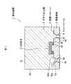
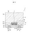
図1から図8は本発明の一実施形態を示し、図1は発光装置の概略縦断面図である。尚、各図においては、各部の構成を明確にするために実寸と異なるサイズで各部を示している。 1 to 8 show an embodiment of the present invention, and FIG. 1 is a schematic longitudinal sectional view of a light emitting device. In each drawing, each part is shown in a size different from the actual size in order to clarify the configuration of each part.
図1に示すように、この発光装置1は、フリップチップ型のGaN系半導体材料からなるLED素子2と、LED素子2を搭載する搭載基板3と、搭載基板3に形成される回路パターン4と、LED素子2を封止するとともに搭載基板3と接着される無機封止部としてのガラス封止部5とを有する。また、LED素子2と搭載基板3との間には、ガラスがまわりこまない中空部が形成されている。 As shown in FIG. 1, the
搭載基板3は、表面と裏面を連通するスルーホール6が形成される。本実施形態においては、アノード側とカソード側にそれぞれスルーホール6が配置され、各スルーホール6は、表面側に形成される縮径部6aと、裏面側に形成される拡径部6bと、を有する。縮径部6aは、スルーホール6における搭載基板3の表面側端部から厚さ方向中央まで形成され、裏面側へ向かって径が窄まるよう形成される。拡径部6bは、スルーホール6における搭載基板3の裏面側端部から厚さ方向中央まで形成され、裏面側へ向かって径が拡がるよう形成される。縮径部6aと拡径部6bは、それぞれ、厚さ方向について一定の割合で窄む、あるいは拡がって形成されている。 The
回路パターン4は、搭載基板3のスルーホール6の内面に形成される内面パターン41と、搭載基板3の表面に形成されLED素子2と電気的に接続される表面パターン42と、搭載基板3の裏面に形成され外部端子と接続可能な裏面パターン43と、を連続的に有している。回路パターン4は、例えば、W層、Ni層及びAu層の3層構造とすることができる。表面パターン42は、スルーホール6の表面側端部の周囲に形成された円形部42aと、円形部42aから基板中央側の発光素子2の搭載部44まで延びる接続部42bと、を有している。また、裏面パターン43は、スルーホール6の裏面側端部の周囲にて円形に形成されている。尚、内面パターン41は、スルーホール6の内面に全面的に形成されている。 The
図2は発光装置の概略平面図である。
搭載基板3は、アルミナ(Al2O3)の多結晶焼結材料からなり、厚さ0.25mmで1.0mm角に形成されており、熱膨張率αが7×10⁻⁶/℃である。また、LED素子2は、厚さ100μmで346μm角に形成されており、熱膨張率は7×10−6/℃である。ここで、LED素子2のGaN層の熱膨張率は5×10−6/℃であるが、大部分を占めるサファイアからなる成長基板の熱膨張率が7×10−6/℃であるため、LED素子2本体の熱膨張率は成長基板の熱膨張率と同等となっている。各スルーホール6は、搭載基板3の中央に搭載されたLED素子2を、平面視にて挟むよう配置される。本実施形態においては、2つのスルーホール6が、搭載基板3の一辺と平行な方向(対辺方向)において、LED素子2を挟むよう配置されている。FIG. 2 is a schematic plan view of the light emitting device.
The mounting
図3は、LED素子の模式縦断面図である。
発光素子としてのLED素子2は、図3に示すように、サファイア(Al2O3)からなる成長基板20の表面に、III族窒化物系半導体をエピタキシャル成長させることにより、バッファ層21と、n型層22と、MQW層23と、p型層24とがこの順で形成されている。このLED素子2は、700℃以上でエピタキシャル成長され、その耐熱温度は600℃以上であり、後述する低融点のガラスを用いた封止加工における加工温度に対して安定である。また、LED素子2は、p型層24の表面に設けられるp側電極25と、p側電極25上に形成されるp側パッド電極26と、を有するとともに、p型層24からn型層22にわたって一部をエッチングすることにより露出したn型層22に形成されるn側電極27を有する。p側パッド電極26とn側電極27には、それぞれAuバンプ28が形成される。FIG. 3 is a schematic longitudinal sectional view of the LED element.
As shown in FIG. 3, the
p側電極25は、例えば銀(Ag)からなり、発光層としてのMQW層23から発せられる光を成長基板20の方向に反射する光反射層として機能する。尚、p側電極25の材質は適宜変更が可能である。本実施形態においては、p側電極25上には2点のp側パッド電極26が形成され、各p側パッド電極26にAuバンプ28が形成される。尚、p側パッド電極26は例えば3点であってもよく、p側電極25上に形成するp側パッド電極26の個数は適宜変更が可能である。 The p-
n側電極27は、同一エリアにコンタクト層とパッド層とが形成されている。図2に示すように、n側電極27は、Al層27aと、このAl層27aを覆う薄膜状のNi層27bと、Ni層27bの表面を覆うAu層27cによって形成されている。尚、n側電極27の材質は適宜変更が可能である。本実施形態においては、平面視にて、n側電極27がLED素子2の隅部に形成され、p側電極25がn側電極27の形成領域を除いて、ほぼ全面的に形成されている。 In the n-side electrode 27, a contact layer and a pad layer are formed in the same area. As shown in FIG. 2, the n-side electrode 27 is formed of an
ガラス封止部5は、ZnO−B2O3−SiO2系のガラスからなる。尚、ガラスの組成はこれに限定されるものではなく、例えば、ガラスは、高屈折率とするためNb2O5を含んでもよいし、低融点化のためにNa2O、Li2O等を含有していてもよい。さらに、任意成分としてZrO2、TiO2等を含んでいてもよい。このガラスは、ガラス転移温度(Tg)が490℃で、屈伏点(At)が520℃であり、LED素子2の発光層(本実施形態ではMQW層23)におけるエピタキシャル成長時の形成温度よりも、ガラス転移温度(Tg)が十分に低くなっている。本実施形態においては、発光層のエピタキシャル成長温度よりも、ガラス転移温度(Tg)が200℃以上低くなっている。また、ガラスの100℃〜300℃における熱膨張率(α)は6×10⁻⁶/℃である。熱膨張率(α)は、ガラス転移温度(Tg)を超えるとこれより大きな数値となる。これにより、ガラスは約600℃で搭載基板3と接着し、ホットプレス加工が可能となっている。また、ガラス封止部5のガラスの屈折率は1.7である。
また、ガラスの組成は、ガラス転移温度(Tg)がLED素子2の耐熱温度よりも低く、熱膨張率(α)が搭載基板3と同等であれば任意である。ガラス転移温度が比較的低く、熱膨張率が比較的小さいガラスとしては、例えば、ZnO−SiO2−R2O系(RはLi、Na、K等のI族の元素から選ばれる少なくとも1種)のガラス、リン酸系のガラス及び鉛ガラスが挙げられる。これらのガラスでは、ZnO−SiO2−R2O系のガラスが、リン酸系のガラスに比して耐湿性が良好で、鉛ガラスのように環境的な問題が生じることがないので好適である。The glass composition is arbitrary as long as the glass transition temperature (Tg) is lower than the heat resistance temperature of the
ここで、本実施形態において、LED素子2の封止に用いられるガラスは、加熱により軟化状態として成形したガラスであり、ゾルゲル法により成形されるガラスと異なる。ゾルゲルガラスでは成形時の体積変化が大きいのでクラックが生じやすくガラスによる厚膜を形成することが困難であるところ、本実施形態のように熱により軟化させて搭載基板3に融着させるガラスはこの問題点を回避することができる。また、ゾルゲルガラスでは細孔を生じるので気密性を損なうことがあるが、本実施形態のガラスはこの問題点を生じることもなく、LED素子2の封止を的確に行うことができる。 Here, in this embodiment, the glass used for sealing the
また、本実施形態のガラスは、一般に、樹脂において高粘度といわれるレベルより、桁違いに高い粘度で加工される。さらに、ガラスの場合には、屈伏点を数十℃超えても粘度が一般の樹脂封止レベルまで低くはならない。また、一般の樹脂成型時レベルの粘度にしようとすると、LED素子の結晶成長温度を超える温度を要するもの、あるいは金型に付着するものとなり、封止・成形加工が困難になる。このため、104ポアズ以上109ポアズ以下で加工することが好ましい。In addition, the glass of this embodiment is generally processed with a viscosity that is orders of magnitude higher than the level of high viscosity in the resin. Furthermore, in the case of glass, the viscosity does not decrease to a general resin sealing level even if the yield point exceeds several tens of degrees Celsius. Further, if the viscosity is set to a level at the time of general resin molding, it requires a temperature exceeding the crystal growth temperature of the LED element or adheres to the mold, and sealing / molding processing becomes difficult. For this reason, it is preferable to process at 104 poise or more and 109 poise or less.
図1に示すように、ガラス封止部5は、発光素子2及び搭載基板3を全面的に覆い、厚さが0.5mmとなっている。ガラス封止部5は、搭載基板3と平行な上面5aと、上面5aの外縁から下方へ延び搭載基板3と垂直な側面5bと、を有している。さらに、ガラス封止部5は、搭載基板3のスルーホール6の内部へ進入した係合部5cを有している。係合部5cは、縮径部6aを超えて拡径部6bの途中まで形成されている。係合部5cは、スルーホール6の裏面側端部までは形成されていない。 As shown in FIG. 1, the
以上のように構成された発光装置1では、回路パターン4を通じてLED素子2に電圧が印加されると、LED素子2から青色光が発せられる。LED素子2から発せられた青色光は、ガラス封止部5の上面5a又は側面5bを通じて外部へ放射される。 In the
この発光装置1は、以下の工程を経て製造される。
まず、ガラス成分の酸化物粉末を1200℃に加熱し、溶融状態で撹拌する。そして、ガラスを固化した後、ガラス封止部5の厚さに対応するようスライスして封止前ガラス11を板状に加工する(板状加工工程)。この後、封止前ガラス11に、後述するように、各LED素子2に対応する凹部11aを形成する。The
First, a glass component oxide powder is heated to 1200 ° C. and stirred in a molten state. And after solidifying glass, it slices so that it may correspond to the thickness of the
一方、平板状の搭載基板3に、サンドブラスト加工、レーザ加工等によりスルーホール6を形成する(ホール形成工程)。サンドブラスト加工の場合、研磨材の飛散角度を変化させることにより縮径部6a及び拡径部6bを形成することができるし、レーザ加工の場合、レーザーの集光角度を変化させることにより縮径部6a及び拡径部6bを形成することができる。 On the other hand, the through
スルーホール6が形成された後、搭載基板3に回路パターン4を形成する(パターン形成工程)。パターン形成工程では、内面パターン41と、表面パターン42と、裏面パターン43と、を連続的に形成する。例えば、回路パターン4は、金属ペーストをスクリーン印刷し、搭載基板3を所定温度(例えば1000℃以上)で熱処理することにより当該金属を搭載基板3に焼き付けた後、当該金属に他の金属のめっきを施すことにより形成することができる。また、搭載基板3に金属を蒸着して他の金属のめっきを施したり、金属を貼り付けた後に当該金属を所定形状にエッチングして他の金属のめっきを施してもよい。 After the through
この後、複数のLED素子2を縦及び横について等間隔で搭載基板3の搭載部44に搭載する(搭載工程)。具体的には、搭載基板3の回路パターン4の表面パターン41に複数のLED素子2を各Auバンプ28によって電気的に接合する。本実施形態においては、p側2点、n側1点の合計3点のバンプ接合が施される。また、搭載基板3は、各LED素子2の搭載領域の外側に形成される面積増大部としての溝部31(図4参照)を有している。本実施形態においては、溝部31が二重に形成されている。 Thereafter, the plurality of
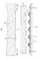
そして、図4に示すように、各LED素子2が搭載された搭載基板3を下金型91にセットし、上金型92を搭載基板3の搭載面と対向して配置し、搭載基板3と上金型92の間に各LED素子2の搭載領域が覆われるように封止前ガラス11を配置する(プレス準備工程)。尚、このとき、封止前ガラス11は、各LED素子2と接触していてもよいし、離隔していてもよい。下金型91及び上金型92にはそれぞれヒータが配置され、各金型91,92で独立して温度調整される。上金型92は、各LED素子2の上方の封止前ガラスと接触する平坦面92aと、平坦面92aの外縁側に形成され下方へ突出形成される流出抑制部92bと、を有している。本実施形態においては、流出抑制部92bは、先端に向かって細くなるように、各LED素子2側の面が傾斜して形成された突出部である。上金型92は、例えば、ステンレス、タングステンカーバイド等からなる。本実施形態においては、上金型92の流出抑制部92bは、底面視にて四角のリング状に形成されている。 Then, as shown in FIG. 4, the mounting
本実施形態においては、封止前ガラス11は板状に形成され、搭載基板3側に各LED素子2に対応して凹部11aが形成されている。この後、下金型91及び上金型92を加圧し、窒素雰囲気中で加熱によって軟化したガラス材のホットプレス加工を行う(ホットプレス工程)。図5に示すように、ホットプレス工程では、プレスによりガラス材を搭載基板3の表面に接合してLED素子2を封止しつつ、ガラス材をスルーホール6の少なくとも拡径部6bまで進入させる。ここで、封止前ガラス11と搭載基板3の間の気体は、スルーホール6を通じて外部へ排出される。図5は、ガラス材の封止加工時の状態を示す模式説明図である。本実施形態においては、軟化したガラス材は拡径部6bの途中まで入り込んで、搭載基板3の裏面側までは到達しない。尚、ガラス材が搭載基板3の裏面側まで到達しても、LED素子2の封止自体の問題はないが、ガラス材が下金型91と接着するおそれがある。このときの加工条件は、ガラスの温度、圧力、スルーホール径等に応じて任意に変更することができるが、一例をあげるとすれば、例えば、ガラスの温度を600℃とし、ガラスの圧力を25kgf/cm2とし、スルーホール径を0.1mmとすることができる。また、封止前ガラス11は、搭載基板3への配置前に加熱されていてもよいし、配置後に加熱されるようにしてもよく、プレス時に搭載基板3の表面上に加熱により軟化した状態で配置されていればよい。In the present embodiment, the
ここで、ホットプレス加工は、各金型91,92をはじめとする装置各部の酸化を防止する場合、各部材に対して不活性な雰囲気中で行えばよく、窒素雰囲気の他に例えば真空中で行うようにしてもよい。尚、各金型91,92をはじめとする装置各部の酸化が問題とならない場合、空気中でホットプレス加工を行ってもよい。 Here, in order to prevent oxidation of each part of the apparatus including the
図5に示すように、封止前ガラス11の上面に上金型92の平坦面92aが全面的に接触し、加圧により軟化した封止前ガラス11が横方向へ流出するところ、上金型92の流出抑制部92bが封止前ガラス11の流出を抑制することにより、流出抑制部92bの内側ではガラスの圧力をほぼ一定にすることができる。プレス加工時、軟化したガラス材は高粘度の流体として振る舞い、上金型92と搭載基板3により圧縮され、上金型92と搭載基板3との間隙が中央側と外縁側にわたって一定であるならば、外縁側と中央側とで圧力差が生じやすい状態となる。しかしながら、流出抑制部92bを設けることにより、ガラス材の流出方向を絞りつつ、内側にキャビティを形成することによって、各LED素子2付近のガラスの圧力をほぼ一定とすることができるのである。すなわち、本実施形態の製造方法は、高粘度のガラスを用いてホットプレス加工により各LED素子2を封止する際の新規な課題を解決したものである。尚、本実施形態においては、流出抑制部92bの先端が搭載基板3と接触していないことから、余分なガラス材は流出抑制部92bから外側へ流出する。これにより、キャビティ内のガラス材の過度の圧力上昇を回避することができる。 As shown in FIG. 5, the
図5に示すように、封止前ガラス11の上面は、平坦面92aにより全体にわたって平坦に形成される。また、軟化したガラス材は、搭載基板3の各溝部31に入り込んで、各溝部31の表面と接合する。ここで、各溝部31は、流出抑制部92bの外側に配置されている。 As shown in FIG. 5, the upper surface of the
以上の工程で、複数の発光装置1が縦方向及び横方向に連結された状態の図6に示すような中間体12が作製される。この後、ガラス封止部5と一体化された搭載基板3をダイシング装置にセットして、ダイシングブレードによって、ガラス封止部5及び搭載基板3を各LED素子2ごとに分割するようダイシングして発光装置1が完成する(分割工程)。 Through the above steps, the
以上の発光装置1の製造方法によれば、ホットプレス時にガラス材料を拡径部6bまで進入させているので、ガラス材料が硬化した後に当該進入した部分が係合部5cとなり、ガラス封止部5が搭載基板3に強固に固定される。これにより、ガラス封止部5に搭載基板3から剥離する方向に力が加わったとしても、係合部5cがスルーホール6に引っ掛かるので、ガラス封止部5が搭載基板3から離脱することはない。従って、例えば樹脂封止の発光装置で使用不能であった高圧下等の過酷な環境での使用も可能となるし、信頼性が格段に向上する。 According to the manufacturing method of the
また、本実施形態によれば、ガラス材が硬化した後にガラス封止部5を分割していることから、分割時にガラス封止部5に負荷が加わることとなる。このとき、ガラス封止部5に係合部5cが形成され、搭載基板3に対して強固に固定されていることから、分割時におけるガラスの剥離を抑制して歩留まりを向上させることができる。また、従来よりも剥離し難くなることから、例えば、ダイシング時のダイシングブレードの歯を粗くしたり回転速度を上げることができ、分割工程に要する時間を短縮して、発光装置1の生産性を向上させることができる。 Moreover, according to this embodiment, since the
また、スルーホール6を各発光装置1に形成したことにより、ホットプレス時に各発光装置1の各LED素子2をカバーする板状のガラス材と搭載基板3との間の気体を外部へ逃がすことができ、ガラス封止部5と搭載基板3との間に残留気体層が生じることを防止して接合状態を良好とし、これによっても強度を向上させることができる。また、減圧雰囲気で封止を行ったり、ガラス材と搭載基板3の間の気体を逃がすための機構等を設ける必要がなく、製造コストの低減を図ることができる。
尚、発明者らの実験で、0.34mm角のLED素子が1.1mmのピッチで、100pcs(10×10)以上配列された搭載基板への板ガラス接合においても、ガラス材と搭載基板の接合面に残留気体層を生じさせることなく、良好な接合状態が実現されることが確認されている。この実験での、搭載基板の表面の面積は、ダイシングによる切りしろを含めて、123.21mm2(11.1mm×11.1mm)であった。このように、一回のガラス封止工程で100pcs以上の発光装置の封止が可能となる。さらに、0.34mm角のLED素子が1.1mmピッチで784pcs(28×28)で配列された搭載基板への板ガラス接合においても、ガラス材と搭載基板との間に残留気体層が生じないことも確認されている。
ここで、ガラス材とアルミナ製の搭載基板3では、アンカ−効果と酸素化合物を介しての化学結合がされている。そして、搭載基板3の素子搭載面(表面)には、回路パタ-ン4を取り囲むようにガラス材と搭載基板3の接合面が形成され、当該接合面に残留気体層が生じないようにすることができ、接合部の気密性に優れている。さらにまた、回路パタ-ン4の腐食も防ぐことができる。Further, by forming the through
In addition, in the experiments by the inventors, even in the plate glass bonding to a mounting substrate in which 0.34 mm square LED elements are arranged at a pitch of 1.1 mm and more than 100 pcs (10 × 10), the bonding of the glass material and the mounting substrate is also performed. It has been confirmed that a good bonded state is realized without causing a residual gas layer on the surface. The area of the surface of the mounting substrate in this experiment was 123.21 mm2 (11.1 mm × 11.1 mm) including the margin for dicing. In this manner, a light emitting device of 100 pcs or more can be sealed in a single glass sealing step. Furthermore, a residual gas layer is not generated between the glass material and the mounting substrate even in the plate glass bonding to the mounting substrate in which 0.34 mm square LED elements are arranged at 784 pcs (28 × 28) at a pitch of 1.1 mm. Has also been confirmed.
Here, in the glass material and the mounting
さらに、仮に、中間体12の外縁側にて、ガラス封止部5と搭載基板3との間に部分的に剥離が生じたとしても、各スルーホール6には軟化したガラス材が進入しているため、分割工程にてガラス封止部5の全体が一気に搭載基板3から剥離するようなことはなく、剥離の影響を剥離箇所周辺の発光装置1にとどめることができ、これによっても歩留まりが向上する。 Furthermore, even if partial peeling occurs between the
また、ガラス封止時に、搭載領域上のガラス材の圧力がほぼ一定となるので、搭載基板3の外縁側でのガラス材の圧力を増大させることができ、ガラス材と搭載基板3との接合強度が増大し、ガラス材の搭載基板3からの剥離を抑制することができる。さらに、ガラス材が搭載基板3の各溝部31へ入り込むので、ダイシングの際、ダイシングブレードがガラス端部をめくり上げてガラス材が搭載基板3から剥がれることを抑制できる。 In addition, since the pressure of the glass material on the mounting area becomes almost constant at the time of glass sealing, the pressure of the glass material on the outer edge side of the mounting
また、搭載領域内の各LED素子2に加わる圧力を一定とすることができる。これにより、各LED素子2の封止条件を均一とし、各LED素子2の特性をより均一に近づけることができる。特に本実施形態のように、各LED素子2がバンプ28等を介して搭載基板3に実装されている場合、各LED素子2と搭載基板3との間に隙間が存在する。そして、ガラスの圧力及び流れ方向によって当該隙間へのガラスの回り込み状態が異なり、この回り込み状態がLED素子2の特性に大きく影響するところ、回り込み状態を均一に近づけて各LED素子2の特性ばらつきを抑制することができる。 Further, the pressure applied to each
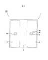
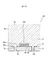
図7は、光源装置の概略断面図である。
図7に示すように、発光装置1は、実装基板7に実装して光源装置100として使用することができる。実装基板7は、金属からなるベース部71と、ベース部71上の絶縁層72と、絶縁層72上の回路パターン73と、を有する。発光装置1を実装基板7に実装するにあたり、発光装置1の搭載基板3の裏面におけるスルーホール6の周囲に形成されている裏面パターン43と、実装基板7の回路パターン73と、をはんだ8を介して接合する。はんだ8は、スルーホール6内に侵入した侵入部8aを有する。ベース部71は例えばアルミニウムからなり、絶縁層72は例えばエポキシ系等の樹脂、酸化アルミニウム等のセラミックからなり、回路パターン73は例えばNi/Auからなる。尚、実装基板7として、金属ベースの基板の他に、ポリイミドや液晶ポリマーで形成されるフレキシブル基板、ガラスエポキシ基板等の他の基板を用いてもよい。FIG. 7 is a schematic cross-sectional view of the light source device.
As shown in FIG. 7, the
図8は、図7のA−A断面図である。
図8に示すように、はんだ8は、スルーホール6を包囲する裏面パターン43と全面的に接合している。はんだ8は、スルーホール6を完全に塞ぐよう形成され、スルーホール6内が外気に直接的に曝されないよう構成されている。これにより、スルーホール6から発光装置1の内部への水分等の浸入を抑制することができ、発光装置1に優れた耐候性を発揮させることができる。尚、ガラスやセラミックの透湿性は、樹脂部材と比較すると極めて小さく、樹脂と比較すればゼロに等しいとみなすことができる。本実施形態においては、係合部5cがスルーホール6の裏面側まで到達しておらず、スルーホール6にはんだ8を受容するスペースがあるため、はんだ8に侵入部8aを形成することができ、平面だけでなく立体的に接合部を形成することができるので、はんだ接合の強度を増すことができる。また、外力を受けにくいオープンホール内へはんだ8が入ることで、経年劣化での接合不良も生じにくくなる。尚、はんだ8に限らず、銀ペースト等の金属粒子を用いた導電性接着剤を用いても、同様の効果を得ることができる。FIG. 8 is a cross-sectional view taken along the line AA of FIG.
As shown in FIG. 8, the
尚、前記実施形態においては、流出抑制部92bを上金型92に設けたものを示したが、搭載基板3に流出抑制部を設けてもよいし、上金型92と搭載基板3ともに流出抑制部を設けない構成としてもよいことは勿論である。また、搭載基板3に溝部31を形成したものを示したが、搭載基板3の表面積を増大させるものであれば、凹状、凸状等の他の形状としてもよいし、溝部31を形成しない構成であってもよい。また、封止前ガラス11は、各LED素子2に対応した凹部11が形成されていない平坦なガラスであってもよい。 In the above-described embodiment, the
また、前記実施形態においては、2つのスルーホール6を搭載基板3の対辺方向においてLED素子2を挟み込むよう配置したものを示したが、例えば図9に示すように搭載基板3の対角方向においてLED素子2を挟み込むよう配置してもよい。また、スルーホール6の径について、0.1mmを例示したが、ガラスの粘度、圧力により適宜変更することができ、拡径部6bへのガラスの進入がありLED素子2が搭載されていない搭載基板3の裏面にまで至らないものであれば、例えば径を0.05m以上0.5mm以下とすることができる。 In the above embodiment, the two through
また、前記実施形態においては、1つの発光装置1に1つのLED素子2が搭載されるものを示したが、例えば図10及び図11に示すように、1つの発光装置に複数のLED素子2が搭載されるものであってもよい。図10の発光装置1は、3つのLED素子2が直線状に配置されており、2つのスルーホール6がその直線上で各LED素子2を挟むよう配置されている。尚、隣接するLED素子2は、表面パターン42の連接部42cにより接続され、各LED素子2は電気的に直列となっている。図11の発光装置1は、9つのLED素子2が縦3列、横3列に配置されており、2つのスルーホール6が各LED素子2の搭載領域を対角方向にて挟むよう配置されている。尚、各LED素子2は、電気的に直列となっている。 Moreover, in the said embodiment, although the one
また、前記実施形態においては、スルーホール6が縮径部6aと拡径部6bとを有するものを示したが、例えば図12に示すように、スルーホール16が表面側の小径部16aと裏面側の大径部16bとを有するようにしてもよい。小径部16a及び大径部16bは、搭載基板3の厚さ方向について同一径に形成され、小径部16aと大径部16bの境界部16cが拡径部をなしている。そして、ガラス封止部5のガラスが拡径部を超えてスルーホール内に進入して係合部5cをなしている。この発光装置1では、搭載基板3として多層セラミック基板が用いられ、小径部16aが第1層3aに形成され、大径部16bが第2層3bに形成されており、小径部16a及び大径部16bは径の異なる抜き型でのパンチングにより成形される。 In the above embodiment, the through
ここで、図12の発光装置1では第1層3a及び第2層3bが同じ厚さに形成されているが、例えば図13に示すように、表面側の第1層3aの厚さを裏面側の第2層3bの厚さより薄くしてもよい。この場合、境界部16cから搭載基板3の裏面までの距離を大きくとることができるとともに、スルーホール6内の空間が大きくなるので、ガラスのホットプレス加工時に、スルーホール6内へ進入したガラスが搭載基板3の裏面まで比較的到達し難くでき、実用に際して有利である。 Here, in the
さらに、スルーホール6の縮径部6aを省略し、例えば図14に示すように、拡径部6bのみの構成としてもよい。尚、縮径部6aの厚さを比較的薄くし、拡径部6bの厚さを比較的厚くした構造とすることもできる。図14の発光装置1では、スルーホール6の内面の傾斜角が一定であるので、搭載基板3に負荷が加わった際に応力が分散されやすく割れ、欠け等が生じ難いし、スルーホール6内のガラスの係合部5cを比較的滑らかに形成することができる。また、この場合も、ガラスのホットプレス加工時に、スルーホール6内へ進入したガラスが搭載基板3の裏面まで比較的到達し難くできる。 Further, the reduced
また、前記実施形態においては、ガラス封止部5の上面5aが搭載基板3と平行に形成されたものを示したが、例えば図15に示すように、ガラス封止部5の上面5dが湾曲形成されたものであってもよい。図15の発光装置1では、ガラス封止部5の上面5dが上方へ向かって凸に形成されているが、上方へ向かって凹に形成されていたり、例えばフレネルレンズのように複数の湾曲面が形成されていてもよい。 Moreover, in the said embodiment, although the
また、例えば図16及び図17に示すように、LED素子2から発せられる光の波長を変換する蛍光体9aを含有させることもできる。蛍光体9aとして、例えば、YAG(Yttrium Aluminum Garnet)蛍光体、珪酸塩蛍光体や、YAGと珪酸塩蛍光体を所定の割合で混合したもの等を用いることができる。この場合、LED素子2から発せられた青色光の一部はガラス封止部5内の蛍光体9aにより黄色光に変換され、他部は波長変換されることなくガラス封止部5から外部へ放射される。これにより、ガラス封止部5から放射される光は、黄色領域と青色領域とにピーク波長を有することとなり、この結果、装置外部へは白色光が放射される。また、紫外光を発するLED素子と、青色蛍光体、緑色蛍光体、赤色蛍光体の組合せにより白色光を得るようにしてもよい。 For example, as shown in FIG.16 and FIG.17, the
図16の発光装置1では、LED素子2を蛍光体9aが含有された無機ペースト9で被覆してから、LED素子2をガラス材により封止している。無機ペースト9としては、例えば、SiO2系、Al2O3系、TiO2系のアルコキシドやゾルゲルガラスを用いることができる。尚、LED素子2の基板としてGaN基板を用いた場合、無機ペースト9をGaNよりも屈折率の高いTiO2系のアルコキシドとすると、LED素子2からの光取り出し効率を向上させつつ、蛍光体9aの波長変換を効率良く行うことができる。また、この場合、LED素子2と搭載基板3との間に中空部がなくなることから、ホットプレス時にガラス封止部5と搭載基板3との間に残留気体層がより生じやすくなるが、オープンなスルーホール6を形成したことにより、接合状態を良好に保つことができる。尚、オープンなスルーホール6は、Auバンプ28のようなスタッドバンプを用いずに、共晶材料、導電性接着剤等を用いてLED素子2を実装したり、あるいはLED素子2を直接に実装すること等により、LED素子2と搭載基板3との間の中空部の体積が小さくなった際にも有効である。In the
図17の発光装置1では、ガラス封止部5のガラス材に蛍光体9aを分散させている。図17に示すように、この発光装置1は、ガラス封止部5に分散された拡散粒子9bを有している。拡散粒子9bとしては、例えばジルコニア粒子、アルミナ粒子、シリカ粒子等を用いることができる。拡散粒子の材質は任意であるが、光の透過性の観点からは白色の材質が好ましく、ガラス加工時の安定性の観点からは融点が加工時の温度より高いことが好ましい。 In the
また、前記実施形態においては、スルーホール6が拡径部6bを有するものを示したが、例えば図18及び図20に示すように、スルーホール106の径が一定であってもよい。図18の発光装置101では、スルーホール106は、断面一定のストレート形状に形成されている。これによっても、ホットプレス時に各発光装置1の各LED素子2をカバーする板状のガラス材と搭載基板3との間の気体を外部へ逃がすことができ、ガラス封止部5と搭載基板3との間に残留気体層が生じることを防止して接合状態を良好として強度を向上させることができる。また、減圧雰囲気で封止を行ったり、ガラス材と搭載基板3の間の気体を逃がすための機構等を設ける必要がなく、製造コストの低減を図ることができる。 Moreover, in the said embodiment, although the through
また、ガラス封止時に、搭載領域上のガラス材の圧力がほぼ一定となるので、搭載基板3の外縁側でのガラス材の圧力を増大させることができ、ガラス材と搭載基板3との接合強度が増大し、ガラス材の搭載基板3からの剥離を抑制することができる。さらに、搭載領域内の各LED素子2に加わる圧力を一定とすることができる。これにより、各LED素子2の封止条件を均一とし、各LED素子2の特性をより均一に近づけることができる。この際、例えば図5に示した上金型92では、LED素子2が実装されていない封止前ガラス11の周囲部を先に塞いでいるため、搭載基板3に複数実装されている各LED素子2の間の気体層が残留し易いが、搭載基板3のスルーホール6からこの気体を逃がし、ガラスと搭載基板3との間の気体層をなくし、良好な接合を得ることができる。尚、図5に示した上金型92以外に、封止前ガラス11の周囲に枠部材を設ける、搭載基板3の端部側に凸状の段差を設ける等の手段により、ガラス材の流出抑制を行う場合でも同様の効果を得ることができる。 In addition, since the pressure of the glass material on the mounting area becomes almost constant at the time of glass sealing, the pressure of the glass material on the outer edge side of the mounting
また、発光装置101には、図19に示すLED素子102が用いられている。LED素子102は、前述のLED素子2のようなAuバンプ28に代えて、p側パッド電極26を形成せずに、導電性接着剤128をp側電極25の下に充填して回路パターン4と電気的に接続している。導電性接着剤128の厚さは、例えば50μm以下である。また、導電性接着剤128の面積は、平面視にて、例えば、LED素子102の50%以上である。このように、LED素子102と搭載基板3との間の中空部が小さい場合には、ホットプレス時にガラス封止部5と搭載基板3との間に残留気体層がより生じやすくなるが、オープンなスルーホール106を形成したことにより、接合状態を良好に保つことができる。尚、導電性接着剤128の他に、共晶材料を用いてLED素子102を実装したり、あるいはLED素子102を直接に実装してもよい。 In addition, the
例えば、この発光装置101は、例えば、搭載基板3をなすグリーンシートにプレス型でスルーホール106を形成しておく。そして、回路パターン4に対応する領域にWペーストを塗布した後にグリーンシートを焼成し、Niめっきと、Au、Ag等のめっきを施しセラミックの搭載基板3とする。或いは、スルーホール106が形成されたグリーンシートをそのまま焼成した後、Agペーストを塗布して焼成して、回路パターン4が形成された搭載基板3を作製することができる。 For example, in the
また、図20に示すように、発光装置201は、回路パターン4がスルーホール106の下側を塞ぐ閉塞パターン45を有していてもよい。閉塞パターン54は、例えば、スルーホール106を形成した後にAgペーストからなる回路パターン4を形成する際に、初回に内面パターン41及び表面パターン42を形成し、2回目にスルーホール106の径が小さくなったところへ、裏面パターン43とともに形成することができる。 In addition, as illustrated in FIG. 20, the
また、前記実施形態においては、LED素子2としてGaN系半導体材料からなるものを用いた発光装置1を説明したが、LED素子はGaN系のLED素子2に限定されず、例えばZnSe系やSiC系のように他の半導体材料からなる発光素子であってもよい。また、LED素子2の発光波長も任意であり、LED素子2は緑色光、黄色光、橙色光、赤色光等を発するものであってもよい。 Moreover, in the said embodiment, although the light-emitting
また、前記実施形態のガラス封止部5は耐候性に優れているものの、装置の使用条件等によって結露が生じた場合には、ガラス封止部5が変質するおそれがある。これに対しては、結露が生じない装置構成とすることが望ましいが、ガラス封止部5の表面にシリコン樹脂コートなどを施すことで、高温状態での結露によるガラスの変質を防止することもできる。さらに、ガラス封止部5の表面に施すコーティング材としては、耐湿だけでなく、耐酸、耐アルカリ性を有するものとして、例えばSiO2系、Al2O3系等のような無機材料が好ましい。Moreover, although the
さらに、前記実施形態においては、上金型92と下金型91により搭載基板3及びガラス封止部5に圧力を加えるものを示したが、下金型91を固定部材として上金型92のみによりガラスの封止加工を行うことも可能である。 Furthermore, in the above-described embodiment, the
また、前記実施形態のガラス封止部5について、B2O3−SiO2−Li2O−Na2O−ZnO−Nb2O5系のガラスを用いることもできるし、当該ガラスのZnO組成の一部をBi2O3とし、ガラスの屈折率をさらに高くしてもよい。ガラスの屈折率は、1.8であることが好ましい。そして、屈折率が1.8のガラスを用いる場合、基板の屈折率(nd)が1.8以上である発光素子を用いることが、発光素子からの光の取り出し効率を向上させて発光効率の向上を図ることができ好ましい。基板の屈折率が1.8以上である発光素子としては、例えば、Ga2O3基板、GaN基板、SiC基板等の上にGaN系半導体が形成された発光素子がある。また、セットされるガラス材は、バルク状のものに限らず、粉体を固めたもの等であってもよい。ガラス材は、加熱されて高粘度状態となってしまえば、加工前の状態による差異は見られなくなる。Furthermore, the
また、前記実施形態においては、搭載基板3がアルミナ(Al2O3)からなるものを示したが、アルミナ以外のセラミックから構成するようにしてもよい。ここで、アルミナより熱伝導性に優れる高熱伝導性材料からなるセラミック基板として、例えば、BeO(熱膨張率α:7.6×10⁻⁶/℃、熱伝導率:250W/(m・k))を用いても良い。このBeOからなる基板においても封止前ガラスにより良好な封止性を得ることができる。Further, in the above embodiment shows what is mounting
さらに、他の高熱伝導性基板として、例えばW−Cu基板を用いても良い。W−Cu基板としては、W90−Cu10基板(熱膨張率α:6.5×10⁻⁶/℃、熱伝導率:180W/(m・k))、W85−Cu15基板(熱膨張率α:7.2×10−6/℃、熱伝導率:190W/(m・k))を用いることにより、ガラス封止部との良好な接合強度を確保しながら高い熱伝導性を付与することができ、LEDの大光量化、高出力化に余裕をもって対応することが可能になる。Furthermore, for example, a W—Cu substrate may be used as another highly heat conductive substrate. As a W-Cu substrate, a W90-Cu10 substrate (thermal expansion coefficient α: 6.5 × 10⁻⁶ / ° C., thermal conductivity: 180 W / (m · k)), a W85-Cu15 substrate (thermal expansion coefficient α: By using 7.2 × 10⁻⁶ / ° C. and thermal conductivity: 190 W / (m · k)), it is possible to impart high thermal conductivity while ensuring good bonding strength with the glass sealing portion. Therefore, it is possible to cope with an increase in the amount of light and output of the LED with a margin.
また、前記実施形態においては、発光素子としてLED素子を用いた発光装置を説明したが、発光素子はLED素子に限定されるものではない。さらに、下金型91は必ずしも必要ではなく、金型を上金型92のみとしてもよいし、その他、具体的な細部構造等についても適宜に変更可能であることは勿論である。 Moreover, in the said embodiment, although the light-emitting device using an LED element as a light emitting element was demonstrated, a light emitting element is not limited to an LED element. Further, the
1 発光装置
2 LED素子
3 搭載基板
3a 第1層
3b 第2層
4 回路パターン
5 ガラス封止部
5a 上面
5b 側面
5c 係合部
6 スルーホール
6a 縮径部
6b 拡径部
7 実装基板
8 はんだ
9 無機ペースト
9a 蛍光体
9b 拡散粒子
11 封止前ガラス
11a 凹部
12 中間体
16 スルーホール
16a 小径部
16b 大径部
16c 境界部
20 成長基板
21 バッファ層
22 n型層
23 MQW層
24 p型層
25 p側電極
26 p側パッド電極
27 n側電極
27a Al層
27b Ni層
27c Au層
28 Auバンプ
41 内面パターン
42 表面パターン
43 裏面パターン
44 搭載部
45 閉塞パターン
71 ベース部
72 絶縁層
73 回路パターン
91 下金型
92 上金型
92a 平坦面
92b 流出抑制部
100 光源装置
101 発光装置
106 スルーホール
201 発光装置DESCRIPTION OF
Claims (7)
Translated fromJapanese前記搭載基板の表面と裏面を連通するスルーホールを前記発光装置に形成するホール形成工程と、
前記搭載基板における前記スルーホールの内面と、前記搭載基板の表面における前記スルーホールの端部から前記発光素子の搭載部までと、前記搭載基板の裏面における前記スルーホールの周囲と、に連続的に回路パターンを形成するパターン形成工程と、
前記搭載基板の前記搭載部に前記発光素子を搭載する搭載工程と、
加熱により軟化した前記ガラスを前記搭載基板の表面上に配置し、プレス動作により前記ガラスを前記搭載基板の表面に接合して前記発光素子を封止しつつ、前記ガラスを前記発光装置に形成された前記スルーホールに進入させるホットプレス工程と、を含み、
前記ホットプレス工程は、前記ガラスと接触する接触面の外縁側に形成され、先端が前記搭載基板と接触しない流出抑制部を有した金型によって実行される前記プレス動作を含み、前記流出抑制部は、封止前の前記ガラスの外側への流出を抑制する発光装置の製造方法。A method of manufacturing a light emitting device in which a light emitting element on a surface of a mounting substrate is sealed withglass ,
A hole forming step of forming a through hole in the light emitting device to communicate the front surface and the back surface of the mounting substrate;
The inner surface of the through hole in the mounting substrate, the end of the through hole on the surface of the mounting substrate to the mounting portion of the light emitting element, and the periphery of the through hole on the back surface of the mounting substrate. A pattern forming step for forming a circuit pattern;
A mounting step of mounting the light emitting element on the mounting portion of the mounting substrate;
Theglass softened by heating is disposed on the surface of the mounting substrate, and theglass is formed on the light emitting device while the light emitting element is sealed by bonding theglass to the surface of the mounting substrate by a pressing operation. And a hot press step for entering the through hole,
The hot pressing step includes the pressing operation performed by a mold having an outflow suppression unit that is formed on an outer edge side of a contact surface that comes into contact with theglass and whose tip does not contact the mounting substrate, and the outflow suppression unit The manufacturing method of the light-emitting device which suppresses the outflow to the outer side of the saidglass before sealing.
前記ホットプレス工程にて、前記ガラスを前記発光装置に形成された前記スルーホールの前記拡径部まで進入させる請求項1に記載の発光装置の製造方法。The through hole formed in the light emitting device formed in the hole forming step has an enlarged diameter portion whose diameter is expanded toward the back surface side,
The manufacturing method of the light-emitting device according to claim 1, wherein in the hot pressing step, theglass ismade to enter the enlarged diameter portion of the through hole formed in the light-emitting device.
前記搭載基板の表面と裏面を連通するスルーホールと、
前記搭載基板における前記スルーホールの内面と、前記搭載基板の表面における前記スルーホールの端部から前記発光素子の搭載部までと、前記搭載基板の裏面における前記スルーホールの周囲と、に連続的に形成された回路パターンと、
前記搭載基板の表面上にて前記発光素子を封止し、前記スルーホールに進入しているガラス封止部と、を備え、
前記スルーホールは、裏面側へ向かって径が拡がる拡径部を有し、
前記ガラス封止部は、前記スルーホールの前記拡径部まで進入しているとともに前記搭載基板の裏面における前記スルーホールの端部にまで到達していないことにより、前記スルーホールの端部から内部にかけて、はんだを受容するスペースを提供する係合部を有する発光装置。A light emitting device in which a light emitting element on a surface of a mounting substrate is sealed withglass ,
A through hole communicating the front surface and the back surface of the mounting substrate;
The inner surface of the through hole in the mounting substrate, the end of the through hole on the surface of the mounting substrate to the mounting portion of the light emitting element, and the periphery of the through hole on the back surface of the mounting substrate. A formed circuit pattern;
Sealing the light emitting element on the surface of the mounting substrate, and including aglass sealing portion entering the through hole,
The through hole has an enlarged diameter part whose diameter is enlarged toward the back surface side,
The glass sealing portion has entered from the end portion of thethrough-hole to the inside of the through-hole by not reaching the end portion of the through-hole on the back surface of the mounting substrate while entering the enlarged-diameter portionof the through-hole. And a light emitting device havingan engaging portion thatprovides a space for receiving solder .
前記発光装置の前記搭載基板の裏面における前記スルーホールの周囲に形成されている前記回路パターンと、前記実装基板の回路パターンと、をはんだを介して又は直接的に接合する発光装置の実装方法。In mounting the light emitting device according to claim 5 on a mounting substrate,
A mounting method of a light emitting device, wherein the circuit pattern formed around the through hole on the back surface of the mounting substrate of the light emitting device and the circuit pattern of the mounting substrate are joined via solder or directly.
前記発光装置が実装される実装基板と、
前記発光装置の前記搭載基板の裏面における前記スルーホールの周囲に形成されている前記回路パターンと、前記実装基板の回路パターンとの間に介在し、前記スルーホールに侵入した侵入部を有するはんだと、を備えた光源装置。A light emitting device according to claim 5;
A mounting substrate on which the light emitting device is mounted;
A solder interposed between the circuit pattern formed around the through-hole on the back surface of the mounting substrate of the light-emitting device and the circuit pattern of the mounting substrate and having an intrusion portion that has entered the through-hole; A light source device.
Priority Applications (3)
| Application Number | Priority Date | Filing Date | Title |
|---|---|---|---|
| JP2010062514AJP5659519B2 (en) | 2009-11-19 | 2010-03-18 | Light emitting device, method for manufacturing light emitting device, method for mounting light emitting device, and light source device |
| CN201010539386.5ACN102097544B (en) | 2009-11-19 | 2010-11-03 | Light-emitting device, method of manufacturing the same, method of mounting the same and lighting device |
| US12/926,253US9653661B2 (en) | 2009-11-19 | 2010-11-04 | Light-emitting device, method of manufacturing the same, method of mounting the same and lighting device |
Applications Claiming Priority (3)
| Application Number | Priority Date | Filing Date | Title |
|---|---|---|---|
| JP2009264095 | 2009-11-19 | ||
| JP2009264095 | 2009-11-19 | ||
| JP2010062514AJP5659519B2 (en) | 2009-11-19 | 2010-03-18 | Light emitting device, method for manufacturing light emitting device, method for mounting light emitting device, and light source device |
Publications (2)
| Publication Number | Publication Date |
|---|---|
| JP2011129862A JP2011129862A (en) | 2011-06-30 |
| JP5659519B2true JP5659519B2 (en) | 2015-01-28 |
Family
ID=44010643
Family Applications (1)
| Application Number | Title | Priority Date | Filing Date |
|---|---|---|---|
| JP2010062514AActiveJP5659519B2 (en) | 2009-11-19 | 2010-03-18 | Light emitting device, method for manufacturing light emitting device, method for mounting light emitting device, and light source device |
Country Status (3)
| Country | Link |
|---|---|
| US (1) | US9653661B2 (en) |
| JP (1) | JP5659519B2 (en) |
| CN (1) | CN102097544B (en) |
Families Citing this family (35)
| Publication number | Priority date | Publication date | Assignee | Title |
|---|---|---|---|---|
| US9640737B2 (en) | 2011-01-31 | 2017-05-02 | Cree, Inc. | Horizontal light emitting diodes including phosphor particles |
| US9754926B2 (en) | 2011-01-31 | 2017-09-05 | Cree, Inc. | Light emitting diode (LED) arrays including direct die attach and related assemblies |
| US9660153B2 (en) | 2007-11-14 | 2017-05-23 | Cree, Inc. | Gap engineering for flip-chip mounted horizontal LEDs |
| US8384114B2 (en) | 2009-06-27 | 2013-02-26 | Cooledge Lighting Inc. | High efficiency LEDs and LED lamps |
| US8653539B2 (en) | 2010-01-04 | 2014-02-18 | Cooledge Lighting, Inc. | Failure mitigation in arrays of light-emitting devices |
| KR20110080318A (en)* | 2010-01-05 | 2011-07-13 | 엘지이노텍 주식회사 | Light emitting device package |
| JP5781741B2 (en)* | 2010-04-16 | 2015-09-24 | 日亜化学工業株式会社 | Light emitting device |
| WO2012000114A1 (en) | 2010-06-29 | 2012-01-05 | Cooledge Lightning Inc. | Electronic devices with yielding substrates |
| US9673363B2 (en) | 2011-01-31 | 2017-06-06 | Cree, Inc. | Reflective mounting substrates for flip-chip mounted horizontal LEDs |
| CN102694081B (en)* | 2011-03-21 | 2014-11-05 | 展晶科技(深圳)有限公司 | Method for manufacturing light emitting diode |
| TWI557953B (en)* | 2011-03-25 | 2016-11-11 | 鴻海精密工業股份有限公司 | Light-emitting diode flip-chip packaging structure and manufacturing method thereof |
| JP2013077798A (en)* | 2011-09-14 | 2013-04-25 | Toyoda Gosei Co Ltd | Glass sealing led lamp and manufacturing method of the same |
| JP2013069960A (en) | 2011-09-26 | 2013-04-18 | Toyoda Gosei Co Ltd | Light emitting device and manufacturing method of the same |
| TWI484674B (en)* | 2011-12-08 | 2015-05-11 | Genesis Photonics Inc | Electronic component |
| RU2012101194A (en)* | 2012-01-10 | 2013-08-10 | Общество с ограниченной ответственностью "Оптоган. Новые технологии света" | LIGHT-RADIATING MODULE, BLOCK OF LIGHT SOURCES AND METHODS OF THEIR MANUFACTURE |
| JP6293995B2 (en)* | 2012-03-23 | 2018-03-14 | 新光電気工業株式会社 | Light emitting element mounting package, method for manufacturing the same, and light emitting element package |
| US9231178B2 (en) | 2012-06-07 | 2016-01-05 | Cooledge Lighting, Inc. | Wafer-level flip chip device packages and related methods |
| JP6079159B2 (en)* | 2012-11-16 | 2017-02-15 | 日亜化学工業株式会社 | Light emitting device |
| KR102059402B1 (en) | 2013-04-15 | 2019-12-26 | 삼성전자주식회사 | Electronic device package and packaging substrate for the same |
| JP6244130B2 (en)* | 2013-07-26 | 2017-12-06 | 新光電気工業株式会社 | Light emitting element mounting package and light emitting element package |
| JP6172455B2 (en)* | 2013-10-07 | 2017-08-02 | 豊田合成株式会社 | Light emitting device |
| KR102199991B1 (en)* | 2014-05-28 | 2021-01-11 | 엘지이노텍 주식회사 | Light emitting device and light unit having the same |
| DE102014112540A1 (en)* | 2014-09-01 | 2016-03-03 | Osram Opto Semiconductors Gmbh | Optoelectronic component |
| JP6518936B2 (en)* | 2014-11-14 | 2019-05-29 | パナソニックIpマネジメント株式会社 | Component mounting device |
| TWI581460B (en)* | 2015-09-04 | 2017-05-01 | 錼創科技股份有限公司 | Light-emitting element and manufacturing method thereof |
| NL2015982B1 (en)* | 2015-12-17 | 2017-07-05 | Cati B V | An electro-optical assembly. |
| CN106058022B (en)* | 2016-04-29 | 2018-11-09 | 青岛杰生电气有限公司 | The light-emitting device and its packaging method of inorganic encapsulated |
| JP6418200B2 (en) | 2016-05-31 | 2018-11-07 | 日亜化学工業株式会社 | Light emitting device and manufacturing method thereof |
| JP6536560B2 (en) | 2016-12-27 | 2019-07-03 | 日亜化学工業株式会社 | Light emitting device and method of manufacturing the same |
| EP3422826A1 (en) | 2017-06-26 | 2019-01-02 | Koninklijke Philips N.V. | An apparatus and a method of manufacturing an apparatus |
| KR102415812B1 (en) | 2017-09-22 | 2022-07-01 | 삼성디스플레이 주식회사 | Light emitting diode device and method of manufacturing for the same |
| DE102018101815A1 (en) | 2018-01-26 | 2019-08-01 | Osram Opto Semiconductors Gmbh | Optoelectronic semiconductor component and method for producing an optoelectronic semiconductor component |
| US20190267525A1 (en) | 2018-02-26 | 2019-08-29 | Semicon Light Co., Ltd. | Semiconductor Light Emitting Devices And Method Of Manufacturing The Same |
| KR20200095210A (en) | 2019-01-31 | 2020-08-10 | 엘지전자 주식회사 | Semiconductor light emitting device, manufacturing method thereof, and display device including the same |
| CN114088026B (en)* | 2022-01-20 | 2022-04-05 | 江苏奥琳斯邦装备科技股份有限公司 | Hot-pressing curing device and curing method for strain measurement |
Family Cites Families (15)
| Publication number | Priority date | Publication date | Assignee | Title |
|---|---|---|---|---|
| DE4242842C2 (en)* | 1992-02-14 | 1999-11-04 | Sharp Kk | Light-emitting component for surface mounting and method for its production |
| US6114240A (en)* | 1997-12-18 | 2000-09-05 | Micron Technology, Inc. | Method for fabricating semiconductor components using focused laser beam |
| JP3784976B2 (en)* | 1998-12-22 | 2006-06-14 | ローム株式会社 | Semiconductor device |
| JP4257807B2 (en)* | 1998-12-28 | 2009-04-22 | シチズン電子株式会社 | Manufacturing method of electronic parts |
| US6949771B2 (en)* | 2001-04-25 | 2005-09-27 | Agilent Technologies, Inc. | Light source |
| JP2002335020A (en)* | 2001-05-10 | 2002-11-22 | Nichia Chem Ind Ltd | Light emitting device |
| JP4029843B2 (en) | 2004-01-19 | 2008-01-09 | 豊田合成株式会社 | Light emitting device |
| CN101789482B (en)* | 2003-03-10 | 2013-04-17 | 丰田合成株式会社 | Solid element device and method for manufacture thereof |
| JP4516320B2 (en)* | 2004-01-08 | 2010-08-04 | シチズン電子株式会社 | LED board |
| US20050258552A1 (en)* | 2004-05-18 | 2005-11-24 | Kim Sung J | Semiconductor molding method and structure |
| TWI373149B (en)* | 2005-03-24 | 2012-09-21 | Rohm Co Ltd | Surface mount type photo interrupter and method for manufacturing the same |
| US7719099B2 (en)* | 2005-10-21 | 2010-05-18 | Advanced Optoelectronic Technology Inc. | Package structure for solid-state lighting devices and method of fabricating the same |
| TWI394300B (en)* | 2007-10-24 | 2013-04-21 | Advanced Optoelectronic Tech | Package structure of photoelectric element and manufacturing method thereof |
| KR100782798B1 (en)* | 2006-02-22 | 2007-12-05 | 삼성전기주식회사 | Substrate Package and Manufacturing Method Thereof |
| JP2009059883A (en)* | 2007-08-31 | 2009-03-19 | Toyoda Gosei Co Ltd | Light emitting device |
- 2010
- 2010-03-18JPJP2010062514Apatent/JP5659519B2/enactiveActive
- 2010-11-03CNCN201010539386.5Apatent/CN102097544B/ennot_activeExpired - Fee Related
- 2010-11-04USUS12/926,253patent/US9653661B2/ennot_activeExpired - Fee Related
Also Published As
| Publication number | Publication date |
|---|---|
| CN102097544B (en) | 2014-06-25 |
| US9653661B2 (en) | 2017-05-16 |
| CN102097544A (en) | 2011-06-15 |
| JP2011129862A (en) | 2011-06-30 |
| US20110114989A1 (en) | 2011-05-19 |
Similar Documents
| Publication | Publication Date | Title |
|---|---|---|
| JP5659519B2 (en) | Light emitting device, method for manufacturing light emitting device, method for mounting light emitting device, and light source device | |
| JP4905009B2 (en) | Method for manufacturing light emitting device | |
| JP4979299B2 (en) | Optical device and manufacturing method thereof | |
| JP4961887B2 (en) | Solid state device | |
| JP5251038B2 (en) | Light emitting device | |
| JP4905069B2 (en) | Light emitting device and manufacturing method thereof | |
| US8759123B2 (en) | Method of manufacturing LED lamp | |
| JP5661552B2 (en) | Semiconductor light emitting device and manufacturing method thereof | |
| US8101441B2 (en) | Method of manufacturing light-emitting device | |
| US20080284310A1 (en) | Light emitting device, light source and method of making the device | |
| US20170222104A1 (en) | Method for manufacturing light emitting device, and light emitting device | |
| JP6183118B2 (en) | Light emitting device | |
| JP2008288543A (en) | Solid state device | |
| JP5407116B2 (en) | Light emitting device | |
| JP5370238B2 (en) | Method for manufacturing light emitting device | |
| JP5287643B2 (en) | Optical device manufacturing method and optical device | |
| JP5467963B2 (en) | Method for manufacturing light emitting device | |
| JPWO2004082036A1 (en) | Solid element device and manufacturing method thereof | |
| JP5144578B2 (en) | Method for manufacturing light emitting device | |
| KR100863756B1 (en) | Manufacturing method of semiconductor package | |
| JP5362635B2 (en) | Method for manufacturing light emitting device | |
| JP5109620B2 (en) | LIGHT EMITTING DEVICE, SUBSTRATE DEVICE, AND METHOD FOR MANUFACTURING LIGHT EMITTING DEVICE | |
| JP7492131B2 (en) | Method for manufacturing a light emitting device | |
| JP2011238819A (en) | Light-emitting device and package |
Legal Events
| Date | Code | Title | Description |
|---|---|---|---|
| A621 | Written request for application examination | Free format text:JAPANESE INTERMEDIATE CODE: A621 Effective date:20120424 | |
| A977 | Report on retrieval | Free format text:JAPANESE INTERMEDIATE CODE: A971007 Effective date:20130227 | |
| A131 | Notification of reasons for refusal | Free format text:JAPANESE INTERMEDIATE CODE: A131 Effective date:20130702 | |
| A521 | Request for written amendment filed | Free format text:JAPANESE INTERMEDIATE CODE: A523 Effective date:20130828 | |
| A131 | Notification of reasons for refusal | Free format text:JAPANESE INTERMEDIATE CODE: A131 Effective date:20140325 | |
| A521 | Request for written amendment filed | Free format text:JAPANESE INTERMEDIATE CODE: A523 Effective date:20140515 | |
| TRDD | Decision of grant or rejection written | ||
| A01 | Written decision to grant a patent or to grant a registration (utility model) | Free format text:JAPANESE INTERMEDIATE CODE: A01 Effective date:20141104 | |
| A61 | First payment of annual fees (during grant procedure) | Free format text:JAPANESE INTERMEDIATE CODE: A61 Effective date:20141117 | |
| R150 | Certificate of patent or registration of utility model | Ref document number:5659519 Country of ref document:JP Free format text:JAPANESE INTERMEDIATE CODE: R150 |