JP5655594B2 - Optical transceiver - Google Patents
Optical transceiverDownload PDFInfo
- Publication number
- JP5655594B2 JP5655594B2JP2011017229AJP2011017229AJP5655594B2JP 5655594 B2JP5655594 B2JP 5655594B2JP 2011017229 AJP2011017229 AJP 2011017229AJP 2011017229 AJP2011017229 AJP 2011017229AJP 5655594 B2JP5655594 B2JP 5655594B2
- Authority
- JP
- Japan
- Prior art keywords
- optical
- pair
- reception
- transmission
- substrate
- Prior art date
- Legal status (The legal status is an assumption and is not a legal conclusion. Google has not performed a legal analysis and makes no representation as to the accuracy of the status listed.)
- Expired - Fee Related
Links
Images


Classifications
- G—PHYSICS
- G02—OPTICS
- G02B—OPTICAL ELEMENTS, SYSTEMS OR APPARATUS
- G02B6/00—Light guides; Structural details of arrangements comprising light guides and other optical elements, e.g. couplings
- G02B6/24—Coupling light guides
- G02B6/42—Coupling light guides with opto-electronic elements
- G02B6/4201—Packages, e.g. shape, construction, internal or external details
- G—PHYSICS
- G02—OPTICS
- G02B—OPTICAL ELEMENTS, SYSTEMS OR APPARATUS
- G02B6/00—Light guides; Structural details of arrangements comprising light guides and other optical elements, e.g. couplings
- G02B6/24—Coupling light guides
- G02B6/36—Mechanical coupling means
- G02B6/3628—Mechanical coupling means for mounting fibres to supporting carriers
- G02B6/3664—2D cross sectional arrangements of the fibres
- G02B6/3672—2D cross sectional arrangements of the fibres with fibres arranged in a regular matrix array
- G—PHYSICS
- G02—OPTICS
- G02B—OPTICAL ELEMENTS, SYSTEMS OR APPARATUS
- G02B6/00—Light guides; Structural details of arrangements comprising light guides and other optical elements, e.g. couplings
- G02B6/24—Coupling light guides
- G02B6/36—Mechanical coupling means
- G02B6/38—Mechanical coupling means having fibre to fibre mating means
- G02B6/3807—Dismountable connectors, i.e. comprising plugs
- G02B6/3873—Connectors using guide surfaces for aligning ferrule ends, e.g. tubes, sleeves, V-grooves, rods, pins, balls
- G02B6/3885—Multicore or multichannel optical connectors, i.e. one single ferrule containing more than one fibre, e.g. ribbon type
- G—PHYSICS
- G02—OPTICS
- G02B—OPTICAL ELEMENTS, SYSTEMS OR APPARATUS
- G02B6/00—Light guides; Structural details of arrangements comprising light guides and other optical elements, e.g. couplings
- G02B6/24—Coupling light guides
- G02B6/42—Coupling light guides with opto-electronic elements
- G02B6/4201—Packages, e.g. shape, construction, internal or external details
- G02B6/4246—Bidirectionally operating package structures
- G—PHYSICS
- G02—OPTICS
- G02B—OPTICAL ELEMENTS, SYSTEMS OR APPARATUS
- G02B6/00—Light guides; Structural details of arrangements comprising light guides and other optical elements, e.g. couplings
- G02B6/24—Coupling light guides
- G02B6/42—Coupling light guides with opto-electronic elements
- G02B6/4292—Coupling light guides with opto-electronic elements the light guide being disconnectable from the opto-electronic element, e.g. mutually self aligning arrangements
Landscapes
- Physics & Mathematics (AREA)
- General Physics & Mathematics (AREA)
- Optics & Photonics (AREA)
- Optical Couplings Of Light Guides (AREA)
- Semiconductor Lasers (AREA)
- Light Receiving Elements (AREA)
- Optical Communication System (AREA)
Description
Translated fromJapanese本発明は光トランシーバに係り、さらに詳しくは、複数の送受信用プリント基板および送受信用光モジュールを、寸法が規格化された筐体内部に容易に収容する光トランシーバに関する。 The present invention relates to an optical transceiver, and more particularly to an optical transceiver in which a plurality of transmission / reception printed circuit boards and transmission / reception optical modules are easily accommodated in a housing whose dimensions are standardized.
従来、電気信号と光信号とを相互に変換する光発光(送信用)モジュールおよび光受光(受信用)モジュールを備えた光トランシーバが知られている。 2. Description of the Related Art Conventionally, an optical transceiver including a light emitting (for transmitting) module and a light receiving (for receiving) module that mutually convert an electric signal and an optical signal is known.
上記光トランシーバに関して、プロセッサのデータ送受信を行う光入出力インターフェースが知られている(例えば特許文献1参照)。
この特許文献1に開示された光入出力インターフェースは、一つの光ファイバ・モジュールと隣接する他の光ファイバ・モジュールとを備え、データ転送スループット及び実装密度の向上を図れる構成となっている。Regarding the optical transceiver, an optical input / output interface for transmitting and receiving data of a processor is known (for example, see Patent Document 1).
The optical input / output interface disclosed in Patent Document 1 includes one optical fiber module and another adjacent optical fiber module, and is configured to improve data transfer throughput and packaging density.
また、第1側からの複数チャンネルの光信号を電気信号に変換して第2側に出力し、第2側からの複数チャンネルの電気信号を光信号に変換して第1側に出力する光トランシーバが知られている(例えば特許文献2参照)。
この特許文献2に開示された光入出力インターフェースは、チャンネル間の光学的干渉および電気的干渉を防止することを目的として提案されている。In addition, the optical signal of a plurality of channels from the first side is converted into an electrical signal and output to the second side, and the electrical signal of the plurality of channels from the second side is converted to an optical signal and output to the first side A transceiver is known (see, for example, Patent Document 2).
The optical input / output interface disclosed in
さらに、上記特許文献1および特許文献2とは異なる目的で開発された光トランシーバが知られている。
すなわち、光トランシーバは、原則として伝送する信号に対する送信用光ポートおよび受信用光ポートが1chであるが、近年、通信ビットレートの増大により複数の送信用光ポートおよび受信用光ポートを備え、光ファイバアレイを接続する光トランシーバが考案されており、それに伴って、InfiniBand(インフィニバンド;サーバやストレージ間データ送信に対応する次世代ネットワーク規格)におけるQSFP(Quad Small Form-factor Pluggable;次世代インターフェース)、CXP(120Gb/s 12x Small Form-factor Pluggable)等の標準化がされてきている。Furthermore, an optical transceiver developed for a purpose different from that of Patent Document 1 and
That is, the optical transceiver has one transmission optical port and one reception optical port for signals to be transmitted in principle, but in recent years, due to an increase in communication bit rate, a plurality of transmission optical ports and reception optical ports are provided. Optical transceivers that connect fiber arrays have been devised, and accompanying this, QSFP (Quad Small Form-factor Pluggable) in InfiniBand (next-generation network standard for data transmission between servers and storage) CXP (120Gb / s 12x Small Form-factor Pluggable) has been standardized.
このようにMSA(Multi Source Agreements;ISO審査機関)により、筐体サイズが定められる中、例えば12chの光送受信ポートを備えたCXPでは、小型筐体の中に送受信併せて24ch分の差動電気信号が筐体内部を伝送することになり、外部との電気コネクタの数も多大であるため、コネクタを包含するカードエッジとなるプリント基板も1枚ではなく2枚が平行して配置される構成となっており、これらのサイズ並びに配置間隔についても、上記MSAで規定されている.
ここで、MSAでは、主にポート密度や消費電力、パフォーマンス、そしてコストなどの市場要求を満たすべく、各部品の仕様化の推進が図られている。In this way, the case size is determined by MSA (Multi Source Agreements; ISO examination body). For example, in CXP equipped with a 12ch optical transmission / reception port, 24ch differential electric power is transmitted and received in a small case. Since the signal is transmitted inside the housing and the number of electrical connectors to the outside is large, the printed board that becomes the card edge that contains the connector is arranged in parallel instead of one. These sizes and arrangement intervals are also specified by the MSA.
Here, in MSA, the specification of each part is promoted mainly to meet market demands such as port density, power consumption, performance, and cost.
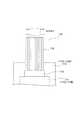
次に、図7、図8に基づいて、上記2枚のプリント基板120を備えた光トランシーバ110の概略構成を説明する。
これらの図7、図8に示すように、光トランシーバ110は、筐体111と、この筐体111の内部に間隔をおいて平行に設けられそれぞれ相手方と接続可能な電気コネクタ部112C,112Cを有する2枚のプリント基板112、すなわち、送信用プリント基板112Aと受信用プリント基板112Bとを備えている。Next, a schematic configuration of the
As shown in FIGS. 7 and 8, the
各プリント基板112A,112Bの電気コネクタ部112C,112Cと反対側の端部には、電気信号と光信号との相互変換を行う2個の光モジュール114、すなわち、送信用光モジュール114Aと受信用光モジュール114Bとが実装されている。
また、各光モジュール114A,114Bと、筐体111の前記電気コネクタ部112C,112Cと反対側の端部に装備された外部入力用の光コネクタ117とは、送信用光ファイバアレイ116Aと受信用光モジュール116Bからなる一対の光ファイバアレイ116で接続されている。そして、この光ファイバアレイ116の一端部は、光ファイバアレイ・光ファイバアレイコネクタ119に接続されている。
なお、図7は筐体111の蓋(図略)を取り外した状態を示し、また、図8に表示した上方、下方は、光トランシーバ110を通常の使用時において配置した状態での位置関係である。At the end of each printed
The
7 shows a state in which the lid (not shown) of the
この光ファイバアレイ116は図9に示すように、平面方向に1列に並んでいるのが通常である。そのため、これをねじりの方向に引き回すのは困難であり、また、破損やファイバ毎の応力不均一による特性劣化を招く蓋然性が高いため好ましくない。
したがって、光モジュール114A,114Bを傾けたり、向きを変えたりして実装することは、光コネクタ117の並びが規定されている以上難しいものとなっている。
そのため、図7、図9、図10に示すように、光コネクタ117の各ポート120の並びと平行になるように光モジュール114A,114Bを配置する必要があり、この場合、各プリント基板112A,112Bの表面に直接実装する構造をとるのが最も簡便である。As shown in FIG. 9, the
Accordingly, it is difficult to mount the
Therefore, as shown in FIGS. 7, 9, and 10, it is necessary to arrange the
一方、光送受信ポートについても、送受信併せて24ch分のポート配置として12×2の構成が上記MSAで規定されているが、図8に詳細を示すように、2個の光モジュール114、すなわち、送信用光モジュール114Aおよび受信用光モジュール114Bからの光出力ポート間(寸法D)と、上下方向に配置された2枚のプリント基板112(図8参照)の間隔とはそれぞれ大きく異なる寸法となっているため、これらの位置を調整する必要がある。 On the other hand, for the optical transmission / reception port, the 12 × 2 configuration is defined by the MSA as a port arrangement for 24 channels including transmission and reception, but as shown in detail in FIG. 8, two
しかしながら、前記特許文献1に開示された光入出力インターフェースでは、前述のように、データ転送スループット及び実装密度の向上を図れる構成となっているが、前記MSAに対応した構成については記載されていない。 However, as described above, the optical input / output interface disclosed in Patent Document 1 has a configuration capable of improving data transfer throughput and mounting density, but does not describe a configuration corresponding to the MSA. .
また、前記特許文献2に開示された光トランシーバでは、隣接チャンネル間の光学的干渉および電気的干渉を防止する構成とはなっているが、この光トランシーバでも前記MSAの特に高さに対応した構成については記載されていない。 The optical transceiver disclosed in
さらに、前記図7、図8に示す光トランシーバ110では、次のような問題がある。
すなわち、上記光トランシーバ110では、送信および受信光モジュール114A,114Bが各プリント基板112A,112B上に実装される構造となっているが、筐体111の内部の高さA、および2枚のプリント基板112A,112B間の距離Bは前記MSAにより規定されているため、各光モジュール114A,114Bの高さCによっては、プリント基板112A,112Bに直接送信光モジュール114A、受信光モジュール114Bを実装することは寸法の制約上困難である。
また、各光モジュール114A,114Bから筐体111の光コネクタ117への経路となる光ファイバアレイ116についても、最小曲率半径rの制約上、基板間距離Bに対し十分な距離Dをとらなければならなかった。その結果、光トランシーバ110を小型化するという点で問題があった。
さらに、2枚のプリント基板112A,112Bは、外部からの振動および光トランシーバ110の外部コネクタとの着脱による衝撃を直接受けるため、当該振動・衝撃による光ファイバアレイ116の破損、並びに各光モジュール114A,114Bと光ファイバアレイ116の接合部の光軸ずれを招くおそれが多い。Further, the
In other words, the
In addition, the
Further, since the two printed
本発明の目的は、上述した各課題を解決するために、それぞれ電気コネクタ部を有し平行に配置された少なくとも一対のプリント基板と、少なくとも一対の送受信用光モジュールとを、寸法が規格化された筐体内部に容易に収容でき、かつ小型化できる光トランシーバを提供することである。 In order to solve the above-described problems, the object of the present invention is to standardize the dimensions of at least a pair of printed circuit boards each having an electrical connector portion and arranged in parallel, and at least a pair of optical modules for transmission and reception. It is an object of the present invention to provide an optical transceiver that can be easily accommodated inside a housing and that can be miniaturized.
前記目的を達成するために、本発明の光トランシーバは、筐体と、この筐体の内部に相互に所定間隔をあけて平行に設けられると共に一端部にそれぞれ相手方と接続可能な電気コネクタ部を有する送信用および受信用の少なくとも一対のプリント基板と、前記筐体の内部で前記一対のプリント基板の他端部の先方で当該他端部から離れた位置にそれぞれ設けられ電気信号と光信号との相互変換を行う一対の光モジュールと、前記一対のプリント基板および前記一対の光モジュールの先方に設けられた光コネクタと、前記一対の光モジュールと前記光コネクタとを接続する少なくとも一対の光ファイバアレイと、を備えた光トランシーバであって、
前記一対の光モジュールを前記光コネクタと前記一対のプリント基板との間に配置すると共に、前記一対の光モジュールがそれぞれ表裏面に実装されるモジュール実装用基板のモジュール搭載面間の寸法を前記一対のプリント基板間の寸法よりも小さな寸法に設定したことを特徴とする。
また、本発明の他の光トランシーバは、筐体と、この筐体の内部に相互に所定間隔をあけて平行に設けられると共に一端部にそれぞれ相手方と接続可能な電気コネクタ部を有する送信用および受信用の少なくとも一対のプリント基板と、前記筐体の内部で前記一対のプリント基板の他端部の先方で当該他端部から離れた位置にそれぞれ設けられ電気信号と光信号との相互変換を行う一対の光モジュールと、前記一対のプリント基板および一対の光モジュールの先方に設けられた光コネクタと、前記一対の光モジュールと前記光コネクタとを接続する少なくとも一対の光ファイバアレイと、を備えた光トランシーバであって、
前記一対のプリント基板を、光送信用リジッド基板と光受信用リジッド基板とで構成し、
前記光送信用リジッド基板と光受信用リジッド基板との前記他端部に、当該他端部から前記光コネクタ側に延出して形成された光送信用および光受信用の一対のフレキシブル基板を設け、
これらのフレキシブル基板を、それぞれの前記光コネクタ側の一部が前記光送信用リジッド基板および光受信用リジッド基板と平行に対向配置されると共にこれらの平行な面の互いの外側面を前記一対の光モジュールが実装されるモジュール搭載面とし、
前記フレキシブル基板の前記モジュール搭載面と前記一対のプリント基板との間を曲線状に形成し、
前記モジュール搭載面間の寸法を前記一対のプリント基板間の寸法よりも小さな寸法としたことを特徴とする。
さらに、本発明の他の光トランシーバは、筐体と、この筐体の内部に相互に所定間隔をあけて平行に設けられると共に一端部にそれぞれ相手方と接続可能な電気コネクタ部を有する送信用および受信用の少なくとも一対のプリント基板と、前記筐体の内部で前記一対のプリント基板の他端部の先方で当該他端部から離れた位置にそれぞれ設けられ電気信号と光信号との相互変換を行う一対の光モジュールと、前記一対のプリント基板および一対の光モジュールの先方に設けられた光コネクタと、前記一対の光モジュールと前記光コネクタとを接続する少なくとも一対の光ファイバアレイと、を備えた光トランシーバであって、
前記一対のプリント基板を光送信用リジッド基板と光受信用リジッド基板とで構成すると共に、当該各リジッド基板の前記光コネクタ側の端部を幅方向中央部が前記電気コネクタ部側に凹んだ凹み部を有する平面形状とし、
一端部が前記光送信用リジッド基板および光受信用リジッド基板に固定されると共に、他端部が前記凹み部の奥面から前記光コネクタ側に延出しかつ前記光送信用リジッド基板および光受信用リジッド基板と平行となった光送信用および光受信用の一対のフレキシブル基板を設け、
これらのフレキシブル基板を、それぞれの前記光コネクタ側の一部が前記光送信用リジッド基板および光受信用リジッド基板と平行に対向配置されると共にこれらの平行な面の互いの外側面を前記一対の光モジュールが実装されるモジュール搭載面とし、
前記一対のフレキシブル基板の前記モジュール搭載面と前記一対のプリント基板との間を曲線状に形成し、
前記モジュール搭載面間の寸法を、前記一対のプリント基板間の寸法よりも小さな寸法としたことを特徴とする。In order to achieve the above object, an optical transceiver according to the present invention is provided with a housing and an electrical connector portion that is provided in parallel inside the housing at a predetermined interval and that can be connected to the other end at one end. a pair of printed circuit board even withoutleast for transmission and reception with the electrical signals respectively providedat a position away from the other end in the other party of the otherend of the pair of printed circuit board inside the housing and the light Apair of optical modules thatperform interconversion with signals, an optical connector provided atthe front of the pair of printed boardsand the pair of optical modules, and at least a pair of the pair of optical modules and the optical connector An optical transceiver comprising: an optical fiber array;
The pair of optical modules is disposed between the optical connector and the pair of printed boards, andthe dimension between the module mounting surfaces of the module mounting board on which thepair of optical modules aremounted on the front and back surfaces, respectively, is measured. Thedimension is set to be smaller than the dimension between the printed circuit boards.
Further, another optical transceiver of the present invention is provided for transmission and having a housing and an electrical connector portion which is provided in parallel inside the housing at a predetermined interval and can be connected to the other end at one end portion. At least a pair of printed circuit boards for reception, and an electrical signal and an optical signal, which are provided in a position away from the other end of the pair of printed circuit boards, at the tip of the other end of the pair of printed circuit boards, respectively. A pair of optical modules to be performed, an optical connector provided at the front of the pair of printed boards and the pair of optical modules, and at least a pair of optical fiber arrays connecting the pair of optical modules and the optical connector. Optical transceiver,
The pair of printed boards is composed of a rigid board for light transmission and a rigid board for light reception,
A pair of flexible substrates for optical transmission and optical reception formed by extending from the other end portion to the optical connector side is provided at the other end portion of the optical transmission rigid substrate and the optical reception rigid substrate. ,
These flexible substratesare arranged such that a part of each optical connector side isopposed to and parallel to the optical transmission rigid substrate and the optical reception rigid substrate, and the parallelouter surfaces of the parallel surfaces are the pair of the flexible substrates. With the module mounting surfaceon which the optical module is mounted ,
Forming between the module mounting surface of the flexible substrate and the pair of printed circuit boards in a curved shape,
The dimension between the module mounting surfaces is smaller than the dimension between the pair of printed circuit boards .
Furthermore, another optical transceiver of the present invention is provided for transmission and having a housing and an electrical connector portion which is provided in parallel inside the housing at a predetermined interval and can be connected to the other end at one end portion. At least a pair of printed circuit boards for reception, and an electrical signal and an optical signal, which are provided in a position away from the other end of the pair of printed circuit boards, at the tip of the other end of the pair of printed circuit boards, respectively. A pair of optical modules to be performed, an optical connector provided at the front of the pair of printed boards and the pair of optical modules, and at least a pair of optical fiber arrays connecting the pair of optical modules and the optical connector. Optical transceiver,
The pair of printed circuit boards includes a rigid board for light transmission and a rigid board for light reception, and a recess in which an end portion on the optical connector side of each rigid board is recessed in the width direction center portion on the electric connector portion side. A planar shape having a portion,
One end is fixed to the rigid substrate for optical transmission and the rigid substrate for optical reception, and the other end extends from the inner surface of the recess to the optical connector side, and therigid substrate for optical transmission and the optical reception Provide a pair of flexible substrates for light transmission and light reception parallel to the rigid substrate,
These flexible substrates are arranged such that a part of each optical connector side is opposed to and parallel to the optical transmission rigid substrate and the optical reception rigid substrate, and the parallel outer surfaces of the parallel surfaces are the pair of the flexible substrates. With the module mounting surface on which the optical module is mounted,
Forming a curvebetween the module mounting surface of the pair of flexible boardsand the pair of printed boards ;
The dimension between the module mounting surfaces is smaller than the dimension between the pair of printed boards .
本願発明の光トランシーバによれば、各光モジュールを実装した接続部材のモジュール実装面相互間の寸法が、一対のプリント基板間の寸法よりも小さな寸法となっているので、それぞれ電気コネクタ部を有し平行に配置された少なくとも一対のプリント基板と、少なくとも一対の送受信用光モジュールとを、寸法が規格化された筐体内部に容易に収容でき、かつ小型化できる。 According to the optical transceiver of the present invention, since the dimension between the module mounting surfaces of the connecting member on which each optical module is mounted is smaller than the dimension between the pair of printed boards, each has an electrical connector portion. In addition, at least a pair of printed circuit boards and at least a pair of transmission / reception optical modules arranged in parallel can be easily accommodated in a housing whose dimensions are standardized, and can be reduced in size.
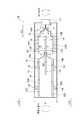
以下に、図1、図2を参照して、本発明に係る光トランシーバの第1実施形態を説明する。 A first embodiment of an optical transceiver according to the present invention will be described below with reference to FIGS.
図1、図2に示すように、本実施形態の光トランシーバ10は、例えばサーバやデータ装置間に配置して相互間での光通信を行うものである。 As shown in FIG. 1 and FIG. 2, the
この光トランシーバ10は、略直方体状の筐体11と、この筐体11の内部にそれぞれ設けられ上下方向に平行に配置された少なくとも一対のプリント基板12を構成する送信用リジッド基板12Aおよび受信用リジッド基板12Bと、一端部が上記両基板12A,12Bの上下方向略中心部に配置され他端部が両基板12A,12Bから離れる方に延出した1枚のモジュール実装用基板13と、このモジュール実装用基板13の表面に実装された少なくとも一対の光モジュール14を構成する送信用光モジュール14Aおよびモジュール実装用基板13の裏面に実装された受信用光モジュール14Bと、送信用カードエッジ基板12Aとモジュール実装用基板12Bとを接続する少なくとも一対のフレキシブル基板15を構成する送信用フレキシブル基板15Aと、受信用リジッド基板12Bとモジュール実装用基板13とを接続する受信用フレキシブル基板15Bとを備えて構成されている。
なお、モジュール実装用基板13は、リジッド基板で構成されている。The
The
ここで、送信用リジッド基板12Aおよび受信用リジッド基板12Bとモジュール実装用基板13とは、いずれもリジッド基板であるが、図1,2に示すように、一対のフレキシブル基板15を境にして、電気コネクタ部12C側と、送受信用光モジュール14A,14Bが搭載される側の2箇所にリジッド基板が存在する場合、便宜上、電気コネクタ部12C側のリジッド基板、つまり送受信用リジッド基板12A,12Bをカードエッジ基板と呼ぶことが多い。 Here, the transmitting
また、図1は筐体11の蓋(図略)を取り外した状態を示し、図2に示す上方、下方は、光トランシーバ10を通常の使用時において配置した状態での位置関係である。 FIG. 1 shows a state in which the lid (not shown) of the
筐体11の一方側の端部で高さ方向および幅方向略中央部には光コネクタ17が装備されている。
この光コネクタ17は、光通信ネットワークの信頼性、柔軟性を確保するための重要なインターフェース部品である。そして、この光コネクタ17には、一対の光ファイバアレイ16を構成すると共に送信用光モジュール14Aの光出力部に接続される送信用光ファイバアレイ16Aと、受信用光モジュール14Bの光入力部に接続される受信用光ファイバアレイ16Bとがそれぞれ連結されている。
各光ファイバアレイ16A,16Bは、互いに反対方向から曲率半径r1で折り曲げられた湾曲部を有する形状となっている。An
The
Each of the
前記各リジッド基板12A,12Bの上記光コネクタ17とは反対側の端部には電気コネクタ部12Cがそれぞれ設けられ、この電気コネクタ部12Cにより、各リジッド基板12A,12Bは相手方の装置等と挿抜自在となっている。
図2に示すように、前記送信用フレキシブル基板15Aは、送信用リジッド基板12Aの表面から前記モジュール実装用基板13の表面に向かって、つまり、下方に向かって、互いに反対方向に湾曲して設けられている。
そして、フレキシブル基板15Aの一端部が送信用リジッド基板12Aの他端部に接続されると共に、フレキシブル基板15Aの他端部がモジュール実装用基板13の一部に接続されている。As shown in FIG. 2, the transmission
One end of the
また、受信用フレキシブル基板15Bは、受信用リジッド基板12Bの表面からモジュール実装用基板13の裏面に向かって、つまり、上方に向かって、互いに反対方向に湾曲して設けられ、フレキシブル基板15Bの一端部が受信用リジッド基板12Bの他端部に接続されると共に、フレキシブル基板15Bの他端部がモジュール実装用基板13の一部に接続されている。
以上のように、送信用フレキシブル基板15Aと受信用フレキシブル基板15Bとはモジュール実装用基板13を挟んで上下方向に対称形状となって配置されている。The receiving
As described above, the transmitting
前記送信用光ファイバアレイ16Aと受信用光ファイバアレイ16Bとは、前述のように、送信用光モジュール14Aの光出力部および受信用光モジュール14Bの光入力部から前記光コネクタ17に向かって、互いに反対方向から曲率半径r1で折り曲げられて連続した形状で設けられている。 The transmission
前述のように、モジュール実装用基板13の表面には送信用光モジュール14Aが実装され、モジュール実装用基板13の裏面には受信用光モジュール14Bが実装されている。すなわち、モジュール実装用基板13の表面がモジュール搭載面13A、モジュール実装用基板13の裏面がモジュール搭載面13Bをそれぞれ構成している。
このような構成となっているので、両光モジュール14A,14Bの対向面間の距離B1がモジュール実装用基板13の厚さまで縮められている。そのため、両光モジュール14A,14Bの高さCが規定された寸法に設定されていても、筐体11を大きくすることなく、光モジュール14A,14Bを、余裕をもって収容することができる。すなわち、光モジュール14A,14Bの高さCによる制約を解消することができる。As described above, the transmission
With this configuration, the distance B1 between the opposing surfaces of the
送信用光モジュール14Aは、送信用リジッド基板12Aおよび送信用フレキシブル基板15Aを経由した電気信号を光信号に変換するものであり、その変換した光信号を、送信用光ファイバアレイ16Aおよび前記光コネクタ17を介して外部に出力するようになっている。
また、受信用光モジュール14Bは、光コネクタ17および光ファイバアレイ16Bを経由した光信号を電気信号に変換するものであり、その変換した電気信号を電気コネクタ部12Cから相手方の装置のコネクタを介して出力するようになっている。The transmission
The receiving
上述のように、送信用光モジュール14Aと受信用光モジュール14Bとがモジュール実装用基板13の表裏面に実装され、互いに上下方向に接近しているので、光モジュール14Aの出口と光モジュール14Bの入り口との距離が近くなっている。そのため、送信用光ファイバアレイ16Aと受信用光ファイバアレイ16Bの湾曲部の曲率半径r1を小さくすることができる。その結果、各光モジュール14A,14Bから光コネクタ17までの距離D1を小さくすることができるので、筐体11、ひいては光トランシーバ10をコンパクト化することができる。 As described above, the transmission
ここで、各リジッド基板12A,12Bとモジュール実装用基板13との幅寸法は略同じに形成されている。また、各フレキシブル基板15A,15Bは、モジュール実装用基板13等の幅より小さな幅寸法に形成されると共に、各リジッド基板12A,12Bおよびモジュール実装用基板13の幅方向略中央部に配置されている。
さらに、光ファイバアレイ16A,16Bの幅は、各光モジュール14A,14Bおよび光コネクタ17の幅より小さな幅寸法に形成されている。Here, the width dimensions of the
Furthermore, the widths of the
また、図2に示すように、各リジッド基板12A,12Bは、絶縁性の基板保持部材18等により筐体11に保持され、各光モジュール14A,14Bは、絶縁性の基板保持部材19等により筐体11に保持されている。 Further, as shown in FIG. 2, the
以上のような構成の第1実施形態の光トランシーバ10によれば、次のような効果が得られる。
(1)送信用および受信用リジッド基板12A,12Bと光モジュール実装用基板13とは、それぞれ送信用フレキシブル基板15Aと受信用フレキシブル基板15Bによって接続されており、光モジュール実装用基板13は、リジッド基板12A,12B間の寸法の略中間位置に配置されているので、送信用光モジュール14Aおよび受信用光モジュール14Bの実装位置の間隔をモジュール実装用基板13の厚さにまで縮めることができる。その結果、光モジュール14A,14Bを筐体11内に充分な余裕を持って収容することができて、光モジュール14A,14Bの高さCによる制約を解消することができる。そして、前記MSAの規格に適合させることができる。According to the
(1) The transmitting and receiving
(2)送信用光モジュール14Aの送信側出口と受信用光モジュール14Bの入り口とが上下方向に近づくため、送信用光ファイバアレイ16Aと受信用光ファイバアレイ16Bの湾曲部の曲率半径r1を小さくすることができる。その結果、光モジュール14A,14Bから光コネクタ17までの距離D1を小さくすることができるので、筐体11をコンパクト化することができる。(2) Since the transmission-side exit of the transmission
(3)送信用リジッド基板12Aおよび受信用リジッド基板12Bと光モジュール実装用基板13とが、それぞれ送信用フレキシブル基板15Aと受信用フレキシブル基板15Bによって接続されているので、各リジッド基板12A,12Bに外部からかかる振動・衝撃が各フレキシブル基板12A,12Bにより吸収される。その結果、筐体11にかかる振動および電気コネクタ部12Cの着脱による衝撃に対しての耐性を持たせることが可能となる。(3) Since the transmitting
(4)送受信用光モジュール14A,14Bが送受信用フレキシブル基板15A,15Bに実装され、これらのフレキシブル基板15A,15Bは送受信用リジッド基板12A,12Bの間隔の寸法内に設けられているので簡単な構成で、規格化された筐体内に容易に収容することができる。その結果、特殊な専用機構および部品を使用せずにすむので、低コスト化を図ることができる。(4) The transmission / reception
(5)各リジッド基板12A,12Bが1枚のモジュール実装用基板13に集約されるため、1系の制御系で制御することができ、また、送受信間並びに両側の電気コネクタ部12Cとの制御信号・モニタ信号の引き回しやGND(GIRL NEXT DOOR;接地)の共通化が容易となり、配線上のメリットや制御IC実装上のメリットも得られる。(5) Since each
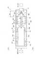
次に、図3、図4を参照して、本発明の光トランシーバの第2実施形態を説明する。
なお、本第2実施形態を示す図3、図4において、前記第1実施形態と同一部材、同一構成等と同一のものには同一符号を付し、異なる部分のみを詳細に説明する。
また、図3に示す上方、下方は、光トランシーバ20を通常の使用時において配置した状態での位置関係である。Next, a second embodiment of the optical transceiver of the present invention will be described with reference to FIGS.
In FIGS. 3 and 4 showing the second embodiment, the same members, the same configurations and the like as those in the first embodiment are denoted by the same reference numerals, and only different portions will be described in detail.
Moreover, the upper side and the lower side shown in FIG. 3 indicate the positional relationship in a state where the
本第2実施形態の光トランシーバ20は、前記第1実施形態の光トランシーバ10におけるモジュール実装用基板13を使用せず、一対のフレキシブル基板25を構成する送信用フレキシブル基板25Aと受信用フレキシブル基板25Bとに、前記送信用光モジュール14Aと受信用光モジュール14Bとをそれぞれ直接実装させたものである。 The
すなわち、本第2実施形態の光トランシーバ20では、送信用フレキシブル基板25Aと受信用フレキシブル基板25Bとの他端をそれぞれ前記光コネクタ17側に延ばし、その延ばした他端部25C,25Cに前記光モジュール14A,14Bを実装したものである。 That is, in the
各フレキシブル基板25A,25Bの他端部の先端位置は、前記モジュール実装用基板13の先端部位置と略同じ位置までの長さに形成されている。
また、他端部25C,25Cは水平面部に形成され、前記送信用リジッド基板12Aおよび受信用リジッド基板12Bと平行になっている。そして、この水平面部に形成された他端部25C,25Cが、モジュール実装面を構成している。The tip positions of the other end portions of the
The
ここで、各フレキシブル基板25A,25Bの水平面部25C,25C間の距離はB2となっている。
また、各フレキシブル基板25A,25Bの幅は、図3に示すように、送受信用リジッド基板12A,12Bの幅より小さな寸法の幅に形成されると共に、各光モジュール14A,14Bの幅よりわずかに大きな寸法の幅に形成されている。Here, the distance between the
Further, as shown in FIG. 3, the width of each
以上のような構成の第2実施形態の光トランシーバ20によれば、前記(1)〜(4)と略同様の効果を得ることができる他、次のような効果が得られる。
(6)送信用フレキシブル基板25Aと受信用フレキシブル基板25Bとの他端を前記光コネクタ17側に延ばし、その延ばした他端部に前記光モジュール14A,16が実装されているので、前記第1実施形態で使用したモジュール実装用基板13が不要となる。その結果、部品点数を少なくすることができるので、低コスト化を図ることができる。
(7)フレキシブル基板25A,25Bの幅を光モジュール14A,14Bの幅とほぼ同一にすることで,フレキシブル基板への曲げによる負荷を軽減することができる。According to the
(6) Since the other end of the transmitting
(7) By making the widths of the
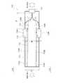
次に、図5、図6を参照して、本発明の光トランシーバの第3実施形態を説明する。
本第3実施形態を示す図5、図6において、前記各実施形態と同一部材、同一構成等と同一のものには同一符号を付し、異なる部分のみを説明する。
また、図5に示す上方、下方は、光トランシーバ30を通常の使用時において配置した状態での位置関係である。Next, a third embodiment of the optical transceiver of the present invention will be described with reference to FIGS.
In FIG. 5 and FIG. 6 showing the third embodiment, the same members, the same configurations and the like as those of the respective embodiments are denoted by the same reference numerals, and only different portions will be described.
Moreover, the upper side and the lower side shown in FIG. 5 are the positional relationships in a state where the
本第3実施形態の光トランシーバ30は、一対のフレキシブル基板35を構成する送信用フレキシブル基板35Aおよび受信用フレキシブル基板35Bの幅を、前記送信用光モジュール14Aおよび受信用光モジュール14Bの幅とほぼ同一にすると共に、送信用フレキシブル基板35Aおよび受信用フレキシブル基板35Bの他端部を前記光コネクタ17側に延出したものである。 In the
すなわち、送信用フレキシブル基板35Aおよび受信用フレキシブル基板35Bが、前記本第2実施形態のフレキシブル基板25A,25Bと同様の形状に形成されており、これに対して、一対のリジッド基板32を構成する送信用リジッド基板32Aと受信用リジッド基板32Bとの延出他端部32Dが、各フレキシブル基板35A,35Bを挟むように配置されている。つまり、各リジッド基板32A,32Bの他端部の平面形状が筐体11の一端側に凹んだ凹部32Eとなっており、この凹部32E内に各フレキシブル基板35A,35Bが配置されていることになる。
そして、これらのフレキシブル基板35A,35Bの互いに反対方向の表面が各光モジュール14A,14Bが実装されるモジュール実装面35Cとなっている。
また、各リジッド基板32A,32Bの一端部には電気コネクタ部32Cが設けられている。
ここで、各フレキシブル基板35A,35Bの幅は、各光モジュール14A,14Bの幅よりわずかに大きな寸法の幅に形成されている。That is, the transmission
The surfaces of these
In addition, an
Here, the width of each
以上のような構成の第3実施形態の光トランシーバ30によれば、前記(1)〜(4)、(6)、(7)と略同様の効果を得ることができる他、次のような効果が得られる。
(7)送信用リジッド基板12Aと受信用リジッド基板12Bとに、光コネクタ17側に延出した延出他端部32Dが形成されているので、その延出他端部32DをIC実装領域および配線可能領域とすることができ、その結果、より自由度の高い設計ができる。According to the
(7) Since the transmitting
以上、上記各実施形態を参照して本発明を説明したが、本発明は上記各実施形態に限定されるものではない。本発明の構成や詳細については、当業者が理解し得るさまざまな変更を加えることができる。また、本発明には、上記各実施形態の構成の一部又は全部を相互に適宜組み合わせたものも含まれる。 Although the present invention has been described with reference to the above embodiments, the present invention is not limited to the above embodiments. Various changes that can be understood by those skilled in the art can be made to the configuration and details of the present invention. Further, the present invention includes a combination of some or all of the configurations of the above-described embodiments as appropriate.
例えば、前記各実施形態では、プリント基板として、送信用リジッド基板12Aと受信用リジッド基板12Bとの2枚で構成したが、より多くの複数の基板等についても適用することができる。
すなわち、電気コネクタ12C側の送受信用リジッド基板12A,12Bを3枚以上で構成した場合、光入出力が3列以上、あるいは光モジュールが3つ以上となった場合等にも適用することができる。For example, in each of the above-described embodiments, the printed circuit board is composed of the transmission
In other words, when the transmission / reception
また、前記各実施形態では、プリント基板として送信用リジッド基板12Aと受信用リジッド基板12Bとの2枚で構成し、さらに各リジッド基板12A,12Bとモジュール実装用基板13とを各フレキシブル基板15A,15B等とでそれぞれ接続したが、これに限らない。各リジッド基板12A,12Bと各フレキシブル基板15A,15B等とに変えてリジッドフレキシブル基板を使用してもよい。
この場合、リジッド部とフレキシブル部が一体化されるため、リジッド基板とフレキシブル基板の接合部による信号劣化等を防ぐことができ、優れた特性面を得ることができる。
そのうえ、リジッド部とフレキシブル部が一体化されたリジッドフレキシブル基板を使用した場合、フレキシブル基板15A,15B等が不要となり、これにより省部材化を図ることができる。Further, in each of the above-described embodiments, the printed board is composed of two boards, that is, a transmission
In this case, since the rigid portion and the flexible portion are integrated, it is possible to prevent signal deterioration due to the joint portion between the rigid substrate and the flexible substrate, and to obtain an excellent characteristic surface.
In addition, when a rigid flexible substrate in which the rigid portion and the flexible portion are integrated is used, the
さらに、前記各実施形態では、送信用各部材、つまり送信用リジッド基板12A、送信用フレキシブル基板15A,25A,35A、送信用フレキシブル基板15A、送信用光モジュール14A、送信用光ファイバアレイ16Aを、光トランシーバ10の通常使用状態で上方側に配置し、受送信用各部材、つまり受信用リジッド基板12B等を光トランシーバ10の通常使用状態で下方側に配置してあるが、これに限らない。両者を逆に配置、つまり、送信用各部材を光トランシーバ10の下方側に配置すると共に受送信用各部材を上方側に配置してもよい。 Further, in each of the above embodiments, each member for transmission, that is, the rigid substrate for
(付記1)
筐体と、この筐体の内部に相互に所定間隔をあけて平行に設けられると共に一端部にそれぞれ相手方と接続可能な電気コネクタ部を有する送信用および受信用の少なくとも一対のプリント基板と、前記筐体の内部で前記一対のプリント基板の他端部の先方で当該他端部から離れた位置にそれぞれ設けられ電気信号と光信号との相互変換を行う一対の光モジュールと、前記一対のプリント基板および前記一対の光モジュールの先方に設けられた光コネクタと、前記一対の光モジュールと前記光コネクタとを接続する少なくとも一対の光ファイバアレイと、を備えた光トランシーバであって、
前記一対の光モジュールを前記光コネクタと前記一対のプリント基板との間に配置すると共に、前記一対の光モジュールがそれぞれ表裏面に実装されるモジュール実装用基板のモジュール搭載面間の寸法を前記一対のプリント基板間の寸法よりも小さな寸法に設定したことを特徴とする光トランシーバ。(Appendix 1)
A housing, a pair of printed circuit board even withoutleast for transmission and reception of the respectively mutually inside the housing at one end with provided in parallel at predetermined intervals having an electrical connector portion connectable to a counterpart Apair of optical modulesthat are provided atpositions away from the other endof the pair of printed circuit boards inside the casing and thatperform mutual conversion between an electrical signal and an optical signal, and the pair An optical transceiver comprising: an optical connector provided atthe front of the printed circuit boardand the pair of optical modules; and at least a pair of optical fiber arrays connecting the pair of optical modules and the optical connector,
The pair of optical modules is disposed between the optical connector and the pair of printed boards, andthe dimension between the module mounting surfaces of the module mounting board on which thepair of optical modules aremounted on the front and back surfaces, respectively, is measured. An optical transceiver characterizedin that it isset to a size smaller than the size between printed circuit boards.
(付記2)
付記1に記載した光トランシーバにおいて、
前記モジュール搭載面を前記一対のプリント基板と平行に形成したことを特徴とする光トランシーバ。(Appendix 2)
In the optical transceiver described in Appendix 1,
An optical transceiver characterized in that themodule mounting surface is formed in parallel with the pair of printed circuit boards.
(付記3)
付記1または付記2に記載した光トランシーバにおいて、
前記一対のプリント基板を、光送信用リジッド基板と光受信用リジッド基板とで構成し、
前記モジュール実装用基板と、前記光送信用リジッド基板および光受信用リジッド基板とを、光送信用および光受信用の一対のフレキシブル基板で接続したことを特徴とする光トランシーバ。(Appendix 3)
In the optical transceiver described in appendix 1 or
The pair of printed boards is composed of a rigid board for light transmission and a rigid board for light reception,
An optical transceiver, wherein themodule mounting substrate, the optical transmission rigid substrate and the optical reception rigid substrateareconnected by a pair of flexible substrates for optical transmission and optical reception.
(付記4)
付記3に記載した光トランシーバにおいて、
前記光送信用フレキシブル基板と光受信用フレキシブル基板との幅をそれぞれ前記光送信用リジッド基板および光受信用リジッド基板の幅より小さな幅としたことを特徴とする光トランシーバ。(Appendix 4)
In the optical transceiver described in Appendix 3,
An optical transceiver characterized in that a width of the flexible substrate for optical transmission and a flexible substrate for optical reception are made smaller than the width of the rigid substrate for optical transmission and the rigid substrate for optical reception, respectively.
(付記5)
筐体と、この筐体の内部に相互に所定間隔をあけて平行に設けられると共に一端部にそれぞれ相手方と接続可能な電気コネクタ部を有する送信用および受信用の少なくとも一対のプリント基板と、前記筐体の内部で前記一対のプリント基板の他端部の先方で当該他端部から離れた位置にそれぞれ設けられ電気信号と光信号との相互変換を行う一対の光モジュールと、前記一対のプリント基板および一対の光モジュールの先方に設けられた光コネクタと、前記一対の光モジュールと前記光コネクタとを接続する少なくとも一対の光ファイバアレイと、を備えた光トランシーバであって、
前記一対のプリント基板を、光送信用リジッド基板と光受信用リジッド基板とで構成し、
前記光送信用リジッド基板と光受信用リジッド基板との前記他端部に、当該他端部から前記光コネクタ側に延出して形成された光送信用および光受信用の一対のフレキシブル基板を設け、
これらのフレキシブル基板を、それぞれの前記光コネクタ側の一部が前記光送信用リジッド基板および光受信用リジッド基板と平行に対向配置されると共にこれらの平行な面の互いの外側面を前記一対の光モジュールが実装されるモジュール搭載面とし、
前記フレキシブル基板の前記モジュール搭載面と前記一対のプリント基板との間を曲線状に形成し、
前記モジュール搭載面間の寸法を前記一対のプリント基板間の寸法よりも小さな寸法としたことを特徴とする光トランシーバ。(Appendix 5)
A housing, and at least a pair of printed circuit boards for transmission and reception each having an electrical connector portion which is provided in parallel inside the housing at a predetermined interval and can be connected to the other end at the one end, and A pair of optical modules that are provided at positions away from the other end portion of the pair of printed circuit boards inside the housing and that perform mutual conversion between electrical signals and optical signals, and the pair of prints An optical transceiver comprising: an optical connector provided on a front side of a substrate and a pair of optical modules; and at least a pair of optical fiber arrays connecting the pair of optical modules and the optical connector;
The pair of printed boards is composed of a rigid board for light transmission and a rigid board for light reception,
A pair of flexible substrates for optical transmission and optical reception formed by extending from the other end portion to the optical connector side is provided at the other end portion of the optical transmission rigid substrate and the optical reception rigid substrate. ,
These flexible substratesare arranged such that a part of each optical connector side isopposed to and parallel to the optical transmission rigid substrate and the optical reception rigid substrate, and the parallelouter surfaces of the parallel surfaces are the pair of the flexible substrates. With the module mounting surfaceon which the optical module is mounted ,
Forming between the module mounting surface of the flexible substrate and the pair of printed circuit boards in a curved shape,
An optical transceiver characterized in that adimension between the module mounting surfaces is smaller than a dimension between the pair of printed circuit boards .
(付記6)
付記5に記載した光トランシーバにおいて、
前記一対のフレキシブル基板の幅をそれぞれ前記光送信用リジッド基板と光受信用リジッド基板の幅より小さな幅とすると共に前記各光モジュールの幅より大きな幅寸法に形成したことを特徴とする光トランシーバ。(Appendix 6)
In the optical transceiver described in Appendix 5,
An optical transceiver characterized in that a width of each of the pair of flexible substrates is smaller than a width of each of the rigid substrate for optical transmission and a rigid substrate for optical reception andlarger than thewidth of each of the optical modules.
(付記7)
筐体と、この筐体の内部に相互に所定間隔をあけて平行に設けられると共に一端部にそれぞれ相手方と接続可能な電気コネクタ部を有する送信用および受信用の少なくとも一対のプリント基板と、前記筐体の内部で前記一対のプリント基板の他端部の先方で当該他端部から離れた位置にそれぞれ設けられ電気信号と光信号との相互変換を行う一対の光モジュールと、前記一対のプリント基板および一対の光モジュールの先方に設けられた光コネクタと、前記一対の光モジュールと前記光コネクタとを接続する少なくとも一対の光ファイバアレイと、を備えた光トランシーバであって、
前記一対のプリント基板を光送信用リジッド基板と光受信用リジッド基板とで構成すると共に、当該各リジッド基板の前記光コネクタ側の端部を幅方向中央部が前記電気コネクタ部側に凹んだ凹み部を有する平面形状とし、
一端部が前記光送信用リジッド基板および光受信用リジッド基板に固定されると共に、他端部が前記凹み部の奥面から前記光コネクタ側に延出しかつ前記光送信用リジッド基板および光受信用リジッド基板と平行となった光送信用および光受信用の一対のフレキシブル基板を設け、
これらのフレキシブル基板を、それぞれの前記光コネクタ側の一部が前記光送信用リジッド基板および光受信用リジッド基板と平行に対向配置されると共にこれらの平行な面の互いの外側面を前記一対の光モジュールが実装されるモジュール搭載面とし、
前記一対のフレキシブル基板の前記モジュール搭載面と前記一対のプリント基板との間を曲線状に形成し、
前記モジュール搭載面間の寸法を、前記一対のプリント基板間の寸法よりも小さな寸法としたことを特徴とする光トランシーバ。(Appendix 7)
A housing, and at least a pair of printed circuit boards for transmission and reception each having an electrical connector portion which is provided in parallel inside the housing at a predetermined interval and can be connected to the other end at the one end, and A pair of optical modules that are provided at positions away from the other end portion of the pair of printed circuit boards inside the housing and that perform mutual conversion between electrical signals and optical signals, and the pair of prints An optical transceiver comprising: an optical connector provided on a front side of a substrate and a pair of optical modules; and at least a pair of optical fiber arrays connecting the pair of optical modules and the optical connector;
The pair of printed circuit boards includes a rigid board for light transmission and a rigid board for light reception, and a recess in which an end portion on the optical connector side of each rigid board is recessed in the width direction center portion on the electric connector portion side. A planar shape having a portion,
One end is fixed to the rigid substrate for optical transmission and the rigid substrate for optical reception, and the other end extends from the inner surface of the recess to the optical connector side, and therigid substrate for optical transmission and the optical reception Provide a pair of flexible substrates for light transmission and light reception parallel to the rigid substrate,
These flexible substrates are arranged such that a part of each optical connector side is opposed to and parallel to the optical transmission rigid substrate and the optical reception rigid substrate, and the parallel outer surfaces of the parallel surfaces are the pair of the flexible substrates. With the module mounting surface on which the optical module is mounted,
Forming a curvebetween the module mounting surface of the pair of flexible boardsand the pair of printed boards ;
An optical transceiver characterized in that adimension between the module mounting surfaces is smaller than a dimension between the pair of printed circuit boards .
(付記8)
付記7に記載した光トランシーバにおいて、
前記光送信用フレキシブル基板および光受信用フレキシブル基板の幅を前記一対の光モジュールの幅より大きな幅寸法に形成したことを特徴とする光トランシーバ。(Appendix 8)
In the optical transceiver described in
An optical transceiver, wherein a width of the flexible substrate for optical transmission and a flexible substrate for optical reception are formed to belarger than thewidth of the pair of optical modules.
本願発明は、複数の送受信用プリント基板および送受信用光モジュールを、寸法が規格化された筐体内部に収容する際に利用できる。 The present invention can be used when a plurality of transmission / reception printed circuit boards and transmission / reception optical modules are accommodated in a housing whose dimensions are standardized.
10 光トランシーバ(第1実施形態)
11 筐体
12 一対のプリント基板を構成するリジッド基板
12A 送信用リジッド基板
12B 受信用リジッド基板
12C 電気コネクタ部(カードエッジ部)
13 光モジュール実装用基板
13A 光モジュール実装面(送信用)
13B 光モジュール実装面(受信用)
14 一対の光モジュール
14A 送信用光モジュール
14B 受信用光モジュール
15 一対のフレキシブル基板
15A 送信用フレキシブル基板
15B 受信用フレキシブル基板
16 一対の光ファイバアレイ
16A 送信用光ファイバアレイ
16B 受信用光ファイバアレイ
17 光コネクタ
20 光トランシーバ(第2実施形態)
25 一対のフレキシブル基板
25A 送信用フレキシブル基板
25B 受信用フレキシブル基板
25C 光モジュール実装面
38 受信用フレキシブル基板
30 光トランシーバ(第3実施形態)
32 一対のリジッド基板
32A 送信用リジッド基板
32B 受信用リジッド基板
32D 延出他端部
32E 凹部
35 一対のフレキシブル基板
35A 送信用フレキシブル基板
35B 受信用フレキシブル基板
35C 光モジュール実装面10 Optical transceiver (first embodiment)
DESCRIPTION OF
13 Optical
13B Optical module mounting surface (for reception)
14 A pair of
25 A pair of
32 A pair of
Claims (8)
Translated fromJapanese前記一対の光モジュールを前記光コネクタと前記一対のプリント基板との間に配置すると共に、前記一対の光モジュールがそれぞれ表裏面に実装されるモジュール実装用基板のモジュール搭載面間の寸法を前記一対のプリント基板間の寸法よりも小さな寸法としたことを特徴とする光トランシーバ。A housing, and at least a pair of printed circuit boards for transmission and reception each having an electrical connector portion which is provided in parallel inside the housing at a predetermined interval and can be connected to the other end at the one end, and A pair of optical modules that are provided at positions away from the other end portion of the pair of printed circuit boards inside the housing and that perform mutual conversion between electrical signals and optical signals, and the pair of prints An optical transceiver comprising: an optical connector provided on a front side of a substrate and a pair of optical modules; and at least a pair of optical fiber arrays connecting the pair of optical modules and the optical connector;
The pair of optical modules is disposed between the optical connector and the pair of printed boards, and the dimension between the module mounting surfaces of the module mounting board on which the pair of optical modules are mounted on the front and back surfaces, respectively, is measured. An optical transceiver characterized in that the size is smaller than the size between printed circuit boards.
前記モジュール搭載面を前記一対のプリント基板と平行に形成したことを特徴とする光トランシーバ。The optical transceiver according to claim 1,
An optical transceiver characterized in that the module mounting surface is formed in parallel with the pair of printed circuit boards.
前記一対のプリント基板を、光送信用リジッド基板と光受信用リジッド基板とで構成し、
前記モジュール実装用基板と、前記光送信用リジッド基板および光受信用リジッド基板とを、光送信用および光受信用の一対のフレキシブル基板で接続したことを特徴とする光トランシーバ。The optical transceiver according to claim 1 or claim 2,
The pair of printed boards is composed of a rigid board for light transmission and a rigid board for light reception,
An optical transceiver, wherein the module mounting substrate, the optical transmission rigid substrate and the optical reception rigid substrate are connected by a pair of flexible substrates for optical transmission and optical reception.
前記光送信用フレキシブル基板と光受信用フレキシブル基板との幅をそれぞれ前記光送信用リジッド基板および光受信用リジッド基板の幅より小さな幅としたことを特徴とする光トランシーバ。The optical transceiver according to claim 3,
An optical transceiver characterized in that a width of the flexible substrate for optical transmission and a flexible substrate for optical reception are made smaller than the width of the rigid substrate for optical transmission and the rigid substrate for optical reception, respectively.
前記一対のプリント基板を、光送信用リジッド基板と光受信用リジッド基板とで構成し、
前記光送信用リジッド基板と光受信用リジッド基板との前記他端部に、当該他端部から前記光コネクタ側に延出して形成された光送信用および光受信用の一対のフレキシブル基板を設け、
これらのフレキシブル基板を、それぞれの前記光コネクタ側の一部が前記光送信用リジッド基板および光受信用リジッド基板と平行に対向配置されると共にこれらの平行な面の互いの外側面を前記一対の光モジュールが実装されるモジュール搭載面とし、
前記フレキシブル基板の前記モジュール搭載面と前記一対のプリント基板との間を曲線状に形成し、
前記モジュール搭載面間の寸法を前記一対のプリント基板間の寸法よりも小さな寸法としたことを特徴とする光トランシーバ。A housing, and at least a pair of printed circuit boards for transmission and reception each having an electrical connector portion which is provided in parallel inside the housing at a predetermined interval and can be connected to the other end at the one end, and A pair of optical modules that are provided at positions away from the other end portion of the pair of printed circuit boards inside the housing and that perform mutual conversion between electrical signals and optical signals, and the pair of prints An optical transceiver comprising: an optical connector provided on a front side of a substrate and a pair of optical modules; and at least a pair of optical fiber arrays connecting the pair of optical modules and the optical connector;
The pair of printed boards is composed of a rigid board for light transmission and a rigid board for light reception,
A pair of flexible substrates for optical transmission and optical reception formed by extending from the other end portion to the optical connector side is provided at the other end portion of the optical transmission rigid substrate and the optical reception rigid substrate. ,
These flexible substratesare arranged such that a part of each optical connector side isopposed to and parallel to the optical transmission rigid substrate and the optical reception rigid substrate, and the parallelouter surfaces of the parallel surfaces are the pair of the flexible substrates. With the module mounting surfaceon which the optical module is mounted ,
Forming between the module mounting surface of the flexible substrate and the pair of printed circuit boards in a curved shape,
An optical transceiver characterized in that adimension between the module mounting surfaces is smaller than a dimension between the pair of printed circuit boards .
前記一対のフレキシブル基板の幅をそれぞれ前記光送信用リジッド基板と光受信用リジッド基板の幅より小さな幅とすると共に前記各光モジュールの幅より大きな幅寸法に形成したことを特徴とする光トランシーバ。The optical transceiver according to claim 5,
An optical transceiver characterized in that a width of each of the pair of flexible substrates is smaller than a width of each of the rigid substrate for optical transmission and a rigid substrate for optical reception and larger than the width of each of the optical modules.
前記一対のプリント基板を光送信用リジッド基板と光受信用リジッド基板とで構成すると共に、当該各リジッド基板の前記光コネクタ側の端部を幅方向中央部が前記電気コネクタ部側に凹んだ凹み部を有する平面形状とし、
一端部が前記光送信用リジッド基板および光受信用リジッド基板に固定されると共に、他端部が前記凹み部の奥面から前記光コネクタ側に延出しかつ前記光送信用リジッド基板および光受信用リジッド基板と平行となった光送信用および光受信用の一対のフレキシブル基板を設け、
これらのフレキシブル基板を、それぞれの前記光コネクタ側の一部が前記光送信用リジッド基板および光受信用リジッド基板と平行に対向配置されると共にこれらの平行な面の互いの外側面を前記一対の光モジュールが実装されるモジュール搭載面とし、
前記一対のフレキシブル基板の前記モジュール搭載面と前記一対のプリント基板との間を曲線状に形成し、
前記モジュール搭載面間の寸法を、前記一対のプリント基板間の寸法よりも小さな寸法としたことを特徴とする光トランシーバ。A housing, and at least a pair of printed circuit boards for transmission and reception each having an electrical connector portion which is provided in parallel inside the housing at a predetermined interval and can be connected to the other end at the one end, and A pair of optical modules that are provided at positions away from the other end portion of the pair of printed circuit boards inside the housing and that perform mutual conversion between electrical signals and optical signals, and the pair of prints An optical transceiver comprising: an optical connector provided on a front side of a substrate and a pair of optical modules; and at least a pair of optical fiber arrays connecting the pair of optical modules and the optical connector;
The pair of printed circuit boards includes a rigid board for light transmission and a rigid board for light reception, and a recess in which an end portion on the optical connector side of each rigid board is recessed in the width direction center portion on the electric connector portion side. A planar shape having a portion,
One end is fixed to the rigid substrate for optical transmission and the rigid substrate for optical reception, and the other end extends from the inner surface of the recess to the optical connector side, and therigid substrate for optical transmission and the optical reception Provide a pair of flexible substrates for light transmission and light reception parallel to the rigid substrate,
These flexible substrates are arranged such that a part of each optical connector side is opposed to and parallel to the optical transmission rigid substrate and the optical reception rigid substrate, and the parallel outer surfaces of the parallel surfaces are the pair of the flexible substrates. With the module mounting surface on which the optical module is mounted,
Forming a curvebetween the module mounting surface of the pair of flexible boardsand the pair of printed boards ;
An optical transceiver characterized in that adimension between the module mounting surfaces is smaller than a dimension between the pair of printed circuit boards .
前記光送信用フレキシブル基板および光受信用フレキシブル基板の幅を前記一対の光モジュールの幅より大きな幅寸法に形成したことを特徴とする光トランシーバ。The optical transceiver according to claim 7,
An optical transceiver, wherein a width of the flexible substrate for optical transmission and a flexible substrate for optical reception are formed to be larger than the width of the pair of optical modules.
Priority Applications (2)
| Application Number | Priority Date | Filing Date | Title |
|---|---|---|---|
| JP2011017229AJP5655594B2 (en) | 2011-01-28 | 2011-01-28 | Optical transceiver |
| US13/356,105US8511913B2 (en) | 2011-01-28 | 2012-01-23 | Optical transceiver |
Applications Claiming Priority (1)
| Application Number | Priority Date | Filing Date | Title |
|---|---|---|---|
| JP2011017229AJP5655594B2 (en) | 2011-01-28 | 2011-01-28 | Optical transceiver |
Publications (2)
| Publication Number | Publication Date |
|---|---|
| JP2012159539A JP2012159539A (en) | 2012-08-23 |
| JP5655594B2true JP5655594B2 (en) | 2015-01-21 |
Family
ID=46577428
Family Applications (1)
| Application Number | Title | Priority Date | Filing Date |
|---|---|---|---|
| JP2011017229AExpired - Fee RelatedJP5655594B2 (en) | 2011-01-28 | 2011-01-28 | Optical transceiver |
Country Status (2)
| Country | Link |
|---|---|
| US (1) | US8511913B2 (en) |
| JP (1) | JP5655594B2 (en) |
Families Citing this family (6)
| Publication number | Priority date | Publication date | Assignee | Title |
|---|---|---|---|---|
| US20150003839A1 (en)* | 2012-01-13 | 2015-01-01 | Yuuji Minota | Optical transceiver |
| US9753881B2 (en)* | 2013-03-14 | 2017-09-05 | National Instruments Corporation | FPGA based ATCA (Advanced Telecommunications Computing Architecture) platform |
| US20160226591A1 (en) | 2015-02-04 | 2016-08-04 | International Business Machines Corporation | Integrated parallel optical transceiver |
| EP3121630B1 (en)* | 2015-07-21 | 2023-04-05 | Tyco Electronics Svenska Holdings AB | Optoelectronic module with improved heat management |
| JP2017090657A (en)* | 2015-11-10 | 2017-05-25 | ヒロセ電機株式会社 | Connector with optical fiber cable |
| JP2021067851A (en)* | 2019-10-24 | 2021-04-30 | 日東電工株式会社 | Optical transceiver |
Family Cites Families (12)
| Publication number | Priority date | Publication date | Assignee | Title |
|---|---|---|---|---|
| US10008A (en)* | 1853-09-13 | India-rtjbbee | ||
| JPH0843691A (en) | 1994-07-27 | 1996-02-16 | Hitachi Ltd | Optical I / O interface |
| US6901221B1 (en)* | 1999-05-27 | 2005-05-31 | Jds Uniphase Corporation | Method and apparatus for improved optical elements for vertical PCB fiber optic modules |
| US6213651B1 (en)* | 1999-05-26 | 2001-04-10 | E20 Communications, Inc. | Method and apparatus for vertical board construction of fiber optic transmitters, receivers and transceivers |
| US6952532B2 (en)* | 1999-05-27 | 2005-10-04 | Jds Uniphase Corporation | Method and apparatus for multiboard fiber optic modules and fiber optic module arrays |
| US7116912B2 (en)* | 1999-05-27 | 2006-10-03 | Jds Uniphase Corporation | Method and apparatus for pluggable fiber optic modules |
| US7594766B1 (en)* | 2002-11-15 | 2009-09-29 | Finisar Corporation | Integrated optical transceiver array |
| US7435105B2 (en)* | 2004-03-29 | 2008-10-14 | Finisar Corporation | Electrical connector for use in an optical transceiver module |
| US20050265650A1 (en)* | 2004-05-27 | 2005-12-01 | Sunil Priyadarshi | Small profile, pluggable optical transceiver subassembly |
| US7347634B2 (en)* | 2004-08-06 | 2008-03-25 | Finisar Corporation | Opto-electrical module for optical signals from at least two optical data channels for arranging on a main circuit board of a component assembly and opto-electrical component assembly |
| JP4687621B2 (en)* | 2006-09-08 | 2011-05-25 | 日立電線株式会社 | Communication module with switch function and communication device |
| KR100869701B1 (en) | 2006-12-06 | 2008-11-21 | 옵티시스 주식회사 | Optical transceiver |
- 2011
- 2011-01-28JPJP2011017229Apatent/JP5655594B2/ennot_activeExpired - Fee Related
- 2012
- 2012-01-23USUS13/356,105patent/US8511913B2/ennot_activeExpired - Fee Related
Also Published As
| Publication number | Publication date |
|---|---|
| US20120195558A1 (en) | 2012-08-02 |
| JP2012159539A (en) | 2012-08-23 |
| US8511913B2 (en) | 2013-08-20 |
Similar Documents
| Publication | Publication Date | Title |
|---|---|---|
| JP5655594B2 (en) | Optical transceiver | |
| US7645075B2 (en) | Optical connection structure of optical backplane to circuit substrate | |
| JP5770373B2 (en) | Multi-channel RF feedthrough | |
| JP4706611B2 (en) | Optical transceiver | |
| JP4964127B2 (en) | Modular optical device package | |
| CN101379662B (en) | Connection structure of photoelectric flexible wiring board, connector and photoelectric flexible wiring board | |
| US20070092185A1 (en) | Optical connection structure between optical backplane and circuit substrate | |
| US11105990B2 (en) | Optical transceiver module and optical cable module | |
| US11409062B2 (en) | Optical transceiver module and optical cable module | |
| JP2015055834A (en) | Optical transceiver | |
| JP2006030868A (en) | Photoelectric composite connector and board using the same | |
| JP2009141166A (en) | Optical transceiver and host substrate to which optical transceiver is connected | |
| US9011024B2 (en) | Optical communication module and assembling method thereof | |
| JP6988322B2 (en) | Package for optical receiver module | |
| US20110294308A1 (en) | Substrate and ic socket | |
| JPWO2013105663A1 (en) | Optical transceiver | |
| CN110719687A (en) | Apparatus and method for improved network connectivity | |
| JP6223671B2 (en) | Optical module | |
| EP3106905A1 (en) | Mid board optical module (mbom) primary heat sink | |
| TWI381661B (en) | Small form-factor pluggable transceiver module | |
| US11817905B2 (en) | Optical transceiver | |
| JP6375155B2 (en) | Optical module | |
| US9405082B2 (en) | OSA cage with reinforced connection to PCB | |
| KR101419503B1 (en) | optical and electric connector unit of electronic device having unified optical and electric transceiver for interfacing to external device | |
| JP2012063460A (en) | Optical transmission and reception module |
Legal Events
| Date | Code | Title | Description |
|---|---|---|---|
| A621 | Written request for application examination | Free format text:JAPANESE INTERMEDIATE CODE: A621 Effective date:20131204 | |
| A131 | Notification of reasons for refusal | Free format text:JAPANESE INTERMEDIATE CODE: A131 Effective date:20140527 | |
| A977 | Report on retrieval | Free format text:JAPANESE INTERMEDIATE CODE: A971007 Effective date:20140528 | |
| A521 | Request for written amendment filed | Free format text:JAPANESE INTERMEDIATE CODE: A523 Effective date:20140728 | |
| A131 | Notification of reasons for refusal | Free format text:JAPANESE INTERMEDIATE CODE: A131 Effective date:20140812 | |
| A521 | Request for written amendment filed | Free format text:JAPANESE INTERMEDIATE CODE: A523 Effective date:20141010 | |
| TRDD | Decision of grant or rejection written | ||
| A01 | Written decision to grant a patent or to grant a registration (utility model) | Free format text:JAPANESE INTERMEDIATE CODE: A01 Effective date:20141028 | |
| A61 | First payment of annual fees (during grant procedure) | Free format text:JAPANESE INTERMEDIATE CODE: A61 Effective date:20141110 | |
| R150 | Certificate of patent or registration of utility model | Ref document number:5655594 Country of ref document:JP Free format text:JAPANESE INTERMEDIATE CODE: R150 | |
| LAPS | Cancellation because of no payment of annual fees |