JP5654316B2 - Optical module - Google Patents
Optical moduleDownload PDFInfo
- Publication number
- JP5654316B2 JP5654316B2JP2010243924AJP2010243924AJP5654316B2JP 5654316 B2JP5654316 B2JP 5654316B2JP 2010243924 AJP2010243924 AJP 2010243924AJP 2010243924 AJP2010243924 AJP 2010243924AJP 5654316 B2JP5654316 B2JP 5654316B2
- Authority
- JP
- Japan
- Prior art keywords
- substrate
- groove
- optical
- mirror
- core
- Prior art date
- Legal status (The legal status is an assumption and is not a legal conclusion. Google has not performed a legal analysis and makes no representation as to the accuracy of the status listed.)
- Active
Links
Images


Landscapes
- Optical Couplings Of Light Guides (AREA)
- Semiconductor Lasers (AREA)
Description
Translated fromJapanese本発明は、光信号を送信あるいは受信する光モジュールに関する。 The present invention relates to an optical module that transmits or receives an optical signal.
データ通信の高速大容量化に伴い、従来のメタルケーブルを用いた電気信号通信に代わって、光ファイバー(光導波路を含む。)用いた光信号化が普及している。 With the increase in data communication speed and capacity, optical signal conversion using optical fibers (including optical waveguides) has become widespread in place of conventional electrical signal communication using metal cables.
光信号化は、電磁ノイズレス、高速、広帯域での絶縁信号伝送、省配線等のメリットもあり、近年では機器内通信への展開がめざましい。 Optical signalization has advantages such as electromagnetic noise-less, high-speed, wideband isolated signal transmission, reduced wiring, etc., and in recent years, it has been dramatically expanded to in-device communication.
機器内への組み込みには、光モジュールの小型、低背化は必須であり、これを実現する手段として、光素子(発光素子若しくは受光素子)を基板に実装し、その真下に光路変換するためのミラー部と、光信号伝送用の光ファイバー若しくは光導波路とを集積するモジュール形態がある。 In order to incorporate it into equipment, it is essential to reduce the size and height of the optical module. As a means to achieve this, an optical element (light-emitting element or light-receiving element) is mounted on a substrate and the optical path is converted directly below it. There is a module form in which the mirror part and an optical signal transmission optical fiber or an optical waveguide are integrated.
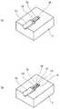
例えば、図12に示す光モジュールでは、基板51の上に、受光素子52を支持した受光素子基板53を取付け、多チャンネル化のために、複数本の光ファイバー54を受光素子基板53の各V溝55でそれぞれ位置決めして、光ファイバー保持基板56で各光ファイバー54を保持する。また、光ファイバー保持基板56の凹溝56aに反射壁面(ミラー部)56bを形成する。そして、各光ファイバー54からの出射光を反射壁面56bで反射して受光素子52に投射するようになっている(特許文献1参照)。 For example, in the optical module shown in FIG. 12, a light
ここで、各光ファイバー54の中を伝搬する光信号は、外部に漏れ出すことはほとんどない。 Here, the optical signal propagating through each
しかしながら、凹溝56aによって、各光ファイバー(チャンネル)54が光学的に繋がっているため、反射壁面(ミラー部)56bの反射光の散乱成分が、隣接する光ファイバー54に漏洩(クロストーク)しやすくなる。したがって、データ通信の高速大容量化や双方向通信に対応するための多チャンネル化に対応できないという問題があった。 However, since each optical fiber (channel) 54 is optically connected by the
本発明は、前記問題を解消するためになされたもので、ミラー部の反射光の散乱成分が隣接するチャンネルに漏洩(クロストーク)し難くできる光モジュールを提供することを目的とするものである。 The present invention has been made to solve the above problem, and an object of the present invention is to provide an optical module in which the scattering component of the reflected light of the mirror part can hardly leak (crosstalk) to an adjacent channel. .
前記課題を解決するために、本発明は、基板の表面に形成された溝内に設けられた内部導波路と、この溝の先端部に形成された光路変換用のミラー部と、このミラー部と対向するように基板の表面に実装され、ミラー部を介して内部導波路のコア部に光信号を発光し、若しくはミラー部を介して内部導波路のコア部からの光信号を受光する光素子と、内部導波路のコア部と光学的に結合されるファイバーコア部を有する光ファイバーを備えた光モジュールにおいて、前記コア部は、前記溝内に複数本が平行に配置され、前記溝は、複数本のコア部を一定のピッチで配置できる横幅に形成され、前記ミラー部は、各コア部に対応して形成され、前記光素子は、各ミラー部に対応して実装され、前記溝内には、内部導波路のクラッドが充填されていて、前記ミラー部の近傍の溝内に、ミラー部の反射光の散乱成分が、対応しないコア部に漏洩しないように遮蔽する遮蔽部が設けられ、前記遮蔽部は、前記隣り合うコア部の溝内に残された基板の一部で形成され、前記基板は、シリコン基板であることを特徴とする光モジュールを提供するものである。In order to solve the above-described problems, the present invention provides an internal waveguide provided in a groove formed on the surface of a substrate, an optical path conversion mirror formed at the tip of the groove, and the mirror Light that is mounted on the surface of the substrate so as to face the substrate and emits an optical signal to the core portion of the internal waveguide via the mirror portion, or receives an optical signal from the core portion of the internal waveguide via the mirror portion In an optical module including an optical fiber having an element and a fiber core portion optically coupled to the core portion of the internal waveguide, the core portion is arranged in parallel in the groove, and the groove is A plurality of core parts are formed in a width that can be arranged at a constant pitch, the mirror part is formed corresponding to each core part, and the optical element is mounted corresponding to each mirror part, Is filled with cladding of the internal waveguide Te, in the groove in the vicinity of the mirror portion, the scattering component of the reflected light of the mirror portion is provided shielding portion for shielding so as not to be leaked to the core portion not corresponding isprovided, the shield portion of the core portion to which the adjacent The optical moduleis formed of a part of a substrate left in the groove, and the substrate is a silicon substrate .
前記遮蔽部は、前記ミラー部の近傍から内部導波路に沿って、さらに光ファイバーの方向に延伸されている構成とすることができる。 The shielding part may be configured to extend in the direction of the optical fiber along the internal waveguide from the vicinity of the mirror part.
前記遮蔽部の表面には、前記溝の表面も含めて酸化膜層が形成されている構成とすることができる。 An oxide film layer including the surface of the groove may be formed on the surface of the shielding part.
前記遮蔽部の表面に、酸化膜層の除去部分が形成されている構成とすることができる。 The removal part of the oxide film layer may be formed on the surface of the shielding part.
前記遮蔽部の表面に、この遮蔽部に沿った光吸収体が配置されている構成とすることができる。 It can be set as the structure by which the light absorber along this shielding part is arrange | positioned on the surface of the said shielding part.
本発明によれば、複数本のコア部を1本の溝内に配置した、多チャンネルの光モジュールにおいて、ミラー部の近傍の溝内に、ミラー部の反射光の散乱成分が、対応しないコア部に漏洩しないように遮蔽する遮蔽部を設けたものである。したがって、遮蔽部によって、ミラー部の反射光の散乱成分が、対応しないコア部、つまり隣接するチャンネルに漏洩(クロストーク)し難くなる。これにより、データ通信の高速大容量化や双方向通信に対応するための多チャンネル化に対応できるようになる。また、複数本のコア部を1本の溝内に配置することで、コア部を狭ピッチ化できるので、光モジュールの小型化に寄与できるようになる。
また、遮蔽部は、隣り合うコア部の溝内に残された基板の一部で形成され、基板がシリコン基板であるから、エッチング加工によって、平滑で高精度なミラー部と、隆起状の遮蔽部を有する溝とが同時にかつ容易に形成できるようになる。According to the present invention, in a multi-channel optical module in which a plurality of core portions are arranged in one groove, a core in which the reflected light scattering component of the mirror portion does not correspond in the groove near the mirror portion. The shielding part which shields so that it may not leak to a part is provided. Therefore, the shielding component makes it difficult for the scattered component of the reflected light from the mirror portion to leak (crosstalk) to the incompatible core portion, that is, the adjacent channel. As a result, it is possible to cope with an increase in the speed and capacity of data communication and an increase in the number of channels for supporting bidirectional communication. In addition, by arranging a plurality of core portions in one groove, the pitch of the core portions can be reduced, so that the optical module can be miniaturized.
In addition, the shielding part is formed by a part of the substrate left in the groove of the adjacent core part, and the substrate is a silicon substrate. Therefore, a smooth and high-precision mirror part and a raised shielding are obtained by etching. A groove having a portion can be formed simultaneously and easily.
以下、本発明を実施するための形態について、図面を参照しながら詳細に説明する。図1は本発明に係る光モジュールの概略側面図である。図2は図1の発光側の光モジュールの第1基板1であり、(a)は側面断面図、(b)は(a)のI−I線断面図、(c)は(a)のII−II線断面図である。図3は第1基板1であり、(a)は斜視図、(b)は内部導波路16を形成した斜視図である。図4は第1基板1であり、(a)は発光素子12aを実装した斜視図、(b)は光ファイバー2を挿入した斜視図である。図5(a)は押さえブロック24を固定した斜視図、図5(b)は光ファイバー2の斜視図である。 Hereinafter, embodiments for carrying out the present invention will be described in detail with reference to the drawings. FIG. 1 is a schematic side view of an optical module according to the present invention. 2 is a
ここで、図1〜図5は、1本のコア部17を第1基板1,3の1本の第1溝1a内に配置した、単チャンネルの光モジュールであるが、この図1〜図5によって、先ず、光モジュールの概要を説明する。その後、本発明に係る複数本のコア部17(A,B)を第1基板1,3の1本の第1溝1a内に配置した、多チャンネルの光モジュールについて、図6〜図11で詳細に説明する。 Here, FIGS. 1 to 5 are single-channel optical modules in which one
図1において、光モジュールは、発光側の第1基板(マウント基板)1と、受光側の第1(マウント)基板3と、この第1基板1,3を光学的に結合する光ファイバー2とを備えている。 In FIG. 1, an optical module includes a first substrate (mount substrate) 1 on a light emitting side, a first (mount)
第1基板1,3は、実装時の熱の影響や使用環境による応力の影響を避けるために、剛性が必要である。また、光伝送の場合は、発光素子から受光素子までの光結合効率が必要になるので、光素子を高精度に実装することや使用中の位置変動を極力抑制する必要がある。このため、第1基板1,3として、本実施形態ではシリコン(Si)基板が採用されている。 The
特にシリコン基板であれば、シリコンの結晶方位を利用して表面に高精度のエッチング溝加工が可能〔この溝を利用して高精度なミラー部15(後述)、溝内に内部導波路16(後述)を形成する。〕となる。また、シリコン基板は、平坦性も良好である。 In particular, in the case of a silicon substrate, it is possible to process a highly accurate etching groove on the surface by utilizing the crystal orientation of silicon [a highly accurate mirror portion 15 (described later) using this groove, and an internal waveguide 16 ( (To be described later). ]. In addition, the silicon substrate has good flatness.
第1基板1,3は、それよりもサイズが大きい第2基板(インタポーザ基板)6の表面(上面)にそれぞれ設置されている。各第2基板6の裏面(下面)には、他の回路装置に電気的に接続するためのコネクタ7がそれぞれ取付けられている。 The
第1基板1の表面(上面)には、電気信号を光信号に変換する発光素子12aが発光面を下向きとしてバンプ12c(図2参照)でフリップチップ実装されている。また、第2基板6の表面には、この発光素子12aに電気信号を送信するためのIC回路が形成されたIC基板(信号処理部)4aが実装されている。 On the surface (upper surface) of the
発光素子12aとして、本実施形態では、半導体レーザである面発光レーザ〔VCSEL(Vertical Cavity Surface Emitting Laser)〕が採用されている。この発光素子12aはLED等でもよい。 In the present embodiment, a surface emitting laser (VCSEL (Vertical Cavity Surface Emitting Laser)) that is a semiconductor laser is employed as the
IC基板4aは、前記VCSELを駆動させるドライバICであり、発光素子12aの近傍に配設されている。そして、発光素子12aおよびIC基板4aは、第1基板1の表面と第2基板6の表面に形成されたメタル回路(銅や金スパッタによるパターニング回路)に接続されている。 The
第1基板1の表面には、図3(a)に示すように、略台形状の第1溝(導波路形成用溝)1aと、第1溝1aよりも深い略V字形状の第2溝1bが前後方向に連なって形成されている。 On the surface of the
第1溝1aの先端部には、発光素子12aの真下となる位置に、光路を90度屈曲させるための光路変換用のミラー部15が形成されている。 At the tip of the
第1基板1の第1溝1a内には、図3(b)に示すように、第1基板1の発光素子12aと光学的に結合する内部導波路16が設けられている。この内部導波路16は、ミラー部15から第2溝1bの方向に延在していて、第1溝1aの後端部1dと面一となっている。 As shown in FIG. 3B, an
内部導波路16は、光が伝播する屈折率の高い断面略正方形状のコア部17と、それよりも屈折率の低いクラッド部18とから構成されている。図2(c)のように、コア部17の左右の両面は、クラッド部18で覆われている。 The
図4(a)のように、内部導波路16が設けられた第1基板1の表面の所定位置には、発光素子12aが実装され、この発光素子12aとコア部17との間の空間には、図2(a)のように、光学透明樹脂13が充填されている。 As shown in FIG. 4A, a
図1に戻って、受光側の第1基板3について説明する。この受光側の第1基板3の基本的な構成は、発光側の第1基板1と同様に構成されている。ただし、受光側の第1基板3の表面(上面)に、光信号を電気信号に変換する受光素子12bが受光面を下向きとしてバンプでフリップチップ実装されている。また、第2基板6の表面に、この受光素子12bに電気信号を送信するためのIC回路が形成されたIC基板(信号処理部)4bが実装されている点で、発光側の第1基板1と異なる。この受光素子12bとしては、PD(Photo Diode)が採用されており、IC基板4bは、電流・電圧の変換を行うTIA(Trans−impedance Amplifier)などの素子である。 Returning to FIG. 1, the
発光側の第1基板1と受光側の第1基板3およびIC基板4a,4bは、第2基板6の表面に取付けたシールドケース8でそれぞれシールドされていて、光ファイバー2は、シールドケース8の貫通孔8aを貫通させている。 The
次に、光ファイバー2を説明する。光ファイバー2は、図1および図5に示すように、発光側の第1基板1の内部導波路16のコア部17と、受光側の第1基板3の内部導波路16のコア部17とを光学的に結合可能なファイバーコア部21を内部に有している。そして、このファイバーコア部21の外周を包囲するファイバークラッド部22と、このファイバークラッド部22の外周を被覆する被覆部23とで構成されるコードタイプである。このファイバーコア部21とファイバークラッド部22と被覆部23は円形状である。 Next, the
光ファイバー2は、図1のように、シールドケース8の貫通孔8aを貫通して第1基板1の第2溝1bの手前付近で被覆部23が剥がされて、ファイバークラッド部22が露出されている。 As shown in FIG. 1, the
そして、図2(a)(c)および図4(b)のように、第1基板1の第2溝1bに光ファイバー2のファイバークラッド部22を設置して、第1溝1aとの境部分の立ち上がり傾斜部でファイバークラッド部22の位置決めをする。このときに、第1基板1の内部導波路16のコア部17と光ファイバー2のファイバーコア部21の光軸が一致した位置決め状態で光学的に結合されるようになる。 Then, as shown in FIGS. 2A, 2C, and 4B, the fiber clad
第1基板1の内部導波路16のコア部17の端面と光ファイバー2のファイバーコア部21の端面との間の隙間は、200μm以下となる。一般的には、光結合効率が100%となる、隙間0が好ましいが、本構成においては、第1基板15の溝幅と光ファイバークラッド部26の外径サイズの制約上、隙間は60μmから100μmとなる。The gap between the end surface of the
第1基板1の表面の位置において、図2(a)および図5のように、光ファイバー2のファイバークラッド部22の上部には押えブロック24が配置され、この押えブロック24と第2溝1bとの間の空間には、接着剤14が充填されている。 At the position of the surface of the
このように、光ファイバー2のファイバークラッド部22の先端側は、押えブロック24で第2溝1bに押え付けられた状態で、押えブロック24とともに第1基板1に接着剤14で接着固定されるようになる。 As described above, the front end side of the fiber clad
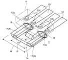
一方、図6および図7は、本発明に係る複数本のコア部17(A,B)を1本の第1溝1a内に配置した、多チャンネルの光モジュールである。なお、図7(b)はコア部17(A,B)とクラッド部18の平面図であるが、クラッド部18の範囲をわかりやすくするために、クラッド部18にハッチングを施している。後述する図11(b)も同様である。 6 and 7 show a multi-channel optical module in which a plurality of core portions 17 (A, B) according to the present invention are arranged in one
複数本(本例では2本)のコア部17(A,B)は、第1基板1の表面の略台形状の第1溝1a内に平行に配置されている。第1溝1aは、複数本のコア部17(A,B)を一定のピッチPで配置できる横幅Wに形成されている。 A plurality (two in this example) of core portions 17 (A, B) are arranged in parallel in a substantially trapezoidal
また、ミラー部15は、各コア部17(A,B)に対応して形成されている。同様に、発光素子12aは、各ミラー部15に対応して実装されている。具体的には、各ミラー部15に対応する2個の発光素子12aを保持するホルダー11が設けられ、このホルダー11の各発光素子12aの回路がバンプ12cでメタル回路(銅や金スパッタによるパターニング回路)10にフリップチップ実装されている。 Moreover, the
そして、隣り合うミラー部15の近傍の第1溝1a内には、ミラー部15の反射光の散乱成分〔図7(a)の矢印aを参照〕が、対応しないコア部17(A)または17(B)に漏洩しないように遮蔽する遮蔽部30が形成されている。 And in the 1st groove |
この遮蔽部30は、隣り合うミラー部15の近傍の間に、第1溝1aを形成しないで、第1基板1を残した、つまり、第1基板1の一部を利用して、第1溝1aの底から上向き隆起状の遮蔽部30としたものである。 This shielding
そして、第1溝1a内に内部導波路16のクラッドを充填して、クラッド部18を形成している。 Then, the clad
前記のような光モジュールは、複数本のコア部17(A,B)を1本の第1溝1a内に配置した、多チャンネルの光モジュールである。そして、ミラー部15の近傍の第1溝1a内に、ミラー部15の反射光の散乱成分aが、対応しないコア部17(A)または17(B)に漏洩しないように遮蔽する遮蔽部30を形成したものである。 The optical module as described above is a multi-channel optical module in which a plurality of core portions 17 (A, B) are arranged in one
したがって、遮蔽部30によって、ミラー部15の反射光の散乱成分aが遮蔽されるようになる。すなわち、図7(a)(b)の例では、コア部17(B)のミラー部15の反射光の散乱成分aが、隣接するチャンネルであるコア部17(A)に漏洩(クロストーク)し難くなる。 Therefore, the scattering component a of the reflected light from the
これにより、データ通信の高速大容量化や双方向通信に対応するための多チャンネル化に対応できるようになる。また、複数本のコア部17(A,B)を1本の第1溝1a内に配置することで、コア部17(A,B)を狭ピッチ化できるので、光モジュールの小型化に寄与できるようになる。なお、図6および図7(以下の図も同様。)では、遮蔽部30の横幅をコア部17(A,B)の横幅よりも広く描いているが、実際には、コア部17(A,B)の横幅よりも狭くできるものである。 As a result, it is possible to cope with an increase in the speed and capacity of data communication and an increase in the number of channels for supporting bidirectional communication. In addition, since the core portions 17 (A, B) can be narrowed by arranging a plurality of core portions 17 (A, B) in one
この遮蔽部30は、ミラー部15の近傍から内部導波路16に沿って、さらに光ファイバー2の方向に適当な長さで延伸させれば〔図7(b)の矢印cを参照〕、コア部17(A,B)の直線部分からの漏洩も抑制できるようになる。 If the shielding
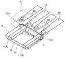
さらに、遮蔽部30は、隣り合うコア部17(A,B)の第1溝1a内に残された第1基板1の一部で形成したものである。そして、第1基板1がシリコン基板であれば、エッチング加工によって、平滑で高精度なミラー部15と、隆起状の遮蔽部30を有する第1溝1aとが同時にかつ容易に形成できるようになる。 Furthermore, the shielding
因みに、図6に対応する図10と、図7に対応する図11に示す光モジュールは、比較のために示した、遮蔽部30の無いタイプをある。このタイプによれば、ミラー部15の反射光の散乱成分aが遮蔽されないので、図11(a)(b)の例では、コア部17(B)のミラー部15の反射光の散乱成分aが、隣接するチャンネルであるコア部17(A)に漏洩(クロストーク)することが分かる。 Incidentally, the optical module shown in FIG. 10 corresponding to FIG. 6 and FIG. 11 corresponding to FIG. 7 is the type without the shielding
図8(a)は、第1基板1の隆起状の遮蔽部30の表面に、第1溝1aの表面も含めて酸化膜層34を形成したものである。なお、酸化膜層34は、ミラー部15の近傍の遮蔽部30の表面だけに限られず、第1基板1の表面全体に形成してもよい。 FIG. 8A shows an
これによれば、酸化膜層34が反射層となるので、散乱成分aの漏洩をより抑制できるようになる。また、コア部17(A,B)の屈折率を遮蔽部30である酸化膜層の屈折率よりも高くすることで、酸化膜層34を下部クラッドとすることができる。 According to this, since the
図8(b)は、図8(a)の隆起状の遮蔽部30の表面に、酸化膜層34の除去部分32を形成したものである。 FIG. 8B shows a structure in which the removed
これによれば、ホルダー11(発光素子12a)とクラッド部18を多重反射する漏洩光dが発生した場合、この漏洩光dを酸化膜層34の除去部分32から第1基板1に吸収させることができる。 According to this, when the leaked light d that multi-reflects the holder 11 (
図9は、第1基板1の隆起状の遮蔽部30の表面に、この遮蔽部30に沿った光吸収体35を配置したものである。光吸収体35としては、例えば不透光性のアクリル若しくはエポキシ樹脂がある。 In FIG. 9, a
これによれば、発光素子12aとクラッド部18を多重反射する漏洩光dが発生した場合、この漏洩光dを光吸収体35で吸収させることができる。 According to this, when the leaked light d that multi-reflects the
前記実施形態では、第1基板1の一部を利用して、第1溝1aの底から上向き隆起状の遮蔽部30としたものであったが、これに限らない。例えば、隣り合うコア部17(A,B)の間に、別の遮蔽シート等を介在させた遮蔽部であってもよい。 In the above-described embodiment, a part of the
以上のように、本発明に係る光モジュールは、基板の表面に形成された溝内に設けられた内部導波路と、この溝の先端部に形成された光路変換用のミラー部と、このミラー部と対向するように基板の表面に実装され、ミラー部を介して内部導波路のコア部に光信号を発光し、若しくはミラー部を介して内部導波路のコア部からの光信号を受光する光素子と、内部導波路のコア部と光学的に結合されるファイバーコア部を有する光ファイバーを備えた光モジュールにおいて、前記コア部は、前記溝内に複数本が平行に配置され、前記溝は、複数本のコア部を一定のピッチで配置できる横幅に形成され、前記ミラー部は、各コア部に対応して形成され、前記光素子は、各ミラー部に対応して実装され、前記溝内には、内部導波路のクラッドが充填されていて、前記ミラー部の近傍の溝内に、ミラー部の反射光の散乱成分が、対応しないコア部に漏洩しないように遮蔽する遮蔽部が形成され、前記遮蔽部は、前記隣り合うコア部の溝内に残された基板の一部で形成され、前記基板は、シリコン基板であることを特徴とするものである。As described above, the optical module according to the present invention includes the internal waveguide provided in the groove formed on the surface of the substrate, the optical path conversion mirror formed at the tip of the groove, and the mirror. Mounted on the surface of the substrate so as to face the part, emits an optical signal to the core part of the internal waveguide via the mirror part, or receives an optical signal from the core part of the internal waveguide via the mirror part In an optical module including an optical element and an optical fiber having a fiber core portion optically coupled to a core portion of an internal waveguide, a plurality of the core portions are arranged in parallel in the groove, A plurality of core parts are formed in a width that can be arranged at a constant pitch, the mirror part is formed corresponding to each core part, the optical element is mounted corresponding to each mirror part, and the groove Inside is filled with cladding of internal waveguide Have been thecore in the groove in the vicinity of the mirror portion, the scattering component of the reflected light of the mirror portion is shielded section for shielding so as not to be leaked to the core portion not corresponding isformed, the shielding portion, wherein the adjacent A part of the substrate left in the groove of the part is formed, and the substrate is a silicon substrate .
これによれば、複数本のコア部を1本の溝内に配置した、多チャンネルの光モジュールにおいて、ミラー部の近傍の溝内に、ミラー部の反射光の散乱成分が、対応しないコア部に漏洩しないように遮蔽する遮蔽部を形成したものである。したがって、遮蔽部によって、ミラー部の反射光の散乱成分が、対応しないコア部、つまり隣接するチャンネルに漏洩(クロストーク)し難くなる。これにより、データ通信の高速大容量化や双方向通信に対応するための多チャンネル化に対応できるようになる。また、複数本のコア部を1本の溝内に配置することで、コア部を狭ピッチ化できるので、光モジュールの小型化に寄与できるようになる。
また、遮蔽部は、隣り合うコア部の溝内に残された基板の一部で形成され、基板がシリコン基板であるから、エッチング加工によって、平滑で高精度なミラー部と、隆起状の遮蔽部を有する溝とが同時にかつ容易に形成できるようになる。According to this, in a multi-channel optical module in which a plurality of core parts are arranged in one groove, the core part to which the reflected light scattering component of the mirror part does not correspond in the groove near the mirror part The shielding part which shields so that it may not leak is formed. Therefore, the shielding component makes it difficult for the scattered component of the reflected light from the mirror portion to leak (crosstalk) to the incompatible core portion, that is, the adjacent channel. As a result, it is possible to cope with an increase in the speed and capacity of data communication and an increase in the number of channels for supporting bidirectional communication. In addition, by arranging a plurality of core portions in one groove, the pitch of the core portions can be reduced, so that the optical module can be miniaturized.
In addition, the shielding part is formed by a part of the substrate left in the groove of the adjacent core part, and the substrate is a silicon substrate. Therefore, a smooth and high-precision mirror part and a raised shielding are obtained by etching. A groove having a portion can be formed simultaneously and easily.
また、前記遮蔽部は、前記ミラー部の近傍から内部導波路に沿って、さらに光ファイバーの方向に延伸されている構成とすることができる。 Moreover, the said shielding part can be set as the structure extended | stretched further in the direction of the optical fiber along the internal waveguide from the vicinity of the said mirror part.
これによれば、コア部の直線部分からの漏洩も抑制できるようになる。 According to this, the leakage from the straight part of the core part can also be suppressed.
また、前記遮蔽部の表面には、前記溝の表面も含めて酸化膜層が形成されている構成とすることができる。 In addition, an oxide film layer may be formed on the surface of the shielding portion including the surface of the groove.
これによれば、酸化膜層が反射層となるので、散乱成分の漏洩をより抑制できるようになる。また、コア部の屈折率を酸化膜層の屈折率よりも高くすることで、酸化膜層を下部クラッドとすることができる。 According to this, since the oxide film layer becomes the reflective layer, the leakage of the scattering component can be further suppressed. Further, by making the refractive index of the core portion higher than the refractive index of the oxide film layer, the oxide film layer can be a lower clad.
また、前記遮蔽部の表面に、酸化膜層の除去部分が形成されている構成とすることができる。 Moreover, it can be set as the structure by which the removal part of the oxide film layer is formed in the surface of the said shielding part.
これによれば、光素子とクラッド部を多重反射する漏洩光が発生した場合、この漏洩光を酸化膜層の除去部分から基板に吸収させることができる。 According to this, in the case where leakage light that multi-reflects the optical element and the clad portion is generated, this leakage light can be absorbed by the substrate from the removed portion of the oxide film layer.
また、前記遮蔽部の表面に、この遮蔽部に沿った光吸収体が配置されている構成とすることができる。 Moreover, it can be set as the structure by which the light absorber along this shielding part is arrange | positioned on the surface of the said shielding part.
これによれば、光素子とクラッドを多重反射する漏洩光が発生した場合、この漏洩光を光吸収体で吸収させることができる。 According to this, in the case where leakage light that multi-reflects the optical element and the clad is generated, this leakage light can be absorbed by the light absorber.
1 第1基板
1a 第1溝
2 光ファイバー
12a 発光素子(光素子)
15 ミラー部
16 内部導波路
17(A,B) コア部
18 クラッド部
21 ファイバーコア部
30 遮蔽部
32 除去部分
34 酸化膜層
35 光吸収体
a,d 散乱成分
P ピッチ
W 横幅DESCRIPTION OF
15
Claims (5)
Translated fromJapanese前記コア部は、前記溝内に複数本が平行に配置され、前記溝は、複数本のコア部を一定のピッチで配置できる横幅に形成され、前記ミラー部は、各コア部に対応して形成され、前記光素子は、各ミラー部に対応して実装され、前記溝内には、内部導波路のクラッドが充填されていて、
前記ミラー部の近傍の溝内に、ミラー部の反射光の散乱成分が、対応しないコア部に漏洩しないように遮蔽する遮蔽部が設けられ、
前記遮蔽部は、前記隣り合うコア部の溝内に残された基板の一部で形成され、前記基板は、シリコン基板であることを特徴とする光モジュール。An internal waveguide provided in a groove formed on the surface of the substrate, an optical path conversion mirror formed at the tip of the groove, and mounted on the surface of the substrate so as to face the mirror, An optical element that emits an optical signal to the core part of the internal waveguide through the mirror part or receives an optical signal from the core part of the internal waveguide through the mirror part, and the optical part and the optical part of the internal waveguide In an optical module comprising an optical fiber having a fiber core portion coupled to
A plurality of the core parts are arranged in parallel in the groove, the groove is formed in a width that allows a plurality of core parts to be arranged at a constant pitch, and the mirror part corresponds to each core part. Formed, the optical element is mounted corresponding to each mirror portion, the groove is filled with a clad of an internal waveguide,
In the groove in the vicinity of the mirror part, a shielding part that shields the scattered component of the reflected light of the mirror part from leaking to the non-corresponding core part is provided,
The optical module is characterized in that theshielding part is formed by a part of a substrate left in the groove of the adjacent core part, and the substrate is a silicon substrate .
Priority Applications (1)
| Application Number | Priority Date | Filing Date | Title |
|---|---|---|---|
| JP2010243924AJP5654316B2 (en) | 2010-10-29 | 2010-10-29 | Optical module |
Applications Claiming Priority (1)
| Application Number | Priority Date | Filing Date | Title |
|---|---|---|---|
| JP2010243924AJP5654316B2 (en) | 2010-10-29 | 2010-10-29 | Optical module |
Publications (2)
| Publication Number | Publication Date |
|---|---|
| JP2012098361A JP2012098361A (en) | 2012-05-24 |
| JP5654316B2true JP5654316B2 (en) | 2015-01-14 |
Family
ID=46390372
Family Applications (1)
| Application Number | Title | Priority Date | Filing Date |
|---|---|---|---|
| JP2010243924AActiveJP5654316B2 (en) | 2010-10-29 | 2010-10-29 | Optical module |
Country Status (1)
| Country | Link |
|---|---|
| JP (1) | JP5654316B2 (en) |
Families Citing this family (1)
| Publication number | Priority date | Publication date | Assignee | Title |
|---|---|---|---|---|
| JP6863909B2 (en)* | 2018-01-18 | 2021-04-21 | 日本電信電話株式会社 | Nanowire optical device |
Family Cites Families (11)
| Publication number | Priority date | Publication date | Assignee | Title |
|---|---|---|---|---|
| GB9203128D0 (en)* | 1992-02-14 | 1992-04-01 | Lucas Ind Plc | Alignment device for optical fibre |
| JP2002182051A (en)* | 2000-10-04 | 2002-06-26 | Sumitomo Electric Ind Ltd | Optical waveguide module |
| JP2003287636A (en)* | 2002-03-28 | 2003-10-10 | Nec Corp | Optical function device and method for manufacturing the same |
| JP2004118117A (en)* | 2002-09-27 | 2004-04-15 | Toshiba Corp | Optical waveguide array film |
| JP4118747B2 (en)* | 2003-05-30 | 2008-07-16 | 株式会社フジクラ | Optical module, optical transceiver system |
| JP4125180B2 (en)* | 2003-05-30 | 2008-07-30 | 株式会社フジクラ | Optical module, optical module manufacturing method, and optical transmission / reception system |
| JP2006084889A (en)* | 2004-09-17 | 2006-03-30 | Fujikura Ltd | Optical connection device |
| JP4882644B2 (en)* | 2006-08-10 | 2012-02-22 | パナソニック電工株式会社 | Photoelectric conversion device |
| JP2008129385A (en)* | 2006-11-22 | 2008-06-05 | Shinko Electric Ind Co Ltd | Optical component mounting substrate and optical module |
| JP2009008769A (en)* | 2007-06-26 | 2009-01-15 | Panasonic Electric Works Co Ltd | Manufacturing method of photoelectric conversion device |
| JP4577376B2 (en)* | 2008-02-21 | 2010-11-10 | ソニー株式会社 | Manufacturing method of optical waveguide |
- 2010
- 2010-10-29JPJP2010243924Apatent/JP5654316B2/enactiveActive
Also Published As
| Publication number | Publication date |
|---|---|
| JP2012098361A (en) | 2012-05-24 |
Similar Documents
| Publication | Publication Date | Title |
|---|---|---|
| JP5690324B2 (en) | Optical module | |
| JP5664905B2 (en) | Photoelectric conversion module | |
| JP5919573B2 (en) | Optical module | |
| US9046668B2 (en) | Optical module | |
| CN103250471B (en) | Printed circuit board assembly and method for manufacturing the same | |
| JP6590161B2 (en) | Manufacturing method of active optical cable | |
| JP2017090909A (en) | Photoelectric conversion assembly | |
| USRE46633E1 (en) | Optical module | |
| EP2390699A1 (en) | Optical coupler module having optical waveguide structure | |
| JP2010197817A (en) | Optical connector | |
| JPWO2014034458A1 (en) | Connection structure between optical module and optical connector | |
| JP6728639B2 (en) | Optical wiring connection structure and optical wiring connection method | |
| JP5654317B2 (en) | Optical module | |
| JP5395042B2 (en) | Manufacturing method of optical path conversion device | |
| JP2013057720A (en) | Optical module | |
| JP2017198778A (en) | Optical wiring packaging structure, optical module, and electronic apparatus | |
| JP5654316B2 (en) | Optical module | |
| JP5879541B2 (en) | Optical module | |
| JP5647485B2 (en) | Optical module | |
| JP2013003549A (en) | Optical module | |
| JP2012069882A (en) | Optical module | |
| KR100864962B1 (en) | Flexible Optical Connection Module for Flat Panel Display and Manufacturing Method Thereof | |
| JP2009223340A (en) | Optical component and optical path changing device used for the same | |
| JP5654847B2 (en) | Optical module | |
| JP2015222291A (en) | Substrate structure and optical module substrate |
Legal Events
| Date | Code | Title | Description |
|---|---|---|---|
| A621 | Written request for application examination | Free format text:JAPANESE INTERMEDIATE CODE: A621 Effective date:20130805 | |
| A977 | Report on retrieval | Free format text:JAPANESE INTERMEDIATE CODE: A971007 Effective date:20140226 | |
| A131 | Notification of reasons for refusal | Free format text:JAPANESE INTERMEDIATE CODE: A131 Effective date:20140304 | |
| A521 | Written amendment | Free format text:JAPANESE INTERMEDIATE CODE: A523 Effective date:20140403 | |
| A711 | Notification of change in applicant | Free format text:JAPANESE INTERMEDIATE CODE: A711 Effective date:20141009 | |
| RD03 | Notification of appointment of power of attorney | Free format text:JAPANESE INTERMEDIATE CODE: A7423 Effective date:20141015 | |
| TRDD | Decision of grant or rejection written | ||
| A01 | Written decision to grant a patent or to grant a registration (utility model) | Free format text:JAPANESE INTERMEDIATE CODE: A01 Effective date:20141111 | |
| A61 | First payment of annual fees (during grant procedure) | Free format text:JAPANESE INTERMEDIATE CODE: A61 Effective date:20141120 | |
| R150 | Certificate of patent or registration of utility model | Ref document number:5654316 Country of ref document:JP Free format text:JAPANESE INTERMEDIATE CODE: R150 |