JP5647864B2 - Touch panel - Google Patents
Touch panelDownload PDFInfo
- Publication number
- JP5647864B2 JP5647864B2JP2010249208AJP2010249208AJP5647864B2JP 5647864 B2JP5647864 B2JP 5647864B2JP 2010249208 AJP2010249208 AJP 2010249208AJP 2010249208 AJP2010249208 AJP 2010249208AJP 5647864 B2JP5647864 B2JP 5647864B2
- Authority
- JP
- Japan
- Prior art keywords
- electrode
- touch panel
- band
- conductive
- direction parallel
- Prior art date
- Legal status (The legal status is an assumption and is not a legal conclusion. Google has not performed a legal analysis and makes no representation as to the accuracy of the status listed.)
- Active
Links
Images


Classifications
- G—PHYSICS
- G06—COMPUTING OR CALCULATING; COUNTING
- G06F—ELECTRIC DIGITAL DATA PROCESSING
- G06F3/00—Input arrangements for transferring data to be processed into a form capable of being handled by the computer; Output arrangements for transferring data from processing unit to output unit, e.g. interface arrangements
- G06F3/01—Input arrangements or combined input and output arrangements for interaction between user and computer
- G06F3/03—Arrangements for converting the position or the displacement of a member into a coded form
- G06F3/041—Digitisers, e.g. for touch screens or touch pads, characterised by the transducing means
- G06F3/044—Digitisers, e.g. for touch screens or touch pads, characterised by the transducing means by capacitive means
- G06F3/0445—Digitisers, e.g. for touch screens or touch pads, characterised by the transducing means by capacitive means using two or more layers of sensing electrodes, e.g. using two layers of electrodes separated by a dielectric layer
- H—ELECTRICITY
- H05—ELECTRIC TECHNIQUES NOT OTHERWISE PROVIDED FOR
- H05K—PRINTED CIRCUITS; CASINGS OR CONSTRUCTIONAL DETAILS OF ELECTRIC APPARATUS; MANUFACTURE OF ASSEMBLAGES OF ELECTRICAL COMPONENTS
- H05K7/00—Constructional details common to different types of electric apparatus
- H05K7/02—Arrangements of circuit components or wiring on supporting structure
- G—PHYSICS
- G06—COMPUTING OR CALCULATING; COUNTING
- G06F—ELECTRIC DIGITAL DATA PROCESSING
- G06F3/00—Input arrangements for transferring data to be processed into a form capable of being handled by the computer; Output arrangements for transferring data from processing unit to output unit, e.g. interface arrangements
- G06F3/01—Input arrangements or combined input and output arrangements for interaction between user and computer
- G06F3/03—Arrangements for converting the position or the displacement of a member into a coded form
- G06F3/041—Digitisers, e.g. for touch screens or touch pads, characterised by the transducing means
- G06F3/0412—Digitisers structurally integrated in a display
- G—PHYSICS
- G06—COMPUTING OR CALCULATING; COUNTING
- G06F—ELECTRIC DIGITAL DATA PROCESSING
- G06F3/00—Input arrangements for transferring data to be processed into a form capable of being handled by the computer; Output arrangements for transferring data from processing unit to output unit, e.g. interface arrangements
- G06F3/01—Input arrangements or combined input and output arrangements for interaction between user and computer
- G06F3/03—Arrangements for converting the position or the displacement of a member into a coded form
- G06F3/041—Digitisers, e.g. for touch screens or touch pads, characterised by the transducing means
- G06F3/045—Digitisers, e.g. for touch screens or touch pads, characterised by the transducing means using resistive elements, e.g. a single continuous surface or two parallel surfaces put in contact
- G—PHYSICS
- G06—COMPUTING OR CALCULATING; COUNTING
- G06F—ELECTRIC DIGITAL DATA PROCESSING
- G06F2203/00—Indexing scheme relating to G06F3/00 - G06F3/048
- G06F2203/041—Indexing scheme relating to G06F3/041 - G06F3/045
- G06F2203/04103—Manufacturing, i.e. details related to manufacturing processes specially suited for touch sensitive devices
- G—PHYSICS
- G06—COMPUTING OR CALCULATING; COUNTING
- G06F—ELECTRIC DIGITAL DATA PROCESSING
- G06F2203/00—Indexing scheme relating to G06F3/00 - G06F3/048
- G06F2203/041—Indexing scheme relating to G06F3/041 - G06F3/045
- G06F2203/04104—Multi-touch detection in digitiser, i.e. details about the simultaneous detection of a plurality of touching locations, e.g. multiple fingers or pen and finger
- G—PHYSICS
- G06—COMPUTING OR CALCULATING; COUNTING
- G06F—ELECTRIC DIGITAL DATA PROCESSING
- G06F2203/00—Indexing scheme relating to G06F3/00 - G06F3/048
- G06F2203/041—Indexing scheme relating to G06F3/041 - G06F3/045
- G06F2203/04112—Electrode mesh in capacitive digitiser: electrode for touch sensing is formed of a mesh of very fine, normally metallic, interconnected lines that are almost invisible to see. This provides a quite large but transparent electrode surface, without need for ITO or similar transparent conductive material
Landscapes
- Engineering & Computer Science (AREA)
- General Engineering & Computer Science (AREA)
- Theoretical Computer Science (AREA)
- Human Computer Interaction (AREA)
- Physics & Mathematics (AREA)
- General Physics & Mathematics (AREA)
- Microelectronics & Electronic Packaging (AREA)
- Position Input By Displaying (AREA)
Description
Translated fromJapanese本発明は、タッチパネル(タッチスクリーン)に関する。特に、異なる2層にそれぞれ、細線パターンによる電極列が形成されたマルチタッチ可能な静電容量方式、あるいは抵抗膜方式のタッチパネルに関する。 The present invention relates to a touch panel (touch screen). In particular, the present invention relates to a multi-touch capable capacitive type or resistive film type touch panel in which electrode rows having thin line patterns are formed on two different layers.
タッチパネルには、ドットスペーサーを介在させて対向配置した2つの導電膜(電極層)間のタッチ位置での導通を検知するアナログ抵抗膜方式が多く用いられてきたが(例えば、特許文献1)、近年、静電容量の変化を利用して指先のタッチ位置を検出する静電容量方式のタッチパネルの開発が進められている。静電容量方式のタッチパネルには、表面型と投影型とがある。表面型は、1シート状の電極を有する。電極材料には以前からITOなどの透明導電膜が用いられてきたが、ITOの抵抗値が高いため、応答性の観点から、大画面化が難しい。このため、金、銀、銅などの金属細線を電極に用いる技術の開発が進められている(特許文献2)。ところで、表面型タッチパネルは、例えば、指と導電膜との間の静電容量の変化に応じた導電膜のアナログ電流変化量をシート四隅の電極で検出する構成とされるので、同時に2点以上の接触(マルチタッチ)を検出することが難しい。
一方、投影型タッチパネルは、配列方向が第一方向である第一電極列と、配列方向が第一方向と直交する第二方向である第二電極列とが誘電層を介在して直交配置された格子状の電極を有する(特許文献3)。この投影型では、タッチ時の容量結合に起因する第一電極列と第二電極列との間の静電容量の変化を電圧変化として検出して座標点を特定することにより、複数のタッチ位置を検出可能である。For the touch panel, an analog resistance film method for detecting conduction at a touch position between two conductive films (electrode layers) arranged to face each other with a dot spacer interposed therebetween (for example, Patent Document 1) has been used. In recent years, development of a capacitive touch panel that detects the touch position of a fingertip using a change in capacitance has been advanced. Capacitive touch panels include a surface type and a projection type. The surface type has one sheet-like electrode. As the electrode material, a transparent conductive film such as ITO has been used for some time. However, since the resistance value of ITO is high, it is difficult to enlarge the screen from the viewpoint of responsiveness. For this reason, development of a technique using metal fine wires such as gold, silver, and copper as an electrode is underway (Patent Document 2). By the way, the surface-type touch panel is configured to detect, for example, the amount of change in analog current of the conductive film according to the change in capacitance between the finger and the conductive film with the electrodes at the four corners of the sheet. It is difficult to detect contact (multi-touch).
On the other hand, in the projection type touch panel, the first electrode array whose arrangement direction is the first direction and the second electrode array whose arrangement direction is the second direction orthogonal to the first direction are arranged orthogonally with a dielectric layer interposed therebetween. A grid-like electrode (Patent Document 3). In this projection type, a plurality of touch positions are determined by detecting a change in capacitance between the first electrode row and the second electrode row due to capacitive coupling at the time of touching as a voltage change and identifying coordinate points. Can be detected.
近年、マルチタッチ及び大画面化に対する要望が高まっている。これらの要望に対しては、2つの電極層を有する投影型を採用し、金属細線を用いて電極を形成することが好ましいが、二方向の電極列が互いに直交するように重ねられる構造上、金属細線の製造と、電極列を重ね合わせる際の位置決め等には注意を要する。すなわち、金属細線により電極を形成する場合、例えば、一定間隔で互いに平行に延びる多数の平行線と、これに交差する交差線とによって電極列が形成されるが、重ね合わせの際の僅かな誤差や、金属細線の形状誤差等により、一方の電極列の金属細線と他方の電極列の金属細線との配置関係が乱れる可能性がある。このとき、金属細線同士が互いに近接してその部分が太く見えてしまうこと(線太り)や、光干渉による干渉縞(モアレ)が生じ易い。近年、携帯電子機器などにも解像度の高いディスプレイが搭載されることが多くなってきたが、このようなディスプレイの高精細な画像上の互いに近接する点と点とを判別可能な感度を得るため、金属細線の間隔を狭くした場合には、線太りや干渉縞が特に起こり易い。このような線太り及び干渉縞の生じた部分が視認されてしまうことにより、ディスプレイの表示品位が低下するおそれがあるため、パターン形成及び重ね合わせに対して非常に高精度が要求され、歩留まり低下及びコストアップに繋がってしまう。
なお、抵抗膜方式においても、2つの電極層をそれぞれ金属細線で形成することが考えられる。この場合2つの電極層を重ね合わせる際に線太りやモアレが生じ易いことは投影型静電容量方式の場合と同様であるため、抵抗膜方式においても上記と同様の課題がある。In recent years, there has been an increasing demand for multi-touch and a large screen. For these demands, it is preferable to adopt a projection type having two electrode layers and to form electrodes using fine metal wires, but on the structure in which two-direction electrode rows are stacked so as to be orthogonal to each other, Care must be taken in the production of fine metal wires and positioning when the electrode rows are overlapped. That is, when an electrode is formed by a thin metal wire, for example, an electrode row is formed by a large number of parallel lines extending parallel to each other at regular intervals and intersecting lines intersecting with each other. In addition, there is a possibility that the arrangement relationship between the fine metal wire of one electrode row and the fine metal wire of the other electrode row is disturbed due to a shape error of the fine metal wire. At this time, the metal thin wires are close to each other and the portion looks thick (line thickening), and interference fringes (moire) due to optical interference are likely to occur. In recent years, high-resolution displays have often been mounted on portable electronic devices and the like, but in order to obtain a sensitivity that can distinguish points that are close to each other on a high-definition image of such displays. When the interval between the thin metal wires is narrowed, line thickening and interference fringes are particularly likely to occur. Since the display quality of the display may be deteriorated due to the visual recognition of the portion where such line thickening and interference fringes are generated, very high accuracy is required for pattern formation and superposition, and the yield decreases. And this leads to an increase in cost.
In the resistive film method, it is conceivable to form the two electrode layers with fine metal wires, respectively. In this case, the fact that line thickening and moire are likely to occur when the two electrode layers are overlaid is the same as in the case of the projection-type electrostatic capacitance method.
本発明の目的は、金属細線などの細線を用いて容易に製造可能な投影型静電方式タッチパネルを提供することにある。 An object of the present invention is to provide a projected electrostatic touch panel that can be easily manufactured using thin wires such as metal thin wires.
第一方向と、前記第一方向に交差する第二方向とのうち第二方向に沿って互いに平行に延びる複数の導線が配置された第二方向平行帯が前記第一方向の第一方向間隙を挟んで前記第一方向に繰り返し形成され、かつ前記第一方向に沿って延びて前記第二方向平行帯に交差する導線が配置された第一方向交差帯が前記第二方向に繰り返し形成された第一電極と、
前記第一方向に沿って互いに平行に延びる複数の導線が配置された第一方向平行帯が前記第二方向の第二方向間隙を挟んで前記第二方向に繰り返し形成され、かつ前記第二方向に沿って延びて前記第一方向平行帯に交差する導線が配置された第二方向交差帯が前記第一方向に繰り返し形成された第二電極と、を備え、
前記第一電極において前記第一方向間隙には導線が配置されておらず、かつ前記第二電極において前記第二方向間隙には導線が配置されておらず、
前記第一方向間隙の位置に前記第二方向交差帯が対応し、前記第二方向間隙の位置に前記第一方向交差帯が対応するように、前記第一電極と前記第二電極とが互いに重ねられることを特徴とするタッチパネル。The first direction gap in the first direction is a second direction parallel band in which a plurality of conductive wires extending in parallel with each other along the second direction are arranged among the first direction and the second direction intersecting the first direction. A first direction crossing band is repeatedly formed in the second direction. The first direction crossing band is disposed in the first direction with the conductors extending along the first direction and intersecting the second direction parallel band. The first electrode,
A first-direction parallel strip in which a plurality of conductive wires extending in parallel with each other along the first direction is repeatedly formed in the second direction across the second-direction gap in the second direction, and the second direction A second electrode in which a second direction crossing band in which a conductive wire extending along the first direction parallel band is arranged is repeatedly formed in the first direction, and
No conducting wire is arranged in the first direction gap in the first electrode, and no conducting wire is arranged in the second direction gap in the second electrode,
The first electrode and the second electrode are mutually connected so that the second direction crossing band corresponds to the position of the first direction gap and the first direction crossing band corresponds to the position of the second direction gap. A touch panel characterized by being overlaid.
本発明のタッチパネルによれば、第一電極と第二電極とを重ね合わせる際の誤差や、導線の形状誤差に対する許容度が大きく、重ね合わせが少々ずれていたり導線の形状にバラツキがあったとしても格子形状に違和感を感じない新規な導線パターンが得られる。すなわち、金属細線などの細線を用いて容易に製造可能な静電容量方式や抵抗膜方式の静電容量方式タッチパネルを提供することができる。 According to the touch panel of the present invention, there is a large tolerance for overlapping the first electrode and the second electrode and the shape error of the conductor, and the overlay is slightly shifted or the shape of the conductor is uneven. A new conductor pattern that does not feel uncomfortable in the lattice shape can be obtained. That is, it is possible to provide a capacitive touch panel of a capacitive type or a resistive film type that can be easily manufactured using a thin line such as a thin metal line.
図1〜図9を参照して、本発明の実施形態を説明するための静電容量方式タッチパネルの例について説明する。なお、以下の説明において、既に説明した構成と同様の構成については、同一符号を付し、その説明を省略する。
本明細書において「〜」は、その前後に記載される数値を下限値及び上限値として含む意味で使用される。With reference to FIGS. 1-9, the example of the capacitive touch panel for demonstrating embodiment of this invention is demonstrated. In the following description, components similar to those already described are given the same reference numerals and description thereof is omitted.
In the present specification, “to” is used in the sense of including the numerical values described before and after it as lower and upper limits.
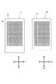
図1(A)〜(C)はそれぞれ、本発明の投影型静電容量方式タッチパネルの一例の断面図を模式的に示す。タッチパネル1〜3はいずれも、複数の層の積層体であり、指先によってタッチされる側に配置される第一電極としての上部電極20と、この上部電極20に重ねられて、画像表示装置としてのディスプレイ9(図9)側に配置される第二電極としての下部電極40とを備える。図1(A)〜(C)のそれぞれの構成では、積層体における上部電極20及び下部電極40の配置位置が相違する。なお、タッチパネル1〜3はディスプレイに一体に形成されていてもよい。 1A to 1C each schematically show a cross-sectional view of an example of a projected capacitive touch panel according to the present invention. Each of the
図1(A)では、上部電極20が形成された上部透明基板11と、下部電極40が形成された下部透明基板12とが、透明な誘電層13を介して電極形成面を向かい合わせに重ねられた状態で貼り合わせられている。上部透明基板12には、ガラス製又は樹脂製の透明カバー部材15が粘着層14を介して設けられる。
図1(B)では、1枚の透明基板11の表面に、下部電極40が形成され、その上に、誘電層13を介して上部電極20が形成されている。
図1(C)では、誘電層としての1枚の透明基板11の表裏両面にそれぞれ、上部電極20と下部電極40とが形成されている。
なお、図1(A)〜(C)には図示していないが、タッチパネル1〜3のディスプレイ9との対向面に、ディスプレイからの電磁波を遮蔽するシールド層が設けられていてもよい。In FIG. 1A, the upper
In FIG. 1B, a
In FIG. 1C, an
Although not illustrated in FIGS. 1A to 1C, a shield layer that shields electromagnetic waves from the display may be provided on the surface of the
上記のタッチパネル1〜3に関し、透明カバー部材15、透明基板11、透明基板12、及びシールド層には、絶縁性の同じ材料を用いてもよいし、絶縁性のそれぞれ別々の材料を用いてもよく、プラスチックフィルム、プラスチック板、ガラス板等が使用されて形成される。これらの部材、板、層の厚みはそれぞれの用途に応じて適宜決められる。 Regarding the
上記プラスチックフィルム及びプラスチック板の材料としては、例えば、ポリエチレンテレフタレート(PET)、ポリエチレンナフタレート(PEN)等のポリエステル類;ポリエチレン(PE)、ポリプロピレン(PP)、ポリスチレン、EVA等のポリオレフィン類;ビニル系樹脂;その他、ポリカーボネート(PC)、ポリアミド、ポリイミド、アクリル樹脂、トリアセチルセルロース(TAC)等が用いられる。 Examples of the material of the plastic film and the plastic plate include polyesters such as polyethylene terephthalate (PET) and polyethylene naphthalate (PEN); polyolefins such as polyethylene (PE), polypropylene (PP), polystyrene, and EVA; Resin; In addition, polycarbonate (PC), polyamide, polyimide, acrylic resin, triacetyl cellulose (TAC) and the like are used.
上記プラスチックフィルム及びプラスチック板の好ましい材料としては、PET(融点:258℃)、PEN(融点:269℃)、PE(融点:135℃)、PP(融点:163℃)、ポリスチレン(融点:230℃)、ポリ塩化ビニル(融点:180℃)、ポリ塩化ビニリデン(融点:212℃)やTAC(融点:290℃)等の融点が約290℃以下であるプラスチックフィルム、又はプラスチック板などがあり、特に、光透過性や加工性等の観点から、PETが好ましい。フィルムや板の厚みは50μmから300μmであることが好ましい。 Preferred materials for the plastic film and plastic plate include PET (melting point: 258 ° C.), PEN (melting point: 269 ° C.), PE (melting point: 135 ° C.), PP (melting point: 163 ° C.), polystyrene (melting point: 230 ° C.). ), Polyvinyl chloride (melting point: 180 ° C.), polyvinylidene chloride (melting point: 212 ° C.), TAC (melting point: 290 ° C.), etc. From the viewpoints of light transmittance and processability, PET is preferred. The thickness of the film or plate is preferably 50 μm to 300 μm.
誘電層13は、その全体が粘着性を有する材料により非導電性の粘着層として形成されるか、あるいは誘電性の基板と、この基板の表裏にそれぞれ設けられる粘着層とを含んで構成される。このような誘電層13に含まれる粘着層と、透明カバー部材15に設けられる粘着層14とには、非導電性の接着剤などを用いることができる。接着剤の材料としては、アクリル樹脂系、エポキシ樹脂系、フェノール樹脂系、ビニル樹脂系などを例示できる。これらの粘着層は、例えば、スクリーン印刷法などによって形成される。 The
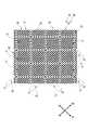
図2は、上部電極20の部分拡大平面図である。図2の状態では、上部電極20が有する第一電極列が形成されていない。ここで、図2〜図8は、導線パターンの構成を模式的に示しており、特に導線の幅を導線間のピッチに対して太く強調して示すものである。後述する種々の電極の部分拡大平面図についても同様である。複数の導線のそれぞれの幅、間隔、断線長さなどは、適宜決められる。
上部電極20が形成される透明基板には、多数の導線(金属細線とも言う)が形成されている。具体的に、透明基板には、第一方向D1と、これに交差する(ここでは略直交し、直交はしていない)第二方向D2とのうち第二方向D2に沿って平行に延びる複数の導線220を含む第二方向平行帯22と、第二方向平行帯22に交差する導線210を含む第一方向交差帯21とが形成されている。FIG. 2 is a partially enlarged plan view of the
A large number of conducting wires (also referred to as metal thin wires) are formed on the transparent substrate on which the
第二方向平行帯22は、導線220が等間隔に配置された帯状の領域であり、第一方向間隙S1を介して第一方向に間をおいて、第一方向D1に繰り返し形成されている。図2に示した第一方向間隙S1は、導線220のピッチP1の2倍の寸法に設定されている。このような第二方向平行帯22及び第一方向間隙S1の構成は、見方を変えれば、上部電極20が形成される基板の導線パターン形成領域全体に多数の導線220が等間隔に形成された構成から、所々で導線220を間引いた構成ともいえる。 The second direction
図2の構成では、第一方向交差帯21が占める領域が1本の導線210の形成領域と同一である。ただし、第一方向交差帯に2本以上の導線が含まれていてもよく、この場合の第一方向平行帯は、これら導線を含む帯状の領域に形成される。2本以上の導線により第一方向交差帯が形成される場合には、一部の導線が焼損しても他の導線によって、後述する電極列の導通が確保されるので良い。第一方向交差帯21の導線210は、第二方向D2に間をおいて、等しいピッチP2で繰り返し形成されている。ピッチP2はピッチP1よりも大きい。ピッチP1は、100μm〜500μmが好ましく、より好ましくは150μm〜400μm、更に好ましくは250μm〜350μmである。
また、ピッチP2は、1000μm〜20000μmが好ましく、より好ましくは2000μm〜10000μm、更に好ましくは3500μm〜7000μmである。すなわち、上記の導線220が密に配置されているとすると、導線210はそれよりも疎の状態に配置されている。In the configuration of FIG. 2, the area occupied by the first
The pitch P2 is preferably 1000 μm to 20000 μm, more preferably 2000 μm to 10000 μm, and still more preferably 3500 μm to 7000 μm. That is, if the above-mentioned
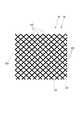
図3は、下部電極40の部分拡大平面図である。この図3の状態では、下部電極40が有する第二電極列が形成されていない。この下部電極40が有する導線は、上述した上部電極20の導線とほぼ同様に配置される。但し、上部電極20の導線パターンと、下部電極40の導線パターンとのそれぞれの方向関係が逆になるように、上部電極20と下部電極40とが重ねられるため、重ねられたときの方向を用いて区別すれば、上部電極20には複数の導線220を含む第二方向平行帯22が形成されるのに対して、下部電極40には複数の導線410を含む第一方向平行帯41が形成されている。また、上部電極20には導線210を含む第一方向交差帯21が形成されるのに対して、下部電極40には導線420を含む第二方向交差帯42が形成される。
第一方向平行帯41は、第二方向間隙S2を介して第二方向D2に間をおいて、第二方向D2に繰り返し形成されている。
ここで、上部電極20の導線パターンと下部電極40の導線パターンとは、図2及び図3の上下方向を綴じ方向としたときに互いに鏡像の関係にある。すなわち、紙面の上下方向に延びる中心線を設定したときに、その中心線に関して線対称に形成されている。FIG. 3 is a partially enlarged plan view of the
The first direction
Here, the conductive pattern of the
導線210,220,410,420としての金属細線の間隔(ピッチ)、線幅、厚さ、本数等の詳細な構成について述べる。
第一方向に延びる導線410(図3)のピッチと、第二方向に延びる導線220(図2)のピッチとは、上記のように同一のピッチP1でなくても、異なっていてもよい。但し、同一のピッチであることが好ましく、異なる場合でも導線410のピッチと導線220のピッチとの寸法比が2倍以内であることが好ましい。
また、金属細線の線幅は細いほど視認され難く、かつ干渉縞が生じにくい。このため、金属細線の線幅は20μm以下であることが好ましく、10μm以下であることがより好ましく、8μm以下であることが更に好ましく、6μm以下であることが特に好ましい。一方、線幅が細いほど加工が難しくコスト高となるため、金属細線の線幅は、1μm以上であることが好ましく、2μm以上であることがより好ましく、4μm以上であることが更に好ましい。
金属細線の厚さ(基板面からの高さ)は、薄い方が基板から剥離しにくいので好ましいが、薄過ぎて細線の断面積が小さくなると、電気抵抗が大きくなって接触検知に必要な静電容量変化量が不足するので応答性が悪くなる。従って、金属細線の厚さは5μm以下が好ましく、0.1μm〜5μmがより好ましく、0.5μm〜3μmが更に好ましい。
金属細線の剥離を防止するためには、金属細線の厚さに対する線幅の比率(線幅/厚さ)を2.5以上にするのが好ましく、4以上にするのが更に好ましい。
また、第一方向平行帯41を構成する導線410及び第二方向平行帯22を構成する導線220のそれぞれの数は3本以上(11本)であり、第一方向交差帯21を構成する導線210及び第二方向交差帯42を構成する導線420のそれぞれの数は1本以上10本以下(1本)であって、第一方向平行帯41を構成する導線410及び第二方向平行帯22を構成する導線220のそれぞれの数(11本)よりも少ない。
なお、金属細線の材料及び製造方法については後述する。A detailed configuration such as an interval (pitch), a line width, a thickness, and the number of thin metal wires as the conducting
The pitch of the conducting wires 410 (FIG. 3) extending in the first direction and the pitch of the conducting wires 220 (FIG. 2) extending in the second direction may not be the same pitch P1 as described above, but may be different. However, it is preferable that the pitches are the same, and even if they are different, it is preferable that the dimensional ratio between the pitch of the
Further, the thinner the metal wire is, the less visible it is and the less likely the interference fringes are produced. For this reason, the line width of the fine metal wires is preferably 20 μm or less, more preferably 10 μm or less, further preferably 8 μm or less, and particularly preferably 6 μm or less. On the other hand, the thinner the line width is, the more difficult the processing becomes and the higher the cost. Therefore, the line width of the fine metal wire is preferably 1 μm or more, more preferably 2 μm or more, and further preferably 4 μm or more.
The thickness of the thin metal wire (height from the substrate surface) is preferable because it is less likely to peel from the substrate. However, if it is too thin and the cross-sectional area of the fine wire is small, the electrical resistance increases and the static electricity necessary for contact detection is required. Responsiveness deteriorates because the amount of change in capacitance is insufficient. Therefore, the thickness of the fine metal wire is preferably 5 μm or less, more preferably 0.1 μm to 5 μm, and still more preferably 0.5 μm to 3 μm.
In order to prevent peeling of the fine metal wires, the ratio of the line width to the thickness of the fine metal wires (line width / thickness) is preferably 2.5 or more, and more preferably 4 or more.
The number of each of the conducting
In addition, the material and manufacturing method of a metal fine wire are mentioned later.
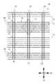
図4は、第一電極列30が形成された状態の上部電極20の部分拡大平面図である。
第一電極列30は、第一方向D1に配列された四角形(閉図形)の複数の電極片31を有する。各電極片31は、上部電極20上に想定した四角形F1の辺(端縁線)に交差する各導線パターン210,220の一部が選択的に断線されることによって形成されている。具体的に、四角形F1の辺に交差する導線210,220のうち、導線220は断線され、導線210は断線されない。四角形F1における一方の対角の頂点はそれぞれ、導線210上において隣り合う二箇所の第一方向間隙S1の位置を通る。複数の導線220が断線されることにより、四角形F1の内部に、複数の導線220が導線210によって互いに導通された一纏まりの領域としての電極片31が区画されるとともに、各電極片31が導線210によって導通した第一電極列30が形成される。第一電極列30は、各導線210毎に形成され、第二方向D2に繰り返し配置される。
なお、導線の断線部は、実際の寸法よりも大きく強調して図示されている。他の図においても同様である。FIG. 4 is a partially enlarged plan view of the
The
In addition, the disconnection part of conducting wire is emphasized and shown larger than an actual dimension. The same applies to the other drawings.
このように複数の導線220が断線されることにより、第一電極列30が形成されるとともに、第一電極列30と第一電極列30との間に、すなわち四角形F1の外側に、他の導線とは導通しておらず電気的に孤立した複数の導線片が形成される。これら一群の導線片をダミー電極35と総称する。すなわち、図4に示した上部電極20の導線パターン形成領域(図4にはその一部を図示)は、断線により、第一電極列30とダミー電極35とに区画される。なお、ダミー電極35は、回路の基準電位(GND)に接地されていてもよい。ダミー電極35の形成により、電極列間の寄生容量が低下するので、隣り合う電極列同士が高周波駆動時に短絡することが防止される。 By disconnecting the plurality of conducting
以下では、断線された導線のそれぞれの部分の集合のことを断線部CLという。つまり、断線部CLは、個々の導線における断線部分をたどった形状とされる。図5は、断線部CLを太い実線で強調して示した上部電極20の平面図である。ここで、断線部CLは、導線の一部を除去することによって形成されていてもよいし、予め、同一線上で間隙をおいて導線パターンを形成する導線のパターニングにより形成されていてもよい。 Hereinafter, a set of respective portions of the disconnected conductor is referred to as a disconnected portion CL. That is, the disconnection portion CL has a shape that follows the disconnection portion of each conductor. FIG. 5 is a plan view of the
断線部CLの形状や寸法などの詳細な構成について述べる。断線部CLのパターンは、同一形状でかつ同一面積とされた多角形の形状であることが好ましく、多角形の中でも正方形あるいは菱形が特に好ましい。
断線部CLの幅(断線長さ)、すなわち断線により分断された結果形成された細線端部と細線端部との間の間隔(断線部CLにおける四角形F1の端縁線に交差する方向の断線寸法)は、10μm以上であることが好ましい。この断線部CLの幅(断線長さ)の上限は特にないが、パターン設計を煩雑にしないためには、金属細線の間隔(ピッチ)長を上限に、断線部CLの幅を決めることが好ましい。A detailed configuration such as the shape and dimensions of the disconnected portion CL will be described. The pattern of the disconnected portion CL is preferably a polygonal shape having the same shape and the same area, and among the polygons, a square or a rhombus is particularly preferable.
The width (disconnection length) of the disconnection portion CL, that is, the interval between the fine wire end portion and the thin wire end portion formed as a result of the disconnection due to the disconnection (disconnection in the direction intersecting the edge line of the rectangle F1 in the disconnection portion CL) The dimension) is preferably 10 μm or more. There is no particular upper limit on the width (disconnection length) of the disconnection portion CL, but in order not to complicate the pattern design, it is preferable to determine the width of the disconnection portion CL with the interval (pitch) length of the fine metal wires as the upper limit. .
図6は、第二電極列50が形成された状態の下部電極40の部分拡大平面図である。第二電極列50は、第二方向D2に配列された四角形の複数の電極片51を有する。各電極片51は、配列方向以外は上述の電極片31と同様に形成される。すなわち、四角形F1の辺に交差する導線410,420のうち導線410は断線され、導線420は断線されない。これにより、各電極片51が導線420によって導通した第二電極列50が形成される。図7は、断線部CLを太い破線で強調して示した第二電極列50の平面図である。 FIG. 6 is a partially enlarged plan view of the
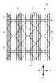
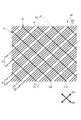
図8は、図4の上部電極20と図6の下部電極40とが重ねられた状態の透視平面図である。上部電極20と下部電極40とは、第一電極列30における電極片31の配列方向(第一方向D1)と、第二電極列50における電極片51の配列方向(第二方向D2)とが略直交するように、誘電層13(図1)を介して重ねられる。このように上部電極20と下部電極40とが重ねられた際に、第一電極列30が下部電極40側のダミー電極35に重なり、第二電極列50が上部電極20側のダミー電極35に重なり、第一電極列30と第二電極列50とは互いに重ならない。すなわち、第一電極列30の電極片31、及び第二電極列50の電極片51は、互いに重ならない状態でぎっしりと第一方向D1及び第二方向D2に配列される。第一方向間隙S1と第二方向間隙S2との交点近傍には、4つの電極片31,31,51,51がそれぞれの角を突き合わせるようにして配置されている。 FIG. 8 is a perspective plan view of the state in which the
第一方向D1と第二方向D2との交差角度と、電極片31,51の形状とは相関しており、これらは適宜決められる。閉図形の形状とされる電極片は、菱形、正方形、矩形などの多角形、あるいは円形、楕円形などの形状であってよい。なお、閉図形は、1本以上の線により区画された閉じた空間をその内部に有する図形をいう。 The intersection angle between the first direction D1 and the second direction D2 correlates with the shapes of the
ここで、上部電極20と下部電極40とが重ねられた状態では、上部電極20の第一方向間隙S1の位置に第二方向交差帯42(図3も参照)が配置され、下部電極40の第二方向間隙S2の位置に第一方向交差帯21(図2も参照)が配置される。すなわち、上部電極20の第一方向交差帯21は、下部電極40にそれぞれ形成された第一方向平行帯41及び第二方向間隙S2の合計の幅と等しいピッチで配列され、下部電極の第二方向交差帯42は、第一電極20にそれぞれ形成された第二方向平行帯22及び第一方向間隙S1の合計の幅と等しいピッチで配列されている。
ここで、導線220,221,410,420により、これら導線の互いの交点以外には線の重なり(線太り)が生じていない完全な格子模様が形成される。
このように第一、第二方向交差帯21,42の位置にそれぞれ第二、第一方向間隙S2,S1が対応することにより、重ね合わせの際の誤差や導線パターン形状の誤差に対する許容度が高く、導線同士が重なったり、近接したりすることが少ないので、基板の導線パターン形成領域の全体に亘り、均一な格子模様が形成される。すなわち、第1電極20及び第2電極40を透視した際に、導線410(図3)及び導線210(図2)は、互いに一定のピッチP2で並び、導線220(図2)及び導線420(図3)も、互いに一定のピッチP1で並ぶ。このように、透明基板上の導線パターン形成領域における導線の面内分布が均一化されるため、導線パターンが規則性のあるムラとして感知されることを防止できる。
なお、ダミー電極35は、導線パターンの面内分布の均一化による表示品位の向上と、高周波駆動時の短絡防止との両方に寄与する。このようなダミー電極35が、隣り合う電極列同士を隔てるため、断線部CLに関しては、高周波駆動時の短絡を考慮しないで、短い断線長さに決めることができる。断線部CLの幅(断線長さ)は、前述したように10μm以上が好適とされていて、現実的には導線間のピッチに対して僅かな寸法に決められるので、断線部CLが目視されることは少ない。部分拡大図である図8では断線部CLが見えたとしても、実際の縮尺では目視されない。Here, in a state where the
Here, the conducting
As described above, since the second and first direction gaps S2 and S1 correspond to the positions of the first and second
The
図9は、タッチパネル1(タッチパネル2,3であってもよい)と、このタッチパネルに積層されるディスプレイ9との概略構成を模式的に示す平面図である。これらのタッチパネル1とディスプレイ9とを備えて画像表示装置が構成されている。
ディスプレイ9は、多数の画素電極がX方向及びY方向に配列される矩形状の画像表示部91と、画素電極に導通する不図示の配線が引き出された額縁部92とを有する。ここで、タッチパネル1の導線パターン形成領域18に配置された導線210,220,410,420の延出方向である第一方向D1及び第二方向D2はそれぞれ、画像表示部91の四辺に対して略45度の傾斜角度を成している。すなわち、第一電極列30における電極片31の配列方向(第一方向D1)及び、第二電極列50における電極片51の配列方向(第二方向D2)はそれぞれ、画像表示部91の四辺の方向つまりは画素電極のX方向への配列方向及び画素電極のY方向への配列方向のいずれに対しても、略45度の傾斜角度を成している。FIG. 9 is a plan view schematically showing a schematic configuration of the touch panel 1 (may be the
The
このように、画素電極の配列方向に対して導線210,220,410,420の延出方向が傾斜することにより、タッチパネル1の導線とディスプレイ9の画素電極との光干渉から生じる干渉縞の発生を抑制できる。ここで、画素電極の形状によっては、45度の前後で、例えば30度〜60度の範囲で傾斜角度を増減させて、干渉縞の発生が最も少ない傾斜角度に決めればよい。 As described above, the extending direction of the conducting
以上のように、第一方向D1及び第二方向D2が画像表示部91のX方向及びY方向に対して傾斜するため、タッチ点を示す位置座標の座標軸が画素電極の配列方向に対して傾斜する。ただし、プロセッサーによる演算処理あるいはコンピュータのソフトウエア処理などを利用することにより、第一、第二電極列30,50の交差位置をXY座標での位置に変換して、タッチパネル1の座標をディスプレイ9の座標に一致させる座標補正を容易に行うことができる。 As described above, since the first direction D1 and the second direction D2 are inclined with respect to the X direction and the Y direction of the
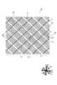
図10〜図12は、以上説明した例の変形例を示す。図10は、上部電極20の要部拡大平面図である。図11は、下部電極40の要部拡大平面図である。下部電極40が形成される透明基板には、上部電極20における断線部CL(図10)に対応する多数の補助細線25(図11)が形成されている。補助細線25は、ダミー電極35を構成する導線片と導通している。なお、図示を省略するが、上部電極20が形成される透明基板にも、下部電極40における断線部CLに対応する多数の補助細線25が形成されている。これらの補助細線25が断線部CLを埋めるため、図12に示す上部電極20と下部電極40との透視状態では、導線パターンによる格子模様が、多数の連続した細線により構成されているように見える。
前述したように、導線間のピッチに比較して断線部CLの幅は僅かな寸法であるため、補助細線25が形成されていなくても、導線パターンによる完全な格子模様が視認されるが、このように補助細線25が形成されることで、完全な格子形状がより確実に得られ、断線部CLがより視認され難くなるので好ましい。10 to 12 show modifications of the example described above. FIG. 10 is an enlarged plan view of a main part of the
As described above, since the width of the disconnection portion CL is a small dimension compared to the pitch between the conductors, even if the auxiliary
図13及び図14は、図1〜図9を参照して説明した例の他の変形例を示す。上述した断線部CLの幅は視認されにくい微小幅、例えば50μm以下に設定されるが、この場合でも、電極部分と非導電部分との光透過率の違い、反射率の違い、光沢を含む固有色の違い等により規則性のあるムラとして、断線部CLが感知されうる。本例は、この問題を解決し得る。
図13に示した上部電極20において、電極片を区画する断線部CLは、長さ方向においてその幅(断線寸法)及びその断線位置がランダムに変化するように形成されている。断線部CLの幅は、各導線の断線端部をたどる線をスムージングした線を用いて把握される。ここで、断線部CLを構成する個々の導線は、断線部CLの長手方向に沿った基準線(不図示)に対してほぼ千鳥状となる位置で、かつ断線長さを変えて断線されている。なお、導線は、規則的な千鳥状、つまり基準線の両側に交互に振れる位置で断線されていてもよいが、規則性がわかりにくいように複雑な順序で、あるいは不規則に振れる位置で断線されているほうが、断線部が視認されにくいので好ましい。また、基準線は特に設定されていなくてもよく、例えば、断線部を形成可能な領域の最大の幅寸法が設定され、この最大幅の範囲内のランダムな位置がランダムな幅で断線されていてもよい。
図示を省略するが、下部電極40においても、断線部CLの幅及び断線位置が断線部CLの長さ方向においてランダムに変化するように構成されている。13 and 14 show another modification of the example described with reference to FIGS. The width of the disconnection portion CL described above is set to a minute width that is difficult to be visually recognized, for example, 50 μm or less. However, even in this case, a difference in light transmittance between the electrode portion and the non-conductive portion, a difference in reflectance, and a characteristic including gloss The disconnection portion CL can be detected as irregularity having regularity due to a difference in color or the like. This example can solve this problem.
In the
Although not shown, the
図14は、上部電極20と下部電極40とを重ね合わせた状態の透視図である。断線部CLの幅及び断線位置がランダムとされることにより、図13に示した上部電極60単体でも、断線部CLが視認されにくいが、図14のような透視状態では、その視認されにくい効果を大きくできる。すなわち、前述の図8のように断線部CLがランダムでない直線状に形成されている場合には、透視状態で並走する上下2層の断線部CLのラインについて視認される虞がないとは言えないが、断線部CLの幅及び断線位置がランダムとされていることによって断線部CLの存在を目立ちにくくできる。 FIG. 14 is a perspective view of the state in which the
なお、図13、図14のように断線部CLの幅及び断線位置の両方がランダムでなくても、いずれか一方がランダムであることにより、断線部CLを目立たせない効果が得られるが、両方がランダムとされることにより、その効果を大きくできる。また、図13及び図14に示した断線部CLの幅及び断線位置は一例に過ぎず、断線部CLのランダムな構成は、断線部CLが規則性のあるムラとして視認されないように、断線部CLの近接する部分同士が同じランダムさとならないように決められるのが好ましい。例えば、透視状態で隣り合う電極片同士の断線長さ及び断線位置のランダムさが同一とならないように決められるのが好ましい。
更に、上部電極20と下部電極40とを重ねた際に規則性が発生しないように、上部電極側の断線部CLにおける断線長さ及び断線位置と、下部電極側の断線部CLにおける断線長さ及び断線位置とが決められるのが好ましい。In addition, even if both the width and the disconnection position of the disconnection portion CL are not random as in FIGS. 13 and 14, an effect that does not make the disconnection portion CL inconspicuous can be obtained by either one being random, By making both of them random, the effect can be increased. Moreover, the width | variety and disconnection position of the disconnection part CL shown in FIG.13 and FIG.14 are only an example, and the random structure of the disconnection part CL is a disconnection part so that the disconnection part CL is not visually recognized as regular irregularity. It is preferable that the adjacent portions of CL are determined so as not to have the same randomness. For example, it is preferable that the disconnection length and the random position of the adjacent electrode pieces in the fluoroscopic state are determined so as not to be the same.
Furthermore, in order not to generate regularity when the
次に、図15〜図22を参照して、本発明の実施形態を説明するためのタッチパネルの他の例について説明する。本例では、前述した例とは異なる導線パターンを提示する。
図15は、電極が形成されていない状態の上部電極120の部分拡大平面図である。上部電極120が形成される透明基板には、紙面の縦方向である第一方向D13と、この第一方向D13に直交し、紙面の横方向である第二方向D23とのうち第二方向D23に沿って平行に延びる複数の導線220(横線)と、これらの導線220に直交して第一方向D13に沿って延びる複数の導線210(縦線)とが形成されている。導線の数や、導線の交差角度、導線同士の間隔などが前述した上部電極20とは異なるが、本例においても、前述した例とほぼ同様に、複数の導線220を含む第二方向平行帯22が第一方向間隙S1を挟んで繰り返し形成されている。また、導線210を含む第一方向交差帯121も、前述した第一方向交差帯21とほぼ同様に形成されている。但し、本例の第一方向交差帯121は、2本の導線210を含んで形成されている。Next, another example of the touch panel for describing the embodiment of the present invention will be described with reference to FIGS. In this example, a conductor pattern different from the example described above is presented.
FIG. 15 is a partially enlarged plan view of the
ここで、第二方向平行帯22の構成については、等間隔に形成された多数の導線220から、所々で導線220を間引いた構成であることを既に述べたが、第一方向交差帯121についてもこれと同様に、等間隔に形成された多数の導線210から、所々で導線210を間引いた構成であると言える。隣り合う第一方向交差帯121と第一方向交差帯121との間では、6本の導線210が欠落している(間引かれている)。この導線210の欠落部分は、導線220で構成された第二方向平行帯22でいうところの、間隙(第一方向間隙S1)に相当する。このことは、図1〜図9を参照して説明した前述例の導線210に関しても適用可能であり、前述例(図2参照)における隣り合う第一方向交差帯21と第一方向交差帯21との間にも、1本以上の導線210が間引かれて形成された間隙が存在すると見ることができる。すなわち、多数の導線から間引くことは導線210,220に共通する構成である。 Here, the configuration of the second direction
図16は、電極列が形成されていない状態の下部電極140の部分拡大平面図である。電極列が形成されていない状態では、下部電極140の導線パターンと、図15の上部電極120の導線パターンとは同一であるが、上部電極120及び下部電極140が重ねられる際のそれぞれの向きが90度相違するため、図16は図15に対して90度回転させた状態に示される。
このため、上部電極120には第二方向D23に延びる第二方向平行帯22が形成されるのに対して、下部電極140には第一方向D13に延びる第一方向平行帯41が形成されている。また、上部電極120には第一方向D13に延びる第一方向交差帯121が形成されるのに対して、下部電極140には第二方向D23に延びる第二方向交差帯142が形成されている。FIG. 16 is a partially enlarged plan view of the
Therefore, while the second direction
図17は、第一電極列130が形成された状態の上部電極120の部分拡大平面図である。図18は、断線部CLを太い実線で示した上部電極120の平面図である。
第一電極列130は、第一方向D13に配列された四角形の複数の電極片131を有する。各電極片131は、上部電極120上に想定した菱形F3の辺(端縁線)に交差する各導線パターン210,220の一部が選択的に断線されることによって形成されている。具体的に、菱形F3の辺と導線220との交点が断線され、菱形F3の辺と導線210との交点は断線されない。つまり、電極片131の区画に際して断線されない導線210から構成される非断線部NCは、2本の導線210により形成されている。菱形F3における一方の対角の頂点はそれぞれ、第一方向交差帯121上において隣り合う二箇所の第一方向間隙S1の位置を通る。複数の導線220が断線されることにより、菱形F3の内部に電極片131が区画されるとともに、各電極片131が非断線の2本の導線210によって導通した第一電極列130が形成される。第一電極列130は、第一方向交差帯121毎に形成され、第二方向D23に繰り返し配置される。
なお、隣り合う第一電極列130,130の間には、他の導線とは導通しておらず電気的に孤立したダミー電極135が形成されている。FIG. 17 is a partially enlarged plan view of the
The
In addition, between the adjacent
図19は、第二電極列150が形成された状態の下部電極140の部分拡大平面図である。図20は、断線部CLを太い破線で示した下部電極140の平面図である。
第二電極列150は、第二方向D23に配列された四角形の複数の電極片151を有する。各電極片151は、配列方向以外は上述の電極片131と同様に形成される。すなわち、菱形F3の辺に交差する導線410,420のうち導線410は断線され、導線420は断線されない。これにより、各電極片151が2本の導線420によって導通した第二電極列150が形成される。FIG. 19 is a partially enlarged plan view of the
図21は、図17の上部電極120と図19の下部電極140とが重ねられた状態の透視平面図である。上部電極120と下部電極140とは、第一電極列130における電極片131の配列方向(第一方向D13)と、第二電極列150における電極片151の配列方向(第二方向D23)とが略直交するように、誘電層13(図1)を介して重ねられる。このように上部電極120と下部電極140とが重ねられると、上部電極120の第一方向間隙S1の位置に下部電極140の第二方向交差帯142(図19)が配置され、下部電極140の第二方向間隙S2の位置に上部電極120の第一方向交差帯121(図17)が配置される。そして、第一電極列130と第二電極列150とは互いに重ならず、これら電極列130,150がそれぞれ有する電極片31及び電極片51は、互いに重ならない状態でぎっしりと第一方向D13及び第二方向D23に配列される。第一方向間隙S1と第二方向間隙S2との交点近傍には、4つの電極片131,131,151,151がそれぞれの角を突き合わせるようにして配置されている。
本例においても、導線210,220,410,及び420の互いの交点以外には線の重なりが生じていない完全な格子模様が形成される。FIG. 21 is a perspective plan view of the state in which the
Also in this example, a complete lattice pattern in which no line overlap occurs other than the intersection of the conducting
図22は、上記の上部電極120及び下部電極140を備えるタッチパネル100及びディスプレイ9の概略構成を示す平面図である。ディスプレイ9の画像表示部91のX方向に対して、導線210,410の延出方向と同じ第一方向D13は平行であり、導線220,420の延出方向と同じ第二方向D23は直交する。また、画像表示部91のY方向に対して、導線210,410の延出方向と同じ第一方向D13は平行であり、導線220,420の延出方向と同じ第二方向D23は直交する。この構成から、タッチパネル100座標の座標軸と、ディスプレイ1座標のXY座標軸とが一致するので、座標補正処理を必要とすることなく、タッチ点の位置算出を容易に行える。この構成においては、細線のピッチをディスプレイ9の遮光部であるブラックマトリックスの整数倍にし、細線をブラックマトリックスに重ねるようにすることが好ましい。これにより、モアレの発生を防ぐことができるとともに、タッチパネル100及びディスプレイ9を透視した際の光透過率の低下(ディスプレイ画面の明るさの低下)も防ぐことができる。なお、モアレの強度を弱くするため、各導線の線幅を十分に小さくすることが好ましい。FIG. 22 is a plan view illustrating a schematic configuration of the
次に、図23〜図30を参照して、本発明の実施形態を説明するためのタッチパネルの他の例について説明する。本例では、前述した例とは異なる導線パターンを提示する。
図23は、電極が形成されていない状態の上部電極60の部分拡大平面図である。上部電極60が形成される透明基板には、前述の上部電極20(図2)とほぼ同様に、第一方向D12と、これに交差する第二方向D22とのうち第二方向D22に沿って平行に延びる複数の導線220と、これらの導線220に交差して第一方向D12に沿って延びる複数の導線210とが形成されている。導線の数や、導線の交差角度、導線同士の間隔などが前述した上部電極20とは異なるが、本例においても、複数の導線220を含む第二方向平行帯22と、導線210により構成される第一方向交差帯21とが前述の例とほぼ同様に形成されている。Next, another example of the touch panel for describing the embodiment of the present invention will be described with reference to FIGS. In this example, a conductor pattern different from the example described above is presented.
FIG. 23 is a partially enlarged plan view of the
図24は、電極列が形成されていない状態の下部電極80の部分拡大平面図である。下部電極80が形成される透明基板には、図23の上部電極60の導線パターンとは鏡像の関係となる導線パターンが形成される。上部電極60の導線パターンと下部電極80の導線パターンとは、図23、図24の上下方向を綴じ方向としたときに互いに鏡像の関係にある。すなわち、紙面の上下方向に延びる中心線を設定したときに、その中心線に関して線対称に形成されている。
上部電極60と下部電極80とは、導線パターンを相互に90度付近の角度で回転させた状態で重ねられるので、上部電極60には第二方向D22に延びる複数の導線220を含む第二方向平行帯22が形成されるのに対して、下部電極80には第一方向D12に延びる複数の導線410を含む第一方向平行帯41が形成されている。また、上部電極60には第一方向D12に延びる導線210が形成されるのに対して、下部電極80には第二方向D22に延びる導線420が形成されている。FIG. 24 is a partially enlarged plan view of the
The
図25は、第一電極列70が形成された状態の上部電極60の部分拡大平面図である。図26は、断線部CLを太い実線で示した上部電極60の平面図である。
第一電極列70は、第一方向D12と第二方向D2との両方に交差する方向に配列された四角形の複数の電極片71を有する。各電極片71は、上部電極60上に想定した四角形F2の辺(端縁線)に交差する各導線パターン210,220の一部が選択的に断線されることによって形成されている。
四角形F2は、上部電極60が形成される基板上の点Ps1と、この一点Ps1から第一方向D12及び第二方向D22の両方に交差する第三方向D3に離間する基板上の他の点Ps2とを通る。この四角形F2の辺と導線210との交差点が断線されるとともに、点Ps1及び点Ps2のそれぞれの近傍部分(非断線部NC)を除いて、四角形F2の辺と導線220との交差点も断線される。これにより、四角形F2の内部に電極片71が区画されるとともに、各電極片71が非断線部NCによって導通した第一電極列70が形成される。非断線部NCは、導線220の一部を含んで構成されている。FIG. 25 is a partially enlarged plan view of the
The
Square F2 is a point Ps1 on the substrate that the
隣り合う電極片71同士は、第三方向D3と直交する第四方向D4における位置が寸法P3だけ相違する。その結果、電極片71の配列方向は、第三方向D3と、第四方向D4の寸法P3とが合成された第五方向D5となる。
なお、隣り合う第一電極列70,70の間には、他の導線とは導通しておらず電気的に孤立したダミー電極65が形成されている。
In addition, between the adjacent
図27は、第二電極列90が形成された状態の下部電極80の部分拡大平面図である。図28は、断線部CLを太い破線で示した下部電極80の平面図である。
第二電極列90は、第一方向D12、第二方向D22、第三方向D3、及び第四方向D4のいずれにも交差する方向に配列された四角形の複数の第二電極片91を有する。各第二電極片91は、配列方向以外は上述の電極片71と同様に形成される。すなわち、四角形F2は、基板上の点Ps1と、この一点Ps1から第一方向D12、第二方向D22、及び第三方向D3のいずれにも交差する第四方向D4に離間する基板上の他の点Ps2とを通る。四角形F2の辺と導線420との交差点が断線されるとともに、点Ps1及び点Ps2のそれぞれの近傍部分である非断線部NCを除いて、四角形F2の辺と導線410との交差点も断線される。隣り合う電極片91同士は、第三方向D3における位置が寸法P3だけ相違する。その結果、電極片91の配列方向は、第四方向D4と、第三方向D3の寸法P3とが合成された第六方向D6となる。FIG. 27 is a partially enlarged plan view of the
The
図29は、図25の上部電極60と図27の下部電極80とが重ねられた状態の透視平面図である。断線部CLを太線で示している。上部電極60と下部電極80とは、第一電極列70における電極片71の配列方向(第五方向D5)と、第二電極列90における電極片91の配列方向(第六方向D6)とが直交するように、誘電層13(図1)を介して重ねられる。このように上部電極60と下部電極80とが重ねられると、上部電極60の第一方向間隙S1の位置に下部電極80の導線420(図14)が配置され、下部電極40の第二方向間隙S2の位置に上部電極60の導線210(図13)が配置される。そして、第一電極列70と第二電極列90とは互いに重ならず、第一電極列30の電極片31及び第二電極列50の電極片51は、互いに重ならない状態でぎっしりと第一方向D12及び第二方向D22に配列される。上部電極60における非断線部NCと、下部電極80における非断線部NCとの交点近傍には、4つの電極片71,71,91,91がそれぞれの角を突き合わせるようにして配置されている。
本例においても、導線210,220,410,及び420の互いの交点以外には線の重なりが生じていない完全な格子模様が形成される。FIG. 29 is a perspective plan view of the state in which the
Also in this example, a complete lattice pattern in which no line overlap occurs other than the intersection of the conducting
図30は、上記の第一、第二電極60,80を備えるタッチパネル101及びディスプレイ9の概略構成を示す平面図である。画像表示部91のX方向に対して、第五方向D5は平行であり、第六方向D6は直交する。また、画像表示部91のY方向に対して、第五方向D5は平行であり、第六方向D6は直交する。この構成から、タッチパネル101の座標の座標軸と、ディスプレイ9の座標のXY座標軸とが一致するので、座標補正処理が必要となることなく、タッチ点の位置算出を容易に行える。
このとき、各導線の延出方向である第一方向D1及び第二方向D2は、画素電極の配列方向であるX方向及びY方向の両方に対して傾斜した角度を成す。これにより、タッチパネル1の金属細線と画素電極の構造の外形や内部構造などの形状をなす辺(エッジ)とが平行関係となったり平行に近い角度に近接することが回避されるので、干渉縞の発生を抑制できる。FIG. 30 is a plan view illustrating a schematic configuration of the
At this time, the first direction D1 and the second direction D2, which are the extending directions of the conductive wires, form an angle with respect to both the X direction and the Y direction, which are the arrangement directions of the pixel electrodes. As a result, it is avoided that the metal thin line of the
図31〜図34を参照して、本発明の実施形態を説明するための抵抗膜方式タッチパネルの例について説明する。
図31は、本発明の抵抗膜方式タッチパネルの一例の断面図を模式的に示す。タッチパネル102は、指先やペンなどによってタッチされる側に配置される第一電極としての上部電極320と、この上部電極320に重ねられて、画像表示装置としてのディスプレイ9(図9)側に配置される第二電極としての下部電極340とを備える。絶縁性の透明基板12に形成された下部電極340と、可撓性の絶縁性透明フィルム16に形成された上部電極320とは、下部電極340上に形成された平面視ドット状に点在する絶縁性のスペーサ17を介在させた状態で、それぞれの四辺に沿って設けられた接着層ADによって、貼り合わせられる。An example of a resistive film type touch panel for describing an embodiment of the present invention will be described with reference to FIGS.
FIG. 31 schematically shows a cross-sectional view of an example of the resistive film type touch panel of the present invention. The
図32は、上部電極320の模式平面図である。上部電極320が形成される透明フィルム16には、紙面の横方向である第二方向D23に沿って平行に延びる複数の導線220(横線)と、これらの導線220に直交して第一方向D13に沿って延びる複数の導線210(縦線)とが形成されている。ここで、図32〜図34では、理解の容易さのために導線の数を実際よりも少なく図示している。実際の導線数は、タッチパネルの実用的な位置検出精度が得られる本数に決められる。本例においても、前述した例とほぼ同様に、複数の導線220を含む第二方向平行帯22が第一方向間隙S1を挟んで繰り返し形成されている。また、導線210を含む第一方向交差帯21も、前述した第一方向交差帯21と同様に形成されている。FIG. 32 is a schematic plan view of the
上部電極320が形成される透明フィルムの第一方向D13両端部には、一対の上部電極バスバー191,191が第一方向D23にそれぞれ沿って延出するように形成されている。第一方向交差帯21の導線210は、その両端でこれら上部電極バスバー191,191に接合され、導通している。バスバー191,191は、図示しない直流電源に接続され、バスバー191,191間には、例えば数Vの電圧が印加されるようになっている。
なお、バスバー191,191としては、金、銀、銅、ニッケルなどの金属あるいはカーボンなどの導電性を有するペーストを用いることができる。バスバー191,191の形成方法としては、スクリーン印刷、オフセット印刷、グラビア印刷、フレキソ印刷などの印刷法、フォトレジスト法、刷毛塗法などがある。The first direction D13 at both ends of the transparent film
The bus bars 191 and 191 can be made of a metal such as gold, silver, copper, or nickel, or a conductive paste such as carbon. Examples of methods for forming the bus bars 191 and 191 include screen printing, offset printing, gravure printing, flexographic printing, and other printing methods, a photoresist method, and a brush coating method.
本例の導線パターンには、上述の各例のように断線部が形成されておらず、本例の導線パターンは複数の電極片、あるいはこれを連ねた電極列には区画されていない。すなわち、互いに格子状に交差する導線210,220は互いに導通して一つの電極を形成する。 The conductor pattern of this example is not formed with a disconnection portion as in each of the above-described examples, and the conductor pattern of this example is not partitioned into a plurality of electrode pieces or an electrode array in which these are connected. That is, the conducting
図33は、下部電極340の模式平面図である。下部電極340の導線パターンは、図32の上部電極320の導線パターンと同一であり、図33は図32に対して90度回転させた状態に示されている。
このため、下部電極340には第一方向D13に延びる第一方向平行帯41と、第二方向D23に延びる第二方向交差帯42とがそれぞれ形成されている。FIG. 33 is a schematic plan view of the
Therefore, the first direction
下部電極340が形成される透明基板の第二方向D23両端部には、一対の下部電極バスバー192,192が第一方向D13にそれぞれ沿って延出するように形成されている。第二方向交差帯42の導線420は、その両端でこれら下部電極バスバー192,192に接合され、導通している。これら下部電極バスバー192,192は、上部電極バスバー191,191と同様に形成され、図示しない直流電源によって例えば数Vの電圧が印加される。The second direction D23 at both ends of the transparent substrate where the
また、図33には図示を省略したが、下部電極340には、多数の絶縁性のスペーサー17(図31)がドット状に点在するように形成される。これらのスペーサー17は、上部電極320に向かって突出しており、これによって上部電極320と下部電極340とが接触せずに、上部電極320と下部電極340との間に空間が形成される。なお、スペーサー17は、上部電極320に形成されていてもよい。
スペーサー17は、メラミンアクリレート樹脂、ウレタンアクリレート樹脂、エポキシアクリレート樹脂、メタアクリルアクリレート樹脂、アクリルアクリレート樹脂などのアクリレート樹脂、ポリビニールアルコール樹脂などの透明な光硬化型樹脂をフォトプロセスで微細なドット状に形成して得ることができる。また、印刷法により微細なドットを多数形成してスペーサーとすることもできる。Although not shown in FIG. 33, the
The
図34は、図32の上部電極320と図33の下部電極340とが重ねられた状態の透視平面図である。なお、本図において、スペーサー17及び接着層ADの図示は省略している。このように上部電極320と下部電極340とが重ねられると、上部電極320の第一方向間隙S1の位置に下部電極340の第二方向交差帯42(図33)が配置され、下部電極340の第二方向間隙S2の位置に上部電極320の第一方向交差帯21(図32)が配置される。これにより、導線210,220,410,及び420の互いの交点以外には線の重なりが生じていない完全な格子模様が形成される。 34 is a perspective plan view of the state in which the
このような構成のタッチパネル102では、指やペンなどにより、上部電極320の裏面(上部電極320が形成される透明フィルム12のタッチ側の面)をタッチすると、スペーサー17がない位置(タッチ位置)で上部電極320と下部電極340とが接触して導通する。この際、上部電極320のバスバー191,191間への電圧印加時における第一方向D13の電圧勾配に基づいてタッチ位置のX座標が測定されるとともに、下部電極340のバスバー192,192間への電圧印加時における第二方向D23の電圧勾配とに基づいてタッチ位置のY座標が測定される。具体的に、X座標測定時には下部電極340には電圧印加されず、タッチ位置での接触導通による上部電極バスバー191,191間の印加電圧の分圧が下部電極340のバスバー192,192間の電位として出力される。また、Y座標測定時には上部電極320には電圧印加されず、タッチ位置での接触導通による下部電極バスバー192,192間の印加電圧の分圧が上部電極320のバスバー191,191間の電位として出力される。これら分圧とバスバー間の距離、及びバスバー間の印加電圧とから、タッチ位置のXY座標がそれぞれ測定される。
本例においても、図15〜図22を参照して説明した例と同様に、タッチパネルの座標とディスプレイの座標とが一致するので、座標変換を不要にできる。In the
Also in this example, as in the example described with reference to FIGS. 15 to 22, the coordinates of the touch panel and the coordinates of the display coincide with each other, so that coordinate conversion can be made unnecessary.
なお、上部電極320の導線パターン形成領域に形成されたすべての導線210の合計の電気抵抗、及び下部電極340の導線パターン形成領域に形成されたすべての導線420の合計の電気抵抗はそれぞれ、100Ωから5kΩの範囲にあることが好ましく、200Ωから2kΩであることが特に好ましい。
また、上部電極バスバー191,191、及び下部電極バスバー192,192のそれぞれは、導線パターン形成領域であるタッチセンサー領域の外側にあって、図示しないディスプレイ窓枠部などによって操作者からは視認されない位置に隠されている。このため、バスバー191,192の線幅は導線よりも十分に大きくできるので、タッチ位置検出時のバスバーによる電位降下は無視できる。The total electrical resistance of all the
Each of the upper
本例では、4線式の抵抗膜方式によるタッチパネル102を示したが、この他、5線式、6線式、7線式、8線式などの抵抗膜方式にも本発明は適用可能である。 In this example, the
以上で説明した上部電極及び下部電極のそれぞれの導線パターンを形成することのできる導電性材料と電極形成方法について以下の[1]で説明する。
[1] 上部電極及び下部電極はそれぞれ、導電性細線による電極であり、低抵抗である導電性の高い金属又は合金を用いることが好ましい。このような金属としては、例えば、銅、銀、金、白金、パラジウム、ニッケル、錫、アルミニウム、コバルト、ロジウム、イリジウム、鉄、ルテニウム、オスミウム、マンガン、モリブデン、タングステン、ニオブ、タンテル、チタン、ビスマス、アンチモン、鉛などをあげることができる。これらの中で導電性に優れる点で、銅、銀、金、白金、パラジウム、ニッケル、錫、アルミニウム、及びこれらとの合金が好ましい。ここで、上部電極及び下部電極には、特に比抵抗が類似の材料が用いられることが好ましい。上部電極及び下部電極は、基本的には同じ導電材料により形成されるが、異なる導電性材料により形成されていてもよい。In the following [1], the conductive material and the electrode forming method capable of forming the conductor patterns of the upper electrode and the lower electrode described above will be described.
[1] Each of the upper electrode and the lower electrode is an electrode made of a conductive thin wire, and it is preferable to use a metal or alloy having high resistance and low resistance. Examples of such metals include copper, silver, gold, platinum, palladium, nickel, tin, aluminum, cobalt, rhodium, iridium, iron, ruthenium, osmium, manganese, molybdenum, tungsten, niobium, tantel, titanium, and bismuth. , Antimony, lead and the like. Among these, copper, silver, gold, platinum, palladium, nickel, tin, aluminum, and alloys thereof are preferable in terms of excellent conductivity. Here, it is preferable that a material having a specific resistance is particularly used for the upper electrode and the lower electrode. The upper electrode and the lower electrode are basically formed of the same conductive material, but may be formed of different conductive materials.
これらの金属あるいは合金での電極形成には、以下の形態[2]〜[4]の利用ができる。
[2] 金属箔、あるいは薄膜としての利用。薄膜として利用するには、まず、基材上に上記の金属あるいは合金を、真空蒸着法、スパッターリング法、イオンプレーティング法などによって、あるいは鍍金法や金属箔の貼り合わせなどで金属薄膜を形成する。次いでこの金属薄膜に以下のパターニングを施して電極を形成する。上記パターンをフォトエッチングにより形成する場合、金属薄膜上にフォトレジスト膜を形成しフォトマスクを用いて露光し、現像液で現像することによりレジスト膜のパターンを形成する。これをエッチング液によりエッチングし、レジスト膜を剥離除去することにより細線金属線からなるパターンを形成する。あるいは、印刷レジストにより形成する場合は、金属薄膜上にスクリーン印刷、グラビア印刷、インクジェット等の方法でレジスト膜のパターンを印刷し、エッチング液により金属薄膜におけるレジスト被覆部以外をエッチングし、レジスト膜を剥離することにより金属細線のパターンを形成する。The following modes [2] to [4] can be used for forming electrodes with these metals or alloys.
[2] Use as metal foil or thin film. To use as a thin film, first form a metal thin film on the base material by vacuum deposition, sputtering, ion plating, or by plating or bonding metal foil. To do. Next, the metal thin film is subjected to the following patterning to form an electrode. When the pattern is formed by photoetching, a photoresist film is formed on the metal thin film, exposed using a photomask, and developed with a developer to form a resist film pattern. This is etched with an etching solution, and the resist film is peeled and removed to form a pattern made of fine metal wires. Alternatively, in the case of forming with a printing resist, a resist film pattern is printed on the metal thin film by a method such as screen printing, gravure printing, or ink jet, and the resist film is etched except for the resist coating portion in the metal thin film with an etching solution. A pattern of fine metal wires is formed by peeling.
[3] 導電性のナノ粒子を含むインク(又はペースト)によって上記のパターンを印刷する方法である。導電性ナノ粒子は、上記の金属の微粒子の他にカーボンを用いてもよい。導電性ナノ粒子は金、銀、パラジウム、白金、銅、カーボン、又はそれらの混合物を含む粒子が好ましい。ナノ粒子の平均粒径は2μ以下、好ましくは200から500nmであり、従来のミクロン粒子よりも粒径が小さいものがパターンを形成する上で好ましい。パターン印刷には、スクリーン印刷法又はグラビア印刷法が用いられる。
インク(又はペースト)が含む導電材料は、金属粒子でなく、導電性繊維であってもよい。本件においては、導電性繊維には、金属ワイヤー、ナノワイヤーと呼ばれる繊維状の物質、中空構造のチューブ、ナノチューブを含めて呼称する。金属ナノワイヤーの平均短軸長さ(「平均短軸径」、「平均直径」と称することがある)としては、100nm以下が好ましく、1nm〜50nmがより好ましく、10nm〜40nmが更に好ましく、15nm〜35nmが特に好ましい。導電性繊維を用いて導電層を形成する場合には、例えば、特開2009-215594、特開2009-242880、特開2009-299162、特開2010-84173、特開2010-87105、特開2010-86714に開示の技術を組み合わせて形成することができる。[3] A method of printing the above pattern with an ink (or paste) containing conductive nanoparticles. In addition to the above metal fine particles, carbon may be used as the conductive nanoparticles. The conductive nanoparticles are preferably particles containing gold, silver, palladium, platinum, copper, carbon, or a mixture thereof. The average particle size of the nanoparticles is 2 μm or less, preferably 200 to 500 nm, and those having a particle size smaller than that of conventional micron particles are preferable for forming a pattern. A screen printing method or a gravure printing method is used for pattern printing.
The conductive material included in the ink (or paste) may be conductive fibers instead of metal particles. In the present case, the conductive fiber includes a metal wire, a fibrous substance called nanowire, a hollow structure tube, and a nanotube. The average minor axis length of the metal nanowire (sometimes referred to as “average minor axis diameter” or “average diameter”) is preferably 100 nm or less, more preferably 1 nm to 50 nm, still more preferably 10 nm to 40 nm, and even more preferably 15 nm. -35 nm is particularly preferred. In the case of forming a conductive layer using conductive fibers, for example, JP2009-215594, JP2009-242880, JP2009-299162, JP2010-84173, JP2010-87105, JP2010. -86714 can be combined with the disclosed technology.
[4] 写真に用いられるハロゲン化銀写真感光材料を用い、この材料にパターン露光を施した後に現像、定着処理をし、現像銀による導電性の細線パターンを得る方法である。本発明における導電性の細線パターンを得る方法には、感光材料と現像処理の形態によって、次の3通りの形態が含まれる。
(a) 物理現像核を含まない感光性ハロゲン化銀黒白感光材料を化学現像又は熱現像して金属銀部を該感光材料上に形成させる態様。
(b) 物理現像核をハロゲン化銀乳剤層中に含む感光性ハロゲン化銀黒白感光材料を溶解物理現像して金属銀部を該感光材料上に形成させる態様。
(c) 物理現像核を含まない感光性ハロゲン化銀黒白感光材料と、物理現像核を含む非感光性層を有する受像シートを重ね合わせて拡散転写現像して金属銀部を非感光性受像シート上に形成させる態様。[4] In this method, a silver halide photographic light-sensitive material used for photography is used, and this material is subjected to pattern exposure and then developed and fixed to obtain a conductive fine line pattern by developed silver. The method for obtaining a conductive fine line pattern in the present invention includes the following three forms depending on the photosensitive material and the form of development processing.
(a) An embodiment in which a photosensitive silver halide black-and-white photosensitive material not containing physical development nuclei is chemically or thermally developed to form a metallic silver portion on the photosensitive material.
(b) An embodiment in which a photosensitive silver halide black-and-white photosensitive material containing physical development nuclei in a silver halide emulsion layer is dissolved and physically developed to form a metallic silver portion on the photosensitive material.
(c) A photosensitive silver halide black-and-white photosensitive material that does not contain physical development nuclei and an image-receiving sheet having a non-photosensitive layer that contains physical development nuclei are overlaid and diffusion transferred to develop a metallic silver portion on the non-photosensitive image-receiving sheet. Form formed on top.
上記(a)の態様は、一体型黒白現像タイプであり、感光材料上に光透過性導電膜等の透光性導電性膜が形成される。得られる現像銀は化学現像銀又は熱現像銀であり、高比表面のフィラメントである点で後続するめっき又は物理現像過程で活性が高い。
上記(b)の態様は、露光部では、物理現像核近縁のハロゲン化銀粒子が溶解されて現像核上に沈積することによって感光材料上に光透過性導電性膜等の透光性導電性膜が形成される。これも一体型黒白現像タイプである。現像作用が、物理現像核上への析出であるので高活性であるが、現像銀は比表面の小さい球形である。
上記(c)の態様は、未露光部においてハロゲン化銀粒子が溶解されて拡散して受像シート上の現像核上に沈積することによって受像シート上に光透過性導電性膜等の透光性導電性膜が形成される。いわゆるセパレートタイプであって、受像シートを感光材料から剥離して用いる態様である。The mode (a) is an integrated black-and-white development type, and a light-transmitting conductive film such as a light-transmitting conductive film is formed on the photosensitive material. The resulting developed silver is chemically developed silver or heat developed silver, and is highly active in the subsequent plating or physical development process in that it is a filament with a high specific surface.
In the aspect (b), the light-transmitting conductive film such as a light-transmitting conductive film is formed on the photosensitive material by dissolving silver halide grains close to the physical development nucleus and depositing on the development nucleus in the exposed portion. A characteristic film is formed. This is also an integrated black-and-white development type. Although the development action is precipitation on the physical development nuclei, it is highly active, but developed silver is a sphere with a small specific surface.
In the embodiment (c), the silver halide grains are dissolved and diffused in the unexposed area and deposited on the development nuclei on the image receiving sheet, thereby translucent such as a light transmissive conductive film on the image receiving sheet. A conductive film is formed. This is a so-called separate type in which the image receiving sheet is peeled off from the photosensitive material.
いずれの態様もネガ型現像処理及び反転現像処理のいずれの現像を選択することもできる(拡散転写方式の場合は、感光材料としてオートポジ型感光材料を用いることによってネガ型現像処理が可能となる)。 In either embodiment, either negative development processing or reversal development processing can be selected (in the case of the diffusion transfer method, negative development processing is possible by using an auto-positive type photosensitive material as the photosensitive material). .
ここでいう化学現像、熱現像、溶解物理現像、拡散転写現像は、当業界で通常用いられている用語どおりの意味であり、写真化学の一般教科書、例えば菊地真一著「写真化学」(共立出版社、1955年刊行)、C.E.K.Mees編「The Theory of Photographic Processes, 4th ed.」(Mcmillan社、1977年刊行)に解説されている。本件は液処理に係る発明であるが、その他の現像方式として熱現像方式を適用する技術も参考にすることができる。例えば、特開2004−184693号、同2004−334077号、同2005−010752号の各公報、特願2004−244080号、同2004−085655号の各明細書に記載された技術を適用することができる。
また、本発明に用いる材料と導電性パターンの製法については、電磁波シールド膜の発明である特開2006−352073号の記載と技術、静電容量方式のタッチパネルの発明である特願2009−265467号の記載と技術を用いることができる。The chemical development, thermal development, dissolution physical development, and diffusion transfer development mentioned here have the same meanings as are commonly used in the industry, and are general textbooks of photographic chemistry such as Shinichi Kikuchi, “Photochemistry” (Kyoritsu Publishing) (Published in 1955), C.I. E. K. It is described in "The Theory of Photographic Processes, 4th ed." Edited by Mees (Mcmillan, 1977). Although this case is an invention related to liquid processing, a technique of applying a thermal development system as another development system can also be referred to. For example, the techniques described in Japanese Patent Application Laid-Open Nos. 2004-184893, 2004-334077, and 2005-010752, and Japanese Patent Application Nos. 2004-244080 and 2004-085655 can be applied. it can.
In addition, regarding the material used in the present invention and the method for producing a conductive pattern, the description and technology of JP-A-2006-352073 which is an invention of an electromagnetic shielding film, and Japanese Patent Application No. 2009-265467 which is an invention of a capacitive touch panel. Can be used.
なお、上部電極及び下部電極にそれぞれ使用される導電性材料が光透過性を有している必要はないが、光透過性のある導電性材料もまた、上部電極及び下部電極のそれぞれに使用可能である。光透過性のある導電性材料としては、導電性ポリマーや一部の金属酸化物を挙げることができるが耐久性、耐候性の点で金属酸化物が用いられる。透明金属酸化物としては、インジウムスズ酸化物(ITO)、アンチモンドープスズ酸化物(ATO)、酸化スズ、アルミニウムドープの亜鉛酸化物(ZnO:Al)、インジウム亜鉛酸化物(In2O3−ZnO(IZO))などをあげることができる。本発明では、下部電極を形成する電極片として上記の透明酸化物を用いることができ、上記の酸化物のうち、抵抗値、透明性、膜の形成のしやすさの観点から、ITOやIZOが好ましく用いられる。ITOやIZOの薄膜の形成には、スパッタ法、電子ビーム法やイオンプレーティング法などが用いられる。
上部電極及び下部電極には、上記[1]以下に例示したすべての材料を使用できる。Note that the conductive material used for each of the upper electrode and the lower electrode does not have to be light transmissive, but a light transmissive conductive material can also be used for each of the upper electrode and the lower electrode. It is. Examples of the light-transmitting conductive material include conductive polymers and some metal oxides, but metal oxides are used in terms of durability and weather resistance. Transparent metal oxides include indium tin oxide (ITO), antimony-doped tin oxide (ATO), tin oxide, aluminum-doped zinc oxide (ZnO: Al), and indium zinc oxide (In2O3-ZnO (IZO)). ) Etc. In the present invention, the above transparent oxide can be used as an electrode piece for forming the lower electrode. Among the above oxides, from the viewpoint of resistance value, transparency, and ease of film formation, ITO and IZO Is preferably used. A sputtering method, an electron beam method, an ion plating method, or the like is used to form a thin film of ITO or IZO.
For the upper electrode and the lower electrode, all materials exemplified in the above [1] and below can be used.
ここで、電極形成材料として、金属箔、あるいは薄膜としての利用(上記[2])の場合の形成方法を図35を参照しながら説明する。図35は、上部電極(図4、図17、図25等)の形成方法を示すが、下部電極も上部電極と同様に形成される。
図35の(a)は絶縁層を兼ねる透明基体160(図1の透明基板11又は透明基板12に相当)であり、たとえば約100μmのPETフィルムである。このフィルムの表面を清浄化し、次いでこのフィルムの表面に、金属あるいは合金の薄層200を設ける(図35の(b))。金属は上記[2]に記載した材料を用いることができるが、銀、銅、アルミニウムあるいはこれらの合金が好ましく用いられる。薄層の形成方法にはスパッタ法などが用いられるが、他の方法であってもよい。形成した金属の薄層の厚みは、所望の抵抗値により適宜調整することができるが、0.1μm以上3μm以下が好ましく、0.2μm以上1μm以下がより好ましい。
次に上記で形成した金属薄膜200上にフォトレジスト膜を形成しフォトマスクを用いて露光し、現像液で現像することによりレジスト膜のパターンを形成する。これをエッチング液によりエッチングし、レジスト膜を剥離除去することにより金属細線からなる導線パターン201を形成する(図35の(c))。このようなフォトリソグラフィー及びエッチングによるパターニング工程により、図4、図17、図25にそれぞれ示したような、断線部CLを有する上部電極の導線パターンが形成される。下部電極の導線パターンも、上部電極の導線パターンと同様に形成される。Here, a forming method in the case of use as a metal foil or a thin film as the electrode forming material (the above [2]) will be described with reference to FIG. FIG. 35 shows a method of forming the upper electrode (FIGS. 4, 17, 25, etc.), but the lower electrode is formed in the same manner as the upper electrode.
FIG. 35 (a) shows a
Next, a photoresist film is formed on the metal
次に、上記で形成された導線パターンに設けられる被覆層の形成について述べる。なお、この被覆層は形成されていなくてもよい。この被覆層を黒化層と呼ぶ。黒化層は、金属あるいは合金の金属光沢を目立たなくする視覚的機能と、金属の防錆、マイグレーション防止による耐久性向上の機能を持つ。この黒化層(被覆層)の材料については以下で別途説明する。黒化層(被覆層)の厚みは、5μm以下が好ましく、3μm以下がより好ましく、0.2μm以上2μm以下が特に好ましい。
図35の(d)のように、導線パターン201及び透明基体160表面の全体を被覆する黒化層170を形成した後、この黒化層170の電極細線を被覆していないパターン形成領域上の黒化層部分を除去し、導線パターン201のみを被覆する黒化層171を形成する(図35の(e))。これにより、視認性、耐久性に優れた導線パターン電極を形成することができるNext, formation of the coating layer provided on the conductive wire pattern formed above will be described. In addition, this coating layer does not need to be formed. This coating layer is called a blackening layer. The blackened layer has a visual function that makes the metallic luster of the metal or alloy inconspicuous, and a function of improving durability by preventing rust and migration of the metal. The material for the blackening layer (coating layer) will be described separately below. The thickness of the blackening layer (coating layer) is preferably 5 μm or less, more preferably 3 μm or less, and particularly preferably 0.2 μm or more and 2 μm or less.
As shown in FIG. 35D, after forming the blackened
次に上記の黒化層(被覆層)の形成材料と形成方法について説明する。黒色層の好適な積層方法の例としては、メッキ処理とケミカルエッチング法を挙げることができる。
メッキ処理としては公知の黒色メッキと呼ばれるものであれば何でも使用して良く、黒色niメッキ、黒色Crメッキ、黒色Sn−ni合金メッキ、Sn−ni−Cu合金メッキ、黒色亜鉛クロメート処理等が例として挙げられる。具体的には、日本化学産業(株)製の黒色メッキ浴(商品名、ニッカブラック、Sn−ni合金系)、(株)金属化学工業製の黒色メッキ浴(商品名、エボニ−クロム85シリ−ズ、Cr系)、ディップソール(株)性クロメート剤(商品名、ZB−541、亜鉛メッキ黒色クロメート剤)を使用することができる。メッキ法としては無電解メッキ、電解メッキのどちらの方法でも良く、緩やかな条件であっても高速メッキであっても良い。メッキ厚みは黒色として認知できれば厚みは限定されないが、通常のメッキ厚みは1μm〜5μmが好適である。Next, the forming material and forming method of the blackening layer (coating layer) will be described. Examples of suitable lamination methods for the black layer include plating and chemical etching.
Any known so-called black plating may be used as the plating treatment, such as black ni plating, black Cr plating, black Sn-ni alloy plating, Sn-ni-Cu alloy plating, black zinc chromate treatment, etc. As mentioned. Specifically, black plating bath (trade name, Nikka Black, Sn-ni alloy system) manufactured by Nippon Chemical Industry Co., Ltd., black plating bath (trade name, Ebony-Chromium 85 series manufactured by Metal Chemical Industry Co., Ltd.) -Cr, Cr) and dip sole Co., Ltd. chromate agent (trade name, ZB-541, galvanized black chromate agent) can be used. The plating method may be either electroless plating or electrolytic plating, and may be mild or high-speed plating. Although the thickness is not limited as long as the plating thickness can be recognized as black, the normal plating thickness is preferably 1 μm to 5 μm.
導電性金属部の一部を酸化処理若しくは硫化処理して黒色部を形成することもできる。例えば導電性金属部が銅である場合、銅表面の黒化処理剤の例としては、メルテックス(株)製、商品名エンプレートMB438A,B、三菱瓦斯化学(株)製、商品名nPE−900、メック(株)製、商品名メックエッチボンドBO−7770V、アイソレ−ト化学研究所製、商品名コパ−ブラックCuO、同CuS、セレン系のコパ− ブラックno.65等を使用することができる。上記の他には例えば、硫化物を処理して硫化水素(H 2S)を発生させ、銅の表面を硫化銅(CuS)として黒化することももちろん可能である。これらの処理は黒色として認知できれば厚みは限定されないが、通常3μm以下が好ましく、0.2μm〜2μmが更に好ましい。 A black part can also be formed by oxidizing or sulfurating a part of the conductive metal part. For example, when the conductive metal part is copper, examples of the blackening treatment agent on the copper surface include: Meltex Co., Ltd., trade name Enplate MB438A, B, Mitsubishi Gas Chemical Co., Ltd., trade name: nPE- 900, manufactured by Mec Co., Ltd., trade name Mec Etch Bond BO-7770V, manufactured by Isolate Chemical Laboratories, trade name Copa-Black CuO, CuS, selenium-based Copa Black no. 65 etc. can be used. In addition to the above, for example, it is possible to treat the sulfide to generate hydrogen sulfide (H 2 S) and to blacken the copper surface as copper sulfide (CuS). The thickness of the treatment is not limited as long as it can be recognized as black, but it is preferably 3 μm or less, more preferably 0.2 μm to 2 μm.
導電性のナノ粒子を含むインク(又はペースト)を用いる場合(上[3])には、絶縁層を兼ねる透明基体層に、上記のパターンを直接印刷することができる。 When an ink (or paste) containing conductive nanoparticles is used (upper [3]), the above pattern can be directly printed on the transparent substrate layer also serving as an insulating layer.
次に、電極形成材料として、写真に用いられるハロゲン化銀写真感光材料を用いる場合(上記の[4])について図36を用いて説明する。図36は、上部電極(図4、図17、図25等)の形成方法を示すが、下部電極も上部電極と同様に形成される。
なお、本発明に用いるハロゲン化銀写真感光材料については、現像銀による細線パターンを用いた電磁波シールド膜の発明である特開2006−352073号に詳細に説明されている。
図36(a)は絶縁層を兼ねる透明基体160であり、たとえば約100μmのPETフィルムである。このフィルムの表面を清浄化し、次いでこのフィルムの表面に、ハロゲン化銀写真感光材料の薄層250を設ける(図36の(b))。ハロゲン化銀写真感光材料には、光センサーとしての特性に優れるハロゲン化銀、ゼラチンなどのバインダー、塗布助剤や感度調整用の各種添加剤が含まれる。塗布銀量(銀塩の塗布量)は、銀に換算して1〜30g/m2が好ましく、1〜25g/m2がより好ましく、5〜20g/m2が更に好ましい。塗布銀量を上記範囲とすることで、露光、現像処理後の導電シートが所望の表面抵抗を得ることができる。薄膜の形成は、写真材料の製造に用いられる多層塗布機を用いることが好ましい。Next, the case of using a silver halide photographic light-sensitive material used for photography ([4] above) will be described with reference to FIG. FIG. 36 shows a method of forming the upper electrode (FIGS. 4, 17, 25, etc.), but the lower electrode is formed in the same manner as the upper electrode.
The silver halide photographic light-sensitive material used in the present invention is described in detail in JP-A No. 2006-352073, which is an invention of an electromagnetic wave shielding film using a fine line pattern of developed silver.
FIG. 36A shows a
次に上記のハロゲン化銀写真感光材料の薄層250に導電性の細線を形成するためにパターン状の露光を施す。図36(c)では露光により感光核が生成された領域を251で示した。この露光済みのフィルムに現像定着処理を施した後のフィルムを図36(d)で表した。252は現像により感光核周辺に形成された銀の集合体を表し、253は感光しなかったハロゲン化銀写真感光材料部分に含まれる銀塩などが定着処理により層外に除かれ透明な膜となった状態を表している。このようにして現像銀による細線パターンを形成することができる。 Next, in order to form conductive thin lines on the
以上説明したように、本明細書には、
第一方向と、前記第一方向に交差する第二方向とのうち第二方向に沿って互いに平行に延びる複数の導線が配置された第二方向平行帯が前記第一方向の第一方向間隙を挟んで前記第一方向に繰り返し形成され、かつ前記第一方向に沿って延びて前記第二方向平行帯に交差する導線が配置された第一方向交差帯が前記第二方向に繰り返し形成された第一電極と、
前記第一方向に沿って互いに平行に延びる複数の導線が配置された第一方向平行帯が前記第二方向の第二方向間隙を挟んで前記第二方向に繰り返し形成され、かつ前記第二方向に沿って延びて前記第一方向平行帯に交差する導線が配置された第二方向交差帯が前記第一方向に繰り返し形成された第二電極と、を備え、
前記第一方向間隙の位置に前記第二方向交差帯が対応し、前記第二方向間隙の位置に前記第一方向交差帯が対応するように、前記第一電極と前記第二電極とが互いに重ねられることを特徴とするタッチパネルが開示されている。As described above, the present specification includes
The first direction gap in the first direction is a second direction parallel band in which a plurality of conductive wires extending in parallel with each other along the second direction are arranged among the first direction and the second direction intersecting the first direction. A first direction crossing band is repeatedly formed in the second direction. The first direction crossing band is disposed in the first direction with the conductors extending along the first direction and intersecting the second direction parallel band. The first electrode,
A first-direction parallel strip in which a plurality of conductive wires extending in parallel with each other along the first direction is repeatedly formed in the second direction across the second-direction gap in the second direction, and the second direction A second electrode in which a second direction crossing band in which a conductive wire extending along the first direction parallel band is arranged is repeatedly formed in the first direction, and
The first electrode and the second electrode are mutually connected so that the second direction crossing band corresponds to the position of the first direction gap and the first direction crossing band corresponds to the position of the second direction gap. A touch panel characterized by being overlaid is disclosed.
このタッチパネルによれば、第一電極と第二電極とを重ね合わせる際の誤差や、導線の形状誤差に対する許容度が大きく、重ね合わせが少々ずれていたり導線の形状にバラツキがあったとしても線太りや干渉縞が生じにくいので、導線の格子形状に違和感を感じない新規な導線パターンを歩留まり良く、安価に得られる。また、導線の間隔(ピッチ)を狭くしても線太りや干渉縞が生じにくいことから、導線の配置密度を高くして接触の検知感度を向上させることが可能となる。
なお、導線パターンとして低抵抗の金属細線を採用し得ることで良好な応答性が得られるため、大画面や高精細のディスプレイに対応するタッチパネルを提供できる。According to this touch panel, even if there is a large tolerance for errors in overlaying the first electrode and the second electrode and the shape error of the conductor, even if the overlay is slightly shifted or the conductor shape varies, Since thickening and interference fringes are less likely to occur, a new conductor pattern that does not give a sense of incongruity to the grid shape of the conductor can be obtained with good yield and at low cost. Further, even if the interval (pitch) between the conductive wires is narrowed, line thickening and interference fringes are less likely to occur. Therefore, it is possible to increase the arrangement density of the conductive wires and improve the contact detection sensitivity.
In addition, since a favorable responsiveness is acquired by being able to employ | adopt a low resistance metal fine wire as a conducting wire pattern, the touch panel corresponding to a large screen or a high-definition display can be provided.
また、本明細書に開示されたタッチパネルにおいては、
前記第一電極及び前記第二電極を透視したとき、
前記第一方向平行帯及び前記第一方向交差帯のそれぞれに含まれる各導線は、互いに一定間隔で並び、
前記第二方向平行帯及び前記第二方向交差帯のそれぞれに含まれる各導線は、互いに一定間隔で並び、
前記第一方向平行帯、前記第二方向平行帯、前記第一方向交差帯、及び前記第二方向交差帯により、均一な格子模様が形成される。In the touch panel disclosed in this specification,
When seeing through the first electrode and the second electrode,
The conducting wires included in each of the first direction parallel band and the first direction crossing band are arranged at regular intervals from each other,
The conducting wires included in each of the second direction parallel band and the second direction crossing band are arranged at regular intervals from each other,
A uniform lattice pattern is formed by the first direction parallel band, the second direction parallel band, the first direction cross band, and the second direction cross band.
このタッチパネルによれば、導線パターンが形成される透明基体上の面内導線分布が均一化されるので、導線パターンを極力視認されないようにできる。 According to this touch panel, since the in-plane conductor distribution on the transparent substrate on which the conductor pattern is formed is made uniform, the conductor pattern can be prevented from being seen as much as possible.
また、本明細書に開示されたタッチパネルにおいては、
前記第一方向平行帯を構成する導線及び前記第二方向平行帯を構成する導線のそれぞれの数は3本以上であり、
前記第一方向交差帯を構成する導線及び前記第二方向交差帯を構成する導線のそれぞれの数は1本以上10本以下であって、前記第一方向平行帯を構成する導線及び前記第二方向平行帯を構成する導線のそれぞれの数よりも少ない。In the touch panel disclosed in this specification,
The number of each of the conducting wires constituting the first direction parallel strip and the conducting wires constituting the second direction parallel strip is three or more,
The number of each of the conducting wires constituting the first direction crossing band and the conducting wires constituting the second direction crossing band is 1 or more and 10 or less, and the conducting wires constituting the first direction parallel band and the second Less than the number of each of the conducting wires constituting the directional parallel strip.
このタッチパネルによれば、導線の上記本数から、第1、第2電極の重ね合わせによる格子模様を形成し易い。また、第1、第2電極のそれぞれの導線パターンを複数の電極に断線区画する場合には、導線の上記本数から、複数の平行導線がこれら平行導線を横断する導線により導通された一纏まりの領域を形成し易いので、電極を形成し易い。 According to this touch panel, it is easy to form a lattice pattern by superimposing the first and second electrodes based on the number of the conductive wires. In addition, when the conductor pattern of each of the first and second electrodes is divided into a plurality of electrodes, a group of a plurality of parallel conductors connected by conductors crossing these parallel conductors is determined from the above number of conductors. Since it is easy to form a region, it is easy to form an electrode.
また、本明細書に開示されたタッチパネルにおいては、
前記第一方向平行帯及び前記第二方向平行帯のそれぞれに含まれる複数の前記導線は、前記第一方向交差帯及び前記第二方向交差帯のそれぞれのピッチよりも小さいピッチで密に配置される。
このタッチパネルによれば、密に配置された導線群をそれよりも疎に配置された導線により互いに導通することにより、第1、第2電極の重ねあわせによる格子模様を形成し易いとともに、電極を区画形成する場合に一纏まりの領域としての電極片を形成し易い。ここで、密な配置の導線群が小さいピッチで配置されていることで、接触検知の感度を高くできるとともに、電極片同士を導通する導線の配置が疎であることにより、第一電極列と第二電極列とを透視状態で重ならないように配列するパターン設計が煩雑化しない。In the touch panel disclosed in this specification,
The plurality of conductive wires included in each of the first direction parallel band and the second direction parallel band are densely arranged at a pitch smaller than the pitch of each of the first direction cross band and the second direction cross band. The
According to this touch panel, it is easy to form a lattice pattern by superimposing the first and second electrodes by conducting a densely arranged conductor group with a conductor arranged more sparsely, and the electrodes In the case of partition formation, it is easy to form electrode pieces as a group of regions. Here, since the densely arranged conductor groups are arranged at a small pitch, the sensitivity of contact detection can be increased, and the arrangement of the conductors that conduct the electrode pieces to each other is sparse, so that the first electrode array and The pattern design for arranging the second electrode rows so as not to overlap in the fluoroscopic state does not become complicated.
また、本明細書に開示されたタッチパネルにおいては、
前記第一方向平行帯及び前記第二方向平行帯のそれぞれに含まれる複数の前記導線のピッチは、150μm以上、400μm以下であり、
前記第一方向交差帯及び前記第二方向交差帯のそれぞれのピッチは、2000μm以上、10000μm以下である。In the touch panel disclosed in this specification,
The pitch of the plurality of conducting wires included in each of the first direction parallel strip and the second direction parallel strip is 150 μm or more and 400 μm or less,
Each pitch of the first direction crossing band and the second direction crossing band is 2000 μm or more and 10,000 μm or less.
このタッチパネルによれば、上記ピッチから、第1、第2電極の重ね合わせによる格子模様を形成し易い。また、第1、第2電極のそれぞれの導線パターンを複数の電極に断線区画する場合には、電極を形成し易い。 According to this touch panel, it is easy to form a lattice pattern by overlapping the first and second electrodes from the pitch. Moreover, when each conducting wire pattern of the first and second electrodes is divided into a plurality of electrodes, the electrodes are easily formed.
また、本明細書に開示されたタッチパネルにおいては、
前記第一電極の前記第一方向交差帯は、前記第二電極にそれぞれ形成された前記第一方向平行帯及び前記第二方向間隙の合計の幅と等しいピッチで配列され、
前記第二電極の前記第二方向交差帯は、前記第一電極にそれぞれ形成された前記第二方向平行帯及び前記第一方向間隙の合計の幅と等しいピッチで配列される。In the touch panel disclosed in this specification,
The first direction crossing band of the first electrode is arranged at a pitch equal to the total width of the first direction parallel band and the second direction gap respectively formed on the second electrode,
The second direction crossing bands of the second electrode are arranged at a pitch equal to the total width of the second direction parallel band and the first direction gap respectively formed on the first electrode.
このタッチパネルによれば、線太りや干渉縞を防止でき、導線の格子形状に違和感を感じない新規な導線パターンを歩留まり良く、安価に得られる。 According to this touch panel, it is possible to prevent line thickening and interference fringes, and to obtain a new conductive wire pattern that does not give a sense of incongruity to the lattice shape of the conductive wire with a good yield and low cost.
また、本明細書に開示されたタッチパネルにおいては、
前記第一方向平行帯及び前記第二方向平行帯をそれぞれ構成する導線の幅は、2μm以上、10μm以下であり、
前記第一方向平行帯及び前記第二方向平行帯のそれぞれにおける前記導線のピッチは、250μm以上、350μm以下である。In the touch panel disclosed in this specification,
The widths of the conductive wires constituting the first direction parallel strip and the second direction parallel strip are 2 μm or more and 10 μm or less,
The pitch of the conducting wire in each of the first direction parallel strip and the second direction parallel strip is 250 μm or more and 350 μm or less.
このタッチパネルによれば、上記の線幅及びピッチより、視認性(導線やモアレが視認され難い)と感度との両方がバランス良く得られる。 According to this touch panel, both visibility (conducting wire and moire is difficult to be visually recognized) and sensitivity can be obtained in a balanced manner from the above line width and pitch.
また、本明細書に開示されたタッチパネルにおいては、
前記第一電極は、当該第一電極上に想定した閉図形の端縁線に交差する前記各導線の部分が選択的に断線されることによって区画された電極片が配列された第一電極列を有し、
前記第二電極は、当該第二電極上に想定した閉図形の端縁線に交差する前記各導線の一部が選択的に断線されることによって区画された電極片が前記第一電極列の配列方向と交差する方向に配列された第二電極列を有し、
前記第一電極列及び前記第二電極列は、互いに交差するそれぞれの一定方向に繰り返し配置され、
前記第一電極と前記第二電極とを透視したときに、前記各電極片が互いに重ならない状態に配列される。In the touch panel disclosed in this specification,
The first electrode is a first electrode array in which electrode pieces partitioned by selectively disconnecting portions of the conductive wires that intersect the edge line of the closed figure assumed on the first electrode are arranged. Have
In the second electrode, an electrode piece partitioned by selectively disconnecting a part of each conductive wire that intersects an edge line of a closed figure assumed on the second electrode is the first electrode row. Having a second electrode array arranged in a direction crossing the arrangement direction;
The first electrode row and the second electrode row are repeatedly arranged in a certain direction intersecting each other,
When the first electrode and the second electrode are seen through, the electrode pieces are arranged so as not to overlap each other.
このタッチパネルによれば、第一、第二電極のそれぞれの導線パターンを適切な位置で断線することにより、第一電極列及び第二電極列がそれぞれ形成され、第一、第二電極を重ねた際に交差する第一、第二電極列によってタッチ位置座標が形成される。第一、第二電極が重ねられた際の透視状態において電極片同士が重ならずにぎっしりと並ぶので、接触検知の感度を高感度にできる。また、電極片の形成と同時にダミー電極も形成されるため、大画面や高精細なディスプレイに対応するタッチパネルの高周波駆動時の短絡を防止できる。 According to this touch panel, the first electrode row and the second electrode row are formed by disconnecting the respective conductive wire patterns of the first and second electrodes at appropriate positions, and the first and second electrodes are overlapped. Touch position coordinates are formed by the first and second electrode rows that intersect each other. In the fluoroscopic state when the first and second electrodes are overlaid, the electrode pieces are closely arranged without overlapping each other, so that the sensitivity of contact detection can be increased. In addition, since the dummy electrode is formed simultaneously with the formation of the electrode piece, it is possible to prevent a short circuit during high frequency driving of a touch panel corresponding to a large screen or a high definition display.
また、本明細書に開示されたタッチパネルにおいては、
前記第一電極に含まれる複数の前記導線のパターンと、前記第二電極に含まれる複数の前記導線のパターンとは、互いに鏡像の関係にある。
このタッチパネルによれば、鏡像であることで、導線のパターン設計のコストを削減できる。In the touch panel disclosed in this specification,
The plurality of conductive wire patterns included in the first electrode and the plurality of conductive wire patterns included in the second electrode are in a mirror image relationship with each other.
According to this touch panel, since it is a mirror image, it is possible to reduce the cost of pattern design of the conductive wire.
また、本明細書に開示されたタッチパネルにおいては、
前記第一電極列の前記各電極片は、前記第一方向交差帯上の二箇所の前記第一方向間隙の位置を通る閉図形の端縁線に交差する前記第二方向平行帯の部分が断線されることによって前記閉図形の内部に形成されるとともに、前記第一方向交差帯の導線により互いに導通された状態で前記第一方向に配列され、
前記第二電極列の前記各電極片は、前記第二方向交差帯上の二箇所の前記第二方向間隙の位置を通る閉図形の端縁線に交差する前記第一方向平行帯の部分が断線されることによって前記閉図形の内部に形成されるとともに、前記第二方向交差帯の導線により互いに導通された状態で前記第二方向に配列される。
このタッチパネルによれば、第一、第二電極を重ねた際に、格子模様に違和感を感じない新規な電極列配置パターンが得られる。In the touch panel disclosed in this specification,
Each electrode piece of the first electrode row has a portion of the second direction parallel band that intersects an edge line of a closed figure passing through the positions of the two first direction gaps on the first direction cross band. It is formed inside the closed figure by being disconnected, and is arranged in the first direction in a state of being electrically connected to each other by the conducting wires of the first direction crossing band,
Each of the electrode pieces of the second electrode array has a portion of the first direction parallel band that intersects an edge line of a closed figure passing through the positions of the two second direction gaps on the second direction cross band. By being disconnected, it is formed inside the closed figure, and is arranged in the second direction in a state of being electrically connected to each other by the conducting wires in the second direction crossing band.
According to this touch panel, when the first and second electrodes are overlapped, a novel electrode array arrangement pattern that does not give a sense of incongruity to the lattice pattern is obtained.
また、本明細書に開示されたタッチパネルにおいては、
前記第一電極列の前記各電極片は、前記第一電極上の一点とこの一点から前記第一方向及び前記第二方向の両方に交差する第三方向に離間する前記第一電極上の他の点とを通る閉図形の端縁線に交差する前記第一方向交差帯の部分、及び前記閉図形の端縁線に交差する前記第二方向平行帯における前記一点及び前記他の点のそれぞれの近傍の非断線部を除いた部分が断線されることによって前記閉図形の内部に形成されるとともに、前記非断線部を介して互いに導通された状態で配列され、
前記第二電極列の前記各電極片は、前記第二電極上の一点とこの一点から前記第一方向、前記第二方向、及び前記第三方向のいずれにも交差する第四方向に離間する前記第二電極上の他の点とを通る閉図形の端縁線に交差する前記第二方向交差帯の部分、及び前記閉図形の端縁線に交差する前記第一方向平行帯における前記一点及び前記他の点のそれぞれの近傍の非断線部を除いた部分が断線されることによって前記閉図形の内部に形成されるとともに、前記非断線部を介して互いに導通された状態で配列される。
このタッチパネルによれば、第一、第二電極を重ねた際に、格子模様に違和感を感じない新規な電極列配置パターンが得られる。In the touch panel disclosed in this specification,
Each of the electrode pieces of the first electrode array includes a point on the first electrode and another on the first electrode spaced from the one point in a third direction intersecting both the first direction and the second direction. A portion of the first direction crossing band that intersects the edge line of the closed graphic passing through the point, and the one point and the other point in the second direction parallel band that intersects the edge line of the closed graphic Is formed inside the closed figure by disconnecting the part other than the non-disconnected portion in the vicinity of, and arranged in a state of being electrically connected to each other through the non-disconnected portion,
Each electrode piece of the second electrode row is separated from a point on the second electrode and a fourth direction intersecting any of the first direction, the second direction, and the third direction from the one point. The portion of the second direction crossing band that intersects the edge line of the closed graphic passing through another point on the second electrode, and the one point in the first direction parallel band that intersects the edge line of the closed graphic And the portions other than the non-disconnected portion in the vicinity of each of the other points are formed inside the closed figure by being disconnected, and are arranged in a state of being electrically connected to each other through the non-disconnected portion. .
According to this touch panel, when the first and second electrodes are overlapped, a novel electrode array arrangement pattern that does not give a sense of incongruity to the lattice pattern is obtained.
また、本明細書に開示されたタッチパネルにおいては、
前記第一方向に沿って延びる導線及び前記第二方向に沿って延びる導線はそれぞれ、当該タッチパネルに積層されるディスプレイが有する画素の配列方向に対して傾斜する。
このタッチパネルによれば、導線パターンを構成する各導線と画素のエッジ等との光干渉が生じ難いので、干渉縞(モアレ)の発生を防止できる。In the touch panel disclosed in this specification,
The conducting wires extending along the first direction and the conducting wires extending along the second direction are inclined with respect to the arrangement direction of the pixels included in the display stacked on the touch panel.
According to this touch panel, it is difficult for optical interference between each conductor constituting the conductor pattern and the edge of the pixel or the like to occur, so that occurrence of interference fringes (moire) can be prevented.
また、本明細書に開示されたタッチパネルにおいては、
当該タッチパネルに積層される画像表示装置が有する画素の配列方向に対して、前記第一方向は平行又は直交に、前記第二方向は直交又は平行に、それぞれ設定される。
このタッチパネルによれば、タッチ点の位置座標と画像表示装置のXY座標とが、座標補正などを行うことなく一致するので、タッチ位置の算出処理を容易に行うことができる。In the touch panel disclosed in this specification,
The first direction is set in parallel or perpendicular to the pixel arrangement direction of the image display device stacked on the touch panel, and the second direction is set orthogonal or parallel.
According to this touch panel, since the position coordinates of the touch point and the XY coordinates of the image display device match without performing coordinate correction or the like, the touch position calculation process can be easily performed.
また、本明細書に開示されたタッチパネルにおいては、
前記閉図形の端縁線に交差し断線された前記各導線の部分の集合である断線部において前記端縁線に交差する方向の断線寸法、及び前記端縁線に交差する方向の断線位置の少なくとも一方は、前記端縁線に沿った方向においてランダムに変化する。
このタッチパネルによれば、断線部が直線状に形成される場合と比較して、導線パターンが規則性のあるムラとして視認され難くなる。すなわち、タッチパネルの搭載によるディスプレイの表示品位の低下を防止できる。In the touch panel disclosed in this specification,
The disconnection size in the direction intersecting the edge line in the disconnection part, which is a set of portions of the respective conductors that intersect and disconnect the edge line of the closed figure, and the disconnection position in the direction intersecting the edge line At least one changes randomly in the direction along the edge line.
According to this touch panel, the conductive wire pattern is less likely to be visually recognized as regular irregularity as compared with the case where the disconnection portion is formed in a straight line. That is, it is possible to prevent the display quality of the display from being lowered due to the mounting of the touch panel.
また、本明細書に開示されたタッチパネルにおいては、
前記電極片の区画に際して断線されない導線の部分を含んで構成される非断線部は、2本以上の導線により形成される。
このタッチパネルによれば、電極列を構成する各電極片が複数本の導線により導通されるので、複数の導線のうち一部の導線が使用時の焼損などによって断線しても、導通を確保できる。In the touch panel disclosed in this specification,
The non-breaking portion including the portion of the conducting wire that is not broken when the electrode pieces are partitioned is formed by two or more conducting wires.
According to this touch panel, each electrode piece constituting the electrode row is electrically connected by a plurality of conductors, so that even if some of the plurality of conductors are disconnected due to burnout during use or the like, conduction can be ensured. .
また、本明細書に開示されたタッチパネルにおいては、
前記閉図形は、多角形である。
このタッチパネルによれば、電極片が多角形とされることで、第一、第二方向にそれぞれ延びる導線群から電極片を形成し易い。In the touch panel disclosed in this specification,
The closed figure is a polygon.
According to this touch panel, since the electrode pieces are polygonal, the electrode pieces can be easily formed from the conductive wire groups extending in the first and second directions.
また、本明細書には、
上記のタッチパネルと、
前記タッチパネルが積層されるディスプレイとを備える画像表示装置が開示されている。
この画像表示装置によれば、前述の構成のタッチパネルを備えることにより、前述と同様の作用及び効果を享受できる。In addition, in this specification,
The above touch panel;
An image display device including a display on which the touch panel is stacked is disclosed.
According to this image display device, by providing the touch panel having the above-described configuration, the same operations and effects as described above can be enjoyed.
なお、本発明は、下記表1及び表2に記載の公開公報及び国際公開パンフレットの技術と適宜組合わせて使用することができる。「特開」、「号公報」、「号パンフレット」等の表記は省略する。 In addition, this invention can be used in combination with the technique of the publication gazette and international publication pamphlet which are described in following Table 1 and Table 2. FIG. Notations such as “JP,” “Gazette” and “No. Pamphlet” are omitted.

AD 接着層
CL 断線部
D1 第一方向
D12 第一方向
D13 第一方向
D2 第二方向
D22 第二方向
D23 第二方向
D3 第三方向
D4 第四方向
D5 第五方向
D6 第六方向
F1 四角形
F2 四角形
F3 菱形
NC 非断線部
P1 ピッチ
P2 ピッチ
Ps1 点
Ps2 点
S1 第一方向間隙
S2 第二方向間隙
1〜3 タッチパネル
9 ディスプレイ
9A 画像表示部
9B 額縁部
11 透明基板
12 透明基板
13 誘電層
13 誘電層
14 粘着層
15 透明カバー部材
16 透明フィルム
17 ドットスペーサー
18 導線パターン形成領域
20 上部電極(第一電極)
21 第一方向交差帯
22 第二方向平行帯
25 補助細線
30 下部電極(第二電極)
30 第一電極列
31 電極片
35 ダミー電極
40 下部電極(第二電極)
41 第一方向平行帯
42 第二方向交差帯
50 第二電極列
51 電極片
60 上部電極(第一電極)
65 ダミー電極
70 第一電極列
71 電極片
80 下部電極(第二電極)
90 第二電極列
91 電極片
210 導線
220 導線
410 導線
420 導線
100 タッチパネル
101 タッチパネル
102 タッチパネル
120 上部電極(第一電極)
121 第一方向交差帯
130 第一電極列
135 ダミー電極
131 電極片
140 下部電極(第二電極)
142 第二方向交差帯
150 第二電極列
151 電極片
191 上部電極バスバー
192 下部電極バスバー
320 上部電極(第一電極)
340 下部電極(第二電極)AD adhesive layer CL Disconnected portion D1 First direction D12 First direction D13 First direction D2 Second direction D22 Second direction D23 Second direction D3 Third direction D4 Fourth direction D5 Fifth direction D6 Sixth direction F1 Square F2 Square F3 Rhombus NC Non-breaking part P1 Pitch P2 Pitch Ps1 Point Ps2 Point S1 First direction gap S2 Second direction gap 1-3
21 First
30
41 First direction
65
90
121 First
142 Second
340 Lower electrode (second electrode)
Claims (17)
Translated fromJapanese前記第一方向に沿って互いに平行に延びる複数の導線が配置された第一方向平行帯が前記第二方向の第二方向間隙を挟んで前記第二方向に繰り返し形成され、かつ前記第二方向に沿って延びて前記第一方向平行帯に交差する導線が配置された第二方向交差帯が前記第一方向に繰り返し形成された第二電極と、を備え、
前記第一電極において前記第一方向間隙には導線が配置されておらず、かつ前記第二電極において前記第二方向間隙には導線が配置されておらず、
前記第一方向間隙の位置に前記第二方向交差帯が対応し、前記第二方向間隙の位置に前記第一方向交差帯が対応するように、前記第一電極と前記第二電極とが互いに重ねられることを特徴とするタッチパネル。The first direction gap in the first direction is a second direction parallel band in which a plurality of conductive wires extending in parallel with each other along the second direction are arranged among the first direction and the second direction intersecting the first direction. A first direction crossing band is repeatedly formed in the second direction. The first direction crossing band is disposed in the first direction with the conductors extending along the first direction and intersecting the second direction parallel band. The first electrode,
A first-direction parallel strip in which a plurality of conductive wires extending in parallel with each other along the first direction is repeatedly formed in the second direction across the second-direction gap in the second direction, and the second direction A second electrode in which a second direction crossing band in which a conductive wire extending along the first direction parallel band is arranged is repeatedly formed in the first direction, and
No conducting wire is arranged in the first direction gap in the first electrode, and no conducting wire is arranged in the second direction gap in the second electrode,
The first electrode and the second electrode are mutually connected so that the second direction crossing band corresponds to the position of the first direction gap and the first direction crossing band corresponds to the position of the second direction gap. A touch panel characterized by being overlaid.
前記第一電極及び前記第二電極を透視したとき、
前記第一方向平行帯及び前記第一方向交差帯のそれぞれに含まれる各導線は、互いに一定間隔で並び、
前記第二方向平行帯及び前記第二方向交差帯のそれぞれに含まれる各導線は、互いに一定間隔で並び、
前記第一方向平行帯、前記第二方向平行帯、前記第一方向交差帯、及び前記第二方向交差帯により、均一な格子模様が形成されることを特徴とするタッチパネル。The touch panel according to claim 1,
When seeing through the first electrode and the second electrode,
The conducting wires included in each of the first direction parallel band and the first direction crossing band are arranged at regular intervals from each other,
The conducting wires included in each of the second direction parallel band and the second direction crossing band are arranged at regular intervals from each other,
The touch panel, wherein a uniform lattice pattern is formed by the first direction parallel band, the second direction parallel band, the first direction cross band, and the second direction cross band.
前記第一方向平行帯を構成する導線及び前記第二方向平行帯を構成する導線のそれぞれの数は3本以上であり、
前記第一方向交差帯を構成する導線及び前記第二方向交差帯を構成する導線のそれぞれの数は1本以上10本以下であって、前記第一方向平行帯を構成する導線及び前記第二方向平行帯を構成する導線のそれぞれの数よりも少ないことを特徴とするタッチパネル。The touch panel according to claim 1 or 2,
The number of each of the conducting wires constituting the first direction parallel strip and the conducting wires constituting the second direction parallel strip is three or more,
The number of each of the conducting wires constituting the first direction crossing band and the conducting wires constituting the second direction crossing band is 1 or more and 10 or less, and the conducting wires constituting the first direction parallel band and the second A touch panel characterized in that the number is smaller than the number of conductors constituting the directional parallel strip.
前記第一方向平行帯及び前記第二方向平行帯のそれぞれに含まれる複数の前記導線は、前記第一方向交差帯及び前記第二方向交差帯のそれぞれのピッチよりも小さいピッチで密に配置されることを特徴とするタッチパネル。The touch panel according to any one of claims 1 to 3,
The plurality of conductive wires included in each of the first direction parallel band and the second direction parallel band are densely arranged at a pitch smaller than the pitch of each of the first direction cross band and the second direction cross band. A touch panel characterized by that.
前記第一方向平行帯及び前記第二方向平行帯のそれぞれに含まれる複数の前記導線のピッチは、150μm以上、400μm以下であり、
前記第一方向交差帯及び前記第二方向交差帯のそれぞれのピッチは、2000μm以上、10000μm以下であることを特徴とするタッチパネル。The touch panel according to claim 4,
The pitch of the plurality of conducting wires included in each of the first direction parallel strip and the second direction parallel strip is 150 μm or more and 400 μm or less,
Each of the pitches of the first direction crossing band and the second direction crossing band is 2000 μm or more and 10,000 μm or less.
前記第一電極の前記第一方向交差帯は、前記第二電極にそれぞれ形成された前記第一方向平行帯及び前記第二方向間隙の合計の幅と等しいピッチで配列され、
前記第二電極の前記第二方向交差帯は、前記第一電極にそれぞれ形成された前記第二方向平行帯及び前記第一方向間隙の合計の幅と等しいピッチで配列されることを特徴とするタッチパネル。The touch panel according to any one of claims 1 to 5,
The first direction crossing band of the first electrode is arranged at a pitch equal to the total width of the first direction parallel band and the second direction gap respectively formed on the second electrode,
The second direction crossing bands of the second electrode are arranged at a pitch equal to a total width of the second direction parallel band and the first direction gap formed respectively on the first electrode. Touch panel.
前記第一方向平行帯及び前記第二方向平行帯をそれぞれ構成する導線の幅は、2μm以上、10μm以下であり、
前記第一方向平行帯及び前記第二方向平行帯のそれぞれにおける前記導線のピッチは、250μm以上、350μm以下であることを特徴とするタッチパネル。The touch panel according to any one of claims 1 to 6,
The widths of the conductive wires constituting the first direction parallel strip and the second direction parallel strip are 2 μm or more and 10 μm or less,
The pitch of the said conducting wire in each of said 1st direction parallel strip and said 2nd direction parallel strip is 250 micrometers or more and 350 micrometers or less, The touch panel characterized by the above-mentioned.
前記第一電極は、当該第一電極上に想定した閉図形の端縁線に交差する前記各導線の部分が選択的に断線されることによって区画された電極片が配列された第一電極列を有し、
前記第二電極は、当該第二電極上に想定した閉図形の端縁線に交差する前記各導線の一部が選択的に断線されることによって区画された電極片が前記第一電極列の配列方向と交差する方向に配列された第二電極列を有し、
前記第一電極列及び前記第二電極列は、互いに交差するそれぞれの一定方向に繰り返し配置され、
前記第一電極と前記第二電極とを透視したときに、前記各電極片が互いに重ならない状態に配列されることを特徴とするタッチパネル。The touch panel according to any one of claims 1 to 7,
The first electrode is a first electrode array in which electrode pieces partitioned by selectively disconnecting portions of the conductive wires that intersect the edge line of the closed figure assumed on the first electrode are arranged. Have
In the second electrode, an electrode piece partitioned by selectively disconnecting a part of each conductive wire that intersects an edge line of a closed figure assumed on the second electrode is the first electrode row. Having a second electrode array arranged in a direction crossing the arrangement direction;
The first electrode row and the second electrode row are repeatedly arranged in a certain direction intersecting each other,
The touch panel, wherein the electrode pieces are arranged so as not to overlap each other when the first electrode and the second electrode are seen through.
前記第一電極に含まれる複数の前記導線のパターンと、前記第二電極に含まれる複数の前記導線のパターンとは、互いに鏡像の関係にあることを特徴とするタッチパネル。The touch panel according to claim 8,
The touch panel, wherein the plurality of conductive wire patterns included in the first electrode and the plurality of conductive wire patterns included in the second electrode are in a mirror image relationship with each other.
前記第一電極列の前記各電極片は、前記第一方向交差帯上の二箇所の前記第一方向間隙の位置を通る閉図形の端縁線に交差する前記第二方向平行帯の部分が断線されることによって前記閉図形の内部に形成されるとともに、前記第一方向交差帯の導線により互いに導通された状態で前記第一方向に配列され、
前記第二電極列の前記各電極片は、前記第二方向交差帯上の二箇所の前記第二方向間隙の位置を通る閉図形の端縁線に交差する前記第一方向平行帯の部分が断線されることによって前記閉図形の内部に形成されるとともに、前記第二方向交差帯の導線により互いに導通された状態で前記第二方向に配列されることを特徴とするタッチパネル。The touch panel according to claim 8 or 9, wherein
Each electrode piece of the first electrode row has a portion of the second direction parallel band that intersects an edge line of a closed figure passing through the positions of the two first direction gaps on the first direction cross band. It is formed inside the closed figure by being disconnected, and is arranged in the first direction in a state of being electrically connected to each other by the conducting wires of the first direction crossing band,
Each of the electrode pieces of the second electrode array has a portion of the first direction parallel band that intersects an edge line of a closed figure passing through the positions of the two second direction gaps on the second direction cross band. The touch panel is formed in the closed figure by being disconnected and arranged in the second direction in a state of being electrically connected to each other by the conductive wires in the second direction crossing band.
前記第一電極列の前記各電極片は、前記第一電極上の一点とこの一点から前記第一方向及び前記第二方向の両方に交差する第三方向に離間する前記第一電極上の他の点とを通る閉図形の端縁線に交差する前記第一方向交差帯の部分、及び前記閉図形の端縁線に交差する前記第二方向平行帯における前記一点及び前記他の点のそれぞれの近傍の非断線部を除いた部分が断線されることによって前記閉図形の内部に形成されるとともに、前記非断線部を介して互いに導通された状態で配列され、
前記第二電極列の前記各電極片は、前記第二電極上の一点とこの一点から前記第一方向、前記第二方向、及び前記第三方向のいずれにも交差する第四方向に離間する前記第二電極上の他の点とを通る閉図形の端縁線に交差する前記第二方向交差帯の部分、及び前記閉図形の端縁線に交差する前記第一方向平行帯における前記一点及び前記他の点のそれぞれの近傍の非断線部を除いた部分が断線されることによって前記閉図形の内部に形成されるとともに、前記非断線部を介して互いに導通された状態で配列されることを特徴とするタッチパネル。The touch panel according to claim 8 or 9, wherein
Each of the electrode pieces of the first electrode array includes a point on the first electrode and another on the first electrode spaced from the one point in a third direction intersecting both the first direction and the second direction. A portion of the first direction crossing band that intersects the edge line of the closed graphic passing through the point, and the one point and the other point in the second direction parallel band that intersects the edge line of the closed graphic Is formed inside the closed figure by disconnecting the part other than the non-disconnected portion in the vicinity of, and arranged in a state of being electrically connected to each other through the non-disconnected portion,
Each electrode piece of the second electrode row is separated from a point on the second electrode and a fourth direction intersecting any of the first direction, the second direction, and the third direction from the one point. The portion of the second direction crossing band that intersects the edge line of the closed graphic passing through another point on the second electrode, and the one point in the first direction parallel band that intersects the edge line of the closed graphic And the portions other than the non-disconnected portion in the vicinity of each of the other points are formed inside the closed figure by being disconnected, and are arranged in a state of being electrically connected to each other through the non-disconnected portion. A touch panel characterized by that.
前記第一方向に沿って延びる導線及び前記第二方向に沿って延びる導線はそれぞれ、当該タッチパネルに積層されるディスプレイが有する画素の配列方向に対して傾斜することを特徴とするタッチパネル。The touch panel according to any one of claims 1 to 11,
The conductive wire extending along the first direction and the conductive wire extending along the second direction are each inclined with respect to an arrangement direction of pixels of a display stacked on the touch panel.
当該タッチパネルに積層されるディスプレイが有する画素の配列方向に対して、前記第一方向は平行又は直交に、前記第二方向は直交又は平行に、それぞれ設定されることを特徴とするタッチパネル。The touch panel according to any one of claims 1 to 11,
The touch panel, wherein the first direction is set to be parallel or perpendicular to the pixel arrangement direction of the display stacked on the touch panel, and the second direction is set to be orthogonal or parallel.
前記閉図形の端縁線に交差し断線された前記各導線の部分の集合である断線部において前記端縁線に交差する方向の断線寸法、及び前記端縁線に交差する方向の断線位置の少なくとも一方は、前記端縁線に沿った方向においてランダムに変化することを特徴とするタッチパネル。The touch panel according to any one of claims 8 to 13,
The disconnection size in the direction intersecting the edge line in the disconnection part, which is a set of portions of the respective conductors that intersect and disconnect the edge line of the closed figure, and the disconnection position in the direction intersecting the edge line At least one of the touch panels changes randomly in a direction along the edge line.
前記電極片の区画に際して断線されない導線の部分を含んで構成される非断線部は、2本以上の導線により形成されることを特徴とするタッチパネル。The touch panel according to any one of claims 11 to 14,
The non-breaking part comprised including the part of the conducting wire which is not disconnected at the time of the division of the said electrode piece is formed with two or more conducting wires.
前記閉図形は、多角形であることを特徴とするタッチパネル。The touch panel according to any one of claims 8 to 15,
The touch panel, wherein the closed figure is a polygon.
前記タッチパネルが積層されるディスプレイとを備える画像表示装置。The touch panel according to any one of claims 1 to 16,
An image display device comprising: a display on which the touch panel is stacked.
Priority Applications (5)
| Application Number | Priority Date | Filing Date | Title |
|---|---|---|---|
| JP2010249208AJP5647864B2 (en) | 2010-11-05 | 2010-11-05 | Touch panel |
| CN201180064252.5ACN103282866B (en) | 2010-11-05 | 2011-10-31 | touch panel |
| PCT/JP2011/075118WO2012060344A1 (en) | 2010-11-05 | 2011-10-31 | Touch panel |
| TW100140166ATWI552036B (en) | 2010-11-05 | 2011-11-03 | Touch panel and image display device |
| US13/886,654US9295176B2 (en) | 2010-11-05 | 2013-05-03 | Touch panel |
Applications Claiming Priority (1)
| Application Number | Priority Date | Filing Date | Title |
|---|---|---|---|
| JP2010249208AJP5647864B2 (en) | 2010-11-05 | 2010-11-05 | Touch panel |
Publications (2)
| Publication Number | Publication Date |
|---|---|
| JP2012103761A JP2012103761A (en) | 2012-05-31 |
| JP5647864B2true JP5647864B2 (en) | 2015-01-07 |
Family
ID=46024458
Family Applications (1)
| Application Number | Title | Priority Date | Filing Date |
|---|---|---|---|
| JP2010249208AActiveJP5647864B2 (en) | 2010-11-05 | 2010-11-05 | Touch panel |
Country Status (5)
| Country | Link |
|---|---|
| US (1) | US9295176B2 (en) |
| JP (1) | JP5647864B2 (en) |
| CN (1) | CN103282866B (en) |
| TW (1) | TWI552036B (en) |
| WO (1) | WO2012060344A1 (en) |
Families Citing this family (105)
| Publication number | Priority date | Publication date | Assignee | Title |
|---|---|---|---|---|
| KR102381391B1 (en)* | 2015-04-16 | 2022-03-31 | 삼성디스플레이 주식회사 | Display device |
| TW201310291A (en)* | 2011-08-17 | 2013-03-01 | Wintek Corp | Touch display panel |
| US9612265B1 (en) | 2011-09-23 | 2017-04-04 | Cypress Semiconductor Corporation | Methods and apparatus to detect a conductive object |
| US8903679B2 (en) | 2011-09-23 | 2014-12-02 | Cypress Semiconductor Corporation | Accuracy in a capacitive sense array |
| US8819927B2 (en)* | 2012-02-28 | 2014-09-02 | Eastman Kodak Company | Method of making a transparent conductor structure |
| JP2013206198A (en)* | 2012-03-28 | 2013-10-07 | Nissha Printing Co Ltd | Touch sensor |
| JP6324656B2 (en)* | 2012-07-12 | 2018-05-16 | 大日本印刷株式会社 | Touch panel substrate and display device |
| WO2014021168A1 (en)* | 2012-07-31 | 2014-02-06 | シャープ株式会社 | Touch panel substrate and display device |
| US20150220176A1 (en)* | 2012-08-02 | 2015-08-06 | Sharp Kabushiki Kaisha | Touch panel substrate and display device |
| WO2014021226A1 (en)* | 2012-08-02 | 2014-02-06 | シャープ株式会社 | Touch panel substrate and display device |
| US8907920B2 (en) | 2012-08-13 | 2014-12-09 | J Touch Corporation | Complex sensing electrode structure applied to a touch panel |
| TWI478033B (en)* | 2012-09-07 | 2015-03-21 | E Ink Holdings Inc | Capacitive structure of capacitive touch panel |
| JP2014063353A (en)* | 2012-09-21 | 2014-04-10 | J Touch Corp | Compound detection electrode structure used in touch panel |
| WO2014050306A1 (en) | 2012-09-26 | 2014-04-03 | 三菱電機株式会社 | Touch screen |
| JP5987191B2 (en)* | 2012-10-17 | 2016-09-07 | 三菱電機株式会社 | Touch screen, touch panel, and display device including the same |
| JP5896886B2 (en)* | 2012-11-20 | 2016-03-30 | 三菱電機株式会社 | SUBSTRATE WITH TOUCH SCREEN FOR DISPLAY DEVICE, METHOD FOR DESIGNING SUBSTRATE WITH TOUCH SCREEN FOR DISPLAY DEVICE, AND DISPLAY DEVICE WITH TOUCH SCREEN |
| JP2014106974A (en)* | 2012-11-22 | 2014-06-09 | Lg Innotek Co Ltd | Touch window |
| US9229553B2 (en)* | 2012-11-30 | 2016-01-05 | 3M Innovative Properties Company | Mesh patterns for touch sensor electrodes |
| EP2738653B1 (en)* | 2012-12-03 | 2021-05-19 | LG Innotek Co., Ltd. | Electrode member and touch panel including the same |
| JP6031980B2 (en) | 2012-12-04 | 2016-11-24 | 三菱電機株式会社 | touch screen |
| JP6037816B2 (en)* | 2012-12-18 | 2016-12-07 | 三菱電機株式会社 | Touch panel and display device including the same |
| JP6001089B2 (en)* | 2012-12-18 | 2016-10-05 | 富士フイルム株式会社 | Display device and method for determining pattern of conductive film |
| TWI620281B (en)* | 2013-01-09 | 2018-04-01 | 寶威光電有限公司 | Sensor module package structure and method for manufacturing the same |
| JP5910761B2 (en)* | 2013-01-25 | 2016-04-27 | 凸版印刷株式会社 | Touch panel and display device |
| WO2014119230A1 (en)* | 2013-01-29 | 2014-08-07 | シャープ株式会社 | Input apparatus, manufacturing method therefor, and electronic information device |
| CN104956296A (en)* | 2013-01-29 | 2015-09-30 | 夏普株式会社 | Input device, manufacturing method thereof, and electronic information device |
| CN103970318B (en)* | 2013-01-29 | 2017-09-05 | 新加坡商宝威光电有限公司 | Sensing module packaging structure and manufacturing method thereof |
| JP2014149608A (en)* | 2013-01-31 | 2014-08-21 | Dainippon Printing Co Ltd | Flexible electrode member for touch panel, touch panel and image display device |
| CN103187118B (en)* | 2013-02-06 | 2015-02-18 | 南昌欧菲光科技有限公司 | Conductive film, manufacturing method for conductive film and touch screen with conductive film |
| US9047053B2 (en) | 2013-02-06 | 2015-06-02 | Nanchang O-Film Tech. Co., Ltd. | Conductive film, method for manufacturing the same and touch screen having the same |
| JP5870945B2 (en)* | 2013-02-28 | 2016-03-01 | 三菱電機株式会社 | Touch screen, touch panel, display device and electronic device |
| KR102057655B1 (en)* | 2013-03-07 | 2019-12-23 | 삼성디스플레이 주식회사 | Touch Screen Panel |
| TWI505335B (en) | 2013-03-18 | 2015-10-21 | Touch Crporation J | Touch sensing electrode structure |
| JP2014203421A (en)* | 2013-04-10 | 2014-10-27 | 株式会社タッチパネル研究所 | Capacitive touch panel |
| JP2014219963A (en)* | 2013-04-12 | 2014-11-20 | 信越ポリマー株式会社 | Sheet for sensor sheet production, method for producing the same, sensor sheet for touchpad, and method for producing the same |
| JP6013397B2 (en)* | 2013-05-10 | 2016-10-25 | サムソン エレクトロ−メカニックス カンパニーリミテッド. | Touch sensor |
| WO2014185115A1 (en)* | 2013-05-16 | 2014-11-20 | シャープ株式会社 | Touch panel substrate and electronic apparatus |
| TWI576729B (en)* | 2013-05-17 | 2017-04-01 | 群創光電股份有限公司 | Touch display panel and touch display apparatus |
| US20160179234A1 (en)* | 2013-07-03 | 2016-06-23 | Amosense Co., Ltd. | Touch sensor for touch screen panel, manufacturing method thereof, and touch screen panel including same |
| US9383781B2 (en)* | 2013-08-06 | 2016-07-05 | Samsung Electro-Mechanics Co., Ltd. | Touch sensor |
| JP2015049688A (en)* | 2013-08-30 | 2015-03-16 | 富士フイルム株式会社 | Conductive sheet and touch panel |
| US9495050B1 (en) | 2013-09-10 | 2016-11-15 | Monterey Research, Llc | Sensor pattern with signal-spreading electrodes |
| US8872526B1 (en) | 2013-09-10 | 2014-10-28 | Cypress Semiconductor Corporation | Interleaving sense elements of a capacitive-sense array |
| KR102090609B1 (en)* | 2013-09-30 | 2020-03-18 | 엘지디스플레이 주식회사 | Mesh type touch screen panel |
| US9706653B2 (en) | 2013-11-04 | 2017-07-11 | Lg Chem, Ltd. | Conductive structure body and method for manufacturing the same |
| KR101682773B1 (en) | 2013-12-13 | 2016-12-05 | 주식회사 엘지화학 | Touch sensor and method for preparing the same |
| DE102013226475A1 (en)* | 2013-12-18 | 2015-06-18 | Robert Bosch Gmbh | Touch sensor element for detecting critical situations of a battery cell |
| US9465471B2 (en)* | 2014-01-24 | 2016-10-11 | Innolux Corporation | Transparent electrode layer, touch panel and electronic device |
| JP2015164030A (en)* | 2014-01-31 | 2015-09-10 | 住友金属鉱山株式会社 | Conductive substrate, laminated conductive substrate, method for producing conductive substrate, and method for producing laminated conductive substrate |
| JP6384058B2 (en) | 2014-02-12 | 2018-09-05 | 三菱電機株式会社 | Touch screen, touch panel, display device with touch panel, and electronic device |
| CN106062684B (en) | 2014-03-05 | 2019-03-12 | 三菱电机株式会社 | Display panel and display device |
| JP6534381B2 (en)* | 2014-03-28 | 2019-06-26 | 株式会社カネカ | Touch panel, display device, and method of manufacturing touch panel |
| KR101586902B1 (en)* | 2014-04-09 | 2016-01-19 | 인트리 주식회사 | Light transmitting conductor comprising pattern of nanostructure and method of manufacturing the same |
| JP6333042B2 (en)* | 2014-04-21 | 2018-05-30 | 三菱電機株式会社 | Touch screen, touch panel, display device and electronic device |
| JP6391978B2 (en)* | 2014-04-24 | 2018-09-19 | 株式会社Vtsタッチセンサー | Touch sensor electrode, touch panel, and display device |
| KR101867749B1 (en) | 2014-05-16 | 2018-06-15 | 후지필름 가부시키가이샤 | Conductive sheet for touchscreen and capacitive touchscreen |
| JP6396454B2 (en)* | 2014-06-02 | 2018-09-26 | 株式会社Vtsタッチセンサー | Touch sensor electrode, touch panel, and display device |
| KR101605622B1 (en)* | 2014-07-15 | 2016-03-23 | 하이디스 테크놀로지 주식회사 | Touch panel |
| US10061447B2 (en)* | 2014-07-31 | 2018-08-28 | Samsung Display Co., Ltd. | Flexible transparent conductive coating and method of making thereof |
| JP6383914B2 (en)* | 2014-08-07 | 2018-09-05 | 株式会社Vtsタッチセンサー | Touch sensor electrode, touch panel, and display device |
| JP6345029B2 (en) | 2014-08-11 | 2018-06-20 | 三菱電機株式会社 | Touch screen, touch panel, display device, and electronic device |
| JP6490372B2 (en) | 2014-09-17 | 2019-03-27 | 三菱電機株式会社 | Touch screen, touch panel, display device and electronic device |
| JP2016085653A (en)* | 2014-10-28 | 2016-05-19 | 凸版印刷株式会社 | Touch panel and display device |
| WO2016068153A1 (en)* | 2014-10-30 | 2016-05-06 | 住友金属鉱山株式会社 | Conductive substrate production method |
| CN104360766B (en)* | 2014-11-11 | 2017-12-15 | 深圳市华星光电技术有限公司 | Touch-screen and electronic equipment |
| JP6418910B2 (en) | 2014-11-14 | 2018-11-07 | 三菱電機株式会社 | Touch screen, touch panel and display device |
| CN107111392B (en)* | 2014-11-21 | 2020-01-10 | 富士胶片株式会社 | Conductive thin film and touch panel sensor provided with same |
| JP6406575B2 (en)* | 2014-11-26 | 2018-10-17 | 大日本印刷株式会社 | Touch panel sensor, touch panel device, and display device |
| JP6494287B2 (en) | 2015-01-08 | 2019-04-03 | 三菱電機株式会社 | Touch screen, touch panel, display device, and electronic device |
| KR102318028B1 (en)* | 2015-03-13 | 2021-10-27 | 삼성전자주식회사 | Digitizer circuit patterning method and electronic device supporting the same |
| JP6456230B2 (en) | 2015-04-21 | 2019-01-23 | 三菱電機株式会社 | Touch screen, touch panel, display device and electronic device |
| CN104750316A (en)* | 2015-04-22 | 2015-07-01 | 京东方科技集团股份有限公司 | Touch screen and touch display device |
| JP6541418B2 (en) | 2015-05-13 | 2019-07-10 | 三菱電機株式会社 | Touch screen, touch panel, display device and electronic device |
| JP6562706B2 (en) | 2015-05-13 | 2019-08-21 | 三菱電機株式会社 | Surface device, touch screen and liquid crystal display device |
| CN106276778B (en)* | 2015-05-21 | 2018-08-14 | 清华大学 | A kind of preparation method and conducting element of metal nanowire film |
| JP6562720B2 (en)* | 2015-06-04 | 2019-08-21 | 三菱電機株式会社 | Touch screen, touch panel, display device and electronic device |
| JP2017004519A (en)* | 2015-06-09 | 2017-01-05 | 大日本印刷株式会社 | Conductive pattern substrate |
| JP6545083B2 (en) | 2015-11-09 | 2019-07-17 | 三菱電機株式会社 | Touch screen, touch panel, display device and electronic device |
| CN106896968B (en)* | 2015-12-20 | 2023-08-25 | 宝宸(厦门)光学科技有限公司 | Touch panel capable of avoiding exposure of etched circuit |
| CN108604144A (en) | 2016-02-12 | 2018-09-28 | 三菱电机株式会社 | Display panel with touch sensor |
| US10831295B2 (en) | 2016-03-03 | 2020-11-10 | Mitsubishi Electric Corporation | Touch screen, touch panel, display device, and electronic apparatus |
| JP2017162262A (en)* | 2016-03-10 | 2017-09-14 | 三菱製紙株式会社 | Light transmissive conductive material laminate |
| CN105912181B (en)* | 2016-05-24 | 2019-05-14 | 昆山龙腾光电有限公司 | Touch screen manufacturing method and touch screen |
| CN106293200A (en)* | 2016-07-26 | 2017-01-04 | 京东方科技集团股份有限公司 | A kind of cover plate and preparation method thereof, display device |
| JP6745703B2 (en) | 2016-10-31 | 2020-08-26 | 三菱電機株式会社 | Touch screens, touch panels, display devices and electronic devices |
| CN108062187A (en)* | 2016-11-07 | 2018-05-22 | 京东方科技集团股份有限公司 | Touch-control structure and preparation method thereof and touch device |
| JPWO2018146963A1 (en)* | 2017-02-09 | 2019-11-21 | コニカミノルタ株式会社 | Touch screen and method of manufacturing touch screen |
| CN106951121B (en)* | 2017-03-20 | 2020-11-20 | 苏州诺菲纳米科技有限公司 | touch device |
| JP6334796B2 (en)* | 2017-09-08 | 2018-05-30 | アルプス電気株式会社 | Input device |
| JPWO2019065234A1 (en)* | 2017-09-26 | 2020-09-03 | 東レ株式会社 | Manufacturing method of substrate with electrodes |
| WO2019165577A1 (en) | 2018-02-27 | 2019-09-06 | 深圳市汇顶科技股份有限公司 | Sensor and touch display screen |
| CN108446048B (en)* | 2018-03-07 | 2022-01-18 | 业成科技(成都)有限公司 | Pattern structure of transparent conductive layer |
| JP6941133B2 (en)* | 2018-03-27 | 2021-09-29 | 富士フイルム株式会社 | A method for producing a wiring pattern for a conductive member, a conductive film, a display device provided with the conductive member, a touch panel, and a conductive member, and a method for producing a wiring pattern for the conductive film. |
| US10845902B2 (en)* | 2018-03-30 | 2020-11-24 | Sharp Kabushiki Kaisha | Touch sensor for display |
| CN112889018A (en)* | 2018-11-12 | 2021-06-01 | 深圳市柔宇科技股份有限公司 | Touch panel, touch display screen and terminal |
| CN110139474B (en)* | 2019-05-27 | 2022-02-22 | 健鼎(湖北)电子有限公司 | Substrate circuit structure convenient for gold plating |
| CN120406766A (en)* | 2019-06-27 | 2025-08-01 | 株式会社和冠 | Touch sensor and position detection device |
| JP7178972B2 (en) | 2019-08-08 | 2022-11-28 | 三菱電機株式会社 | Touch panel and display device |
| US11928302B2 (en) | 2019-09-04 | 2024-03-12 | Mitsubishi Electric Corporation | Touch panel device |
| JP7270531B2 (en) | 2019-11-27 | 2023-05-10 | 三菱電機株式会社 | Display with built-in touch panel |
| JP7321112B2 (en) | 2020-02-10 | 2023-08-04 | 三菱電機株式会社 | Touch panel and display device provided with the same |
| JP7478029B2 (en)* | 2020-06-01 | 2024-05-02 | 住友重機械工業株式会社 | Image data generating device and image data generating method |
| JP7601914B2 (en) | 2021-01-27 | 2024-12-17 | 株式会社ワコム | Shape evaluation method and shape evaluation device |
| KR20240000683A (en)* | 2022-06-23 | 2024-01-03 | 삼성디스플레이 주식회사 | Display device |
| KR20240167553A (en)* | 2023-05-19 | 2024-11-27 | 삼성디스플레이 주식회사 | Display device |
Family Cites Families (18)
| Publication number | Priority date | Publication date | Assignee | Title |
|---|---|---|---|---|
| GB9406702D0 (en)* | 1994-04-05 | 1994-05-25 | Binstead Ronald P | Multiple input proximity detector and touchpad system |
| JP3825487B2 (en) | 1995-03-03 | 2006-09-27 | 日本写真印刷株式会社 | Transparent touch panel |
| JP3866815B2 (en)* | 1996-03-27 | 2007-01-10 | セイコーエプソン株式会社 | LIQUID CRYSTAL PANEL SUBSTRATE, ITS MANUFACTURING METHOD, LIQUID CRYSTAL DEVICE, AND ELECTRONIC DEVICE |
| US7663607B2 (en)* | 2004-05-06 | 2010-02-16 | Apple Inc. | Multipoint touchscreen |
| JP3750734B2 (en)* | 2001-07-27 | 2006-03-01 | セイコーエプソン株式会社 | Scan line driving circuit, electro-optical device, electronic apparatus, and semiconductor device |
| US7932898B2 (en)* | 2005-09-20 | 2011-04-26 | Atmel Corporation | Touch sensitive screen |
| JP4428330B2 (en)* | 2005-09-28 | 2010-03-10 | エプソンイメージングデバイス株式会社 | Electro-optical device and electronic apparatus |
| TW200832200A (en)* | 2007-01-26 | 2008-08-01 | Arima Optoelectronics Corp | Optical positioning input method and device |
| JP2009116433A (en)* | 2007-11-02 | 2009-05-28 | Seiko Epson Corp | Electro-optical device with touch panel device and electronic apparatus |
| WO2009063817A1 (en)* | 2007-11-12 | 2009-05-22 | Mitsubishi Electric Corporation | Touch panel and display device including the same |
| JP5246746B2 (en)* | 2008-01-21 | 2013-07-24 | 株式会社ジャパンディスプレイウェスト | Electro-optical device, method of manufacturing electro-optical device, and electronic apparatus |
| CN102016766B (en) | 2008-02-28 | 2014-05-14 | 3M创新有限公司 | Touch screen sensor with low visibility conductors |
| EP2113827B8 (en)* | 2008-04-30 | 2018-09-19 | InnoLux Corporation | Touch input device |
| WO2010013679A1 (en)* | 2008-07-31 | 2010-02-04 | グンゼ株式会社 | Planar element, and touch switch |
| JP5174575B2 (en)* | 2008-07-31 | 2013-04-03 | グンゼ株式会社 | Touch panel |
| WO2010075308A2 (en)* | 2008-12-26 | 2010-07-01 | Atmel Corporation | Multiple electrode touch sensitive device |
| JP5366051B2 (en)* | 2009-04-20 | 2013-12-11 | 株式会社ジャパンディスプレイ | Information input device, display device |
| JP5230533B2 (en)* | 2009-05-29 | 2013-07-10 | 三菱電機株式会社 | Touch panel and display device having the same |
- 2010
- 2010-11-05JPJP2010249208Apatent/JP5647864B2/enactiveActive
- 2011
- 2011-10-31WOPCT/JP2011/075118patent/WO2012060344A1/enactiveApplication Filing
- 2011-10-31CNCN201180064252.5Apatent/CN103282866B/enactiveActive
- 2011-11-03TWTW100140166Apatent/TWI552036B/ennot_activeIP Right Cessation
- 2013
- 2013-05-03USUS13/886,654patent/US9295176B2/enactiveActive
Also Published As
| Publication number | Publication date |
|---|---|
| US9295176B2 (en) | 2016-03-22 |
| JP2012103761A (en) | 2012-05-31 |
| WO2012060344A1 (en) | 2012-05-10 |
| TW201229853A (en) | 2012-07-16 |
| TWI552036B (en) | 2016-10-01 |
| CN103282866B (en) | 2016-10-26 |
| CN103282866A (en) | 2013-09-04 |
| US20130242485A1 (en) | 2013-09-19 |
Similar Documents
| Publication | Publication Date | Title |
|---|---|---|
| JP5647864B2 (en) | Touch panel | |
| JP5667938B2 (en) | Capacitive touch panel | |
| US8586874B2 (en) | Conductive sheet, method for using conductive sheet, and capacitive touch panel | |
| JP5740326B2 (en) | Matrix resistive touch panel | |
| US8766105B2 (en) | Conductive sheet, method for using conductive sheet, and capacitive touch panel | |
| TWI576728B (en) | Conductive sheet and touch panel | |
| TWI556149B (en) | An input device, a manufacturing method thereof, and an electronic information machine | |
| TWI588722B (en) | Input device and method of manufacturing the same, and electronic information machine | |
| JP5514674B2 (en) | Conductive sheet, method of using conductive sheet, and capacitive touch panel | |
| TWI550449B (en) | Conductive sheet and touch panel | |
| US9052786B2 (en) | Conductive sheet, usage method of conductive sheet and capacitive type touch panel | |
| JP5795038B2 (en) | Electrode sheet for capacitive touch panel | |
| US10433419B2 (en) | Conductive sheet and touch panel | |
| JP5507343B2 (en) | Touch panel and conductive sheet | |
| US20140232959A1 (en) | Conductive film and touch panel | |
| JP2012256320A (en) | Conductive sheet and electrostatic capacity type touch panel | |
| JP6138059B2 (en) | Touch panel | |
| TWI602094B (en) | Transparent conductive material | |
| JP7664292B2 (en) | Conductive member for touch panel, touch panel, touch panel display device, and method for manufacturing conductive member for touch panel |
Legal Events
| Date | Code | Title | Description |
|---|---|---|---|
| RD03 | Notification of appointment of power of attorney | Free format text:JAPANESE INTERMEDIATE CODE: A7423 Effective date:20121005 | |
| A621 | Written request for application examination | Free format text:JAPANESE INTERMEDIATE CODE: A621 Effective date:20130617 | |
| A131 | Notification of reasons for refusal | Free format text:JAPANESE INTERMEDIATE CODE: A131 Effective date:20140311 | |
| A521 | Request for written amendment filed | Free format text:JAPANESE INTERMEDIATE CODE: A523 Effective date:20140512 | |
| TRDD | Decision of grant or rejection written | ||
| A01 | Written decision to grant a patent or to grant a registration (utility model) | Free format text:JAPANESE INTERMEDIATE CODE: A01 Effective date:20141014 | |
| A61 | First payment of annual fees (during grant procedure) | Free format text:JAPANESE INTERMEDIATE CODE: A61 Effective date:20141110 | |
| R150 | Certificate of patent or registration of utility model | Ref document number:5647864 Country of ref document:JP Free format text:JAPANESE INTERMEDIATE CODE: R150 | |
| R250 | Receipt of annual fees | Free format text:JAPANESE INTERMEDIATE CODE: R250 | |
| R250 | Receipt of annual fees | Free format text:JAPANESE INTERMEDIATE CODE: R250 | |
| R250 | Receipt of annual fees | Free format text:JAPANESE INTERMEDIATE CODE: R250 | |
| R250 | Receipt of annual fees | Free format text:JAPANESE INTERMEDIATE CODE: R250 | |
| R250 | Receipt of annual fees | Free format text:JAPANESE INTERMEDIATE CODE: R250 | |
| R250 | Receipt of annual fees | Free format text:JAPANESE INTERMEDIATE CODE: R250 | |
| R250 | Receipt of annual fees | Free format text:JAPANESE INTERMEDIATE CODE: R250 | |
| R250 | Receipt of annual fees | Free format text:JAPANESE INTERMEDIATE CODE: R250 |