JP5638405B2 - Substrate plasma processing method - Google Patents
Substrate plasma processing methodDownload PDFInfo
- Publication number
- JP5638405B2 JP5638405B2JP2011014335AJP2011014335AJP5638405B2JP 5638405 B2JP5638405 B2JP 5638405B2JP 2011014335 AJP2011014335 AJP 2011014335AJP 2011014335 AJP2011014335 AJP 2011014335AJP 5638405 B2JP5638405 B2JP 5638405B2
- Authority
- JP
- Japan
- Prior art keywords
- substrate
- tray
- plasma processing
- plasma
- chamber
- Prior art date
- Legal status (The legal status is an assumption and is not a legal conclusion. Google has not performed a legal analysis and makes no representation as to the accuracy of the status listed.)
- Active
Links
Images


Classifications
- B—PERFORMING OPERATIONS; TRANSPORTING
- B44—DECORATIVE ARTS
- B44C—PRODUCING DECORATIVE EFFECTS; MOSAICS; TARSIA WORK; PAPERHANGING
- B44C1/00—Processes, not specifically provided for elsewhere, for producing decorative surface effects
- B44C1/22—Removing surface-material, e.g. by engraving, by etching
- B44C1/227—Removing surface-material, e.g. by engraving, by etching by etching
- H—ELECTRICITY
- H01—ELECTRIC ELEMENTS
- H01L—SEMICONDUCTOR DEVICES NOT COVERED BY CLASS H10
- H01L21/00—Processes or apparatus adapted for the manufacture or treatment of semiconductor or solid state devices or of parts thereof
- H01L21/67—Apparatus specially adapted for handling semiconductor or electric solid state devices during manufacture or treatment thereof; Apparatus specially adapted for handling wafers during manufacture or treatment of semiconductor or electric solid state devices or components ; Apparatus not specifically provided for elsewhere
- H01L21/67005—Apparatus not specifically provided for elsewhere
- H01L21/67011—Apparatus for manufacture or treatment
- H01L21/67017—Apparatus for fluid treatment
- H01L21/67063—Apparatus for fluid treatment for etching
- H01L21/67069—Apparatus for fluid treatment for etching for drying etching
- H—ELECTRICITY
- H01—ELECTRIC ELEMENTS
- H01L—SEMICONDUCTOR DEVICES NOT COVERED BY CLASS H10
- H01L21/00—Processes or apparatus adapted for the manufacture or treatment of semiconductor or solid state devices or of parts thereof
- H01L21/67—Apparatus specially adapted for handling semiconductor or electric solid state devices during manufacture or treatment thereof; Apparatus specially adapted for handling wafers during manufacture or treatment of semiconductor or electric solid state devices or components ; Apparatus not specifically provided for elsewhere
- H01L21/683—Apparatus specially adapted for handling semiconductor or electric solid state devices during manufacture or treatment thereof; Apparatus specially adapted for handling wafers during manufacture or treatment of semiconductor or electric solid state devices or components ; Apparatus not specifically provided for elsewhere for supporting or gripping
- H01L21/687—Apparatus specially adapted for handling semiconductor or electric solid state devices during manufacture or treatment thereof; Apparatus specially adapted for handling wafers during manufacture or treatment of semiconductor or electric solid state devices or components ; Apparatus not specifically provided for elsewhere for supporting or gripping using mechanical means, e.g. chucks, clamps or pinches
- H01L21/68714—Apparatus specially adapted for handling semiconductor or electric solid state devices during manufacture or treatment thereof; Apparatus specially adapted for handling wafers during manufacture or treatment of semiconductor or electric solid state devices or components ; Apparatus not specifically provided for elsewhere for supporting or gripping using mechanical means, e.g. chucks, clamps or pinches the wafers being placed on a susceptor, stage or support
- H01L21/68742—Apparatus specially adapted for handling semiconductor or electric solid state devices during manufacture or treatment thereof; Apparatus specially adapted for handling wafers during manufacture or treatment of semiconductor or electric solid state devices or components ; Apparatus not specifically provided for elsewhere for supporting or gripping using mechanical means, e.g. chucks, clamps or pinches the wafers being placed on a susceptor, stage or support characterised by a lifting arrangement, e.g. lift pins
- H—ELECTRICITY
- H01—ELECTRIC ELEMENTS
- H01L—SEMICONDUCTOR DEVICES NOT COVERED BY CLASS H10
- H01L21/00—Processes or apparatus adapted for the manufacture or treatment of semiconductor or solid state devices or of parts thereof
- H01L21/67—Apparatus specially adapted for handling semiconductor or electric solid state devices during manufacture or treatment thereof; Apparatus specially adapted for handling wafers during manufacture or treatment of semiconductor or electric solid state devices or components ; Apparatus not specifically provided for elsewhere
- H01L21/683—Apparatus specially adapted for handling semiconductor or electric solid state devices during manufacture or treatment thereof; Apparatus specially adapted for handling wafers during manufacture or treatment of semiconductor or electric solid state devices or components ; Apparatus not specifically provided for elsewhere for supporting or gripping
- H01L21/687—Apparatus specially adapted for handling semiconductor or electric solid state devices during manufacture or treatment thereof; Apparatus specially adapted for handling wafers during manufacture or treatment of semiconductor or electric solid state devices or components ; Apparatus not specifically provided for elsewhere for supporting or gripping using mechanical means, e.g. chucks, clamps or pinches
- H01L21/68714—Apparatus specially adapted for handling semiconductor or electric solid state devices during manufacture or treatment thereof; Apparatus specially adapted for handling wafers during manufacture or treatment of semiconductor or electric solid state devices or components ; Apparatus not specifically provided for elsewhere for supporting or gripping using mechanical means, e.g. chucks, clamps or pinches the wafers being placed on a susceptor, stage or support
- H01L21/68771—Apparatus specially adapted for handling semiconductor or electric solid state devices during manufacture or treatment thereof; Apparatus specially adapted for handling wafers during manufacture or treatment of semiconductor or electric solid state devices or components ; Apparatus not specifically provided for elsewhere for supporting or gripping using mechanical means, e.g. chucks, clamps or pinches the wafers being placed on a susceptor, stage or support characterised by supporting more than one semiconductor substrate
- H—ELECTRICITY
- H10—SEMICONDUCTOR DEVICES; ELECTRIC SOLID-STATE DEVICES NOT OTHERWISE PROVIDED FOR
- H10H—INORGANIC LIGHT-EMITTING SEMICONDUCTOR DEVICES HAVING POTENTIAL BARRIERS
- H10H20/00—Individual inorganic light-emitting semiconductor devices having potential barriers, e.g. light-emitting diodes [LED]
- H10H20/01—Manufacture or treatment
Landscapes
- Engineering & Computer Science (AREA)
- Physics & Mathematics (AREA)
- Condensed Matter Physics & Semiconductors (AREA)
- General Physics & Mathematics (AREA)
- Manufacturing & Machinery (AREA)
- Computer Hardware Design (AREA)
- Microelectronics & Electronic Packaging (AREA)
- Power Engineering (AREA)
- Mechanical Engineering (AREA)
- Container, Conveyance, Adherence, Positioning, Of Wafer (AREA)
- Drying Of Semiconductors (AREA)
Description
Translated fromJapanese本発明は、トレイに収容された状態で搬送が行われる複数の基板に対して、プラズマ処理を行う方法に関する。 The present invention relates to a method for performing plasma processing on a plurality of substrates that are transferred while being accommodated in a tray.
LEDデバイスの製造工程において、デバイスからの光の外部取出し効率を向上させるために、サファイア基板の表面に凹凸構造を形成する工程としてエッチング処理(プラズマ処理)が行われている。このようなエッチング処理では、複数の基板がトレイに収容された状態にて取り扱われる(例えば、特許文献1参照)。 In the manufacturing process of an LED device, in order to improve the external extraction efficiency of light from the device, an etching process (plasma process) is performed as a process of forming an uneven structure on the surface of the sapphire substrate. In such an etching process, a plurality of substrates are handled in a state of being accommodated in a tray (see, for example, Patent Document 1).
具体的には、トレイには複数の基板収容孔が形成されており、基板収容孔の内壁から突出された基板支持部にサファイア基板の縁部が支持されることで、複数の基板がトレイに収容されるように構成されている。プラズマ処理装置のチャンバ内には基板ステージが配置されており、基板ステージの上面には、トレイ支持部と、このトレイ支持部から上向きに突出する複数の基板保持部とが設けられている。 Specifically, a plurality of substrate accommodation holes are formed in the tray, and the edges of the sapphire substrate are supported by the substrate support portion protruding from the inner wall of the substrate accommodation hole, so that the plurality of substrates are placed in the tray. It is configured to be accommodated. A substrate stage is disposed in the chamber of the plasma processing apparatus, and a tray support part and a plurality of substrate holding parts protruding upward from the tray support part are provided on the upper surface of the substrate stage.
エッチング処理を行う際には、トレイに収容された状態で複数の基板をチャンバ内に搬入して、トレイ支持部上にトレイを載置することで、複数の基板を基板保持部上に載置するとともに、基板の縁部を基板支持部から離間した状態とする。このような状態にて、基板保持部に内蔵されたESC(静電チャック)によりそれぞれの基板を静電吸着して、基板保持部に保持させた状態にて、基板に対するエッチング処理が行われる。エッチング処理が完了すると、ESCによる吸着保持を解除して、トレイ支持部からトレイを持ち上げるとともに、基板支持部により基板の縁部を再び支持した状態にて、複数の基板をチャンバ内から搬出する。 When performing the etching process, the plurality of substrates are loaded into the chamber while being accommodated in the tray, and the plurality of substrates are placed on the substrate holding unit by placing the tray on the tray support unit. At the same time, the edge of the substrate is separated from the substrate support. In such a state, each substrate is electrostatically attracted by an ESC (electrostatic chuck) built in the substrate holding unit, and the substrate is etched by the substrate holding unit. When the etching process is completed, the adsorption holding by the ESC is released, the tray is lifted from the tray support portion, and a plurality of substrates are carried out of the chamber in a state where the edge portion of the substrate is again supported by the substrate support portion.
しかしながら、特許文献1のようなエッチング処理方法では、基板ステージにおいてそれぞれの基板保持部に保持された状態の基板の縁部と、トレイにおける基板支持部とは、互いに離間した状態にあるため、エッチング処理中にサファイア基板およびトレイ(例えばSiCにて形成されている。)から発生した副生成物(デポ)が、基板の縁部やトレイの基板収容孔の内壁に付着する。エッチング処理が終了した後、トレイ支持部よりトレイを持ち上げてそれぞれの基板を搬出する際に、トレイの基板保持部と基板の縁部とが当接し、付着している副生成物が基板保持部上に落下する場合がある。基板保持部上にこのような副生成物が落下すると、次の基板に対するエッチング処理を行う際に、落下した副生成物が噛み込み、基板の確実な保持が阻害される場合がある。このような場合にあっては、エッチング処理中に基板の冷却を十分に行うことができず、製品不良が生じるという問題がある。 However, in the etching method as disclosed in
従って、本発明の目的は、上記問題を解決することにあって、トレイに収容された状態で搬送が行われる複数の基板に対してプラズマ処理を行う方法において、プラズマ処理中に基板の縁部およびトレイに付着した副生成物の除去を行って、製品の品質を向上させることができる基板のプラズマ処理方法を提供することにある。 Accordingly, an object of the present invention is to solve the above problems, and in a method for performing plasma processing on a plurality of substrates that are transported in a state of being accommodated in a tray, an edge portion of the substrate during plasma processing is provided. It is another object of the present invention to provide a plasma processing method for a substrate which can improve the quality of a product by removing a by-product attached to a tray.
上記目的を達成するために、本発明は以下のように構成する。 In order to achieve the above object, the present invention is configured as follows.
本発明の第1態様によれば、基板が収容される複数の基板収容孔が設けられ、この基板収容孔の内壁から突出する基板支持部を有するトレイを用いて、基板支持部にその縁部が支持されて基板収容孔に収容された状態の複数の基板をチャンバ内に搬入する基板搬入工程と、
チャンバ内において、トレイ支持部とこのトレイ支持部から上向きに突出する複数の基板保持部とを有する基板ステージに対して、トレイ支持部上にトレイを載置するとともにそれぞれの基板保持部上に基板を載置することで、基板保持部の端縁よりはみ出した基板の縁部と基板支持部とを離間させた状態とする基板載置工程と、
チャンバ内へ処理ガスを供給すると共にチャンバ内の圧力を調整して、それぞれの基板に対するプラズマ処理を行う第1プラズマ処理工程と、
トレイおよびそれぞれの基板が基板ステージ上に載置された状態にて、チャンバ内へ処理ガスを供給すると共にチャンバ内の圧力を調整してプラズマ処理を実施し、第1プラズマ処理工程の実施により基板の縁部と基板支持部とに付着した副生成物を除去する第2プラズマ処理工程と、
第2プラズマ処理工程の終了後、基板支持部により基板の縁部を支持した状態にて、トレイとともにそれぞれの基板をチャンバ内より搬出する基板搬出工程と、を含む、基板のプラズマ処理方法を提供する。According to the first aspect of the present invention, a plurality of substrate accommodation holes for accommodating a substrate are provided, and a tray having a substrate support portion protruding from the inner wall of the substrate accommodation hole is used. A substrate carrying-in process for carrying a plurality of substrates in a state of being supported and accommodated in the substrate housing holes into the chamber;
In a chamber, with respect to a substrate stage having a tray support portion and a plurality of substrate holding portions protruding upward from the tray support portion, a tray is placed on the tray support portion and a substrate is placed on each substrate holding portion. A substrate placing step in which the edge of the substrate protruding from the edge of the substrate holding portion and the substrate support portion are separated from each other,
A first plasma processing step of supplying a processing gas into the chamber and adjusting a pressure in the chamber to perform plasma processing on each substrate;
In a state where the tray and each substrate are placed on the substrate stage, the processing gas is supplied into the chamber and the pressure in the chamber is adjusted to perform the plasma processing, and the substrate is obtained by performing the first plasma processing step. A second plasma treatment step of removing by-products attached to the edge of the substrate and the substrate support;
A substrate plasma processing method comprising: a substrate unloading step of unloading each substrate from the chamber together with a tray in a state where the edge of the substrate is supported by the substrate support after the second plasma processing step is completed. To do.
本発明の第2態様によれば、第1プラズマ処理工程の終了後、第2プラズマ処理工程を実施する際に、第1プラズマ処理工程における処理ガスとは異なる種類の処理ガスに切り換えるとともに、第1プラズマ処理工程における圧力よりも高い圧力にて第2プラズマ処理工程を行う、第1態様に記載の基板のプラズマ処理方法を提供する。 According to the second aspect of the present invention, when the second plasma processing step is performed after completion of the first plasma processing step, the processing gas is switched to a different type of processing gas from the processing gas in the first plasma processing step. The substrate plasma processing method according to the first aspect, wherein the second plasma processing step is performed at a pressure higher than the pressure in the one plasma processing step.
本発明の第3態様によれば、第1プラズマ処理工程において、それぞれの基板を静電吸着により基板保持部に吸着保持するとともに、基板と基板保持部の間に所定の圧力で供給される冷却ガスにより冷却しながら、プラズマ処理を行い、
第1プラズマ処理工程の終了後、第2プラズマ処理工程を実施する際に、第1プラズマ処理工程における静電吸着の駆動電圧よりも低い駆動電圧に切り換えて静電吸着を行う、第2態様に記載の基板のプラズマ処理方法を提供する。According to the third aspect of the present invention, in the first plasma processing step, each substrate is attracted and held on the substrate holding portion by electrostatic attraction, and cooling supplied at a predetermined pressure between the substrate and the substrate holding portion. Plasma treatment while cooling with gas,
In the second mode, after the first plasma processing step, when performing the second plasma processing step, electrostatic adsorption is performed by switching to a driving voltage lower than the electrostatic adsorption driving voltage in the first plasma processing step. A substrate plasma processing method as described is provided.
本発明の第4態様によれば、第2プラズマ処理工程を実施する際に、第1プラズマ処理工程における冷却ガスの圧力よりも低い圧力に切り換える、第3態様に記載の基板のプラズマ処理方法を提供する。 According to the fourth aspect of the present invention, when performing the second plasma processing step, the substrate plasma processing method according to the third aspect is switched to a pressure lower than the pressure of the cooling gas in the first plasma processing step. provide.
本発明の第5態様によれば、第2プラズマ処理工程を実施する際の静電吸着の駆動電圧と第2プラズマ処理工程におけるチャンバ内部の圧力と冷却ガスとの差圧がゼロである、第4態様に記載の基板のプラズマ処理方法を提供する。 According to the fifth aspect of the present invention, the differential pressure between the electrostatic adsorption driving voltage and the pressure inside the chamber in the second plasma processing step and the cooling gas in performing the second plasma processing step is zero. The substrate plasma processing method according to the fourth aspect is provided.
本発明の第6態様によれば、基板としてサファイア基板を用い、第1プラズマ処理工程において、サファイア基板の表面に微小な凹凸構造を形成するプロセスを、プラズマ処理として行う、第3態様に記載の基板のプラズマ処理方法を提供する。 According to a sixth aspect of the present invention, in the third aspect, a sapphire substrate is used as the substrate, and in the first plasma processing step, a process of forming a minute uneven structure on the surface of the sapphire substrate is performed as plasma processing. A method for plasma processing a substrate is provided.
本発明の第7態様によれば、第1プラズマ処理工程における処理ガスとしてBCl3を用い、
第2プラズマ処理工程における処理ガスとしてO2/CF4を用いる、第6態様に記載の基板のプラズマ処理方法を提供する。According to the seventh aspect of the present invention, BCl3 is used as a processing gas in the first plasma processing step,
The substrate plasma processing method according to the sixth aspect, wherein O2 / CF4 is used as a processing gas in the second plasma processing step.
本発明の第8態様によれば、第2プラズマ処理工程の終了後、除電プラズマを発生させて、基板と基板保持部との間の残留静電吸着力を低減させる除電工程を実施する、第3から第7態様のいずれか1つに記載の基板のプラズマ処理方法を提供する。 According to the eighth aspect of the present invention, after the completion of the second plasma treatment step, the static elimination step is performed in which the static elimination plasma is generated to reduce the residual electrostatic attraction force between the substrate and the substrate holder. The substrate plasma processing method according to any one of the third to seventh aspects is provided.
本発明の第9態様によれば、第2プラズマ処理工程において、除去した副生成物を基板保持部の側面に集積させる、第1態様から第8態様のいずれか1つに記載の基板のプラズマ処理方法を提供する。 According to the ninth aspect of the present invention, in the second plasma processing step, the plasma of the substrate according to any one of the first to eighth aspects, wherein the removed by-product is accumulated on the side surface of the substrate holding part. A processing method is provided.
本発明によれば、チャンバ内の基板ステージへの複数の基板の基板載置工程において、基板保持部の端部よりはみ出した基板の縁部とトレイの基板支持部とを離間させた状態として、この状態において第1プラズマ処理工程を実施して、その後、基板の縁部とトレイの基板支持部とを離間させた状態のまま、第1プラズマ処理工程の実施により基板の縁部と基板支持部とに付着した副生成物を、第2プラズマ処理工程を行うことにより除去することができる。よって、その後、トレイの基板支持部に基板の縁部を再び支持させて、トレイに収容させた状態にて複数の基板をチャンバから搬出する際に、トレイと基板との接触により副生成物が落下することを防止することができる。したがって、基板のプラズマ処理方法における製品の品質を向上させることができる。 According to the present invention, in the substrate placement step of the plurality of substrates on the substrate stage in the chamber, the edge of the substrate protruding from the end of the substrate holding portion and the substrate support portion of the tray are separated, In this state, the first plasma processing step is performed, and then the substrate edge portion and the substrate support portion are formed by performing the first plasma processing step while the edge portion of the substrate and the substrate support portion of the tray are separated from each other. By-products adhering to each other can be removed by performing the second plasma treatment step. Therefore, after that, when the plurality of substrates are unloaded from the chamber while the edge of the substrate is again supported by the substrate support portion of the tray and accommodated in the tray, the by-product is caused by contact between the tray and the substrate. It can be prevented from falling. Therefore, the quality of the product in the substrate plasma processing method can be improved.
以下に、本発明にかかる実施の形態を図面に基づいて詳細に説明する。 Embodiments according to the present invention will be described below in detail with reference to the drawings.
(実施形態)
本発明の実施形態に係るプラズマ処理装置の一例としてICP(誘導結合プラズマ)型のドライエッチング装置1の構成図を図1に示す。(Embodiment)
FIG. 1 shows a configuration diagram of an ICP (inductively coupled plasma) type
ドライエッチング装置1は、その内部が基板2にプラズマ処理を行う処理室を構成するチャンバ(真空容器)3を備える。チャンバ3の上端開口は石英等の誘電体により形成された天板4により密閉状態で閉鎖されている。天板4の下面側は誘電体により形成された天板カバー部6により覆われている。天板4上にはICPコイル5が配置されており、ICPコイル5はコイルカバー部10により覆われている。ICPコイル5にはマッチング回路を含む第1の高周波電源部7が電気的に接続されている。天板4と対向するチャンバ3内の底部側には、バイアス電圧が印加される下部電極としての機能及び基板2の保持台としての機能を有する基板ステージ9が配置されている。チャンバ3には、例えばロードドック室(図示せず)と連通する開閉可能な搬入出用のゲートバルブ3aが設けられており、図示しない搬送機構が備えるハンド部により基板2が保持されて、開放状態のゲートバルブ3aを通して基板2の搬入・搬出動作が行われる。また、チャンバ3に設けられたエッチング用のガス導入口3bには、ガス供給部12が接続されている。ガス供給部12には、複数種類のガスの供給ライン(例えば、BCl3、Cl2、Ar、O2、CF4)が備えられており、それぞれのガス種のライン毎に設けられた開閉バルブ12a、12b、および流量調整部12cの開閉動作および開度が選択的に制御されることにより、ガス導入口3bから所望の流量および仕様の処理ガスを供給できる。さらに、チャンバ3に設けられた排気口3cには、真空ポンプや圧力制御弁等から構成される圧力制御部13が接続されている。The
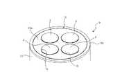
次に、本実施形態のドライエッチング装置1にて取り扱われる基板2を保持するトレイ15について、図2および図3の模式斜視図を用いて説明する。 Next, the
トレイ15は薄板円板状のトレイ本体15aを備える。トレイ15の材質としては、例えばアルミナ(Al2O3)、窒化アルミニウム(AlN)、ジルコニア(ZrO)、イットリア(Y2O3)、窒化シリコン(SiN)、炭化シリコン(SiC)等のセラミクス材や、アルマイトで被覆したアルミニウム、表面にセラミクスを溶射したアルミニウム、樹脂材料で被覆したアルミニウム等の金属がある。Cl系プロセスの場合にはアルミナ、イットリア、炭化シリコン、窒化アルミニウム等、F系プロセスの場合には石英、水晶、イットリア、炭化シリコン、アルマイトを容射したアルミニウム等を採用することが考えられる。なお、本実施形態では、炭化シリコンを主材料として形成されたトレイ15が用いられる。The
トレイ本体15aには、上面15bから下面15cまで厚み方向に貫通する4個の基板収容孔19が設けられている。基板収容孔19は、上面15b及び下面15cから見てトレイ本体15aの中心に対して等角度間隔で配置されている。図4(A)及び(B)に詳細に示すように、それぞれの基板収容孔19の内壁15dには、孔中心に向けて突出する基板支持部21が設けられている。本実施形態では、基板支持部21は内壁15dの全周に設けられており、平面視で円環状である。 The
それぞれの基板収容孔19にはそれぞれ1枚の基板2が収容される。基板収容孔19に収容された基板2は、その外周縁部2aの下面部分が基板支持部21の上面21aに支持される。また、基板収容孔19はトレイ本体15aを厚み方向に貫通するように形成されているので、トレイ本体15aの下面側から見ると、基板収容孔19により基板2の下面が露出した状態とされている。 Each
トレイ本体15aには、外周縁を部分的に切り欠いたノッチ15eが形成されており、搬送時などでトレイ15を取り扱う際に、センサ等を用いてトレイ15の向きを容易に確認できる。 The tray
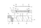
次に、図1〜図3、図4を参照して、基板ステージ9について説明する。 Next, the substrate stage 9 will be described with reference to FIGS.
図1に示すように、基板ステージ9は、セラミクス等の誘電体部材により形成されたステージ上部23と、表面にアルマイト被覆を形成したアルミニウム等により形成され、バイアス電圧が印加される下部電極として機能する金属ブロック24と、絶縁体25と、金属製のシールド27とを備える。基板ステージ9の最上部に配置されるステージ上部23は、金属ブロック24の上面に固定されており、ステージ上部23および金属ブロック24の外周が絶縁体25により覆われて、さらに絶縁体25の外周が金属により形成されたシールド27により覆われている。 As shown in FIG. 1, the substrate stage 9 is formed of a stage
図2に示すように、ステージ上部23は円板状に形成されており、ステージ上部23の上端面は、トレイ15の下面15cを支持するトレイ支持部28となっている。また、トレイ15のそれぞれの基板収容孔19と対応する短円柱状の4個の基板保持部29がトレイ支持部28から上向きに突出している。さらにステージ上部23上には、トレイ支持部28を囲むように配置され、ステージ上部23から上向きに突出して形成された環状のガイドリング30が配置されている。このガイドリング30は、ステージ上部23において、トレイ15の配置位置を案内する役目を担っている。 As shown in FIG. 2, the stage
ここで、トレイ15、基板2、および基板保持部29等の関係について、図4(A),(B)を参照して説明する。基板保持部29の外径R1は、基板支持部21の先端面(内周端面)21bの内径R2よりも小さく設定されている。したがって、トレイ15がトレイ支持部28上に配置された状態において、基板収容孔19に形成された基板支持部21と、基板保持部29との間には、互いに接触しないような隙間が確保される。 Here, the relationship among the
また、トレイ本体15aの下面15cから基板支持部21の上面21aまでの高さH1は、トレイ支持部28から基板保持部29における保持面31までの高さH2よりも低く設定されている。したがって、トレイ15の下面15cがトレイ支持部28上に配置された状態では、基板保持部29の保持面31により基板2が押し上げられ、トレイ15の基板支持部21から基板2が浮き上がった状態となる。言い換えれば、基板収容孔19に基板2を収容しているトレイ15をステージ上部23上に配置すると、基板収容孔19に収容された基板2は基板支持部21の上面21aから浮き上がり、基板2の縁部2aと基板支持部21の上面21aとが互いに離間した状態にて、基板2の下面が基板保持部29の保持面31上に配置される。なお、図3および図4(B)に示すように、それぞれの基板2が基板保持部29上に配置されて、トレイ15から離間した状態では、基板2の上面とトレイ15の上面15bとはほぼ同じ高さに位置された状態となる。 The height H1 from the
また、基板保持部29の外径R1は、基板2の外径R3よりも小さく設定されている。したがって、基板2が基板保持部29上に配置されて、トレイ15から離間した状態では、図4(B)に示すように、基板2の縁部2aが基板保持部29の外周端部より径方向外向きに突出してはみ出した状態とされる。 Further, the outer diameter R1 of the
また、図1に示すように、ステージ上部23に設けられた個々の基板保持部29の保持面31付近にはESC電極(静電吸着用電極)40が内蔵されている。これらのESC電極40は電気的に互いに絶縁されており、直流電源を内蔵するESC駆動電源部41から静電吸着用の直流電圧が印加される。 Further, as shown in FIG. 1, an ESC electrode (electrostatic chucking electrode) 40 is built in the vicinity of the holding
図1に示すように、それぞれの基板保持部29の保持面31には冷却ガス供給口44が設けられており、それぞれの冷却ガス供給口44は冷却ガス供給路47を通じて共通の冷却ガス供給部45に接続されている。なお、本実施形態では、冷却ガスとしてヘリウム(He)が用いられ、プラズマ処理中において、基板保持部29の保持面31と基板2との間に冷却ガスが供給されることで基板2の冷却が行われる。 As shown in FIG. 1, a cooling
金属ブロック24には、バイアス電圧としての高周波を印加する第2の高周波電源部56が電気的に接続されている。第2の高周波電源部56はマッチング回路を備えている。 The
また、金属ブロック24内には、金属ブロック24を冷却するための冷媒流路60が形成されており、冷却ユニット59より温度調節された冷媒が冷媒流路60に供給されることで、金属ブロック24が冷却される。 In addition, a
図1に示すように、基板ステージ9には、トレイ支持部28上に配置された状態のトレイ15をその下面側から押し上げて(突き上げて)トレイ15とともにそれぞれの基板2を上昇させる複数本のトレイ押上ロッド18が備えられている。それぞれのトレイ押上ロッド18は、トレイ支持部28の上面より突出した押上位置と、トレイ支持部28内に格納された格納位置との間で駆動機構17により昇降駆動される。 As shown in FIG. 1, the substrate stage 9 includes a plurality of
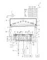
次に、ドライエッチング装置1が備える制御部70の構成について、図5に示すブロック図を用いて説明する。 Next, the configuration of the
図5に示すように、ドライエッチング装置1が備えるそれぞれの構成部である、第1の高周波電源部7、第2の高周波電源部56、ESC駆動電源部41、ゲートバルブ3a、搬送機構、駆動機構17、ガス供給部12、冷却ユニット59、および圧力制御部13の動作が他の構成部の動作と関連付けられながら統括的に制御部70により制御される。また、制御部70には、オペレータによる操作や入力を行うための操作・入力部71と、ドライエッチング装置1における運転情報などを表示する表示部72とが備えられている。 As shown in FIG. 5, the first high frequency power supply unit 7, the second high frequency
また、本実施形態のドライエッチング装置1では、基板2として例えばサファイア基板が取り扱われ、エッチング処理(プラズマ処理)として、サファイア基板2の表面に微小な凹凸構造を形成する加工(PSS:Paterned Sapphire Substrate)が行われる。なお、このように基板2の表面に微小な凹凸構造を形成する加工を基板表面の粗面化加工または表面テキスチャ加工と言うこともできる。 Further, in the
ドライエッチング装置1では、このようなエッチング処理を行うために、トレイ15に保持された複数の基板2をチャンバ3内に搬入して、基板ステージ9上に載置するトレイ搬入処理(基板搬入工程および基板載置工程)と、搬入された基板2に対してエッチング処理によりPSS加工を行うエッチング処理(第1プラズマ処理工程)と、エッチング処理の実施により基板2およびトレイ15に付着した副生成物をプラズマ処理により除去するクリーニング処理(第2プラズマ処理工程)と、除電プラズマを発生させて基板2と基板保持部29との間の残留静電吸着力を低減させる除電処理(除電工程)と、それぞれの基板2をトレイ15に保持させた状態にてチャンバ3内より搬出するトレイ搬出処理(基板搬出工程)とが予め設定されたプログラムを実行することにより連続的に実施される。そのため、制御部70には、これらのプログラムおよびプログラムを実行する演算部により構成され、各種処理を実行する処理部として、搬送処理部73、エッチング処理部74、クリーニング処理部75、および除電処理部76が備えられている。また、エッチング処理、クリーニング処理、および除電処理を実施するための各種運転条件を記憶する運転条件記憶部77が制御部70には備えられている。 In the
次に、上述したような構成を有するドライエッチング装置1を用いて、複数の基板2に対してエッチング処理を行う方法について、図6に示すフローチャートを用いて説明する。なお、以降に説明するそれぞれの処理は、ドライエッチング装置1が備える制御部70によりそれぞれの構成部が予め設定されたプログラムおよび運転条件に基づいて制御されることにより実施される。 Next, a method for performing an etching process on a plurality of
(トレイ搬入処理)
まず、図6のフローチャートにおけるトレイ搬入処理(ステップS1)を実施する。具体的には、ドライエッチング装置1において、ゲートバルブ3aを開放状態とさせる。その後、4個の基板収容孔19にそれぞれ基板2が収容された状態のトレイ15を、搬送機構のハンド部により保持して、例えばロードロック室からゲートバルブ3aを通ってチャンバ3内に搬入する。(Tray import processing)
First, the tray carry-in process (step S1) in the flowchart of FIG. 6 is performed. Specifically, in the
チャンバ3内では、駆動機構17によって駆動されたトレイ押上ロッド18が上昇し、ハンド部からトレイ押上ロッド18の上端にトレイ15が移載される。トレイ15の移載後、ハンド部はロードロック室に待避し、ゲートバルブ3aが閉鎖される。 In the
上端にトレイ15を支持したトレイ押上ロッド18は、その押上位置から基板ステージ9内に格納される格納位置に向けて降下する。トレイ15は下面15cが基板ステージ9のステージ上部23のトレイ支持部28まで降下し、トレイ15はステージ上部23のトレイ支持部28によって支持される。トレイ15がトレイ支持部28に向けて降下する際に、ステージ上部23の基板保持部29がトレイ15の対応する基板収容孔19内にトレイ15の下面15c側から進入する。トレイ15の下面15cがトレイ支持部28に当接する前に、基板保持部29の上端面である保持面31が、基板2の下面に当接する。さらにトレイ15を下降させてトレイ15の下面15cをトレイ支持部28上に載置すると、それぞれの基板2の縁部2aが基板支持部21の上面21aから持ち上げられて、トレイ15と基板2とが互いに離間した状態となる。なお、トレイ15は、ガイドリング30によりその配置位置が位置決めされるため、それぞれの基板2は基板保持部29に対して高い位置決め精度で配置される。 The tray push-up
その後、それぞれの基板保持部29に内蔵されたESC電極40に対してESC駆動電源部41から直流電圧を印加する。 Thereafter, a DC voltage is applied from the ESC drive
(エッチング処理)
次に、エッチング処理(ステップS2)を実施する。具体的には、ガス供給部12からチャンバ3内にエッチング処理用のガスが供給されるとともに、圧力制御部13によりチャンバ3内は所定圧力に調整される。続いて、第1の高周波電源部7からICPコイル5に高周波電圧を印加する。これによりチャンバ3内にプラズマが発生する。(Etching process)
Next, an etching process (step S2) is performed. Specifically, a gas for etching treatment is supplied from the
また、チャンバ3内にプラズマが発生することにより基板2と基板保持部29の間に静電吸着力が発生し、それぞれの基板保持部29の保持面31に基板2が静電吸着される。基板2の下面はトレイ15を介することなく保持面31上に直接配置されている。したがって、基板2は保持面31に対して高い密着度で保持される。その後、それぞれの基板保持部29の保持面31と基板2の下面との間に存在する空間内に、冷却ガス供給口44を通して冷却ガス供給部45から冷却ガスが供給され、この空間に冷却ガスが充填される。冷却ガスが十分に充填された状態(所定の圧力に保たれた状態)にて、第2の高周波電源部56により基板ステージ9の金属ブロック24にバイアス電圧を印加し、チャンバ3内で発生したプラズマを基板ステージ9側へ引き寄せる。これにより、基板2に対するエッチング処理が行われて、基板2の表面に対するPSS加工が実施される。1枚のトレイ15で4枚の基板2を基板ステージ9上に載置できるので、バッチ処理が可能である。 Further, when plasma is generated in the
エッチング処理中は、冷却ガスによる冷却に加えて、冷却ユニット59によって冷媒流路60中で冷媒を循環させて金属ブロック24を冷却し、それによってステージ上部23及び保持面31に保持された基板2が冷却される。したがって、エッチング処理において、基板2の温度が確実に制御される。所定の処理時間経過すると、第2の高周波電源部56による基板ステージ9の金属ブロック24へのバイアス電圧の印加を停止するとともに、エッチング処理用のガスの供給を停止して、基板2に対するエッチング処理が完了する。 During the etching process, in addition to cooling with the cooling gas, the cooling
(クリーニング処理)
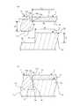
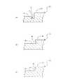
ここで、このようなエッチング処理が行われた直後の基板2およびトレイ15の状態を図7Aおよび図7Bの説明図に示す。図7Aに示すように、トレイ支持部28上にトレイ15が載置され、それぞれの基板保持部29上に基板2が保持されている状態では、トレイ15の基板支持部21の上面21aと基板2の縁部2aの下面との間には、互いに接触しないような隙間が設けられている。このような状態にてエッチング処理が行われると、基板2の縁部2aの下面やその近傍(部分A)、基板2の縁部2aにて隠れてしまっているトレイ15の基板支持部21の上面21aおよびその近傍部分(部分B)では、エッチング処理の際に生じる副生成物であるデポ(デポジション(堆積物))が付着し易い。なお、図中参照符号91は生成されたプラズマ、92はシース、93は付着したデポを模式的に示したものである。(Cleaning process)
Here, the state of the
特に、トレイ15を用いて複数の基板2を支持しながら搬送を行うという形態では、基板2の縁部2aをトレイ15の基板支持部21に支持させる必要があるため、基板2を基板保持部29上に配置した状態にて、基板保持部29の外周端部よりも基板2の縁部2aがはみ出すような状態となる。さらに、基板2の縁部2aとトレイ15の基板支持部21とは互いに離間した状態にてエッチング処理が行われることになる。そのため、エッチング処理の際に、生成されたプラズマが比較的侵入し難い部位である基板2の縁部2aの下面やトレイ15の基板支持部21等にエッチング処理の副生成物であるデポ93が付着して残り易くなる。このように基板2とトレイ15との間に付着したデポ93を除去する処理が次のクリーニング処理である。 In particular, in the form of transporting while supporting a plurality of
エッチング処理が完了し、バイアス電圧の印加およびエッチング処理用のガスの供給が停止された後、クリーニング処理を実施する(ステップS3)。具体的には、ガス供給部12からチャンバ3内にエッチング処理用のガスとは異なる種類のクリーニング処理用のガスが供給されるとともに、圧力制御部13によりチャンバ3内を所定圧力に調整する。続いて、第1の高周波電源部7からICPコイル5に高周波電圧を印加してチャンバ3内にプラズマを発生させる。この際、第2の高周波電源部56によるバイアス電圧は印加しない。このプラズマにより基板2の縁部2aおよびトレイ15の基板支持部21ならびにその近傍に付着しているデポが除去される。 After the etching process is completed and the application of the bias voltage and the supply of the etching process gas are stopped, a cleaning process is performed (step S3). Specifically, a cleaning gas of a different type from the etching gas is supplied from the
ここで、基板2の縁部2aの下面とトレイ15の基板支持部21との間の隙間の奥側には、基板保持部29の側面26が位置している。この隙間は、縁部2aの下面と基板支持部21とが互いに接触しない程度の隙間として設けられているため、隙間の奥側に位置する基板保持部29の側面26は、クリーニング処理時に生成されるプラズマに曝されにくい。そのため、クリーニング処理により除去されたデポの多くを、基板保持部29の側面26に付着して堆積させることができる。さらに、クリーニング処理を繰り返すと、デポを重ねて集積させることができる。すなわち、クリーニング処理により除去されたデポを、側面26に局所的に集積させることができ、このようなデポの集積作用を利用することで、連続運転後のメンテナンス時などにおいて、例えば側面26に対して重点的に拭き取りなどを行うことにより、効率的なメンテナンス作業を実施することができる。 Here, the
このクリーニング処理では、チャンバ3内の圧力は、エッチング処理における圧力よりも高い圧力に調整される。このようにクリーニング処理において、チャンバ3内の空間を高い圧力とすることにより、生成されるプラズマの等方性的な特性を強めることができ、基板2の縁部2aとトレイ15の基板支持部21との間の隙間にプラズマをより侵入させ易くすることができ、付着しているデポを効果的に除去できる。また、生成されるプラズマを上記隙間へ侵入させやすくするために、第2の高周波電源部56により金属ブロック24にバイアス電圧を印加してもよい。この場合、クリーニング処理中に印加するバイアス電圧はエッチング処理中におけるバイアス電圧よりも低くすることが望ましい。 In this cleaning process, the pressure in the
また、クリーニング処理では、ESC駆動電源部41からESC電極40に対して印加される直流電圧を、エッチング処理中に印加される直流電圧よりも低くすることが望ましい。上述したようにクリーニング処理では、チャンバ3内の圧力を高めることなどによりプラズマの等方性的な特性を強めるようにしている。そのため、基板2の縁部2aとトレイ15の基板支持部21との間の隙間にプラズマが侵入することにより、基板保持部29の近傍に電子が多く存在することになる。一方、基板保持部29を含むステージ上部23を構成する誘電体部材には、基板保持部29の保持面31における静電吸着力を確保するために低抵抗型のセラミックス(体積抵抗率(25℃)が1010〜1011Ω・cm)が使用されている。このため、基板保持部29の近傍に電子が多く存在する状態でエッチング処理の場合と同等の電圧をESC電極40に印加すると絶縁破壊を生じるおそれがある。そこで、クリーニング処理を行う際には、基板保持部29に内蔵されるESC電極40に印加される直流電圧をエッチング処理の場合に印加する電圧よりも低くするかゼロとすることにより、ESC電極40の周囲に絶縁破壊が生じることを防止している。In the cleaning process, it is desirable that the DC voltage applied from the ESC drive
また、クリーニング処理においては、このようにESC電極40への印加電圧が下げられているため、基板2に対する静電吸着力も下がることになる。そのため、冷却ガス供給部45から供給されて、基板2と基板保持部29との間に充填される冷却ガスのチャンバ内部との差圧についても、静電吸着力の大きさに応じて低く設定するか、静電吸着力の大きさに関係なくゼロに設定、すなわち冷却ガスの供給を遮断する。 In the cleaning process, since the voltage applied to the
その後、所定時間が経過すると、第2の高周波電源部56による基板ステージ9の金属ブロック24へのバイアス電圧の印加を停止するとともに、クリーニング処理用のガスの供給を停止して、基板2およびトレイ15に対するクリーニング処理が完了する。なお、クリーニング処理におけるバイアス電圧と冷却ガスの圧力の設定条件としては、両者ともゼロとする条件が最も好ましい。 Thereafter, when a predetermined time elapses, the application of the bias voltage to the
(除電処理)
続いて、残留静電吸着力を低減させるための除電処理を実施する(ステップS4)。具体的には、ガス供給部12からチャンバ3内にクリーニング処理用のガスとは異なる種類の除電処理用のガス(ArやHe等の不活性ガスやエッチングに寄与しにくいO2等のガス等。)が供給されるとともに、圧力制御部13によりチャンバ3内を所定圧力に調整する。また、ESC駆動電源部41によるESC電極40への直流電圧の印加を停止する。続いて、第1の高周波電源部7からICPコイル5に高周波電圧を印加する。このとき、印加される高周波電圧は、クリーニング処理の際に印加される電圧よりも低く設定される。この状態において、チャンバ3内に生成されたプラズマにより、基板2と基板保持部29との間に残留している静電吸着力を低減させる。なお、前述のクリーニング処理において冷却ガスを供給している場合は、除電処理に先立ち、冷却ガス供給部45からの冷却ガスの供給を停止して、基板2と基板保持部29との間に充填されている冷却ガスを抜いておく。(Static elimination process)
Subsequently, a charge removal process for reducing the residual electrostatic attraction force is performed (step S4). Specifically, the
その後、所定時間経過すると、第1の高周波電源部7によるICPコイル5への高周波電圧の印加を停止する。 Thereafter, when a predetermined time elapses, the application of the high frequency voltage to the
(トレイ搬出処理)
続いて、チャンバ3内からそれぞれの基板2をトレイ15とともに搬出するトレイ搬出処理を実施する(ステップS5)。具体的には、図8(A),(B)に示すように、駆動機構17によりそれぞれのトレイ押上ロッド18を上昇させる。トレイ押上ロッド18が上昇すると、その上端でトレイ15の下面15cが押し上げられ、ステージ上部23のトレイ支持部28からトレイ15が浮き上がる。トレイ押上ロッド18とともにトレイ15がさらに上昇すると、図8(B)に示すように、トレイ15の基板支持部21と基板2の縁部2aの下面とが接触して、それぞれの基板2がトレイ15により支持された状態にて押し上げられ、基板保持部29の保持面31から浮き上がる。(Tray unloading process)
Subsequently, a tray unloading process for unloading each
その後、ゲートバルブ3aが開放されて、搬送機構のハンド部81がチャンバ3内に挿入される。その後、図8(C),(D)に示すように、4個の基板収容孔19にそれぞれ基板2が収容された状態のトレイ15が、トレイ押上ロッド18からハンド部81に受け渡されて、ゲートバルブ3aを通して、トレイ15に支持された状態の基板2が搬出される。 Thereafter, the
なお、それぞれのトレイ押上ロッド18を用いてトレイ15を押し上げる動作は、除電用のプラズマを用いて除電処理が行われている間に、並行して実施してもよい。 The operation of pushing up the
このように本実施形態の基板2に対するエッチング処理方法によれば、基板2の縁部2aがトレイ15の基板支持部21により支持された状態でトレイ15による複数の基板2の搬送が行われ、基板2の縁部2aとトレイ15の基板支持部21とが互いに接触しない程度に離間した状態にて基板2に対するエッチング処理が行われる形態において、基板2のエッチング処理の際に基板2の縁部2aとトレイ15の基板支持部21とに付着した副生成物であるデポを、このエッチング処理に続けてクリーニング処理を実施することにより、生成されたプラズマを用いて効果的に除去することができる。 As described above, according to the etching method for the
よって、その後、トレイ15の基板支持部21に基板2の縁部2aを再び支持させて、トレイ15に収容させた状態にて複数の基板2をチャンバ3から搬出する際に、トレイ15と基板2との接触によりデポが落下することを防止することができる。したがって、このようなデポが基板保持部29上等に落下して、次の処理を行う際にコンタミネーションが生じることなどのトラブルの発生を回避することができ、基板のエッチング処理方法における製品の品質を向上させることができる。 Therefore, after that, when the plurality of
特に、このようなトレイ15を用いて基板2が取り扱われる形態では、エッチング処理が行われる際に、基板2の縁部2aとトレイ15の基板支持部21との間は、生成されたプラズマが侵入し難いように設定することが好ましい。一方、この隙間に侵入して基板2の縁部2aおよびトレイ15の基板支持部21の表面に付着したデポを、クリーニング処理の実施により除去するためには、生成されたプラズマをこの隙間に効果的に侵入させる必要がある。本実施形態では、クリーニング処理にて生成されるプラズマの等方性的な特性を高めることにより、この隙間にプラズマを効果的に侵入させて付着したデポの除去を行うことができる。 In particular, in the form in which the
なお、エッチング処理中にプラズマが基板2の下面側に侵入するのを防止するためには、基板2の縁部2aとトレイ15の基板収容孔19の内壁15dとの間の隙間が0.1〜0.2mm程度、基板2の縁部2aの下面とトレイ15の基板支持部21の上面21aとの間の隙間が0.2〜0.3mm程度、基板保持部29の側壁と基板支持部21の先端(内壁端)との隙間が0.5mm程度であることが好ましい。 In order to prevent plasma from entering the lower surface side of the
また、本実施形態のエッチング処理方法において、基板2としてサファイア基板を用いて処理を行う場合には、それぞれの処理の運転条件は、次のように設定することができる。これらの運転条件は、制御部70の運転条件記憶部77に予め記憶されている。なお、これらの運転条件は一例であり、処理される基板の種類や処理内容などにより最適な条件に設定することができる。 Moreover, in the etching processing method of this embodiment, when processing is performed using a sapphire substrate as the
エッチング処理:
処理ガス種・流量: BCl3、200cc
処理圧力: 0.6Pa
ICPコイル印加パワー: 1400W
バイアス: 1600W
ESC電極への印加電圧: 2.0kV
冷却ガス圧力: 2.0kPa
処理時間: 10minEtching process:
Process gas type and flow rate: BCl3 , 200cc
Processing pressure: 0.6Pa
ICP coil applied power: 1400W
Bias: 1600W
Applied voltage to ESC electrode: 2.0 kV
Cooling gas pressure: 2.0 kPa
Processing time: 10min
クリーニング処理:
処理ガス種・流量: O2、200cc/CF4、200cc
処理圧力: 8.0Pa
ICPコイル印加パワー: 1800W
バイアス: 0W
ESC電極への印加電圧: 1.0kV
冷却ガス圧力: 1.0kPa
処理時間: 2minCleaning process:
Process gas type / flow rate: O2 , 200 cc / CF4 , 200 cc
Processing pressure: 8.0 Pa
ICP coil applied power: 1800W
Bias: 0W
Applied voltage to ESC electrode: 1.0 kV
Cooling gas pressure: 1.0 kPa
Processing time: 2min
除電処理:
処理ガス種・流量: Ar、200cc
処理圧力: 8.0Pa
ICPコイル印加パワー: 200W
バイアス: 0W
ESC電極への印加電圧: 0kV
冷却ガス圧力: 0kPa
処理時間: 10secStatic elimination treatment:
Process gas type and flow rate: Ar, 200cc
Processing pressure: 8.0 Pa
ICP coil applied power: 200W
Bias: 0W
Applied voltage to ESC electrode: 0 kV
Cooling gas pressure: 0 kPa
Processing time: 10 sec
基板2の縁部2aの下面とトレイ15の基板支持部21との間の隙間により、基板保持部29の側面26はクリーニング処理のプラズマに曝されにくいので、クリーニング処理により除去されたデポの多くを、側面26に付着して堆積させることができる。すなわち、クリーニング処理により除去されたデポを、側面26に局所的に集積させることができ、このようなデポの集積作用を利用することで、連続運転後のメンテナンス時などにおいて、例えば側面26に対して重点的に拭き取りなどを行うことにより、効率的なメンテナンス作業を実施することができる。 Because of the gap between the lower surface of the
ここで、クリーニング処理の実施による側面26へのデポの集積効果を、より効果的に利用するような幾つかの変形例について、図9、10を用いて説明する。 Here, some modified examples that more effectively use the deposit accumulation effect on the
(変形例1)
図9は、変形例1によるステージ上部23における基板保持部29の側面26の近傍を示す部分断面図である。図9(A)に示すように、基板保持部29の外周には、環状の溝32が形成されている。このような構成では、溝32が形成されていることにより側面26の面積を拡大することができるため、側面26に、より多くのデポを付着して堆積させることができる。したがって、メンテナンス作業をより効率的なものにすることができる。(Modification 1)
FIG. 9 is a partial cross-sectional view showing the vicinity of the
側面の面積を拡大させるような構成は、図9(A)の構成に限られない。例えば、図9(B)に示すように、側面26が傾斜面として形成されても良い。また、この場合の傾斜方向はどちら向きでも良い。 The configuration for expanding the area of the side surface is not limited to the configuration in FIG. For example, as shown in FIG. 9B, the
あるいは、デポを集積させた後にデポの拭き取り作業を円滑に行うために、図9(C)に示すように、側面26とトレイ支持部28との境界部分に、曲面部33を形成しても良い。 Alternatively, a curved surface portion 33 may be formed at the boundary portion between the
(変形例2)
上記実施形態では、トレイ15がトレイ支持部28上に載置された状態にてクリーニング処理が実施されるような場合を例として説明したが、図10(A)、(B)に示すように、クリーニング処理中において、トレイ押上ロッド18によりトレイ15の突き上げ動作を行い、トレイ15をトレイ支持部28より離間させた状態とさせても良い。このようにクリーニング処理中に突き上げ動作を行うことにより、クリーニング効果と側面26へのデポの再付着による集積効果とのバランスを考慮して、基板2の縁部2aの下面とトレイ15の基板支持部21との間の隙間の大きさを制御することができ、効率的なクリーニング処理を実現できる。(Modification 2)
In the above embodiment, the case where the cleaning process is performed in a state where the
なお、本発明は上述の構成に限定されるものではなく、その他種々の態様で実施できる。例えば、サファイア基板に代えて、シリコン基板に対しても本実施形態のエッチング処理方法を適用できる。 In addition, this invention is not limited to the above-mentioned structure, It can implement in another various aspect. For example, the etching method of this embodiment can be applied to a silicon substrate instead of a sapphire substrate.
さらに円盤状の基板に代えて、四角形状の基板に対しても本実施形態のエッチング処理方法を適用できる。このような四角形状基板としては、例えば、太陽光パネル基板がある。太陽光パネル基板では、太陽光を効率的に吸収するために基板の表面に微小な凹凸構造がエッチング処理や表面テキスチャ加工により形成され、凹凸構造がエッチング処理により形成される点においてはサファイア基板と共通する。また、このような太陽光パネル基板では、シリコン系材料により形成されるものが多く、また、トレイを用いた基板の搬送が採用されている。 Furthermore, the etching processing method of this embodiment can be applied to a quadrangular substrate instead of the disc-shaped substrate. An example of such a rectangular substrate is a solar panel substrate. In the solar panel substrate, in order to efficiently absorb sunlight, a minute concavo-convex structure is formed on the surface of the substrate by etching treatment or surface texture processing, and in that the concavo-convex structure is formed by etching treatment, Common. In addition, such solar panel substrates are often formed of a silicon-based material, and substrate transport using a tray is employed.
また、上述の構成では、トレイ15の基板収容孔19の内壁の全周囲に渡って形成された基板支持部21により、基板2の縁部2aの全周囲が支持されるような例について説明したが、基板支持部21が基板収容孔19の内壁の一部について形成されて、基板2の縁部2aがその外周の一部において支持されるような構成を採用しても良い。 Further, in the above-described configuration, the example in which the entire periphery of the
また、基板2と基板保持部29との間に残留する静電吸着力の大きさが低い場合等には、除電処理を実施しないようにすることもできる。 Further, when the magnitude of the electrostatic attraction force remaining between the
また、本実施形態のエッチング処理方法を複数枚のトレイ15に対して連続的に実施した後、チャンバ3内にトレイ15を載置しない状態にてクリーニング処理を実施して、チャンバ3内に付着しているデポを除去するようにしても良い。 In addition, after the etching processing method of the present embodiment is continuously performed on a plurality of
また、基板保持部29の側壁を傾斜させるように構成することで、デポを付着し難くすることもできる。 In addition, it is possible to make it difficult to attach the deposit by configuring the side wall of the
なお、上記様々な実施形態のうちの任意の実施形態を適宜組み合わせることにより、それぞれの有する効果を奏するようにすることができる。 It is to be noted that, by appropriately combining arbitrary embodiments of the various embodiments described above, the effects possessed by them can be produced.
本発明は、トレイに収容された状態で搬送が行われる複数の基板に対してプラズマ処理を行う方法に有用であり、特に、基板表面に微小な凹凸構造を形成する基板の粗面化処理や表面テキスチャ加工をエッチング処理により行うような方法に適用できる。 INDUSTRIAL APPLICABILITY The present invention is useful for a method of performing plasma processing on a plurality of substrates that are transported in a state of being accommodated in a tray, and in particular, a roughening treatment of a substrate that forms a minute uneven structure on the substrate surface, It can be applied to a method in which surface texture processing is performed by etching.
1 ドライエッチング装置
2 基板
2a 縁部
3 チャンバ
3a ゲートバルブ
4 天板
5 ICPコイル
6 天板カバー部
7 第1の高周波電源部
9 基板ステージ
10 コイルカバー部
12 ガス供給部
13 圧力制御部
15 トレイ
15a トレイ本体
17 駆動機構
18 トレイ押上ロッド
19 基板収容孔
21 基板支持部
23 ステージ上部
24 金属ブロック
25 絶縁体
26 側面
28 トレイ支持部
29 基板保持部
30 ガイドリング
31 保持面
32 溝
33 曲面部
40 ESC電極
41 ESC駆動電源部
45 冷却ガス供給部
56 第2の高周波電源部
59 冷却ユニット
70 制御部
71 操作・入力部
72 表示部
73 搬送処理部
74 エッチング処理部
75 クリーニング処理部
76 除電処理部
77 運転条件記憶部DESCRIPTION OF
Claims (7)
Translated fromJapaneseチャンバ内において、トレイ支持部とこのトレイ支持部から上向きに突出する複数の基板保持部とを有する基板ステージに対して、トレイ支持部上にトレイを載置するとともにそれぞれの基板保持部上に基板を載置することで、基板保持部の端縁よりはみ出した基板の縁部と基板支持部とを離間させた状態とする基板載置工程と、
チャンバ内へ処理ガスを供給すると共にチャンバ内の圧力を調整して、それぞれの基板に対するプラズマ処理を行う第1プラズマ処理工程と、
トレイおよびそれぞれの基板が基板ステージ上に載置された状態にて、チャンバ内へ処理ガスを供給すると共にチャンバ内の圧力を調整してプラズマ処理を実施し、第1プラズマ処理工程の実施により基板の縁部と基板支持部とに付着した副生成物を除去する第2プラズマ処理工程と、
第2プラズマ処理工程の終了後、基板支持部により基板の縁部を支持した状態にて、トレイとともにそれぞれの基板をチャンバ内より搬出する基板搬出工程と、を含み、
第1プラズマ処理工程において、それぞれの基板を静電吸着により基板保持部に吸着保持するとともに、基板と基板保持部の間に所定の圧力で供給される冷却ガスにより冷却しながら、プラズマ処理を行い、
第1プラズマ処理工程の終了後、第2プラズマ処理工程を実施する際に、第1プラズマ処理工程における静電吸着の駆動電圧よりも低い駆動電圧に切り換えて静電吸着を行うとともに、第1プラズマ処理工程における処理ガスとは異なる種類の処理ガスに切り換えて、第1プラズマ処理工程における圧力よりも高い圧力にて第2プラズマ処理工程を行う、基板のプラズマ処理方法。A plurality of substrate accommodation holes for accommodating the substrate are provided, and a tray having a substrate support portion protruding from the inner wall of the substrate accommodation hole is used, and the edge portion is supported by the substrate support portion and accommodated in the substrate accommodation hole. A substrate carrying-in step of carrying a plurality of substrates in a state of being brought into the chamber;
In a chamber, with respect to a substrate stage having a tray support portion and a plurality of substrate holding portions protruding upward from the tray support portion, a tray is placed on the tray support portion and a substrate is placed on each substrate holding portion. A substrate placing step in which the edge of the substrate protruding from the edge of the substrate holding portion and the substrate support portion are separated from each other,
A first plasma processing step of supplying a processing gas into the chamber and adjusting a pressure in the chamber to perform plasma processing on each substrate;
In a state where the tray and each substrate are placed on the substrate stage, the processing gas is supplied into the chamber and the pressure in the chamber is adjusted to perform the plasma processing, and the substrate is obtained by performing the first plasma processing step. A second plasma treatment step of removing by-products attached to the edge of the substrate and the substrate support;
After completion of the second plasma treatment step, the edge of the substrate by the support state by the substrate supporting portion,seen including a substrate unloading step of unloading from the chamber of each of the substrate with the tray,and
In the first plasma processing step, each substrate is attracted and held on the substrate holding portion by electrostatic attraction, and plasma processing is performed while cooling with a cooling gas supplied at a predetermined pressure between the substrate and the substrate holding portion. ,
When the second plasma processing step is performed after the first plasma processing step is completed, electrostatic adsorption is performed by switching to a driving voltage lower than the electrostatic adsorption driving voltage in the first plasma processing step. A substrate plasma processing method, whereinthe second plasma processing step is performed at a pressure higher than the pressure in the first plasma processing step by switching to a processing gas of a different type from the processing gas in the processing step .
第2プラズマ処理工程における処理ガスとしてO2/CF4を用いる、請求項4に記載の基板のプラズマ処理方法。BCl3 is used as a processing gas in the first plasma processing step,
Using O2 / CF4 as a process gas in the second plasma treatment step, a plasma treatment method for a substrate according to claim4.
Priority Applications (4)
| Application Number | Priority Date | Filing Date | Title |
|---|---|---|---|
| JP2011014335AJP5638405B2 (en) | 2010-10-08 | 2011-01-26 | Substrate plasma processing method |
| US13/823,955US9073385B2 (en) | 2010-10-08 | 2011-09-29 | Plasma processing method for substrates |
| CN201180048666.9ACN103155117B (en) | 2010-10-08 | 2011-09-29 | The method of plasma processing of substrate |
| PCT/JP2011/005501WO2012046418A1 (en) | 2010-10-08 | 2011-09-29 | Substrate plasma treatment method |
Applications Claiming Priority (3)
| Application Number | Priority Date | Filing Date | Title |
|---|---|---|---|
| JP2010228621 | 2010-10-08 | ||
| JP2010228621 | 2010-10-08 | ||
| JP2011014335AJP5638405B2 (en) | 2010-10-08 | 2011-01-26 | Substrate plasma processing method |
Publications (2)
| Publication Number | Publication Date |
|---|---|
| JP2012099781A JP2012099781A (en) | 2012-05-24 |
| JP5638405B2true JP5638405B2 (en) | 2014-12-10 |
Family
ID=45927425
Family Applications (1)
| Application Number | Title | Priority Date | Filing Date |
|---|---|---|---|
| JP2011014335AActiveJP5638405B2 (en) | 2010-10-08 | 2011-01-26 | Substrate plasma processing method |
Country Status (4)
| Country | Link |
|---|---|
| US (1) | US9073385B2 (en) |
| JP (1) | JP5638405B2 (en) |
| CN (1) | CN103155117B (en) |
| WO (1) | WO2012046418A1 (en) |
Cited By (1)
| Publication number | Priority date | Publication date | Assignee | Title |
|---|---|---|---|---|
| JP3398670B1 (en) | 2001-11-28 | 2003-04-21 | 弘一 菅原 | Non-pneumatic tires, rim and tire assemblies and vehicles |
Families Citing this family (332)
| Publication number | Priority date | Publication date | Assignee | Title |
|---|---|---|---|---|
| US9394608B2 (en) | 2009-04-06 | 2016-07-19 | Asm America, Inc. | Semiconductor processing reactor and components thereof |
| US8802201B2 (en) | 2009-08-14 | 2014-08-12 | Asm America, Inc. | Systems and methods for thin-film deposition of metal oxides using excited nitrogen-oxygen species |
| JP5351877B2 (en)* | 2010-12-15 | 2013-11-27 | パナソニック株式会社 | Substrate plasma processing method |
| US9312155B2 (en) | 2011-06-06 | 2016-04-12 | Asm Japan K.K. | High-throughput semiconductor-processing apparatus equipped with multiple dual-chamber modules |
| US10854498B2 (en) | 2011-07-15 | 2020-12-01 | Asm Ip Holding B.V. | Wafer-supporting device and method for producing same |
| US20130023129A1 (en) | 2011-07-20 | 2013-01-24 | Asm America, Inc. | Pressure transmitter for a semiconductor processing environment |
| US9017481B1 (en) | 2011-10-28 | 2015-04-28 | Asm America, Inc. | Process feed management for semiconductor substrate processing |
| JP2013254903A (en)* | 2012-06-08 | 2013-12-19 | Panasonic Corp | Method for plasma processing of substrate |
| US10714315B2 (en) | 2012-10-12 | 2020-07-14 | Asm Ip Holdings B.V. | Semiconductor reaction chamber showerhead |
| US20160376700A1 (en) | 2013-02-01 | 2016-12-29 | Asm Ip Holding B.V. | System for treatment of deposition reactor |
| JP6273188B2 (en)* | 2013-10-31 | 2018-01-31 | 東京エレクトロン株式会社 | Plasma processing method |
| US10683571B2 (en) | 2014-02-25 | 2020-06-16 | Asm Ip Holding B.V. | Gas supply manifold and method of supplying gases to chamber using same |
| US10167557B2 (en) | 2014-03-18 | 2019-01-01 | Asm Ip Holding B.V. | Gas distribution system, reactor including the system, and methods of using the same |
| US11015245B2 (en)* | 2014-03-19 | 2021-05-25 | Asm Ip Holding B.V. | Gas-phase reactor and system having exhaust plenum and components thereof |
| US20150267295A1 (en)* | 2014-03-19 | 2015-09-24 | Asm Ip Holding B.V. | Removable substrate tray and assembly and reactor including same |
| US9410249B2 (en) | 2014-05-15 | 2016-08-09 | Infineon Technologies Ag | Wafer releasing |
| JP6377975B2 (en)* | 2014-06-23 | 2018-08-22 | 新光電気工業株式会社 | Substrate fixing device |
| US10858737B2 (en) | 2014-07-28 | 2020-12-08 | Asm Ip Holding B.V. | Showerhead assembly and components thereof |
| US9890456B2 (en) | 2014-08-21 | 2018-02-13 | Asm Ip Holding B.V. | Method and system for in situ formation of gas-phase compounds |
| US9657845B2 (en) | 2014-10-07 | 2017-05-23 | Asm Ip Holding B.V. | Variable conductance gas distribution apparatus and method |
| US10941490B2 (en) | 2014-10-07 | 2021-03-09 | Asm Ip Holding B.V. | Multiple temperature range susceptor, assembly, reactor and system including the susceptor, and methods of using the same |
| CN105576101B (en)* | 2014-10-10 | 2018-07-06 | 北京北方华创微电子装备有限公司 | A kind of cover board and bogey |
| US10648079B2 (en)* | 2014-12-19 | 2020-05-12 | Lam Research Corporation | Reducing backside deposition at wafer edge |
| TW201639063A (en)* | 2015-01-22 | 2016-11-01 | 應用材料股份有限公司 | Batch heating and cooling chamber or loadlock |
| US10276355B2 (en) | 2015-03-12 | 2019-04-30 | Asm Ip Holding B.V. | Multi-zone reactor, system including the reactor, and method of using the same |
| US10458018B2 (en) | 2015-06-26 | 2019-10-29 | Asm Ip Holding B.V. | Structures including metal carbide material, devices including the structures, and methods of forming same |
| US10600673B2 (en) | 2015-07-07 | 2020-03-24 | Asm Ip Holding B.V. | Magnetic susceptor to baseplate seal |
| US10211308B2 (en) | 2015-10-21 | 2019-02-19 | Asm Ip Holding B.V. | NbMC layers |
| US11139308B2 (en) | 2015-12-29 | 2021-10-05 | Asm Ip Holding B.V. | Atomic layer deposition of III-V compounds to form V-NAND devices |
| US10529554B2 (en) | 2016-02-19 | 2020-01-07 | Asm Ip Holding B.V. | Method for forming silicon nitride film selectively on sidewalls or flat surfaces of trenches |
| US10343920B2 (en) | 2016-03-18 | 2019-07-09 | Asm Ip Holding B.V. | Aligned carbon nanotubes |
| US10190213B2 (en) | 2016-04-21 | 2019-01-29 | Asm Ip Holding B.V. | Deposition of metal borides |
| US10865475B2 (en) | 2016-04-21 | 2020-12-15 | Asm Ip Holding B.V. | Deposition of metal borides and silicides |
| US10367080B2 (en) | 2016-05-02 | 2019-07-30 | Asm Ip Holding B.V. | Method of forming a germanium oxynitride film |
| US10032628B2 (en) | 2016-05-02 | 2018-07-24 | Asm Ip Holding B.V. | Source/drain performance through conformal solid state doping |
| US11453943B2 (en) | 2016-05-25 | 2022-09-27 | Asm Ip Holding B.V. | Method for forming carbon-containing silicon/metal oxide or nitride film by ALD using silicon precursor and hydrocarbon precursor |
| US9859151B1 (en) | 2016-07-08 | 2018-01-02 | Asm Ip Holding B.V. | Selective film deposition method to form air gaps |
| US10612137B2 (en) | 2016-07-08 | 2020-04-07 | Asm Ip Holdings B.V. | Organic reactants for atomic layer deposition |
| US10714385B2 (en) | 2016-07-19 | 2020-07-14 | Asm Ip Holding B.V. | Selective deposition of tungsten |
| KR102532607B1 (en) | 2016-07-28 | 2023-05-15 | 에이에스엠 아이피 홀딩 비.브이. | Substrate processing apparatus and method of operating the same |
| US9812320B1 (en) | 2016-07-28 | 2017-11-07 | Asm Ip Holding B.V. | Method and apparatus for filling a gap |
| US9887082B1 (en) | 2016-07-28 | 2018-02-06 | Asm Ip Holding B.V. | Method and apparatus for filling a gap |
| US10643826B2 (en) | 2016-10-26 | 2020-05-05 | Asm Ip Holdings B.V. | Methods for thermally calibrating reaction chambers |
| US11532757B2 (en) | 2016-10-27 | 2022-12-20 | Asm Ip Holding B.V. | Deposition of charge trapping layers |
| US10714350B2 (en) | 2016-11-01 | 2020-07-14 | ASM IP Holdings, B.V. | Methods for forming a transition metal niobium nitride film on a substrate by atomic layer deposition and related semiconductor device structures |
| US10229833B2 (en) | 2016-11-01 | 2019-03-12 | Asm Ip Holding B.V. | Methods for forming a transition metal nitride film on a substrate by atomic layer deposition and related semiconductor device structures |
| US10643904B2 (en) | 2016-11-01 | 2020-05-05 | Asm Ip Holdings B.V. | Methods for forming a semiconductor device and related semiconductor device structures |
| US10134757B2 (en) | 2016-11-07 | 2018-11-20 | Asm Ip Holding B.V. | Method of processing a substrate and a device manufactured by using the method |
| KR102546317B1 (en) | 2016-11-15 | 2023-06-21 | 에이에스엠 아이피 홀딩 비.브이. | Gas supply unit and substrate processing apparatus including the same |
| KR102762543B1 (en) | 2016-12-14 | 2025-02-05 | 에이에스엠 아이피 홀딩 비.브이. | Substrate processing apparatus |
| US11581186B2 (en) | 2016-12-15 | 2023-02-14 | Asm Ip Holding B.V. | Sequential infiltration synthesis apparatus |
| US11447861B2 (en) | 2016-12-15 | 2022-09-20 | Asm Ip Holding B.V. | Sequential infiltration synthesis apparatus and a method of forming a patterned structure |
| KR102700194B1 (en) | 2016-12-19 | 2024-08-28 | 에이에스엠 아이피 홀딩 비.브이. | Substrate processing apparatus |
| US10269558B2 (en) | 2016-12-22 | 2019-04-23 | Asm Ip Holding B.V. | Method of forming a structure on a substrate |
| US10867788B2 (en) | 2016-12-28 | 2020-12-15 | Asm Ip Holding B.V. | Method of forming a structure on a substrate |
| US11390950B2 (en) | 2017-01-10 | 2022-07-19 | Asm Ip Holding B.V. | Reactor system and method to reduce residue buildup during a film deposition process |
| CN108335978B (en)* | 2017-01-20 | 2022-08-26 | 东京毅力科创株式会社 | Plasma processing apparatus |
| US10655221B2 (en) | 2017-02-09 | 2020-05-19 | Asm Ip Holding B.V. | Method for depositing oxide film by thermal ALD and PEALD |
| US10468261B2 (en) | 2017-02-15 | 2019-11-05 | Asm Ip Holding B.V. | Methods for forming a metallic film on a substrate by cyclical deposition and related semiconductor device structures |
| US10529563B2 (en) | 2017-03-29 | 2020-01-07 | Asm Ip Holdings B.V. | Method for forming doped metal oxide films on a substrate by cyclical deposition and related semiconductor device structures |
| USD876504S1 (en) | 2017-04-03 | 2020-02-25 | Asm Ip Holding B.V. | Exhaust flow control ring for semiconductor deposition apparatus |
| KR102457289B1 (en) | 2017-04-25 | 2022-10-21 | 에이에스엠 아이피 홀딩 비.브이. | Method for depositing a thin film and manufacturing a semiconductor device |
| US10892156B2 (en) | 2017-05-08 | 2021-01-12 | Asm Ip Holding B.V. | Methods for forming a silicon nitride film on a substrate and related semiconductor device structures |
| US10770286B2 (en) | 2017-05-08 | 2020-09-08 | Asm Ip Holdings B.V. | Methods for selectively forming a silicon nitride film on a substrate and related semiconductor device structures |
| US12040200B2 (en) | 2017-06-20 | 2024-07-16 | Asm Ip Holding B.V. | Semiconductor processing apparatus and methods for calibrating a semiconductor processing apparatus |
| US11306395B2 (en) | 2017-06-28 | 2022-04-19 | Asm Ip Holding B.V. | Methods for depositing a transition metal nitride film on a substrate by atomic layer deposition and related deposition apparatus |
| US10685834B2 (en) | 2017-07-05 | 2020-06-16 | Asm Ip Holdings B.V. | Methods for forming a silicon germanium tin layer and related semiconductor device structures |
| KR20190009245A (en) | 2017-07-18 | 2019-01-28 | 에이에스엠 아이피 홀딩 비.브이. | Methods for forming a semiconductor device structure and related semiconductor device structures |
| US10541333B2 (en) | 2017-07-19 | 2020-01-21 | Asm Ip Holding B.V. | Method for depositing a group IV semiconductor and related semiconductor device structures |
| US11374112B2 (en) | 2017-07-19 | 2022-06-28 | Asm Ip Holding B.V. | Method for depositing a group IV semiconductor and related semiconductor device structures |
| US11018002B2 (en) | 2017-07-19 | 2021-05-25 | Asm Ip Holding B.V. | Method for selectively depositing a Group IV semiconductor and related semiconductor device structures |
| US10590535B2 (en) | 2017-07-26 | 2020-03-17 | Asm Ip Holdings B.V. | Chemical treatment, deposition and/or infiltration apparatus and method for using the same |
| TWI815813B (en) | 2017-08-04 | 2023-09-21 | 荷蘭商Asm智慧財產控股公司 | Showerhead assembly for distributing a gas within a reaction chamber |
| US10692741B2 (en) | 2017-08-08 | 2020-06-23 | Asm Ip Holdings B.V. | Radiation shield |
| US10770336B2 (en) | 2017-08-08 | 2020-09-08 | Asm Ip Holding B.V. | Substrate lift mechanism and reactor including same |
| US11769682B2 (en) | 2017-08-09 | 2023-09-26 | Asm Ip Holding B.V. | Storage apparatus for storing cassettes for substrates and processing apparatus equipped therewith |
| US11139191B2 (en) | 2017-08-09 | 2021-10-05 | Asm Ip Holding B.V. | Storage apparatus for storing cassettes for substrates and processing apparatus equipped therewith |
| US10249524B2 (en) | 2017-08-09 | 2019-04-02 | Asm Ip Holding B.V. | Cassette holder assembly for a substrate cassette and holding member for use in such assembly |
| USD900036S1 (en) | 2017-08-24 | 2020-10-27 | Asm Ip Holding B.V. | Heater electrical connector and adapter |
| US11830730B2 (en) | 2017-08-29 | 2023-11-28 | Asm Ip Holding B.V. | Layer forming method and apparatus |
| US11056344B2 (en) | 2017-08-30 | 2021-07-06 | Asm Ip Holding B.V. | Layer forming method |
| US11295980B2 (en) | 2017-08-30 | 2022-04-05 | Asm Ip Holding B.V. | Methods for depositing a molybdenum metal film over a dielectric surface of a substrate by a cyclical deposition process and related semiconductor device structures |
| KR102491945B1 (en) | 2017-08-30 | 2023-01-26 | 에이에스엠 아이피 홀딩 비.브이. | Substrate processing apparatus |
| KR102401446B1 (en) | 2017-08-31 | 2022-05-24 | 에이에스엠 아이피 홀딩 비.브이. | Substrate processing apparatus |
| KR102630301B1 (en) | 2017-09-21 | 2024-01-29 | 에이에스엠 아이피 홀딩 비.브이. | Method of sequential infiltration synthesis treatment of infiltrateable material and structures and devices formed using same |
| US10844484B2 (en) | 2017-09-22 | 2020-11-24 | Asm Ip Holding B.V. | Apparatus for dispensing a vapor phase reactant to a reaction chamber and related methods |
| US10658205B2 (en) | 2017-09-28 | 2020-05-19 | Asm Ip Holdings B.V. | Chemical dispensing apparatus and methods for dispensing a chemical to a reaction chamber |
| US10403504B2 (en) | 2017-10-05 | 2019-09-03 | Asm Ip Holding B.V. | Method for selectively depositing a metallic film on a substrate |
| US10319588B2 (en) | 2017-10-10 | 2019-06-11 | Asm Ip Holding B.V. | Method for depositing a metal chalcogenide on a substrate by cyclical deposition |
| US10923344B2 (en) | 2017-10-30 | 2021-02-16 | Asm Ip Holding B.V. | Methods for forming a semiconductor structure and related semiconductor structures |
| US10910262B2 (en) | 2017-11-16 | 2021-02-02 | Asm Ip Holding B.V. | Method of selectively depositing a capping layer structure on a semiconductor device structure |
| KR102443047B1 (en) | 2017-11-16 | 2022-09-14 | 에이에스엠 아이피 홀딩 비.브이. | Method of processing a substrate and a device manufactured by the same |
| US11022879B2 (en) | 2017-11-24 | 2021-06-01 | Asm Ip Holding B.V. | Method of forming an enhanced unexposed photoresist layer |
| WO2019103613A1 (en) | 2017-11-27 | 2019-05-31 | Asm Ip Holding B.V. | A storage device for storing wafer cassettes for use with a batch furnace |
| CN111344522B (en) | 2017-11-27 | 2022-04-12 | 阿斯莫Ip控股公司 | Including clean mini-environment device |
| US10872771B2 (en) | 2018-01-16 | 2020-12-22 | Asm Ip Holding B. V. | Method for depositing a material film on a substrate within a reaction chamber by a cyclical deposition process and related device structures |
| TWI799494B (en) | 2018-01-19 | 2023-04-21 | 荷蘭商Asm 智慧財產控股公司 | Deposition method |
| KR102695659B1 (en) | 2018-01-19 | 2024-08-14 | 에이에스엠 아이피 홀딩 비.브이. | Method for depositing a gap filling layer by plasma assisted deposition |
| USD903477S1 (en) | 2018-01-24 | 2020-12-01 | Asm Ip Holdings B.V. | Metal clamp |
| US11018047B2 (en) | 2018-01-25 | 2021-05-25 | Asm Ip Holding B.V. | Hybrid lift pin |
| USD880437S1 (en) | 2018-02-01 | 2020-04-07 | Asm Ip Holding B.V. | Gas supply plate for semiconductor manufacturing apparatus |
| US11081345B2 (en) | 2018-02-06 | 2021-08-03 | Asm Ip Holding B.V. | Method of post-deposition treatment for silicon oxide film |
| WO2019158960A1 (en) | 2018-02-14 | 2019-08-22 | Asm Ip Holding B.V. | A method for depositing a ruthenium-containing film on a substrate by a cyclical deposition process |
| US10896820B2 (en) | 2018-02-14 | 2021-01-19 | Asm Ip Holding B.V. | Method for depositing a ruthenium-containing film on a substrate by a cyclical deposition process |
| US10731249B2 (en) | 2018-02-15 | 2020-08-04 | Asm Ip Holding B.V. | Method of forming a transition metal containing film on a substrate by a cyclical deposition process, a method for supplying a transition metal halide compound to a reaction chamber, and related vapor deposition apparatus |
| KR102636427B1 (en) | 2018-02-20 | 2024-02-13 | 에이에스엠 아이피 홀딩 비.브이. | Substrate processing method and apparatus |
| US10658181B2 (en) | 2018-02-20 | 2020-05-19 | Asm Ip Holding B.V. | Method of spacer-defined direct patterning in semiconductor fabrication |
| US10975470B2 (en) | 2018-02-23 | 2021-04-13 | Asm Ip Holding B.V. | Apparatus for detecting or monitoring for a chemical precursor in a high temperature environment |
| US11473195B2 (en) | 2018-03-01 | 2022-10-18 | Asm Ip Holding B.V. | Semiconductor processing apparatus and a method for processing a substrate |
| US11629406B2 (en) | 2018-03-09 | 2023-04-18 | Asm Ip Holding B.V. | Semiconductor processing apparatus comprising one or more pyrometers for measuring a temperature of a substrate during transfer of the substrate |
| US11114283B2 (en) | 2018-03-16 | 2021-09-07 | Asm Ip Holding B.V. | Reactor, system including the reactor, and methods of manufacturing and using same |
| KR102646467B1 (en) | 2018-03-27 | 2024-03-11 | 에이에스엠 아이피 홀딩 비.브이. | Method of forming an electrode on a substrate and a semiconductor device structure including an electrode |
| US11088002B2 (en) | 2018-03-29 | 2021-08-10 | Asm Ip Holding B.V. | Substrate rack and a substrate processing system and method |
| US11230766B2 (en) | 2018-03-29 | 2022-01-25 | Asm Ip Holding B.V. | Substrate processing apparatus and method |
| KR102501472B1 (en) | 2018-03-30 | 2023-02-20 | 에이에스엠 아이피 홀딩 비.브이. | Substrate processing method |
| KR102600229B1 (en) | 2018-04-09 | 2023-11-10 | 에이에스엠 아이피 홀딩 비.브이. | Substrate supporting device, substrate processing apparatus including the same and substrate processing method |
| TWI811348B (en) | 2018-05-08 | 2023-08-11 | 荷蘭商Asm 智慧財產控股公司 | Methods for depositing an oxide film on a substrate by a cyclical deposition process and related device structures |
| US12025484B2 (en) | 2018-05-08 | 2024-07-02 | Asm Ip Holding B.V. | Thin film forming method |
| US12272527B2 (en) | 2018-05-09 | 2025-04-08 | Asm Ip Holding B.V. | Apparatus for use with hydrogen radicals and method of using same |
| KR20190129718A (en) | 2018-05-11 | 2019-11-20 | 에이에스엠 아이피 홀딩 비.브이. | Methods for forming a doped metal carbide film on a substrate and related semiconductor device structures |
| KR102596988B1 (en) | 2018-05-28 | 2023-10-31 | 에이에스엠 아이피 홀딩 비.브이. | Method of processing a substrate and a device manufactured by the same |
| TWI840362B (en) | 2018-06-04 | 2024-05-01 | 荷蘭商Asm Ip私人控股有限公司 | Wafer handling chamber with moisture reduction |
| US11718913B2 (en) | 2018-06-04 | 2023-08-08 | Asm Ip Holding B.V. | Gas distribution system and reactor system including same |
| US11286562B2 (en) | 2018-06-08 | 2022-03-29 | Asm Ip Holding B.V. | Gas-phase chemical reactor and method of using same |
| US10797133B2 (en) | 2018-06-21 | 2020-10-06 | Asm Ip Holding B.V. | Method for depositing a phosphorus doped silicon arsenide film and related semiconductor device structures |
| KR102568797B1 (en) | 2018-06-21 | 2023-08-21 | 에이에스엠 아이피 홀딩 비.브이. | Substrate processing system |
| TWI873894B (en) | 2018-06-27 | 2025-02-21 | 荷蘭商Asm Ip私人控股有限公司 | Cyclic deposition methods for forming metal-containing material and films and structures including the metal-containing material |
| KR102854019B1 (en) | 2018-06-27 | 2025-09-02 | 에이에스엠 아이피 홀딩 비.브이. | Periodic deposition method for forming a metal-containing material and films and structures comprising the metal-containing material |
| US10612136B2 (en) | 2018-06-29 | 2020-04-07 | ASM IP Holding, B.V. | Temperature-controlled flange and reactor system including same |
| KR102686758B1 (en) | 2018-06-29 | 2024-07-18 | 에이에스엠 아이피 홀딩 비.브이. | Method for depositing a thin film and manufacturing a semiconductor device |
| US10755922B2 (en) | 2018-07-03 | 2020-08-25 | Asm Ip Holding B.V. | Method for depositing silicon-free carbon-containing film as gap-fill layer by pulse plasma-assisted deposition |
| US10388513B1 (en) | 2018-07-03 | 2019-08-20 | Asm Ip Holding B.V. | Method for depositing silicon-free carbon-containing film as gap-fill layer by pulse plasma-assisted deposition |
| US10767789B2 (en) | 2018-07-16 | 2020-09-08 | Asm Ip Holding B.V. | Diaphragm valves, valve components, and methods for forming valve components |
| US11053591B2 (en) | 2018-08-06 | 2021-07-06 | Asm Ip Holding B.V. | Multi-port gas injection system and reactor system including same |
| US10883175B2 (en) | 2018-08-09 | 2021-01-05 | Asm Ip Holding B.V. | Vertical furnace for processing substrates and a liner for use therein |
| US10829852B2 (en) | 2018-08-16 | 2020-11-10 | Asm Ip Holding B.V. | Gas distribution device for a wafer processing apparatus |
| US11430674B2 (en) | 2018-08-22 | 2022-08-30 | Asm Ip Holding B.V. | Sensor array, apparatus for dispensing a vapor phase reactant to a reaction chamber and related methods |
| US11024523B2 (en) | 2018-09-11 | 2021-06-01 | Asm Ip Holding B.V. | Substrate processing apparatus and method |
| KR102707956B1 (en) | 2018-09-11 | 2024-09-19 | 에이에스엠 아이피 홀딩 비.브이. | Method for deposition of a thin film |
| US11049751B2 (en) | 2018-09-14 | 2021-06-29 | Asm Ip Holding B.V. | Cassette supply system to store and handle cassettes and processing apparatus equipped therewith |
| CN110970344B (en) | 2018-10-01 | 2024-10-25 | Asmip控股有限公司 | Substrate holding apparatus, system comprising the same and method of using the same |
| US11232963B2 (en) | 2018-10-03 | 2022-01-25 | Asm Ip Holding B.V. | Substrate processing apparatus and method |
| KR102592699B1 (en) | 2018-10-08 | 2023-10-23 | 에이에스엠 아이피 홀딩 비.브이. | Substrate support unit and apparatuses for depositing thin film and processing the substrate including the same |
| US10847365B2 (en) | 2018-10-11 | 2020-11-24 | Asm Ip Holding B.V. | Method of forming conformal silicon carbide film by cyclic CVD |
| US20200118802A1 (en)* | 2018-10-11 | 2020-04-16 | Lin-Sheng Lu | Masking structure for a wafer supporting plate |
| US10811256B2 (en) | 2018-10-16 | 2020-10-20 | Asm Ip Holding B.V. | Method for etching a carbon-containing feature |
| KR102546322B1 (en) | 2018-10-19 | 2023-06-21 | 에이에스엠 아이피 홀딩 비.브이. | Substrate processing apparatus and substrate processing method |
| KR102605121B1 (en) | 2018-10-19 | 2023-11-23 | 에이에스엠 아이피 홀딩 비.브이. | Substrate processing apparatus and substrate processing method |
| USD948463S1 (en) | 2018-10-24 | 2022-04-12 | Asm Ip Holding B.V. | Susceptor for semiconductor substrate supporting apparatus |
| US12378665B2 (en) | 2018-10-26 | 2025-08-05 | Asm Ip Holding B.V. | High temperature coatings for a preclean and etch apparatus and related methods |
| US11087997B2 (en) | 2018-10-31 | 2021-08-10 | Asm Ip Holding B.V. | Substrate processing apparatus for processing substrates |
| KR102748291B1 (en) | 2018-11-02 | 2024-12-31 | 에이에스엠 아이피 홀딩 비.브이. | Substrate support unit and substrate processing apparatus including the same |
| US11572620B2 (en) | 2018-11-06 | 2023-02-07 | Asm Ip Holding B.V. | Methods for selectively depositing an amorphous silicon film on a substrate |
| US11031242B2 (en) | 2018-11-07 | 2021-06-08 | Asm Ip Holding B.V. | Methods for depositing a boron doped silicon germanium film |
| US10847366B2 (en) | 2018-11-16 | 2020-11-24 | Asm Ip Holding B.V. | Methods for depositing a transition metal chalcogenide film on a substrate by a cyclical deposition process |
| US10818758B2 (en) | 2018-11-16 | 2020-10-27 | Asm Ip Holding B.V. | Methods for forming a metal silicate film on a substrate in a reaction chamber and related semiconductor device structures |
| US10559458B1 (en) | 2018-11-26 | 2020-02-11 | Asm Ip Holding B.V. | Method of forming oxynitride film |
| US12040199B2 (en) | 2018-11-28 | 2024-07-16 | Asm Ip Holding B.V. | Substrate processing apparatus for processing substrates |
| US11217444B2 (en) | 2018-11-30 | 2022-01-04 | Asm Ip Holding B.V. | Method for forming an ultraviolet radiation responsive metal oxide-containing film |
| KR102636428B1 (en) | 2018-12-04 | 2024-02-13 | 에이에스엠 아이피 홀딩 비.브이. | A method for cleaning a substrate processing apparatus |
| US11158513B2 (en) | 2018-12-13 | 2021-10-26 | Asm Ip Holding B.V. | Methods for forming a rhenium-containing film on a substrate by a cyclical deposition process and related semiconductor device structures |
| CN113169110A (en) | 2018-12-14 | 2021-07-23 | 应用材料公司 | Handling and handling of double-sided devices on fragile substrates |
| TWI874340B (en) | 2018-12-14 | 2025-03-01 | 荷蘭商Asm Ip私人控股有限公司 | Method of forming device structure, structure formed by the method and system for performing the method |
| TWI866480B (en) | 2019-01-17 | 2024-12-11 | 荷蘭商Asm Ip 私人控股有限公司 | Methods of forming a transition metal containing film on a substrate by a cyclical deposition process |
| KR102727227B1 (en) | 2019-01-22 | 2024-11-07 | 에이에스엠 아이피 홀딩 비.브이. | Semiconductor processing device |
| CN111524788B (en) | 2019-02-01 | 2023-11-24 | Asm Ip私人控股有限公司 | Method for forming topologically selective films of silicon oxide |
| KR102626263B1 (en) | 2019-02-20 | 2024-01-16 | 에이에스엠 아이피 홀딩 비.브이. | Cyclical deposition method including treatment step and apparatus for same |
| TWI873122B (en) | 2019-02-20 | 2025-02-21 | 荷蘭商Asm Ip私人控股有限公司 | Method of filling a recess formed within a surface of a substrate, semiconductor structure formed according to the method, and semiconductor processing apparatus |
| TWI845607B (en) | 2019-02-20 | 2024-06-21 | 荷蘭商Asm Ip私人控股有限公司 | Cyclical deposition method and apparatus for filling a recess formed within a substrate surface |
| TWI838458B (en) | 2019-02-20 | 2024-04-11 | 荷蘭商Asm Ip私人控股有限公司 | Apparatus and methods for plug fill deposition in 3-d nand applications |
| TWI842826B (en) | 2019-02-22 | 2024-05-21 | 荷蘭商Asm Ip私人控股有限公司 | Substrate processing apparatus and method for processing substrate |
| KR102858005B1 (en) | 2019-03-08 | 2025-09-09 | 에이에스엠 아이피 홀딩 비.브이. | Method for Selective Deposition of Silicon Nitride Layer and Structure Including Selectively-Deposited Silicon Nitride Layer |
| US11742198B2 (en) | 2019-03-08 | 2023-08-29 | Asm Ip Holding B.V. | Structure including SiOCN layer and method of forming same |
| KR102782593B1 (en) | 2019-03-08 | 2025-03-14 | 에이에스엠 아이피 홀딩 비.브이. | Structure Including SiOC Layer and Method of Forming Same |
| JP2020167398A (en) | 2019-03-28 | 2020-10-08 | エーエスエム・アイピー・ホールディング・ベー・フェー | Door openers and substrate processing equipment provided with door openers |
| KR102809999B1 (en) | 2019-04-01 | 2025-05-19 | 에이에스엠 아이피 홀딩 비.브이. | Method of manufacturing semiconductor device |
| KR20200123380A (en) | 2019-04-19 | 2020-10-29 | 에이에스엠 아이피 홀딩 비.브이. | Layer forming method and apparatus |
| KR20200125453A (en) | 2019-04-24 | 2020-11-04 | 에이에스엠 아이피 홀딩 비.브이. | Gas-phase reactor system and method of using same |
| US11289326B2 (en) | 2019-05-07 | 2022-03-29 | Asm Ip Holding B.V. | Method for reforming amorphous carbon polymer film |
| KR20200130121A (en) | 2019-05-07 | 2020-11-18 | 에이에스엠 아이피 홀딩 비.브이. | Chemical source vessel with dip tube |
| KR20200130652A (en) | 2019-05-10 | 2020-11-19 | 에이에스엠 아이피 홀딩 비.브이. | Method of depositing material onto a surface and structure formed according to the method |
| JP7598201B2 (en) | 2019-05-16 | 2024-12-11 | エーエスエム・アイピー・ホールディング・ベー・フェー | Wafer boat handling apparatus, vertical batch furnace and method |
| JP7612342B2 (en) | 2019-05-16 | 2025-01-14 | エーエスエム・アイピー・ホールディング・ベー・フェー | Wafer boat handling apparatus, vertical batch furnace and method |
| USD975665S1 (en) | 2019-05-17 | 2023-01-17 | Asm Ip Holding B.V. | Susceptor shaft |
| USD947913S1 (en) | 2019-05-17 | 2022-04-05 | Asm Ip Holding B.V. | Susceptor shaft |
| USD935572S1 (en) | 2019-05-24 | 2021-11-09 | Asm Ip Holding B.V. | Gas channel plate |
| USD922229S1 (en) | 2019-06-05 | 2021-06-15 | Asm Ip Holding B.V. | Device for controlling a temperature of a gas supply unit |
| KR20200141002A (en) | 2019-06-06 | 2020-12-17 | 에이에스엠 아이피 홀딩 비.브이. | Method of using a gas-phase reactor system including analyzing exhausted gas |
| KR20200141931A (en) | 2019-06-10 | 2020-12-21 | 에이에스엠 아이피 홀딩 비.브이. | Method for cleaning quartz epitaxial chambers |
| KR20200143254A (en) | 2019-06-11 | 2020-12-23 | 에이에스엠 아이피 홀딩 비.브이. | Method of forming an electronic structure using an reforming gas, system for performing the method, and structure formed using the method |
| USD944946S1 (en) | 2019-06-14 | 2022-03-01 | Asm Ip Holding B.V. | Shower plate |
| USD931978S1 (en) | 2019-06-27 | 2021-09-28 | Asm Ip Holding B.V. | Showerhead vacuum transport |
| KR20210005515A (en) | 2019-07-03 | 2021-01-14 | 에이에스엠 아이피 홀딩 비.브이. | Temperature control assembly for substrate processing apparatus and method of using same |
| JP7499079B2 (en) | 2019-07-09 | 2024-06-13 | エーエスエム・アイピー・ホールディング・ベー・フェー | Plasma device using coaxial waveguide and substrate processing method |
| CN112216646A (en) | 2019-07-10 | 2021-01-12 | Asm Ip私人控股有限公司 | Substrate supporting assembly and substrate processing device comprising same |
| KR20210010307A (en) | 2019-07-16 | 2021-01-27 | 에이에스엠 아이피 홀딩 비.브이. | Substrate processing apparatus |
| KR102860110B1 (en) | 2019-07-17 | 2025-09-16 | 에이에스엠 아이피 홀딩 비.브이. | Methods of forming silicon germanium structures |
| KR20210010816A (en) | 2019-07-17 | 2021-01-28 | 에이에스엠 아이피 홀딩 비.브이. | Radical assist ignition plasma system and method |
| US11643724B2 (en) | 2019-07-18 | 2023-05-09 | Asm Ip Holding B.V. | Method of forming structures using a neutral beam |
| TWI839544B (en) | 2019-07-19 | 2024-04-21 | 荷蘭商Asm Ip私人控股有限公司 | Method of forming topology-controlled amorphous carbon polymer film |
| KR20210010817A (en) | 2019-07-19 | 2021-01-28 | 에이에스엠 아이피 홀딩 비.브이. | Method of Forming Topology-Controlled Amorphous Carbon Polymer Film |
| TWI851767B (en) | 2019-07-29 | 2024-08-11 | 荷蘭商Asm Ip私人控股有限公司 | Methods for selective deposition utilizing n-type dopants and/or alternative dopants to achieve high dopant incorporation |
| CN112309899A (en) | 2019-07-30 | 2021-02-02 | Asm Ip私人控股有限公司 | Substrate processing apparatus |
| US12169361B2 (en) | 2019-07-30 | 2024-12-17 | Asm Ip Holding B.V. | Substrate processing apparatus and method |
| CN112309900A (en) | 2019-07-30 | 2021-02-02 | Asm Ip私人控股有限公司 | Substrate processing apparatus |
| US11587814B2 (en) | 2019-07-31 | 2023-02-21 | Asm Ip Holding B.V. | Vertical batch furnace assembly |
| US11227782B2 (en) | 2019-07-31 | 2022-01-18 | Asm Ip Holding B.V. | Vertical batch furnace assembly |
| US11587815B2 (en) | 2019-07-31 | 2023-02-21 | Asm Ip Holding B.V. | Vertical batch furnace assembly |
| CN112323048B (en) | 2019-08-05 | 2024-02-09 | Asm Ip私人控股有限公司 | Liquid level sensor for chemical source container |
| CN112342526A (en) | 2019-08-09 | 2021-02-09 | Asm Ip私人控股有限公司 | Heater assembly including cooling device and method of using same |
| USD965044S1 (en) | 2019-08-19 | 2022-09-27 | Asm Ip Holding B.V. | Susceptor shaft |
| USD965524S1 (en) | 2019-08-19 | 2022-10-04 | Asm Ip Holding B.V. | Susceptor support |
| JP2021031769A (en) | 2019-08-21 | 2021-03-01 | エーエスエム アイピー ホールディング ビー.ブイ. | Production apparatus of mixed gas of film deposition raw material and film deposition apparatus |
| USD930782S1 (en) | 2019-08-22 | 2021-09-14 | Asm Ip Holding B.V. | Gas distributor |
| USD940837S1 (en) | 2019-08-22 | 2022-01-11 | Asm Ip Holding B.V. | Electrode |
| KR20210024423A (en) | 2019-08-22 | 2021-03-05 | 에이에스엠 아이피 홀딩 비.브이. | Method for forming a structure with a hole |
| USD979506S1 (en) | 2019-08-22 | 2023-02-28 | Asm Ip Holding B.V. | Insulator |
| USD949319S1 (en) | 2019-08-22 | 2022-04-19 | Asm Ip Holding B.V. | Exhaust duct |
| US11286558B2 (en) | 2019-08-23 | 2022-03-29 | Asm Ip Holding B.V. | Methods for depositing a molybdenum nitride film on a surface of a substrate by a cyclical deposition process and related semiconductor device structures including a molybdenum nitride film |
| KR20210024420A (en) | 2019-08-23 | 2021-03-05 | 에이에스엠 아이피 홀딩 비.브이. | Method for depositing silicon oxide film having improved quality by peald using bis(diethylamino)silane |
| KR102806450B1 (en) | 2019-09-04 | 2025-05-12 | 에이에스엠 아이피 홀딩 비.브이. | Methods for selective deposition using a sacrificial capping layer |
| KR102733104B1 (en) | 2019-09-05 | 2024-11-22 | 에이에스엠 아이피 홀딩 비.브이. | Substrate processing apparatus |
| US11562901B2 (en) | 2019-09-25 | 2023-01-24 | Asm Ip Holding B.V. | Substrate processing method |
| CN112593212B (en) | 2019-10-02 | 2023-12-22 | Asm Ip私人控股有限公司 | Method for forming topologically selective silicon oxide film by cyclic plasma enhanced deposition process |
| TWI846953B (en) | 2019-10-08 | 2024-07-01 | 荷蘭商Asm Ip私人控股有限公司 | Substrate processing device |
| KR20210042810A (en) | 2019-10-08 | 2021-04-20 | 에이에스엠 아이피 홀딩 비.브이. | Reactor system including a gas distribution assembly for use with activated species and method of using same |
| TW202128273A (en) | 2019-10-08 | 2021-08-01 | 荷蘭商Asm Ip私人控股有限公司 | Gas injection system, reactor system, and method of depositing material on surface of substratewithin reaction chamber |
| TWI846966B (en) | 2019-10-10 | 2024-07-01 | 荷蘭商Asm Ip私人控股有限公司 | Method of forming a photoresist underlayer and structure including same |
| US12009241B2 (en) | 2019-10-14 | 2024-06-11 | Asm Ip Holding B.V. | Vertical batch furnace assembly with detector to detect cassette |
| TWI834919B (en) | 2019-10-16 | 2024-03-11 | 荷蘭商Asm Ip私人控股有限公司 | Method of topology-selective film formation of silicon oxide |
| US11637014B2 (en) | 2019-10-17 | 2023-04-25 | Asm Ip Holding B.V. | Methods for selective deposition of doped semiconductor material |
| KR102845724B1 (en) | 2019-10-21 | 2025-08-13 | 에이에스엠 아이피 홀딩 비.브이. | Apparatus and methods for selectively etching films |
| KR20210050453A (en) | 2019-10-25 | 2021-05-07 | 에이에스엠 아이피 홀딩 비.브이. | Methods for filling a gap feature on a substrate surface and related semiconductor structures |
| US11646205B2 (en) | 2019-10-29 | 2023-05-09 | Asm Ip Holding B.V. | Methods of selectively forming n-type doped material on a surface, systems for selectively forming n-type doped material, and structures formed using same |
| KR20210054983A (en) | 2019-11-05 | 2021-05-14 | 에이에스엠 아이피 홀딩 비.브이. | Structures with doped semiconductor layers and methods and systems for forming same |
| US11501968B2 (en) | 2019-11-15 | 2022-11-15 | Asm Ip Holding B.V. | Method for providing a semiconductor device with silicon filled gaps |
| KR102861314B1 (en) | 2019-11-20 | 2025-09-17 | 에이에스엠 아이피 홀딩 비.브이. | Method of depositing carbon-containing material on a surface of a substrate, structure formed using the method, and system for forming the structure |
| CN112951697B (en) | 2019-11-26 | 2025-07-29 | Asmip私人控股有限公司 | Substrate processing apparatus |
| US11450529B2 (en) | 2019-11-26 | 2022-09-20 | Asm Ip Holding B.V. | Methods for selectively forming a target film on a substrate comprising a first dielectric surface and a second metallic surface |
| JP7270863B1 (en) | 2019-11-29 | 2023-05-10 | 東京エレクトロン株式会社 | Method for cleaning mounting table in plasma processing apparatus and plasma processing apparatus |
| CN120432376A (en) | 2019-11-29 | 2025-08-05 | Asm Ip私人控股有限公司 | Substrate processing apparatus |
| JP7229904B2 (en)* | 2019-11-29 | 2023-02-28 | 東京エレクトロン株式会社 | Method for cleaning mounting table in plasma processing apparatus and plasma processing apparatus |
| CN112885692B (en) | 2019-11-29 | 2025-08-15 | Asmip私人控股有限公司 | Substrate processing apparatus |
| JP7527928B2 (en) | 2019-12-02 | 2024-08-05 | エーエスエム・アイピー・ホールディング・ベー・フェー | Substrate processing apparatus and substrate processing method |
| KR20210070898A (en) | 2019-12-04 | 2021-06-15 | 에이에스엠 아이피 홀딩 비.브이. | Substrate processing apparatus |
| KR20210078405A (en) | 2019-12-17 | 2021-06-28 | 에이에스엠 아이피 홀딩 비.브이. | Method of forming vanadium nitride layer and structure including the vanadium nitride layer |
| KR20210080214A (en) | 2019-12-19 | 2021-06-30 | 에이에스엠 아이피 홀딩 비.브이. | Methods for filling a gap feature on a substrate and related semiconductor structures |
| JP7636892B2 (en) | 2020-01-06 | 2025-02-27 | エーエスエム・アイピー・ホールディング・ベー・フェー | Channeled Lift Pins |
| JP7730637B2 (en) | 2020-01-06 | 2025-08-28 | エーエスエム・アイピー・ホールディング・ベー・フェー | Gas delivery assembly, components thereof, and reactor system including same |
| US11993847B2 (en) | 2020-01-08 | 2024-05-28 | Asm Ip Holding B.V. | Injector |
| KR20210093163A (en) | 2020-01-16 | 2021-07-27 | 에이에스엠 아이피 홀딩 비.브이. | Method of forming high aspect ratio features |
| KR102675856B1 (en) | 2020-01-20 | 2024-06-17 | 에이에스엠 아이피 홀딩 비.브이. | Method of forming thin film and method of modifying surface of thin film |
| TWI889744B (en) | 2020-01-29 | 2025-07-11 | 荷蘭商Asm Ip私人控股有限公司 | Contaminant trap system, and baffle plate stack |
| TW202513845A (en) | 2020-02-03 | 2025-04-01 | 荷蘭商Asm Ip私人控股有限公司 | Semiconductor structures and methods for forming the same |
| KR20210100010A (en) | 2020-02-04 | 2021-08-13 | 에이에스엠 아이피 홀딩 비.브이. | Method and apparatus for transmittance measurements of large articles |
| US11776846B2 (en) | 2020-02-07 | 2023-10-03 | Asm Ip Holding B.V. | Methods for depositing gap filling fluids and related systems and devices |
| KR20210103956A (en) | 2020-02-13 | 2021-08-24 | 에이에스엠 아이피 홀딩 비.브이. | Substrate processing apparatus including light receiving device and calibration method of light receiving device |
| TW202146691A (en) | 2020-02-13 | 2021-12-16 | 荷蘭商Asm Ip私人控股有限公司 | Gas distribution assembly, shower plate assembly, and method of adjusting conductance of gas to reaction chamber |
| TWI855223B (en) | 2020-02-17 | 2024-09-11 | 荷蘭商Asm Ip私人控股有限公司 | Method for growing phosphorous-doped silicon layer |
| CN113410160A (en) | 2020-02-28 | 2021-09-17 | Asm Ip私人控股有限公司 | System specially used for cleaning parts |
| KR20210113043A (en) | 2020-03-04 | 2021-09-15 | 에이에스엠 아이피 홀딩 비.브이. | Alignment fixture for a reactor system |
| KR20210116240A (en) | 2020-03-11 | 2021-09-27 | 에이에스엠 아이피 홀딩 비.브이. | Substrate handling device with adjustable joints |
| US11876356B2 (en) | 2020-03-11 | 2024-01-16 | Asm Ip Holding B.V. | Lockout tagout assembly and system and method of using same |
| KR102775390B1 (en) | 2020-03-12 | 2025-02-28 | 에이에스엠 아이피 홀딩 비.브이. | Method for Fabricating Layer Structure Having Target Topological Profile |
| US12173404B2 (en) | 2020-03-17 | 2024-12-24 | Asm Ip Holding B.V. | Method of depositing epitaxial material, structure formed using the method, and system for performing the method |
| KR102755229B1 (en) | 2020-04-02 | 2025-01-14 | 에이에스엠 아이피 홀딩 비.브이. | Thin film forming method |
| TWI887376B (en) | 2020-04-03 | 2025-06-21 | 荷蘭商Asm Ip私人控股有限公司 | Method for manufacturing semiconductor device |
| TWI888525B (en) | 2020-04-08 | 2025-07-01 | 荷蘭商Asm Ip私人控股有限公司 | Apparatus and methods for selectively etching silcon oxide films |
| US11821078B2 (en) | 2020-04-15 | 2023-11-21 | Asm Ip Holding B.V. | Method for forming precoat film and method for forming silicon-containing film |
| KR20210128343A (en) | 2020-04-15 | 2021-10-26 | 에이에스엠 아이피 홀딩 비.브이. | Method of forming chromium nitride layer and structure including the chromium nitride layer |
| US11996289B2 (en) | 2020-04-16 | 2024-05-28 | Asm Ip Holding B.V. | Methods of forming structures including silicon germanium and silicon layers, devices formed using the methods, and systems for performing the methods |
| KR20210130646A (en) | 2020-04-21 | 2021-11-01 | 에이에스엠 아이피 홀딩 비.브이. | Method for processing a substrate |
| CN113555279A (en) | 2020-04-24 | 2021-10-26 | Asm Ip私人控股有限公司 | Methods of forming vanadium nitride-containing layers and structures comprising the same |
| TW202208671A (en) | 2020-04-24 | 2022-03-01 | 荷蘭商Asm Ip私人控股有限公司 | Methods of forming structures including vanadium boride and vanadium phosphide layers |
| KR20210132612A (en) | 2020-04-24 | 2021-11-04 | 에이에스엠 아이피 홀딩 비.브이. | Methods and apparatus for stabilizing vanadium compounds |
| KR102866804B1 (en) | 2020-04-24 | 2025-09-30 | 에이에스엠 아이피 홀딩 비.브이. | Vertical batch furnace assembly comprising a cooling gas supply |
| KR20210132600A (en) | 2020-04-24 | 2021-11-04 | 에이에스엠 아이피 홀딩 비.브이. | Methods and systems for depositing a layer comprising vanadium, nitrogen, and a further element |
| KR102783898B1 (en) | 2020-04-29 | 2025-03-18 | 에이에스엠 아이피 홀딩 비.브이. | Solid source precursor vessel |
| KR20210134869A (en) | 2020-05-01 | 2021-11-11 | 에이에스엠 아이피 홀딩 비.브이. | Fast FOUP swapping with a FOUP handler |
| JP7726664B2 (en) | 2020-05-04 | 2025-08-20 | エーエスエム・アイピー・ホールディング・ベー・フェー | Substrate processing system for processing a substrate |
| KR102788543B1 (en) | 2020-05-13 | 2025-03-27 | 에이에스엠 아이피 홀딩 비.브이. | Laser alignment fixture for a reactor system |
| TW202146699A (en) | 2020-05-15 | 2021-12-16 | 荷蘭商Asm Ip私人控股有限公司 | Method of forming a silicon germanium layer, semiconductor structure, semiconductor device, method of forming a deposition layer, and deposition system |
| KR20210143653A (en) | 2020-05-19 | 2021-11-29 | 에이에스엠 아이피 홀딩 비.브이. | Substrate processing apparatus |
| KR20210145079A (en) | 2020-05-21 | 2021-12-01 | 에이에스엠 아이피 홀딩 비.브이. | Flange and apparatus for processing substrates |
| KR102795476B1 (en) | 2020-05-21 | 2025-04-11 | 에이에스엠 아이피 홀딩 비.브이. | Structures including multiple carbon layers and methods of forming and using same |
| TWI873343B (en) | 2020-05-22 | 2025-02-21 | 荷蘭商Asm Ip私人控股有限公司 | Reaction system for forming thin film on substrate |
| KR20210146802A (en) | 2020-05-26 | 2021-12-06 | 에이에스엠 아이피 홀딩 비.브이. | Method for depositing boron and gallium containing silicon germanium layers |
| TWI876048B (en) | 2020-05-29 | 2025-03-11 | 荷蘭商Asm Ip私人控股有限公司 | Substrate processing device |
| TW202212620A (en) | 2020-06-02 | 2022-04-01 | 荷蘭商Asm Ip私人控股有限公司 | Apparatus for processing substrate, method of forming film, and method of controlling apparatus for processing substrate |
| TW202208659A (en) | 2020-06-16 | 2022-03-01 | 荷蘭商Asm Ip私人控股有限公司 | Method for depositing boron containing silicon germanium layers |
| TW202218133A (en) | 2020-06-24 | 2022-05-01 | 荷蘭商Asm Ip私人控股有限公司 | Method for forming a layer provided with silicon |
| TWI873359B (en) | 2020-06-30 | 2025-02-21 | 荷蘭商Asm Ip私人控股有限公司 | Substrate processing method |
| US12431354B2 (en) | 2020-07-01 | 2025-09-30 | Asm Ip Holding B.V. | Silicon nitride and silicon oxide deposition methods using fluorine inhibitor |
| TW202202649A (en) | 2020-07-08 | 2022-01-16 | 荷蘭商Asm Ip私人控股有限公司 | Substrate processing method |
| KR20220010438A (en) | 2020-07-17 | 2022-01-25 | 에이에스엠 아이피 홀딩 비.브이. | Structures and methods for use in photolithography |
| KR20220011092A (en) | 2020-07-20 | 2022-01-27 | 에이에스엠 아이피 홀딩 비.브이. | Method and system for forming structures including transition metal layers |
| TWI878570B (en) | 2020-07-20 | 2025-04-01 | 荷蘭商Asm Ip私人控股有限公司 | Method and system for depositing molybdenum layers |
| US12322591B2 (en) | 2020-07-27 | 2025-06-03 | Asm Ip Holding B.V. | Thin film deposition process |
| KR20220021863A (en) | 2020-08-14 | 2022-02-22 | 에이에스엠 아이피 홀딩 비.브이. | Method for processing a substrate |
| US12040177B2 (en) | 2020-08-18 | 2024-07-16 | Asm Ip Holding B.V. | Methods for forming a laminate film by cyclical plasma-enhanced deposition processes |
| TW202228863A (en) | 2020-08-25 | 2022-08-01 | 荷蘭商Asm Ip私人控股有限公司 | Method for cleaning a substrate, method for selectively depositing, and reaction system |
| US11725280B2 (en) | 2020-08-26 | 2023-08-15 | Asm Ip Holding B.V. | Method for forming metal silicon oxide and metal silicon oxynitride layers |
| TW202229601A (en) | 2020-08-27 | 2022-08-01 | 荷蘭商Asm Ip私人控股有限公司 | Method of forming patterned structures, method of manipulating mechanical property, device structure, and substrate processing system |
| TW202217045A (en) | 2020-09-10 | 2022-05-01 | 荷蘭商Asm Ip私人控股有限公司 | Methods for depositing gap filing fluids and related systems and devices |
| USD990534S1 (en) | 2020-09-11 | 2023-06-27 | Asm Ip Holding B.V. | Weighted lift pin |
| KR20220036866A (en) | 2020-09-16 | 2022-03-23 | 에이에스엠 아이피 홀딩 비.브이. | Silicon oxide deposition method |
| USD1012873S1 (en) | 2020-09-24 | 2024-01-30 | Asm Ip Holding B.V. | Electrode for semiconductor processing apparatus |
| TWI889903B (en) | 2020-09-25 | 2025-07-11 | 荷蘭商Asm Ip私人控股有限公司 | Semiconductor processing method |
| US12009224B2 (en) | 2020-09-29 | 2024-06-11 | Asm Ip Holding B.V. | Apparatus and method for etching metal nitrides |
| KR20220045900A (en) | 2020-10-06 | 2022-04-13 | 에이에스엠 아이피 홀딩 비.브이. | Deposition method and an apparatus for depositing a silicon-containing material |
| CN114293174A (en) | 2020-10-07 | 2022-04-08 | Asm Ip私人控股有限公司 | Gas supply unit and substrate processing apparatus including the same |
| TW202229613A (en) | 2020-10-14 | 2022-08-01 | 荷蘭商Asm Ip私人控股有限公司 | Method of depositing material on stepped structure |
| TW202232565A (en) | 2020-10-15 | 2022-08-16 | 荷蘭商Asm Ip私人控股有限公司 | Method of manufacturing semiconductor device, and substrate treatment apparatus using ether-cat |
| TW202217037A (en) | 2020-10-22 | 2022-05-01 | 荷蘭商Asm Ip私人控股有限公司 | Method of depositing vanadium metal, structure, device and a deposition assembly |
| TW202223136A (en) | 2020-10-28 | 2022-06-16 | 荷蘭商Asm Ip私人控股有限公司 | Method for forming layer on substrate, and semiconductor processing system |
| TW202229620A (en) | 2020-11-12 | 2022-08-01 | 特文特大學 | Deposition system, method for controlling reaction condition, method for depositing |
| TW202229795A (en) | 2020-11-23 | 2022-08-01 | 荷蘭商Asm Ip私人控股有限公司 | A substrate processing apparatus with an injector |
| TW202235649A (en) | 2020-11-24 | 2022-09-16 | 荷蘭商Asm Ip私人控股有限公司 | Methods for filling a gap and related systems and devices |
| TW202235675A (en) | 2020-11-30 | 2022-09-16 | 荷蘭商Asm Ip私人控股有限公司 | Injector, and substrate processing apparatus |
| US12255053B2 (en) | 2020-12-10 | 2025-03-18 | Asm Ip Holding B.V. | Methods and systems for depositing a layer |
| TW202233884A (en) | 2020-12-14 | 2022-09-01 | 荷蘭商Asm Ip私人控股有限公司 | Method of forming structures for threshold voltage control |
| US11946137B2 (en) | 2020-12-16 | 2024-04-02 | Asm Ip Holding B.V. | Runout and wobble measurement fixtures |
| TW202232639A (en) | 2020-12-18 | 2022-08-16 | 荷蘭商Asm Ip私人控股有限公司 | Wafer processing apparatus with a rotatable table |
| TW202226899A (en) | 2020-12-22 | 2022-07-01 | 荷蘭商Asm Ip私人控股有限公司 | Plasma treatment device having matching box |
| TW202231903A (en) | 2020-12-22 | 2022-08-16 | 荷蘭商Asm Ip私人控股有限公司 | Transition metal deposition method, transition metal layer, and deposition assembly for depositing transition metal on substrate |
| TW202242184A (en) | 2020-12-22 | 2022-11-01 | 荷蘭商Asm Ip私人控股有限公司 | Precursor capsule, precursor vessel, vapor deposition assembly, and method of loading solid precursor into precursor vessel |
| USD980813S1 (en) | 2021-05-11 | 2023-03-14 | Asm Ip Holding B.V. | Gas flow control plate for substrate processing apparatus |
| USD981973S1 (en) | 2021-05-11 | 2023-03-28 | Asm Ip Holding B.V. | Reactor wall for substrate processing apparatus |
| USD980814S1 (en) | 2021-05-11 | 2023-03-14 | Asm Ip Holding B.V. | Gas distributor for substrate processing apparatus |
| USD1023959S1 (en) | 2021-05-11 | 2024-04-23 | Asm Ip Holding B.V. | Electrode for substrate processing apparatus |
| USD990441S1 (en) | 2021-09-07 | 2023-06-27 | Asm Ip Holding B.V. | Gas flow control plate |
| USD1060598S1 (en) | 2021-12-03 | 2025-02-04 | Asm Ip Holding B.V. | Split showerhead cover |
Family Cites Families (14)
| Publication number | Priority date | Publication date | Assignee | Title |
|---|---|---|---|---|
| JP3394351B2 (en) | 1995-02-27 | 2003-04-07 | 株式会社アルバック | Plasma CVD equipment |
| TW334609B (en)* | 1996-09-19 | 1998-06-21 | Hitachi Ltd | Electrostatic chuck, method and device for processing sanyle use the same |
| JP4088453B2 (en)* | 2002-02-14 | 2008-05-21 | 株式会社日立グローバルストレージテクノロジーズ | Magnetic head for perpendicular recording and magnetic disk drive equipped with the same |
| JP2004079664A (en)* | 2002-08-13 | 2004-03-11 | Seiko Epson Corp | Etching apparatus and method for removing reaction products |
| JP2004203675A (en) | 2002-12-25 | 2004-07-22 | Toshiba Corp | Processing method of single crystal alumina |
| JP2007109771A (en)* | 2005-10-12 | 2007-04-26 | Matsushita Electric Ind Co Ltd | Tray for plasma processing equipment |
| WO2007043528A1 (en) | 2005-10-12 | 2007-04-19 | Matsushita Electric Industrial Co., Ltd. | Plasma processing apparatus, plasma processing method and tray |
| JP2007266466A (en) | 2006-03-29 | 2007-10-11 | Tokyo Electron Ltd | Plasma etching method, plasma etching apparatus, computer storage medium, and storage medium with treatment recipe stored thereon |
| JP4801522B2 (en) | 2006-07-21 | 2011-10-26 | 株式会社日立ハイテクノロジーズ | Semiconductor manufacturing apparatus and plasma processing method |
| US7718542B2 (en)* | 2006-08-25 | 2010-05-18 | Lam Research Corporation | Low-k damage avoidance during bevel etch processing |
| US8083963B2 (en) | 2007-02-08 | 2011-12-27 | Applied Materials, Inc. | Removal of process residues on the backside of a substrate |
| JP2008258491A (en)* | 2007-04-06 | 2008-10-23 | Toshiba Corp | Semiconductor manufacturing equipment |
| JP5390846B2 (en) | 2008-12-09 | 2014-01-15 | 東京エレクトロン株式会社 | Plasma etching apparatus and plasma cleaning method |
| JP2010199475A (en)* | 2009-02-27 | 2010-09-09 | Tokyo Electron Ltd | Cleaning method of plasma processing apparatus and storage medium |
- 2011
- 2011-01-26JPJP2011014335Apatent/JP5638405B2/enactiveActive
- 2011-09-29CNCN201180048666.9Apatent/CN103155117B/enactiveActive
- 2011-09-29USUS13/823,955patent/US9073385B2/enactiveActive
- 2011-09-29WOPCT/JP2011/005501patent/WO2012046418A1/enactiveApplication Filing
Cited By (1)
| Publication number | Priority date | Publication date | Assignee | Title |
|---|---|---|---|---|
| JP3398670B1 (en) | 2001-11-28 | 2003-04-21 | 弘一 菅原 | Non-pneumatic tires, rim and tire assemblies and vehicles |
Also Published As
| Publication number | Publication date |
|---|---|
| JP2012099781A (en) | 2012-05-24 |
| US20130168353A1 (en) | 2013-07-04 |
| CN103155117B (en) | 2015-08-26 |
| US9073385B2 (en) | 2015-07-07 |
| CN103155117A (en) | 2013-06-12 |
| WO2012046418A1 (en) | 2012-04-12 |
Similar Documents
| Publication | Publication Date | Title |
|---|---|---|
| JP5638405B2 (en) | Substrate plasma processing method | |
| CN101261952B (en) | Substrate carrying bench and substrate treatment device | |
| KR101425268B1 (en) | Substrate transfer method | |
| TWI492294B (en) | Plasma processing device and plasma processing method | |
| KR102264575B1 (en) | Substrate holder and film forming apparatus | |
| JP5528391B2 (en) | Substrate plasma processing method | |
| TW201021155A (en) | Substrate holding member, substrate processing apparatus, and substrate processing method | |
| TW200416851A (en) | Method of manufacturing semiconductor device, plasma processing apparatus and plasma processing method | |
| US9253862B2 (en) | Plasma processing method and plasma processing apparatus | |
| CN107180753B (en) | Manufacturing method of component chip | |
| US20080242086A1 (en) | Plasma processing method and plasma processing apparatus | |
| JP2018011007A (en) | Plasma etching method, plasma etching apparatus, and substrate-setting holder | |
| JP2013201432A (en) | Tray for plasma processing apparatus, plasma processing apparatus, and plasma processing method | |
| CN105895488A (en) | Plasma processing apparatus and method for manufacturing electronic component | |
| KR102751423B1 (en) | Cleaning method and plasma procesing apparatus | |
| CN112928010B (en) | Substrate processing method and substrate processing device | |
| JP5539436B2 (en) | Plasma processing apparatus and plasma processing method | |
| JP4783094B2 (en) | Annular parts for plasma processing, plasma processing apparatus, and outer annular member | |
| TW201543532A (en) | Method and device for plasma treatment of substrates | |
| JP5351877B2 (en) | Substrate plasma processing method | |
| JP2012084654A (en) | Dry etching device and neutralization method of substrate | |
| JP5618884B2 (en) | Substrate plasma processing method | |
| JP2004158781A (en) | Apparatus and method for treating gas | |
| JP5895240B2 (en) | Plasma processing apparatus and plasma processing method | |
| JP2013254903A (en) | Method for plasma processing of substrate |
Legal Events
| Date | Code | Title | Description |
|---|---|---|---|
| A621 | Written request for application examination | Free format text:JAPANESE INTERMEDIATE CODE: A621 Effective date:20130207 | |
| A131 | Notification of reasons for refusal | Free format text:JAPANESE INTERMEDIATE CODE: A131 Effective date:20140520 | |
| A521 | Request for written amendment filed | Free format text:JAPANESE INTERMEDIATE CODE: A523 Effective date:20140709 | |
| TRDD | Decision of grant or rejection written | ||
| A01 | Written decision to grant a patent or to grant a registration (utility model) | Free format text:JAPANESE INTERMEDIATE CODE: A01 Effective date:20140930 | |
| A61 | First payment of annual fees (during grant procedure) | Free format text:JAPANESE INTERMEDIATE CODE: A61 Effective date:20141022 | |
| R151 | Written notification of patent or utility model registration | Ref document number:5638405 Country of ref document:JP Free format text:JAPANESE INTERMEDIATE CODE: R151 |