JP5636867B2 - Semiconductor device and manufacturing method of semiconductor device - Google Patents
Semiconductor device and manufacturing method of semiconductor deviceDownload PDFInfo
- Publication number
- JP5636867B2 JP5636867B2JP2010234961AJP2010234961AJP5636867B2JP 5636867 B2JP5636867 B2JP 5636867B2JP 2010234961 AJP2010234961 AJP 2010234961AJP 2010234961 AJP2010234961 AJP 2010234961AJP 5636867 B2JP5636867 B2JP 5636867B2
- Authority
- JP
- Japan
- Prior art keywords
- film
- semiconductor layer
- forming
- insulating film
- protective film
- Prior art date
- Legal status (The legal status is an assumption and is not a legal conclusion. Google has not performed a legal analysis and makes no representation as to the accuracy of the status listed.)
- Active
Links
Images


Classifications
- H—ELECTRICITY
- H10—SEMICONDUCTOR DEVICES; ELECTRIC SOLID-STATE DEVICES NOT OTHERWISE PROVIDED FOR
- H10D—INORGANIC ELECTRIC SEMICONDUCTOR DEVICES
- H10D64/00—Electrodes of devices having potential barriers
- H10D64/60—Electrodes characterised by their materials
- H10D64/66—Electrodes having a conductor capacitively coupled to a semiconductor by an insulator, e.g. MIS electrodes
- H10D64/68—Electrodes having a conductor capacitively coupled to a semiconductor by an insulator, e.g. MIS electrodes characterised by the insulator, e.g. by the gate insulator
- H10D64/691—Electrodes having a conductor capacitively coupled to a semiconductor by an insulator, e.g. MIS electrodes characterised by the insulator, e.g. by the gate insulator comprising metallic compounds, e.g. metal oxides or metal silicates
- H—ELECTRICITY
- H01—ELECTRIC ELEMENTS
- H01L—SEMICONDUCTOR DEVICES NOT COVERED BY CLASS H10
- H01L23/00—Details of semiconductor or other solid state devices
- H01L23/28—Encapsulations, e.g. encapsulating layers, coatings, e.g. for protection
- H01L23/29—Encapsulations, e.g. encapsulating layers, coatings, e.g. for protection characterised by the material, e.g. carbon
- H01L23/291—Oxides or nitrides or carbides, e.g. ceramics, glass
- H—ELECTRICITY
- H01—ELECTRIC ELEMENTS
- H01L—SEMICONDUCTOR DEVICES NOT COVERED BY CLASS H10
- H01L21/00—Processes or apparatus adapted for the manufacture or treatment of semiconductor or solid state devices or of parts thereof
- H01L21/02—Manufacture or treatment of semiconductor devices or of parts thereof
- H01L21/02104—Forming layers
- H01L21/02107—Forming insulating materials on a substrate
- H01L21/02225—Forming insulating materials on a substrate characterised by the process for the formation of the insulating layer
- H01L21/0226—Forming insulating materials on a substrate characterised by the process for the formation of the insulating layer formation by a deposition process
- H01L21/02263—Forming insulating materials on a substrate characterised by the process for the formation of the insulating layer formation by a deposition process deposition from the gas or vapour phase
- H01L21/02271—Forming insulating materials on a substrate characterised by the process for the formation of the insulating layer formation by a deposition process deposition from the gas or vapour phase deposition by decomposition or reaction of gaseous or vapour phase compounds, i.e. chemical vapour deposition
- H01L21/0228—Forming insulating materials on a substrate characterised by the process for the formation of the insulating layer formation by a deposition process deposition from the gas or vapour phase deposition by decomposition or reaction of gaseous or vapour phase compounds, i.e. chemical vapour deposition deposition by cyclic CVD, e.g. ALD, ALE, pulsed CVD
- H—ELECTRICITY
- H10—SEMICONDUCTOR DEVICES; ELECTRIC SOLID-STATE DEVICES NOT OTHERWISE PROVIDED FOR
- H10D—INORGANIC ELECTRIC SEMICONDUCTOR DEVICES
- H10D30/00—Field-effect transistors [FET]
- H10D30/01—Manufacture or treatment
- H10D30/015—Manufacture or treatment of FETs having heterojunction interface channels or heterojunction gate electrodes, e.g. HEMT
- H—ELECTRICITY
- H10—SEMICONDUCTOR DEVICES; ELECTRIC SOLID-STATE DEVICES NOT OTHERWISE PROVIDED FOR
- H10D—INORGANIC ELECTRIC SEMICONDUCTOR DEVICES
- H10D30/00—Field-effect transistors [FET]
- H10D30/40—FETs having zero-dimensional [0D], one-dimensional [1D] or two-dimensional [2D] charge carrier gas channels
- H10D30/47—FETs having zero-dimensional [0D], one-dimensional [1D] or two-dimensional [2D] charge carrier gas channels having 2D charge carrier gas channels, e.g. nanoribbon FETs or high electron mobility transistors [HEMT]
- H10D30/471—High electron mobility transistors [HEMT] or high hole mobility transistors [HHMT]
- H10D30/475—High electron mobility transistors [HEMT] or high hole mobility transistors [HHMT] having wider bandgap layer formed on top of lower bandgap active layer, e.g. undoped barrier HEMTs such as i-AlGaN/GaN HEMTs
- H10D30/4755—High electron mobility transistors [HEMT] or high hole mobility transistors [HHMT] having wider bandgap layer formed on top of lower bandgap active layer, e.g. undoped barrier HEMTs such as i-AlGaN/GaN HEMTs having wide bandgap charge-carrier supplying layers, e.g. modulation doped HEMTs such as n-AlGaAs/GaAs HEMTs
- H—ELECTRICITY
- H10—SEMICONDUCTOR DEVICES; ELECTRIC SOLID-STATE DEVICES NOT OTHERWISE PROVIDED FOR
- H10D—INORGANIC ELECTRIC SEMICONDUCTOR DEVICES
- H10D64/00—Electrodes of devices having potential barriers
- H10D64/20—Electrodes characterised by their shapes, relative sizes or dispositions
- H10D64/23—Electrodes carrying the current to be rectified, amplified, oscillated or switched, e.g. sources, drains, anodes or cathodes
- H10D64/251—Source or drain electrodes for field-effect devices
- H10D64/256—Source or drain electrodes for field-effect devices for lateral devices wherein the source or drain electrodes are recessed in semiconductor bodies
- H—ELECTRICITY
- H10—SEMICONDUCTOR DEVICES; ELECTRIC SOLID-STATE DEVICES NOT OTHERWISE PROVIDED FOR
- H10D—INORGANIC ELECTRIC SEMICONDUCTOR DEVICES
- H10D64/00—Electrodes of devices having potential barriers
- H10D64/20—Electrodes characterised by their shapes, relative sizes or dispositions
- H10D64/27—Electrodes not carrying the current to be rectified, amplified, oscillated or switched, e.g. gates
- H10D64/311—Gate electrodes for field-effect devices
- H10D64/411—Gate electrodes for field-effect devices for FETs
- H10D64/511—Gate electrodes for field-effect devices for FETs for IGFETs
- H10D64/512—Disposition of the gate electrodes, e.g. buried gates
- H10D64/513—Disposition of the gate electrodes, e.g. buried gates within recesses in the substrate, e.g. trench gates, groove gates or buried gates
- H—ELECTRICITY
- H10—SEMICONDUCTOR DEVICES; ELECTRIC SOLID-STATE DEVICES NOT OTHERWISE PROVIDED FOR
- H10D—INORGANIC ELECTRIC SEMICONDUCTOR DEVICES
- H10D64/00—Electrodes of devices having potential barriers
- H10D64/60—Electrodes characterised by their materials
- H10D64/66—Electrodes having a conductor capacitively coupled to a semiconductor by an insulator, e.g. MIS electrodes
- H10D64/68—Electrodes having a conductor capacitively coupled to a semiconductor by an insulator, e.g. MIS electrodes characterised by the insulator, e.g. by the gate insulator
- H10D64/693—Electrodes having a conductor capacitively coupled to a semiconductor by an insulator, e.g. MIS electrodes characterised by the insulator, e.g. by the gate insulator the insulator comprising nitrogen, e.g. nitrides, oxynitrides or nitrogen-doped materials
- H—ELECTRICITY
- H01—ELECTRIC ELEMENTS
- H01L—SEMICONDUCTOR DEVICES NOT COVERED BY CLASS H10
- H01L2924/00—Indexing scheme for arrangements or methods for connecting or disconnecting semiconductor or solid-state bodies as covered by H01L24/00
- H01L2924/0001—Technical content checked by a classifier
- H01L2924/0002—Not covered by any one of groups H01L24/00, H01L24/00 and H01L2224/00
- H—ELECTRICITY
- H10—SEMICONDUCTOR DEVICES; ELECTRIC SOLID-STATE DEVICES NOT OTHERWISE PROVIDED FOR
- H10D—INORGANIC ELECTRIC SEMICONDUCTOR DEVICES
- H10D62/00—Semiconductor bodies, or regions thereof, of devices having potential barriers
- H10D62/80—Semiconductor bodies, or regions thereof, of devices having potential barriers characterised by the materials
- H10D62/85—Semiconductor bodies, or regions thereof, of devices having potential barriers characterised by the materials being Group III-V materials, e.g. GaAs
- H10D62/8503—Nitride Group III-V materials, e.g. AlN or GaN
- H—ELECTRICITY
- H10—SEMICONDUCTOR DEVICES; ELECTRIC SOLID-STATE DEVICES NOT OTHERWISE PROVIDED FOR
- H10D—INORGANIC ELECTRIC SEMICONDUCTOR DEVICES
- H10D64/00—Electrodes of devices having potential barriers
- H10D64/20—Electrodes characterised by their shapes, relative sizes or dispositions
- H10D64/27—Electrodes not carrying the current to be rectified, amplified, oscillated or switched, e.g. gates
- H10D64/311—Gate electrodes for field-effect devices
- H10D64/411—Gate electrodes for field-effect devices for FETs
- H10D64/511—Gate electrodes for field-effect devices for FETs for IGFETs
- H10D64/517—Gate electrodes for field-effect devices for FETs for IGFETs characterised by the conducting layers
- H10D64/518—Gate electrodes for field-effect devices for FETs for IGFETs characterised by the conducting layers characterised by their lengths or sectional shapes
Landscapes
- Engineering & Computer Science (AREA)
- Computer Hardware Design (AREA)
- Power Engineering (AREA)
- Physics & Mathematics (AREA)
- Condensed Matter Physics & Semiconductors (AREA)
- General Physics & Mathematics (AREA)
- Chemical & Material Sciences (AREA)
- Microelectronics & Electronic Packaging (AREA)
- Ceramic Engineering (AREA)
- Chemical Kinetics & Catalysis (AREA)
- Manufacturing & Machinery (AREA)
- Junction Field-Effect Transistors (AREA)
- Insulated Gate Type Field-Effect Transistor (AREA)
- Thin Film Transistor (AREA)
- Formation Of Insulating Films (AREA)
Description
Translated fromJapanese本発明は、半導体装置及び半導体装置の製造方法に関するものである。 The present invention relates to a semiconductor device and a method for manufacturing the semiconductor device.
電界効果型トランジスタとして、AlGaN/GaNヘテロ接合を利用し、GaN層を走行層とした構造のものがある。GaNは広いバンドギャップを有しており、高い破壊電圧強度、大きい飽和電子速度を有する材料であることから、大電流・高耐圧・低オン抵抗動作を実現することが可能な半導体装置を形成する材料として、有望とされている。このため、次世代における高効率スイッチング素子として、GaN系の材料を用いた半導体装置の検討が行なわれている。 As a field effect transistor, there is a structure using an AlGaN / GaN heterojunction and having a GaN layer as a traveling layer. GaN has a wide band gap and is a material having a high breakdown voltage strength and a large saturation electron velocity, so that a semiconductor device capable of realizing a large current, high withstand voltage, and low on-resistance operation is formed. Promising as a material. For this reason, a semiconductor device using a GaN-based material has been studied as a high-efficiency switching element in the next generation.
このような電界効果型トランジスタ等の半導体装置においては、通常、ゲート電極またはドレイン電極等を形成した後、パッシベーション等のため、電界効果型トランジスタ等の表面の全体に絶縁膜が形成されている。 In such a semiconductor device such as a field effect transistor, an insulating film is usually formed on the entire surface of the field effect transistor or the like for passivation or the like after forming a gate electrode or a drain electrode.
ところで、トランジスタを用いた電力用の高効率なスイッチング素子を実現するためには、オン抵抗の低減、ノーマリーオフ動作の実現、スイッチング素子の高耐圧化が求められている。このうち、オン抵抗の低減、ノーマリーオフ動作の実現については、トランジスタを形成するGaN等の材料における結晶性を向上させること等により対応可能である。一方、スイッチング素子の高耐圧化に関しては、使用される用途等によっても異なるものの、一般的に、数100Vから数kVの大きな耐圧が必要となるため、ショットキーゲートを用いた構造では、実現することが困難である。このため、ゲート電極と半導体層との間に絶縁膜を形成することにより、ゲートリーク電流を低減し耐圧を向上させた構造のものがある。 By the way, in order to realize a high-efficiency switching element for power using a transistor, reduction of on-resistance, realization of normally-off operation, and high withstand voltage of the switching element are required. Of these, reduction of on-resistance and normally-off operation can be realized by improving crystallinity in a material such as GaN forming a transistor. On the other hand, although the high breakdown voltage of the switching element varies depending on the application used, a large breakdown voltage of several hundred volts to several kilovolts is generally required, so that a structure using a Schottky gate is realized. Is difficult. For this reason, there is a structure in which an insulating film is formed between the gate electrode and the semiconductor layer to reduce the gate leakage current and improve the withstand voltage.
このようなゲート電極と半導体層との間に絶縁膜を形成したトランジスタにおいても、パッシベーション等のための保護膜として絶縁膜が形成されるが、保護膜を形成することにより、トランジスタでは耐圧が低くなり、十分な耐圧が得られない場合がある。 Even in such a transistor in which an insulating film is formed between the gate electrode and the semiconductor layer, an insulating film is formed as a protective film for passivation or the like. However, by forming the protective film, the transistor has a low withstand voltage. Therefore, there is a case where a sufficient breakdown voltage cannot be obtained.
よって、ゲート電極と半導体層との間に絶縁膜を形成したトランジスタ等の半導体装置において、保護膜として絶縁膜を形成した構造のものであっても十分な耐圧を得ることのできる半導体装置及び半導体装置の製造方法が求められている。 Therefore, in a semiconductor device such as a transistor in which an insulating film is formed between a gate electrode and a semiconductor layer, a semiconductor device and a semiconductor capable of obtaining a sufficient breakdown voltage even when the insulating film is formed as a protective film There is a need for a device manufacturing method.
本実施の形態の一観点によれば、基板上に形成された第1の半導体層と、前記第1の半導体層上に形成された第2の半導体層と、前記第2の半導体層上に形成されたソース電極及びドレイン電極と、前記第2の半導体層上に形成された絶縁膜と、前記絶縁膜上に形成されたゲート電極と、前記絶縁膜を覆うように形成された保護膜と、を有し、前記保護膜は、トリメチルアルミニウムと水とを交互に供給することにより、熱ALDにより形成された酸化アルミニウム膜を含むものであることを特徴とする。According to one aspect of this embodiment, a first semiconductor layer formed over a substrate, a second semiconductor layer formed over the first semiconductor layer, and over the second semiconductor layer A source electrode and a drain electrode formed; an insulating film formed on the second semiconductor layer; a gate electrode formed on the insulating film; and a protective film formed to cover the insulating film; has the protective film,by supplying trimethyl aluminum and water alternately, characterized in thatthe inventionwill include more formedof aluminum oxide filmon the thermal AL D.
また、本実施の形態の他の一観点によれば、基板上に形成された第1の半導体層と、前記第1の半導体層上に形成された第2の半導体層と、前記第2の半導体層上に形成されたソース電極及びドレイン電極と、前記第2の半導体層または、前記第2の半導体層及び前記第1の半導体層に形成されたリセス開口部と、前記第2の半導体層上及び前記リセス開口部内に形成された絶縁膜と、前記リセス開口部内の前記絶縁膜上に形成されたゲート電極と、前記絶縁膜を覆うように形成された保護膜と、を有し、前記保護膜は、トリメチルアルミニウムと水とを交互に供給することにより、熱ALDにより形成された酸化アルミニウム膜を含むものであることを特徴とする。According to another aspect of the present embodiment, the first semiconductor layer formed on the substrate, the second semiconductor layer formed on the first semiconductor layer, and the second semiconductor layer A source electrode and a drain electrode formed on a semiconductor layer; and the second semiconductor layer or a recess opening formed in the second semiconductor layer and the first semiconductor layer; and the second semiconductor layer. An insulating film formed on and in the recess opening; a gate electrode formed on the insulating film in the recess opening; and a protective film formed to cover the insulating film, protective film is characterized in thatby supplying trimethyl aluminum and water alternately, is intendedto include more formedof aluminum oxide filmon the thermal AL D.
また、本実施の形態の他の一観点によれば、基板上に第1の半導体層と、第2の半導体層を積層形成する工程と、前記第2の半導体層上にソース電極及びドレイン電極を形成する工程と、前記第2の半導体層上に絶縁膜を形成する工程と、前記絶縁膜上にゲート電極を形成する工程と、前記絶縁膜を覆うように保護膜を形成する工程と、を有し、前記保護膜を形成する工程は、トリメチルアルミニウムと水とを交互に供給することにより、熱ALDによって酸化アルミニウム膜を形成するものであることを特徴とする。According to another aspect of this embodiment, a step of stacking a first semiconductor layer and a second semiconductor layer on a substrate, and a source electrode and a drain electrode on the second semiconductor layer forming a step of forming an insulating film on the second semiconductor layer, forming a gate electrode on the insulating film, forming acoercive Mamorumakuto cover the insulating film ,have a, the step of forming a protective film, by supplying trimethyl aluminum and water alternately, characterized inder Rukotowhich forms an aluminum oxide film by thermal ALD.
また、本実施の形態の他の一観点によれば、基板上に第1の半導体層と、第2の半導体層を積層形成する工程と、前記第2の半導体層上にソース電極及びドレイン電極を形成する工程と、前記第2の半導体層にリセス開口部を形成する工程と、前記第2の半導体層の上方及び前記リセス開口部内に絶縁膜を形成する工程と、前記リセス開口部内の前記絶縁膜上にゲート電極を形成する工程と、前記絶縁膜を覆うように保護膜を形成する工程と、を有し、前記保護膜を形成する工程は、トリメチルアルミニウムと水とを交互に供給することにより、熱ALDによって酸化アルミニウム膜を形成するものであることを特徴とする。According to another aspect of this embodiment, a step of stacking a first semiconductor layer and a second semiconductor layer on a substrate, and a source electrode and a drain electrode on the second semiconductor layer Forming a recess opening in the second semiconductor layer, forming an insulating film above and in the recess opening, and in the recess opening forming a gate electrode on the insulating film,have a, and forming acoercive Mamorumakuto cover the insulatingfilm, the step of forming the protective film, supplying the trimethylaluminum and water alternately it allows characterizedder Rukotowhich forms an aluminum oxide film by thermal ALD to.
開示の半導体装置及び半導体装置の製造方法によれば、ゲート電極と半導体層との間に絶縁膜を形成したトランジスタ等の半導体装置において、保護膜として絶縁膜を形成した構造のものであっても十分な耐圧を得ることができる。 According to the disclosed semiconductor device and the manufacturing method of the semiconductor device, even in a semiconductor device such as a transistor in which an insulating film is formed between the gate electrode and the semiconductor layer, the insulating film is formed as a protective film. Sufficient breakdown voltage can be obtained.
発明を実施するための形態について、以下に説明する。尚、同じ部材等については、同一の符号を付して説明を省略する。 Modes for carrying out the invention will be described below. In addition, about the same member etc., the same code | symbol is attached | subjected and description is abbreviate | omitted.
〔第1の実施の形態〕
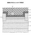
最初に、ゲート電極と半導体層との間に絶縁膜を形成した構造のトランジスタにおいて、保護膜として絶縁膜を形成した構造のトランジスタについて説明する。図1に示されるように、この構造のトランジスタは、HEMT(High Electron Mobility Transistor)と呼ばれるものであり、半導体等からなる基板11上に、電子走行層12、障壁層13、キャップ層14がエピタキシャル成長により積層して形成されている。また、障壁層13と接続されるソース電極15及びドレイン電極16が形成されており、キャップ層14上には、絶縁膜17が形成されており、絶縁膜17上にはゲート電極18が形成されている。更に、絶縁膜17を含む領域の全体を覆うように保護膜19が形成されている。[First Embodiment]
First, a transistor having an insulating film formed between a gate electrode and a semiconductor layer and having an insulating film as a protective film will be described. As shown in FIG. 1, the transistor having this structure is called a HEMT (High Electron Mobility Transistor), and an
基板11はSiC基板、サファイア(Al2O3)基板等が用いられており、電子走行層12はi−GaNにより形成されており、障壁層13はn−AlGaNにより形成されており、キャップ層14はn−GaNにより形成されている。また、ソース電極15、ドレイン電極16及びゲート電極18は金属材料により形成されており、絶縁膜17は、プラズマALD(Atomic Layer Deposition)により酸化アルミニウム(Al2O3)膜を成膜することにより形成されている。また、保護膜19は、窒化シリコン(SiN)、酸化シリコン(SiO2)、酸化アルミニウム等により形成される。保護膜19を形成する際には、スループットの向上等の観点より、一般的には、成膜レートが速いプラズマCVD(Chemical Vapor Deposition)が多く用いられている。The
図2には、このように保護膜の形成されたトランジスタにおけるゲート−ソース電圧(Vgs)とゲート−ソース電流(Igs)との関係及びゲート−ドレイン電圧(Vgd)とゲート−ドレイン電流(Igd)との関係を示す。また、図3には、保護膜19が成膜される前の状態のトランジスタにおけるゲート−ソース電圧(Vgs)とゲート−ソース電流(Igs)との関係及びゲート−ドレイン電圧(Vgd)とゲート−ドレイン電流(Igd)との関係を示す。 FIG. 2 shows the relationship between the gate-source voltage (Vgs) and the gate-source current (Igs) and the gate-drain voltage (Vgd) and the gate-drain current (Igd) in the transistor having the protective film formed as described above. Shows the relationship. FIG. 3 shows the relationship between the gate-source voltage (Vgs) and the gate-source current (Igs) and the gate-drain voltage (Vgs) and the gate− in the transistor before the
図2及び図3に示されるように、保護膜19を成膜する前の状態では、ゲート−ソース電流(Igs)及びゲート−ドレイン電流(Igd)は、約10nA/mm以下と低い値を示しているのに対し、保護膜19を成膜することによりともに大幅に増加している。即ち、保護膜19を形成した構造のトランジスタは、保護膜19が形成されていない構造のトランジスタと比較して、ゲートリーク電流が大幅に増加している。言い換えるならば、保護膜19を形成することにより、トランジスタのゲートリーク電流が増加し、特性が低下してしまうのである。尚、同様の傾向は、絶縁膜17にHfO2を用いた場合においても確認されている。As shown in FIGS. 2 and 3, the gate-source current (Igs) and the gate-drain current (Igd) are as low as about 10 nA / mm or less before the
発明者らは、このように保護膜19を形成することによりゲートリーク電流が大幅に増加してしまうことについて検討を行なったところ、保護膜19の成膜方法に原因があることを見出した。 The inventors have studied that the gate leakage current is greatly increased by forming the

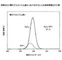
表1は、保護膜19となる酸化アルミニウム膜の成膜方法と、ソース−ドレイン間における絶縁耐圧との関係を示すものである。表1に示されるように、保護膜19が形成されていない状態において絶縁耐圧が390Vであるトランジスタに、保護膜19として酸化アルミニウム膜をプラズマCVDにより成膜した場合、絶縁耐圧は150Vと大幅に低下した。また、保護膜19が形成されていない状態において絶縁耐圧が400Vであるトランジスタに、保護膜19として酸化アルミニウム膜をプラズマCVDにより成膜した場合、絶縁耐圧は200Vに低下した。また、保護膜19が形成されていない状態において絶縁耐圧が380Vであるトランジスタに、保護膜19として酸化アルミニウム膜をスパッタリングにより成膜した場合、絶縁耐圧は140Vに低下した。一方、保護膜19が形成されていない状態において絶縁耐圧が400Vであるトランジスタに、保護膜19として酸化アルミニウム膜を熱ALDにより成膜した場合、絶縁耐圧は変化することなく400Vであった。尚、熱ALDとは、プラズマを発生させることなく、加熱された基板に、成膜のための原料となるガスを交互に供給することにより成膜を行なう方法である。 Table 1 shows the relationship between the method for forming the aluminum oxide film serving as the
上記に基づくならば、前述したように保護膜19を成膜したトランジスタにおいて、ゲートリーク電流が増加する原因は、保護膜19となる酸化アルミニウム膜をプラズマCVDにより成膜することに起因するものと推察される。 Based on the above, the reason why the gate leakage current increases in the transistor having the
また、プラズマCVD、プラズマALD及びスパッタリングは、成膜の際にプラズマを用いるプラズマプロセスであるのに対し、熱ALDは、成膜の際にプラズマを用いないプロセスであるという特徴がある。 In addition, plasma CVD, plasma ALD, and sputtering are plasma processes that use plasma at the time of film formation, whereas thermal ALD is a process that does not use plasma at the time of film formation.
従って、プラズマプロセスにより保護膜19となる酸化アルミニウム膜を成膜することにより、絶縁耐圧が低下し、トランジスタのゲートリーク電流が増加するものと考えられる。このため、保護膜19となる酸化アルミニウム膜を熱ALDにより成膜した場合には、絶縁耐圧が低下しない。従って、保護膜19となる酸化アルミニウム膜を熱ALD等のプラズマを用いない成膜プロセスにより成膜することにより、ゲートリーク電流の増加を防ぐことができるものと考えられる。ここで、プラズマを用いない保護膜の成膜方法としては、熱ALD、熱CVD、真空蒸着(抵抗加熱、EB(Electron Beam)蒸着の双方を含む)等が挙げられる。 Therefore, it is considered that by forming an aluminum oxide film serving as the
次に、プラズマCVD等のプラズマプロセスにより保護膜19となる酸化アルミニウム膜を成膜した場合において、ゲートリーク電流が増加するメカニズムについて説明する。図4は、絶縁膜17及びゲート電極18が形成されているものの上に、プラズマを用いた成膜方法により保護膜19を成膜している状態を示すものである。このように、プラズマを用いた成膜方法においては、プラズマ30を発生させることにより生じた荷電粒子が、ゲート電極18から絶縁膜17に侵入し、この荷電粒子によって絶縁膜17内に欠陥が発生し、ゲートリーク電流が増加することが考えられる。また、露出している絶縁膜17がプラズマに曝されるため、絶縁膜17の表面部分において、プラズマダメージによる欠陥等が生じ、ゲートリーク電流が増加することも考えられる。このような観点から考えるならば、絶縁膜17に金属酸化物、酸窒化物、窒化物を用いた場合においても同様に、プラズマCVD等のプラズマプロセスにより保護膜19を成膜することにより耐圧が低下するものと考えられる。 Next, the mechanism by which the gate leakage current increases when an aluminum oxide film serving as the
ところで、このように保護膜19をプラズマCVD等のプラズマプロセスにより成膜した場合のトランジスタにおける耐圧の低下は、従来から生じていたものと考えられる。しかしながら、このことが従来問題にならなかったのは、従来トランジスタに用いていた半導体材料が、Si、GaAs等であり、GaN等と比べてバンドギャップが狭い材料であることによるものと考えられる。即ち、上述した耐圧の低下が問題となる電圧の範囲に対し、実際に使用される電圧の範囲が低いため、保護膜19をプラズマCVD等のプラズマプロセスにより成膜したことに起因する耐圧の低下が、実用上問題になることはなかったものと考えられる。言い換えるならば、半導体材料として、バンドギャップの広いGaNを用いることにより、プラズマCVD等のプラズマプロセスにより保護膜19を形成した場合に生じていた耐圧の低下の問題が顕在化したものと考えられる。 By the way, it is considered that the reduction in the breakdown voltage in the transistor when the
尚、プラズマALDにより酸化アルミニウム膜を成膜する方法としては、原料として、TMA(トリメチルアルミニウム:(CH3)3Al)と、酸素を供給しプラズマを発生させることにより行なわれる。また、プラズマALDにより酸化アルミニウム膜を成膜する方法としては、原料として、TMAと、酸素プラズマとを交互に供給することにより行なわれる。また、スパッタリングにより酸化アルミニウム膜を成膜する方法としては、ターゲットとして酸化アルミニウムを用いスパッタガスとしてArと酸素を用いてスパッタリングを行なう方法、または、ターゲットとしてAlを用いスパッタガスとしてArと酸素を用いてスパッタリングを行なう方法により行なわれる。更に、熱ALDにより酸化アルミニウム膜を成膜する方法としては、基板を加熱した状態において、原料として、TMAと、水とを交互に供給することにより行なわれる。よって、熱ALDにおいては、成膜チャンバー内においてプラズマが発生されることはない。A method for forming an aluminum oxide film by plasma ALD is performed by supplying TMA (trimethylaluminum: (CH3 )3 Al) and oxygen as raw materials to generate plasma. As a method for forming an aluminum oxide film by plasma ALD, TMA and oxygen plasma are alternately supplied as raw materials. As a method for forming an aluminum oxide film by sputtering, sputtering is performed using aluminum oxide as a target and Ar and oxygen as sputtering gases, or using Al as a target and Ar and oxygen as sputtering gases. The method is performed by sputtering. Further, as a method of forming an aluminum oxide film by thermal ALD, TMA and water are alternately supplied as raw materials while the substrate is heated. Therefore, in thermal ALD, plasma is not generated in the deposition chamber.
ところで、プラズマCVDにより成膜された絶縁膜には、成膜された絶縁膜中には水素分子が5×10²⁰個/cm3以上含まれている。また、プラズマALDにより成膜された絶縁膜には、成膜された絶縁膜中に含まれる水素分子が1×1020個/cm3以下であり、水分子が1×1020個/cm3以下である。また、熱ALDにより成膜された絶縁膜には、成膜された絶縁膜中に含まれる水素分子が1×1020個/cm3以下であり、水分子が1×1020個/cm3以上である。このように、絶縁膜中における水素分子の量及び水分子の量を測定することにより、成膜方法を特定することが可能である。By the way, the insulating film formed by plasma CVD includes 5 × 10²⁰ hydrogen molecules / cm3 or more in the formed insulating film. In the insulating film formed by plasma ALD, the number of hydrogen molecules contained in the formed insulating film is 1 × 10²⁰ pieces / cm3 or less, and the number of water molecules is 1 × 10²⁰ pieces / cm3. It is as follows. Also, the insulating film formed by thermal ALD is hydrogen molecules contained in the formed insulating film is at 1 ×10 20 / cm3 or less, water molecules are 1 ×10 20 / cm3 That's it. In this manner, the film formation method can be specified by measuring the amount of hydrogen molecules and the amount of water molecules in the insulating film.
(半導体装置の製造方法)
次に、本実施の形態における半導体装置の製造方法について図5から図7に基づき説明する。(Method for manufacturing semiconductor device)
Next, a method for manufacturing a semiconductor device in the present embodiment will be described with reference to FIGS.
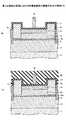
最初に、図5(a)に示されるように、基板11上に、不図示の核形成層を形成し、電子走行層12、障壁層13、キャップ層14等の半導体層をMOVPE(Metal-Organic Vapor Phase Epitaxy)等によりエピタキシャル成長させることにより形成する。 First, as shown in FIG. 5A, a nucleation layer (not shown) is formed on a
基板11は、SiC、サファイア(Al2O3)等の基板が用いられており、基板11上に形成される不図示の核形成層は、例えば、厚さ0.1μmのノンドープのi−AlNにより形成されている。第1の半導体層である電子走行層12は、厚さ3.0μmのノンドープのi−GaNにより形成されており、第2の半導体層である障壁層13は、厚さ20nmノンドープのi−Al0.25Ga0.75Nにより形成されている。また、第3の半導体層であるキャップ層14は、厚さ5nmのn−GaNにより形成されている。尚、上記構造により、電子走行層12において障壁層13に近い側に2次元電子ガス(2DEG:2 dimensional electron gas)が形成される。The
これらの半導体層をMOVPEにより形成する際には、原料ガスとしてTMA(トリメチルアルミニウム)、TMG(トリメチルガリウム)、アンモニア(NH3)等を用い、形成される半導体層の組成に応じて、これらのガスの供給量を調節することにより形成する。尚、これらの半導体層を形成する際に流されるアンモニアの流量は、100ccm〜10LMであり、これら半導体層を結晶成長させる際のチャンバー内の圧力は、50〜300Torrであり、成長温度は1000〜1200℃である。また、障壁層13は、Al0.25Ga0.75Nにn型となる不純物をドープしたものであってもよい。また、半導体層は、MOVPEの他、MBE(Molecular Beam Epitaxy)により半導体層を結晶成長させることにより形成してもよい。また、障壁層13は、AlGaN以外にも、InGaN、InAlN、InAlGaN等により形成することも可能である。When these semiconductor layers are formed by MOVPE, TMA (trimethylaluminum), TMG (trimethylgallium), ammonia (NH3 ), or the like is used as a source gas, and depending on the composition of the semiconductor layer to be formed, It is formed by adjusting the gas supply amount. The flow rate of ammonia that flows when forming these semiconductor layers is 100 ccm to 10 LM, the pressure in the chamber for crystal growth of these semiconductor layers is 50 to 300 Torr, and the growth temperature is 1000 to 1200 ° C. Further, the
次に、図5(b)に示されるように、素子分離領域21を形成する。具体的には、キャップ層14の表面にフォトレジストを塗布し、露光装置による露光、現像を行なうことにより素子分離領域21が形成される領域に開口部を有するレジストパターンを形成する。この後、形成されたレジストパターンをマスクとして、電子走行層13まで達するように不純物イオンのイオン注入を行なうことにより、素子分離領域21を形成する。尚、レジストパターンは、この後除去する。また、別の素子分離領域21の形成方法としては、レジストパターンをマスクとしてドライエッチング等によりレジストパターンが形成されていない領域におけるキャップ層14、障壁層13及び電子走行層12の一部を除去することにより形成してもよい。この後、必要に応じて半導体層の除去された領域に酸化膜を埋め込み形成する。 Next, as shown in FIG. 5B, an
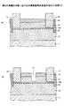
次に、図6(a)に示されるように、ソース電極15及びドレイン電極16を形成する。具体的には、キャップ層14上にフォトレジストを塗布し、露光装置による露光、現像を行なうことにより、ソース電極15及びドレイン電極16が形成される領域に開口部を有するレジストパターンを形成する。この後、塩素ガスを用いたRIE等によるドライエッチングによりレジストパターンの形成されていない領域のキャップ層14及び障壁層13の一部を除去する。この際行なわれるドライエッチングは、チャンバー内にエッチングガスとして塩素ガスを約30sccmを導入し、チャンバー内の圧力を約2Paに設定し、RFパワーを20W印加することにより行なわれる。この後、真空蒸着等によりTa/Alの積層膜等からなる金属膜を成膜した後、リフトオフによりレジストパターンの形成されている領域の金属膜をレジストパターンとともに除去することによりソース電極15及びドレイン電極16を形成する。尚、リフトオフを行なった後580℃の熱処理を行なうことによりオーミックコンタクトさせる。 Next, as shown in FIG. 6A, the
次に、図6(b)に示されるように、キャップ層14、ソース電極15及びドレイン電極16上に、絶縁膜17を形成する。絶縁膜17としては、シリコン、アルミニウム、ハフニウム、タンタル、ジルコニウム、イットリウム、ランタン、タンタルの酸化物、シリコン、アルミニウムの窒化物、または、シリコンの酸窒化物のうち、いずれか1または2以上の材料を含むものである。尚、形成される絶縁膜17としては、比誘電率が高い材料が好ましく、また、実用上の観点からは、SiO2、SiN、Al2O3、SiON、HfO2がより好ましい。形成される絶縁膜17の膜厚は、2nm〜200nmであり、成膜方法としては、プラズマALD、プラズマCVD、スパッタリングにより成膜される。例えば、プラズマCVDにより酸化アルミニウムからなる絶縁膜17を形成する場合では、原料ガスとしてトリメチルアルミニウム(TMA)と酸素を供給し、プラズマを発生させることにより成膜する。Next, as illustrated in FIG. 6B, an insulating
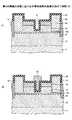
次に、図7(a)に示されるように、ゲート電極18を形成する。具体的には、絶縁膜17上に、フォトレジストを塗布し、露光装置による露光、現像を行なうことにより、ゲート電極18の形成される領域に開口部を有するレジストパターンを形成する。この後、真空蒸着等によりNi/Auからなる積層膜等からなる金属膜を成膜した後、リフトオフによりレジストパターンの形成されている領域の金属膜をレジストパターンとともに除去することによりゲート電極18を形成する。 Next, as shown in FIG. 7A, the
次に、図7(b)に示されるように、保護膜20を形成する。保護膜20は、シリコン、アルミニウム、ハフニウム、タンタル、ジルコニウム、イットリウム、ランタン、タンタルの酸化物、シリコン、アルミニウムの窒化物、または、シリコンの酸窒化物のうち、いずれか1または2以上の材料を含むものである。保護膜20は、成膜の際にプラズマを用いない成膜方法により形成される。例えば、熱ALD、熱CVD、真空蒸着等の方法により形成される。尚、酸化アルミニウムからなる保護膜20を熱ALDにより形成する場合においては、基板を200℃〜400℃に加熱した状態で、トリメチルアルミニウムと水を交互に供給することにより形成する。 Next, as shown in FIG. 7B, a
これにより、本実施の形態における半導体装置を製造することができる。本実施の形態における半導体装置では、保護膜20がプラズマを発生させない成膜方法により成膜しているため、保護膜20が形成されたトランジスタにおいても耐圧が低下することがない。 Thereby, the semiconductor device in the present embodiment can be manufactured. In the semiconductor device in this embodiment, since the
〔第2の実施の形態〕
次に、第2の実施の形態について説明する。本実施の形態における半導体装置の製造方法について、図8から図10に基づき説明する。[Second Embodiment]
Next, a second embodiment will be described. A method for manufacturing a semiconductor device in the present embodiment will be described with reference to FIGS.
最初に、図8(a)に示されるように、基板11上に、不図示の核形成層を形成し、電子走行層12、障壁層13、キャップ層14等の半導体層をMOVPE(Metal-Organic Vapor Phase Epitaxy)等によりエピタキシャル成長させることにより形成する。 First, as shown in FIG. 8A, a nucleation layer (not shown) is formed on a
基板11は、SiC、サファイア(Al2O3)等の基板が用いられており、基板11上に形成される不図示の核形成層は、例えば、厚さ0.1μmのノンドープのi−AlNにより形成されている。電子走行層12は、厚さ3.0μmのノンドープのi−GaNにより形成されており、障壁層13は、厚さ20nmノンドープのi−Al0.25Ga0.75Nにより形成されている。また、キャップ層14は、厚さ5nmのn−GaNにより形成されている。The
次に、図8(b)に示されるように、素子分離領域21を形成する。具体的には、キャップ層14の表面にフォトレジストを塗布し、露光装置による露光、現像を行なうことにより素子分離領域21が形成される領域に開口部を有するレジストパターンを形成する。この後、形成されたレジストパターンをマスクとして、電子走行層13まで達するように不純物イオンのイオン注入を行なうことにより、素子分離領域21を形成する。 Next, as shown in FIG. 8B, an
次に、図9(a)に示されるように、ソース電極15及びドレイン電極16を形成する。具体的には、キャップ層14上にフォトレジストを塗布し、露光装置による露光、現像を行なうことにより、ソース電極15及びドレイン電極16が形成される領域に開口部を有するレジストパターンを形成する。この後、塩素ガスを用いたRIE等によるドライエッチングによりレジストパターンの形成されていない領域のキャップ層14及び障壁層13の一部を除去する。この後、真空蒸着等によりTa/Alの積層膜等からなる金属膜を成膜した後、リフトオフによりレジストパターンの形成されている領域の金属膜をレジストパターンとともに除去することによりソース電極15及びドレイン電極16を形成する。尚、リフトオフを行なった後580℃の熱処理を行なうことによりオーミックコンタクトさせる。 Next, as shown in FIG. 9A, the
次に、図9(b)に示されるように、リセス開口部31を形成する。具体的には、キャップ層14上にフォトレジストを塗布し、露光装置による露光、現像を行なうことにより、リセス開口部31の形成される領域に開口を有するレジストパターンを形成する。この後、レジストパターンをマスクとして、塩素を含むガスを導入してRIE等によるドライエッチングにより、レジストパターンの形成されていない領域のキャップ層14及び障壁層13の一部を除去する。この後、レジストパターンは除去される。尚、本実施の形態では、上述したRIE等によるドライエッチングの際には、酸素またはフッ素を混合してもよい。また、リセス開口部31は、キャップ層14の一部を除去することによりに形成した構造のもの、また、キャップ層14、障壁層13、電子走行層12の一部を除去することにより形成した構造のものであってもよい。 Next, as shown in FIG. 9B, a
次に、図10(a)に示されるように、リセス開口部31の表面、キャップ層14、ソース電極15及びドレイン電極16上に、絶縁膜32を形成する。絶縁膜32は、シリコン、アルミニウム、ハフニウム、タンタル、ジルコニウム、イットリウム、ランタン、タンタルの酸化物、シリコン、アルミニウムの窒化物、または、シリコンの酸窒化物のうち、いずれか1または2以上の材料を含むもの等である。 Next, as illustrated in FIG. 10A, an insulating
尚、形成される絶縁膜17としては、比誘電率が高い材料が好ましく、また、実用上の観点からは、SiO2、SiN、Al2O3、SiON、HfO2がより好ましい。形成される絶縁膜17の膜厚は、2nm〜200nmであり、成膜方法としては、プラズマALD、プラズマCVD、スパッタリングにより成膜される。例えば、プラズマCVDにより酸化アルミニウムからなる絶縁膜32を形成する場合では、原料ガスとしてトリメチルアルミニウム(TMA)と酸素を供給し、プラズマを発生させることにより成膜する。As the insulating
次に、図10(b)に示されるように、ゲート電極33を形成する。具体的には、絶縁膜32上に、フォトレジストを塗布し、露光装置による露光、現像を行なうことにより、リセス開口部31を含む領域に開口を有するレジストパターンを形成する。この後、真空蒸着等によりNi/Auからなる積層膜等からなる金属膜を成膜した後、リフトオフによりレジストパターンの形成されている領域の金属膜をレジストパターンとともに除去することによりゲート電極33を形成する。 Next, as shown in FIG. 10B, the
次に、図11に示されるように、保護膜34を形成する。保護膜34は絶縁体材料からなる膜であって、例えば、酸化アルミニウムが好ましい。保護膜34は、成膜の際にプラズマを用いない成膜方法により形成される。例えば、熱ALD、熱CVD、真空蒸着等の方法により形成される。尚、酸化アルミニウムからなる保護膜34を熱ALDにより形成する場合においては、基板温度を200℃〜400℃に加熱した状態で、TMAと水を交互に供給することにより形成する。 Next, as shown in FIG. 11, a
これにより、本実施の形態における半導体装置を製造することができる。 Thereby, the semiconductor device in the present embodiment can be manufactured.
尚、上記以外の内容については、第1の実施の形態と同様である。 The contents other than the above are the same as in the first embodiment.
〔第3の実施の形態〕
次に、第3の実施の形態について説明する。ところで、絶縁膜上に保護膜を形成することにより、耐圧が低下する理由としては、絶縁膜と保護膜との熱膨張率の差に起因する場合や、保護膜の成膜の際に生じる応力に起因する場合や、絶縁膜と保護膜との間等に水分が残留することに起因する場合が考えられる。[Third Embodiment]
Next, a third embodiment will be described. By the way, the reason why the breakdown voltage is lowered by forming a protective film on the insulating film is that the stress caused by the difference in thermal expansion coefficient between the insulating film and the protective film or the stress generated during the formation of the protective film. It is conceivable that this is caused by water or if moisture remains between the insulating film and the protective film.
このような観点に基づくならば、絶縁膜と保護膜とをともに金属酸化膜により形成することにより、絶縁膜と保護膜との熱膨張係数の差を2ppm以下に低減することが可能である。更には、絶縁膜と保護膜をともに同じ材料により形成することにより、絶縁膜と保護膜との差を略0にすることができる。この際用いられる金属酸化膜としては、アルミニウム、ハフニウム、ジルコニウム、イットリウム、ランタン、タンタルのうち、1または2以上の元素を含む金属酸化膜が挙げられる。また、耐圧を高めるため、絶縁膜と保護膜は、アモルファス状態であることが好ましい。 Based on such a viewpoint, it is possible to reduce the difference in thermal expansion coefficient between the insulating film and the protective film to 2 ppm or less by forming both the insulating film and the protective film from the metal oxide film. Furthermore, the difference between the insulating film and the protective film can be made substantially zero by forming both the insulating film and the protective film from the same material. Examples of the metal oxide film used at this time include metal oxide films containing one or more elements of aluminum, hafnium, zirconium, yttrium, lanthanum, and tantalum. In order to increase the withstand voltage, the insulating film and the protective film are preferably in an amorphous state.
次に、本実施の形態における半導体装置の製造方法について説明する。本実施の形態における半導体装置の製造方法は、第2の実施の形態における半導体装置の製造方法において保護膜34の成膜方法が異なるものである。図12に基づき保護膜34の成膜方法について説明する。 Next, a method for manufacturing a semiconductor device in the present embodiment will be described. The manufacturing method of the semiconductor device in the present embodiment is different from the manufacturing method of the semiconductor device in the second embodiment in the method of forming the
最初に、ステップ102(S102)に示すように、熱ALDまたは熱CVDにより、酸化アルミニウムからなる膜を50nm成膜する。成膜される酸化アルミニウムからなる膜の膜厚は、10nm以上、50nm以下であることが好ましい。成膜される酸化アルミニウムからなる膜の膜厚が10nm以下では、生産性の観点から実用性に乏しいからである。また、50nmを超える膜厚で成膜した場合、後述する熱処理の際に穴が発生してしまう。この穴は、脱離水分の影響により発生するものと考えられ、膜厚が厚くなるほど発生頻度が高くなり、また、経験上、膜厚が50nm以下であれば、穴が発生し難いという知見が得られている。よって、一回に形成される酸化アルミニウムからなる膜の膜厚は50nm以下であることが好ましい。 First, as shown in step 102 (S102), a film made of aluminum oxide is formed to a thickness of 50 nm by thermal ALD or thermal CVD. The film thickness of the film made of aluminum oxide is preferably 10 nm or more and 50 nm or less. This is because when the film thickness of the film made of aluminum oxide is 10 nm or less, the practicality is poor from the viewpoint of productivity. Moreover, when it forms into a film thickness exceeding 50 nm, a hole will generate | occur | produce in the heat processing mentioned later. This hole is considered to be generated due to the influence of desorbed moisture, and the frequency of occurrence increases as the film thickness increases, and experience has shown that if the film thickness is 50 nm or less, it is difficult to generate holes. Has been obtained. Therefore, the film thickness of the aluminum oxide film formed at a time is preferably 50 nm or less.
次に、ステップ104(S104)に示すように、700℃で熱処理を行なう。熱処理温度は、後述する脱離水分の結果に基づき、500℃以上、800℃以下が好ましく、650℃以上、800℃以下がより好ましい。熱処理温度が800℃を超える場合、アモルファス状態から結晶化状態に変化する可能性があるため、熱処理の温度は800℃以下であることが好ましい。 Next, as shown in step 104 (S104), heat treatment is performed at 700 ° C. The heat treatment temperature is preferably 500 ° C. or higher and 800 ° C. or lower, more preferably 650 ° C. or higher and 800 ° C. or lower, based on the result of desorbed moisture described later. When the heat treatment temperature exceeds 800 ° C., the heat treatment temperature is preferably 800 ° C. or lower because there is a possibility of changing from an amorphous state to a crystallized state.
次に、ステップ106(S106)に示すように、成膜された酸化アルミニウム膜が保護膜34として所定の膜厚となっているか否かが判断される。成膜された酸化アルミニウム膜が所定の膜厚になっているものと判断された場合には、保護膜34の成膜は終了する。一方、成膜された酸化アルミニウム膜が所定の膜厚に満たないものと判断された場合には、ステップ102に移行し、所定の膜厚になるまで酸化アルミニウムからなる膜の成膜と熱処理が繰り返される。 Next, as shown in step 106 (S106), it is determined whether or not the formed aluminum oxide film has a predetermined thickness as the
このような方法により、保護膜34を形成することにより、金属酸化膜の多層膜からな保護膜34を形成することができる。 By forming the
次に、形成された保護膜34となる酸化アルミニウム膜のX線光電子分光(XPS:X-ray photoelectron spectroscopy)法による分析結果について説明する。尚、測定装置としては、AXIS−Hsi(島津製作所(株)製)を用いた。 Next, the analysis result by the X-ray photoelectron spectroscopy (XPS) method of the aluminum oxide film used as the
図13には、熱CVDにより酸化アルミニウム膜を連続して成膜した場合を示し、図14には、図12に示される本実施の形態における保護膜の成膜方法により酸化アルミニウム膜を成膜した場合を示す。尚、酸化アルミニウム膜を成膜するための基板にはシリコン基板を用い、双方とも約200nmの酸化アルミニウム膜を成膜し測定を行なった。熱CVDにより連続して成膜された酸化アルミニウム膜Bでは、水酸基(AlOH)が32%含まれているのに対し、本実施の形態における保護膜の成膜方法により成膜された酸化アルミニウム膜Aでは、水酸基(AlOH)は18%含まれるものであった。このように本実施の形態における保護膜の成膜方法により酸化アルミニウム膜を成膜した場合では、大幅に含有する水酸基を低減させることができる。尚、金属酸化膜中に水酸基(−OH)が含まれると、水素結合により水分が吸着しやすくなるとともに、成膜プロセス等における熱履歴により水酸基同士が脱水縮合して水分が脱離してしまう。従って、酸化アルミニウム膜に含まれる水酸基は少ない方が好ましい。 FIG. 13 shows a case where an aluminum oxide film is continuously formed by thermal CVD, and FIG. 14 shows an aluminum oxide film formed by the method for forming a protective film in the present embodiment shown in FIG. Shows the case. A silicon substrate was used as the substrate for forming the aluminum oxide film, and both were measured by forming an aluminum oxide film of about 200 nm. The aluminum oxide film B continuously formed by thermal CVD contains 32% of hydroxyl groups (AlOH), whereas the aluminum oxide film formed by the method for forming a protective film in the present embodiment In A, 18% of the hydroxyl group (AlOH) was contained. As described above, in the case where the aluminum oxide film is formed by the method for forming the protective film in this embodiment, the hydroxyl groups contained can be significantly reduced. Note that when a hydroxyl group (—OH) is contained in the metal oxide film, moisture is easily adsorbed by hydrogen bonds, and the hydroxyl groups are dehydrated and condensed due to thermal history in a film forming process or the like, and moisture is desorbed. Therefore, it is preferable that the number of hydroxyl groups contained in the aluminum oxide film is small.
次に、成膜された酸化アルミニウム膜について、加熱昇温脱ガス装置(EMD1000、電子化学(株)製)を用い、TDS(Thermal Desorption Spectroscopy)法により測定した結果を図15に示す。図15に示されるように、熱CVDにより酸化アルミニウム膜を連続して成膜した酸化アルミニウム膜Bでは、550℃以上加熱することにより、水酸基同士の脱水縮合による脱離水分が検出された。これに対し、本実施の形態における保護膜の成膜方法により酸化アルミニウム膜を成膜した酸化アルミニウム膜Aでは、脱離水分は殆ど検出されなかった。尚、酸化アルミニウム膜Bでは、500℃以上の温度で脱離水分が検出され始め、650℃では、検出される脱離水分の値が最大となる。よって、熱処理温度は、500℃以上、800℃以下が好ましく、650℃以上、800℃以下がより好ましい。 Next, FIG. 15 shows the result of measuring the formed aluminum oxide film by a TDS (Thermal Desorption Spectroscopy) method using a heating temperature rising degassing apparatus (EMD1000, manufactured by Denki Kagaku Co., Ltd.). As shown in FIG. 15, in the aluminum oxide film B in which aluminum oxide films were continuously formed by thermal CVD, desorption moisture due to dehydration condensation between hydroxyl groups was detected by heating at 550 ° C. or more. On the other hand, almost no desorbed moisture was detected in the aluminum oxide film A in which the aluminum oxide film was formed by the protective film forming method in the present embodiment. In the aluminum oxide film B, the desorbed moisture starts to be detected at a temperature of 500 ° C. or higher, and the detected desorbed water value becomes maximum at 650 ° C. Therefore, the heat treatment temperature is preferably 500 ° C. or higher and 800 ° C. or lower, and more preferably 650 ° C. or higher and 800 ° C. or lower.
次に、成膜された保護膜について、絶縁耐圧試験を行なった結果を図16に示す。絶縁耐圧試験は、図17に示される試料を作製して行なった。この試料は、基板110上に酸化アルミニウム膜111を成膜し、酸化アルミニウム膜111上に電極112及び113を形成し、更に、電極112と電極113との間の酸化アルミニウム膜111上に測定の対象となる保護膜112を形成した構造のものである。このような試料の電極112及び113にI−Vメータ115に接続し試験を行なった。絶縁膜114としては、SiN膜、熱CVDにより連続して成膜した酸化アルミニウム膜B、本実施の形態における保護膜の成膜方法により成膜した酸化アルミニウム膜Aの各々が形成された試料を各々作製し測定を行なった。この結果、本実施の形態における保護膜の成膜方法により形成された酸化アルミニウム膜Aの試料が最も絶縁耐圧が高く、絶縁膜114が成膜されていないもの(酸化アルミニウム膜111と電極112及び113が形成されているもの)の耐圧と略等しい値であった。 Next, FIG. 16 shows the result of the dielectric strength test performed on the formed protective film. The dielectric strength test was performed by preparing the sample shown in FIG. In this sample, an aluminum oxide film 111 is formed on a
尚、本実施の形態は、第1の実施の形態における半導体装置にも適用可能である、また、上記以外の内容については、第1の実施の形態、または、第2の実施の形態と同様である。 This embodiment can also be applied to the semiconductor device according to the first embodiment, and the contents other than the above are the same as those of the first embodiment or the second embodiment. It is.
以上、実施の形態について詳述したが、特定の実施形態に限定されるものではなく、特許請求の範囲に記載された範囲内において、種々の変形及び変更が可能である。 Although the embodiment has been described in detail above, it is not limited to the specific embodiment, and various modifications and changes can be made within the scope described in the claims.
上記の説明に関し、更に以下の付記を開示する。
(付記1)
基板上に形成された第1の半導体層と、
前記第1の半導体層上に形成された第2の半導体層と、
前記第2の半導体層上に形成されたソース電極及びドレイン電極と、
前記第2の半導体層上に形成された絶縁膜と、
前記絶縁膜上に形成されたゲート電極と、
前記絶縁膜を覆うように形成された保護膜と、
を有し、
前記保護膜は、熱CVD、熱ALD、真空蒸着のいずれかにより形成されたものであることを特徴とする半導体装置。
(付記2)
基板上に形成された第1の半導体層と、
前記第1の半導体層上に形成された第2の半導体層と、
前記第2の半導体層上に形成されたソース電極及びドレイン電極と、
前記第2の半導体層または、前記第2の半導体層及び前記第1の半導体層に形成されたリセス開口部と、
前記第2の半導体層上及び前記リセス開口部内に形成された絶縁膜と、
前記リセス開口部内の前記絶縁膜上に形成されたゲート電極と、
前記絶縁膜を覆うように形成された保護膜と、
を有し、
前記保護膜は、熱CVD、熱ALD、真空蒸着のいずれかにより形成されたものであることを特徴とする半導体装置。
(付記3)
前記保護膜は、金属酸化膜であることを特徴とする付記1または2に記載の半導体装置。
(付記4)
前記保護膜は、シリコン、アルミニウム、ハフニウム、タンタル、ジルコニウム、イットリウム、ランタン、タンタルの酸化物、シリコン、アルミニウムの窒化物、または、シリコンの酸窒化物のうち、いずれか1または2以上の材料を含むものであることを特徴とする付記1から3のいずれか1項に記載の半導体装置。
(付記5)
前記保護膜は、多層膜により形成されていることを特徴とする付記1から4のいずれか1項に記載の半導体装置。
(付記6)
前記絶縁膜は金属酸化膜であることを特徴とする付記1から5のいずれか1項に記載の半導体装置。
(付記7)
前記絶縁膜は、シリコン、アルミニウム、ハフニウム、タンタル、ジルコニウム、イットリウム、ランタン、タンタルの酸化物、シリコン、アルミニウムの窒化物、または、シリコンの酸窒化物のうち、いずれか1または2以上の材料を含むものであることを特徴とする付記1から5のいずれか1項に記載の半導体装置。
(付記8)
前記絶縁膜は、プラズマCVD、プラズマALDまたはスパッタリングにより形成されたものであることを特徴とする付記1から7のいずれか1項に記載の半導体装置。
(付記9)
前記保護膜と前記絶縁膜は、同じ材料を含むものであることを特徴とする付記1から8のいずれか1項に記載の半導体装置。
(付記10)
前記第2の半導体層と前記絶縁膜との間には、第3の半導体層が設けられていることを特徴とする付記1から9のいずれか1項に記載の半導体装置。
(付記11)
基板上に第1の半導体層と、第2の半導体層を積層形成する工程と、
前記第2の半導体層上にソース電極及びドレイン電極を形成する工程と、
前記第2の半導体層上に絶縁膜を形成する工程と、
前記絶縁膜上にゲート電極を形成する工程と、
前記絶縁膜を覆うように熱CVD、熱ALD、真空蒸着のいずれかにより保護膜を形成する工程と、
を有することを特徴とする半導体装置の製造方法。
(付記12)
基板上に第1の半導体層と、第2の半導体層を積層形成する工程と、
前記第2の半導体層上にソース電極及びドレイン電極を形成する工程と、
前記第2の半導体層にリセス開口部を形成する工程と、
前記第2の半導体層の上方及び前記リセス開口部内に絶縁膜を形成する工程と、
前記リセス開口部内の前記絶縁膜上にゲート電極を形成する工程と、
前記絶縁膜を覆うように熱CVD、熱ALD、真空蒸着のいずれかにより保護膜を形成する工程と、
を有することを特徴とする半導体装置の製造方法。
(付記13)
前記保護膜を形成する工程は、トリメチルアルミニウムと水とを交互に供給することにより、熱ALDによって酸化アルミニウム膜を形成するものであることを特徴とする付記11または12に記載の半導体装置の製造方法。
(付記14)
前記保護膜を形成する工程は、
10nm以上、50nm以下の膜厚の金属酸化膜を成膜する工程と、
前記金属酸化膜を成膜後、500℃以上、800℃以下の温度で熱処理を行なう工程と、
を繰り返し行なうものであることを特徴とする付記11から13のいずれか1項に記載の半導体装置の製造方法。In addition to the above description, the following additional notes are disclosed.
(Appendix 1)
A first semiconductor layer formed on a substrate;
A second semiconductor layer formed on the first semiconductor layer;
A source electrode and a drain electrode formed on the second semiconductor layer;
An insulating film formed on the second semiconductor layer;
A gate electrode formed on the insulating film;
A protective film formed to cover the insulating film;
Have
The semiconductor device according to claim 1, wherein the protective film is formed by any one of thermal CVD, thermal ALD, and vacuum deposition.
(Appendix 2)
A first semiconductor layer formed on a substrate;
A second semiconductor layer formed on the first semiconductor layer;
A source electrode and a drain electrode formed on the second semiconductor layer;
A recess opening formed in the second semiconductor layer or in the second semiconductor layer and the first semiconductor layer;
An insulating film formed on the second semiconductor layer and in the recess opening;
A gate electrode formed on the insulating film in the recess opening;
A protective film formed to cover the insulating film;
Have
The semiconductor device according to claim 1, wherein the protective film is formed by any one of thermal CVD, thermal ALD, and vacuum deposition.
(Appendix 3)
The semiconductor device according to appendix 1 or 2, wherein the protective film is a metal oxide film.
(Appendix 4)
The protective film is made of any one or more of silicon, aluminum, hafnium, tantalum, zirconium, yttrium, lanthanum, tantalum oxide, silicon, aluminum nitride, or silicon oxynitride. 4. The semiconductor device according to any one of appendices 1 to 3, wherein the semiconductor device is included.
(Appendix 5)
5. The semiconductor device according to any one of appendices 1 to 4, wherein the protective film is formed of a multilayer film.
(Appendix 6)
6. The semiconductor device according to any one of appendices 1 to 5, wherein the insulating film is a metal oxide film.
(Appendix 7)
The insulating film is made of any one or more of silicon, aluminum, hafnium, tantalum, zirconium, yttrium, lanthanum, tantalum oxide, silicon, aluminum nitride, or silicon oxynitride. 6. The semiconductor device according to any one of appendices 1 to 5, wherein the semiconductor device is included.
(Appendix 8)
8. The semiconductor device according to any one of appendices 1 to 7, wherein the insulating film is formed by plasma CVD, plasma ALD, or sputtering.
(Appendix 9)
9. The semiconductor device according to any one of appendices 1 to 8, wherein the protective film and the insulating film contain the same material.
(Appendix 10)
10. The semiconductor device according to any one of appendices 1 to 9, wherein a third semiconductor layer is provided between the second semiconductor layer and the insulating film.
(Appendix 11)
Stacking and forming a first semiconductor layer and a second semiconductor layer on a substrate;
Forming a source electrode and a drain electrode on the second semiconductor layer;
Forming an insulating film on the second semiconductor layer;
Forming a gate electrode on the insulating film;
Forming a protective film by thermal CVD, thermal ALD, or vacuum deposition so as to cover the insulating film;
A method for manufacturing a semiconductor device, comprising:
(Appendix 12)
Stacking and forming a first semiconductor layer and a second semiconductor layer on a substrate;
Forming a source electrode and a drain electrode on the second semiconductor layer;
Forming a recess opening in the second semiconductor layer;
Forming an insulating film above the second semiconductor layer and in the recess opening;
Forming a gate electrode on the insulating film in the recess opening;
Forming a protective film by thermal CVD, thermal ALD, or vacuum deposition so as to cover the insulating film;
A method for manufacturing a semiconductor device, comprising:
(Appendix 13)
13. The manufacturing method of a semiconductor device according to
(Appendix 14)
The step of forming the protective film includes:
Forming a metal oxide film having a thickness of 10 nm or more and 50 nm or less;
A step of performing a heat treatment at a temperature of 500 ° C. or higher and 800 ° C. or lower after forming the metal oxide film;
14. The method of manufacturing a semiconductor device according to any one of
11 基板
12 電子走行層(第1の半導体層)
13 障壁層(第2の半導体層)
14 キャップ層
15 ソース電極
16 ドレイン電極
17 絶縁膜
18 ゲート電極
19 保護膜
20 保護膜11
13 Barrier layer (second semiconductor layer)
14
Claims (7)
Translated fromJapanese前記第1の半導体層上に形成された第2の半導体層と、
前記第2の半導体層上に形成されたソース電極及びドレイン電極と、
前記第2の半導体層上に形成された絶縁膜と、
前記絶縁膜上に形成されたゲート電極と、
前記絶縁膜を覆うように形成された保護膜と、
を有し、
前記保護膜は、トリメチルアルミニウムと水とを交互に供給することにより、熱ALDにより形成された酸化アルミニウム膜を含むものであることを特徴とする半導体装置。A first semiconductor layer formed on a substrate;
A second semiconductor layer formed on the first semiconductor layer;
A source electrode and a drain electrode formed on the second semiconductor layer;
An insulating film formed on the second semiconductor layer;
A gate electrode formed on the insulating film;
A protective film formed to cover the insulating film;
Have
The protective layer, wherein aby supplying trimethyl aluminum and water alternately, is intendedto include more formedof aluminum oxide filmon the thermal AL D.
前記第1の半導体層上に形成された第2の半導体層と、
前記第2の半導体層上に形成されたソース電極及びドレイン電極と、
前記第2の半導体層または、前記第2の半導体層及び前記第1の半導体層に形成されたリセス開口部と、
前記第2の半導体層上及び前記リセス開口部内に形成された絶縁膜と、
前記リセス開口部内の前記絶縁膜上に形成されたゲート電極と、
前記絶縁膜を覆うように形成された保護膜と、
を有し、
前記保護膜は、トリメチルアルミニウムと水とを交互に供給することにより、熱ALDにより形成された酸化アルミニウム膜を含むものであることを特徴とする半導体装置。A first semiconductor layer formed on a substrate;
A second semiconductor layer formed on the first semiconductor layer;
A source electrode and a drain electrode formed on the second semiconductor layer;
A recess opening formed in the second semiconductor layer or in the second semiconductor layer and the first semiconductor layer;
An insulating film formed on the second semiconductor layer and in the recess opening;
A gate electrode formed on the insulating film in the recess opening;
A protective film formed to cover the insulating film;
Have
The protective layer, wherein aby supplying trimethyl aluminum and water alternately, is intendedto include more formedof aluminum oxide filmon the thermal AL D.
前記第2の半導体層上にソース電極及びドレイン電極を形成する工程と、
前記第2の半導体層上に絶縁膜を形成する工程と、
前記絶縁膜上にゲート電極を形成する工程と、
前記絶縁膜を覆うように保護膜を形成する工程と、
を有し、
前記保護膜を形成する工程は、トリメチルアルミニウムと水とを交互に供給することにより、熱ALDによって酸化アルミニウム膜を形成するものであることを特徴とする半導体装置の製造方法。Stacking and forming a first semiconductor layer and a second semiconductor layer on a substrate;
Forming a source electrode and a drain electrode on the second semiconductor layer;
Forming an insulating film on the second semiconductor layer;
Forming a gate electrode on the insulating film;
Forming acoercive Mamorumakuto cover the insulating film,
I have a,
Step, by supplying trimethyl aluminum and water alternately, a method of manufacturing a semiconductor device according to claimder Rukotowhich forms an aluminum oxide film by thermal ALD forming the protective film.
前記第2の半導体層上にソース電極及びドレイン電極を形成する工程と、
前記第2の半導体層にリセス開口部を形成する工程と、
前記第2の半導体層の上方及び前記リセス開口部内に絶縁膜を形成する工程と、
前記リセス開口部内の前記絶縁膜上にゲート電極を形成する工程と、
前記絶縁膜を覆うように保護膜を形成する工程と、
を有し、
前記保護膜を形成する工程は、トリメチルアルミニウムと水とを交互に供給することにより、熱ALDによって酸化アルミニウム膜を形成するものであることを特徴とする半導体装置の製造方法。Stacking and forming a first semiconductor layer and a second semiconductor layer on a substrate;
Forming a source electrode and a drain electrode on the second semiconductor layer;
Forming a recess opening in the second semiconductor layer;
Forming an insulating film above the second semiconductor layer and in the recess opening;
Forming a gate electrode on the insulating film in the recess opening;
Forming acoercive Mamorumakuto cover the insulating film,
I have a,
Step, by supplying trimethyl aluminum and water alternately, a method of manufacturing a semiconductor device according to claimder Rukotowhich forms an aluminum oxide film by thermal ALD forming the protective film.
10nm以上、50nm以下の膜厚の金属酸化膜を成膜する工程と、
前記金属酸化膜を成膜後、500℃以上、800℃以下の温度で熱処理を行なう工程と、
を繰り返し行なうものであることを特徴とする請求項5または6に記載の半導体装置の製造方法。The step of forming the protective film includes:
Forming a metal oxide film having a thickness of 10 nm or more and 50 nm or less;
A step of performing a heat treatment at a temperature of 500 ° C. or higher and 800 ° C. or lower after forming the metal oxide film;
7. The method of manufacturing a semiconductor device according to claim5 , wherein the step is repeatedly performed.
Priority Applications (5)
| Application Number | Priority Date | Filing Date | Title |
|---|---|---|---|
| JP2010234961AJP5636867B2 (en) | 2010-10-19 | 2010-10-19 | Semiconductor device and manufacturing method of semiconductor device |
| CN201110326799.XACN102456730B (en) | 2010-10-19 | 2011-10-19 | Semiconductor device and manufacture method thereof |
| TW100137843ATWI487109B (en) | 2010-10-19 | 2011-10-19 | Semiconductor device and method of manufacturing same |
| US13/276,521US20120091522A1 (en) | 2010-10-19 | 2011-10-19 | Semiconductor device and manufacturing method thereof |
| US14/735,050US9608083B2 (en) | 2010-10-19 | 2015-06-09 | Semiconductor device |
Applications Claiming Priority (1)
| Application Number | Priority Date | Filing Date | Title |
|---|---|---|---|
| JP2010234961AJP5636867B2 (en) | 2010-10-19 | 2010-10-19 | Semiconductor device and manufacturing method of semiconductor device |
Publications (2)
| Publication Number | Publication Date |
|---|---|
| JP2012089677A JP2012089677A (en) | 2012-05-10 |
| JP5636867B2true JP5636867B2 (en) | 2014-12-10 |
Family
ID=45933400
Family Applications (1)
| Application Number | Title | Priority Date | Filing Date |
|---|---|---|---|
| JP2010234961AActiveJP5636867B2 (en) | 2010-10-19 | 2010-10-19 | Semiconductor device and manufacturing method of semiconductor device |
Country Status (4)
| Country | Link |
|---|---|
| US (2) | US20120091522A1 (en) |
| JP (1) | JP5636867B2 (en) |
| CN (1) | CN102456730B (en) |
| TW (1) | TWI487109B (en) |
Families Citing this family (342)
| Publication number | Priority date | Publication date | Assignee | Title |
|---|---|---|---|---|
| US9394608B2 (en) | 2009-04-06 | 2016-07-19 | Asm America, Inc. | Semiconductor processing reactor and components thereof |
| US8802201B2 (en) | 2009-08-14 | 2014-08-12 | Asm America, Inc. | Systems and methods for thin-film deposition of metal oxides using excited nitrogen-oxygen species |
| JP2012134206A (en)* | 2010-12-20 | 2012-07-12 | Nippon Telegr & Teleph Corp <Ntt> | Compound semiconductor device and manufacturing method of the same |
| US9312155B2 (en) | 2011-06-06 | 2016-04-12 | Asm Japan K.K. | High-throughput semiconductor-processing apparatus equipped with multiple dual-chamber modules |
| US10854498B2 (en) | 2011-07-15 | 2020-12-01 | Asm Ip Holding B.V. | Wafer-supporting device and method for producing same |
| US20130023129A1 (en) | 2011-07-20 | 2013-01-24 | Asm America, Inc. | Pressure transmitter for a semiconductor processing environment |
| DE112012004523T5 (en)* | 2011-10-28 | 2014-08-14 | Stmicroelectronics S.R.L. | A method for producing a protective layer against HF etching, semiconductor device equipped with the protective layer, and methods of manufacturing the semiconductor device |
| US9017481B1 (en) | 2011-10-28 | 2015-04-28 | Asm America, Inc. | Process feed management for semiconductor substrate processing |
| JP6054621B2 (en)* | 2012-03-30 | 2016-12-27 | トランスフォーム・ジャパン株式会社 | Compound semiconductor device and manufacturing method thereof |
| US8883021B2 (en)* | 2012-03-30 | 2014-11-11 | Taiwan Semiconductor Manufacturing Company, Ltd. | MEMS nanostructures and methods of forming the same |
| JP6050018B2 (en)* | 2012-04-04 | 2016-12-21 | ルネサスエレクトロニクス株式会社 | Semiconductor device and manufacturing method of semiconductor device |
| US8912570B2 (en) | 2012-08-09 | 2014-12-16 | Taiwan Semiconductor Manufacturing Company, Ltd. | High electron mobility transistor and method of forming the same |
| US10714315B2 (en) | 2012-10-12 | 2020-07-14 | Asm Ip Holdings B.V. | Semiconductor reaction chamber showerhead |
| WO2014097526A1 (en)* | 2012-12-20 | 2014-06-26 | パナソニック株式会社 | Field effect transistor and method for producing same |
| US20160376700A1 (en) | 2013-02-01 | 2016-12-29 | Asm Ip Holding B.V. | System for treatment of deposition reactor |
| JP6171435B2 (en) | 2013-03-18 | 2017-08-02 | 富士通株式会社 | Semiconductor device and manufacturing method thereof, power supply device, and high-frequency amplifier |
| US9054027B2 (en)* | 2013-05-03 | 2015-06-09 | Texas Instruments Incorporated | III-nitride device and method having a gate isolating structure |
| JP6136573B2 (en)* | 2013-05-27 | 2017-05-31 | 富士通株式会社 | Semiconductor device and manufacturing method of semiconductor device |
| DE102013211360A1 (en)* | 2013-06-18 | 2014-12-18 | Robert Bosch Gmbh | Semiconductor circuit breaker and method of making a semiconductor circuit breaker |
| JP6135487B2 (en)* | 2013-12-09 | 2017-05-31 | 富士通株式会社 | Semiconductor device and manufacturing method of semiconductor device |
| US9934969B2 (en) | 2014-01-31 | 2018-04-03 | Taiwan Semiconductor Manufacturing Company, Ltd. | Charged-particle-beam patterning without resist |
| US10683571B2 (en) | 2014-02-25 | 2020-06-16 | Asm Ip Holding B.V. | Gas supply manifold and method of supplying gases to chamber using same |
| US10167557B2 (en) | 2014-03-18 | 2019-01-01 | Asm Ip Holding B.V. | Gas distribution system, reactor including the system, and methods of using the same |
| US11015245B2 (en) | 2014-03-19 | 2021-05-25 | Asm Ip Holding B.V. | Gas-phase reactor and system having exhaust plenum and components thereof |
| US10858737B2 (en) | 2014-07-28 | 2020-12-08 | Asm Ip Holding B.V. | Showerhead assembly and components thereof |
| US9890456B2 (en) | 2014-08-21 | 2018-02-13 | Asm Ip Holding B.V. | Method and system for in situ formation of gas-phase compounds |
| US10941490B2 (en) | 2014-10-07 | 2021-03-09 | Asm Ip Holding B.V. | Multiple temperature range susceptor, assembly, reactor and system including the susceptor, and methods of using the same |
| US9640620B2 (en) | 2014-11-03 | 2017-05-02 | Texas Instruments Incorporated | High power transistor with oxide gate barriers |
| FR3031239B1 (en)* | 2014-12-30 | 2023-04-28 | Thales Sa | MULTILAYER PASSIVATION OF THE UPPER FACE OF THE STACK OF SEMI-CONDUCTOR MATERIALS OF A FIELD-EFFECT TRANSISTOR. |
| US10276355B2 (en) | 2015-03-12 | 2019-04-30 | Asm Ip Holding B.V. | Multi-zone reactor, system including the reactor, and method of using the same |
| US9553181B2 (en)* | 2015-06-01 | 2017-01-24 | Toshiba Corporation | Crystalline-amorphous transition material for semiconductor devices and method for formation |
| US10458018B2 (en) | 2015-06-26 | 2019-10-29 | Asm Ip Holding B.V. | Structures including metal carbide material, devices including the structures, and methods of forming same |
| US10600673B2 (en) | 2015-07-07 | 2020-03-24 | Asm Ip Holding B.V. | Magnetic susceptor to baseplate seal |
| JP2017059621A (en) | 2015-09-15 | 2017-03-23 | 三菱電機株式会社 | Semiconductor device and manufacturing method for the same |
| US10211308B2 (en) | 2015-10-21 | 2019-02-19 | Asm Ip Holding B.V. | NbMC layers |
| US11139308B2 (en) | 2015-12-29 | 2021-10-05 | Asm Ip Holding B.V. | Atomic layer deposition of III-V compounds to form V-NAND devices |
| US10529554B2 (en) | 2016-02-19 | 2020-01-07 | Asm Ip Holding B.V. | Method for forming silicon nitride film selectively on sidewalls or flat surfaces of trenches |
| US10343920B2 (en) | 2016-03-18 | 2019-07-09 | Asm Ip Holding B.V. | Aligned carbon nanotubes |
| US10865475B2 (en) | 2016-04-21 | 2020-12-15 | Asm Ip Holding B.V. | Deposition of metal borides and silicides |
| US10190213B2 (en) | 2016-04-21 | 2019-01-29 | Asm Ip Holding B.V. | Deposition of metal borides |
| US10367080B2 (en) | 2016-05-02 | 2019-07-30 | Asm Ip Holding B.V. | Method of forming a germanium oxynitride film |
| US10032628B2 (en) | 2016-05-02 | 2018-07-24 | Asm Ip Holding B.V. | Source/drain performance through conformal solid state doping |
| US11453943B2 (en) | 2016-05-25 | 2022-09-27 | Asm Ip Holding B.V. | Method for forming carbon-containing silicon/metal oxide or nitride film by ALD using silicon precursor and hydrocarbon precursor |
| JP6567468B2 (en)* | 2016-06-20 | 2019-08-28 | 株式会社東芝 | Semiconductor device, power supply circuit, and computer |
| US10612137B2 (en) | 2016-07-08 | 2020-04-07 | Asm Ip Holdings B.V. | Organic reactants for atomic layer deposition |
| US9859151B1 (en) | 2016-07-08 | 2018-01-02 | Asm Ip Holding B.V. | Selective film deposition method to form air gaps |
| US10714385B2 (en) | 2016-07-19 | 2020-07-14 | Asm Ip Holding B.V. | Selective deposition of tungsten |
| US9887082B1 (en) | 2016-07-28 | 2018-02-06 | Asm Ip Holding B.V. | Method and apparatus for filling a gap |
| KR102532607B1 (en) | 2016-07-28 | 2023-05-15 | 에이에스엠 아이피 홀딩 비.브이. | Substrate processing apparatus and method of operating the same |
| US9812320B1 (en) | 2016-07-28 | 2017-11-07 | Asm Ip Holding B.V. | Method and apparatus for filling a gap |
| KR20230107411A (en)* | 2016-10-07 | 2023-07-14 | 가부시키가이샤 한도오따이 에네루기 켄큐쇼 | Glass substrate cleaning method, semiconductor device manufacturing method, and glass substrate |
| US10643826B2 (en) | 2016-10-26 | 2020-05-05 | Asm Ip Holdings B.V. | Methods for thermally calibrating reaction chambers |
| US11532757B2 (en) | 2016-10-27 | 2022-12-20 | Asm Ip Holding B.V. | Deposition of charge trapping layers |
| US10643904B2 (en) | 2016-11-01 | 2020-05-05 | Asm Ip Holdings B.V. | Methods for forming a semiconductor device and related semiconductor device structures |
| US10229833B2 (en) | 2016-11-01 | 2019-03-12 | Asm Ip Holding B.V. | Methods for forming a transition metal nitride film on a substrate by atomic layer deposition and related semiconductor device structures |
| US10714350B2 (en) | 2016-11-01 | 2020-07-14 | ASM IP Holdings, B.V. | Methods for forming a transition metal niobium nitride film on a substrate by atomic layer deposition and related semiconductor device structures |
| KR102546317B1 (en) | 2016-11-15 | 2023-06-21 | 에이에스엠 아이피 홀딩 비.브이. | Gas supply unit and substrate processing apparatus including the same |
| US10276677B2 (en)* | 2016-11-28 | 2019-04-30 | Taiwan Semiconductor Manufacturing Co., Ltd. | Semiconductor device structure and method for forming the same |
| KR102762543B1 (en) | 2016-12-14 | 2025-02-05 | 에이에스엠 아이피 홀딩 비.브이. | Substrate processing apparatus |
| US11447861B2 (en) | 2016-12-15 | 2022-09-20 | Asm Ip Holding B.V. | Sequential infiltration synthesis apparatus and a method of forming a patterned structure |
| US11581186B2 (en) | 2016-12-15 | 2023-02-14 | Asm Ip Holding B.V. | Sequential infiltration synthesis apparatus |
| KR102700194B1 (en) | 2016-12-19 | 2024-08-28 | 에이에스엠 아이피 홀딩 비.브이. | Substrate processing apparatus |
| US10269558B2 (en) | 2016-12-22 | 2019-04-23 | Asm Ip Holding B.V. | Method of forming a structure on a substrate |
| US10867788B2 (en) | 2016-12-28 | 2020-12-15 | Asm Ip Holding B.V. | Method of forming a structure on a substrate |
| US11390950B2 (en) | 2017-01-10 | 2022-07-19 | Asm Ip Holding B.V. | Reactor system and method to reduce residue buildup during a film deposition process |
| US10655221B2 (en)* | 2017-02-09 | 2020-05-19 | Asm Ip Holding B.V. | Method for depositing oxide film by thermal ALD and PEALD |
| US10468261B2 (en) | 2017-02-15 | 2019-11-05 | Asm Ip Holding B.V. | Methods for forming a metallic film on a substrate by cyclical deposition and related semiconductor device structures |
| US10529563B2 (en) | 2017-03-29 | 2020-01-07 | Asm Ip Holdings B.V. | Method for forming doped metal oxide films on a substrate by cyclical deposition and related semiconductor device structures |
| KR102457289B1 (en) | 2017-04-25 | 2022-10-21 | 에이에스엠 아이피 홀딩 비.브이. | Method for depositing a thin film and manufacturing a semiconductor device |
| US10892156B2 (en) | 2017-05-08 | 2021-01-12 | Asm Ip Holding B.V. | Methods for forming a silicon nitride film on a substrate and related semiconductor device structures |
| US10770286B2 (en) | 2017-05-08 | 2020-09-08 | Asm Ip Holdings B.V. | Methods for selectively forming a silicon nitride film on a substrate and related semiconductor device structures |
| US12040200B2 (en) | 2017-06-20 | 2024-07-16 | Asm Ip Holding B.V. | Semiconductor processing apparatus and methods for calibrating a semiconductor processing apparatus |
| US11306395B2 (en) | 2017-06-28 | 2022-04-19 | Asm Ip Holding B.V. | Methods for depositing a transition metal nitride film on a substrate by atomic layer deposition and related deposition apparatus |
| US10685834B2 (en) | 2017-07-05 | 2020-06-16 | Asm Ip Holdings B.V. | Methods for forming a silicon germanium tin layer and related semiconductor device structures |
| KR20190009245A (en) | 2017-07-18 | 2019-01-28 | 에이에스엠 아이피 홀딩 비.브이. | Methods for forming a semiconductor device structure and related semiconductor device structures |
| US11018002B2 (en) | 2017-07-19 | 2021-05-25 | Asm Ip Holding B.V. | Method for selectively depositing a Group IV semiconductor and related semiconductor device structures |
| US11374112B2 (en) | 2017-07-19 | 2022-06-28 | Asm Ip Holding B.V. | Method for depositing a group IV semiconductor and related semiconductor device structures |
| US10541333B2 (en) | 2017-07-19 | 2020-01-21 | Asm Ip Holding B.V. | Method for depositing a group IV semiconductor and related semiconductor device structures |
| US10590535B2 (en) | 2017-07-26 | 2020-03-17 | Asm Ip Holdings B.V. | Chemical treatment, deposition and/or infiltration apparatus and method for using the same |
| TWI815813B (en) | 2017-08-04 | 2023-09-21 | 荷蘭商Asm智慧財產控股公司 | Showerhead assembly for distributing a gas within a reaction chamber |
| US10692741B2 (en) | 2017-08-08 | 2020-06-23 | Asm Ip Holdings B.V. | Radiation shield |
| US10770336B2 (en) | 2017-08-08 | 2020-09-08 | Asm Ip Holding B.V. | Substrate lift mechanism and reactor including same |
| US11769682B2 (en) | 2017-08-09 | 2023-09-26 | Asm Ip Holding B.V. | Storage apparatus for storing cassettes for substrates and processing apparatus equipped therewith |
| US10249524B2 (en) | 2017-08-09 | 2019-04-02 | Asm Ip Holding B.V. | Cassette holder assembly for a substrate cassette and holding member for use in such assembly |
| US11139191B2 (en) | 2017-08-09 | 2021-10-05 | Asm Ip Holding B.V. | Storage apparatus for storing cassettes for substrates and processing apparatus equipped therewith |
| USD900036S1 (en) | 2017-08-24 | 2020-10-27 | Asm Ip Holding B.V. | Heater electrical connector and adapter |
| US11830730B2 (en) | 2017-08-29 | 2023-11-28 | Asm Ip Holding B.V. | Layer forming method and apparatus |
| KR102491945B1 (en) | 2017-08-30 | 2023-01-26 | 에이에스엠 아이피 홀딩 비.브이. | Substrate processing apparatus |
| US11056344B2 (en) | 2017-08-30 | 2021-07-06 | Asm Ip Holding B.V. | Layer forming method |
| US11295980B2 (en) | 2017-08-30 | 2022-04-05 | Asm Ip Holding B.V. | Methods for depositing a molybdenum metal film over a dielectric surface of a substrate by a cyclical deposition process and related semiconductor device structures |
| KR102401446B1 (en) | 2017-08-31 | 2022-05-24 | 에이에스엠 아이피 홀딩 비.브이. | Substrate processing apparatus |
| KR102630301B1 (en) | 2017-09-21 | 2024-01-29 | 에이에스엠 아이피 홀딩 비.브이. | Method of sequential infiltration synthesis treatment of infiltrateable material and structures and devices formed using same |
| US10844484B2 (en) | 2017-09-22 | 2020-11-24 | Asm Ip Holding B.V. | Apparatus for dispensing a vapor phase reactant to a reaction chamber and related methods |
| JP6977449B2 (en)* | 2017-09-27 | 2021-12-08 | 住友電気工業株式会社 | Manufacturing method of field effect transistor and field effect transistor |
| US10658205B2 (en) | 2017-09-28 | 2020-05-19 | Asm Ip Holdings B.V. | Chemical dispensing apparatus and methods for dispensing a chemical to a reaction chamber |
| US10403504B2 (en) | 2017-10-05 | 2019-09-03 | Asm Ip Holding B.V. | Method for selectively depositing a metallic film on a substrate |
| US10319588B2 (en) | 2017-10-10 | 2019-06-11 | Asm Ip Holding B.V. | Method for depositing a metal chalcogenide on a substrate by cyclical deposition |
| US10923344B2 (en) | 2017-10-30 | 2021-02-16 | Asm Ip Holding B.V. | Methods for forming a semiconductor structure and related semiconductor structures |
| KR102443047B1 (en) | 2017-11-16 | 2022-09-14 | 에이에스엠 아이피 홀딩 비.브이. | Method of processing a substrate and a device manufactured by the same |
| US10910262B2 (en) | 2017-11-16 | 2021-02-02 | Asm Ip Holding B.V. | Method of selectively depositing a capping layer structure on a semiconductor device structure |
| US11022879B2 (en) | 2017-11-24 | 2021-06-01 | Asm Ip Holding B.V. | Method of forming an enhanced unexposed photoresist layer |
| CN111344522B (en) | 2017-11-27 | 2022-04-12 | 阿斯莫Ip控股公司 | Including clean mini-environment device |
| WO2019103613A1 (en) | 2017-11-27 | 2019-05-31 | Asm Ip Holding B.V. | A storage device for storing wafer cassettes for use with a batch furnace |
| US10872771B2 (en) | 2018-01-16 | 2020-12-22 | Asm Ip Holding B. V. | Method for depositing a material film on a substrate within a reaction chamber by a cyclical deposition process and related device structures |
| TWI799494B (en) | 2018-01-19 | 2023-04-21 | 荷蘭商Asm 智慧財產控股公司 | Deposition method |
| KR102695659B1 (en) | 2018-01-19 | 2024-08-14 | 에이에스엠 아이피 홀딩 비.브이. | Method for depositing a gap filling layer by plasma assisted deposition |
| USD903477S1 (en) | 2018-01-24 | 2020-12-01 | Asm Ip Holdings B.V. | Metal clamp |
| US11018047B2 (en) | 2018-01-25 | 2021-05-25 | Asm Ip Holding B.V. | Hybrid lift pin |
| USD880437S1 (en) | 2018-02-01 | 2020-04-07 | Asm Ip Holding B.V. | Gas supply plate for semiconductor manufacturing apparatus |
| US11081345B2 (en) | 2018-02-06 | 2021-08-03 | Asm Ip Holding B.V. | Method of post-deposition treatment for silicon oxide film |
| US10896820B2 (en) | 2018-02-14 | 2021-01-19 | Asm Ip Holding B.V. | Method for depositing a ruthenium-containing film on a substrate by a cyclical deposition process |
| WO2019158960A1 (en) | 2018-02-14 | 2019-08-22 | Asm Ip Holding B.V. | A method for depositing a ruthenium-containing film on a substrate by a cyclical deposition process |
| US10731249B2 (en) | 2018-02-15 | 2020-08-04 | Asm Ip Holding B.V. | Method of forming a transition metal containing film on a substrate by a cyclical deposition process, a method for supplying a transition metal halide compound to a reaction chamber, and related vapor deposition apparatus |
| KR102636427B1 (en) | 2018-02-20 | 2024-02-13 | 에이에스엠 아이피 홀딩 비.브이. | Substrate processing method and apparatus |
| US10658181B2 (en) | 2018-02-20 | 2020-05-19 | Asm Ip Holding B.V. | Method of spacer-defined direct patterning in semiconductor fabrication |
| US10975470B2 (en) | 2018-02-23 | 2021-04-13 | Asm Ip Holding B.V. | Apparatus for detecting or monitoring for a chemical precursor in a high temperature environment |
| US11473195B2 (en) | 2018-03-01 | 2022-10-18 | Asm Ip Holding B.V. | Semiconductor processing apparatus and a method for processing a substrate |
| US11629406B2 (en) | 2018-03-09 | 2023-04-18 | Asm Ip Holding B.V. | Semiconductor processing apparatus comprising one or more pyrometers for measuring a temperature of a substrate during transfer of the substrate |
| US11114283B2 (en) | 2018-03-16 | 2021-09-07 | Asm Ip Holding B.V. | Reactor, system including the reactor, and methods of manufacturing and using same |
| KR102646467B1 (en) | 2018-03-27 | 2024-03-11 | 에이에스엠 아이피 홀딩 비.브이. | Method of forming an electrode on a substrate and a semiconductor device structure including an electrode |
| US11230766B2 (en) | 2018-03-29 | 2022-01-25 | Asm Ip Holding B.V. | Substrate processing apparatus and method |
| US11088002B2 (en) | 2018-03-29 | 2021-08-10 | Asm Ip Holding B.V. | Substrate rack and a substrate processing system and method |
| KR102501472B1 (en) | 2018-03-30 | 2023-02-20 | 에이에스엠 아이피 홀딩 비.브이. | Substrate processing method |
| KR102600229B1 (en) | 2018-04-09 | 2023-11-10 | 에이에스엠 아이피 홀딩 비.브이. | Substrate supporting device, substrate processing apparatus including the same and substrate processing method |
| US12025484B2 (en) | 2018-05-08 | 2024-07-02 | Asm Ip Holding B.V. | Thin film forming method |
| TWI811348B (en) | 2018-05-08 | 2023-08-11 | 荷蘭商Asm 智慧財產控股公司 | Methods for depositing an oxide film on a substrate by a cyclical deposition process and related device structures |
| US12272527B2 (en) | 2018-05-09 | 2025-04-08 | Asm Ip Holding B.V. | Apparatus for use with hydrogen radicals and method of using same |
| KR20190129718A (en) | 2018-05-11 | 2019-11-20 | 에이에스엠 아이피 홀딩 비.브이. | Methods for forming a doped metal carbide film on a substrate and related semiconductor device structures |
| KR102596988B1 (en) | 2018-05-28 | 2023-10-31 | 에이에스엠 아이피 홀딩 비.브이. | Method of processing a substrate and a device manufactured by the same |
| US11718913B2 (en) | 2018-06-04 | 2023-08-08 | Asm Ip Holding B.V. | Gas distribution system and reactor system including same |
| TWI840362B (en) | 2018-06-04 | 2024-05-01 | 荷蘭商Asm Ip私人控股有限公司 | Wafer handling chamber with moisture reduction |
| US11286562B2 (en) | 2018-06-08 | 2022-03-29 | Asm Ip Holding B.V. | Gas-phase chemical reactor and method of using same |
| US10797133B2 (en) | 2018-06-21 | 2020-10-06 | Asm Ip Holding B.V. | Method for depositing a phosphorus doped silicon arsenide film and related semiconductor device structures |
| KR102568797B1 (en) | 2018-06-21 | 2023-08-21 | 에이에스엠 아이피 홀딩 비.브이. | Substrate processing system |
| TWI873894B (en) | 2018-06-27 | 2025-02-21 | 荷蘭商Asm Ip私人控股有限公司 | Cyclic deposition methods for forming metal-containing material and films and structures including the metal-containing material |
| KR102854019B1 (en) | 2018-06-27 | 2025-09-02 | 에이에스엠 아이피 홀딩 비.브이. | Periodic deposition method for forming a metal-containing material and films and structures comprising the metal-containing material |
| US10612136B2 (en) | 2018-06-29 | 2020-04-07 | ASM IP Holding, B.V. | Temperature-controlled flange and reactor system including same |
| KR102686758B1 (en) | 2018-06-29 | 2024-07-18 | 에이에스엠 아이피 홀딩 비.브이. | Method for depositing a thin film and manufacturing a semiconductor device |
| US10388513B1 (en) | 2018-07-03 | 2019-08-20 | Asm Ip Holding B.V. | Method for depositing silicon-free carbon-containing film as gap-fill layer by pulse plasma-assisted deposition |
| US10755922B2 (en) | 2018-07-03 | 2020-08-25 | Asm Ip Holding B.V. | Method for depositing silicon-free carbon-containing film as gap-fill layer by pulse plasma-assisted deposition |
| US10767789B2 (en) | 2018-07-16 | 2020-09-08 | Asm Ip Holding B.V. | Diaphragm valves, valve components, and methods for forming valve components |
| US11053591B2 (en) | 2018-08-06 | 2021-07-06 | Asm Ip Holding B.V. | Multi-port gas injection system and reactor system including same |
| US10883175B2 (en) | 2018-08-09 | 2021-01-05 | Asm Ip Holding B.V. | Vertical furnace for processing substrates and a liner for use therein |
| US10829852B2 (en) | 2018-08-16 | 2020-11-10 | Asm Ip Holding B.V. | Gas distribution device for a wafer processing apparatus |
| US11430674B2 (en) | 2018-08-22 | 2022-08-30 | Asm Ip Holding B.V. | Sensor array, apparatus for dispensing a vapor phase reactant to a reaction chamber and related methods |
| US11024523B2 (en) | 2018-09-11 | 2021-06-01 | Asm Ip Holding B.V. | Substrate processing apparatus and method |
| KR102707956B1 (en) | 2018-09-11 | 2024-09-19 | 에이에스엠 아이피 홀딩 비.브이. | Method for deposition of a thin film |
| US11049751B2 (en) | 2018-09-14 | 2021-06-29 | Asm Ip Holding B.V. | Cassette supply system to store and handle cassettes and processing apparatus equipped therewith |
| CN110970344B (en) | 2018-10-01 | 2024-10-25 | Asmip控股有限公司 | Substrate holding apparatus, system comprising the same and method of using the same |
| US11232963B2 (en) | 2018-10-03 | 2022-01-25 | Asm Ip Holding B.V. | Substrate processing apparatus and method |
| KR102592699B1 (en) | 2018-10-08 | 2023-10-23 | 에이에스엠 아이피 홀딩 비.브이. | Substrate support unit and apparatuses for depositing thin film and processing the substrate including the same |
| US10847365B2 (en) | 2018-10-11 | 2020-11-24 | Asm Ip Holding B.V. | Method of forming conformal silicon carbide film by cyclic CVD |
| US10811256B2 (en) | 2018-10-16 | 2020-10-20 | Asm Ip Holding B.V. | Method for etching a carbon-containing feature |
| KR102546322B1 (en) | 2018-10-19 | 2023-06-21 | 에이에스엠 아이피 홀딩 비.브이. | Substrate processing apparatus and substrate processing method |
| KR102605121B1 (en) | 2018-10-19 | 2023-11-23 | 에이에스엠 아이피 홀딩 비.브이. | Substrate processing apparatus and substrate processing method |
| USD948463S1 (en) | 2018-10-24 | 2022-04-12 | Asm Ip Holding B.V. | Susceptor for semiconductor substrate supporting apparatus |
| US12378665B2 (en) | 2018-10-26 | 2025-08-05 | Asm Ip Holding B.V. | High temperature coatings for a preclean and etch apparatus and related methods |
| US11087997B2 (en) | 2018-10-31 | 2021-08-10 | Asm Ip Holding B.V. | Substrate processing apparatus for processing substrates |
| KR102748291B1 (en) | 2018-11-02 | 2024-12-31 | 에이에스엠 아이피 홀딩 비.브이. | Substrate support unit and substrate processing apparatus including the same |
| US11572620B2 (en) | 2018-11-06 | 2023-02-07 | Asm Ip Holding B.V. | Methods for selectively depositing an amorphous silicon film on a substrate |
| US11031242B2 (en) | 2018-11-07 | 2021-06-08 | Asm Ip Holding B.V. | Methods for depositing a boron doped silicon germanium film |
| US10847366B2 (en) | 2018-11-16 | 2020-11-24 | Asm Ip Holding B.V. | Methods for depositing a transition metal chalcogenide film on a substrate by a cyclical deposition process |
| US10818758B2 (en) | 2018-11-16 | 2020-10-27 | Asm Ip Holding B.V. | Methods for forming a metal silicate film on a substrate in a reaction chamber and related semiconductor device structures |
| US12040199B2 (en) | 2018-11-28 | 2024-07-16 | Asm Ip Holding B.V. | Substrate processing apparatus for processing substrates |
| US11217444B2 (en) | 2018-11-30 | 2022-01-04 | Asm Ip Holding B.V. | Method for forming an ultraviolet radiation responsive metal oxide-containing film |
| KR102636428B1 (en) | 2018-12-04 | 2024-02-13 | 에이에스엠 아이피 홀딩 비.브이. | A method for cleaning a substrate processing apparatus |
| US11158513B2 (en) | 2018-12-13 | 2021-10-26 | Asm Ip Holding B.V. | Methods for forming a rhenium-containing film on a substrate by a cyclical deposition process and related semiconductor device structures |
| TWI874340B (en) | 2018-12-14 | 2025-03-01 | 荷蘭商Asm Ip私人控股有限公司 | Method of forming device structure, structure formed by the method and system for performing the method |
| US10804385B2 (en) | 2018-12-28 | 2020-10-13 | Vanguard International Semiconductor Corporation | Semiconductor devices with fluorinated region and methods for forming the same |
| TWI866480B (en) | 2019-01-17 | 2024-12-11 | 荷蘭商Asm Ip 私人控股有限公司 | Methods of forming a transition metal containing film on a substrate by a cyclical deposition process |
| KR102727227B1 (en) | 2019-01-22 | 2024-11-07 | 에이에스엠 아이피 홀딩 비.브이. | Semiconductor processing device |
| CN111524788B (en) | 2019-02-01 | 2023-11-24 | Asm Ip私人控股有限公司 | Method for forming topologically selective films of silicon oxide |
| TWI845607B (en) | 2019-02-20 | 2024-06-21 | 荷蘭商Asm Ip私人控股有限公司 | Cyclical deposition method and apparatus for filling a recess formed within a substrate surface |
| TWI838458B (en) | 2019-02-20 | 2024-04-11 | 荷蘭商Asm Ip私人控股有限公司 | Apparatus and methods for plug fill deposition in 3-d nand applications |
| TWI873122B (en) | 2019-02-20 | 2025-02-21 | 荷蘭商Asm Ip私人控股有限公司 | Method of filling a recess formed within a surface of a substrate, semiconductor structure formed according to the method, and semiconductor processing apparatus |
| KR102626263B1 (en) | 2019-02-20 | 2024-01-16 | 에이에스엠 아이피 홀딩 비.브이. | Cyclical deposition method including treatment step and apparatus for same |
| TWI842826B (en) | 2019-02-22 | 2024-05-21 | 荷蘭商Asm Ip私人控股有限公司 | Substrate processing apparatus and method for processing substrate |
| JP7176169B2 (en)* | 2019-02-28 | 2022-11-22 | 住友電工デバイス・イノベーション株式会社 | Semiconductor device manufacturing method and semiconductor device |
| KR102782593B1 (en) | 2019-03-08 | 2025-03-14 | 에이에스엠 아이피 홀딩 비.브이. | Structure Including SiOC Layer and Method of Forming Same |
| US11742198B2 (en) | 2019-03-08 | 2023-08-29 | Asm Ip Holding B.V. | Structure including SiOCN layer and method of forming same |
| KR102858005B1 (en) | 2019-03-08 | 2025-09-09 | 에이에스엠 아이피 홀딩 비.브이. | Method for Selective Deposition of Silicon Nitride Layer and Structure Including Selectively-Deposited Silicon Nitride Layer |
| JP2020167398A (en) | 2019-03-28 | 2020-10-08 | エーエスエム・アイピー・ホールディング・ベー・フェー | Door openers and substrate processing equipment provided with door openers |
| KR102809999B1 (en) | 2019-04-01 | 2025-05-19 | 에이에스엠 아이피 홀딩 비.브이. | Method of manufacturing semiconductor device |
| KR20200123380A (en) | 2019-04-19 | 2020-10-29 | 에이에스엠 아이피 홀딩 비.브이. | Layer forming method and apparatus |
| KR20200125453A (en) | 2019-04-24 | 2020-11-04 | 에이에스엠 아이피 홀딩 비.브이. | Gas-phase reactor system and method of using same |
| US11289326B2 (en) | 2019-05-07 | 2022-03-29 | Asm Ip Holding B.V. | Method for reforming amorphous carbon polymer film |
| KR20200130121A (en) | 2019-05-07 | 2020-11-18 | 에이에스엠 아이피 홀딩 비.브이. | Chemical source vessel with dip tube |
| KR20200130652A (en) | 2019-05-10 | 2020-11-19 | 에이에스엠 아이피 홀딩 비.브이. | Method of depositing material onto a surface and structure formed according to the method |
| JP7612342B2 (en) | 2019-05-16 | 2025-01-14 | エーエスエム・アイピー・ホールディング・ベー・フェー | Wafer boat handling apparatus, vertical batch furnace and method |
| JP7598201B2 (en) | 2019-05-16 | 2024-12-11 | エーエスエム・アイピー・ホールディング・ベー・フェー | Wafer boat handling apparatus, vertical batch furnace and method |
| USD947913S1 (en) | 2019-05-17 | 2022-04-05 | Asm Ip Holding B.V. | Susceptor shaft |
| USD975665S1 (en) | 2019-05-17 | 2023-01-17 | Asm Ip Holding B.V. | Susceptor shaft |
| USD935572S1 (en) | 2019-05-24 | 2021-11-09 | Asm Ip Holding B.V. | Gas channel plate |
| USD922229S1 (en) | 2019-06-05 | 2021-06-15 | Asm Ip Holding B.V. | Device for controlling a temperature of a gas supply unit |
| KR20200141002A (en) | 2019-06-06 | 2020-12-17 | 에이에스엠 아이피 홀딩 비.브이. | Method of using a gas-phase reactor system including analyzing exhausted gas |
| KR20200141931A (en) | 2019-06-10 | 2020-12-21 | 에이에스엠 아이피 홀딩 비.브이. | Method for cleaning quartz epitaxial chambers |
| KR20200143254A (en) | 2019-06-11 | 2020-12-23 | 에이에스엠 아이피 홀딩 비.브이. | Method of forming an electronic structure using an reforming gas, system for performing the method, and structure formed using the method |
| USD944946S1 (en) | 2019-06-14 | 2022-03-01 | Asm Ip Holding B.V. | Shower plate |
| US12076768B2 (en)* | 2019-06-21 | 2024-09-03 | Wolverine Environmental, Llc | Remediating composition |
| USD931978S1 (en) | 2019-06-27 | 2021-09-28 | Asm Ip Holding B.V. | Showerhead vacuum transport |
| KR20210005515A (en) | 2019-07-03 | 2021-01-14 | 에이에스엠 아이피 홀딩 비.브이. | Temperature control assembly for substrate processing apparatus and method of using same |
| JP7499079B2 (en) | 2019-07-09 | 2024-06-13 | エーエスエム・アイピー・ホールディング・ベー・フェー | Plasma device using coaxial waveguide and substrate processing method |
| CN112216646A (en) | 2019-07-10 | 2021-01-12 | Asm Ip私人控股有限公司 | Substrate supporting assembly and substrate processing device comprising same |
| KR20210010307A (en) | 2019-07-16 | 2021-01-27 | 에이에스엠 아이피 홀딩 비.브이. | Substrate processing apparatus |
| KR20210010816A (en) | 2019-07-17 | 2021-01-28 | 에이에스엠 아이피 홀딩 비.브이. | Radical assist ignition plasma system and method |
| KR102860110B1 (en) | 2019-07-17 | 2025-09-16 | 에이에스엠 아이피 홀딩 비.브이. | Methods of forming silicon germanium structures |
| US11643724B2 (en) | 2019-07-18 | 2023-05-09 | Asm Ip Holding B.V. | Method of forming structures using a neutral beam |
| KR20210010817A (en) | 2019-07-19 | 2021-01-28 | 에이에스엠 아이피 홀딩 비.브이. | Method of Forming Topology-Controlled Amorphous Carbon Polymer Film |
| TWI839544B (en) | 2019-07-19 | 2024-04-21 | 荷蘭商Asm Ip私人控股有限公司 | Method of forming topology-controlled amorphous carbon polymer film |
| US11342440B2 (en)* | 2019-07-22 | 2022-05-24 | Northrop Grumman Systems Corporation | Passivated transistors |
| TWI851767B (en) | 2019-07-29 | 2024-08-11 | 荷蘭商Asm Ip私人控股有限公司 | Methods for selective deposition utilizing n-type dopants and/or alternative dopants to achieve high dopant incorporation |
| CN112309900A (en) | 2019-07-30 | 2021-02-02 | Asm Ip私人控股有限公司 | Substrate processing apparatus |
| CN112309899A (en) | 2019-07-30 | 2021-02-02 | Asm Ip私人控股有限公司 | Substrate processing apparatus |
| US12169361B2 (en) | 2019-07-30 | 2024-12-17 | Asm Ip Holding B.V. | Substrate processing apparatus and method |
| US11227782B2 (en) | 2019-07-31 | 2022-01-18 | Asm Ip Holding B.V. | Vertical batch furnace assembly |
| US11587814B2 (en) | 2019-07-31 | 2023-02-21 | Asm Ip Holding B.V. | Vertical batch furnace assembly |
| US11587815B2 (en) | 2019-07-31 | 2023-02-21 | Asm Ip Holding B.V. | Vertical batch furnace assembly |
| CN112323048B (en) | 2019-08-05 | 2024-02-09 | Asm Ip私人控股有限公司 | Liquid level sensor for chemical source container |
| CN112342526A (en) | 2019-08-09 | 2021-02-09 | Asm Ip私人控股有限公司 | Heater assembly including cooling device and method of using same |
| USD965524S1 (en) | 2019-08-19 | 2022-10-04 | Asm Ip Holding B.V. | Susceptor support |
| USD965044S1 (en) | 2019-08-19 | 2022-09-27 | Asm Ip Holding B.V. | Susceptor shaft |
| JP2021031769A (en) | 2019-08-21 | 2021-03-01 | エーエスエム アイピー ホールディング ビー.ブイ. | Production apparatus of mixed gas of film deposition raw material and film deposition apparatus |
| USD979506S1 (en) | 2019-08-22 | 2023-02-28 | Asm Ip Holding B.V. | Insulator |
| USD940837S1 (en) | 2019-08-22 | 2022-01-11 | Asm Ip Holding B.V. | Electrode |
| KR20210024423A (en) | 2019-08-22 | 2021-03-05 | 에이에스엠 아이피 홀딩 비.브이. | Method for forming a structure with a hole |
| USD930782S1 (en) | 2019-08-22 | 2021-09-14 | Asm Ip Holding B.V. | Gas distributor |
| USD949319S1 (en) | 2019-08-22 | 2022-04-19 | Asm Ip Holding B.V. | Exhaust duct |
| US11286558B2 (en) | 2019-08-23 | 2022-03-29 | Asm Ip Holding B.V. | Methods for depositing a molybdenum nitride film on a surface of a substrate by a cyclical deposition process and related semiconductor device structures including a molybdenum nitride film |
| KR20210024420A (en) | 2019-08-23 | 2021-03-05 | 에이에스엠 아이피 홀딩 비.브이. | Method for depositing silicon oxide film having improved quality by peald using bis(diethylamino)silane |
| KR102806450B1 (en) | 2019-09-04 | 2025-05-12 | 에이에스엠 아이피 홀딩 비.브이. | Methods for selective deposition using a sacrificial capping layer |
| KR102733104B1 (en) | 2019-09-05 | 2024-11-22 | 에이에스엠 아이피 홀딩 비.브이. | Substrate processing apparatus |
| US11562901B2 (en) | 2019-09-25 | 2023-01-24 | Asm Ip Holding B.V. | Substrate processing method |
| CN112593212B (en) | 2019-10-02 | 2023-12-22 | Asm Ip私人控股有限公司 | Method for forming topologically selective silicon oxide film by cyclic plasma enhanced deposition process |
| TW202128273A (en) | 2019-10-08 | 2021-08-01 | 荷蘭商Asm Ip私人控股有限公司 | Gas injection system, reactor system, and method of depositing material on surface of substratewithin reaction chamber |
| KR20210042810A (en) | 2019-10-08 | 2021-04-20 | 에이에스엠 아이피 홀딩 비.브이. | Reactor system including a gas distribution assembly for use with activated species and method of using same |
| TWI846953B (en) | 2019-10-08 | 2024-07-01 | 荷蘭商Asm Ip私人控股有限公司 | Substrate processing device |
| TWI846966B (en) | 2019-10-10 | 2024-07-01 | 荷蘭商Asm Ip私人控股有限公司 | Method of forming a photoresist underlayer and structure including same |
| US12009241B2 (en) | 2019-10-14 | 2024-06-11 | Asm Ip Holding B.V. | Vertical batch furnace assembly with detector to detect cassette |
| TWI834919B (en) | 2019-10-16 | 2024-03-11 | 荷蘭商Asm Ip私人控股有限公司 | Method of topology-selective film formation of silicon oxide |
| US11637014B2 (en) | 2019-10-17 | 2023-04-25 | Asm Ip Holding B.V. | Methods for selective deposition of doped semiconductor material |
| KR102845724B1 (en) | 2019-10-21 | 2025-08-13 | 에이에스엠 아이피 홀딩 비.브이. | Apparatus and methods for selectively etching films |
| KR20210050453A (en) | 2019-10-25 | 2021-05-07 | 에이에스엠 아이피 홀딩 비.브이. | Methods for filling a gap feature on a substrate surface and related semiconductor structures |
| US11646205B2 (en) | 2019-10-29 | 2023-05-09 | Asm Ip Holding B.V. | Methods of selectively forming n-type doped material on a surface, systems for selectively forming n-type doped material, and structures formed using same |
| KR20210054983A (en) | 2019-11-05 | 2021-05-14 | 에이에스엠 아이피 홀딩 비.브이. | Structures with doped semiconductor layers and methods and systems for forming same |
| US11501968B2 (en) | 2019-11-15 | 2022-11-15 | Asm Ip Holding B.V. | Method for providing a semiconductor device with silicon filled gaps |
| KR102861314B1 (en) | 2019-11-20 | 2025-09-17 | 에이에스엠 아이피 홀딩 비.브이. | Method of depositing carbon-containing material on a surface of a substrate, structure formed using the method, and system for forming the structure |
| CN112951697B (en) | 2019-11-26 | 2025-07-29 | Asmip私人控股有限公司 | Substrate processing apparatus |
| US11450529B2 (en) | 2019-11-26 | 2022-09-20 | Asm Ip Holding B.V. | Methods for selectively forming a target film on a substrate comprising a first dielectric surface and a second metallic surface |
| CN120432376A (en) | 2019-11-29 | 2025-08-05 | Asm Ip私人控股有限公司 | Substrate processing apparatus |
| CN112885692B (en) | 2019-11-29 | 2025-08-15 | Asmip私人控股有限公司 | Substrate processing apparatus |
| JP7527928B2 (en) | 2019-12-02 | 2024-08-05 | エーエスエム・アイピー・ホールディング・ベー・フェー | Substrate processing apparatus and substrate processing method |
| KR20210070898A (en) | 2019-12-04 | 2021-06-15 | 에이에스엠 아이피 홀딩 비.브이. | Substrate processing apparatus |
| KR20210078405A (en) | 2019-12-17 | 2021-06-28 | 에이에스엠 아이피 홀딩 비.브이. | Method of forming vanadium nitride layer and structure including the vanadium nitride layer |
| KR20210080214A (en) | 2019-12-19 | 2021-06-30 | 에이에스엠 아이피 홀딩 비.브이. | Methods for filling a gap feature on a substrate and related semiconductor structures |
| JP7636892B2 (en) | 2020-01-06 | 2025-02-27 | エーエスエム・アイピー・ホールディング・ベー・フェー | Channeled Lift Pins |
| JP7730637B2 (en) | 2020-01-06 | 2025-08-28 | エーエスエム・アイピー・ホールディング・ベー・フェー | Gas delivery assembly, components thereof, and reactor system including same |
| US11993847B2 (en) | 2020-01-08 | 2024-05-28 | Asm Ip Holding B.V. | Injector |
| KR20210093163A (en) | 2020-01-16 | 2021-07-27 | 에이에스엠 아이피 홀딩 비.브이. | Method of forming high aspect ratio features |
| KR102675856B1 (en) | 2020-01-20 | 2024-06-17 | 에이에스엠 아이피 홀딩 비.브이. | Method of forming thin film and method of modifying surface of thin film |
| TWI889744B (en) | 2020-01-29 | 2025-07-11 | 荷蘭商Asm Ip私人控股有限公司 | Contaminant trap system, and baffle plate stack |
| TW202513845A (en) | 2020-02-03 | 2025-04-01 | 荷蘭商Asm Ip私人控股有限公司 | Semiconductor structures and methods for forming the same |
| KR20210100010A (en) | 2020-02-04 | 2021-08-13 | 에이에스엠 아이피 홀딩 비.브이. | Method and apparatus for transmittance measurements of large articles |
| US11776846B2 (en) | 2020-02-07 | 2023-10-03 | Asm Ip Holding B.V. | Methods for depositing gap filling fluids and related systems and devices |
| KR20210103956A (en) | 2020-02-13 | 2021-08-24 | 에이에스엠 아이피 홀딩 비.브이. | Substrate processing apparatus including light receiving device and calibration method of light receiving device |
| TW202146691A (en) | 2020-02-13 | 2021-12-16 | 荷蘭商Asm Ip私人控股有限公司 | Gas distribution assembly, shower plate assembly, and method of adjusting conductance of gas to reaction chamber |
| TWI855223B (en) | 2020-02-17 | 2024-09-11 | 荷蘭商Asm Ip私人控股有限公司 | Method for growing phosphorous-doped silicon layer |
| CN113410160A (en) | 2020-02-28 | 2021-09-17 | Asm Ip私人控股有限公司 | System specially used for cleaning parts |
| KR20210113043A (en) | 2020-03-04 | 2021-09-15 | 에이에스엠 아이피 홀딩 비.브이. | Alignment fixture for a reactor system |
| KR20210116240A (en) | 2020-03-11 | 2021-09-27 | 에이에스엠 아이피 홀딩 비.브이. | Substrate handling device with adjustable joints |
| US11876356B2 (en) | 2020-03-11 | 2024-01-16 | Asm Ip Holding B.V. | Lockout tagout assembly and system and method of using same |
| KR102775390B1 (en) | 2020-03-12 | 2025-02-28 | 에이에스엠 아이피 홀딩 비.브이. | Method for Fabricating Layer Structure Having Target Topological Profile |
| US12173404B2 (en) | 2020-03-17 | 2024-12-24 | Asm Ip Holding B.V. | Method of depositing epitaxial material, structure formed using the method, and system for performing the method |
| KR102755229B1 (en) | 2020-04-02 | 2025-01-14 | 에이에스엠 아이피 홀딩 비.브이. | Thin film forming method |
| TWI887376B (en) | 2020-04-03 | 2025-06-21 | 荷蘭商Asm Ip私人控股有限公司 | Method for manufacturing semiconductor device |
| TWI888525B (en) | 2020-04-08 | 2025-07-01 | 荷蘭商Asm Ip私人控股有限公司 | Apparatus and methods for selectively etching silcon oxide films |
| KR20210128343A (en) | 2020-04-15 | 2021-10-26 | 에이에스엠 아이피 홀딩 비.브이. | Method of forming chromium nitride layer and structure including the chromium nitride layer |
| US11821078B2 (en) | 2020-04-15 | 2023-11-21 | Asm Ip Holding B.V. | Method for forming precoat film and method for forming silicon-containing film |
| US11996289B2 (en) | 2020-04-16 | 2024-05-28 | Asm Ip Holding B.V. | Methods of forming structures including silicon germanium and silicon layers, devices formed using the methods, and systems for performing the methods |
| KR20210130646A (en) | 2020-04-21 | 2021-11-01 | 에이에스엠 아이피 홀딩 비.브이. | Method for processing a substrate |
| KR102866804B1 (en) | 2020-04-24 | 2025-09-30 | 에이에스엠 아이피 홀딩 비.브이. | Vertical batch furnace assembly comprising a cooling gas supply |
| KR20210132600A (en) | 2020-04-24 | 2021-11-04 | 에이에스엠 아이피 홀딩 비.브이. | Methods and systems for depositing a layer comprising vanadium, nitrogen, and a further element |
| KR20210132612A (en) | 2020-04-24 | 2021-11-04 | 에이에스엠 아이피 홀딩 비.브이. | Methods and apparatus for stabilizing vanadium compounds |
| TW202208671A (en) | 2020-04-24 | 2022-03-01 | 荷蘭商Asm Ip私人控股有限公司 | Methods of forming structures including vanadium boride and vanadium phosphide layers |
| CN113555279A (en) | 2020-04-24 | 2021-10-26 | Asm Ip私人控股有限公司 | Methods of forming vanadium nitride-containing layers and structures comprising the same |
| KR102783898B1 (en) | 2020-04-29 | 2025-03-18 | 에이에스엠 아이피 홀딩 비.브이. | Solid source precursor vessel |
| KR20210134869A (en) | 2020-05-01 | 2021-11-11 | 에이에스엠 아이피 홀딩 비.브이. | Fast FOUP swapping with a FOUP handler |
| JP7726664B2 (en) | 2020-05-04 | 2025-08-20 | エーエスエム・アイピー・ホールディング・ベー・フェー | Substrate processing system for processing a substrate |
| KR102788543B1 (en) | 2020-05-13 | 2025-03-27 | 에이에스엠 아이피 홀딩 비.브이. | Laser alignment fixture for a reactor system |
| TW202146699A (en) | 2020-05-15 | 2021-12-16 | 荷蘭商Asm Ip私人控股有限公司 | Method of forming a silicon germanium layer, semiconductor structure, semiconductor device, method of forming a deposition layer, and deposition system |
| KR20210143653A (en) | 2020-05-19 | 2021-11-29 | 에이에스엠 아이피 홀딩 비.브이. | Substrate processing apparatus |
| KR102795476B1 (en) | 2020-05-21 | 2025-04-11 | 에이에스엠 아이피 홀딩 비.브이. | Structures including multiple carbon layers and methods of forming and using same |
| KR20210145079A (en) | 2020-05-21 | 2021-12-01 | 에이에스엠 아이피 홀딩 비.브이. | Flange and apparatus for processing substrates |
| TWI873343B (en) | 2020-05-22 | 2025-02-21 | 荷蘭商Asm Ip私人控股有限公司 | Reaction system for forming thin film on substrate |
| TWI733468B (en)* | 2020-05-25 | 2021-07-11 | 國立中山大學 | A structure to increase breakdown voltage of high electron mobility transistor |
| KR20210146802A (en) | 2020-05-26 | 2021-12-06 | 에이에스엠 아이피 홀딩 비.브이. | Method for depositing boron and gallium containing silicon germanium layers |
| TWI876048B (en) | 2020-05-29 | 2025-03-11 | 荷蘭商Asm Ip私人控股有限公司 | Substrate processing device |
| TW202212620A (en) | 2020-06-02 | 2022-04-01 | 荷蘭商Asm Ip私人控股有限公司 | Apparatus for processing substrate, method of forming film, and method of controlling apparatus for processing substrate |
| TW202208659A (en) | 2020-06-16 | 2022-03-01 | 荷蘭商Asm Ip私人控股有限公司 | Method for depositing boron containing silicon germanium layers |
| TW202218133A (en) | 2020-06-24 | 2022-05-01 | 荷蘭商Asm Ip私人控股有限公司 | Method for forming a layer provided with silicon |
| TWI873359B (en) | 2020-06-30 | 2025-02-21 | 荷蘭商Asm Ip私人控股有限公司 | Substrate processing method |
| US12431354B2 (en) | 2020-07-01 | 2025-09-30 | Asm Ip Holding B.V. | Silicon nitride and silicon oxide deposition methods using fluorine inhibitor |
| TW202202649A (en) | 2020-07-08 | 2022-01-16 | 荷蘭商Asm Ip私人控股有限公司 | Substrate processing method |
| KR20220010438A (en) | 2020-07-17 | 2022-01-25 | 에이에스엠 아이피 홀딩 비.브이. | Structures and methods for use in photolithography |
| KR20220011092A (en) | 2020-07-20 | 2022-01-27 | 에이에스엠 아이피 홀딩 비.브이. | Method and system for forming structures including transition metal layers |
| TWI878570B (en) | 2020-07-20 | 2025-04-01 | 荷蘭商Asm Ip私人控股有限公司 | Method and system for depositing molybdenum layers |
| US12322591B2 (en) | 2020-07-27 | 2025-06-03 | Asm Ip Holding B.V. | Thin film deposition process |
| KR20220021863A (en) | 2020-08-14 | 2022-02-22 | 에이에스엠 아이피 홀딩 비.브이. | Method for processing a substrate |
| US12040177B2 (en) | 2020-08-18 | 2024-07-16 | Asm Ip Holding B.V. | Methods for forming a laminate film by cyclical plasma-enhanced deposition processes |
| TW202228863A (en) | 2020-08-25 | 2022-08-01 | 荷蘭商Asm Ip私人控股有限公司 | Method for cleaning a substrate, method for selectively depositing, and reaction system |
| US11725280B2 (en) | 2020-08-26 | 2023-08-15 | Asm Ip Holding B.V. | Method for forming metal silicon oxide and metal silicon oxynitride layers |
| TW202229601A (en) | 2020-08-27 | 2022-08-01 | 荷蘭商Asm Ip私人控股有限公司 | Method of forming patterned structures, method of manipulating mechanical property, device structure, and substrate processing system |
| TW202217045A (en) | 2020-09-10 | 2022-05-01 | 荷蘭商Asm Ip私人控股有限公司 | Methods for depositing gap filing fluids and related systems and devices |
| USD990534S1 (en) | 2020-09-11 | 2023-06-27 | Asm Ip Holding B.V. | Weighted lift pin |
| KR20220036866A (en) | 2020-09-16 | 2022-03-23 | 에이에스엠 아이피 홀딩 비.브이. | Silicon oxide deposition method |
| USD1012873S1 (en) | 2020-09-24 | 2024-01-30 | Asm Ip Holding B.V. | Electrode for semiconductor processing apparatus |
| TWI889903B (en) | 2020-09-25 | 2025-07-11 | 荷蘭商Asm Ip私人控股有限公司 | Semiconductor processing method |
| US12009224B2 (en) | 2020-09-29 | 2024-06-11 | Asm Ip Holding B.V. | Apparatus and method for etching metal nitrides |
| KR20220045900A (en) | 2020-10-06 | 2022-04-13 | 에이에스엠 아이피 홀딩 비.브이. | Deposition method and an apparatus for depositing a silicon-containing material |
| CN114293174A (en) | 2020-10-07 | 2022-04-08 | Asm Ip私人控股有限公司 | Gas supply unit and substrate processing apparatus including the same |
| TW202229613A (en) | 2020-10-14 | 2022-08-01 | 荷蘭商Asm Ip私人控股有限公司 | Method of depositing material on stepped structure |
| TW202232565A (en) | 2020-10-15 | 2022-08-16 | 荷蘭商Asm Ip私人控股有限公司 | Method of manufacturing semiconductor device, and substrate treatment apparatus using ether-cat |
| TW202217037A (en) | 2020-10-22 | 2022-05-01 | 荷蘭商Asm Ip私人控股有限公司 | Method of depositing vanadium metal, structure, device and a deposition assembly |
| TW202223136A (en) | 2020-10-28 | 2022-06-16 | 荷蘭商Asm Ip私人控股有限公司 | Method for forming layer on substrate, and semiconductor processing system |
| TW202229620A (en) | 2020-11-12 | 2022-08-01 | 特文特大學 | Deposition system, method for controlling reaction condition, method for depositing |
| TW202229795A (en) | 2020-11-23 | 2022-08-01 | 荷蘭商Asm Ip私人控股有限公司 | A substrate processing apparatus with an injector |
| TW202235649A (en) | 2020-11-24 | 2022-09-16 | 荷蘭商Asm Ip私人控股有限公司 | Methods for filling a gap and related systems and devices |
| TW202235675A (en) | 2020-11-30 | 2022-09-16 | 荷蘭商Asm Ip私人控股有限公司 | Injector, and substrate processing apparatus |
| US12255053B2 (en) | 2020-12-10 | 2025-03-18 | Asm Ip Holding B.V. | Methods and systems for depositing a layer |
| TW202233884A (en) | 2020-12-14 | 2022-09-01 | 荷蘭商Asm Ip私人控股有限公司 | Method of forming structures for threshold voltage control |
| US11946137B2 (en) | 2020-12-16 | 2024-04-02 | Asm Ip Holding B.V. | Runout and wobble measurement fixtures |
| TW202232639A (en) | 2020-12-18 | 2022-08-16 | 荷蘭商Asm Ip私人控股有限公司 | Wafer processing apparatus with a rotatable table |
| TW202242184A (en) | 2020-12-22 | 2022-11-01 | 荷蘭商Asm Ip私人控股有限公司 | Precursor capsule, precursor vessel, vapor deposition assembly, and method of loading solid precursor into precursor vessel |
| TW202231903A (en) | 2020-12-22 | 2022-08-16 | 荷蘭商Asm Ip私人控股有限公司 | Transition metal deposition method, transition metal layer, and deposition assembly for depositing transition metal on substrate |
| TW202226899A (en) | 2020-12-22 | 2022-07-01 | 荷蘭商Asm Ip私人控股有限公司 | Plasma treatment device having matching box |
| US12325914B2 (en) | 2021-01-27 | 2025-06-10 | Eugenus, Inc. | Precursor delivery system and method for cyclic deposition |
| US11688802B2 (en) | 2021-02-18 | 2023-06-27 | United Microelectronics Corp. | High electron mobility transistor and fabrication method thereof |
| USD980813S1 (en) | 2021-05-11 | 2023-03-14 | Asm Ip Holding B.V. | Gas flow control plate for substrate processing apparatus |
| USD1023959S1 (en) | 2021-05-11 | 2024-04-23 | Asm Ip Holding B.V. | Electrode for substrate processing apparatus |
| USD981973S1 (en) | 2021-05-11 | 2023-03-28 | Asm Ip Holding B.V. | Reactor wall for substrate processing apparatus |
| USD980814S1 (en) | 2021-05-11 | 2023-03-14 | Asm Ip Holding B.V. | Gas distributor for substrate processing apparatus |
| USD990441S1 (en) | 2021-09-07 | 2023-06-27 | Asm Ip Holding B.V. | Gas flow control plate |
| USD1060598S1 (en) | 2021-12-03 | 2025-02-04 | Asm Ip Holding B.V. | Split showerhead cover |
Family Cites Families (34)
| Publication number | Priority date | Publication date | Assignee | Title |
|---|---|---|---|---|
| CN1274009C (en)* | 1994-06-15 | 2006-09-06 | 精工爱普生株式会社 | Method for making thin-film semicondcutor device |
| US6933181B2 (en)* | 2002-07-17 | 2005-08-23 | Matsushita Electric Industrial Co., Ltd. | Method for fabricating semiconductor device |
| US7335609B2 (en)* | 2004-08-27 | 2008-02-26 | Applied Materials, Inc. | Gap-fill depositions introducing hydroxyl-containing precursors in the formation of silicon containing dielectric materials |
| JP4179539B2 (en)* | 2003-01-15 | 2008-11-12 | 富士通株式会社 | Compound semiconductor device and manufacturing method thereof |
| US7612390B2 (en)* | 2004-02-05 | 2009-11-03 | Cree, Inc. | Heterojunction transistors including energy barriers |
| CN1998087B (en)* | 2004-03-12 | 2014-12-31 | 独立行政法人科学技术振兴机构 | Amorphous oxide and thin film transistor |
| US20050248270A1 (en)* | 2004-05-05 | 2005-11-10 | Eastman Kodak Company | Encapsulating OLED devices |
| WO2006001369A1 (en)* | 2004-06-24 | 2006-01-05 | Nec Corporation | Semiconductor device |
| US7238560B2 (en)* | 2004-07-23 | 2007-07-03 | Cree, Inc. | Methods of fabricating nitride-based transistors with a cap layer and a recessed gate |
| KR100631051B1 (en)* | 2005-09-12 | 2006-10-04 | 한국전자통신연구원 | Method of manufacturing amorphous high electron mobility transistor |
| US7709269B2 (en)* | 2006-01-17 | 2010-05-04 | Cree, Inc. | Methods of fabricating transistors including dielectrically-supported gate electrodes |
| KR100822799B1 (en)* | 2006-04-25 | 2008-04-17 | 삼성전자주식회사 | Selective Catalyst Formation Method for Nanosized Conductive Structures and Selective Methods for Forming Nanoscale Conductive Structures |
| CN101506958B (en)* | 2006-09-20 | 2012-02-22 | 富士通株式会社 | field effect transistor |
| EP2068355A4 (en)* | 2006-09-29 | 2010-02-24 | Fujitsu Ltd | COMPOUND-BASED SEMICONDUCTOR DEVICE AND PROCESS FOR MANUFACTURING THE SAME |
| JP2008103408A (en) | 2006-10-17 | 2008-05-01 | Furukawa Electric Co Ltd:The | Nitride compound semiconductor transistor and manufacturing method thereof |
| US20080119098A1 (en)* | 2006-11-21 | 2008-05-22 | Igor Palley | Atomic layer deposition on fibrous materials |
| JP5401758B2 (en)* | 2006-12-12 | 2014-01-29 | サンケン電気株式会社 | Semiconductor device and manufacturing method thereof |
| JP5114947B2 (en)* | 2006-12-28 | 2013-01-09 | 富士通株式会社 | Nitride semiconductor device and manufacturing method thereof |
| JP2009010107A (en) | 2007-06-27 | 2009-01-15 | Oki Electric Ind Co Ltd | Semiconductor device and manufacturing method thereof |
| US7968885B2 (en)* | 2007-08-07 | 2011-06-28 | Semiconductor Energy Laboratory Co., Ltd. | Display device and manufacturing method thereof |
| JP2009049121A (en)* | 2007-08-17 | 2009-03-05 | Oki Electric Ind Co Ltd | Heterojunction field effect transistor and manufacturing method thereof |
| KR101487787B1 (en) | 2007-08-21 | 2015-02-06 | 삼성전자주식회사 | A suction brush for vacuum cleaner |
| JP5309532B2 (en)* | 2007-11-08 | 2013-10-09 | サンケン電気株式会社 | Nitride compound semiconductor devices |
| US20100117118A1 (en)* | 2008-08-07 | 2010-05-13 | Dabiran Amir M | High electron mobility heterojunction device |
| JP5468761B2 (en)* | 2008-09-25 | 2014-04-09 | 古河電気工業株式会社 | Semiconductor device, wafer structure, and method of manufacturing semiconductor device |
| JP5552753B2 (en)* | 2008-10-08 | 2014-07-16 | ソニー株式会社 | Thin film transistor and display device |
| KR20100041179A (en)* | 2008-10-13 | 2010-04-22 | 매그나칩 반도체 유한회사 | Insulator, capacitor with the same and fabricating method thereof, and method for fabricating semiconductor device |
| JP2010098076A (en)* | 2008-10-15 | 2010-04-30 | Sumitomo Electric Device Innovations Inc | Method for manufacturing semiconductor device |
| JP5323527B2 (en)* | 2009-02-18 | 2013-10-23 | 古河電気工業株式会社 | Manufacturing method of GaN-based field effect transistor |
| KR102329380B1 (en)* | 2009-10-09 | 2021-11-22 | 가부시키가이샤 한도오따이 에네루기 켄큐쇼 | Semiconductor device |
| KR101812683B1 (en)* | 2009-10-21 | 2017-12-27 | 가부시키가이샤 한도오따이 에네루기 켄큐쇼 | Method for manufacturing semiconductor device |
| WO2011135987A1 (en)* | 2010-04-28 | 2011-11-03 | Semiconductor Energy Laboratory Co., Ltd. | Method for manufacturing semiconductor device |
| US8772842B2 (en)* | 2011-03-04 | 2014-07-08 | Transphorm, Inc. | Semiconductor diodes with low reverse bias currents |
| KR20140067147A (en)* | 2011-09-27 | 2014-06-03 | 레르 리키드 쏘시에떼 아노님 뿌르 레?드 에렉스뿔라따시옹 데 프로세데 조르즈 클로드 | Tungsten diazabutadiene precursors, their synthesis, and their use for tungsten containing film depositions |
- 2010
- 2010-10-19JPJP2010234961Apatent/JP5636867B2/enactiveActive
- 2011
- 2011-10-19CNCN201110326799.XApatent/CN102456730B/enactiveActive
- 2011-10-19USUS13/276,521patent/US20120091522A1/ennot_activeAbandoned
- 2011-10-19TWTW100137843Apatent/TWI487109B/enactive
- 2015
- 2015-06-09USUS14/735,050patent/US9608083B2/enactiveActive
Also Published As
| Publication number | Publication date |
|---|---|
| US20120091522A1 (en) | 2012-04-19 |
| JP2012089677A (en) | 2012-05-10 |
| CN102456730B (en) | 2016-02-03 |
| TWI487109B (en) | 2015-06-01 |
| US20150279956A1 (en) | 2015-10-01 |
| US9608083B2 (en) | 2017-03-28 |
| TW201220502A (en) | 2012-05-16 |
| CN102456730A (en) | 2012-05-16 |
Similar Documents
| Publication | Publication Date | Title |
|---|---|---|
| JP5636867B2 (en) | Semiconductor device and manufacturing method of semiconductor device | |
| KR101357477B1 (en) | Compound semiconductor device, and method for manufacturing the same | |
| JP6035007B2 (en) | MIS type nitride semiconductor HEMT and manufacturing method thereof | |
| JP5634681B2 (en) | Semiconductor element | |
| KR101501825B1 (en) | Compound semiconductor device and method of manufacturing the same | |
| CN102651385B (en) | Compound semiconductor device and manufacturing method thereof | |
| CN103367426B (en) | Compound semiconductor device and manufacture method thereof | |
| JP5866769B2 (en) | Semiconductor device, power supply device and amplifier | |
| KR101365302B1 (en) | Compound semiconductor device and method for fabricating the same | |
| JP5664661B2 (en) | Semiconductor device and manufacturing method of semiconductor device | |
| TWI546957B (en) | Compound semiconductor device and method of manufacturing same | |
| US8426260B2 (en) | Compound semiconductor device and method of manufacturing the same | |
| TW201405809A (en) | Compound semiconductor device, method of manufacturing the same, power supply device, and high frequency amplifier | |
| CN103715249A (en) | Compound semiconductor device and method of manufacturing the same | |
| US20120320642A1 (en) | Compound semiconductor device and method of manufacturing the same | |
| JP6880406B2 (en) | Compound semiconductor device and its manufacturing method | |
| EP2595181B1 (en) | Compound semiconductor device and process for production thereof | |
| CN103700700A (en) | Compound semiconductor device and method of manufacturing the same | |
| JP6687831B2 (en) | Compound semiconductor device and manufacturing method thereof | |
| KR20130033284A (en) | Compound semiconductor device and method of manufacturing the same | |
| JP6350599B2 (en) | Compound semiconductor device and manufacturing method thereof | |
| WO2015037288A1 (en) | High-electron-mobility transistor and method for manufacturing same |
Legal Events
| Date | Code | Title | Description |
|---|---|---|---|
| A621 | Written request for application examination | Free format text:JAPANESE INTERMEDIATE CODE: A621 Effective date:20130805 | |
| A977 | Report on retrieval | Free format text:JAPANESE INTERMEDIATE CODE: A971007 Effective date:20140630 | |
| A131 | Notification of reasons for refusal | Free format text:JAPANESE INTERMEDIATE CODE: A131 Effective date:20140701 | |
| A521 | Request for written amendment filed | Free format text:JAPANESE INTERMEDIATE CODE: A523 Effective date:20140825 | |
| TRDD | Decision of grant or rejection written | ||
| A01 | Written decision to grant a patent or to grant a registration (utility model) | Free format text:JAPANESE INTERMEDIATE CODE: A01 Effective date:20140924 | |
| A61 | First payment of annual fees (during grant procedure) | Free format text:JAPANESE INTERMEDIATE CODE: A61 Effective date:20141007 | |
| R150 | Certificate of patent or registration of utility model | Ref document number:5636867 Country of ref document:JP Free format text:JAPANESE INTERMEDIATE CODE: R150 |