JP5635598B2 - Apparatus, method, and system for supplying AC line power to a lighting device - Google Patents
Apparatus, method, and system for supplying AC line power to a lighting deviceDownload PDFInfo
- Publication number
- JP5635598B2 JP5635598B2JP2012514116AJP2012514116AJP5635598B2JP 5635598 B2JP5635598 B2JP 5635598B2JP 2012514116 AJP2012514116 AJP 2012514116AJP 2012514116 AJP2012514116 AJP 2012514116AJP 5635598 B2JP5635598 B2JP 5635598B2
- Authority
- JP
- Japan
- Prior art keywords
- light emitting
- emitting diode
- voltage
- series
- diode current
- Prior art date
- Legal status (The legal status is an assumption and is not a legal conclusion. Google has not performed a legal analysis and makes no representation as to the accuracy of the status listed.)
- Expired - Fee Related
Links
- 238000000034methodMethods0.000titleclaimsdescription167
- 230000015654memoryEffects0.000claimsdescription113
- 230000004044responseEffects0.000claimsdescription88
- 230000000694effectsEffects0.000claimsdescription30
- 230000002441reversible effectEffects0.000claimsdescription22
- 230000003287optical effectEffects0.000claimsdescription20
- 230000000670limiting effectEffects0.000claimsdescription17
- 230000008569processEffects0.000claimsdescription15
- 230000002829reductive effectEffects0.000claimsdescription14
- 238000012544monitoring processMethods0.000claimsdescription9
- 238000000295emission spectrumMethods0.000claimsdescription8
- 230000005669field effectEffects0.000claimsdescription2
- 238000004590computer programMethods0.000claims30
- 238000010586diagramMethods0.000description61
- 238000005259measurementMethods0.000description20
- 230000006870functionEffects0.000description17
- 239000003990capacitorSubstances0.000description16
- 238000012937correctionMethods0.000description12
- 230000007423decreaseEffects0.000description10
- 230000008901benefitEffects0.000description8
- 230000008878couplingEffects0.000description8
- 238000010168coupling processMethods0.000description8
- 238000005859coupling reactionMethods0.000description8
- 238000002955isolationMethods0.000description7
- 230000004048modificationEffects0.000description7
- 238000012986modificationMethods0.000description7
- 238000004364calculation methodMethods0.000description6
- 238000013500data storageMethods0.000description6
- OAICVXFJPJFONN-UHFFFAOYSA-NPhosphorusChemical compound[P]OAICVXFJPJFONN-UHFFFAOYSA-N0.000description4
- 239000000463materialSubstances0.000description4
- 230000000903blocking effectEffects0.000description3
- 229910052799carbonInorganic materials0.000description3
- 239000004065semiconductorSubstances0.000description3
- 230000003044adaptive effectEffects0.000description2
- 230000002411adverseEffects0.000description2
- 230000033228biological regulationEffects0.000description2
- 230000008859changeEffects0.000description2
- 238000006243chemical reactionMethods0.000description2
- 238000004891communicationMethods0.000description2
- 239000006185dispersionSubstances0.000description2
- 230000003993interactionEffects0.000description2
- 238000007726management methodMethods0.000description2
- 230000009467reductionEffects0.000description2
- 230000001360synchronised effectEffects0.000description2
- 241000269350AnuraSpecies0.000description1
- OKTJSMMVPCPJKN-UHFFFAOYSA-NCarbonChemical compound[C]OKTJSMMVPCPJKN-UHFFFAOYSA-N0.000description1
- 230000006978adaptationEffects0.000description1
- 230000003321amplificationEffects0.000description1
- 230000000712assemblyEffects0.000description1
- 238000000429assemblyMethods0.000description1
- 230000015556catabolic processEffects0.000description1
- 238000000576coating methodMethods0.000description1
- 230000000295complement effectEffects0.000description1
- 230000001010compromised effectEffects0.000description1
- 238000010276constructionMethods0.000description1
- 230000003247decreasing effectEffects0.000description1
- 230000001419dependent effectEffects0.000description1
- 238000013461designMethods0.000description1
- 238000004146energy storageMethods0.000description1
- 238000005516engineering processMethods0.000description1
- 230000008713feedback mechanismEffects0.000description1
- 238000001914filtrationMethods0.000description1
- 230000004907fluxEffects0.000description1
- 230000014509gene expressionEffects0.000description1
- 230000017525heat dissipationEffects0.000description1
- 230000000977initiatory effectEffects0.000description1
- 230000001788irregularEffects0.000description1
- 238000002156mixingMethods0.000description1
- 238000003199nucleic acid amplification methodMethods0.000description1
- 230000036961partial effectEffects0.000description1
- 230000010287polarizationEffects0.000description1
- 229920000642polymerPolymers0.000description1
- 238000010248power generationMethods0.000description1
- 230000005855radiationEffects0.000description1
- 238000000926separation methodMethods0.000description1
- 239000007787solidSubstances0.000description1
- 238000001228spectrumMethods0.000description1
- 230000001052transient effectEffects0.000description1
- 238000001429visible spectrumMethods0.000description1
Images


Classifications
- H—ELECTRICITY
- H05—ELECTRIC TECHNIQUES NOT OTHERWISE PROVIDED FOR
- H05B—ELECTRIC HEATING; ELECTRIC LIGHT SOURCES NOT OTHERWISE PROVIDED FOR; CIRCUIT ARRANGEMENTS FOR ELECTRIC LIGHT SOURCES, IN GENERAL
- H05B45/00—Circuit arrangements for operating light-emitting diodes [LED]
- H05B45/40—Details of LED load circuits
- H05B45/44—Details of LED load circuits with an active control inside an LED matrix
- G—PHYSICS
- G05—CONTROLLING; REGULATING
- G05F—SYSTEMS FOR REGULATING ELECTRIC OR MAGNETIC VARIABLES
- G05F1/00—Automatic systems in which deviations of an electric quantity from one or more predetermined values are detected at the output of the system and fed back to a device within the system to restore the detected quantity to its predetermined value or values, i.e. retroactive systems
- G05F1/66—Regulating electric power
- H—ELECTRICITY
- H05—ELECTRIC TECHNIQUES NOT OTHERWISE PROVIDED FOR
- H05B—ELECTRIC HEATING; ELECTRIC LIGHT SOURCES NOT OTHERWISE PROVIDED FOR; CIRCUIT ARRANGEMENTS FOR ELECTRIC LIGHT SOURCES, IN GENERAL
- H05B45/00—Circuit arrangements for operating light-emitting diodes [LED]
- H05B45/40—Details of LED load circuits
- H05B45/44—Details of LED load circuits with an active control inside an LED matrix
- H05B45/48—Details of LED load circuits with an active control inside an LED matrix having LEDs organised in strings and incorporating parallel shunting devices
- Y—GENERAL TAGGING OF NEW TECHNOLOGICAL DEVELOPMENTS; GENERAL TAGGING OF CROSS-SECTIONAL TECHNOLOGIES SPANNING OVER SEVERAL SECTIONS OF THE IPC; TECHNICAL SUBJECTS COVERED BY FORMER USPC CROSS-REFERENCE ART COLLECTIONS [XRACs] AND DIGESTS
- Y02—TECHNOLOGIES OR APPLICATIONS FOR MITIGATION OR ADAPTATION AGAINST CLIMATE CHANGE
- Y02B—CLIMATE CHANGE MITIGATION TECHNOLOGIES RELATED TO BUILDINGS, e.g. HOUSING, HOUSE APPLIANCES OR RELATED END-USER APPLICATIONS
- Y02B20/00—Energy efficient lighting technologies, e.g. halogen lamps or gas discharge lamps
- Y02B20/30—Semiconductor lamps, e.g. solid state lamps [SSL] light emitting diodes [LED] or organic LED [OLED]
Landscapes
- Engineering & Computer Science (AREA)
- Power Engineering (AREA)
- Physics & Mathematics (AREA)
- Electromagnetism (AREA)
- General Physics & Mathematics (AREA)
- Radar, Positioning & Navigation (AREA)
- Automation & Control Theory (AREA)
- Circuit Arrangement For Electric Light Sources In General (AREA)
- Led Devices (AREA)
- Control Of Electrical Variables (AREA)
Description
Translated fromJapanese本発明は、概して電力変換に関し、特にAC線電力を発光ダイオード(「LED」)などの照明デバイスに供給するシステム、装置、および方法に関する。 The present invention relates generally to power conversion, and more particularly to systems, apparatus, and methods for supplying AC line power to lighting devices such as light emitting diodes (“LEDs”).
固体照明システム(半導体、LED方式の光源)が広く普及しているため、入出力電圧変換比が高く、それに応じてエネルギーを節約することができるLEDドライバのような非常に効率的な電力変換器が要求されている。様々なオフラインLEDドライバが公知であるが、家庭または職場で使用される代表的な(単相)AC線(またはAC主電源)のような交流(「AC」)入力電圧に結合することのできる、ランプまたは家庭照明器具用のソケットのような典型的な「エジソン」型のソケットに利用可能な白熱電球または小形電球型蛍光灯と直接交換するのには適していない。 Solid-state lighting system (semiconductor, LED-type light source) is widespread, so the input / output voltage conversion ratio is high, and very efficient power converter like LED driver that can save energy accordingly Is required. Various off-line LED drivers are known, but can be coupled to an alternating current ("AC") input voltage, such as a typical (single phase) AC line (or AC mains) used at home or at work. It is not suitable for direct replacement with incandescent or small bulb fluorescent lamps available in typical “Edison” type sockets, such as lamps or sockets for home lighting fixtures.
この問題を解決するための初期の試みの結果として得られた従来技術のLEDドライバは、絶縁されておらず、効率が低く、出力が比較的低く、LEDにせいぜい一定の電流を供給するに過ぎず、温度補償を行わず、調光構成を有さず、また従来技術の調光器スイッチとの互換性も有さず、LEDに対して電圧保護も電流保護も施さない。構成要素の数を減らすために、このような変換器が、非常に低いデューティ・サイクル(時比率)で動作する第2の段を有する2段変換器を使用することによって絶縁変圧器なしで構成されることがあり、それによって、最大周波数が制限され、その結果、変換器のサイズが大きくなり(動作周波数が比較的低いため)、最終的に、結合変圧器をなくすという目的が満たされなくなる。他の例では、LEDドライバは高輝度LEDを利用し、そのため、期待される光出力を生成するのに比較的大きい電流が必要であり、システム効率が低下し、エネルギーコストが増大する。 Prior art LED drivers obtained as a result of early attempts to solve this problem are not isolated, have low efficiency, have a relatively low output, and provide at most a constant current to the LED. No temperature compensation, no dimming configuration, no compatibility with prior art dimmer switches, and no voltage or current protection for the LEDs. In order to reduce the number of components, such a converter is configured without an isolation transformer by using a two-stage converter with a second stage operating at a very low duty cycle. May limit the maximum frequency, thereby increasing the size of the converter (because the operating frequency is relatively low) and ultimately failing to meet the objective of eliminating the coupling transformer . In another example, the LED driver utilizes a high brightness LED, which requires a relatively large current to produce the expected light output, reducing system efficiency and increasing energy costs.
他の従来技術のLEDドライバは過度に複雑である。複雑な制御方法を必要とするLEDドライバや、設計および実現が困難なLEDドライバや、多数の電子構成要素を必要とするLEDドライバもある。構成要素が多いとコストがかかり信頼性が低くなる。多くのドライバは、電流モード・レギュレータをパルス幅変調(「PWM」)回路におけるランプ補償機能と一緒に使用する。このような電流モード・レギュレータは、比較的多くの機能回路を必要とし、それにもかかわらず、デューティ・サイクルすなわち時比率が50%を超える連続電流モードで使用されるときに引き続き安定性の問題が生じる。これらの問題を解決するための様々な従来技術の試みでは、コンスタント・オフタイム・ブースト変換器またはヒステリシス・パルス列ブースタが使用された。これらの従来技術の解決策は不安定性の問題に対処したが、これらのヒステリシス・パルス列変換器では、電磁干渉が強くなること、他の電磁互換性要件を満たせないこと、相対的効率が低いことのような他の問題が生じた。他の試みでは、本来の電力変換器段を超えた解決策が実施され、他のフィードバック回路およびその他の回路が追加され、LEDドライバがずっと大形になりかつより複雑になる。 Other prior art LED drivers are overly complex. There are LED drivers that require complex control methods, LED drivers that are difficult to design and implement, and LED drivers that require a large number of electronic components. If there are many components, cost increases and reliability decreases. Many drivers use current mode regulators with lamp compensation functions in pulse width modulation (“PWM”) circuits. Such current mode regulators require a relatively large number of functional circuits and nevertheless continue to have stability problems when used in continuous current mode where the duty cycle or duty ratio exceeds 50%. Arise. Various prior art attempts to solve these problems have used constant off-time boost converters or hysteresis pulse train boosters. Although these prior art solutions addressed the instability problem, these hysteresis pulse train converters have strong electromagnetic interference, cannot meet other electromagnetic compatibility requirements, and have low relative efficiency. Other problems such as occurred. In other attempts, solutions beyond the original power converter stage are implemented, other feedback circuits and other circuits are added, making the LED driver much larger and more complex.
提案された他の解決策は、検知された電圧に基づいて各回路に好ましい数のLEDを設けるように再構成可能な回路を実現するが、やはり過度に複雑であり、各電流経路に別個の電流調整器があり、経路遮断用にかなりの数のダイオードが必要であるため効率が損なわれる。このような複雑なLEDドライバ回路は、コストが高く、消費者が典型的な白熱電球または小形電球型蛍光灯の代替品として使用するのに適していない。 Another proposed solution implements a reconfigurable circuit to provide a preferred number of LEDs in each circuit based on the sensed voltage, but is still overly complex and separate for each current path There is a current regulator and efficiency is compromised because a significant number of diodes are required to break the path. Such complex LED driver circuits are costly and not suitable for use by consumers as a replacement for typical incandescent or small bulb fluorescent lamps.
他の従来技術のLED電球代替解決策は、様々な入力電圧レベルに対応することができない。それどころか、それぞれが異なる入力電圧レベル(110V、110V、220V、230V)に対応する様々な製品が必要になる。 Other prior art LED bulb alternative solutions cannot accommodate various input voltage levels. On the contrary, various products corresponding to different input voltage levels (110V, 110V, 220V, 230V) are required.
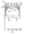
しかし、典型的なAC入力電圧レベルは、(RMSレベルの)分散が大きく、たとえば、110Vが前提とされているのに対して85Vから135Vまでの範囲であるため、上記の問題は世界の多くの地域で重大である。したがって、このような従来技術のデバイスでは、出力輝度が著しく変動し、85Vから135Vまでの範囲では出力光束の変化が3倍になる。出力輝度がこのように変動することは典型的な消費者には受け入れられない。 However, typical AC input voltage levels are highly distributed (RMS level), for example, in the range of 85V to 135V compared to 110V, so the above problem is much more in the world Is serious in the region. Therefore, in such a prior art device, the output luminance varies remarkably, and the change in the output luminous flux is tripled in the range from 85V to 135V. This variation in output brightness is unacceptable to a typical consumer.
標準的なAC入力電圧と一緒に使用される従来技術のデバイスの他の重大な問題は、稼働率が低いことであり、印加されるAC電圧が可変であるため、LEDはACサイクル全体にわたって通電するわけではない。具体的には、ACサイクル中に入力電圧が比較的低くなると、LED電流がなくなり、発光が停止する。たとえば、整流ACサイクルのほぼ中間の3分の1の間のみLED電流が存在し、180度整流ACサイクルの最初の60度および最後の60度の間にはLED電流がなくなる場合がある。このような状況では、LED稼働率は20%程度に低くなることがあり、これは、特に関連するコストが比較的高い場合には非常に低い稼働率である。 Another significant problem with prior art devices used in conjunction with standard AC input voltages is low availability and the applied AC voltage is variable so that the LEDs are energized throughout the AC cycle. Not to do. Specifically, when the input voltage becomes relatively low during the AC cycle, the LED current disappears and light emission stops. For example, there may be LED current only during approximately the middle third of the rectified AC cycle, and there will be no LED current during the first 60 degrees and the last 60 degrees of the 180 degree rectified AC cycle. In such a situation, the LED availability may be as low as 20%, which is very low, especially when the associated costs are relatively high.
消費者用途向けのLEDドライバに対する従来技術の試みには他の多数の問題がある。たとえば、場合によっては、電流のエクスカーションを制限するのに大形の高価な抵抗器を使用する必要が生じ、それに応じて電力が失われ、かなりの電力が失われることがあり、固体照明に切り替える目的の一部が満たせなくなることがある。 There are a number of other problems with prior art attempts at LED drivers for consumer applications. For example, in some cases, it may be necessary to use a large, expensive resistor to limit the current excursion, resulting in a loss of power and considerable power loss and switching to solid state lighting Some objectives may not be met.
したがって、高輝度用途向けのLEDを含む1つまたは複数のLEDにAC線電力を供給し、同時にLEDドライバの全体的な小形化およびコスト削減を実現し、LEDの効率および稼働率を向上させる装置、方法、およびシステムが依然として必要である。このような装置、方法、およびシステムは、比較的広いAC入力電圧範囲にわたって適切に機能し、一方、過度の内部電圧を生成することも構成要素を高い電圧ストレスまたは過度の電圧ストレスにさらすこともなしに、所望の出力電圧または電流を供給することができる必要がある。また、このような装置、方法、およびシステムは、入力電力用のAC線に接続されたときに有効な力率補正を実施する必要がある。また、照明デバイスの輝度、色温度、および色を調節するこのような装置、方法、およびシステムを提供することが望ましい。 Accordingly, an apparatus that provides AC line power to one or more LEDs, including LEDs for high brightness applications, while simultaneously reducing the overall size and cost of the LED driver and improving the efficiency and availability of LEDs , Methods and systems are still needed. Such devices, methods, and systems function properly over a relatively wide AC input voltage range, while generating excessive internal voltages and subjecting components to high or excessive voltage stress. Without being able to supply the desired output voltage or current. Also, such devices, methods, and systems need to perform effective power factor correction when connected to an input power AC line. It would also be desirable to provide such an apparatus, method and system for adjusting the brightness, color temperature, and color of a lighting device.
本発明の例示的な実施形態は、LEDのような非線形負荷への電力の供給に関する多数の利点をもたらす。本発明の様々な例示的な実施形態は、高輝度用途向けのLEDを含む1つまたは複数のLEDにAC線電力を供給し、同時にLEDドライバの全体的な小形化およびコスト削減を実現し、LEDの効率および稼働率を向上させる。例示的な装置実施形態、方法実施形態、およびシステム実施形態は、比較的広いAC入力電圧範囲にわたって適切に適応しかつ機能し、一方、過度の内部電圧を生成することも構成要素を高い電圧ストレスまたは過度の電圧ストレスにさらすこともなしに、所望の出力電圧または電流を供給する。また、様々な例示的な装置実施形態、方法実施形態、およびシステム実施形態は、入力電力用のAC線に接続されたときに有効な力率補正を実施する。例示的な実施形態はまた、LEDの出力でキャパシタンスを大幅に低減させ、それによって信頼性を著しく向上させる。最後に、様々な例示的な装置、方法、およびシステムの実施形態は、輝度、色温度、および照明デバイスの色を調節する機能を実現する。 Exemplary embodiments of the present invention provide a number of advantages related to supplying power to non-linear loads such as LEDs. Various exemplary embodiments of the present invention provide AC line power to one or more LEDs, including LEDs for high brightness applications, while at the same time achieving overall miniaturization and cost reduction of LED drivers, Improve LED efficiency and availability. Exemplary apparatus embodiments, method embodiments, and system embodiments adequately adapt and function over a relatively wide AC input voltage range, while generating excessive internal voltages can also cause high voltage stress on components. Or provide the desired output voltage or current without exposure to excessive voltage stress. Also, the various exemplary apparatus embodiments, method embodiments, and system embodiments perform power factor correction that is effective when connected to an AC line for input power. The exemplary embodiment also significantly reduces capacitance at the output of the LED, thereby significantly improving reliability. Finally, various exemplary apparatus, method, and system embodiments provide the ability to adjust brightness, color temperature, and color of lighting devices.
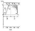
ここで、例示的な実施形態のいくつかの重要な利点を強調する必要がある。第1に、例示的な実施形態は、力率補正を実施することができ、それによって出力輝度がかなり高くなるとともにエネルギーが著しく節約される。第2に、LEDの稼働率がかなり高く、ACサイクルのあらゆる部分の大部分にわたって少なくともいくつかのLEDが使用される。このように稼働率が高いため、LEDの全体的な数を少なくし、それにもかかわらず、より多くのLEDを有する他のデバイスに匹敵する光出力を生成することができる。 Here, some important advantages of the exemplary embodiments need to be emphasized. First, the exemplary embodiment can perform power factor correction, which results in significantly higher output brightness and significant energy savings. Second, the availability of LEDs is quite high and at least some LEDs are used throughout most of every part of the AC cycle. This high availability can reduce the overall number of LEDs and nevertheless produce light output comparable to other devices with more LEDs.
各セグメントが少なくとも1つの発光ダイオードを備え、発光ダイオードの選択されたセグメントを直列発光ダイオード電流経路に含められるように切り替えるかあるいは直列発光ダイオード電流経路から除外されるように切り替えるように対応する複数のスイッチに結合された、発光ダイオードの複数のセグメントを形成するように直列に結合された、AC電力を受け取るように結合可能な複数の発光ダイオードに電力を供給する例示的な方法実施形態が開示される。この例示的な方法実施形態は、第1のパラメータを監視することと、AC電圧間隔の第1の部分の間に、第1のパラメータが第1の所定のレベルに達したときに、発光ダイオードの対応するセグメントを直列発光ダイオード電流経路に含められるように切り替えることと、AC電圧間隔の第2の部分の間に、第1のパラメータが第2の所定のレベルまで低下したときに、発光ダイオードの対応するセグメントを直列発光ダイオード電流経路から除外されるように切り替えることとを含む。 Each segment comprises at least one light-emitting diode, and a plurality of corresponding switches to switch selected segments of the light-emitting diodes to be included or excluded from the series light-emitting diode current path An exemplary method embodiment for powering a plurality of light emitting diodes coupled to a switch and coupled in series to form a plurality of segments of light emitting diodes and coupleable to receive AC power is disclosed. The The exemplary method embodiment includes a light emitting diode when the first parameter reaches a first predetermined level during the monitoring of the first parameter and the first portion of the AC voltage interval. When switching the first segment to a second predetermined level during the switching of the corresponding segment of the LED to be included in the series light emitting diode current path and the second portion of the AC voltage interval. Switching the corresponding segment to be excluded from the series light emitting diode current path.
例示的な実施形態では、第1のパラメータは直列発光ダイオード電流経路の電流レベルである。様々な例示的な実施形態では、この方法は、直列発光ダイオード電流経路の電流レベルを第1の所定のレベルに実質的に一定に維持することを含む。また、様々な例示的な実施形態では、この方法は、AC電圧間隔の第1の部分の間に、第1のパラメータが第3の所定のレベルに達したときに、発光ダイオードの対応する次のセグメントを直列発光ダイオード電流経路に含められるように切り替えることと、AC電圧間隔の第2の部分の間に、第1のパラメータが第4の所定のレベルまで低下したときに、発光ダイオードの対応するセグメントを直列発光ダイオード電流経路から除外されるように切り替えることとをさらに含む。 In the exemplary embodiment, the first parameter is the current level of the series light emitting diode current path. In various exemplary embodiments, the method includes maintaining the current level of the series light emitting diode current path at a first predetermined level substantially constant. Also, in various exemplary embodiments, the method includes a corresponding next step of the light emitting diode when the first parameter reaches a third predetermined level during the first portion of the AC voltage interval. During the second portion of the AC voltage interval and when the first parameter falls to a fourth predetermined level during the switching of the segment to be included in the series light emitting diode current path Switching the segment to be excluded from the series light emitting diode current path.
様々な例示的な方法実施形態は、AC電圧間隔の第1の部分の間に、発光ダイオード電流が連続的に所定のピーク・レベルに達するときに、発光ダイオードの対応するセグメントを直列発光ダイオード電流経路に含められるように連続的に切り替えることと、AC電圧間隔の第2の部分の間に、整流AC電圧レベルが対応する電圧レベルまで低下したときに、発光ダイオードの対応するセグメントを直列発光ダイオード電流経路から除外されるように切り替えることとをさらに含んでもよい。様々な例示的な実施形態では、発光ダイオードの対応するセグメントを直列発光ダイオード電流経路から除外されるように切り替えることは、発光ダイオードの対応するセグメントを直列発光ダイオード電流経路に含められるように切り替えることと逆の順序で行われる。 Various exemplary method embodiments may apply a corresponding segment of light emitting diodes in series light emitting diode current when the light emitting diode current continuously reaches a predetermined peak level during a first portion of the AC voltage interval. During continuous switching to be included in the path and the second part of the AC voltage interval, when the rectified AC voltage level drops to the corresponding voltage level, the corresponding segment of the light emitting diode is connected in series And switching to be excluded from the current path. In various exemplary embodiments, switching the corresponding segment of the light emitting diode to be excluded from the series light emitting diode current path switches the corresponding segment of the light emitting diode to be included in the series light emitting diode current path. And in the reverse order.
例示的な実施形態では、時間または時間間隔をパラメータとして利用することができる。たとえば、第1のパラメータおよび第2のパラメータは時間であっても、1つまたは複数の時間間隔であっても、時間ベースのパラメータであっても、1つまたは複数のクロック・サイクル・カウントであってもよい。また、たとえば、例示的な方法実施形態は、AC電圧間隔の第1の部分用の発光ダイオードのセグメントの数に対応する第1の複数の時間間隔を求めることと、AC電圧間隔の第2の部分用の発光ダイオードのセグメントの数に対応する第2の複数の時間間隔を求めることとをさらに含んでよい。このような例示的な実施形態では、この方法は、AC電圧間隔の第1の部分の間に、第1の複数の時間間隔の各時間間隔が満了したときに、発光ダイオードの次のセグメントを直列発光ダイオード電流経路に含められるように切り替えることと、AC電圧間隔の第2の部分の間に、第2の複数の時間間隔の各時間間隔が満了したときに、発光ダイオードの次のセグメントを直列発光ダイオード電流経路から除外されるように切り替えることとをさらに含んでよい。 In an exemplary embodiment, time or time interval can be utilized as a parameter. For example, the first parameter and the second parameter may be time, one or more time intervals, time-based parameters, one or more clock cycle counts. There may be. Also, for example, the exemplary method embodiment may determine a first plurality of time intervals corresponding to the number of light emitting diode segments for the first portion of the AC voltage interval and a second of the AC voltage interval. Determining a second plurality of time intervals corresponding to the number of segments of the partial light emitting diodes. In such an exemplary embodiment, the method includes determining a next segment of light emitting diodes during a first portion of the AC voltage interval when each time interval of the first plurality of time intervals expires. Between switching to include in the series light emitting diode current path and the second portion of the AC voltage interval, when each time interval of the second plurality of time intervals expires, the next segment of the light emitting diode is Switching to be excluded from the series light emitting diode current path.
様々な例示的な方法実施形態は、調光器スイッチなどによってAC電圧が位相変調されているかどうかを判定することをさらに含んでもよい。このような例示的な方法実施形態は、AC電圧が位相変調されているときに、位相変調されたAC電圧レベルに対応する発光ダイオードのセグメントを直列発光ダイオード電流経路に含められるように切り替えるか、あるいはAC電圧が位相変調されているときに、位相変調されたAC電圧レベルの時間間隔に対応する発光ダイオードのセグメントを直列発光ダイオード電流経路に含められるように切り替えることをさらに含んでよい。また、例示的な方法実施形態は、AC電圧が位相変調されているときに、発光ダイオードの次のセグメントを第2のスイッチによって直列発光ダイオード電流経路に含められるように切り替えるのと同時に第1のスイッチによって並列発光ダイオード電流経路を維持することをさらに含んでよい。 Various exemplary method embodiments may further include determining whether the AC voltage is phase modulated, such as by a dimmer switch. Such an exemplary method embodiment switches when the AC voltage is phase modulated so that a segment of light emitting diodes corresponding to the phase modulated AC voltage level can be included in the series light emitting diode current path, or Alternatively, when the AC voltage is phase modulated, the method may further comprise switching the light emitting diode segments corresponding to the time interval of the phase modulated AC voltage level to be included in the series light emitting diode current path. The exemplary method embodiment also provides that the first segment at the same time the second segment of the light emitting diode is switched to be included in the series light emitting diode current path by the second switch when the AC voltage is phase modulated. The method may further comprise maintaining a parallel light emitting diode current path by the switch.
様々な例示的な実施形態は、AC電圧が位相変調されているかどうかを判定することをさらに含んでもよい。この方法は、AC電圧が位相変調されているときに、位相変調されたAC電圧レベルに対応する発光ダイオードのセグメントを直列発光ダイオード電流経路に含められるように切り替えるか、AC電圧が位相変調されているときに、位相変調されたAC電流レベルに対応する発光ダイオードのセグメントを直列発光ダイオード電流経路に含められるように切り替えるか、AC電圧が位相変調されているときに、位相変調されたAC電圧の時間間隔に対応する発光ダイオードのセグメントを直列発光ダイオード電流経路に含められるように切り替えるか、あるいはAC電圧が位相変調されているときに、発光ダイオードの次のセグメントを第2のスイッチによって直列発光ダイオード電流経路に含められるように切り替えるのと同時に第1のスイッチによって並列発光ダイオード電流経路を維持することをさらに含んでよい。 Various exemplary embodiments may further include determining whether the AC voltage is phase modulated. This method can either switch the segment of the light emitting diode corresponding to the phase modulated AC voltage level to be included in the series light emitting diode current path when the AC voltage is phase modulated, or the AC voltage is phase modulated. Switch the segment of the light emitting diode corresponding to the phase modulated AC current level to be included in the series light emitting diode current path, or the phase modulated AC voltage when the AC voltage is phase modulated. The segment of the light emitting diode corresponding to the time interval is switched to be included in the series light emitting diode current path, or when the AC voltage is phase modulated, the next light emitting diode segment is switched by the second switch to the series light emitting diode. At the same time as switching to include in the current path, It may further comprise maintaining the parallel light-emitting diode current path by pitch.
様々な例示的な実施形態は、力率補正を実施することもできる。このような例示的な方法実施形態は、発光ダイオードの次のセグメントを直列発光ダイオード電流経路に含められるように切り替えた場合に発光ダイオード電流が所定のピーク・レベルに達するのに十分な時間がAC電圧間隔の第1の部分に残っているかどうかを判定することと、発光ダイオード電流が所定のピーク・レベルに達するのに十分な時間がAC電圧間隔の第1の部分に残っているときに、発光ダイオードの次のセグメントを直列発光ダイオード電流経路に含められるように切り替えることとをさらに含んでよい。同様に、この例示的な方法実施形態は、発光ダイオード電流が所定のピーク・レベルに達するのに十分な時間がAC電圧間隔の第1の部分に残っていないときに、発光ダイオードの次のセグメントを直列発光ダイオード電流経路に含められるように切り替えないことをさらに含んでよい。 Various exemplary embodiments can also implement power factor correction. Such an exemplary method embodiment is such that when the next segment of light emitting diodes is switched to be included in the series light emitting diode current path, sufficient time for the light emitting diode current to reach a predetermined peak level is AC. Determining whether it remains in the first part of the voltage interval and when sufficient time remains in the first part of the AC voltage interval for the light emitting diode current to reach a predetermined peak level, And switching the next segment of light emitting diodes to be included in the series light emitting diode current path. Similarly, this exemplary method embodiment provides for the next segment of light emitting diodes when there is not enough time left in the first part of the AC voltage interval for the light emitting diode current to reach a predetermined peak level. May not be switched to be included in the series light emitting diode current path.
また、様々な例示的な実施形態では、この方法は、発光ダイオードの複数のセグメントを第1の直列発光ダイオード電流経路を形成するように切り替えることと、発光ダイオードの複数のセグメントを、第1の直列発光ダイオード電流経路と並列に第2の直列発光ダイオード電流経路を形成するように切り替えることとをさらに含んでよい。 Also, in various exemplary embodiments, the method switches the plurality of segments of light emitting diodes to form a first series light emitting diode current path, and the plurality of segments of light emitting diodes are switched to the first segment. And switching to form a second series light emitting diode current path in parallel with the series light emitting diode current path.
例示的な実施形態では、発光ダイオードの複数のセグメントのうちの発光ダイオードの選択されたセグメントはそれぞれ、異なる色または波長の発光スペクトルを有する発光ダイオードを備えてよい。このような例示的な実施形態では、この方法は、発光ダイオードの選択されたセグメントを選択的に直列発光ダイオード電流経路に含められるように切り替えて、対応する照明効果を実現し、かつ/あるいは発光ダイオードの選択されたセグメントを選択的に直列発光ダイオード電流経路に含められるように切り替えて、対応する色温度を実現することをさらに含んでよい。 In an exemplary embodiment, each selected segment of the light emitting diodes of the plurality of segments of light emitting diodes may comprise a light emitting diode having an emission spectrum of a different color or wavelength. In such an exemplary embodiment, the method switches selected segments of the light emitting diodes to be selectively included in the series light emitting diode current path to achieve a corresponding lighting effect and / or light emission. The method may further include switching selected segments of the diode to be selectively included in the series light emitting diode current path to achieve a corresponding color temperature.
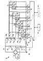
例示的な実施形態では、AC電圧を受け取るように結合可能な装置であって、整流AC電圧を生成する整流器と、発光ダイオードの複数のセグメントを形成するように直列に結合された複数の発光ダイオードと、発光ダイオードの選択されたセグメントを直列発光ダイオード電流経路に含められるように切り替えるかあるいは直列発光ダイオード電流経路から除外されるように切り替えるように発光ダイオードの複数のセグメントに対応して結合された複数のスイッチと、発光ダイオード電流レベルを検知する電流センサと、複数のスイッチおよび電流センサに結合され、整流AC電圧間隔の第1の部分の間に、発光ダイオード電流レベルが第1の所定の電流レベルまで上昇したときに、発光ダイオードの対応するセグメントを直列発光ダイオード電流経路に含められるように切り替え、整流AC電圧間隔の第2の部分の間に、発光ダイオード電流レベルが第2の所定の電流レベルまで低下したときに、発光ダイオードの対応するセグメントを直列発光ダイオード電流経路から除外されるように切り替えるコントローラとを備える装置が開示される。 In an exemplary embodiment, a device that can be coupled to receive an AC voltage, the rectifier generating a rectified AC voltage, and a plurality of light emitting diodes coupled in series to form a plurality of segments of light emitting diodes. And correspondingly coupled to the plurality of segments of the light emitting diode to switch the selected segment of the light emitting diode to be included in the series light emitting diode current path or to be excluded from the series light emitting diode current path. A plurality of switches, a current sensor for sensing a light emitting diode current level, and a plurality of switches and a current sensor coupled to the first portion of the rectified AC voltage interval, the light emitting diode current level is a first predetermined current. When the level rises, the corresponding segment of the light emitting diode is connected to the series light emitting die. Switch to be included in the diode current path, and during the second portion of the rectified AC voltage interval, when the LED current level drops to a second predetermined current level, the corresponding segment of the LED is serially connected. An apparatus is disclosed comprising a controller that switches to be excluded from a light emitting diode current path.
例示的な実施形態では、コントローラはさらに、発光ダイオード電流レベルを第1の所定のレベルに実質的に一定に維持する。AC電圧間隔の第1の部分の間に、発光ダイオード電流レベルが第3の所定のレベルに達したときに、コントローラはさらに、発光ダイオードの対応する次のセグメントを直列発光ダイオード電流経路に含められるように切り替え、AC電圧間隔の第2の部分の間に、発光ダイオード電流レベルが第4の所定のレベルまで低下したときに、コントローラはさらに、発光ダイオードの対応するセグメントを直列発光ダイオード電流経路から除外されるように切り替える。 In the exemplary embodiment, the controller further maintains the light emitting diode current level substantially constant at a first predetermined level. When the light emitting diode current level reaches a third predetermined level during the first portion of the AC voltage interval, the controller can further include a corresponding next segment of light emitting diodes in the series light emitting diode current path. When the light emitting diode current level drops to a fourth predetermined level during the second portion of the AC voltage interval, the controller further removes the corresponding segment of the light emitting diode from the series light emitting diode current path. Switch to be excluded.
このような例示的な装置実施形態では、この装置は、各々が複数のスイッチのうちの対応するスイッチに直列に結合された複数の抵抗器をさらに備えてよい。各抵抗器は、対応するスイッチの高電圧側に結合されても、あるいは対応するスイッチの低電圧側に結合されてもよい。この例示的な装置は、発光ダイオードの複数のセグメントのうちの発光ダイオードの少なくとも1つのセグメントと直列に結合されたスイッチおよび抵抗器をさらに備えてよい。 In such exemplary device embodiments, the device may further comprise a plurality of resistors, each coupled in series with a corresponding one of the plurality of switches. Each resistor may be coupled to the high voltage side of the corresponding switch, or may be coupled to the low voltage side of the corresponding switch. The exemplary apparatus may further comprise a switch and a resistor coupled in series with at least one segment of the light emitting diodes of the plurality of segments of light emitting diodes.
例示的な実施形態では、発光ダイオードの複数のセグメントのうちの発光ダイオードの最後のセグメントは常に、直列発光ダイオード電流経路に結合される。コントローラはさらに、対応するノード電圧レベルを受け取るように発光ダイオードの複数のセグメントに結合されてもよい。例示的な他の実施形態では、複数のスイッチのうちの少なくとも1つのスイッチが整流AC電圧を受け取るように整流器に結合される。 In the exemplary embodiment, the last segment of the plurality of segments of light emitting diodes is always coupled to the series light emitting diode current path. The controller may further be coupled to a plurality of segments of light emitting diodes to receive corresponding node voltage levels. In another exemplary embodiment, at least one of the plurality of switches is coupled to the rectifier to receive the rectified AC voltage.
例示的な他の装置実施形態では、整流AC電圧間隔の第1の部分の間に、発光ダイオード電流レベルが所定のピーク・レベルに達するときに、コントローラはさらに、整流AC電圧レベルの対応する値を求めて記憶し、発光ダイオードの対応するセグメントを直列発光ダイオード電流経路に含められるように連続的に切り替えてよく、かつ整流AC電圧間隔の第2の部分の間に、整流AC電圧レベルが対応する値まで低下したときに、コントローラはさらに、発光ダイオードの対応するセグメントを直列発光ダイオード電流経路から除外されるように切り替え、この切り替えを、発光ダイオードの対応するセグメントを直列発光ダイオード電流経路に含められるように切り替えることと逆の順序で行ってよい。 In another exemplary apparatus embodiment, when the light emitting diode current level reaches a predetermined peak level during the first portion of the rectified AC voltage interval, the controller further includes a corresponding value of the rectified AC voltage level. The corresponding segment of the light emitting diode may be continuously switched to be included in the series light emitting diode current path, and the rectified AC voltage level corresponds during the second portion of the rectified AC voltage interval The controller further switches the corresponding segment of the light emitting diode to be excluded from the series light emitting diode current path, and includes this switching in the series light emitting diode current path. May be performed in the reverse order of switching.
様々な例示的な実施形態では、コントローラはさらに、整流AC電圧が位相変調されているかどうかを判定してよい。このような例示的な方法実施形態では、コントローラは、整流AC電圧が位相変調されているときに、さらに、整流AC電圧レベルに対応する発光ダイオードのセグメントを直列発光ダイオード電流経路に含められるように切り替えるか、あるいは整流AC電圧レベルの時間間隔に対応する発光ダイオードのセグメントを直列発光ダイオード電流経路に含められるように切り替えてよい。例示的な他の装置実施形態では、コントローラは、整流AC電圧が位相変調されているときに、さらに、発光ダイオードの次のセグメントを第2のスイッチによって直列発光ダイオード電流経路に含められるように切り替えるのと同時に第1のスイッチによって並列発光ダイオード電流経路を維持してよい。 In various exemplary embodiments, the controller may further determine whether the rectified AC voltage is phase modulated. In such exemplary method embodiments, the controller can further include a segment of light emitting diodes corresponding to the rectified AC voltage level in the series light emitting diode current path when the rectified AC voltage is phase modulated. Alternatively, the LED segments corresponding to the time interval of the rectified AC voltage level may be switched so that they are included in the series LED current path. In another exemplary device embodiment, the controller further switches the next segment of light emitting diodes to be included in the series light emitting diode current path by the second switch when the rectified AC voltage is phase modulated. At the same time, the parallel light emitting diode current path may be maintained by the first switch.
様々な例示的な実施形態では、コントローラは、ある形態の力率補正を実施することもできる。このような例示的な装置実施形態では、コントローラはさらに、発光ダイオードの次のセグメントを直列発光ダイオード電流経路に含められるように切り替えた場合に発光ダイオード電流レベルが所定のピーク・レベルに達するのに十分な時間が整流AC電圧間隔の第1の部分に残っているかどうかを判定してよい。このような例示的な実施形態では、発光ダイオード電流レベルが所定のピーク・レベルに達するのに十分な時間が整流AC電圧間隔の第1の部分に残っているときに、コントローラはさらに、発光ダイオードの次のセグメントを直列発光ダイオード電流経路に含められるように切り替えてよく、かつ発光ダイオード電流レベルが所定のピーク・レベルに達するのに十分な時間が整流AC電圧間隔の第1の部分に残っていないときに、コントローラはさらに、発光ダイオードの次のセグメントを直列発光ダイオード電流経路に含められるように切り替えなくてよい。 In various exemplary embodiments, the controller may also perform some form of power factor correction. In such an exemplary device embodiment, the controller further causes the light emitting diode current level to reach a predetermined peak level when the next segment of the light emitting diode is switched to be included in the series light emitting diode current path. It may be determined whether sufficient time remains in the first portion of the rectified AC voltage interval. In such an exemplary embodiment, the controller further includes the light emitting diode when sufficient time remains in the first portion of the rectified AC voltage interval for the light emitting diode current level to reach a predetermined peak level. Of the next segment may be switched to be included in the series LED current path, and sufficient time remains in the first portion of the rectified AC voltage interval for the LED current level to reach a predetermined peak level. When not, the controller may also not switch to allow the next segment of light emitting diodes to be included in the series light emitting diode current path.
例示的な他の実施形態では、コントローラはさらに、発光ダイオードの複数のセグメントを第1の直列発光ダイオード電流経路を形成するように切り替え、発光ダイオードの複数のセグメントを、第1の直列発光ダイオード電流経路と並列に第2の直列発光ダイオード電流経路を形成するように切り替える。 In another exemplary embodiment, the controller further switches the plurality of segments of light emitting diodes to form a first series light emitting diode current path, wherein the plurality of segments of light emitting diodes are switched to the first series light emitting diode current. Switching to form a second series light emitting diode current path in parallel with the path.
様々な例示的な実施形態では、この装置は、実質的に約100Hz、120Hz、300Hz、360Hz、または400Hzの整流AC電圧周波数で動作してよい。また、この装置は、各々が複数の発光ダイオードのうちの対応する発光ダイオードに結合され、かつ各々の発光減衰時定数が約2msecから3msecの間である複数の蛍光体コーティングまたは蛍光体層をさらに備えてよい。 In various exemplary embodiments, the device may operate at a rectified AC voltage frequency substantially of about 100 Hz, 120 Hz, 300 Hz, 360 Hz, or 400 Hz. The apparatus further includes a plurality of phosphor coatings or phosphor layers each coupled to a corresponding one of the plurality of light emitting diodes and each having an emission decay time constant between about 2 msec and 3 msec. You may be prepared.
例示的な他の装置は、AC電圧を受け取るように結合可能であり、発光ダイオードの第1の複数のセグメントを形成するように直列に結合された第1の複数の発光ダイオードと、制御信号に応答して、発光ダイオードの選択されたセグメントを第1の直列発光ダイオード電流経路に含められるように切り替えるかあるいは第1の直列発光ダイオード電流経路から除外されるように切り替えるように発光ダイオードの第1の複数のセグメントに結合された第1の複数のスイッチと、発光ダイオード電流レベルを検知する電流センサと、複数のスイッチおよび電流センサに結合され、AC電圧間隔の第1の部分の間に、発光ダイオード電流レベルに応答して、第1の制御信号を生成し、発光ダイオードの第1の複数のセグメントのうちの発光ダイオードの対応するセグメントを第1の直列発光ダイオード電流経路に含められるように切り替え、AC電圧間隔の第2の部分の間に、発光ダイオード電流レベルに応答して、発光ダイオードの第1の複数のセグメントのうちの発光ダイオードの対応するセグメントを第1の直列発光ダイオード電流経路から除外されるように切り替えるコントローラとを備える装置である。 Another exemplary device is coupleable to receive an AC voltage, a first plurality of light emitting diodes coupled in series to form a first plurality of segments of light emitting diodes, and a control signal In response, a first segment of the light emitting diode is switched to switch the selected segment of the light emitting diode to be included in the first series light emitting diode current path or to be excluded from the first series light emitting diode current path. A first plurality of switches coupled to the plurality of segments, a current sensor for sensing a light emitting diode current level, and a light emitting during a first portion of the AC voltage interval coupled to the plurality of switches and the current sensor. In response to the diode current level, a first control signal is generated and the light emitting die of the first plurality of segments of the light emitting diode A first segment of the light emitting diode in response to the light emitting diode current level during the second portion of the AC voltage interval. And a controller for switching a corresponding segment of the light emitting diodes of the segments to be excluded from the first series light emitting diode current path.
例示的な装置実施形態では、この装置は、発光ダイオードの第2の複数のセグメントを形成するように直列に結合された第2の複数の発光ダイオードと、発光ダイオードの第2の複数のセグメントのうちの選択されたセグメントを第2の直列発光ダイオード電流経路に含められるように切り替えるかあるいは第2の直列発光ダイオード電流経路から除外されるように切り替えるように発光ダイオードの第2の複数のセグメントに結合された第2の複数のスイッチとをさらに備えてよく、その場合、コントローラはさらに、第2の複数のスイッチに結合され、さらに、対応する制御信号を生成して、発光ダイオードの第2の複数のセグメントのうちの複数のセグメントを、第1の直列発光ダイオード電流経路に並列に第2の直列発光ダイオード電流経路を形成するように切り替える。第2の直列発光ダイオード電流経路は、第1の直列発光ダイオード電流経路と逆の極性を有してよいか、あるいは第1の直列発光ダイオード電流経路を通る第1の電流の流れが、第2の直列発光ダイオード電流経路を通る第2の電流の流れとは逆の方向を有する。 In an exemplary apparatus embodiment, the apparatus includes a second plurality of light emitting diodes coupled in series to form a second plurality of segments of light emitting diodes, and a second plurality of segments of light emitting diodes. The selected plurality of segments are switched to be included in the second series light emitting diode current path, or switched to be excluded from the second series light emitting diode current path. A second plurality of switches coupled, wherein the controller is further coupled to the second plurality of switches and further generates a corresponding control signal to generate a second LED of the light emitting diode. A plurality of segments of the plurality of segments are connected in parallel to the first series light emitting diode current path, and the second series light emitting diode Switching so as to form a flow path. The second series light emitting diode current path may have an opposite polarity to the first series light emitting diode current path, or the first current flow through the first series light emitting diode current path is the second Having a direction opposite to the second current flow through the series light emitting diode current path.
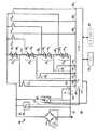
様々な例示的な実施形態のうちの他の実施形態では、この装置は、電流制限回路、調光インタフェース回路、コントローラに結合されたDC電源回路、および/または温度保護回路をさらに備えてよい。 In other embodiments of the various exemplary embodiments, the apparatus may further comprise a current limiting circuit, a dimming interface circuit, a DC power supply circuit coupled to the controller, and / or a temperature protection circuit.
各々が少なくとも1つの発光ダイオードを備える発光ダイオードの複数のセグメントを形成するように直列に結合され、発光ダイオードの選択されたセグメントを直列発光ダイオード電流経路に含められるように切り替えるかあるいは直列発光ダイオード電流経路から除外されるように切り替えるように、発光ダイオードの複数のセグメントが対応する複数のスイッチに結合された、AC電圧を受け取るように結合可能な複数の発光ダイオードに電力を供給する他の例示的な方法実施形態が開示される。この例示的な方法実施形態は、AC電圧間隔の第1の部分の間に第1のパラメータに応答して、第2のパラメータの値を求めて記憶し、発光ダイオードの対応するセグメントを直列発光ダイオード電流経路に含められるように切り替えることと、AC電圧間隔の第2の部分の間、第2のパラメータを監視し、第2のパラメータの現在の値が記憶されている値と実質的に等しいときに、発光ダイオードの対応するセグメントを直列発光ダイオード電流経路から除外されるように切り替えることとを含む。 Coupled in series to form a plurality of segments of light emitting diodes each comprising at least one light emitting diode, switching selected segments of the light emitting diodes to be included in the series light emitting diode current path, or series light emitting diode currents Other exemplary power supplies to a plurality of light emitting diodes that can be coupled to receive an AC voltage, wherein the segments of the light emitting diodes are coupled to corresponding switches to switch out of the path. A method embodiment is disclosed. The exemplary method embodiment determines and stores a value of a second parameter in response to the first parameter during a first portion of the AC voltage interval and serially emits a corresponding segment of the light emitting diode. During the second portion of the AC voltage interval and switching to be included in the diode current path, the second parameter is monitored and the current value of the second parameter is substantially equal to the stored value Sometimes switching the corresponding segment of the light emitting diode to be excluded from the series light emitting diode current path.
例示的な実施形態では、AC電圧は整流AC電圧を含み、例示的な方法は、整流AC電圧が実質的に零に近い時点を判定することと、同期信号を生成することとをさらに含む。例示的な方法は、整流AC電圧が実質的に零に近い時点を少なくとも1回判定することによってAC電圧間隔を求めることをさらに含んでよい。 In an exemplary embodiment, the AC voltage includes a rectified AC voltage, and the exemplary method further includes determining when the rectified AC voltage is substantially near zero and generating a synchronization signal. The exemplary method may further include determining the AC voltage interval by determining at least once when the rectified AC voltage is substantially near zero.
様々な例示的な実施形態では、この方法は、AC電圧を整流して整流AC電圧を生成することをさらに含んでよい。たとえば、このような例示的な実施形態では、第1のパラメータは発光ダイオード電流レベルであってよく、第2のパラメータは整流AC入力電圧レベルであってよい。たとえば、LED電流レベル、ピークLED電流レベル、電圧レベル、光学輝度レベルを含む、パラメータの他の組み合わせも請求される発明の範囲内である。このような例示的な実施形態では、この方法は、AC電圧間隔の第1の部分の間に発光ダイオード電流レベルが所定のピーク値に達したときに、整流AC入力電圧レベルの第1の値を求めて記憶し、発光ダイオードの第1のセグメントを直列発光ダイオード電流経路に含められるように切り替えることと、発光ダイオード電流レベルを監視することと、その後、発光ダイオード電流がAC電圧間隔の第1の部分の間に所定のピーク値に達したときに、整流AC入力電圧レベルの第2の値を求めて記憶し、発光ダイオードの第2のセグメントを直列発光ダイオード電流経路に含められるように切り替えることとをさらに含んでよい。(このような所定の値は、事前にオフラインで指定するか、または事前に、直前のACサイクル中のような回路の動作中に指定または算出するような様々な方法で求められてよい)。この例示的な方法は、整流AC電圧レベルを監視することと、整流AC電圧レベルが、AC電圧間隔の第2の部分の間に第2の値に達したときに、発光ダイオードの第2のセグメントを直列発光ダイオード電流経路から除外されるように切り替えることと、整流AC電圧レベルが、AC電圧間隔の第2の部分の間に第1の値に達したときに、発光ダイオードの第1のセグメントを直列発光ダイオード電流経路から除外されるように切り替えることとをさらに含んでもよい。 In various exemplary embodiments, the method may further include rectifying the AC voltage to generate a rectified AC voltage. For example, in such an exemplary embodiment, the first parameter may be a light emitting diode current level and the second parameter may be a rectified AC input voltage level. Other combinations of parameters are also within the scope of the claimed invention, including, for example, LED current level, peak LED current level, voltage level, and optical brightness level. In such an exemplary embodiment, the method includes a first value of the rectified AC input voltage level when the light emitting diode current level reaches a predetermined peak value during a first portion of the AC voltage interval. And switching to allow the first segment of light emitting diodes to be included in the series light emitting diode current path, monitoring the light emitting diode current level, and then the light emitting diode current to the first of the AC voltage interval. When a predetermined peak value is reached during the portion of, a second value of the rectified AC input voltage level is determined and stored, and the second segment of light emitting diodes is switched to be included in the series light emitting diode current path. May further include. (Such a predetermined value may be determined in advance in various ways, such as being specified offline in advance, or specified or calculated in advance during operation of the circuit, such as during the previous AC cycle). The exemplary method monitors the rectified AC voltage level and determines when the rectified AC voltage level reaches a second value during the second portion of the AC voltage interval. Switching the segment to be excluded from the series light emitting diode current path and the first of the light emitting diodes when the rectified AC voltage level reaches a first value during the second portion of the AC voltage interval. Switching the segment to be excluded from the series light emitting diode current path.
また、様々な例示的な実施形態では、この方法は、AC電圧間隔の第1の部分の間に、発光ダイオード電流が首尾よく所定のピーク・レベルに達したときに、整流AC電圧レベルの対応する値を求めて記憶し、発光ダイオードの対応するセグメントを直列発光ダイオード電流経路に含められるように切り替えることと、AC電圧間隔の第2の部分の間に、整流AC電圧レベルが対応する電圧レベルまで低下したときに、発光ダイオードの対応するセグメントを直列発光ダイオード電流経路から除外されるように切り替えることとをさらに含んでよい。このような例示的な方法実施形態では、発光ダイオードの対応するセグメントを直列発光ダイオード電流経路から除外されるように切り替えることは、発光ダイオードの対応するセグメントを直列発光ダイオード電流経路に含められるように切り替えることと逆の順序であってよい。 Also, in various exemplary embodiments, the method also provides a response to the rectified AC voltage level when the light emitting diode current successfully reaches a predetermined peak level during the first portion of the AC voltage interval. A value to which the rectified AC voltage level corresponds between the second part of the AC voltage interval and switching the corresponding segment of the light emitting diode to be included in the series light emitting diode current path And switching the corresponding segment of the light emitting diode to be excluded from the series light emitting diode current path when reduced to. In such exemplary method embodiments, switching the corresponding segment of the light emitting diode to be excluded from the series light emitting diode current path is such that the corresponding segment of the light emitting diode is included in the series light emitting diode current path. It may be the reverse order of switching.
他の例示的な実施形態では、この方法は、発光ダイオード電流がAC電圧間隔の第1の部分の間に所定のピーク・レベルに達したときに、整流AC入力電圧レベルの第1の値を求めて記憶することと、整流AC入力電圧レベルの第1の値が実質的に所定の電圧しきい値以上であるときに、発光ダイオードの対応するセグメントを直列発光ダイオード電流経路に含められるように切り替えることとをさらに含んでよい。 In another exemplary embodiment, the method provides a first value for the rectified AC input voltage level when the light emitting diode current reaches a predetermined peak level during the first portion of the AC voltage interval. Determining and storing and, when the first value of the rectified AC input voltage level is substantially greater than or equal to a predetermined voltage threshold, a corresponding segment of the light emitting diode can be included in the series light emitting diode current path. Switching may further be included.
様々な例示的な実施形態では、この方法は、発光ダイオード電流レベルを監視することと、AC電圧間隔の第2の部分の間に、発光ダイオード電流レベルが所定のピーク・レベルよりも所定のマージンだけ高いときに、第2のパラメータの新しい値を求めて記憶し、発光ダイオードの対応するセグメントを直列発光ダイオード電流経路に含められるように切り替えることとをさらに含んでよい。 In various exemplary embodiments, the method includes monitoring a light emitting diode current level and a second margin of the light emitting diode current level from a predetermined peak level during a second portion of the AC voltage interval. And determining and storing the new value of the second parameter when it is high, and switching the corresponding segment of the light emitting diode to be included in the series light emitting diode current path.
例示的な他の方法実施形態では、この方法は、発光ダイオードの複数のセグメントを第1の直列発光ダイオード電流経路を形成するように切り替えることと、発光ダイオードの複数のセグメントを、第1の直列発光ダイオード電流経路に並列に第2の直列発光ダイオード電流経路を形成するように切り替えることとをさらに含んでよい。 In another exemplary method embodiment, the method switches the plurality of segments of light emitting diodes to form a first series light emitting diode current path and the plurality of segments of light emitting diodes in a first series. And switching to form a second series light emitting diode current path in parallel with the light emitting diode current path.
様々な例示的な実施形態は、第1の直列発光ダイオード電流経路がACサイクルの正の部分の間に通電するときに、ACサイクルの負の部分の間に通電することなどのために第1の直列発光ダイオード電流経路とは逆の方向および極性を有する第2の直列発光ダイオード電流経路を実現してもよい。このような例示的な実施形態では、この方法は、AC電圧間隔の第3の部分の間に、発光ダイオードの第2の複数のセグメントを、AC電圧間隔の第1の部分に形成される直列発光ダイオード電流経路とは逆の極性を有する第2の直列発光ダイオード電流経路を形成するように切り替えることと、AC電圧間隔の第4の部分の間に、発光ダイオードの第2の複数のセグメントを第2の直列発光ダイオード電流経路から除外されるように切り替えることとをさらに含んでよい。 Various exemplary embodiments provide a first such as energizing during the negative portion of the AC cycle, such as when the first series light emitting diode current path is energized during the positive portion of the AC cycle. A second series light emitting diode current path having a direction and polarity opposite to the series light emitting diode current path may be realized. In such an exemplary embodiment, the method includes a series of second plurality of light emitting diodes formed in the first portion of the AC voltage interval during the third portion of the AC voltage interval. During the fourth portion of the AC voltage interval, the second plurality of segments of the light emitting diode are switched between forming a second series light emitting diode current path having a polarity opposite to that of the light emitting diode current path. Switching to be excluded from the second series light emitting diode current path.
例示的な他の実施形態は、AC電圧を受け取るように結合可能な装置である。例示的な装置は、整流AC電圧レベルを生成する整流器と、発光ダイオードの複数のセグメントを形成するように直列に結合された複数の発光ダイオードと、発光ダイオードの選択されたセグメントを直列発光ダイオード電流経路に含められるように切り替えるかあるいは直列発光ダイオード電流経路から除外されるように切り替えるように発光ダイオードの複数のセグメントに対応して結合された複数のスイッチと、発光ダイオード電流レベルを検知する電流センサと、整流AC電圧レベルを検知する電圧センサと、複数のパラメータを記憶するメモリと、複数のスイッチ、メモリ、電流センサ、および電圧センサに結合され、AC電圧間隔の第1の部分の間に、発光ダイオード電流レベルが所定のピーク発光ダイオード電流レベルに達したときに、整流AC電圧レベルの対応する値を求めてメモリに記憶し、発光ダイオードの対応するセグメントを直列発光ダイオード電流経路に含められるように切り替え、整流AC電圧間隔の第2の部分の間、整流AC電圧レベルを監視し、整流AC電圧レベルの現在の値が整流AC電圧レベルの記憶されている対応する値に実質的に等しいときに、発光ダイオードの対応するセグメントを直列発光ダイオード電流経路から除外されるように切り替えるコントローラとを備える。 Another exemplary embodiment is a device that can be coupled to receive an AC voltage. An exemplary apparatus includes a rectifier that generates a rectified AC voltage level, a plurality of light emitting diodes coupled in series to form a plurality of segments of light emitting diodes, and a selected segment of light emitting diodes in series light emitting diode current. A plurality of switches coupled to correspond to the plurality of segments of the light emitting diodes to be switched to be included in the path or to be excluded from the series light emitting diode current path, and a current sensor for detecting the light emitting diode current level And a voltage sensor that senses a rectified AC voltage level, a memory that stores a plurality of parameters, a plurality of switches, a memory, a current sensor, and a voltage sensor, and during a first portion of the AC voltage interval, The LED current level reaches the predetermined peak LED current level. Sometimes the corresponding value of the rectified AC voltage level is determined and stored in memory, the corresponding segment of the light emitting diode is switched to be included in the series light emitting diode current path, and during the second part of the rectified AC voltage interval, When the rectified AC voltage level is monitored and the current value of the rectified AC voltage level is substantially equal to the stored corresponding value of the rectified AC voltage level, the corresponding segment of the light emitting diode is removed from the series light emitting diode current path. And a controller that switches to be excluded.
このような例示的な装置実施形態では、整流AC電圧レベルが実質的に零に近いときに、コントローラはさらに、対応する同期信号を生成する。様々な例示的な実施形態では、コントローラはさらに、整流AC電圧レベルは実質的に零に近いことを少なくとも1回判定することによって整流AC電圧間隔を求めてよい。 In such exemplary device embodiments, the controller further generates a corresponding synchronization signal when the rectified AC voltage level is substantially near zero. In various exemplary embodiments, the controller may further determine the rectified AC voltage interval by determining at least once that the rectified AC voltage level is substantially near zero.
例示的な実施形態では、発光ダイオード電流レベルが整流AC電圧間隔の第1の部分の間に、発光ダイオード電流レベルが所定のピーク発光ダイオード電流レベルに達したときに、コントローラはさらに、整流AC電圧レベルの第1の値を求めてメモリに記憶し、発光ダイオードの第1のセグメントを直列発光ダイオード電流経路に含められるように切り替え、発光ダイオード電流レベルを監視し、その後、発光ダイオード電流レベルが、整流AC電圧レベルの第1の部分の間に所定のピーク発光ダイオード電流レベルに達したときに、コントローラはさらに、整流AC電圧レベルの第2の値を求めてメモリに記憶し、発光ダイオードの第2のセグメントを直列発光ダイオード電流経路に含められるように切り替える。 In an exemplary embodiment, when the light emitting diode current level reaches a predetermined peak light emitting diode current level during the first portion of the rectified AC voltage interval, the controller further includes a rectified AC voltage. A first value of the level is determined and stored in the memory, the first segment of the light emitting diode is switched to be included in the series light emitting diode current path, the light emitting diode current level is monitored, and then the light emitting diode current level is When the predetermined peak light emitting diode current level is reached during the first portion of the rectified AC voltage level, the controller further determines a second value of the rectified AC voltage level and stores it in memory to The two segments are switched to be included in the series light emitting diode current path.
このような例示的な装置実施形態では、コントローラはさらに、整流AC電圧レベルを監視し、整流AC電圧レベルが整流AC電圧間隔の第2の部分の間に記憶されている第2の値に達したときに、発光ダイオードの第2のセグメントを直列発光ダイオード電流経路から除外されるように切り替え、整流AC電圧レベルが整流AC電圧間隔の第2の部分の間に記憶されている第1の値に達したときに、発光ダイオードの第1のセグメントを直列発光ダイオード電流経路から除外されるように切り替える。 In such exemplary apparatus embodiments, the controller further monitors the rectified AC voltage level and the rectified AC voltage level reaches a second value stored during a second portion of the rectified AC voltage interval. A second segment of the light emitting diode is switched to be excluded from the series light emitting diode current path, and the rectified AC voltage level is stored in a first value during the second portion of the rectified AC voltage interval. Is switched so that the first segment of the light emitting diode is excluded from the series light emitting diode current path.
例示的な他の装置実施形態では、コントローラはさらに、発光ダイオード電流レベルを監視し、発光ダイオード電流レベルが整流AC電圧間隔の第1の部分の間に再び所定のピーク・レベルに達したときに、さらに、整流AC電圧レベルの対応する次の値を求めてメモリに記憶し、発光ダイオードの次のセグメントを直列発光ダイオード電流経路に含められるように切り替えてよい。このような例示的な装置実施形態では、コントローラはさらに、整流AC電圧レベルを監視し、整流AC電圧レベルが整流AC電圧間隔の第2の部分の間に次の整流AC電圧レベルに達したときに、発光ダイオードの対応する次のセグメントを直列発光ダイオード電流経路から除外されるように切り替えてよい。 In another exemplary device embodiment, the controller further monitors the light emitting diode current level and when the light emitting diode current level reaches a predetermined peak level again during the first portion of the rectified AC voltage interval. Further, the corresponding next value of the rectified AC voltage level may be determined and stored in memory, and the next segment of light emitting diodes may be switched to be included in the series light emitting diode current path. In such exemplary apparatus embodiments, the controller further monitors the rectified AC voltage level and when the rectified AC voltage level reaches the next rectified AC voltage level during the second portion of the rectified AC voltage interval. In addition, the corresponding next segment of the light emitting diode may be switched to be excluded from the series light emitting diode current path.
様々な例示的な実施形態では、コントローラはさらに、発光ダイオード電流レベルを監視し、整流AC電圧間隔の第2の部分の間に、発光ダイオード電流レベルが所定のピーク・レベルよりも所定のマージンだけ高いときに、整流AC電圧レベルの対応する他の値を求めて記憶し、発光ダイオードの対応するセグメントを直列発光ダイオード電流経路に含められるように切り替えてよい。 In various exemplary embodiments, the controller further monitors the light emitting diode current level, and during the second portion of the rectified AC voltage interval, the light emitting diode current level is greater than a predetermined peak level by a predetermined margin. When high, other corresponding values of the rectified AC voltage level may be determined and stored, and the corresponding segment of light emitting diodes may be switched to be included in the series light emitting diode current path.
また、様々な例示的実施形態では、コントローラはさらに、発光ダイオードの複数のセグメントを第1の直列発光ダイオード電流経路を形成するように切り替え、発光ダイオードの複数のセグメントを、第1の直列発光ダイオード電流経路に並列に第2の直列発光ダイオード電流経路を形成するように切り替えてよい。 In various exemplary embodiments, the controller further switches the plurality of segments of light emitting diodes to form a first series light emitting diode current path, wherein the plurality of segments of light emitting diodes are switched to the first series light emitting diode. Switching may be performed to form a second series light emitting diode current path in parallel with the current path.
上述のように、様々な例示的な実施形態では、発光ダイオードの複数のセグメントのうちの発光ダイオードの選択されるセグメントはそれぞれ、異なる色または波長の発光スペクトルを有する発光ダイオードを備えてよい。このような例示的な装置実施形態では、コントローラはさらに、発光ダイオードの選択されたセグメントを対応する照明効果を実現するように選択的に直列発光ダイオード電流経路に含められるように切り替え、かつ/あるいは発光ダイオードの選択されたセグメントを対応する色温度を実現するように選択的に直列発光ダイオード電流経路に含められるように切り替えてよい。 As described above, in various exemplary embodiments, each selected segment of the light emitting diodes of the plurality of segments of light emitting diodes may comprise a light emitting diode having an emission spectrum of a different color or wavelength. In such exemplary apparatus embodiments, the controller further switches and / or selectively selects selected segments of the light emitting diodes to be included in the series light emitting diode current path to achieve a corresponding lighting effect. A selected segment of light emitting diodes may be selectively switched to be included in the series light emitting diode current path to achieve a corresponding color temperature.
例示的な他の装置実施形態は、やはりAC電圧を受け取るように結合可能であり、発光ダイオードの第1の複数のセグメントを形成するように直列に結合された第1の複数の発光ダイオードと、制御信号に応答して、発光ダイオードの選択されたセグメントを第1の直列発光ダイオード電流経路に含められるように切り替えるかあるいは第1の直列発光ダイオード電流経路から除外されるように切り替えるように発光ダイオードの第1の複数のセグメントに対応して結合された第1の複数のスイッチと、メモリと、複数のスイッチおよびメモリに結合され、第1のパラメータに応答して、AC電圧間隔の第1の部分の間に、第2のパラメータの値を求めてメモリに記憶し、第1の制御信号を生成して発光ダイオードの第1の複数のセグメントのうちの発光ダイオードの対応するセグメントを第1の直列発光ダイオード電流経路に含められるように切り替え、AC電圧間隔の第2の部分の間に、第2のパラメータの現在の値が実質的に記憶されている値と等しいときに、第2の制御信号を生成して発光ダイオードの第1の複数のセグメントのうちの発光ダイオードの対応するセグメントを第1の直列発光ダイオード電流経路から除外されるように切り替えるコントローラとを備える。 Another exemplary device embodiment is also coupleable to receive an AC voltage, and a first plurality of light emitting diodes coupled in series to form a first plurality of segments of light emitting diodes; In response to the control signal, the light emitting diode is switched so as to switch the selected segment of the light emitting diode to be included in the first series light emitting diode current path or to be excluded from the first series light emitting diode current path. A first plurality of switches coupled corresponding to the first plurality of segments, a memory, a plurality of switches and the memory, and in response to the first parameter, a first of the AC voltage intervals During the portion, the value of the second parameter is determined and stored in a memory, and a first control signal is generated to generate a first plurality of segments of light emitting diodes. The corresponding segment of the light emitting diodes is switched to be included in the first series light emitting diode current path, and the current value of the second parameter is substantially stored during the second part of the AC voltage interval. A second control signal is generated so that a corresponding segment of the light emitting diodes of the first plurality of segments of light emitting diodes is excluded from the first series light emitting diode current path. A controller for switching.
例示的な実施形態では、第1のパラメータおよび第2のパラメータは、時間パラメータ、1つまたは複数の時間間隔、時間ベースのパラメータ、1つまたは複数のクロック・サイクル・カウントの少なくとも1つを含む。このような例示的な装置実施形態では、コントローラは、さらに、AC電圧間隔の第1の部分用の発光ダイオードの第1の複数のセグメントのうちの発光ダイオードのセグメントの数に対応する第1の複数の時間間隔を求め、AC電圧間隔の第2の部分用の発光ダイオードのセグメントの数に対応する第2の複数の時間間隔を求めてよい。 In an exemplary embodiment, the first parameter and the second parameter include at least one of a time parameter, one or more time intervals, a time-based parameter, one or more clock cycle counts. . In such an exemplary apparatus embodiment, the controller further includes a first corresponding to the number of light emitting diode segments of the first plurality of light emitting diode segments for the first portion of the AC voltage interval. A plurality of time intervals may be determined and a second plurality of time intervals corresponding to the number of light emitting diode segments for the second portion of the AC voltage interval may be determined.
例示的な他の実施形態では、コントローラはさらに、AC電圧間隔の第1の部分用の発光ダイオードの第1の複数のセグメントのうちの発光ダイオードのセグメントの数に対応する第1の複数の時間間隔、およびAC電圧間隔の第2の部分用の発光ダイオードのセグメントの数に対応する第2の複数の時間間隔をメモリから取り込んでよい。 In another exemplary embodiment, the controller further includes a first plurality of times corresponding to the number of light emitting diode segments of the first plurality of light emitting diode segments for the first portion of the AC voltage interval. A second plurality of time intervals corresponding to the interval and the number of light emitting diode segments for the second portion of the AC voltage interval may be retrieved from the memory.
このような例示的な実施形態では、コントローラは、AC電圧間隔の第1の部分の間に、第1の複数の時間間隔の各時間間隔が満了したときに、さらに、対応する制御信号を生成して発光ダイオードの次のセグメントを直列発光ダイオード電流経路に含められるように切り替え、AC電圧間隔の第2の部分の間に、第2の複数の時間間隔の各時間間隔が満了したときに、逆の順序で、対応する制御信号を生成して発光ダイオードの次のセグメントを直列発光ダイオード電流経路から除外されるように切り替えてよい。 In such an exemplary embodiment, the controller further generates a corresponding control signal when each time interval of the first plurality of time intervals expires during the first portion of the AC voltage interval. Switching the next segment of light emitting diodes to be included in the series light emitting diode current path, and during each time interval of the second plurality of time intervals during the second portion of the AC voltage interval, In reverse order, a corresponding control signal may be generated to switch the next segment of light emitting diodes out of the series light emitting diode current path.
様々な例示的な実施形態では、この装置は、整流AC電圧を生成する整流器をさらに備えてよい。このような例示的な実施形態では、コントローラは、整流AC電圧が実質的に零に近いときに、対応する同期信号を生成してよい。また、このような例示的な実施形態では、コントローラは、整流AC電圧が実質的に零に近いことを少なくとも1回判定することによってAC電圧間隔を求めてよい。 In various exemplary embodiments, the apparatus may further comprise a rectifier that generates a rectified AC voltage. In such exemplary embodiments, the controller may generate a corresponding synchronization signal when the rectified AC voltage is substantially near zero. Also, in such an exemplary embodiment, the controller may determine the AC voltage interval by determining at least once that the rectified AC voltage is substantially close to zero.
また、様々な例示的な実施形態では、この装置は、コントローラに結合された電流センサと、コントローラに結合された電圧センサとをさらに備えてよい。たとえば、第1のパラメータは発光ダイオード電流レベルであってよく、第2のパラメータは電圧レベルであってよい。 In various exemplary embodiments, the apparatus may further comprise a current sensor coupled to the controller and a voltage sensor coupled to the controller. For example, the first parameter may be a light emitting diode current level and the second parameter may be a voltage level.
このような例示的な実施形態では、発光ダイオード電流がAC電圧間隔の第1の部分の間に所定のピーク・レベルに達したときに、コントローラはさらに、AC電圧レベルの第1の値を求めてメモリに記憶し、第1の制御信号を生成して発光ダイオードの第1の複数のセグメントのうちの第1のセグメントを第1の直列発光ダイオード電流経路に含められるように切り替え、その後、発光ダイオード電流がAC電圧間隔の第1の部分の間に所定のピーク・レベルに達したときに、コントローラはさらに、AC電圧レベルの次の値を求めてメモリに記憶し、次の制御信号を生成して発光ダイオードの第1の複数のセグメントのうちの次のセグメントを第1の直列発光ダイオード電流経路に含められるように切り替えてよい。AC電圧レベルが整流AC電圧間隔の第2の部分の間に次の値に達したときに、コントローラはさらに、他の制御信号を生成して次のセグメントを第1の直列発光ダイオード電流経路から除外されるように切り替えてよく、かつAC電圧レベルが整流AC電圧間隔の第2の部分の間に第1の値に達したときに、第2の制御信号を生成して第1のセグメントを第1の直列発光ダイオード電流経路から除外されるように切り替えてよい。 In such exemplary embodiments, the controller further determines a first value of the AC voltage level when the light emitting diode current reaches a predetermined peak level during the first portion of the AC voltage interval. And storing in the memory, generating a first control signal to switch the first segment of the first plurality of segments of light emitting diodes to be included in the first series light emitting diode current path, and then emitting light When the diode current reaches a predetermined peak level during the first part of the AC voltage interval, the controller further determines the next value of the AC voltage level and stores it in memory to generate the next control signal The next segment of the first plurality of light emitting diode segments may then be switched to be included in the first series light emitting diode current path. When the AC voltage level reaches the next value during the second portion of the rectified AC voltage interval, the controller further generates another control signal to move the next segment from the first series light emitting diode current path. When the AC voltage level reaches a first value during the second portion of the rectified AC voltage interval, a second control signal may be generated to switch the first segment It may be switched to be excluded from the first series light emitting diode current path.
様々な例示的な実施形態では、整流AC電圧間隔の第1の部分の間に、発光ダイオード電流が連続的に所定のピーク・レベルに達するときに、コントローラはさらに、AC電圧レベルの対応する値を求めて記憶し、対応する制御信号を連続的に生成して発光ダイオードの第1の複数のセグメントのうちの対応するセグメントを第1の直列発光ダイオード電流経路に含められるように切り替え、かつAC電圧間隔の第2の部分の間に、AC電圧レベルが対応する電圧レベルまで低下したときに、コントローラはさらに、対応する制御信号を連続的に生成して発光ダイオードの第1の複数のセグメントのうちの対応するセグメントを直列発光ダイオード電流経路から除外されるように切り替えてよい。たとえば、コントローラはさらに、対応する制御信号を連続的に生成して、対応するセグメントを第1の直列発光ダイオード電流経路に含められるように切り替えるのと逆の順序で対応するセグメントを第1の直列発光ダイオード電流経路から除外されるように切り替えてよい。 In various exemplary embodiments, when the light emitting diode current continuously reaches a predetermined peak level during the first portion of the rectified AC voltage interval, the controller further includes a corresponding value of the AC voltage level. And continuously generating a corresponding control signal to switch the corresponding segment of the first plurality of light emitting diode segments to be included in the first series light emitting diode current path, and AC When the AC voltage level drops to a corresponding voltage level during the second portion of the voltage interval, the controller further generates a corresponding control signal to continuously generate a first plurality of segments of light emitting diodes. The corresponding segment may be switched to be excluded from the series light emitting diode current path. For example, the controller further generates the corresponding control signal continuously to switch the corresponding segment to the first series in the reverse order to switch the corresponding segment to be included in the first series light emitting diode current path. It may be switched so that it is excluded from the light emitting diode current path.
様々な例示的な実施形態では、コントローラはさらに、AC電圧が位相変調されているかどうかを判定してよい。このような例示的な実施形態では、コントローラは、AC電圧が位相変調されているときに、さらに、対応する制御信号を生成して、位相変調されたAC電圧レベルおよび/または位相変調されたAC電圧レベルの時間間隔に対応する発光ダイオードの第1の複数のセグメントのうちのセグメントを、第1の直列発光ダイオード電流経路に含められるように切り替えてよい。このような例示的な実施形態では、コントローラはさらに、AC電圧が位相変調されているときに、対応する制御信号を生成して発光ダイオードの第1の複数のセグメントのうちの次のセグメントを第2のスイッチによって第1の直列発光ダイオード電流経路に含められるように切り替えるのと同時に第1のスイッチによって並列した第2の発光ダイオード電流経路を維持してよい。 In various exemplary embodiments, the controller may further determine whether the AC voltage is phase modulated. In such an exemplary embodiment, the controller further generates a corresponding control signal when the AC voltage is phase modulated to produce a phase modulated AC voltage level and / or phase modulated AC. A segment of the first plurality of light emitting diode segments corresponding to the voltage level time interval may be switched to be included in the first series light emitting diode current path. In such an exemplary embodiment, the controller further generates a corresponding control signal when the AC voltage is phase modulated to select a next segment of the first plurality of segments of light emitting diodes. A second light-emitting diode current path in parallel with the first switch may be maintained at the same time as switching by two switches to be included in the first series light-emitting diode current path.
様々な例示的な実施形態のうちの他の実施形態では、コントローラはさらに、発光ダイオードの第1の複数のセグメントのうちの次のセグメントを第1の直列発光ダイオード電流経路に含められるように切り替える場合に発光ダイオード電流が所定のピーク・レベルに達するのに十分な時間がAC電圧間隔の第1の部分に残っているかどうかを判定して、発光ダイオード電流が所定のピーク・レベルに達するのに十分な時間がAC電圧間隔の第1の部分に残っている場合、さらに、対応する制御信号を生成して発光ダイオードの第1の複数のセグメントのうちの次のセグメントを第1の直列発光ダイオード電流経路に含められるように切り替えてよい。 In other embodiments of the various exemplary embodiments, the controller further switches the next segment of the first plurality of segments of light emitting diodes to be included in the first series light emitting diode current path. Determining whether sufficient time remains in the first part of the AC voltage interval for the light emitting diode current to reach a predetermined peak level, so that the light emitting diode current reaches the predetermined peak level. If sufficient time remains in the first portion of the AC voltage interval, then a corresponding control signal is generated to place the next of the first plurality of segments of the light emitting diodes in the first series light emitting diode. It may be switched to be included in the current path.
様々な例示的な実施形態のうちの他の実施形態では、AC電圧間隔の第2の部分の間に、発光ダイオード電流レベルが所定のピーク・レベルよりも所定のマージンだけ高いときに、コントローラはさらに、第2のパラメータの新しい値を求めて記憶し、対応する制御信号を生成して発光ダイオードの第1の複数のセグメントのうちの対応するセグメントを第1の直列発光ダイオード電流経路に含められるように切り替えてよい。 In other embodiments of the various exemplary embodiments, during the second portion of the AC voltage interval, when the light emitting diode current level is higher than a predetermined peak level by a predetermined margin, the controller is Further, a new value of the second parameter can be determined and stored, and a corresponding control signal can be generated to include a corresponding segment of the first plurality of light emitting diode segments in the first series light emitting diode current path. You may switch as follows.
様々な例示的実施形態では、コントローラは、対応する制御信号を生成して、発光ダイオードの第1の複数のセグメントのうちの複数のセグメントを、第1の直列発光ダイオード電流経路に並列に第2の直列発光ダイオード電流経路を形成するように切り替えてよい。 In various exemplary embodiments, the controller generates a corresponding control signal to cause a plurality of segments of the first plurality of light emitting diode segments to be second in parallel with the first series light emitting diode current path. May be switched to form a series light emitting diode current path.
様々な装置実施形態では、この装置は、発光ダイオードの第2の複数のセグメントを形成するように直列に結合された第2の複数の発光ダイオードと、発光ダイオードの第2の複数のセグメントのうちの選択されたセグメントを第2の直列発光ダイオード電流経路に含められるように切り替えるかあるいは第2の直列発光ダイオード電流経路から除外されるように切り替えるように発光ダイオードの第2の複数のセグメントに結合された第2の複数のスイッチとをさらに備えてよく、この場合、コントローラはさらに、第2の複数のスイッチに結合され、さらに、対応する制御信号を生成して、発光ダイオードの第2の複数のセグメントのうちの複数のセグメントを、第1の直列発光ダイオード電流経路と並列に第2の直列発光ダイオード電流経路を形成するように切り替えてよい。たとえば、第2の直列発光ダイオード電流経路は、第1の直列発光ダイオード電流経路と逆の極性を有してよい。また、たとえば、第1の直列発光ダイオード電流経路を通る第1の電流の流れが、第2の直列発光ダイオード電流経路を通る第2の電流の流れとは逆の方向を有してよい。また、たとえば、コントローラはさらに、対応する制御信号を生成して発光ダイオードの第1の複数のセグメントのうちの複数のセグメントを、AC電圧の正の極性の間に第1の直列発光ダイオード電流経路を形成するように切り替え、さらに、対応する制御信号を生成して発光ダイオードの第2の複数のセグメントのうちの複数のセグメントを、AC電圧の負の極性の間に第2の直列発光ダイオード電流経路を形成するように切り替えてよい。 In various device embodiments, the device includes a second plurality of light emitting diodes coupled in series to form a second plurality of segments of light emitting diodes, and a second plurality of segments of light emitting diodes. A selected segment of the light emitting diode to be included in the second series light emitting diode current path or to be excluded from the second series light emitting diode current path coupled to the second plurality of segments of the light emitting diode A second plurality of switches, wherein the controller is further coupled to the second plurality of switches and further generates a corresponding control signal to generate a second plurality of light emitting diodes. A plurality of segments of the second series light emitting diode current in parallel with the first series light emitting diode current path. It may switch to form a path. For example, the second series light emitting diode current path may have a polarity opposite to that of the first series light emitting diode current path. Also, for example, the first current flow through the first series light emitting diode current path may have a direction opposite to the second current flow through the second series light emitting diode current path. Also, for example, the controller may further generate a corresponding control signal to direct the plurality of segments of the first plurality of light emitting diodes to the first series light emitting diode current path during the positive polarity of the AC voltage. And generating a corresponding control signal to cause the plurality of segments of the second plurality of light emitting diodes to pass through the second series light emitting diode current during the negative polarity of the AC voltage. You may switch so that a route may be formed.
様々な例示的な装置実施形態では、第1の複数のスイッチは、複数のバイポーラ接合トランジスタまたは複数の電界効果トランジスタを備えてよい。また、様々な例示的な装置実施形態では、この装置は、第1の複数のスイッチに対応して結合された複数の演算増幅器と、第1の複数のスイッチに対応して結合された第2の複数のスイッチと、第1の複数のスイッチに対応して結合された第3の複数のスイッチとを備える複数のトライステート・スイッチをさらに備えてよい。 In various exemplary device embodiments, the first plurality of switches may comprise a plurality of bipolar junction transistors or a plurality of field effect transistors. Also, in various exemplary apparatus embodiments, the apparatus includes a plurality of operational amplifiers coupled corresponding to the first plurality of switches and a second coupled corresponding to the first plurality of switches. And a plurality of tristate switches comprising a plurality of switches and a third plurality of switches coupled corresponding to the first plurality of switches.
様々な例示的な実施形態は、様々な切り替え構成または切り替え構造を実現してもよい。様々な例示的な実施形態では、第1の複数のスイッチの各スイッチは、発光ダイオードの第1の複数のセグメントのうちの対応するセグメントの第1の端子に結合され、かつ発光ダイオードの第1の複数のセグメントのうちの最後のセグメントの第2の端子に結合される。様々な例示的な実施形態のうちの他の実施形態では、第1の複数のスイッチの各スイッチは、発光ダイオードの第1の複数のセグメントのうちの対応するセグメントの第1の端子に結合され、かつ発光ダイオードの第1の複数のセグメントのうちの対応するセグメントの第2の端子に結合される。 Various exemplary embodiments may implement various switching configurations or switching structures. In various exemplary embodiments, each switch of the first plurality of switches is coupled to a first terminal of a corresponding segment of the first plurality of segments of the light emitting diode and the first of the light emitting diode. To the second terminal of the last segment of the plurality of segments. In other embodiments of the various exemplary embodiments, each switch of the first plurality of switches is coupled to a first terminal of a corresponding segment of the first plurality of segments of light emitting diodes. , And a second terminal of a corresponding segment of the first plurality of segments of the light emitting diode.
様々な例示的な実施形態のうちの他の実施形態では、この装置は、第2の複数のスイッチをさらに備えてよい。このような例示的な実施形態では、第1の複数のスイッチの各スイッチは、発光ダイオードの第1の複数のセグメントのうちの第1のセグメントの第1の端子に結合され、かつ発光ダイオードの第1の複数のセグメントのうちの対応するセグメントの第2の端子に結合されてよく、第2の複数のスイッチの各スイッチは、発光ダイオードの第1の複数のセグメントのうちの対応するセグメントの第2の端子に結合され、かつ発光ダイオードの第1の複数のセグメントのうちの最後のセグメントの第2の端子に結合されてよい。 In other embodiments of the various exemplary embodiments, the apparatus may further comprise a second plurality of switches. In such an exemplary embodiment, each switch of the first plurality of switches is coupled to the first terminal of the first segment of the first plurality of segments of the light emitting diode, and of the light emitting diode. The second plurality of switches may be coupled to a second terminal of a corresponding segment of the first plurality of segments, each switch of the second plurality of switches being a corresponding segment of the first plurality of segments of the light emitting diode. A second terminal may be coupled to the second terminal of the last segment of the first plurality of segments of the light emitting diode.
他の例示的な実施形態では、発光ダイオードの複数のセグメントのうちの発光ダイオードの選択されたセグメントはそれぞれ、異なる色の発光スペクトルを有する発光ダイオードを備える。このような例示的な実施形態では、コントローラは、対応する制御信号を生成して発光ダイオードの選択されたセグメントを選択的に第1の直列発光ダイオード電流経路に含められるように切り替え、対応する照明効果を実現し、かつ/あるいは対応する色温度を実現してよい。 In another exemplary embodiment, each selected segment of the plurality of segments of light emitting diodes comprises a light emitting diode having a different color emission spectrum. In such an exemplary embodiment, the controller generates a corresponding control signal to switch the selected segment of the light emitting diodes to be selectively included in the first series light emitting diode current path, and the corresponding lighting. An effect may be realized and / or a corresponding color temperature may be realized.
様々な例示的な実施形態では、コントローラはさらに、第1のセンサに結合可能な第1のアナログ・デジタル変換器と、第2のセンサに結合可能な第2のアナログ・デジタル変換器と、デジタル論理回路と、第1の複数のスイッチに対応して結合された複数のスイッチ・ドライバとをさらに備えてよい。他の例示的な実施形態では、コントローラは複数のアナログ比較器を備えてよい。 In various exemplary embodiments, the controller further includes a first analog to digital converter that can be coupled to the first sensor, a second analog to digital converter that can be coupled to the second sensor, and a digital A logic circuit and a plurality of switch drivers coupled to correspond to the first plurality of switches may be further included. In other exemplary embodiments, the controller may comprise a plurality of analog comparators.
様々な例示的な実施形態では、第1のパラメータおよび第2のパラメータは、以下のパラメータ、すなわち、期間、ピーク電流レベル、平均電流レベル、移動平均電流レベル、瞬間電流レベル、ピーク電圧レベル、平均電圧レベル、移動平均電圧レベル、瞬間電圧レベル、平均出力光学輝度レベル、移動平均出力光学輝度レベル、ピーク出力光学輝度レベル、または瞬間出力光学輝度レベルのうちの少なくとも1つを含んでよい。また、他の例示的な実施形態では、第1のパラメータと第2のパラメータは、電圧レベルまたは電流レベルのような同じパラメータである。 In various exemplary embodiments, the first parameter and the second parameter are the following parameters: duration, peak current level, average current level, moving average current level, instantaneous current level, peak voltage level, average It may include at least one of a voltage level, a moving average voltage level, an instantaneous voltage level, an average output optical brightness level, a moving average output optical brightness level, a peak output optical brightness level, or an instantaneous output optical brightness level. In other exemplary embodiments, the first parameter and the second parameter are the same parameter, such as a voltage level or a current level.
例示的な他の装置実施形態は、AC電圧を受け取るように結合可能であり、発光ダイオードの第1の複数のセグメントを形成するように直列に結合された第1の複数の発光ダイオードと、制御信号に応答して発光ダイオードの選択されたセグメントを第1の直列発光ダイオード電流経路に含められるように切り替えるかあるいは第1の直列発光ダイオード電流経路から除外されるように切り替えるように発光ダイオードの第1の複数のセグメントに結合された第1の複数のスイッチと、少なくとも1つのセンサと、複数のスイッチおよび少なくとも1つのセンサに結合され、第1のパラメータに応答して、AC電圧間隔の第1の部分の間に、第2のパラメータの値を求め、第1の制御信号を生成して発光ダイオードの第1の複数のセグメントのうちの発光ダイオードの対応するセグメントを第1の直列発光ダイオード電流経路に含められるように切り替え、AC電圧間隔の第2の部分の間に、第2のパラメータの現在の値が対応する求められた値に実質的に等しいときに、第2の制御信号を生成して発光ダイオードの第1の複数のセグメントのうちの発光ダイオードの対応するセグメントを第1の直列発光ダイオード電流経路から除外されるように切り替える制御回路とを備える。 Another exemplary device embodiment is controllable with a first plurality of light emitting diodes coupled to receive an AC voltage and coupled in series to form a first plurality of segments of light emitting diodes. In response to the signal, the selected segment of the light emitting diode is switched to be included in the first series light emitting diode current path or switched to be excluded from the first series light emitting diode current path. A first plurality of switches coupled to a plurality of segments, at least one sensor, a plurality of switches and at least one sensor coupled to the first parameter of the AC voltage interval in response to the first parameter; During the portion, the value of the second parameter is determined and a first control signal is generated to produce a first plurality of segments of light emitting diodes A corresponding segment of the light emitting diodes was switched to be included in the first series light emitting diode current path, and during the second part of the AC voltage interval, the current value of the second parameter was determined to correspond. When substantially equal to the value, a second control signal is generated to exclude a corresponding segment of the light emitting diodes of the first plurality of segments of light emitting diodes from the first series light emitting diode current path. And a control circuit for switching to.
例示的な実施形態では、制御回路はさらに、AC電圧間隔の第1の部分用の発光ダイオードの第1の複数のセグメントのうちの発光ダイオードのセグメントの数に対応する第1の複数の時間間隔を算出するかあるいはメモリから取得し、かつAC電圧間隔の第2の部分用の発光ダイオードのセグメントの数に対応する第2の複数の時間間隔を算出するかあるいはメモリから取得する。このような例示的な実施形態では、制御回路は、AC電圧間隔の第1の部分の間に、第1の複数の時間間隔の各時間間隔が満了したときに、さらに、対応する制御信号を生成して発光ダイオードの次のセグメントを直列発光ダイオード電流経路に含められるように切り替え、AC電圧間隔の第2の部分の間に、第2の複数の時間間隔の各時間間隔が満了したときに、逆の順序で、対応する制御信号を生成して発光ダイオードの次のセグメントを直列発光ダイオード電流経路から除外されるように切り替える。 In an exemplary embodiment, the control circuit further includes a first plurality of time intervals corresponding to a number of light emitting diode segments among the first plurality of light emitting diode segments for the first portion of the AC voltage interval. Or is obtained from the memory and a second plurality of time intervals corresponding to the number of light emitting diode segments for the second portion of the AC voltage interval is calculated or obtained from the memory. In such an exemplary embodiment, the control circuit further provides a corresponding control signal when each time interval of the first plurality of time intervals expires during the first portion of the AC voltage interval. Generate and switch the next segment of light emitting diodes to be included in the series light emitting diode current path, during each second time interval of the second plurality of time intervals during the second portion of the AC voltage interval In the reverse order, a corresponding control signal is generated to switch the next segment of light emitting diodes out of the series light emitting diode current path.
他の例示的な実施形態では、この装置は、求められた複数の値を記憶するメモリをさらに備える。様々な例示的な実施形態では、第1のパラメータは発光ダイオード電流レベルであり、第2のパラメータは電圧レベルであり、AC電圧間隔の第1の部分の間に、発光ダイオード電流が連続的に所定のレベルに達するときに、制御回路はさらに、AC電圧レベルの対応する値を求めてメモリに記憶し、対応する制御信号を連続的に生成して発光ダイオードの第1の複数のセグメントのうちの対応するセグメントを第1の直列発光ダイオード電流経路に含められるように切り替え、かつAC電圧間隔の第2の部分の間に、AC電圧レベルが対応する電圧レベルまで低下したときに、コントローラはさらに、対応する制御信号を連続的に生成して発光ダイオードの第1の複数のセグメントのうちの対応するセグメントを第1の直列発光ダイオード電流経路から除外されるように切り替える。例示的な他の実施形態では、第1のパラメータと第2のパラメータは、電圧レベルまたは電流レベルを含む同じパラメータであり、AC電圧間隔の第1の部分の間に、電圧レベルまたは電流レベルが連続的に所定のレベルに達するときに、制御回路はさらに、対応する制御信号を連続的に生成して発光ダイオードの第1の複数のセグメントのうちの対応するセグメントを第1の直列発光ダイオード電流経路に含められるように切り替え、かつAC電圧間隔の第2の部分の間に、電圧レベルまたは電流レベルが対応するレベルまで低下したときに、コントローラはさらに、対応する制御信号を連続的に生成して発光ダイオードの第1の複数のセグメントのうちの対応するセグメントを第1の直列発光ダイオード電流経路から除外されるように切り替える。 In another exemplary embodiment, the apparatus further comprises a memory that stores the determined values. In various exemplary embodiments, the first parameter is the light emitting diode current level, the second parameter is the voltage level, and the light emitting diode current continuously increases during the first portion of the AC voltage interval. When the predetermined level is reached, the control circuit further determines a corresponding value of the AC voltage level and stores it in the memory, and continuously generates a corresponding control signal to generate the first plurality of segments of the light emitting diodes. When the AC voltage level drops to the corresponding voltage level during the second portion of the AC voltage interval and the corresponding segment of the controller is further switched to be included in the first series light emitting diode current path. A corresponding control signal is continuously generated, and a corresponding segment of the first plurality of segments of the light emitting diode is converted into the first series light emitting diode. It switched to be excluded from the flow path. In another exemplary embodiment, the first parameter and the second parameter are the same parameter that includes a voltage level or current level, and during the first portion of the AC voltage interval, the voltage level or current level is When continuously reaching a predetermined level, the control circuit further generates a corresponding control signal continuously to convert the corresponding segment of the first plurality of light emitting diode segments to the first series light emitting diode current. When switching to be included in the path and during the second part of the AC voltage interval, when the voltage level or current level drops to the corresponding level, the controller further continuously generates the corresponding control signal. A corresponding segment of the first plurality of segments of light emitting diodes is excluded from the first series light emitting diode current path. Frogs.
例示的な他の装置実施形態は、AC電圧を受け取るように結合可能であり、整流AC電圧を生成する整流器と、発光ダイオードの複数のセグメントを形成するように直列に結合された複数の発光ダイオードと、各々が、発光ダイオードの第1の複数のセグメントのうちの対応するセグメントの第1の端子に結合され、かつ発光ダイオードの第1の複数のセグメントのうちの最後のセグメントの第2の端子に結合された複数のスイッチと、発光ダイオード電流レベルを検知する電流センサと、整流AC電圧レベルを検知する電圧センサと、複数のパラメータを記憶するメモリと、複数のスイッチ、メモリ、電流センサ、および電圧センサに結合され、整流AC電圧間隔の第1の部分の間に、発光ダイオード電流レベルが所定のピーク発光ダイオード電流レベルに達したときに、整流AC電圧レベルの対応する値を求めてメモリに記憶し、対応する制御信号を生成して発光ダイオードの対応するセグメントを直列発光ダイオード電流経路に含められるように切り替え、整流AC電圧間隔の第2の部分の間に、整流AC電圧レベルの現在の値が整流AC電圧レベルの記憶されている対応する値に実質的に等しいときに、対応する制御信号を生成して発光ダイオードの対応するセグメントを直列発光ダイオード電流経路から除外されるように切り替えるコントローラとを備える。 Another exemplary device embodiment is coupled to receive an AC voltage, a rectifier that generates a rectified AC voltage, and a plurality of light emitting diodes coupled in series to form a plurality of segments of light emitting diodes. And a second terminal of the last segment of the first plurality of segments of the light emitting diodes, each coupled to a first terminal of a corresponding segment of the first plurality of segments of the light emitting diodes A plurality of switches coupled to each other, a current sensor for detecting a light emitting diode current level, a voltage sensor for detecting a rectified AC voltage level, a memory for storing a plurality of parameters, a plurality of switches, a memory, a current sensor, and A light emitting diode current level is coupled to the voltage sensor and has a predetermined peak light emitting diode during a first portion of the rectified AC voltage interval. When the current level is reached, the corresponding value of the rectified AC voltage level is determined and stored in the memory, and the corresponding control signal is generated so that the corresponding segment of the light emitting diode can be included in the series light emitting diode current path. During the second portion of the switching, rectified AC voltage interval, a corresponding control signal is generated when the current value of the rectified AC voltage level is substantially equal to the stored corresponding value of the rectified AC voltage level And a controller for switching the corresponding segment of the light emitting diode to be excluded from the series light emitting diode current path.
本発明の多数の他の利点および特徴が、本発明についての以下の詳細な説明およびその実施形態、特許請求の範囲、ならびに添付の図面から容易に明らかになろう。 Numerous other advantages and features of the present invention will become readily apparent from the following detailed description of the invention and the embodiments thereof, from the claims and from the accompanying drawings.
本発明の目的、特徴、および利点は、以下の開示を参照し、添付の図面に関連して検討したときにより容易に理解されよう。図面において、同じ参照符号は、様々な図において同一の構成要素を識別するのに使用されており、アルファベット文字を含む参照符号は、様々な図における選択された構成要素実施形態の追加的な種類、例示、または変形例を識別するのに利用されている。 The objects, features and advantages of the present invention will be more readily understood when considered in conjunction with the accompanying drawings and by reference to the following disclosure. In the drawings, the same reference numerals are used to identify the same components in the various figures, and the reference signs including alphabetic characters are additional types of selected component embodiments in the various figures. Used to identify, illustrate, or modify.
本発明には多数の異なる形態の実施形態が可能であるが、本発明の例示的な特定の実施形態について図示し本明細書で説明する。本開示が、本発明の原則を例示するものとみなされるべきであり、本発明を例示される特定の実施形態に制限するものではないことを理解されたい。このため、本発明に整合する少なくとも1つの実施形態について詳しく説明する前に、本発明の用途が構成の細部に限定されず、かつ本発明が上記および以下に記載されるか、図示されるか、あるいは例を挙げて説明する各構成要素の構成に限定されないことを理解されたい。本発明に整合する方法および装置は、他の実施形態が可能であり、様々な方法で実施することができる。また、本明細書で使用される表現および用語と以下に含まれる要約が、説明のためのものであり、限定とみなすべきものではないことを理解されたい。 While the invention is susceptible to many different forms of embodiment, specific exemplary embodiments of the invention are shown and described herein. It should be understood that this disclosure is to be considered illustrative of the principles of the invention and is not intended to limit the invention to the particular embodiments illustrated. Thus, before describing in detail at least one embodiment consistent with the present invention, is the application of the present invention not limited to the details of construction and whether the present invention is described or illustrated above and below? It should be understood that the present invention is not limited to the configuration of each component described by way of example. Other embodiments are possible and methods and apparatus consistent with the present invention can be implemented in various ways. It is also to be understood that the expressions and terms used herein and the abstract contained below are for illustrative purposes and should not be considered limiting.
図1は、本発明の教示による第1の例示的なシステム50および第1の例示的な装置100の回路・ブロック図である。第1の例示的なシステム50は、電力会社から供給される家庭AC線または他のAC主電源のような、本明細書では同等にAC電力線またはAC電源とも呼ばれる交流(「AC」)線102に結合された第1の例示的な装置100(同等にオフラインAC LEDドライバとも呼ばれる)を含む。そのようなAC電圧または電流に関連して例示的な実施形態について説明するが、請求される発明が以下に詳しく定義される時変電圧または時変電流に適用可能であることを理解されたい。第1の例示的な装置100は、複数のLED140と、複数のスイッチ110(一例としてMOSFETとして示されている)と、コントローラ120と、(第1の)電流センサ115と、整流器105とを備え、適宜、電圧センサ195と、コントローラ120および選択される他の構成要素に電力を供給するDC電源(「Vcc」)とを備える。例示的なDC電源回路125は、様々な構成で実現されてよく、様々な例示的な装置(100、200、300、400、500、600、700、800、900、1000、1100、1200、1300)内の様々な位置に設けられてよい。例示的ないくつかのDC電源回路125を図18〜20を参照して例示し論じる。また、例示的なDC電源125は、限定するものではないが、たとえば、ノード131とノード117の間またはノード131とノード134の間のような様々な方法で例示的な装置に結合されてよい。例示的な電圧センサ195も、様々な構成で実現されてよく、様々な例示的な装置(100、200、300、400、500、600、700、800、900、1000、1100、1200、1300)内の様々な位置に設けられてよい。電圧ドライバ回路として実現される例示的な電圧センサ195Aを図4および5を参照して例示し論じる。また、たとえば、例示的な電圧センサ195は、限定するものではないが、たとえば、ノード131とノード117の間またはその他の位置のような様々な方法で例示的な装置に結合されてよい。また、適宜、様々な期間、電流レベル、または電圧レベルを記憶するメモリ185を含めてよく、様々な例示的な実施形態において、コントローラ120は、様々な種類のメモリ185(たとえば、レジスタ)をすでに含んでいてよく、したがって、メモリ185は別個の構成要素でなくてよい。所望の照明効果または選択される照明効果に関する入力用のような(たとえば、光出力のような様々な選択に関するユーザ入力用の)ユーザ・インタフェース190を様々な例示的な実施形態におけるオプションとして含めてもよい。別段に図示されていないが、同等の実装形態が、絶縁変圧器を使用することなどによる絶縁を含んでもよく、このような実装形態は請求される発明の範囲内である。 FIG. 1 is a circuit block diagram of a first
複数のスイッチ110のうちの任意のスイッチ110が、図示のnチャネルMOSFETだけでなく、限定ではないが、バイポーラ接合トランジスタ(「BJT」)、pチャネルMOSFET、様々なエンハンスメント・モードFETまたはデプレション・モードFETなどを含む任意の種類のスイッチまたはトランジスタであってよく、かつ選択される実施形態に応じて、任意の種類の複数の他の電源スイッチを回路内で利用してよいことに留意されたい。 Any one of the plurality of
整流器105は、ブリッジ整流器として示され、AC線102に結合されており、全(または半)波整流入力電圧(「VIN」)および電流を、LED1401、1402、1403〜140nとして示され、複数の直列結合セグメント(またはストリング)175(LEDセグメント1751、1752、1753〜175nとして示されている)として配置または構成された、複数の直列結合発光ダイオード(LED)140の第1の発光ダイオード1401に供給する。(整流器105は、全波整流器、全波ブリッジ、半波整流器、電気機械整流器、または他の種類の整流器であってよい。)各LEDセグメント175は、図示を容易にするために、対応する1つのLED140のみを有するように図1に示されているが、このような各LEDセグメント175が通常、対応する複数の直列結合LED140、すなわち、連続的に直列結合された各LEDセグメント175内の1個〜「m」個のLED140を備えることを理解されたい。様々なLEDセグメント175を同じ(等しい)数のLED140または異なる(等しくない)数のLED140で構成されてよく、そのようなすべての変形例が同等でありかつ本発明の範囲内であるとみなされることも理解されたい。限定するものではないが、たとえば、例示的な実施形態では、9つのLEDセグメント175の各々に5つから7つものLED140が含まれる。様々なLEDセグメント175、およびそれらを備える対応するLED140は、互いに連続的に直列結合され、第1のLEDセグメント1751が第2のLEDセグメント1752に直列結合され、第2のLEDセグメント1752が第3のLEDセグメント1753に直列結合され、他のLEDセグメントについても同様であり、最後から2番目のLEDセグメント175n−1が最後のLEDセグメント175nに直列結合される。The
図示のように、整流器105は第1のLED1401のアノードに直接結合されている。ただし、図示し以下に詳しく論じる電流制限器回路280またはインタフェース回路240またはDC電源125との結合のような、抵抗または他の構成要素による結合のような他の結合構成も本発明の範囲内である。整流器105を使用しない同等の実装形態も利用可能であり、このような実装形態について以下に論じる。電流センサ115は、電流センサの例示的な種類として電流検知抵抗器165として例示され実施されており、すべての電流センサ変形例は同等であり、本発明の範囲内であるとみなされる。このような電流センサ115は、装置100内の他の位置に設けられてもよく、そのようなすべての構成変形例が同等であり、請求される発明の範囲内であるとみなされる。電流センサ115はグランド電位117に結合されるように図示されているため、コントローラ120の1つの入力160のみを使用してLEDセグメント175および/またはスイッチ110(「I」)を通る電流のレベルのフィードバックを行うことができ、他の実施形態では、限定するものではないが、たとえば、電流検知に利用される2つ以上の電圧レベルの入力用のような追加的な入力を利用してもよい。限定するものではないが、たとえば、電流センサ115および/または電圧センサ195の代わりにまたは電流センサ115および/または電圧センサ195に加えて(図7の第2のセンサ225などの)光学輝度センサのような他の種類のセンサを利用してもよい。また、電流検知抵抗器165は電流制限抵抗器として働いてもよい。コントローラ120用の様々なDC電源125を実施することができ、すべてのそのような変形例が同等であり、請求される発明の範囲内であるとみなされる。As shown, the
コントローラ120(および後述の他のコントローラ120A〜120I)は、以下に詳しく論じるように任意の種類の回路を使用して、公知のように実現されてよく、あるいは当技術分野で公知になり、より一般的には制御回路とみなされてよい。限定するものではないが、たとえば、コントローラ120(および他のコントローラ120A〜120I)または同等の制御回路は、メモリ回路を含んでも含まなくてもよいデジタル回路、アナログ回路、またはデジタル回路とアナログ回路の両方の組み合わせを使用して実現されてよい。コントローラ120は、主として切り替え制御を実行し、パラメータの変動(たとえば、LED140電流レベル、電圧レベル、光学輝度値など)を監視してそれに応答するのに利用され、かつ調光または色温度制御のような様々な照明効果のうちの任意の照明効果を実現するのに利用されてもよい。 The controller 120 (and
スイッチ110は、スイッチ1101、1102、1103〜110n−1として示されており、スイッチの例示的な種類としての例示されたMOSFET、以下に詳しく論じる他の同等の種類のスイッチ110のような任意の種類のスイッチであってよく、そのようなすべての変形例は同等であり、請求される発明の範囲内であるとみなされる。スイッチ110は、LEDセグメント175の端子に対応して結合されている。図示されているように、対応する複数のスイッチ110は、各LEDセグメント175の端子において(ただし、最後のLEDセグメント175nは例外である)LED140のカソードに一対一対応で結合されている。特に、この例示的な実施形態では、各スイッチ110の第1の端子(たとえば、ドレーン端子)が各LEDセグメント175の対応するLED140の対応する端子(この例ではカソード)に結合され、各スイッチ110の第2の端子(たとえば、ソース端子)が電流センサ115(あるいはたとえば、グランド電位117、または他のセンサ、電流制限器(後述)、もしくは他のノード(たとえば132))に結合されている。各スイッチ110のゲートが、出力1501、1502、1503〜150n−1として示されている(コントローラ120の制御下で)コントローラ120の対応する出力150に結合されている。この第1の例示的な装置100では、各スイッチ110は、電流バイパス機能を実行し、それによって、スイッチ110がオンであり通電しているときに、電流は対応するスイッチを通過し、残りの(または対応する)1つまたは複数のLEDセグメント175を迂回する。たとえば、スイッチ1101がオンであって通電しており、残りのスイッチ110がオフであるときは、電流がLEDセグメント1751を通って流れ、LEDセグメント1752〜175nを迂回し、スイッチ1102がオンであって通電しており、残りのスイッチ110がオフであるときは、電流がLEDセグメント1751をおよび1752を通って流れ、LEDセグメント1753〜175nを迂回し、スイッチ1103がオンであって通電しており、残りのスイッチ110がオフであるときは、電流がLEDセグメント1751、1752、および1753を通って流れ、残りのLEDセグメント(〜175n)を迂回し、オンにされていて通電しているスイッチ110がなく(すべてのスイッチ110がオフである)ときは、電流がすべてのLEDセグメント1751、1752、1753〜175nを通って流れる。
したがって、複数のLEDセグメント1751、1752、1753〜175nは直列に結合されており、複数のスイッチ110(1101〜110n−1)に対応して結合されている。選択されるLEDセグメント175は、様々なスイッチの状態に応じて、本明細書では同等に直列LED140経路とも呼ばれる直列LED140電流経路を形成し、それによって、電流が選択されたLEDセグメント175を通って流れ、残りの(選択されない)LEDセグメント175(技術的には、依然として選択されたLEDセグメント175に物理的に結合されるが、残りのLEDセグメント175への電流の流れが迂回または方向転換されるため、もはや選択されたLEDセグメント175に電気的には結合されていない)を迂回するように結合されてよい。回路構成に応じて、すべてのスイッチ110がオフである場合、複数のLEDセグメント175のうちのすべてのLEDセグメント175が直列LED140電流経路を形成するように結合され、すなわち、LEDセグメント175への電流の流れのうちで迂回または方向転換される流れはない。図示の回路構成では、回路構成(たとえば、様々なスイッチ110の位置)に応じて、複数のLEDセグメント175のうちの少なくとも1つのLEDセグメント175が、直列LED140電流経路を形成するように結合され、すなわち、電流の流れがあるとき、この構成では、常に少なくとも1つのLEDセグメントを通って流れる。Accordingly, the plurality of
コントローラ120の制御下で、複数のスイッチ110は、電流の流れの観点からは、選択されたLEDセグメント175を直列LED140電流経路に含められるように切り替えるかあるいは直列LED140電流経路から除外されるように切り替えるものとみなされてよく、すなわち、LEDセグメント175は、スイッチ110によって迂回されていないときに直列LED140電流経路に含められるように切り替えられ、スイッチ100によってあるいはスイッチ110を通して迂回されるときに直列LED140電流経路から除外されるように切り替えられる。言い換えれば、LEDセグメント175は、LEDセグメント175が受け取る電流がスイッチ110によって他の場所に迂回されていないかあるいは送られていないときには直列LED140電流経路に含められるように切り替えられ、電流がスイッチ110によって他の場所に送られるためにLEDセグメント175が電流を受け取らないときには直列LED140電流経路から除外されるように切り替えられる。 Under the control of the
同様に、コントローラが、FETまたはBJTとして実現されるときのスイッチ110の対応するゲートまたはベースへの比較的高い電圧の信号(2進論理1)、およびやはりFETまたはBJTとして実現されるときのスイッチ110の対応するゲートまたはベースへの比較的低い電圧の信号(2進論理0)のような複数のスイッチ110への対応する制御信号を生成し、それによって、複数のLEDセグメント175のうちの対応するLEDセグメント175を選択的に直列LED140電流経路に含められるように切り替えるかあるいは直列LED140電流経路から除外されるように切り替えることを理解されたい。したがって、コントローラ110がLEDセグメント175を直列LED140電流経路に含められるように切り替えるかあるいは直列LED140電流経路から除外されるように切り替えるための基準が、コントローラが、LEDセグメント175を直列LED140電流経路に含められるように切り替えるかあるいは直列LED140電流経路から除外されるように切り替える、複数のスイッチ110および/または任意の介在するドライバまたはバッファ回路(図21にスイッチ・ドライバ405として示されている)への対応する制御信号を生成することを暗黙的に意味しかつ含むことを理解されたい。 Similarly, a relatively high voltage signal (binary logic 1) to the corresponding gate or base of
この切り替え構成の利点は、デフォルトでは、開路スイッチ障害が生じた場合に、LEDセグメント175が直列LED140電流経路に入り、それによって照明デバイスを引き続き動作させ出力光を生成させるように、スイッチを通る電流の流れが必要になるのではなく、LEDセグメント175が直列LED140電流経路に電気的に結合されることである。 The advantage of this switching configuration is that, by default, the current through the switch so that if an open switch fault occurs, the
しかし、以下に図6を参照して論じる装置400のような様々な例示的な他の実施形態も、限定するものではないが、たとえば、1つまたは複数のLEDセグメント175が第1の直列LED140電流経路に含められるように切り替えられ、1つまたは複数のLEDセグメント175が第2の直列LED140電流経路に含められるように切り替えられ、次いで互いに並列になるように切り替えられるように、LEDセグメント175を、並列LED140電流経路と直列LED140電流経路の両方に含められるように切り替えること、および並列LED140電流経路と直列LED140電流経路の両方から除外するように切り替えることを実現する。したがって、例示的な実施形態の様々な回路構造および切り替えの組み合わせに対応するように、「LED140電流経路」は、直列LED140電流経路もしくは並列LED140電流経路のいずれかもしくは両方、および/またはそれらの任意の組み合わせを意味しかつ含む。当業者には、様々な回路構造に応じて、どのLED140電流経路が直列LED140電流経路で、どれが並列直列LED140電流経路で、どれが両方の組み合わせであるかが認識されよう。 However, various other exemplary embodiments, such as the
この切り替え構成が与えられた場合、様々な切り替え方式が可能であり、対応する電流が、任意の数の対応するパターン、量、持続時間、および時間で1つまたは複数のLEDセグメント175に供給され、電流が、1つのLEDセグメント175からいくつかのLEDセグメント175、すべてのLEDセグメント175まで供給される。たとえば、期間t1(たとえば、選択される開始時間および持続時間)の間、スイッチ1101がオンで導電状態であり、残りのスイッチ110がオフであり、電流はLEDセグメント1751を通って流れ、LEDセグメント1752〜175nを迂回し、期間t2の間、スイッチ1102がオンで導電状態であり、残りのスイッチ110がオフであり、電流はLEDセグメント1751および1752を通って流れ、LEDセグメント1753〜175nを迂回し、期間t3の間、スイッチ1103がオンで導電状態であり、残りのスイッチ110がオフであり、電流はLEDセグメント1751、1752、および1753を通って流れ、残りのLEDセグメント(175n)を迂回し、期間tnの間、オンにされていて通電しているスイッチ110がなく(すべてのスイッチ110がオフであり)、電流はすべてのLEDセグメント1751、1752、1753、175nを通って流れる。Given this switching configuration, various switching schemes are possible, and a corresponding current is supplied to one or
第1の例示的な実施形態では、実質的に(AC線102によって整流器105を介して供給される)整流AC電圧またはより一般的にはAC電圧に対応し、場合によっては整流AC電圧またはAC電圧に追従し、整流AC電圧が比較的高いときには電流が大部分またはすべてのLEDセグメント175を通じて供給され、整流AC電圧が比較的低くあるいは零に近いときには電流がより少ないLEDセグメント175または1つのLEDセグメント175を通じて供給されるかあるいはLEDセグメント175をまったく通さずに供給されるような(スイッチ110を介した)電流の切り替えに関して、複数の期間t1〜tnおよび/または対応する入力電圧レベル(VIN)(VIN1、VIN2〜VINn)および/または他のパラメータ・レベルが決定される。当業者には、限定するものではないが、たとえば、期間、ピーク電流レベルまたはピーク電圧レベル、平均電流レベルまたは平均電圧レベル、移動平均電流レベルまたは移動平均電圧レベル、瞬間電流レベルまたは瞬間電圧レベル、出力(平均、ピーク、または瞬間)光学輝度レベルのような様々なパラメータ・レベルを同等に利用することでき、かつそのようなあらゆる変形例が請求される発明の範囲内であることが認識されかつ理解されよう。第2の例示的な実施形態では、(選択されるかまたは調光器スイッチとの結合を介して装置100に入力されるかあるいは(任意の)ユーザ・インタフェース190を介してユーザによって入力される)調光のような所望の照明効果に対応し、整流AC電圧が比較的高いときには電流が大部分またはすべてのLEDセグメント175を通じて供給され、より低い整流AC電圧が選択されたときには電流がより少ないLEDセグメント175または1つのLEDセグメント175を通じて供給されるかあるいはLEDセグメント175をまったく通さずに供給されるような(スイッチ110を介した)電流の切り替えに関して、複数の期間t1〜tnおよび/または対応する入力電圧レベル(VIN)(VIN1、VIN2〜VINn)および/または他のパラメータ・レベル(たとえば、出力光学輝度レベル)が決定される。たとえば、比較的低いレベルの輝度が選択されたときには、電流が、所定の時間間隔または選択された時間間隔の間比較的少ないLEDセグメント175を通じて供給されるかあるいはどのLEDセグメント175も通さずに供給されてよい。In the first exemplary embodiment, substantially corresponding to a rectified AC voltage (supplied by
他の例示的な実施形態では、複数のLEDセグメント175は、赤色、緑色、青色、琥珀色のような可視範囲の波長を有する発光のような様々な発光スペクトルを有する様々な種類のLED140で構成されてよい。たとえば、LEDセグメント1751は赤色LED140で構成されてよく、LEDセグメント1752は緑色LED140で構成され、LEDセグメント1753は青色LED140で構成され、他のLEDセグメント175n−1は琥珀色または白色LED140で構成されてよく、他のLEDセグメント175についても同様である。このような例示的な実施形態では、環境光色調節または出力色調節のような他の所望の建築照明効果に対応し、電流が、赤色、緑色、青色、琥珀色のような対応する波長およびそのような波長の対応する組み合わせ(たとえば、赤色と緑色の組み合わせとしての黄色)で対応する発光を生成するように対応するLEDセグメント175を通じて供給されるような(スイッチ110を介した)電流の切り替えに関して、複数の期間t1〜tnおよび/または対応する入力電圧レベル(VIN)(VIN1、VIN2〜VINn)および/または他のパラメータ・レベルが決定される。当業者には、任意の選択される照明効果を実現するのに利用することができ、すべてが請求される本発明の範囲内であるLED140の無数の切り替えパターンおよび種類が認識されよう。In other exemplary embodiments, the plurality of
実質的に(AC線102によって整流器105を介して供給される)整流AC電圧に対応し、場合によっては(所定の分散または他の公差または所望の仕様内で)整流AC電圧に追従する(スイッチ110を介した)電流の切り替えに関して複数の期間t1〜tnおよび/または対応する入力電圧レベル(VIN)(VIN1、VIN2〜VINn)および/または他のパラメータ・レベルが決定される上述の第1の例示的な実施形態では、コントローラ120は、整流AC電圧が比較的高いときには電流が大部分またはすべてのLEDセグメント175を通じて供給され、整流AC電圧が比較的低いかあるいは零に近いときには電流がより少ないLEDセグメント175または1つのLEDセグメント175を通じて供給されるかあるいはLEDセグメント175をまったく通さずに供給されるように、電流が供給される直列結合されるLEDセグメント175の数を周期的に調整する。たとえば、選択される実施形態では、LEDセグメント175を通るピーク電流(「IP」)は実質的に一定に維持され、それによって、整流AC電圧レベルが高くなり、電流が、現在直列経路に接続されている1つまたは複数のLEDセグメント175を通して所定のピーク電流レベルまたは選択されたピーク電流レベルまで増大すると、他のLEDセグメント175が直列経路に含められるように切り替えられ、逆に、整流AC電圧レベルが低くなるにつれて、現在直列経路に接続されているLEDセグメント175が連続的に直列経路から除外されるように切り替えられ迂回される。LEDセグメント175が経路(直列LED140電流経路)に含められるように切り替えられ、その後LEDセグメント175が経路(直列LED140電流経路)から除外されるように切り替えられることによるLED140を通るこのような電流レベルが図2および3に示されている。特に、図2は、本発明の教示による第1の例示的な負荷電流波形(たとえば全輝度レベル)および入力電圧レベルを示すグラフであり、図3は、本発明の教示による第2の例示的な負荷電流波形(たとえば、より低い輝度レベルまたは調光された輝度レベル)および入力電圧レベルを示すグラフである。It corresponds substantially to the rectified AC voltage (supplied by the
図2および3を参照すると、さらに、整流AC線電圧が約零ボルトからそのピーク・レベルまで上昇する、AC(電圧)間隔の第1の部分としての第1の時間間隔(時間象限「Q1」146と呼ばれる)、および整流AC線電圧がそのピーク・レベルから約零ボルトまで低下する、AC(電圧)間隔の第2の部分としての第2の時間間隔(時間象限「Q2」147と呼ばれる)に分割される、整流60Hz ACサイクル(入力電圧VINが点線142として示されている)の第1の半部の間の選択されたLEDセグメント175を通る電流レベルが示されている。AC電圧が整流されるにつれて、整流60Hz ACサイクルの第2の半部の間、時間象限「Q1」146および時間象限「Q2」147ならびに対応する電圧レベルが繰り返される。(整流AC電圧VINが理想的で教科書的な例として示されており、実際の使用時にはこの図とは異なる可能性が高いことにも留意されたい。)図2を参照すると、各時間象限Q1およびQ2について、限定するものではないが、たとえば、7つのLEDセグメント175を直列LED140電流経路に含められるように切り替えることまたは直列LED140電流経路から除外されるように切り替えることに対応する7つの時間間隔が示されている。時間間隔1451の間の、ACサイクルの開始時には、スイッチ1101がオンで通電しており、残りのスイッチ110がオフであり、電流(「IS」)は、LEDセグメント1751を通って流れ、所定のピーク電流レベルまたは選択されたピーク電流レベルIPまで上昇する。コントローラ120は、電流センサ115を使用して、電流がIPに達したときに、スイッチ1102をオンに切り替え、スイッチ1101をオフに切り替え、残りのスイッチ110をオフに維持し、それによって時間間隔1452を開始することによって次のLEDセグメント1752が電流経路に含められるように切り替える。コントローラ120はまた、様々な例示的な実施形態で例示される電圧センサ195を使用することなどによって、時間間隔1451の持続時間、またはLEDセグメント175のこの特定の直列組み合わせ(この例では、第1のLEDセグメント1751のみである)についてIPに達したときの線電圧レベルのような同等のパラメータを測定するかあるいは他の方法で求め、対応する情報をメモリ185または他のレジスタもしくはメモリに記憶する。LEDセグメント175の選択された組み合わせについてのこの間隔情報は、時間パラメータであるか、電圧パラメータであるか、測定可能な他のパラメータであるかにかかわらず、第2の時間象限「Q2」147中に、対応するLEDセグメント175を直列LED140電流経路から除外するように切り替えるのに利用される(概ね逆の順序)。Referring to FIGS. 2 and 3, further, a first time interval (time quadrant “Q1”) as a first part of an AC (voltage) interval in which the rectified AC line voltage rises from about zero volts to its peak level. 146), and a second time interval as the second part of the AC (voltage) interval where the rectified AC line voltage drops from its peak level to about zero volts (referred to as time quadrant “Q2” 147). The current level through the selected
引き続き図2を参照すると分かるように、ACサイクルにおいて時間間隔1451よりもわずかに遅い時間間隔1452の間、スイッチ1102がオンで通電しており、残りのスイッチ110がオフであり、電流(「IS」)は、LEDセグメント1751および1752を通って流れ、再び所定のピーク電流レベルまたは選択されたピーク電流レベルIPまで上昇する。コントローラ120は、電流センサ115を使用して、電流がIPに達したときに、スイッチ1103をオンに切り替え、スイッチ1102をオフに切り替え、残りのスイッチ110をオフに維持し、それによって時間間隔1453を開始することによって次のLEDセグメント1753が電流経路に含められるように切り替える。コントローラ120はまた、時間間隔1452の持続時間、またはLEDセグメント175のこの特定の直列組み合わせ(この例では、LEDセグメント1751および1752である)についてIPに達したときの線電圧レベルのような同等のパラメータを測定するかあるいは他の方法で求め、対応する情報をメモリ185または他のレジスタもしくはメモリに記憶する。LEDセグメント175の選択された組み合わせについてのこの間隔情報、すなわち、時間パラメータ、電圧パラメータ、または測定可能な他のパラメータは、第2の時間象限「Q2」147中に、対応するLEDセグメント175を直列LED140電流経路から除外するように切り替えるのに利用される。整流AC電圧レベルが高くなるにつれて、このプロセスは、時間間隔145nで、すべてのLEDセグメント175が直列LED140電流経路に含められるように切り替えられ(すなわち、すべてのスイッチ110がオフになり、迂回されるLEDセグメント175がなくなり)、対応するすべての間隔情報がメモリ185に記憶されるまで継続する。Continuing As seen with reference to FIG. 2, while the slightly
したがって、整流AC線電圧(VIN、図2および3における142)が高くなるにつれて、追加的なLEDセグメント175が電流経路に含められるように切り替えられることによって、整流AC線電圧の上昇に応じて利用されるLED140の数が増えていく。このように、LED140を使用することは、実質的にAC線電圧に追従するかあるいはAC線電圧に対応し、それによって、LED140によって適切な電流を(たとえば、LEDデバイス仕様内に)維持することができ、エネルギー貯蔵デバイスを複雑にすることも電力変換器デバイスを複雑にすることもなしに整流AC線電圧を十分に利用することが可能になる。それによって、この装置100構成および切り替え方法は、効率を高くし、LED140の稼働率を向上させ、全体的により小形の多数のLED140を使用するのを可能にし、それによって、光出力の効率も高くするとともに放熱および熱管理も向上させる。また、切り替えが頻繁に行われるため、LEDセグメント175を直列LED140電流経路に含められるように切り替えるかあるいは直列LED140電流経路から除外されるように切り替えることによる出力輝度の変化を平均的な人間の観察者が知覚することはできない。Thus, as the rectified AC line voltage (VIN , 142 in FIGS. 2 and 3) increases,
平衡抵抗器がないとき、切り替えの前から後まで、すなわち、時間象限「Q1」146(整流AC電圧が上昇する)の間の電流のジャンプは、数式1で表され、 In the absence of a balanced resistor, the current jump from before to after switching, ie during the time quadrant “Q1” 146 (where the rectified AC voltage rises) is expressed by

例示的な実施形態では、第2の時間象限「Q2」147の間に、整流AC線形電圧が低下するときに、記憶されている間隔、電圧、またはその他のパラメータ情報を利用して対応するLEDセグメント175を逆の順序で(たとえば、「ミラーリングして」)順次、直列LED140電流経路から除外されるように切り替え、すなわち、(Q1の終了時に)直列LED140電流経路に含められるように切り替えられたすべてのLEDセグメント175の切り替えを開始し、直列LED140電流経路内に残るLEDセグメントが1つ(LEDセグメント1751)だけになるまで対応するLEDセグメント175を直列LED140電流経路から除外されるように切り替えていく。引き続き図2を参照すると、時間間隔148n、すなわち、ACサイクルのピークまたは頂点に続く間隔の間に、すべてのLEDセグメント175が直列LED140電流経路に含められるように切り替えられ(すべてのスイッチ110がオフになり、迂回されるLEDセグメント175がなくなり)、電流(「IS」)は、すべてのLEDセグメント175を通って流れ、その所定のピーク電流レベルまたは選択されたピーク電流レベルIPから低下していく。コントローラ120は、記憶されている間隔、電圧、または対応する持続時間もしくは電圧レベルのような他のパラメータ情報を使用して、対応する時間が経過するか、あるいは整流AC入力電圧が記憶されている電圧レベルまで低下するか、あるいは記憶されている他のパラメータ・レベルに達したときに、スイッチ110n−1をオンにし、残りのスイッチ110をオフに維持し、それによって時間間隔148n−1を開始することによって、次のLEDセグメント175nを電流経路から除外されるように切り替える。次の時間間隔148n−1の間、LEDセグメント175n以外のすべてのLEDセグメント175が依然として直列LED140電流経路に含められるように切り替えられ、電流ISは、これらのLEDセグメント175を通って流れ、再びその所定のピーク電流レベルまたは選択されたピーク電流レベルIPから低下していく。コントローラ120は、やはり対応する持続時間または電圧レベルのような記憶されている間隔情報を使用して、対応する時間が経過するか、電圧レベルに達するか、あるいは記憶されている他のパラメータ・レベルに達したときに、スイッチ110n−2をオンにし、スイッチ110n−1をオフにし、残りのスイッチ110をオフに維持し、それによって時間間隔148n−2を開始することによって、次のLEDセグメント175n−1を電流経路から除外されるように切り替える。整流AC電圧レベルが低下するにつれて、このプロセスは、時間間隔1481で、直列LED140電流経路に残るLEDセグメント175が1つだけになるまで継続し、直列LED140電流経路に残るLEDセグメント175が1つだけになったときに、切り替えプロセスを再開し、次の第1の時間象限「Q1」146の間、追加的なLEDセグメント175を連続的に直列LED140電流経路に含められるように切り替えてよい。In the exemplary embodiment, during the second time quadrant “Q2” 147, when the rectified AC linear voltage drops, the corresponding LED is utilized utilizing stored interval, voltage, or other parameter information.
上述のように、様々なパラメータを利用して、持続時間(時間単位であっても、デバイス・クロック・サイクル・カウント単位であってもよい)、電圧レベル、電流レベルのような第2の時間象限「Q2」147で切り替え制御に利用される間隔情報を生成することができる。また、時間象限「Q2」147で使用される間隔情報は、先行する最新の第1の時間象限「Q1」146で求められた情報であってよく、あるいは例示的な他の実施形態によれば、以下に図23を参照して詳しく論じるように、力率補正の増強などが実施されるように調整または修正されてよく、LED140の温度としてのしきい値を変更すると、使用時にデジタル・フィルタリングを増強して雑音、供給されるAC線電圧の非対称性、予期されない電圧の上昇または低下、通常の過程での他の電圧変動などを低減させることができる。また、たとえば、力率補正のために、LED140の電流レベルがIPに達するのに十分な時間が所定の間隔に残っているかどうかなどについての時間の計算および見積もりのような様々な計算を実行してもよい。IPを超えるかあるいは超えつつある場合の電流制限、または調光器スイッチのような様々なデバイスとの相互作用に十分な電流を流すことなどのための他の電流管理のような様々な他のプロセスを実行してもよい。As described above, the second time, such as duration (may be in time or device clock cycle count), voltage level, current level, using various parameters. In the quadrant “Q2” 147, interval information used for switching control can be generated. In addition, the interval information used in the time quadrant “Q2” 147 may be information obtained in the preceding latest first time quadrant “Q1” 146, or according to another exemplary embodiment. , As discussed in detail below with reference to FIG. 23, may be adjusted or modified such that power factor correction enhancements, etc. are implemented, and changing the threshold as the temperature of the
また、例示的な実施形態では、図2に示されている順次切り替えだけでなく、他の切り替え方式を使用してもよい。たとえば、整流AC電圧レベルの上昇を示す測定値のような実時間情報に基づいて、限定するものではないが、たとえば、2つのLEDセグメント175から5つのLEDセグメント175に急増するように、追加的なLEDセグメント175を電流経路に含められるように切り替えてよく、同様の非順次切り替えを電圧降下などに利用することができ、したがって、順次切り替え、非順次切り替えのような任意の種類の切り替え、および全輝度、調光された輝度、特殊効果、および色温度のような任意の種類の照明効果用の任意の種類の切り替えが、請求される発明の範囲内である。 Also, in the exemplary embodiment, other switching schemes may be used in addition to the sequential switching illustrated in FIG. For example, but not limited to, based on real-time information such as a measurement indicating an increase in the rectified AC voltage level, additional, for example, soaring from two
調光用途用の切り替え変形例のような他の切り替え変形例が図3に示されている。図示のように、追加的なLEDセグメント175を、次の第1の時間象限「Q1」146の間に直列LED140電流経路に含められるように順次切り替えることは実行されず、様々なLEDセグメント175の組み合わせが省略される。このような用途では、整流AC入力電圧が位相変調されてよく、たとえば、ACサイクルの各半部の第1の部分(たとえば、30度〜70度)の間電圧を供給せず、次に、その位相で電圧を急激に上昇させてよい(図3の143)。この場合、時間間隔145n−1の間に、LEDセグメント175n以外のすべてのLEDセグメント175が直列LED140電流経路に含められるように切り替えられ、電流ISが比較的低速でIPまで上昇し、それによって、平均LED140電流が変化し、出力輝度レベルが低下する。別段に図示されていないが、LEDセグメント175の同様の省略をQ2で実行してよく、その場合、やはり出力輝度レベルが低下する。電子分野の当業者には、例示された切り替えだけでなく、このような輝度調整を実現するために実施することのできる互いに無数の異なる切り替えの組み合わせが認識されよう。例示された切り替え方法だけでなく、各間隔の間の平均電流値の修正、各間隔の間のパルス幅変調を含むこのようなすべての変形例が、請求される発明の範囲内である。Another switching variation, such as a switching variation for dimming applications, is shown in FIG. As shown, the
当業者には、請求される発明の範囲内で実施することのできる無数の異なる切り替え間隔方式および対応する切り替え方式が認識されよう。たとえば、所定の切り替え間隔を各LEDセグメント175について個々に事前に決定するか、あるいは他の方法であらかじめ決定してよく、この切り替え間隔は、他の切り替え間隔と等しくても等しくなくてもよく、切り替え間隔は、各LEDセグメント175について等しくなるように選択またはプログラムされてもよく、切り替え間隔は、望ましい照明効果または選択された照明効果を得ることなどのために各LEDセグメント175について動的に決定されてもよく、電圧レベルまたは電流レベルのような測定されたパラメータのフィードバックに基づいて各LEDセグメント175について動的に決定されてもよく、各LEDセグメント175に等しい電流が供給されるように動的に決定されるかまたは事前に決定されてよく、望ましい照明効果または選択された照明効果を得ることなどのために各LEDセグメント175に等しくない電流が供給されるように動的に決定されるかまたは事前に決定されてもよい。 Those skilled in the art will recognize the myriad different switching intervals and corresponding switching schemes that can be implemented within the scope of the claimed invention. For example, a predetermined switching interval may be pre-determined individually for each
様々な例示的な装置実施形態が、任意の要素であり必須の要素ではない整流器105を含むように図示されていることにも留意されたい。当業者には、非整流AC電圧または非整流AC電流を使用して例示的な実施形態を実現できることが認識されよう。また、例示的な実施形態は、逆極性(すなわち、逆方向)で接続された1つまたは複数のLEDセグメント175を使用して構成されても、あるいは限定するものではないが、たとえば、1組のLEDセグメント175を第1の極性(方向)で接続し、他の1組のLEDセグメント175を第2の極性(方向)で接続し、それによって、各LEDセグメント175が非整流ACサイクルのそれぞれの異なる半部の間に電流を受け取るように構成されてもよい。引き続きこの例で説明すると、第1組のLEDセグメント175を非整流ACサイクルの第1の半部の間に第1のLED140電流経路を形成するように切り替え、逆方向または逆極性で配置された第2組のLEDセグメント175を非整流ACサイクルの第2の半部の間に第2のLED140電流経路を形成するように(たとえば、順次または他の順序で)切り替えてよい。 It should also be noted that various exemplary device embodiments are shown to include a
この例についてさらに説明すると、非整流AC入力電圧の場合、様々な実施形態は、この場合Q1およびQ2に分割されているACサイクルの第1の半部について、AC電圧間隔の第1の部分としてのQ1の間に、発光ダイオードの第1の複数のセグメントを第1の直列発光ダイオード電流経路を形成するように切り替え、Q2の間、発光ダイオードの第1の複数のセグメントを第1の直列発光ダイオード電流経路から除外されるように切り替えることができる。したがって、様々な実施形態は、この場合上記に対応してQ3部分およびQ4部分(それぞれQ1およびQ2と同一であるが逆極性を有する)に分割されてよいACサイクルの第2の半部について、AC電圧間隔の第3の部分(Q3)の間に、発光ダイオードの第2の複数のセグメントを、AC電圧間隔の第1の部分に形成された直列発光ダイオード電流経路とは逆の極性を有する第2の直列発光ダイオード電流経路を形成するように切り替え、AC電圧間隔の第4の部分(Q4)の間、発光ダイオードの第2の複数のセグメントを第2の直列発光ダイオード電流経路から除外されるように切り替えることができる。このようなすべての変形例が同等であり、請求される発明の範囲内であるとみなされる。 To further illustrate this example, for a non-rectified AC input voltage, the various embodiments will be described as a first part of the AC voltage interval for the first half of the AC cycle, which in this case is divided into Q1 and Q2. During Q1, the first plurality of segments of the light emitting diode are switched to form a first series light emitting diode current path, and during Q2, the first plurality of segments of the light emitting diode are switched to the first series light emission. It can be switched to be excluded from the diode current path. Accordingly, the various embodiments, for the second half of the AC cycle, which in this case may be divided into a Q3 portion and a Q4 portion (same as Q1 and Q2 respectively, but with opposite polarity) corresponding to the above, During the third portion (Q3) of the AC voltage interval, the second plurality of segments of light emitting diodes have the opposite polarity to the series light emitting diode current path formed in the first portion of the AC voltage interval. Switching to form a second series light emitting diode current path, and during the fourth portion (Q4) of the AC voltage interval, the second plurality of segments of light emitting diodes are excluded from the second series light emitting diode current path. Can be switched. All such variations are equivalent and are considered to be within the scope of the claimed invention.
上述のように、例示的な実施形態は、有力なあるいは有効な力率補正を実施することができる。再び図2を参照すると分かるように、例示的な実施形態では、LED140が、入力電圧レベルVIN(149)と実質的にほぼ同時にピーク値(141)に到達することができる。様々な実施形態では、電流を小さくする可能性がある、LEDセグメント175nのような次のセグメントの切り替えを行う前に、このLEDセグメント175が直列LED140電流経路に含められるように切り替えられた場合にIPに達するのに十分な時間が象限Q1に残っているかどうかを判定することができる。Q1に十分な時間が残っている場合、このLEDセグメント175が直列LED140電流経路に含められるように切り替えられ、Q1に十分な時間が残っていない場合、追加的なLEDセグメント175が直列LED140電流経路に含められるように切り替えられることはない。後者の場合、実際のピークLED140電流が、LED140または他の回路構成要素に悪影響を与えるのを避けることなどのために対応するしきい値または他の仕様レベルよりも低く維持される場合には、LED140電流がピーク値IPを超えることがある(図2には別段に示されていない)。このような過度の電流レベルを回避する様々な電流制限回路について以下に詳しく論じる。As described above, exemplary embodiments can implement powerful or effective power factor corrections. As can be seen with reference again to FIG. 2, in the exemplary embodiment, the
図4は、本発明の教示による第2の例示的なシステム250、第2の例示的な装置200、および第1の例示的な電圧センサ195Aを示すブロック・回路図である。第2の例示的なシステム250は、交流(「AC」)線102に結合された(同等にオフラインAC LEDドライバとも呼ばれる)第2の例示的な装置200を備える。第2の例示的な装置200は、複数のLED140と、複数のスイッチ110(一例としてMOSFETとして示されている)と、コントローラ120Aと、電流センサ115と、整流器105と、電流調整器180(例示的な実施形態として、演算増幅器によって実現されるように示されている)と、補助スイッチ111および112とを備え、適宜、検知された入力電圧レベルをコントローラ120Aに供給する第1の例示的な電圧センサ195A(抵抗器130および135を使用する分圧器として示されている)を備える。また、適宜、上述のようにメモリ185および/またはユーザ・インタフェース190を含めてもよい。図示を容易にするために、DC電源回路125は、図4には別段に示されていないが、上記で論じかつ以下により詳しく論じるように任意の回路位置に含めてよい。 FIG. 4 is a block and circuit diagram illustrating a second
第2の例示的なシステム250および第2の例示的な装置200は、LEDセグメント175を直列LED140電流経路に含められるように切り替えるかあるいは直列LED140電流経路から除外されるように切り替えることに関するかぎり上述の第1のシステム50および第1の装置100と同様に動作するが、異なるフィードバック機構および異なる切り替え実装形態を利用して、LEDセグメント175の組ごとに別々の制御をピーク電流に対して施すことができる(たとえば、LEDセグメント1751には第1のピーク電流、LEDセグメント1751および1752には第2のピーク電流、LEDセグメント1751、1752、および1753には第3のピーク電流、すべてのLEDセグメント1751〜175nについて第nのピーク電流レベル)。特に、電流センサ115からの測定された電流レベルまたは他の方法で求められた電流レベルISのフィードバックが、電流調整を行う演算増幅器として実現される電流調整器1801、1802、1803〜180nとして示されている電流調整器180の対応する反転端子に供給される。LEDセグメント175の対応する各組についての所望のピーク電流レベルまたは選択された電流レベルが、IP1、IP2、IP3〜IPnとして示されており、コントローラ120Aによって(出力1701、1702、1703〜170nを介して)電流調整器180の対応する非反転端子に供給される。各電流調整器1801、1802、1803〜180nの出力が、対応するスイッチ1101、1102、1103〜110nのゲートに結合されており、また、補助スイッチ111(1111、1112、1113〜111n)および112(1121、1122、1123〜112n)はそれぞれ、(スイッチ111の場合は出力1721、1722、1723〜172nを介し、スイッチ112の場合は出力1711、1712、1713〜171nを介して)コントローラ120Aに結合されかつコントローラ120Aによって制御されるゲートを有しており、それによってトライステート制御およびより詳細な電流調整が可能である。補助スイッチ111および112のうちでオンになっているスイッチがなく、かつスイッチ110が、電流センサ115からフィードバックされる電流ISをコントローラ120から供給されるピーク電流レベルと比較し、それによって、スイッチ110および対応する1組のLEDセグメント175を通る電流をゲーティングする対応する電流調整器180によって制御されるときには、第1の線形制御モードが実行される。補助スイッチ111がオンであり、かつ対応するスイッチ112がオフであるときには第2の飽和制御モードが実行される。補助スイッチ112がオンであり、かつ対応するスイッチ111がオフであり、それによって、電流が対応するスイッチ110を流れないときには第3の無効制御モードが実行される。第2の例示的なシステム250および第2の例示的な装置200によって実行される制御は、限定ではないが、1組のLEDセグメント175全体を省略することを含め、電流および通電時間を個別に設定して対応する各組のセグメントを駆動するうえで融通性に富んでいる。The second
図5は、本発明の教示による第3の例示的なシステム350および第3の例示的な装置300を示すブロック・回路図である。第3の例示的なシステム350は、交流(「AC」)線102に結合された(同等にオフラインAC LEDドライバとも呼ばれる)第3の例示的な装置300も備える。第3の例示的な装置300は、複数のLED140と、複数のスイッチ110(一例としてMOSFETとして示されている)と、コントローラ120Bと、電流センサ115と、整流器105とを備え、適宜、検知された入力電圧レベルをコントローラ120Bに供給する電圧センサ195(抵抗器130および135を使用する分圧器である電圧センサ195Aとして示されている)を備える。また、適宜、上述のようにメモリ185および/またはユーザ・インタフェース190を含めてもよい。図示を容易にするために、DC電源回路125は、図5には別段に示されていないが、上記で論じかつ以下により詳しく論じるように任意の回路位置に含めてよい。 FIG. 5 is a block and circuit diagram illustrating a third
3つのスイッチ110および3つのLEDセグメント175が図示されているが、このシステム350および装置300の構成は容易にLEDセグメント175を増やして拡張するかあるいはLEDセグメント175を減らして縮小することができる。また、LEDセグメント1751、1752、および1753にはそれぞれ、1つ、2つ、および4つのLED140が示されているが、任意の所定のLEDセグメント175内のLED140の数はこれらより多くても少なくてもよく、互いに等しくても等しくなくてもよく、すべての変形例が請求される発明の範囲内である。この例示的な装置300およびシステム350では、各スイッチ110が対応するLEDセグメント175の対応する各端子に結合され、すなわち、スイッチ1101のドレーンが(LED1401のアノードの所で)LEDセグメント1751の第1の端子に結合され、かつスイッチ1101のソースが(LED1401のカソードの所で)LEDセグメント1751の第2の端子に結合され、スイッチ1102のドレーンが(LED1402のアノードの所で)LEDセグメント1752の第1の端子に結合され、かつスイッチ1102のソースが(LED1403のカソードの所で)LEDセグメント1752の第2の端子に結合され、スイッチ1103のドレーンが(LED1404のアノードの所で)LEDセグメント1753の第1の端子に結合され、かつスイッチ1103のソースが(LED1407のカソードの所で)LEDセグメント1753の第2の端子に結合されている。この回路構成では、スイッチ110は、選択されたLEDセグメント175を迂回するとともに、電流の流れを遮断し、7つのスイッチではなく3つのスイッチ110のみを使用して7つの回路状態を実現するのを可能にする。また、各LEDセグメント175が、ACサイクルの間同じ持続時間にわたって直列LED140電流経路に結合され、かつ各LEDセグメント175が、実質的に同じであるかあるいは概ね同じである電流を導通させる、各LEDセグメント175について実質的に平衡した仕事量または等しい仕事量のような選択された任意の使用量または仕事量を実現する切り替え間隔を事前に選択するかあるいは動的に決定してよい。Although three
表1には、例示的な装置300およびシステム350の様々な回路状態についてまとめている。表1では、「N」がある整数個のLED140に等しいより一般的なケースとして、LEDセグメント1751は「1N」個のLED140を有し、LEDセグメント1752は「2N」個のLED140を有し、LEDセグメント1753は「3N」個のLED140を有しており、最後の列が、LEDセグメント1751が1つのLED140を有し、LEDセグメント1752が2つのLED140を有し、LEDセグメント1753が4つのLED140を有する、図5に示されているより特定のケース(N=1)を示している。Table 1 summarizes various circuit states of the
状態1では、電流がLEDセグメント1751を通って流れる(スイッチ1101がオフであり、そのバイパス経路で電流が遮断されるため)とともにスイッチ1102、1103を通って流れる。状態2では、電流がスイッチ1101、LEDセグメント1752、およびスイッチ1103を通って流れる。状態3では、電流がLEDセグメント1751、LEDセグメント1752、およびスイッチ1103を通って流れ、他の状態についても表1に示されているように電流が流れる。上記に図1および2に関して説明したように、整流AC電圧が高くなるにつれて、直列LED140電流経路に含められるように切り替えられるLED140が多くなり、整流AC電圧が低くなるにつれて、対応する数のLED140が迂回される(直列LED140電流経路から除外されるように切り替えられる)ような切り替え間隔および切り替え状態を例示的な装置300およびシステム350に設定してよく、数式1を使用して電流の変化をモデル化することもできることに留意されたい。例示的な装置300およびシステム350のこのような各LEDセグメント175内のLEDセグメント175の数およびLED140の数を変更することによって、対応する任意の照明効果、回路パラメータ(たとえば、電圧レベルまたは電流レベル)などの必要に応じてあるいはそのような照明効果、回路パラメータなどに望ましいように、LED140の事実上あらゆる組み合わせおよび事実上あらゆる数のLED140のオン・オフを切り替えることができることにも留意されたい。この例示的な構成では、すべてのスイッチ110を同時にオンにして通電させるべきではないことにも留意されたい。In
図6は、本発明の教示による第4の例示的なシステム450および第4の例示的な装置400を示すブロック・回路図である。第4の例示的なシステム450は、交流(「AC」)線102に結合された(同等にオフラインAC LEDドライバとも呼ばれる)第4の例示的な装置400も備える。第4の例示的な装置400は、複数のLED140と、複数の(第1のまたは「ハイ側」)スイッチ110(一例としてMOSFETとして示されている)と、コントローラ120Cと、電流センサ115と、整流器105と、複数の(第2のまたは「ロー側」)スイッチ210と、複数の分離(またはブロッキング)ダイオード205とを備え、適宜、検知された入力電圧レベルをコントローラ120Bに供給する電圧センサ195(分圧器である電圧センサ195Aとして示されている)を備える。また、適宜、上述のようにメモリ185および/またはユーザ・インタフェース190を含めてもよい。 FIG. 6 is a block and circuit diagram illustrating a fourth
第4の例示的なシステム450および第4の例示的な装置400は、LEDセグメント175の直列構成と並列構成の両方を無数の組み合わせで実現する。図示および説明を容易にするために、図6では4つのLEDセグメント175と各LEDセグメント175内の2つのLED140とが示されているが、当業者には、容易にLEDセグメント175を増やして拡張するかあるいはLEDセグメント175を減らして縮小することができ、かつ任意の所定のLEDセグメント175内のLED140の数が上記より多くても少なくてもよく、互いに等しくても等しくなくてもよく、かつすべての変形例が請求される発明の範囲内であることが認識されよう。しかし、組み合わせによっては、LEDセグメント175の数が均等であることが望ましいことがある。 The fourth
スイッチ1101、1102、および1103として示されている(第1の)各スイッチ110は、図示のように対応するLEDセグメント175の第1のLED140および分離ダイオード205に対応して結合されている。スイッチ2101、2102、および2103として示されている(第2の)各スイッチ210は、対応するLEDセグメント175の最後のLED140および電流センサ115(またはたとえば、グランド電位117もしくは他のセンサもしくは他のノード)に対応して結合されている。各スイッチ210のゲートは、出力2201、2202、および2203として示されているコントローラ120Cの対応する出力220に結合されている(かつコントローラ120Cの制御下にある)。この第4の例示的なシステム450および第4の例示的な装置400では、各スイッチ110および210は電流バイパス機能を実行し、それによって、スイッチ110および/または210がオンであり通電しているとき、電流は、対応するスイッチを通って流れ、残りの(または対応する)1つまたは複数のLEDセグメント175を迂回する。Each (first)
第4の例示的なシステム450および第4の例示的な装置400では、任意のLEDセグメント175を個々に制御することも、他のLEDセグメント175に関連して制御することもできる。限定するものではないが、たとえば、スイッチ2101がオンであり、かつ残りのスイッチ110および210がオフであるとき、電流はLEDセグメント1751にのみ供給され、スイッチ1101および2102がオンであり、かつ残りのスイッチ110および210がオフであるとき、電流はLEDセグメント1752にのみ供給され、スイッチ1102および2103がオンであり、かつ残りのスイッチ110および210がオフであるとき、電流はLEDセグメント1753にのみ供給され、スイッチ1103がオンであり、かつ残りのスイッチ110および210がオフであるとき、電流はLEDセグメント1754にのみ供給される。In the fourth
また、限定するものではないが、たとえば、スイッチ2102がオンであって残りのスイッチ110および210がオフであるときに、電流がLEDセグメント1751およびLEDセグメント1752に直列にのみ供給され、スイッチ1102がオンであって残りのスイッチ110および210がオフであるときに、電流がLEDセグメント1753およびLEDセグメント1754に直列にのみ供給され、スイッチ1101および2103がオンであって残りのスイッチ110および210がオフであるときに、電流がLEDセグメント1752およびLEDセグメント1753に直列にのみ供給される、といった具合になど、任意のLEDセグメント175が、直列LED140電流経路を形成するように任意の直列組み合わせとして構成されてよい。Also, but not limited to, for example, when the remaining
また、LEDセグメント175の様々な並列組み合わせおよび直列組み合わせも利用可能である。やはり限定するものではないが、たとえば、すべてのスイッチ110および210がオンであるとき、すべてのLEDセグメント175が並列に構成され、それによって複数の並列LED140電流経路が形成され、スイッチ1102および2102がオンであり、残りのスイッチ110および220がオフであるとき、LEDセグメント1751とLEDセグメント1752が互いに直列に接続され、第1の直列LED140電流経路を形成し、LEDセグメント1753とLEDセグメント1754が互いに直列に接続され、第2の直列LED140電流経路を形成し、この2つの直列組み合わせがさらに互いに並列に組み合わされ(LEDセグメント1751とLEDセグメント1752の直列組み合わせがLEDセグメント1753とLEDセグメント1754の直列組み合わせに並列に接続され)、2つの直列LED140電流経路の並列組み合わせを備える並列LED140電流経路を形成し、すべてのスイッチ110および210がオフであるとき、すべてのLEDセグメント175が、整流AC電圧に接続されたLED140の1つのストリングとして1つの直列LED140電流経路を形成するように構成される。Various parallel and series combinations of
任意の組み合わせで直列、並列、または直列と並列の両方に結合されるLED140の数を増やすことによって整流AC電圧レベルに実質的に追従することなどのために、上述のように、例示的な装置400およびシステム450のこのような各LEDセグメント175内のLEDセグメント175の数およびLED140の数を変更することによって、対応する任意の照明効果、回路パラメータ(たとえば、電圧レベルまたは電流レベル)などの必要に応じてあるいはそのような照明効果、回路パラメータなどに望ましいように、LED140の事実上あらゆる組み合わせおよび事実上あらゆる数のLED140のオン・オフを切り替えることができることにも留意されたい。 As described above, the exemplary apparatus, such as for substantially following the rectified AC voltage level, such as by increasing the number of
図7は、本発明の教示による第5の例示的なシステム550および第5の例示的な装置500を示すブロック・回路図である。第5の例示的なシステム550と第5の例示的な装置500は、構造が類似しており、第1の例示的なシステム50および第1の例示的な装置100と実質的に同様に動作し、第5の例示的なシステムおよび第5の例示的な装置500が、(電流センサ115に加えて)選択されたフィードバックをコントローラ入力230を通してコントローラ120Dに供給する(第2の)センサ225をさらに備え、電源などの例示的な他の回路位置を示すDC電源回路125Cも備える点が異なる。図7は、入力電圧センサ195も概略的に示している。入力電圧センサ195は、抵抗器130および135を使用する分圧器として実現されてもよい。この例示的な実施形態では、DC電源回路125Cは最後のLEDセグメント175nに直列に実装されており、第3の例示的なDC電源回路125Cについて以下に図20を参照して論じる。FIG. 7 is a block and circuit diagram illustrating a fifth
限定するものではないが、たとえば、第2のセンサ225は光学センサまたは熱センサであってよい。引き続き上記の例で説明すると、第2のセンサ225が、LED140から放出される光に関するフィードバックをコントローラ120Dに供給する光学センサである例示的な実施形態では、複数のLEDセグメント175は、赤色、緑色、青色、琥珀色のような可視範囲の波長を有する発光のようなそれぞれの異なる発光スペクトルを有する様々な種類のLED140で構成されてよい。たとえば、LEDセグメント1751は赤色LED140で構成されてよく、LEDセグメント1752は緑色LED140で構成されてよく、LEDセグメント1753は青色LED140で構成されてよく、他のLEDセグメント175n−1は琥珀色または白色LED140で構成されてよく、他のLEDセグメント175についても同様である。上述のように、第2の光学センサ225からのフィードバックを使用するこのような例示的な実施形態では、環境光色調節または出力色調節(すなわち、色温度の調節)のような所望の建築照明効果または選択された建築照明効果に対応し、電流が、赤色、緑色、青色、琥珀色、白色のような対応する波長およびそのような波長の対応する組み合わせ(たとえば、赤色と緑色の組み合わせとしての黄色)で対応する発光を生成するように対応するLEDセグメント175を通じて供給されるような(スイッチ110を介した)電流の切り替えに関して、コントローラ120Dによって複数の期間t1〜tnが決定される。当業者には、選択された任意の照明効果を実現するのに使用することができ、すべてが請求される発明の範囲内である無数の切り替えパターンおよび種類が認識されよう。For example, without limitation, the
図8は、本発明の教示による第6の例示的なシステム650および第6の例示的な装置600を示すブロック・回路図である。第6の例示的なシステム650は、交流(「AC」)線102に結合された(同等にオフラインAC LEDドライバとも呼ばれる)第6の例示的な装置600を備える。第6の例示的な装置600は、複数のLED140と、複数のスイッチ110(一例としてMOSFETとして示されている)と、コントローラ120Eと、(第1の)電流センサ115と、整流器105とを備え、適宜、検知された入力電圧レベルをコントローラ120に供給する電圧センサ195を備える。また、適宜、上述のようにメモリ185および/またはユーザ・インタフェース190を含めてもよい。 FIG. 8 is a block and circuit diagram illustrating a sixth
任意の構成用として、第6の例示的な装置600は、電流制限器回路260、270、または280をさらに備え、インタフェース回路240を備えてもよく、電圧センサ195を備えてもよく、温度保護回路290を備えてもよい。電流制限器回路260、270、または280は、複数のLED140が直列LED140電流経路に含められるように切り替えられる間に整流AC電圧が異常に高くなったような場合に、LED140電流が大幅に増大する可能性を防止するのに利用される。電流制限器回路260、270、または280は、能動的であり、コントローラ120Eの制御を受け、場合によってはバイアス電圧または動作電圧を有してよく、あるいは受動的であり、コントローラ120Eおよびバイアス電圧または動作電圧から独立していてよい。電流制限回路260、270、または280の3つの位置および互いに異なるいくつかの実施形態が図示されているが、任意の所定の装置実装形態に対して電流制限器回路260、270、または280の1つが選択されることを理解されたい。電流制限器回路260は、第6の例示的な装置600の「ロー側」の、電流センサ115(ノード134)とスイッチ110のソース(および最後のLED140nのカソード)(ノード132)との間に配置されており、同様に、このような電流制限器回路260は電流センサ115とグランド電位117(または整流器105の戻り経路)との間に配置されてもよい。代替構成として、電流制限器回路280は、第6の例示的な装置600の「ハイ側」の、ノード131と直列LED140電流経路の第1のLED1401のアノードとの間に配置される。他の代替構成として、電流制限器回路270は、第6の例示的な装置600の「ハイ側」と「ロー側」の間に利用され、上部レール(ノード131)とグランド電位117(または電流センサ115のロー側またはハイ側(ノード134)、またはノード131を含む他の回路ノード)との間に結合されてよい。電流制限器回路260、270、または280は、様々な構成で実現されてよく、第6の例示的な装置600(または他の装置100、200、300、400、500、700、800、900、1000、1100、1200、1300のうちの任意の装置)内の様々な位置に設けられてよい。例示的ないくつかの電流制限器回路260、270、または280について図9〜12を参照して例示し論じる。For any configuration, the sixth
インタフェース回路240は、位相変調調光を行うことができ、かつ適切に動作するのに最小保持電流または最小ラッチ電流を必要とすることがある調光器スイッチ285のような従来技術のスイッチとの後方(または逆)互換性を実現するのに利用される。様々な状況下で、ACサイクル中の様々な時間に、1つまたは複数のLED140はそのような最小保持電流または最小ラッチ電流を流すことも流さないこともあり、したがって、そのような調光器スイッチ285の動作が不適切になる可能性がある。一般に、デバイス製造業者には、第6の例示的な装置600のような照明デバイスが調光器スイッチ285と一緒に利用されるかどうかが事前に分からないため、照明デバイスにインタフェース回路240を含めることができる。例示的なインタフェース回路240は一般に、LED140電流を監視し、LED140電流が所定のしきい値(たとえば、50mA)よりも小さい場合、第6の例示的な装置600(または他の装置100、200、300、400、500、700、800、900、1000、1100、1200、1300のうちの任意の装置)により大きい電流を流す。例示的なインタフェース回路240は、様々な構成で実現されてよく、第6の例示的な装置600(または他の装置100、200、300、400、500、700、800、900、1000、1100、1200、1300のうちの任意の装置)内の様々な位置に設けられてよい。例示的ないくつかのインタフェース回路240について図13〜17を参照して例示し論じる。 The
電圧センサ195は、整流器105からの整流AC電圧の入力電圧レベルを検知するのに利用される。例示的な入力電圧センサ195は、上述のように、抵抗器130および135を使用する分圧器として実現されてもよい。電圧センサ195は、上記に例示された分圧器に加えて、電子分野で公知であるかあるいは公知になるように、様々な構成で実現されてよく、かつ第6の例示的な装置600(または他の装置100、200、300、400、500、700、800、900、1000、1100、1200、1300のうちの任意の装置)内の様々な位置に設けられてよく、このようなすべての構成および位置が、同等でありかつ請求される発明の範囲内であるとみなされる。 The
温度保護回路290は、温度が所定のしきい値を超えて上昇したことを検出し、そのような温度上昇が生じた場合に、LED140電流を小さくするのに利用され、それによって例示的な装置600を温度に関連する損傷の可能性からある程度保護する働きをする。例示的な温度保護回路290は、様々な構成で実現されてよく、かつ第6の例示的な装置600(または他の装置100、200、300、400、500、700、800、900、1000、1100、1200、1300のうちの任意の装置)内の様々な位置に設けられてよい。例示的な温度保護回路290Aについて、図11を参照して例示し論じる。 The
図9は、本発明の教示による第1の例示的な電流制限器260Aを示すブロック・回路図である。例示的な電流制限器260Aは、第6の例示的な装置600(または他の装置100、200、300、400、500、700、800、900、1000、1100、1200、1300のうちの任意の装置)の「ロー側」の、ノード134とノード132との間に実装されており、「能動」電流制限回路である。所定の第1のしきい値電流または動的に決定された第1のしきい値電流レベル(「ITH1」)(たとえば、選択された仕様に関する高電流レベルまたは最大電流レベル)が、コントローラ120E(出力265)によって誤差増幅器181の非反転端子に供給され、誤差増幅器181が、(対応する電圧としての)しきい値電流ITH1を(電流センサ115から)LED140を通る(やはり対応する電圧としての)電流ISと比較する。LED140を通る電流ISがしきい値電流ITH1よりも小さいとき、誤差増幅器181の出力が高くなり、スイッチ114(パス素子とも呼ぶ)をオン状態に維持するのに十分な高さの出力になり、電流ISが流れることが可能になる。LED140を通る電流ISがしきい値電流ITH1よりも大きくなると、誤差増幅器181の出力が線形モードで低下し、スイッチ114を線形モードで制御(またはゲーティング)し、流れる電流ISのレベルを低くする。FIG. 9 is a block and circuit diagram illustrating a first exemplary
図10は、本発明の教示による第2の例示的な電流制限器270Aを示すブロック・回路図である。例示的な電流制限器270Aは、第6の例示的な装置600(または他の装置100、200、300、400、500、700、800、900、1000、1100、1200、1300のうちの任意の装置)の「ハイ側」(ノード131)と「ロー側」の間の、ノード117(電流センサ115のロー側)の所およびノード132(直列接続された最後のLED140nのカソード)の所に実装されており、「受動」電流制限回路である。第1の抵抗器271と第2の抵抗器272は、ノード131(たとえば、整流器105の正の端子)とスイッチ116(パス素子とも呼ばれる)のゲートとの間に結合されたバイアス・ネットワークを形成するように直列に結合されており、典型的な動作の間、スイッチ116を導電モードでバイアスさせる。NPNトランジスタ274が、そのコレクタの所で第2の抵抗器272に結合され、そのベース−エミッタ接合部を介して電流センサ115に結合されている。電流センサ115(たとえば、抵抗器165)の両端間の電圧降下がトランジスタ274のベース−エミッタ接合部の降伏電圧に達した場合、トランジスタ274が通電を開始し、スイッチ116を線形モードで制御(またはゲーティング)し、流れる電流ISのレベルを低くする。この第2の例示的な電流制限器270Aが動作するのに動作(バイアス)電圧を必要としないことに留意されたい。ツェナー・ダイオード273がトランジスタ(FET)116へのゲート−ソース電圧を制限する働きをする。FIG. 10 is a block and circuit diagram illustrating a second exemplary
図11は、本発明の教示による第3の例示的な電流制限器270Bおよび温度保護回路290Aを示すブロック・回路図である。例示的な電流制限器270Bは、第6の例示的な装置600(または他の装置100、200、300、400、500、700、800、900、1000、1100、1200、1300のうちの任意の装置)の「ハイ側」(ノード131)と「ロー側」の間の、ノード117(電流センサ115のロー側)の所、ノード134(電流センサ115の「ハイ」側)の所、およびノード132(直列接続された最後のLED140nのカソード)の所に実装されており、「受動」電流制限回路である。第3の例示的な電流制限器270Bは、抵抗器283と、ツェナー・ダイオード287と、トランジスタ(FET)291およびNPNバイポーラ接合トランジスタ(BJT)として示されている2つのスイッチまたはトランジスタとを備える。動作時には、トランジスタ(FET)291は通常、オンであってLED140電流を(ノード132とノード134の間を)通電させ、抵抗器283およびツェナー・ダイオード287によってバイアスが生成される。(ノード134とノード117の間の)電流センサ115の両端間の電圧がトランジスタ293のベース−エミッタ接合部をバイアスさせ、LED140電流が所定の限界を超えた場合、この電圧はトランジスタ293をオンにするのに十分な高さの電圧になり、ノード288(およびトランジスタ(FET)291のゲート)がグランド電位にプルされ、トランジスタ(FET)291における通電が低下し、それによってLED140電流が制限される。ツェナー・ダイオード287がトランジスタ(FET)291へのゲート−ソース電圧を制限する働きをする。FIG. 11 is a block schematic diagram illustrating a third exemplary
例示的な温度保護回路290Aは、分圧器として構成された第1の抵抗器281および第2の温度依存抵抗器282と、ツェナー・ダイオード289および287と、FET292および291として示されている2つのスイッチまたはトランジスタとを備える。動作温度が高くなるにつれて、抵抗器282の抵抗が大きくなり、トランジスタ(FET)292のゲートに印加される電圧が高くなり、やはりノード288(およびトランジスタ(FET)291のゲート)がグランド電位にプルされ、トランジスタ(FET)291における通電が低下し、それによってLED140電流が制限される。ツェナー・ダイオード289がトランジスタ(FET)292へのゲート−ソース電圧を制限する働きをする。 The exemplary
図12は、本発明の教示による第4の例示的な電流制限器280Aを示すブロック・回路図である。例示的な電流制限器回路280Aは、第6の例示的な装置600(または他の装置100、200、300、400、500、700、800、900、1000、1100、1200、1300のうちの任意の装置)の「ハイ側」の、ノード131と直列LED140電流経路の第1のLED1401との間に配置され、さらにノード134(電流センサ115の「ハイ」側)に結合されている。第4の例示的な電流制限器280Aは、抵抗器301として実現された第2の電流センサと、ツェナー・ダイオード306と、トランジスタ(P型FET)308およびトランジスタ(PNP BJT)309として示されている2つのスイッチまたはトランジスタと(ノード134(電流センサ115の「ハイ」側)に結合された任意の第2の抵抗器302と)を備える。第2の電流センサ301の両端間の電圧がトランジスタ309のベース−エミッタ接合部をバイアスさせ、LED140電流が所定の限界を超えた場合、この電圧がトランジスタ309をオンにするのに十分な高さの電圧になり、ノード307(およびトランジスタ(FET)308のゲート)がより高い電圧にプルされ、トランジスタ(FET)308における通電が低下し、それによってLED140電流が制限される。ツェナー・ダイオード306がトランジスタ(FET)308へのゲート−ソース電圧を制限する働きをする。FIG. 12 is a block diagram illustrating a fourth exemplary
上述のように、インタフェース回路240は、位相変調調光を行うことができ、かつ適切に動作するのに最小保持電流または最小ラッチ電流を必要とすることがある調光器スイッチ285のような従来技術のスイッチとの後方(または逆)互換性を実現するのに利用される。例示的なインタフェース回路240は、様々な構成で実現されてよく、以下に例示し論じる装置を含む例示的な装置100、200、300、400、500、600、700、800、900、1000、1100、1200、1300内の様々な位置に設けられてよい。 As described above, the
図13は、本発明の教示による第1の例示的なインタフェース回路240Aを示すブロック・回路図である。例示的なインタフェース回路240Aは、第6の例示的な装置600(または他の装置100、200、300、400、500、700、800、900、1000、1100、1200、1300のうちの任意の装置)の「ハイ側」(ノード131)と「ロー側」の間の、ノード134(電流センサ115の「ハイ」側)の所または他のロー側ノード132の所に実装されている。第1の例示的なインタフェース回路240Aは、第1および第2のスイッチ118および119と誤差増幅器(または比較器)183とを備える。スイッチ(FET)119として示されているパス素子は、LED140P1〜140Pnとして示されている(直列LED140電流経路に並列接続された)追加的な1つまたは複数のLED140に結合され、有用な光出力を生成し、スイッチ119の通電時の無効な電力損失を回避する。所定の第2のしきい値電流または動的に決定された第2のしきい値電流レベル(「ITH2」)(たとえば、調光器285の最小保持電流レベルまたは最小ラッチング電流レベル)が、コントローラ120E(出力275)によって誤差増幅器(または比較器)183の非反転端子に供給され、誤差増幅器183が、(対応する電圧としての)しきい値電流ITH2を(電流センサ115から)LED140を通る(やはり対応する電圧としての)電流ISと比較する。コントローラ120Eは、電流センサ115から(たとえば、電圧レベルとしての)電流レベルISの情報も受け取る。LED140を通る電流ISが最小保持電流または最小ラッチング電流のようなしきい値電流ITH2よりも大きいとき、コントローラ120Eは、(スイッチ119のゲートに接続された)スイッチ118をオンにし、スイッチ119を事実上オフにし、第1の例示的なインタフェース回路240Aの電流シンク機能を無効化し、したがって、第1の例示的なインタフェース回路240Aがさらなる電流を流すことはない。LED140を通る電流ISが、しきい値電流ITH2よりも小さくなり、たとえば、最小保持電流または最小ラッチング電流よりも小さくなると、コントローラ120Eがスイッチ118をオフにし、スイッチ119が誤差増幅器(または比較器)183の出力によって線形モードで動作させられ、さらなる電流ISがLED140P1〜140Pnおよびスイッチ119を通って流れることができる。FIG. 13 is a block diagram illustrating a first
図14は、本発明の教示による第2の例示的なインタフェース回路240Bを示すブロック・回路図である。例示的なインタフェース回路240Bは、第6の例示的な装置600(または他の装置100、200、300、400、500、700、800、900、1000、1100、1200、1300のうちの任意の装置)の「ハイ側」(ノード131)と「ロー側」の間に実装され、たとえば、電流センサ115(抵抗器165として実現されている)を介してノード134および117の所に結合される。第2の例示的なインタフェース回路240Bは、第1および第2および第3の抵抗器316、317と、(トランジスタ319のゲート電圧をクランプする)ツェナー・ダイオード311と、N型FET319およびトランジスタ(NPN BJT)314として示されている2つのスイッチまたはトランジスタとを備える。LED140を通る電流ISが最小保持電流または最小ラッチング電流のようなしきい値電流ITH2よりも大きいとき、(抵抗器165として実現された)電流センサ115の両端間に電圧が生成され、トランジスタ314のベース−エミッタ接合部をバイアスさせ、トランジスタ314をオンにして通電させるかあるいはトランジスタ314のオン状態を維持し、それによって、ノード318をノード117の電圧、この場合はグランド電位にプルし、事実上トランジスタ319をオフにして通電しないようにするかあるいはトランジスタ319のオフ状態を維持し、第2の例示的なインタフェース回路240Bの電流シンク機能を無効化し、それによって、第2の例示的なインタフェース回路240Bがさらなる電流を流さないようにする。LED140を通る電流ISがしきい値電流ITH2よりも小さくなり、たとえば、最小保持電流または最小ラッチング電流よりも小さくなると、(抵抗器165として実現された)電流センサ115の両端間で生成される電圧が、トランジスタ314のベース−エミッタ接合部をバイアスさせるには不十分な電圧になり、トランジスタ314をオン・通電状態にするかあるいはオン・通電状態に維持することができなくなる。抵抗器316の両端間で生成された電圧が、ノード318を高電圧までプルしてトランジスタ319をオンにし、それによって、さらなる電流ISが抵抗器317およびトランジスタ319を流れるようにする。FIG. 14 is a block and circuit diagram illustrating a second exemplary interface circuit 240B in accordance with the teachings of the present invention. The example interface circuit 240B may be any device of the sixth example device 600 (or
図15は、本発明の教示による第3の例示的なインタフェース回路240Cを示す回路図である。例示的なインタフェース回路240Cは、上記に第2の例示的なインタフェース回路240Bについて説明したように構成され配置されてよく、ダイオード311を通る放電経路が生じるのを防止し、かつ電流センサ115(抵抗器165として実現されている)を通過しない電流経路が生じるのを回避する追加的な抵抗器333およびブロッキング・ダイオード336を備える。 FIG. 15 is a circuit diagram illustrating a third
図16は、本発明の教示による第4の例示的なインタフェース回路240Dを示すブロック・回路図である。例示的なインタフェース回路240Dも、第6の例示的な装置600(または他の装置100、200、300、400、500、700、800、900、1000、1100、1200、1300のうちの任意の装置)の「ハイ側」(ノード131)と「ロー側」の間に実装され、たとえば、電流センサ115(抵抗器165として実現されている)を介してノード134および117の所に結合される。第4の例示的なインタフェース回路240Dは、第1、第2、および第3の抵抗器321、322、および323と、(トランジスタ328のゲート電圧をクランプする)ツェナー・ダイオード324と、ブロッキング・ダイオード326と、演算増幅器(「op amp」)325と、N型FET328およびNPN BJT39として示されている2つのスイッチまたはトランジスタとを備える。op amp325は、電流センサ115(抵抗器165として実現されている)の両端間に発生する電圧差を増幅し、比較的低いインピーダンスまたは抵抗を有する電流センサ115を使用するのを可能にする。LED140を通る電流ISが最小保持電流または最小ラッチング電流のようなしきい値電流ITH2よりも大きいとき、(トランジスタ329のベース−エミッタ接合部をバイアスさせる)この増幅された電圧が、トランジスタ329をオンにして通電させるかあるいはトランジスタ329のオン状態を維持し、それによって、ノード327をノード117の電圧、この場合はグランド電位にプルし、事実上トランジスタ328をオフにして通電しないようにするかあるいはトランジスタ328のオフ状態を維持し、第2の例示的なインタフェース回路240Cの電流シンク機能を無効化し、それによって、第2の例示的なインタフェース回路240Cがさらなる電流を流さないようにする。LED140を通る電流ISがしきい値電流ITH2よりも小さくなり、たとえば、最小保持電流または最小ラッチング電流よりも小さくなると、増幅された電圧が、トランジスタ329のベース−エミッタ接合部をバイアスさせるには不十分な電圧になり、トランジスタ329をオン・通電状態にするかあるいはオン・通電状態に維持することができなくなる。抵抗器321の両端間で生成された電圧が、ノード327を高電圧までプルしてトランジスタ328をオンにし、それによって、さらなる電流ISが抵抗器322およびトランジスタ328を流れるようにする。FIG. 16 is a block and circuit diagram illustrating a fourth exemplary interface circuit 240D in accordance with the teachings of the present invention. The example interface circuit 240D is also a device of the sixth example device 600 (or any
図17は、本発明の教示による第5の例示的なインタフェース回路240Eを示すブロック・回路図である。例示的なインタフェース回路240Eは、上記に第4の例示的なインタフェース回路240Dについて説明したように構成され配置されてよく、追加的な抵抗器341およびスイッチ351(コントローラ120によって制御される)を備える。この第5の例示的なインタフェース回路240Eでは、やはり様々なLED175を利用して十分な電流を流し、LED140を通る電流ISがしきい値電流ITH2以上になるようにする。動作時には、LED140ピーク電流(IP)がしきい値電流ITH2よりもかなりのあるいは妥当なマージンだけ大きくなり、たとえば、しきい値電流ITH2の2〜3倍になる。しかし、LEDセグメントが直列LED140電流経路に含められるように切り替えられたとき、LED140電流は最初、しきい値電流ITH2よりも小さい。したがって、LEDセグメント1751(残りのLEDセグメント175はない)が最初に通電状態であり、かつしきい値電流ITH2よりも小さい電流を有するとき、コントローラ120はスイッチ351を閉じ、LED140電流がしきい値電流ITH2よりも大きくなりかつトランジスタ329がノード327を低電位に戻すまでトランジスタ328が抵抗器322にさらなる電流を流すのを可能にする。その後、コントローラはスイッチ351を開位置に維持し、LEDセグメント1751はLEDセグメント175に十分な電流が維持されるのを可能にする。FIG. 17 is a block and circuit diagram illustrating a fifth
したがって、コントローラ120は、次のLEDセグメント175が直列LED140電流経路に含められるように切り替えられたときにLED140電流のレベルがしきい値電流ITH2よりも小さくなるのを回避するために、LEDセグメント1752のような次のLEDセグメント175が直列LED140電流経路に含められるように切り替えられたときに、2つのスイッチ110、この場合はスイッチ1101とスイッチ1102の両方をオンにして通電させ、LEDセグメント1752で電流が増大する間、LEDセグメント1751に十分なLED140電流を流れ続けさせる。LEDセグメント1752にも十分な電流が流れるときには、スイッチ1101がオフになり、スイッチ1102のみがオンのままになり、プロセスは残りの各LEDセグメント175について継続する。たとえば、LEDセグメント1753などの、上記のような次のLEDセグメント175が直列LED140電流経路に含められるように切り替えられると、コントローラ120は、2つのスイッチ110、この場合はスイッチ1102とスイッチ1103の両方をオンにして通電させ、LEDセグメント1753で電流が増大する間、LEDセグメント1752に十分なLED140電流を流れ続けさせる。Thus, the
別段に図示されていないが、利用可能な他の種類のインタフェース回路240が、LED140を通る電流ISとは無関係に最小保持電流または最小ラッチング電流のようなしきい値電流ITH2以上の電流を流す定電流源として実現されてよい。Although not otherwise shown, other types of
図18は、本発明の教示による第1の例示的なDC電源回路125Aを示す回路図である。上述のように、例示的なDC電源回路125は、例示的な装置100、200、300、400、500、600、700、800、900、1000、1100、1200、1300内の他の構成要素によって使用されるVccなどのDC電力を供給するのに利用されてよい。例示的なDC電源回路125は、本明細書で例示し論じる様々な構成だけでなく非常に様々な構成で実現されてよく、かつ第6の例示的な装置600(または他の装置100、200、300、400、500、700、800、900、1000、1100、1200、1300のうちの任意の装置)内の様々な位置に設けられてよく、これらのすべてが同等でありかつ請求される発明の範囲内であるとみなされる。 FIG. 18 is a circuit diagram illustrating a first exemplary DC
例示的なDC電源回路125Aは、ノード134(電流センサ115の「ハイ」側)の所または他のロー側ノード132または117の所のような、第6の例示的な装置600(または他の装置100、200、300、400、500、700、800、900、1000、1100、1200、1300のうちの任意の装置)の「ハイ側」(ノード131)と「ロー側」の間に実装されている。例示的なDC電源回路125Aは、LED140v1、140v2〜140vzとして示されている複数のLED140と、複数のダイオード361、362、および363と、1つまたは複数のキャパシタ364および365と、任意のスイッチ367(コントローラ120によって制御される)とを備える。(整流器105からの)整流AC電圧が高くなると、電流がキャパシタ365を充電するダイオード361、LED140vn〜140vz、およびキャパシタ364を充電するダイオード362を通じて供給される。出力電圧Vccはノード366(すなわち、キャパシタ364)に供給される。LED140vn〜140vzとしては、実質的に安定した電圧降下または所定の電圧降下(たとえば18V)を発生させ、かつ他の発光源を構成するLED140が選択される。(整流器105からの)整流AC電圧が低くなると、キャパシタ365は、比較的高い電圧を有することができ、やはり他の発光源を構成しかつ他の場合には消散される可能性がある発光のエネルギーを利用し、光出力効率を高める働きをするLED140v1〜140vmを通して放電することができる。出力電圧Vccが所定の電圧レベルまたはしきい値よりも高くなった場合、コントローラ120によって過電圧保護を実行することができ、それによってスイッチ367を閉じて電圧レベルを低下することができる。The exemplary
図19は、本発明の教示による第2の例示的なDC電源回路を示す回路図である。例示的なDC電源回路125Bは、ノード134(電流センサ115の「ハイ」側)の所または他のロー側ノード132または117の所のような、第6の例示的な装置600(または他の装置100、200、300、400、500、700、800、900、1000、1100、1200、1300のうちの任意の装置)の「ハイ側」(ノード131)と「ロー側」の間に実装されている。例示的なDC電源回路125Bは、スイッチまたはトランジスタ(N型MOSFETとして例示されている)374と、抵抗器371と、ダイオード373と、ツェナー・ダイオード372と、キャパシタ376と、任意のスイッチ377(コントローラ120によって制御される)とを備える。スイッチまたはトランジスタ(MOSFET)374は、抵抗器371の両端間に生成される(かつツェナー・ダイオード372によってクランプされる)電圧によって通電するようにバイアスされ、それによって、電流が、キャパシタ376を充電するダイオード373を通じて供給される。出力電圧Vccはノード378(すなわち、キャパシタ376)に供給される。出力電圧Vccが所定の電圧レベルまたはしきい値よりも高くなった場合、コントローラ120によって過電圧保護を実行することができ、それによってスイッチ377を閉じて電圧レベルを低下することができる。 FIG. 19 is a circuit diagram illustrating a second exemplary DC power supply circuit in accordance with the teachings of the present invention. The exemplary DC power supply circuit 125B includes a sixth exemplary device 600 (or other), such as at node 134 (the “high” side of current sensor 115) or other
図20は、本発明の教示による第3の例示的なDC電源回路125Cを示す回路図である。例示的なDC電源回路125Cは、上記に図5を参照して論じたように最後のLEDセグメント175nに直列に実装されている。例示的なDC電源回路125Cは、スイッチまたはトランジスタ(N型MOSFETとして示されている)381と、比較器(または誤差増幅器)382と、分離ダイオード386と、キャパシタ385と、抵抗器383および384(分圧器として構成されている)と、ツェナー・ダイオード387とを備え、コントローラ120から供給される基準電圧VREFを使用する。動作時には、電流が分離ダイオード386を通って流れ、キャパシタ385を充電し、出力電圧Vccがノード388(キャパシタ385)に供給され、ツェナー・ダイオード387が、過渡電流を減衰させ、起動時のキャパシタ385のオーバフローを回避する。ツェナー・ダイオード387は一般に、最大LED140電流と一致する定格電流を有する必要がある。分圧器として構成された抵抗器383および384は、比較器382によって使用される出力電圧Vccを検知するのに利用される。出力電圧Vccが所定のレベル(コントローラ120から供給される基準電圧VREFに相当する)よりも低いとき、比較器382はトランジスタ(またはスイッチ)381をオフにし、それによって、LED140電流の大部分によってキャパシタ385が充電される。出力電圧Vccが所定のレベル(基準電圧VREFに相当する)に達すると、比較器382はトランジスタ(またはスイッチ)381をオンにし、LED140電流にキャパシタ385を迂回させる。キャパシタ385は、バイアス源用のエネルギー(出力電圧Vcc)を供給するときに、充電率よりも実質的に低い率で放電するように構成される。また、様々な時間に、トランジスタ(またはスイッチ)381がオフに切り替えられて新しいサイクルを開始すると、比較器382がまた、あるヒステリシスを有するように構成されて高周波数切り替えを回避し、キャパシタ385の両端間のACリプルが、電子分野の当業者には容易に決定することのできるキャパシタンスの値および比較器382のヒステリシスによって低減される。FIG. 20 is a circuit diagram illustrating a third exemplary DC
図21は、本発明の教示による例示的なコントローラ120Fを示すブロック図である。例示的なコントローラ120Fは、デジタル論理回路460と、複数のスイッチ・ドライバ回路405と、アナログ−デジタル(「A/D」)変換器410および415とを備え、適宜、(たとえば、メモリ185に加えてあるいはメモリ185の代わりに)メモリ回路465と、調光器制御回路420と、比較器425および同期信号発生器430と、Vcc発生器435(他の場所に他のDC電源回路を設けないとき)と、パワーオン・リセット回路445と、不足電圧検出器450と、過電圧検出器455と、クロック440(外部または他の回路に設けられてもよい)も含んでよい。別段に図示されていないが、追加的な構成要素(たとえば、充電ポンプ)を利用して、たとえばバッファ回路として実現することのできるスイッチ・ドライバ回路405に電力を供給することができる。上述の他のDC電力発生回路、DC電力保護回路、およびDC電力制限回路に加えてあるいはその代わりに実現されるような、パワーオン・リセット回路445、Vcc発生器435、不足電圧検出器450、および過電圧検出器455などの様々な任意の構成要素を必要に応じてあるいは望ましいように実現することができる。 FIG. 21 is a block diagram illustrating an
A/D変換器410は、電流センサ115に結合されており、LED140電流に対応するパラメータ測定値(たとえば、電圧レベル)を受け取り、パラメータ測定値を、特にLED140電流が所定のピーク・レベルIPに達しているかどうかをデジタル論理回路460が判定する際に使用されるデジタル値に変換する。A/D変換器415は、入力電圧センサ195に結合されており、整流AC入力電圧VINに対応するパラメータ測定値(たとえば、電圧レベル)を受け取り、パラメータ測定値を、やはり特に、上述のように、LEDセグメント175を直列LED140電流経路に含められるように切り替えるかそれとも直列LED140電流経路から除外されるように切り替えるかをデジタル論理回路460が判定する際に使用されるデジタル値に変換する。メモリ465(またはメモリ185)は、Q2の間のLEDセグメント175の切り替えを決定するのに使用される間隔、電圧、または他のパラメータ情報を記憶するのに利用される。デジタル論理回路460は、デジタル入力値をLED140電流、整流AC入力電圧レベルVIN、および/または(クロック440を介して)時間間隔情報に使用して、複数のスイッチ・ドライバ回路405(各スイッチ110、210、またはコントローラ120の制御を受ける様々な他のスイッチに対応するスイッチ・ドライバ回路4051、4052、4053〜405nとして示されている)を制御して、VINに実質的に追従するかあるいは所望の照明効果(たとえば、調光または色温度調節)を実現するように、かつ以下に図23に関して論じるように、様々なLEDセグメント175を上述のように直列LED140電流経路に含められるように切り替えるかまたは直列LED140電流経路から除外されるように切り替える(あるいは、様々な並列経路に含められるように切り替えるかまたは様々な並列経路から除外されるように切り替える)のを制御する。The A /
たとえば、上記に第1の方法に関して述べたように、コントローラ120は(比較器425、同期信号発生器430、およびデジタル論理回路460を使用して)、象限Q1が開始したことを判定し、整流AC入力電圧VINがほぼ零であるかあるいは実質的に零に近い(他の場合には負から正への零交差であってよく、非整流AC入力電圧の場合は正から負への零交差であってよい)(図2および3では144として示されており、本明細書では同等に実質的な零電圧または零交差と呼ばれることもある)ときに対応する同期信号(または同期パルス)を生成することができ、かつ対応するクロック・サイクル・カウントまたは時間値をメモリ465(またはメモリ185)に記憶することができる。象限Q1の間に、コントローラ120は(デジタル論理回路460を使用して)、LED140電流が直列LED140電流経路内の1つまたは複数のLEDセグメント175について所定のピーク値IPに達したときに生じる整流AC入力電圧VINのデジタル値をメモリ465に記憶し、対応する信号を複数のスイッチ・ドライバ回路405に供給して次のLEDセグメント175が電流経路に含められるように切り替えられるのを制御し、これらの測定および情報の記憶を、各LEDセグメント175が連続的に電流経路に含められるように切り替えられるたびに繰り返すことができる。したがって、やはり、(LEDセグメント175の第2の組を形成するように)電流経路に含められるように切り替えられる次のLEDセグメント175を含む1組のLEDセグメント175の最低電圧レベルに実質的に等しい、次のLEDセグメント175を電流経路に含められるように切り替える前の現在の(すなわち、第1の)組のLEDセグメント175の最高電圧レベルに相当する電圧レベルが記憶される。象限Q2の間に、整流AC入力電圧VINが低下するにつれて、LED140電流が所定の1組のLEDセグメント175について所定のピーク値IPから低下していき、その後、各LEDセグメント175が連続的に直列LED140電流経路から除外されるように切り替えられるたびにLED140電流が所定のピーク値IPまで上昇していく。したがって、象限Q2の間に、コントローラ120は(デジタル論理回路460を使用して)、第2組のLEDセグメント175の最低電圧レベルに相当する、LED140電流が直前に第1組のLEDセグメント175の所定のピーク値IPに達したときに生じた整流AC入力電圧VINのデジタル値をメモリ465から取り込み、対応する信号を複数のスイッチ・ドライバ回路405に供給してLEDセグメント175をLEDセグメント175の第2組から除外されるように切り替えるのを制御し、それによって、第1組のLEDセグメント175同士が接続され、LED140電流がその電圧レベルでの所定のピーク値IPに戻り、各LEDセグメント175が連続的に電流経路から除外されるように切り替えるたびにこれらの測定および情報取り込みを繰り返すことができる。For example, as described above with respect to the first method, controller 120 (using
また、たとえば、上記に第2の、時間ベースの方法に関して述べたように、コントローラ120はまた(比較器425、同期信号発生器430、およびデジタル論理回路460を使用して)、象限Q1が開始したことを判定し、整流AC入力電圧VINがほぼ零であるかあるいは実質的に零に近いときに対応する同期信号を生成することができ、かつ対応するクロック・サイクル・カウントまたは時間値をメモリ465(またはメモリ185)に記憶することができる。象限Q1の間に、コントローラ120は(デジタル論理回路460を使用して)、LED140電流が直列LED140電流経路内の1つまたは複数のLEDセグメント175について所定のピーク値IPに達したときの時間(たとえば、クロック・サイクル・カウント)のデジタル値をメモリ465に記憶し、対応する信号を複数のスイッチ・ドライバ回路405に供給して次のLEDセグメント175が電流経路に含められるように切り替えられるのを制御し、これらの測定、時間カウント、および情報の記憶を、各LEDセグメント175が連続的に電流経路に含められるように切り替えられるたびに繰り返すことができる。コントローラ120は(デジタル論理回路460を使用して)さらに、IPに達したときのクロック・カウントから切り替え時のクロック・カウントを引くことなどによって、所定の1組のLEDセグメント175が切り替え後にIPに達するのにかかった持続時間(クロック・サイクル数または時間間隔)のような対応する間隔情報を記憶することができる。したがって、所定の(第1の)組のLEDセグメント175の切り替え時間と、次の(第2の)組のLEDセグメントの切り替え時間に相当する所定の(第1の)組のLEDセグメント175がIPに到達した時間とに相当する時間・間隔情報が記憶される。象限Q2の間に、整流AC入力電圧VINが低下するにつれて、LED140電流が所定の1組のLEDセグメント175について所定のピーク値IPから低下していき、その後、各LEDセグメント175が連続的に直列LED140電流経路から除外されるように切り替えられるたびにLED140電流が所定のピーク値IPまで上昇していく。したがって、象限Q2の間に、コントローラ120は(デジタル論理回路460を使用して)、対応する間隔情報をメモリ465(またはメモリ185)から取り込み、次のLEDセグメント175を直列LED140電流経路から除外されるように切り替えるべき時間またはクロック・サイクル・カウントを算出し、対応する信号を複数のスイッチ・ドライバ回路405に供給してLEDセグメント175をLEDセグメント175の第2組から除外されるように切り替えるのを制御し、それによって、第1組のLEDセグメント175同士が接続され、LED140電流が所定のピーク値IPに戻り、各LEDセグメント175が連続的に電流経路から除外されるように切り替えるたびにこれらの測定、計算、および情報取り込みを繰り返すことができる。Also, for example, as described above with respect to the second, time-based method,
例示的な電圧ベースの方法と例示的な時間ベースの方法の両方の場合に、コントローラ120は(デジタル論理回路460を使用して)、力率補正を実施することもできる。上記に図2および3を参照して述べたように、整流AC入力電圧VINがQ1の終了時にピーク値(149)に達したときに、LED140電流も実質的に同時に所定のピーク値IPに達することが電力効率上望ましいと考えられる。したがって、コントローラ120は(デジタル論理回路460を使用して)、電流の減少を生じさせる可能性がある、LEDセグメント175nのような次のセグメントに対する切り替えを行う前に、現在の1組のLEDセグメント175がIPに達したときに次の1組のLEDセグメント175が電流経路に含められるように切り替えられる場合にこの1組のLEDセグメント175がIPに達するのに十分な時間がQ1に残っているかどうかを判定することができる。(デジタル論理回路460を使用した)コントローラ120の計算によって、Q1に十分な時間が残っていることが分かった場合、コントローラ120は、複数のスイッチ・ドライバ回路405への対応する信号を生成し、それによって、次のLEDセグメント175を直列LED140電流経路に含められるように切り替え、Q1に十分な時間が残っていない場合、追加的なLEDセグメント175が直列LED140電流経路に含められるように切り替えられることはない。後者の場合、実際のピークLED140電流が、上記で論じたように過度の電流レベルを回避するためにやはり様々な電流制限回路によって制限されることがあるLED140または他の回路構成要素に悪影響を与える可能性を避けることなどのために対応するしきい値または他の仕様レベルよりも低く維持される場合には、LED140電流がピーク値IPを超えることがある(図2には別段に示されていない)。For both the exemplary voltage-based method and the exemplary time-based method, controller 120 (using digital logic circuit 460) can also perform power factor correction. As described above with reference to FIGS. 2 and 3, when the rectified AC input voltageVIN reaches the peak value (149) at the end of Q1, the
コントローラ120は、概して直前のQ1で行われた最新の1組の測定および判定に基づいてQ2で利用される時間、間隔、電圧、およびその他のパラメータによって適応的に実施されてもよい。したがって、LEDセグメント175が直列LED140電流経路から除外されるように切り替えられるときに、LED140電流が過度に大きくなり、たとえば、所定のピーク値IPを超えるかあるいは所定のピーク値IPを所定のマージンだけ超えた場合、そのLEDセグメント175が再び直列LED140電流経路に含められるように切り替えられ、LED140電流がIPよりも低いレベルまたはIPに所定のマージンを加えたレベルよりも低いレベルに戻される。実質的にこれと同時に、コントローラ120は(デジタル論理回路460を使用して)、時間、間隔、電圧、または他のパラメータ情報を調整し、たとえば、時間間隔を延ばす(増分する)か、あるいはそのLEDセグメント175を次のQ2で使用できるように直列LED140電流経路から除外されるように切り替える電圧レベルを低下させる(減分する)。The
例示的な実施形態では、コントローラ120は、整流AC電圧VINを検知し、整流AC電圧VINが実質的に零になったこと(零交差)に対応する同期パルスを生成することができる。コントローラ120は(デジタル論理回路460を使用して)、2つの同期パルス(ほぼまたは概ね電力線周波数の2倍に反比例する整流周期)間の時間を測定または算出し、次いで整流周期を2で割って各象限Q1およびQ2の持続時間を求め、Q1が終了する点を近似することができる。IPに達したときに必ずLEDセグメント175を切り替えるわけではない実施形態の場合、他の実施形態では、各象限は、LEDセグメント175の数「n」に対応する概ねまたは実質的に等しい間隔に分割されてよく、それによって、各切り替え時間が実質的に同じになる。コントローラ120は次に、Q1の間に、複数のスイッチ・ドライバ回路405への対応する信号を生成し、それによって、対応する間隔の間連続するLEDセグメント175を直列LED140電流経路に含められるように切り替え、次に、Q2では、複数のスイッチ・ドライバ回路405への対応する信号を生成し、それによって、新しいQ1が次の同期パルスで開始するように、上述のように逆の(ミラー)順序で、対応する間隔の間連続するLEDセグメント175を直列LED140電流経路から除外されるように切り替える。In an exemplary embodiment, the
LEDセグメント175の数「n」に対応する実質的に等しい間隔を作成するかあるいは割り当てることだけでなく、そのような間隔を割り当てる様々な他の方法があり、それらの方法のすべてが請求される発明の範囲内であり、限定するものではないが、たとえば、任意の所望の照明効果を実現する様々なLEDセグメント175に不均一な間隔期間を割り当てること、上述のように電流フィードバックまたは電圧フィードバックを使用した動的割り当て、各LEDセグメント175に実質的に等しい電流を供給し、それによって、各セグメントを全体的にほぼ同等に使用すること、各LEDセグメント175に不均一な電流を供給して任意の所望の照明効果を実現するかあるいはAC線性能またはAC線効率を最適化するかまたは向上させることが挙げられる。 In addition to creating or assigning substantially equal spacing corresponding to the number “n” of
他の調光方法も請求される発明の範囲内である。図3から明らかなように、整流AC電圧VINが実質的に零であること(または零交差)を使用して象限Q1およびQ2の持続時間を求める方法は、整流AC電圧VINの第1の部分を切り取るかあるいは除外する位相変調調光状況では異なる。したがって、連続する同期パルス(零交差)間の時間を、50Hz AC線については10ms、60Hz AC線については8.36msのようなメモリ465(またはメモリ185)に記憶されている値と比較することができる。連続する同期パルス(零交差)間の時間がメモリ465(またはメモリ185)に記憶されている関連する値または選択された値とほぼ同じであるかまたは実質的に同じである(所定の分散内)とき、典型的な非調光用途であることが分かり、前述のように動作を進めてよい。連続する同期パルス(零交差)間の時間がメモリ465(またはメモリ185)に記憶されている関連する値または選択された値(このような値に所定の分散またはしきい値を加えるかあるいはそのような値からの所定の分散またはしきい値を引いた値)よりも短いとき、調光用途であることが分かる。連続する同期パルス(零交差)間の時間とメモリ465(またはメモリ185)に記憶されている関連する値または選択された値との上記の比較または差に基づいて、LEDセグメント175の対応する切り替えシーケンスを判定するかあるいはメモリ465(またはメモリ185)から取り込むことができる。たとえば、この比較は、45度位相変調を示すことができ、したがって、上記に図3を参照して例示し論じたように、省略すべき間隔はいくつかを示すことができる。他の例として、1組のLEDセグメント175全体が直列LED140電流経路に含められるように切り替えられ、任意の調光が選択された位相変調によって直接実行されてよい。Other dimming methods are within the scope of the claimed invention. As can be seen from FIG. 3, the method for determining the duration of quadrants Q1 and Q2 using the fact that the rectified AC voltageVIN is substantially zero (or zero crossing) is the first of the rectified AC voltageVIN . This is different in a phase modulation dimming situation in which the portion is cut or excluded. Therefore, compare the time between successive sync pulses (zero crossings) with a value stored in memory 465 (or memory 185) such as 10 ms for 50 Hz AC lines and 8.36 ms for 60 Hz AC lines. Can do. The time between successive sync pulses (zero crossings) is approximately the same or substantially the same as the associated or selected value stored in memory 465 (or memory 185) (within a given variance) ), It turns out to be a typical non-dimming application and may proceed as described above. The time between successive sync pulses (zero crossings) is stored in memory 465 (or memory 185) with an associated or selected value (such as adding a predetermined variance or threshold or When the value is shorter than a value obtained by subtracting a predetermined dispersion or threshold value from such a value, it is understood that the light control application is used. Based on the above comparison or difference between the time between successive sync pulses (zero crossings) and the associated or selected value stored in memory 465 (or memory 185), the corresponding switching of
このような調光用途の場合、高輝度LEDのような様々な種類のLED140についてかなり明確に説明できることにも留意されたい。特に、LEDとしては、LED電流が零からその許容最大電流まで変化するときにLEDの電圧が(可能なら)2:1よりも大きく変化する特性を有し、したがって、AC線の位相変調によって照明デバイスを調光することができるLEDを選択してよい。「N個の」LEDが通電しており、整流AC電圧VINが上昇し、電流がIPに達したときに次のLEDセグメント175が直列LED140電流経路に含められるように切り替えられると仮定すると、切り替えが行われる直前の電圧は(数式2)で表され、
VLED=VIN=N(VFD+IP*Rd)
上式で、LEDが電圧(VFD)プラス抵抗器モデルとしてモデル化されることを使用する。さらに△N個のLEDがオンに切り替えられた後、電圧は(数式3)のようになる。
VIN=(N+△N)(VFD+IafterRd)
(数式2および3の)2つの線電圧VINを等しく設定すると、(数式4)が得られる。It should also be noted that for such dimming applications, various types of
V LED = V IN = N ( V FD + I P * Rd)
The above equation uses that the LED is modeled as a voltage (VFD ) plus resistor model. Further, after ΔN LEDs are switched on, the voltage is as shown in (Formula 3).
VIN = (N + ΔN) (VFD + Iafter Rd )
If the two line voltagesVIN (of
したがって、次のLEDセグメント175のLED140がオンにされた後の電流を正にするために、NIpRd>△NVFDであり、さらに、電流が常駐調光器のラッチング電流(ILATCH)よりも大きいままであることを望む場合、(数式5)が得られる。Therefore, NIp Rd > ΔNVFD to make the current after the
数式5から、「Imax」と呼ばれ、次のLEDセグメント175が切り替えられるときに所望のILATCH電流をもたらすIPの値を導くことができる(数式6)。From
数式(1)から、セグメント切り替え時のIP=Imaxの値が求められる(数式7)。From Equation (1), the value of IP = Imax at the time of segment switching is obtained (Equation 7).
数式6および7を互いに等しく設定すると、LEDセグメント175でILATCH電流を生成するしきい値入力電圧「VINT」の値を求めることができる(数式8)。
VINT=N(FFD+ImaxRd)When Equations 6 and 7 are set equal to each other, the value of the threshold input voltage “VINT ” that generates the ILATCH current in the
VINT = N (FFD + Imax Rd )
数式2〜8は、コントローラ120(およびその変形例120A〜120E)の制御下で様々な例示的な装置(100、200、300、400、500、600)内で実現することができる、追加的なブリーディング抵抗器なしに壁調光器とのドライバ・インタフェースを制御するプロセスの理論的な背景を示している。この制御方法を実施するために、デバイス製造業者、販売業者、エンド・ユーザなどによって、セグメント内の様々なLEDセグメント175を構成するLED140の数、順方向電圧降下(各LED140についての順方向電圧降下または選択されるLEDセグメント175当たりの総降下量)、動的抵抗Rd、限定するものではないが、たとえば、調光器(285)ラッチ電流ILATCH、セグメントのピーク電流IP、および(次のLEDセグメント175が切り替えられた後で)ILATCHに等しい最小電流をもたらすLEDセグメント175の最大電流のような動作パラメータを含む装置(100、200、300、400、500、600)の1つまたは複数の動作パラメータまたは特性がメモリ185に記憶される。また、(LED140電流経路に含められるように切り替えられるときの)各LEDセグメント175およびLEDセグメント175の組み合わせについての入力電圧VINTの値を数式8を使用して算出してメモリ185に記憶することができ、あるいはコントローラ120による動作時に動的に求めて(後述の第1の例示的な方法の一部として)メモリに記憶することができる。ピーク電流および最大電流のようなこれらの様々なパラメータおよび/または特性は、あらゆるLEDセグメント175について同じであっても、各LEDセグメント175に固有のパラメータおよび/または特性であってもよい。Equations 2-8 can be implemented in various exemplary devices (100, 200, 300, 400, 500, 600) under the control of the controller 120 (and
図22は、(1つまたは複数の装置(100、200、300、400、500、600)が結合されてよい)調光器スイッチ285を適切に動作させるのに十分な最小電流を維持するこの制御方法を実施する、本発明の教示による第1の例示的な方法を示す流れ図である。この方法は、開始ステップ601で開始し、ステップ605で、通常、コントローラ120によって、現在のアクティブなLEDセグメント175の入力電圧VINTの値のような、上記の様々なパラメータのうちの1つまたは複数が、メモリ185から取り込まれるかあるいは他の方法で取得される。コントローラ120は次いで、ステップ610で、LEDセグメント175を(回路構造に応じて常に直列LED140電流経路内に位置する可能性がある第1のLEDセグメント1751の場合を除いて)LED140電流経路に含められるように切り替え、ステップ615で、LED140電流経路を通る電流を監視する。ステップ620で、LED140電流経路を通る電流がピーク電流IP(電流センサ115を使用して求められる)に達すると、ステップ625で、入力電圧VINが測定または検知され(やはり電圧センサ195を使用して求められる)、ステップ630で、測定された入力電圧VINがしきい値入力電圧VINT(事前にメモリ185に記憶されメモリ185から取り込まれるパラメータの1つ)と比較される。この比較に基づいて、ステップ635で、測定された入力電圧VINがしきい値入力電圧VINT以上であるとき、ステップ640で、コントローラ120は次のLEDセグメント175をLED140電流経路に含められるように切り替える。ステップ635で、測定された入力電圧VINがしきい値入力電圧VINTよりも小さいとき、コントローラ120は次のLEDセグメント175をLED140電流経路に含められるように切り替えることをせず(すなわち、現在LED140電流経路内に位置するLEDセグメント175を使用して引き続き装置を動作させる)、引き続き入力電圧VINを監視し、ステップ625に戻り、測定された入力電圧VINがしきい値入力電圧VINT以上になったときに(ステップ635)次のLEDセグメント175をLED140電流経路に含められるように切り替える(ステップ640)。ステップ640に続いて、ステップ645で、電源がオフにされていないとき、ステップ615に戻って別のLEDセグメント175に対してこの方法が繰り返され、電源がオフにされているとき、この方法は、リターン・ステップ651で終了することができる。FIG. 22 illustrates this maintaining a minimum current sufficient to properly operate the dimmer switch 285 (one or more devices (100, 200, 300, 400, 500, 600) may be combined). 3 is a flow diagram illustrating a first exemplary method according to the teachings of the present invention for implementing a control method. The method begins at
図23は、本発明の教示による第2の例示的な方法を示す流れ図であり、整流AC電圧VINに追従するかあるいは調光のような所望の照明効果を実現する方法の有用な概要を示している。この方法の判定ステップ、計算ステップ、および制御ステップはたとえば、コントローラ120内の状態マシンとして実施されてよい。ステップの多くは、図23に示されているシーケンスに加えて、すべてが同等でありかつ請求される発明の範囲であるとみなされる、切り替え方法を開始する様々な異なる方法によって、同時におよび/または任意の数の異なる順序で行われてよい。FIG. 23 is a flow diagram illustrating a second exemplary method in accordance with the teachings of the present invention, which provides a useful overview of how to follow a rectified AC voltageVIN or achieve a desired lighting effect such as dimming. Show. The determination, calculation, and control steps of the method may be implemented as a state machine within the
特に、説明を容易にするために、図23に示された方法は、1つまたは複数の零交差、すなわち、整流AC電圧VINが実質的に零に等しいことを1回または複数回連続的に判定することから始まる。この判定周期の間、すべてのLEDセグメント175が電流経路に含められるように切り替えられても、電流経路に含められるように切り替えられるLEDセグメント175が1つもなくても、1つまたは複数のLEDセグメント175が電流経路に含められるように切り替えられてもよい。電子分野の当業者には、いくつかについては以下でも論じられる無数の他の開始方法があることが認識されよう。In particular, for ease of explanation, the method shown in FIG. 23 is one or more consecutive zero crossings, ie, one or more consecutive times that the rectified AC voltageVIN is substantially equal to zero. It starts with judging. During this determination period, one or
この方法は、電源オンなどの開始ステップ501から始まり、ステップ505で、整流AC電圧VINが実質的に零に等しい(たとえば、零交差)かどうかが判定される。整流AC電圧VINが実質的に零に等しい場合、この方法は、ステップ510で、時間測定(たとえば、クロック・サイクルをカウントすること)を開始し、かつ/あるいは同期信号または同期パルスを生成する。ステップ505で、整流AC電圧VINが実質的に零に等しくない場合、この方法は次の零交差を待つ。例示的な実施形態では、ステップ515で、測定判定を容易にするために、整流AC電圧VINが実質的に零に等しいときに、ステップ505および510が第2の(またはそれよりも多くの)零交差に対して繰り返される。この方法は次に、ステップ520で、整流AC間隔(周期)を求め、ステップ525で、整流AC間隔(周期)の第1の半部の持続時間、すなわち第1の象限Q1、および上述のようにQ1がLEDセグメント175の数に対応するいくつかの等しい時間間隔に分割されたときに得られるようなあらゆる切り替え間隔を求める。この方法は次に、ステップ530で、上述のように零交差情報によって示されるような、輝度調整が行われているかどうかの判定を行うこともできる。輝度調整が行われる場合、この方法は、ステップ535で、図3を参照して論じたように省略できるセグメントの組の数のようなLEDセグメント175の最初の組と、ステップ540で、選択された数のLEDセグメント175を電流経路に含められるように切り替えるための、零交差に続く間隔(位相変調に対応する)とを判定することができる。ステップ540に続いて、あるいは輝度調整が行われていないとき、あるいは輝度調整が行われているが整流AC電圧VINに追従している場合、この方法は、一般に実質的に同時に実行されるステップ545および551に進む。The method begins at a
ステップ545で、この方法は、時間(たとえば、クロック・サイクル・カウント)または電圧もしくは他の測定済みパラメータを求め、対応する値をメモリ465(またはメモリ185)に記憶する。上述のように、これらの値はQ2で利用することができる。ステップ551で、この方法は、所望のシーケンスまたは時間間隔、電圧レベル、その他の測定パラメータ、または所望の照明効果に対応する数のLEDセグメント175を直列LED140電流経路に含められるように切り替える。この方法は次に、ステップ555で、Q1が終了する(すなわち、時間が、整流AC間隔(周期)の2分の1の時間に十分に近いかあるいは等しく、たとえば、Q1の終了時刻から所定の時間以内である)ことを時間または時間間隔が示しているかどうかを判定し、ステップ560で、直列LED140電流経路に含められるように切り替えてよいLEDセグメント175が残っているかどうかを判定する。Q1がまだ終了せず、LEDセグメント175が残っているとき、この方法は、ステップ565で、LED140電流が所定のピーク値IPに達しているかどうかを判定する(あるいは時間ベースの制御を使用して、現在の間隔が経過したかどうかを判定する)。ステップ565で、LED140電流が所定のピーク値IPに達していないとき(あるいは現在の間隔が経過していないとき)、この方法はステップ555に戻る。ステップ565で、LED140電流が所定のピーク値IPに達しているとき(あるいは現在の間隔が経過しているとき)、この方法は、ステップ570で、次のLEDセグメント175が直列LED140電流経路に含められるように切り替えられる場合にIPに達するのに十分な時間がQ1に残っているかどうかを判定する。ステップ570で、IPに達するのに十分な時間がQ1に残っているとき、ステップ545および551に戻ってこの方法が繰り返され、時間(たとえば、クロック・サイクル・カウント)、または電圧もしくはその他の測定パラメータが求められて対応する値が記憶され(ステップ545)、次のLEDセグメント175が電流経路に含められるように切り替えられる(ステップ551)。In
ステップ555で、Q1が終了する(すなわち、ステップ555で、時間が、整流AC間隔(周期)の2分の1の時間に十分に近いかあるいは等しいか、あるいはステップ560で、電流経路に含められるように切り替えるべきLEDセグメント175が残っていないとき、あるいはステップ570で、次のLEDセグメント175を電流経路に含められるように切り替えてLED140電流をIPに到達させるのに十分な時間がQ1に残っていないとき、この方法は、Q2、すなわち、整流AC間隔(周期)の第2の半部を開始する。ステップ555、560、または570に続いて、この方法は、ステップ575で、電圧レベル、時間間隔、その他の測定パラメータを求める。この方法は次に、ステップ580で、現在求められている電圧レベル、時間間隔、その他の測定パラメータが、対応する1組のLEDセグメント175についての対応する記憶されている値に達しているかどうか、たとえば、整流AC電圧VINが、最後のLEDセグメント175nを電流経路に含められるように切り替えることに対応するメモリに記憶されている電圧レベルまで低下しているかどうかを判定し、そのような値またはレベルに達している場合、この方法は、ステップ585で、対応するLEDセグメント175を直列LED140電流経路から除外されるように切り替える。In
この方法は次に、ステップ590で、LED140電流がIPよりも大きい所定のしきい値(すなわち、IPに所定のマージンを加えた値)まで増大しているかどうかを判定する。LED140電流がIPよりも大きい所定のしきい値まで増大している場合、この方法は、ステップ595で、直前に直列LED140電流経路から除外されるように切り替えられた対応するLEDセグメント175を再び直列LED140電流経路に含められるように切り替え、ステップ602で、上述のように、電圧レベル、時間間隔、その他の測定パラメータの新しい値のような、そのLEDセグメント175または時間間隔の新しいパラメータ(たとえば、電圧レベルの求められた値または増分された時間値)を求めて記憶する。この方法は次に、ステップ606で、所定の期間にわたって待機し、その後LEDセグメント175を再び電流経路から除外されるように切り替える(ステップ585に戻る)ことができ、あるいはステップ606の代わりに、ステップ580に戻り、現在求められている電圧レベル、時間間隔、その他の測定パラメータが、対応する1組のLEDセグメント175についての対応する新たに記憶された値に達しているかどうかを判定することができ、この方法が繰り返される。ステップ590で、LED140電流がIPよりも大きい所定のしきい値まで増大していないとき、この方法は、ステップ611で、残りのLEDセグメント175または残りの時間間隔がQ2にあるかどうかを判定し、残りのLEDセグメント175または残りの時間間隔がある場合、ステップ575に戻って上記のことを繰り返し、引き続き次のLEDセグメント175を電流経路から除外されるように切り替える。直列LED140電流経路から除外されるように切り替えるべき残りのLEDセグメント175がないかあるいはQ2に時間間隔が残っていないとき、この方法は、ステップ616で、零交差があるかどうか、すなわち、整流AC電圧VINが実質的に零に等しいかどうかを判定する。零交差が生じており、かつステップ621で電源がオフにされていないとき、この方法は、次のQ1を開始し、ステップ510に戻り(あるいはステップ520またはステップ545および551)、ステップ621で電源がオフにされているとき、この方法は、リターン・ステップ626で終了することができる。The method then determines in
上述のように、この方法は零交差が生じたときに開始することに限定されない。たとえば。この方法は、整流AC電圧VINのレベルおよび/または実質的に零整流AC電圧VINからの持続時間、時間間隔、その他の測定パラメータを求め、そのパラメータに対応する数のLEDセグメント175を電流経路に含められるように切り替えてよい。また、この方法は、連続する電圧測定値または時間測定値に基づいて、整流AC間隔(周期)のQ1部分(電圧の上昇)であるかそれともQ2部分(電圧の低下)であるかを判定し、引き続きそれぞれ、対応するLEDセグメント175を電流経路に含められるように切り替えるかあるいは電流経路から除外されるように切り替える。あるいは、この方法は、(たとえば、パワーオン・リセットを介して)実質的にすべてのLEDセグメント175が直列LED140電流経路に含められるように切り替えられているかあるいは結合されている状態から開始し、整流AC電圧VINが実質的に零に等しくかつQ1が開始することを示す同期パルスを待ち、次に、図23の方法のステップ520から、様々な計算を実行し、その電圧レベル、時間間隔、その他の測定パラメータ、または所望の照明効果に対応する数のLEDセグメント175の切り替えを開始する。As mentioned above, this method is not limited to starting when a zero crossing occurs. For example. This method determines the level of the rectified AC voltageVIN and / or the duration, time interval, and other measured parameters from the substantially zero rectified AC voltageVIN, and currents the number of
図23には別段に示されていないが、調光用途の場合、ステップ545および551が他の特徴を伴うことがある。位相変調調光によってAC間隔の90度以上が切り取られるような、Q1時間間隔がない調光状況がある。そのような状況では、Q2電圧または時間間隔をQ1で取得された対応する情報から導くことはできない。様々な例示的な実施形態では、コントローラ120は、LEDセグメント175の数に対応する時間間隔のようなデフォルト値をメモリ(185、465)から取得し、これらのデフォルト値を最初Q2で使用し、Q2の間に、AC入力電圧および直列LED140電流経路を通るLED140電流を監視することによってこれらの値を修正または「訓練」する。たとえば、コントローラ120は、これらの値を、メモリに記憶されているデフォルト値から、Q2の間にIPに達するまで、LEDセグメント175が電流経路から除外されるように切り替えられるたびに増分し、次に、対応する新しい電圧値を記憶する。 Although not otherwise shown in FIG. 23,
図24は、本発明の教示による第7の例示的なシステム750および第7の例示的な装置700を示すブロック図である。第7の例示的なシステム750は、AC線102に結合された第7の例示的な装置700(同等にオフラインAC LEDドライバとも呼ばれる)を備える。第7の例示的な装置700は、複数のLED140と、複数のスイッチ310(一例としてnチャネル・エンハンスメントFETとして示されている)と、コントローラ120Gと、(第1の)電流センサ115と、整流器105も備える。また、図24には別段に示されていないが、適宜、上述のようにメモリ185および/またはユーザ・インタフェース190を含めてもよい。第7の例示的な装置700は、追加的な電圧センサ(センサ195など)も電源(Vcc125)も必要としない。ただし、これらの構成要素を必要に応じて利用してよい。 FIG. 24 is a block diagram illustrating a seventh
第7の例示的な装置700(および以下に論じる他の装置800、900、1000、1100、1200、1300)は主として、直列LED140電流経路の電流調整を行い、かつ電流パラメータを利用して各LEDセグメント175を直列LED140電流経路に含められるように切り替えるか直列LED140電流経路から除外されるように切り替えるのに利用される。第7の例示的な装置700(および以下に論じる他の装置800、900、1000、1100、1200、1300)は、主としてコントローラ120の位置およびコントローラ120に供給されるフィードバックの種類に関して第1の装置100と異なり、いくつかの装置(1100、1200、および1300)は、異なる切り替え回路構成を利用する。特に、コントローラ120Gは、異なる回路位置を有し、電流センサ115から入力(入力160、161)を受け取るだけでなく、入力電圧VINの入力(入力162)を受け取り、LEDセグメント175同士間の各ノード電圧の入力(フィードバック)(入力320)を受け取る。この例示的な実施形態では、コントローラ120Gは、たとえば、これらのノード電圧のいずれかによってあるいはいずれかを介して電力を供給されてよい。コントローラ120Gは、このような電圧・電流情報を使用して、力率、光生成輝度、効率、およびトライアック・ベースの調光器スイッチとの相互作用を最大にする任意の電流波形を生成するように線形モードまたはスイッチ・モード(あるいはその両方)で制御することができるFETスイッチ310用のゲート(またはバイアス)電圧を生成する。たとえば、コントローラ120Gは、FETスイッチ310のゲート電圧を生成して、Q1とQ2の両方の間、LEDセグメント175の様々な組み合わせについて実質的に一定の電流レベルを維持する。引き続きこの例で説明すると、コントローラ120Gは、FETスイッチ3101のゲート電圧を生成して、LEDセグメント1751からなる直列LED140電流経路で50mAの電流を生成し、その後、FETスイッチ3102のゲート電圧を生成して、LEDセグメント1751およびLEDセグメント1752からなる直列LED140電流経路で75mAの電流を生成し、その後、FETスイッチ310の零ゲート電圧を生成するかあるいはFETスイッチ310のゲート電圧を生成せず、すべてのLEDセグメント174からなる直列LED140電流経路で100mAの電流を生成する。このような所望の電流レベルのパラメータまたは比較レベルは、一例としてメモリ185に記憶される(別段に図示されていない)か、あるいはやはり一例として、アナログ回路を通じて供給されてよい。この回路トポロジーでは、コントローラ120Gは、上記のことによって直列LED140電流経路内の電流レベルを制御し、FETスイッチ310の対応する線形制御または切り替え制御を行ってQ1およびQ2の間電流の任意の所望のレベルを維持し、限定するものではないが、たとえば、入力電圧/電流レベルに直接追従するか、あるいは入力電圧/電流レベルに段階的に追従するか、あるいは一定の電流レベルを維持する。また、電流センサ115からのフィードバックだけでなく、様々なノード電圧を利用してFETスイッチ310のこのような線形制御および/または切り替え制御を行うこともできる。nチャネルFETを使用するように図示されているが、任意の他の種類のスイッチ、トランジスタ(たとえば、PFET、BJT(npnまたはpnp))、またはスイッチとトランジスタの組み合わせ(たとえば、ダーリントン・デバイス)を同等に利用できる(他の装置800、900、1000、1100、1200、1300に関しても同様である)ことに留意されたい。The seventh exemplary device 700 (and
図25は、本発明の教示による第8の例示的なシステム850および第8の例示的な装置800を示すブロック・回路図である。第8の例示的な装置800は、抵抗器340がFETスイッチ310に直列に接続され、かつ対応する電圧レベルまたは電流レベルがコントローラ120Hにフィードバックとして供給され(入力330)、それによって、各LEDセグメント175を通る電流レベルのような追加的な情報がコントローラ120Hに供給され、かつLEDセグメント175としてのスイッチ310が、直列LED140電流経路に含められるように切り替えられるかあるいは直列LED140電流経路から除外されるように切り替えられてよい点で第7の例示的な装置700と異なる。各ブランチ(LEDセグメント175)内の電流レベルを測定することによって、有利なことに(たとえば、抵抗器165と比べて)比較的小さい抵抗340を利用することができ、電力消散を低減させることができる。したがって、選択される実施形態に応じて、(電流センサ115としての)このような抵抗器165は省略されてよい(別段に図示されていない)。 FIG. 25 is a block and circuit diagram illustrating an eighth
図26は、本発明の教示による第9の例示的なシステム950および第9の例示的な装置900を示すブロック・回路図である。第9の例示的な装置900は、抵抗器345が、ロー電圧側ではなく「ハイ側」でFETスイッチ310に直列に接続される点で第8の例示的な装置800と異なる。この例示的な実施形態では、直列抵抗器345(ロー側抵抗器340よりも比較的大きい抵抗を有する)は、対応するFETスイッチ310がオンにされたときに直列抵抗器345のブランチ内のインピーダンスを高くするのに利用され、このことを利用して、電磁干渉(「EMI」)性能を向上させ、追加的なEMIフィルタ(別段に図示されていない)を不要にすることができる。 FIG. 26 is a block and circuit diagram illustrating a ninth
図27は、本発明の教示による第10の例示的なシステム1050および第10の例示的な装置1000を示すブロック・回路図である。第10の例示的な装置1000は、すべてのLEDセグメント175が利用される(どのLEDセグメント175も迂回されない)ときに、どちらも直列LED140電流経路内のLEDセグメント175に直列に結合されたスイッチ310n(nチャネルFETとしても図示されている)と直列抵抗器340nを利用して、直列LED140電流経路で追加的な電流制御が行われる点で第8の例示的な装置800と異なる。スイッチ310nおよび直列抵抗器340nを利用して電流制限を行うことができ、この場合、コントローラ120Iがスイッチ310nに対応するゲート電圧を供給し(一般に線形モードで供給する。ただし、スイッチ・モードを利用してもよい)、直列抵抗器340nによって行われる電流制限に加えて、直列LED140電流経路に所望の電流レベルを維持する。このことは、特に入力電圧VINが高くなり過ぎた場合にも有用であり、VINの入力(入力162)および(入力330nにおける直列抵抗器340nからの)ノード電圧のフィードバックによって、コントローラ120Iは、スイッチ310nのゲート電圧を調整することによって、過度の電流が直列LED140電流経路内のLEDセグメント175を通って流れるのを防止することができる。また、この回路トポロジーでは、他の抵抗器(抵抗器165または他の抵抗器340)の値を余剰の値にしてもより小さくしてもよく、それにもかかわらず、コントローラ120Iは所望の性能を発揮するのに十分な情報を有し、したがって、選択される実施形態に応じて、(電流センサ115としての)抵抗器165を省略してよい(別段に図示されていない)。スイッチ310nおよび直列抵抗器340nが、直列LED140電流経路の底部または終端だけでなく、他のLEDセグメント175同士の間、または直列LED140電流経路の頂部もしくは始端、または正もしくは負の電圧レール上のような第10の例示的な装置1000内の他の場所にも配置されてよいことにも留意されたい。FIG. 27 is a block and circuit diagram illustrating a tenth
図28は、本発明の教示による第11の例示的なシステム1150および第11の例示的な装置1100を示すブロック・回路図である。第11の例示的な装置1100は、直列LED140電流経路が常に最後のLEDセグメント175nを含むようにFETスイッチ310同士が(LEDセグメント175の第1のLED140の対応するアノードの所で)接続される点で第7の例示的な装置700と異なる。最後のLEDセグメント175nは、直列LED140電流経路において、最後にオンにされるLEDセグメント175ではなく、最初にオンにされ通電するLEDセグメント175である。第11の例示的な装置1100の回路トポロジーは他の利点を有し、すなわち、コントローラ120G用の電力は、最後のLEDセグメント175nで得られるノード電圧から供給することができ、様々な電圧レベルおよび電流レベルをこのノードで監視することもでき、場合によっては適宜、直列LED140電流経路内の他のノードからの電圧レベルのフィードバックがなくなり、さらにコントローラ120Gの構成が簡略化される。FIG. 28 is a block and circuit diagram illustrating an eleventh
図29は、本発明の教示による第12の例示的なシステム1250および第12の例示的な装置1200を示すブロック・回路図である。上記に第8の例示的な装置800に関して論じたように、第12の例示的な装置1200は、抵抗器340がFETスイッチ310に直列に接続され、かつ対応する電圧レベルまたは電流レベルがコントローラ120Hにフィードバックとして供給され(入力330)、それによって、各LEDセグメント175を通る電流レベルのような追加的な情報がコントローラ120Hに供給され、かつLEDセグメント175としてのスイッチ310が、直列LED140電流経路に含められるように切り替えられるかあるいは直列LED140電流経路から除外されるように切り替えられてよい点で第11の例示的な装置700と異なる。各ブランチ(LEDセグメント175)内の電流レベルを測定することによって、有利なことに(たとえば、抵抗器165と比べて)比較的小さい抵抗340を利用することができ、電力消散を低減させることができる。また、この回路トポロジーでは、他の抵抗器(抵抗器165など)の値を余剰の値にしてもより小さくしてもよく、それにもかかわらず、コントローラ120Iは所望の性能を発揮するのに十分な情報を有し、したがって、選択される実施形態に応じて、(電流センサ115としての)抵抗器165または他の抵抗器340を省略してよい(別段に図示されていない)。やはり別段に図示されていないが、前述のように、抵抗器345はスイッチ310のハイ側で(抵抗器340の代わりに)利用されてよい。 FIG. 29 is a block and circuit diagram illustrating a twelfth
図30は、本発明の教示による第13の例示的なシステム1350および第13の例示的な装置1300を示すブロック・回路図である。上記に第10の例示的な装置1000に関して論じたように、第13の例示的な装置1300は、すべてのLEDセグメント175が利用される(どのLEDセグメント175も迂回されない)ときに、どちらも直列LED140電流経路内のLEDセグメント175に直列に結合されたスイッチ310n(nチャネルFETとしても図示されている)と直列抵抗器340nを利用して、直列LED140電流経路で追加的な電流制御が行われる点で第12の例示的な装置1200と異なる。スイッチ310nおよび直列抵抗器340nを利用して電流制限を行うことができ、この場合、コントローラ120Iがスイッチ310nに対応するゲート電圧を供給し(一般に線形モードで供給する。ただし、スイッチ・モードを利用してもよい)、直列抵抗器340nによって行われる電流制限に加えて、直列LED140電流経路に所望の電流レベルを維持する。このことは、特に入力電圧VINが高くなり過ぎた場合にも有用であり、VINの入力(入力162)および(入力330nにおける直列抵抗器340nからの)ノード電圧のフィードバックによって、コントローラ120Iは、スイッチ310nのゲート電圧を調整することによって、過度の電流が直列LED140電流経路内のLEDセグメント175を通って流れるのを防止することができる。また、この回路トポロジーでは、他の抵抗器(抵抗器165または他の抵抗器340)の値を余剰の値にしてもより小さくしてもよく、それにもかかわらず、コントローラ120Iは所望の性能を発揮するのに十分な情報を有し、したがって、選択される実施形態に応じて、(電流センサ115としての)抵抗器165を省略してよい(別段に図示されていない)。スイッチ310nおよび直列抵抗器340nが、直列LED140電流経路の底部または終端だけでなく、他のLEDセグメント175同士の間、または直列LED140電流経路の頂部もしくは始端、または正もしくは負の電圧レール上のような第13の例示的な装置1300内の他の場所にも配置されてよいことにも留意されたい。FIG. 30 is a block and circuit diagram illustrating a thirteenth
本明細書で説明する様々な装置では、いずれの場合も、第1の直列LED140電流経路が、LEDセグメント1751、LEDセグメント1752〜LEDセグメント175mのうちの1つまたは複数のLEDセグメントを備え、第2の直列LED140電流経路が、LEDセグメント175m+1、LEDセグメント175m+2〜LEDセグメント175nのうちの1つまたは複数のLEDセグメントを備える、などの2つ以上の直列LED140電流経路の並列組み合わせも実現できることにも留意されたい。上記に図6を参照して論じたように、LEDセグメント175の多くの異なる並列組み合わせが利用可能である。当業者には、いずれのLEDセグメント175構成についても、容易に並列LED140ストリングおよびLEDセグメント175を増やして拡張するかあるいはLEDセグメント175を減らして縮小することができ、かつ任意の所定のLEDセグメント175内のLED140の数が上記より多くても少なくてもよく、互いに等しくても等しくなくてもよく、かつすべての変形例が請求される発明の範囲内であることが認識されよう。In the various devices described herein, in each case, the
並列に配置されたLED140の複数のストリングを使用して、場合によっては単一の直列LED140電流経路で利用されるLED140の定格電力を高めることに加えて、システム用のより高い電力を供給することもできる。切り替え可能な直列LED140電流経路回路トポロジーのこのような並列組み合わせの他の利点は、LEDセグメント175ごとの異なる数のLED140および様々な検知抵抗器値をAC線電流波形の高調波低減を向上させるように設定することによって並列LEDストリングの電流波形にスキューを施す機能である。また、電力定格を低減させる場合に、最大動作温度に達するときの電力を低下させるように選択された任意の直列LED140電流経路をオフにし遮断してもよい。 Using multiple strings of
これらの様々な装置実施形態およびシステム実施形態のいずれでも、白色LED140に加えてあるいは白色LED140の代わりに、様々なカラーLED140を使用することによって、光色調補正を実施できることに留意されたい。たとえば、LEDセグメント175内の1つまたは複数のLED140は緑色、赤色、または琥珀色であってよく、ローカルに配置されても、リモートに配置されても、中央に配置されてもよいコントローラ120が、選択されたLEDセグメント175を直列LED140電流経路に含められるように接続するかあるいは選択されたLEDセグメント175を迂回することによって色混合および色調節が行われる。 It should be noted that in any of these various device and system embodiments, light tonal correction can be performed by using
上述の様々な装置およびシステムが様々な条件下で動作可能であることにも留意されたい。たとえば、上述の様々な装置およびシステムは、3つの位相条件を使用し、すなわち、それぞれ60Hz線または50Hz線からの120Hz整流器出力または100Hz整流器出力だけでなく、360Hz整流器出力または300Hz整流器出力を使用して動作することもできる。同様に、上述の様々な装置およびシステムは、400Hz入力電圧源を使用する航空機のような他のシステムでも動作する。また、減衰時定数が実質的に約2〜3msecである比較的長い減衰型の蛍光体をLED140と一緒に利用してもよく、それによって、励起された蛍光体からの発光が複数のACサイクルにおけるLED140光出力を平均化し、それによって光出力の知覚されるリプルの大きさが小さくなる。 It should also be noted that the various devices and systems described above can operate under various conditions. For example, the various devices and systems described above use three phase conditions, ie, use a 360 Hz rectifier output or a 300 Hz rectifier output as well as a 120 Hz rectifier output or 100 Hz rectifier output from a 60 Hz line or 50 Hz line, respectively. Can also work. Similarly, the various devices and systems described above will work with other systems such as aircraft using a 400 Hz input voltage source. Also, a relatively long decaying phosphor having an decay time constant of substantially about 2 to 3 msec may be utilized with the
様々な装置700、800、900、1000、1100、1200、および1300は、上述の電流制御に加えて、上記に装置100、200、300、400、500、および600に関して説明したように動作してもよい。たとえば、LEDセグメント175を直列LED140電流経路に含められるように切り替えるかあるいは直列LED140電流経路から除外されるように切り替える動作は、コントローラ入力320における様々なノード電圧のような電圧レベルに基づいて実行されてよい。また、たとえば、力率補正などのために、LEDセグメント175を直列LED140電流経路に含められるように切り替えるかあるいは直列LED140電流経路から除外されるように切り替える動作を、上述のように、ピーク電流レベルに達するのに十分な時間がある時間間隔に残っているかどうかに基づいて実行してもよい。簡単に言えば、上記に装置100、200、300、400、500、および600に関して説明した様々な制御方法はいずれも、様々な装置700、800、900、1000、1100、1200、および1300のどの装置と一緒に利用してもよい。
本明細書で説明した様々なコントローラ120はいずれも、デジタル論理および/または自動アナログ制御回路のいずれかまたは両方を使用して実現されてよいことにも留意されたい。また、様々なコントローラ120は、パラメータ値を記憶するのにいかなる種類のメモリ185も使用しなくてよい。その代わり、比較に使用されるパラメータは、限定するものではないが、たとえば抵抗器の抵抗値のような様々な構成要素に関して選択された値によって具体化または決定されてよい。トランジスタのような構成要素は、電流検知機能を実行することができる結合された抵抗器で対応する電圧が生成されたときにオンになる比較機能を実行してもよい。 Note also that any of the
図31は、本発明の教示による第3の例示的な方法を示す流れ図であり、有用な概要を示している。この方法は、開始ステップ705から始まり、ステップ710で、あるLEDセグメント175が直列LED140電流経路に含められるように切り替えられる。少なくとも1つのLED175が常に直列LED140電流経路内に位置するときにステップ710を省略してもよい。ステップ715で、直列LED140電流経路を通る電流が監視または検知される。ステップ720で、測定または検知された電流が所定の電流レベルよりも小さいとき、ステップ715に戻ってこの方法が繰り返される。ステップ720で、測定または検知された電流が所定の電流レベル以上であるときは、ステップ725で、次のLEDセグメント175が直列LED140電流経路に含められるように切り替えられる。ステップ730で、すべてのLEDセグメント175が直列LED140電流経路に含められるように切り替えられているとき、あるいはステップ735で、最大電圧レベルまたは最大電流レベルに達しているかまたは整流AC間隔の第1の半部(Q1)が経過した(Q1が終了した)とき、この方法は、ステップ740で、直列LED140電流経路を通る電流レベルを監視する。ステップ745で、測定または検知された電流が所定の電流レベルよりも大きいとき、ステップ740に戻ってこの方法が繰り返される。ステップ745で、測定または検知された電流が所定の電流レベル以下であるとき、ステップ755で、次のLEDセグメント175が直列LED140電流経路から除外されるように切り替えられる。直列LED140電流経路内の複数のLEDセグメント175が残っているとき、ステップ740に戻ってこの方法が繰り返される。ステップ760で、1つを除くすべてのLEDセグメント175が直列LED140電流経路から除外されるように切り替えられており、かつステップ765で、電源がオフにされていないとき、ステップ715に戻ってこの方法が繰り返され、ステップ760で、直列LED140電流経路から除外されるように切り替えられていないLEDセグメント175が複数あるか、あるいはステップ765で、電源がオフにされているとき、この方法は、リターン・ステップ770で終了することができる。 FIG. 31 is a flow diagram illustrating a third exemplary method according to the teachings of the present invention, providing a useful overview. The method begins at
上記に指摘したように、コントローラ120(および120A〜120I)は、任意の種類のコントローラまたはプロセッサであってよく、本明細書で論じる機能を実行するようになされた任意の種類のデジタル論理として具体化されてよい。語コントローラまたはプロセッサが本明細書で使用されるときは、コントローラまたはプロセッサは、単一の集積回路(「IC」)の使用を含んでよく、あるいは複数の集積回路、またはコントローラ、マイクロプロセッサ、デジタル信号プロセッサ(「DSP」)、並列プロセッサ、多重コア・プロセッサ、カスタムIC、特定用途向け集積回路(「ASIC」)、フィールド・プログラマブル・ゲート・アレイ(「FPGA」)、アダプティブ・コンピューティングIC、関連するメモリ(RAM、DRAM、ROMなど)、ならびに他のICおよび構成要素のような互いに接続、配置、もしくはグループ化された他の構成要素の使用を含んでよい。したがって、本明細書では、語コントローラまたはプロセッサは、単一のIC、またはカスタムIC、ASIC、プロセッサ、マイクロプロセッサ、コントローラ、FPGA、アダプティブ・コンピューティングICの配列、または本明細書で論じた機能を実行する集積回路の何らかの他のグループ化と、マイクロプロセッサ・メモリまたは追加的なRAM、DRAM、SDRAM、SRAM、MRAM、ROM、FLASH、EPROM、もしくはE2PROMのような関連する任意のメモリとを同等に意味しかつ含むものと理解すべきである。コントローラまたはプロセッサ(コントローラ120(および120A〜120I)など)は、それに関連するメモリと一緒に、前述および後述のように、本発明の方法を実行するように(プログラミング、FPGA相互接続、またはハード配線を介して)なされてよいかあるいは構成されてよい。たとえば、この方法は、関連するメモリ465(および/またはメモリ185)ならびに他の同等の構成要素を含むコントローラ120に、後でコントローラまたはプロセッサが動作している(すなわち、電源がオンであり機能している)ときに実行できる1組のプログラム命令またはその他のコード(または同等の構成もしくはその他のプログラム)としてプログラムされかつ記憶されてよい。同様に、コントローラまたはプロセッサが全体的または部分的にFPGA、カスタムIC、および/またはASICとして実施されてよいとき、FPGA、カスタムICまたはASICは、本発明の方法を実施するように設計、構成、および/またはハード配線されてよい。たとえば、コントローラまたはプロセッサは、それぞれ、メモリ185に関連して本発明の方法を実施するようにプログラムされるか、設計されるか、なされるか、もしくは構成されたコントローラ、マイクロプロセッサ、DSP、および/またはASICの配列として実現されてよい。As pointed out above, controller 120 (and 120A-120I) may be any type of controller or processor, and is embodied as any type of digital logic that is adapted to perform the functions discussed herein. May be used. When a word controller or processor is used herein, the controller or processor may include the use of a single integrated circuit ("IC"), or multiple integrated circuits or controllers, microprocessors, digital Signal processor (“DSP”), parallel processor, multi-core processor, custom IC, application specific integrated circuit (“ASIC”), field programmable gate array (“FPGA”), adaptive computing IC, related Memory (RAM, DRAM, ROM, etc.), and other components connected, arranged, or grouped together, such as other ICs and components. Thus, as used herein, a word controller or processor refers to a single IC or a custom IC, ASIC, processor, microprocessor, controller, FPGA, array of adaptive computing ICs, or the functions discussed herein. Any other grouping of integrated circuits to execute and any associated memory such as microprocessor memory or additional RAM, DRAM, SDRAM, SRAM, MRAM, ROM, FLASH, EPROM, or E2 PROM It should be understood to mean and include equivalently. A controller or processor (such as controller 120 (and 120A-120I)), together with its associated memory, performs the method of the present invention (programming, FPGA interconnect, or hard wiring) as described above and below. Or may be configured. For example, the method may cause the
データ・レポジトリ(またはデータベース)を含んでよいメモリ185、465は、任意のコンピュータまたは他の機械可読データ記憶媒体内に設けられ、現在公知であるかあるいは将来利用可能になる、メモリ・デバイスまたは情報を記憶もしくは伝送するその他の記憶デバイスもしくは通信デバイスを含み、限定ではないが、揮発性であっても非揮発性であってもよく、脱着可能であっても脱着不能であってもよい、メモリ集積回路(「IC」)または集積回路のメモリ部分(コントローラまたはプロセッサIC内の情報中のメモリなど)を含み、RAM、FLASH、DRAM、SDRAM、SRAM、MRAM、FeRAM、ROM、EPROM、またはE2PROM、あるいは磁気ハード・ドライブ、光学ドライブ、磁気ディスクまたはテープ・ドライブ、ハード・ディスク・ドライブ、その他の機械可読記憶媒体またはメモリ媒体、たとえば、フロッピー(登録商標)・ディスク、CDROM、CD−RW、デジタル・バーサティル・ディスク(DVD)、または他の光学メモリ、あるいは選択される実施形態に応じて公知であるかまたは公知になる任意の他の種類のメモリ、記憶媒体、またはデータ記憶装置もしくはデータ記憶回路を含むがこれらに限定されない任意の数の形態で具体化されてよい。また、このようなコンピュータ可読媒体には、コンピュータ可読命令、データ構造、プログラム・モジュール、またはデータ信号もしくは変調信号内のその他のデータを具体化する任意の形態の通信媒体が含まれる。メモリ185、465は、様々なルックアップ・テーブル、パラメータ、係数、その他の情報およびデータ、(本発明のソフトウェアの)プログラムまたは命令、およびデータベース・テーブルのようなその他の種類のテーブルを記憶するようになされてよい。
上記に指摘したように、コントローラまたはプロセッサは、本発明のソフトウェアおよびデータ構造を使用して、たとえば、本発明の方法を実行するようにプログラムされてよい。したがって、本発明のシステムおよび方法は、このようなプログラミングを行うか、あるいは上述のコンピュータ可読媒体内に具体化される1組の命令および/またはメタデータのようなその他の命令を下すソフトウェアとして具体化されてよい。また、メタデータは、ルックアップ・テーブルまたはデータベースの様々なデータ構造を定義するのに利用されてもよい。このようなソフトウェアは、限定するものではないが、たとえば、ソース・コードまたはオブジェクト・コードの形態であってよい。ソース・コードはさらに、何らかの形態の命令またはオブジェクト・コード(アセンブリ言語命令または構成情報を含む)にコンパイルされてよい。本発明のソフトウェア、ソース・コード、またはメタデータは、C、C++、SystemC、LISA、XML、Java(登録商標)、Brew、SQLおよびその変形例(たとえば、SQL99またはSQLの独自バージョン)、DB2、Oracle、または本明細書で論じた機能を実行し、様々なハードウェア定義言語もしくはハードウェア・モデリング言語(たとえば、Verilog、VHDL、RTL)および結果として得られるデータベース・ファイル(たとえば、GDSII)を含む任意の他の種類のプログラミング言語のような任意の種類のコードとして具体化されてよい。したがって、本明細書で同等に使用される「構成」、「プログラム構成」、「ソフトウェア構成」、または「ソフトウェア」は、任意の構文またはシグネチャを有し、(たとえば、コントローラ120を含むプロセッサまたはコンピュータにインスタンス化またはロードされて実行されるときに)指定された関連する機能または方法を実現するかあるいは実現するものと解釈できる任意の種類の任意のプログラミング言語を意味し指す。 As pointed out above, the controller or processor may be programmed, for example, to perform the methods of the present invention using the software and data structures of the present invention. Accordingly, the system and method of the present invention may be embodied as software that performs such programming or that provides other instructions, such as a set of instructions and / or metadata embodied in the computer-readable media described above. May be used. The metadata may also be used to define various data structures for lookup tables or databases. Such software may be, for example but not limited to, in the form of source code or object code. The source code may further be compiled into some form of instruction or object code (including assembly language instructions or configuration information). The software, source code, or metadata of the present invention can be C, C ++, SystemC, LISA, XML, Java®, Brew, SQL and variants thereof (eg, SQL99 or SQL proprietary version), DB2, Oracle, or performs the functions discussed herein, including various hardware definition languages or hardware modeling languages (eg, Verilog, VHDL, RTL) and resulting database files (eg, GDSII) It may be embodied as any type of code, such as any other type of programming language. Accordingly, “configuration”, “program configuration”, “software configuration”, or “software” as used herein equivalently has any syntax or signature (eg, a processor or computer including controller 120) Refers to any programming language of any kind that implements or can be interpreted to implement the specified associated function or method (when instantiated or loaded into and executed).
本発明のソフトウェア、メタデータ、または他のソース・コードおよび結果として得られる任意のビット・ファイル(オブジェクト・コード、データベース、またはルックアップ・テーブル)は、コンピュータまたはその他の機械可読データ記憶媒体のいずれかのような任意の有形の記憶媒体内に、コンピュータ可読命令、データ構造、プログラム・モジュール、または上記にメモリ185、465、たとえば、フロッピー(登録商標)・ディスク、CDROM、CD−RW、DVD、磁気ハード・ドライブ、光学ドライブ、または上述のような任意の種類のデータ記憶装置もしくはデータ記憶媒体に関して論じたようなその他のデータとして具体化されてよい。 The software, metadata, or other source code and resulting bit file (object code, database, or lookup table) of the present invention can be either a computer or other machine-readable data storage medium. In any tangible storage medium, such as computer readable instructions, data structures, program modules, or above,
LEDのような非線形負荷に電力を供給する本発明の例示的な実施形態の多数の利点は、容易に明らかになろう。様々な例示的な実施形態は、高輝度用途向けのLEDを含む1つまたは複数のLEDにAC線電力を供給し、同時に、LEDドライバの全体的な小形化およびコスト削減を実現し、LEDの効率および稼働率を向上させる。例示的な装置実施形態、方法実施形態、およびシステム実施形態は、比較的広いAC入力電圧範囲にわたって適切に適応しかつ機能し、一方、過度の内部電圧を生成することも、構成要素を高い電圧ストレスまたは過度の電圧ストレスにさらすこともなしに、所望の出力電圧または出力電流を供給する。また、様々な装置実施形態、方法実施形態、およびシステム実施形態は、入力電力用のAC線に接続されたときに有効な力率補正を実施する。最後に、様々な装置実施形態、方法実施形態、およびシステム実施形態は、照明デバイスの輝度、色温度、および色を調節する機能を実現する。 Numerous advantages of exemplary embodiments of the present invention for powering non-linear loads such as LEDs will be readily apparent. Various exemplary embodiments provide AC line power to one or more LEDs, including LEDs for high brightness applications, while at the same time providing overall miniaturization and cost savings for LED drivers, Improve efficiency and availability. Exemplary device embodiments, method embodiments, and system embodiments adequately adapt and function over a relatively wide AC input voltage range, while generating excessive internal voltages can also cause components to have high voltages. Provide the desired output voltage or output current without exposure to stress or excessive voltage stress. Also, the various apparatus embodiments, method embodiments, and system embodiments perform power factor correction that is effective when connected to an AC line for input power. Finally, the various apparatus embodiments, method embodiments, and system embodiments provide the ability to adjust the brightness, color temperature, and color of the lighting device.
本発明をその特定の実施形態に関して説明したが、これらの実施形態は、本発明を例示するものに過ぎず、本発明を制限するものではない。本明細書の説明では、本発明の各実施形態を完全に理解できるように、電子構成要素、電子接続および構造接続、材料、および構造変形例のような多数の特定の詳細が示されている。しかし、当業者には、本発明の実施形態を、1つまたは複数の特定の詳細なしで実施することができるか、あるいは他の装置、システム、アセンブリ、構成要素、材料、部品などと一緒に実施することができることが認識されよう。他の例では、本発明の各実施形態の態様を曖昧にするのを避けるために、公知の構造、材料、または動作については、特に詳細に図示しておらず、また詳述してもいない。また、様々な図は、縮尺通りに描かれてはおらず、限定とみなされるべきではない。 Although the invention has been described with reference to specific embodiments thereof, these embodiments are merely illustrative of the invention and are not intended to limit the invention. In the description herein, numerous specific details are set forth such as electronic components, electronic and structural connections, materials, and structural variations to provide a thorough understanding of embodiments of the invention. . However, one of ordinary skill in the art may practice the embodiments of the invention without one or more specific details, or together with other devices, systems, assemblies, components, materials, parts, etc. It will be appreciated that it can be implemented. In other instances, well-known structures, materials, or operations are not particularly shown or described in detail to avoid obscuring aspects of each embodiment of the invention. . In addition, the various drawings are not drawn to scale and should not be considered limiting.
本明細書において「一実施形態」、「実施形態」、または特定の「実施形態」が言及されている個所は、その実施形態に関連して説明する特定の特徴、構造、または特性が、本発明の少なくとも1つの実施形態に含まれ、必ずしもすべての実施形態に含まれるわけではなく、さらに必ずしも同じ実施形態を指すわけではないことを意味する。さらに、本発明の任意の特定の実施形態の特定の特徴、構造、または特性は、任意の適切な方法で、かつ選択された特徴の使用を含み、それに対応する他の特徴の使用を含まない、1つまたは複数の他の実施形態との適切な任意の組み合わせで組み合わされてよい。また、特定の用途、状況、または材料を本発明の必須の範囲および趣旨に適合させるために多数の修正がなされてよい。本明細書の教示を考慮することによって、本明細書で説明し図示した本発明の実施形態の他の変形例および修正例が実現可能であり、かつこれらの変形例および修正例が本発明の趣旨および範囲の一部とみなされることを理解されたい。 Where "one embodiment", "embodiment", or a particular "embodiment" is referred to herein, the particular feature, structure, or characteristic described in connection with that embodiment is It is included in at least one embodiment of the invention, which means that it is not necessarily included in all embodiments, and does not necessarily refer to the same embodiment. Furthermore, the particular features, structures, or characteristics of any particular embodiment of the present invention include the use of selected features in any suitable manner and not the use of other corresponding features. It may be combined in any suitable combination with one or more other embodiments. In addition, many modifications may be made to adapt a particular application, situation, or material to the requisite scope and spirit of the invention. In view of the teachings herein, other variations and modifications of the embodiments of the invention described and illustrated herein are possible, and these variations and modifications may be used in accordance with the present invention. It should be understood that it is considered part of the spirit and scope.
特定の用途に応じて好都合なように、図示された要素のうちの1つまたは複数の要素をより別々にあるいは一体的に実現するか、あるいは場合によっては除去するかまたは動作不能にすることも可能であることも理解されよう。特に、互いに離散した構成要素が分離しているのかそれとも組み合わされているのかが不明確であるかあるいは識別できない実施形態では、各構成要素の一体的に形成された組み合わせも本発明の範囲内である。また、「結合している(coupling)」または「結合可能な(couplable)」のような変形形態を含め、本明細書で語「結合された(coupled)」が使用されることは、一体的に形成された構成要素および他の構成要素を介してまたは他の構成要素を通じて結合される構成要素を含む、任意の直接的または間接的な電気的、構造的、または磁気的な結合、接続、または取り付け、あるいはそのような直接的または間接的な電気的、構造的、または磁気的な結合、接続、または取り付けのための適応または機能を意味しかつ含む。 One or more of the illustrated elements may be implemented separately or integrally, or may be removed or rendered inoperable, as convenient for the particular application. It will also be understood that this is possible. In particular, in embodiments where it is unclear whether or not discrete components are separated or combined, an integrally formed combination of each component is also within the scope of the present invention. is there. Also, the use of the word “coupled” in this specification, including variations such as “coupled” or “coupleable,” is used herein to mean Any direct or indirect electrical, structural, or magnetic coupling, connection, including components formed through and other components or coupled through other components Or means, or includes, or includes an adaptation or function for such direct or indirect electrical, structural, or magnetic coupling, connection, or attachment.
語「LED」およびその複数形「LEDs」が、本発明のために本明細書で使用されるときは、電気信号に応答して放射を生成することができる任意のエレクトロルミネセント・ダイオードまたは他の種類のキャリア注入式または接合式システムを含み、電流または電圧に応答して、可視スペクトルまたは紫外線もしくは赤外線のような他のスペクトル内の、任意の帯域幅または任意の色もしくは色温度の光を発する様々な半導体または炭素ベースの構造、発光ポリマー、有機LEDなどを限定ではないが含むものと理解されたい。 As used herein for the present invention, the term “LED” and its plural “LEDs” are any electroluminescent diode or other that can generate radiation in response to an electrical signal. Of any type of carrier or junction system, and in response to current or voltage, emit light of any bandwidth or any color or color temperature in the visible spectrum or other spectrum such as ultraviolet or infrared It should be understood to include, but are not limited to, various semiconductor or carbon-based structures that emit, light emitting polymers, organic LEDs, and the like.
本明細書では、語「AC」は、任意の波形(正弦、自乗正弦、整流、整流正弦、方形、矩形、三角形、のこぎり歯形、不規則など)および任意のDCオフセットを有する交流電流または対応する交流電圧レベルを含む、任意の形態の時変電流または時変電圧を示し、かつ調光器スイッチから得られるような、裁断波の交流電流もしくは交流電圧または正相もしくは逆相の変調交流電流もしくは変調交流電圧のような任意の変形例を含んでよい。本明細書では、語「DC」は、変動するDC(整流ACから得られるようなDC)と実質的に一定の電圧DCまたは一定の電圧DC(電池、電圧レギュレータ、またはキャパシタによってフィルタリングされた電力から得られるようなDC)との両方を示す。 As used herein, the word “AC” refers to an alternating current or corresponding waveform having any waveform (sine, square sine, rectification, commutation sine, square, rectangle, triangle, sawtooth, irregular, etc.) and any DC offset. A chopped-wave alternating current or alternating voltage or a positive or negative phase modulated alternating current, or any form of time-varying current or time-varying voltage, including an alternating voltage level, and obtained from a dimmer switch Any variation such as a modulated AC voltage may be included. As used herein, the term “DC” refers to fluctuating DC (DC as obtained from rectified AC) and substantially constant voltage DC or constant voltage DC (power filtered by a battery, voltage regulator, or capacitor). DC as obtained from
図示の実施形態についての上記の説明および添付の図では、同期ダイオードまたは同期整流器(たとえば、制御信号によってオン・オフを切り替えられるリレーまたはMOSFETまたはその他のトランジスタ)あるいは他の種類のダイオードを、本発明の範囲内で、標準的なダイオードの代わりに使用してよいことを理解されたい。本明細書で提示された例示的な実施形態は一般に、グランドに対して正の出力電圧を生成するが、本発明の教示は、負の出力電圧を生成する電力変換器にも適用され、半導体およびその他の偏光構成要素を逆転させることによって補トポロジーが構成されてよい。 In the above description of the illustrated embodiment and the accompanying figures, a synchronous diode or synchronous rectifier (eg, a relay or MOSFET or other transistor that can be turned on and off by a control signal) or other type of diode is disclosed in the present invention. It should be understood that it may be used in place of a standard diode. Although the exemplary embodiments presented herein generally produce a positive output voltage with respect to ground, the teachings of the present invention also apply to power converters that produce a negative output voltage, and semiconductors Complementary topologies may be constructed by reversing and other polarization components.
さらに、図面/図中のあらゆる信号矢印は、他に特に指摘がないかぎり、例示的なものに過ぎず、限定的なものではないとみなすべきである。各ステップの構成要素の組み合わせも、特に分離能力または組み合わせ能力が不明確であるか予測可能である場合には本発明の範囲内と考えられる。離接語「または、もしくは、あるいは(or)」は、本明細書および特許請求の範囲内で使用されるとき、他の特に指摘がないかぎり、概して、接続語の意味と離接語の意味との両方を有する(かつ「排他的or(exclusive or)」の意味に制限されない)「および/または、かつ/あるいは(and/or)」を意味するものである。「a」、「an」、および「the」は、本明細書の説明および特許請求の範囲内で使用されるとき、文脈によって複数形が含まれないことが示されないかぎり複数形を含む。また、「in」が本明細書の説明および特許請求の範囲内で使用されるとき、「in」の意味は、文脈によって「on」を含まないことが明確に示されないかぎり「in」と「on」とを含む。 Moreover, any signal arrows in the drawings / drawings are to be considered illustrative and not limiting unless otherwise indicated. Combinations of components in each step are also considered within the scope of the present invention, particularly where the separation or combination capabilities are unclear or predictable. The disjunction word “or”, as used in the specification and claims, generally means conjunctive and disjunctive unless otherwise indicated. And (and not limited to the meaning of "exclusive or") means "and / or and / or". “A”, “an”, and “the”, when used in the description and claims herein, include the plural unless the context indicates otherwise. Also, when "in" is used in the description and claims herein, the meaning of "in" means "in" and "in" unless the context clearly indicates that "on" is not included. on ".
本発明の例示された実施形態についての上記の説明は、概要または要約に記載された内容を含み、網羅的なものでも、本発明を本明細書で開示された厳密な形態に限定するものでもない。上記のことから、多数の変形例、修正例、および代替例が対象となっており、これらの変形例、修正例、および代替例を本発明の新規の概念の趣旨および範囲から逸脱せずに実施できることが認識されよう。本明細書で例示された特定の方法および装置に対する限定は意図されておらず、またそのような限定を推定すべきでないことを理解されたい。もちろん、添付の特許請求の範囲によって、このようなすべての修正例が特許請求の範囲内に含められる。 The above description of illustrated embodiments of the invention includes the subject matter described in the summary or summary and is either exhaustive or limits the invention to the precise form disclosed herein. Absent. From the foregoing, numerous variations, modifications, and alternatives are covered, and these variations, modifications, and alternatives may be made without departing from the spirit and scope of the novel concepts of the present invention. It will be appreciated that it can be implemented. It should be understood that no limitation on the specific methods and apparatus illustrated herein is intended and such limitation should not be inferred. Of course, all such modifications are included within the scope of the appended claims.
Claims (108)
Translated fromJapanese前記複数の発光ダイオードは直列に結合され、かつ発光ダイオードの複数のセグメントを形成し、発光ダイオードの各セグメントは1つまたは複数の発光ダイオードを備え、発光ダイオードの前記複数のセグメントは直列に結合され、かつ、発光ダイオードの選択されたセグメントを直列発光ダイオード電流経路に含められるように切り替えるかあるいは前記直列発光ダイオード電流経路から除外されるように切り替えるように、対応する複数のスイッチに結合され、
AC電圧間隔の第1の部分の間に第1のパラメータに応答して、第2のパラメータの値を求めて記憶し、発光ダイオードの対応するセグメントを前記直列発光ダイオード電流経路に含められるように切り替えることと、
前記AC電圧間隔の第2の部分の間、第2のパラメータを監視し、前記第2のパラメータの現在の値が前記第2のパラメータの前記記憶されている値と実質的に等しいことに応答して、発光ダイオードの前記対応するセグメントを前記直列発光ダイオード電流経路から除外されるように切り替えることと、
前記AC電圧が位相変調されているかどうかを判定することと、
前記AC電圧が位相変調されていることに応答して、位相変調されたAC電圧レベルに対応する発光ダイオードのセグメントを前記直列発光ダイオード電流経路に含められるように切り替えることと、
を含む方法。A method of supplying power to a plurality of light emitting diodes that can be coupled to receive AC power comprising:
The plurality of light emitting diodes are coupled in series and form a plurality of segments of light emitting diodes, each segment of the light emitting diodes comprising one or more light emitting diodes, and the plurality of segments of light emitting diodes coupled in series. And coupled to a corresponding plurality of switches to switch selected segments of the light emitting diodes to be included in or excluded from the series light emitting diode current paths,
In response to the first parameter during the first portion of the AC voltage interval, the value of the second parameter is determined and stored so that a corresponding segment of light emitting diodes can be included in the series light emitting diode current path. Switching,
Monitor a second parameter during a second portion of the AC voltage interval and respond to the current value of the second parameter being substantially equal to the stored value of the second parameter Switching the corresponding segment of light emitting diodes to be excluded from the series light emitting diode current path;
Determining whether the AC voltage is phase modulated;
In response to the AC voltage being phase modulated, switching a segment of light emitting diodes corresponding to the phase modulated AC voltage level to be included in the series light emitting diode current path ;
Including methods.
前記複数の発光ダイオードは直列に結合され、かつ発光ダイオードの複数のセグメントを形成し、発光ダイオードの各セグメントは1つまたは複数の発光ダイオードを備え、発光ダイオードの前記複数のセグメントは直列に結合され、かつ、発光ダイオードの選択されたセグメントを直列発光ダイオード電流経路に含められるように切り替えるかあるいは前記直列発光ダイオード電流経路から除外されるように切り替えるように、対応する複数のスイッチに結合され、
AC電圧間隔の第1の部分の間に第1のパラメータに応答して、第2のパラメータの値を求めて記憶し、発光ダイオードの対応するセグメントを前記直列発光ダイオード電流経路に含められるように切り替えることと、
前記AC電圧間隔の第2の部分の間、第2のパラメータを監視し、前記第2のパラメータの現在の値が前記第2のパラメータの前記記憶されている値と実質的に等しいことに応答して、発光ダイオードの前記対応するセグメントを前記直列発光ダイオード電流経路から除外されるように切り替えることと、
前記AC電圧が位相変調されているかどうかを判定することと、
前記AC電圧が位相変調されていることに応答して、前記位相変調されたAC電圧の時間間隔に対応する発光ダイオードのセグメントを前記直列発光ダイオード電流経路に含められるように切り替えることと、
を含む方法。A method of supplying power to a plurality of light emitting diodes that can be coupled to receive AC power comprising:
The plurality of light emitting diodes are coupled in series and form a plurality of segments of light emitting diodes, each segment of the light emitting diodes comprising one or more light emitting diodes, and the plurality of segments of light emitting diodes coupled in series. And coupled to a corresponding plurality of switches to switch selected segments of the light emitting diodes to be included in or excluded from the series light emitting diode current paths ,
In response to the first parameter during the first portion of the AC voltage interval, the value of the second parameter is determined and stored so that a corresponding segment of light emitting diodes can be included in the series light emitting diode current path. Switching,
Monitor a second parameter during a second portion of the AC voltage interval and respond to the current value of the second parameter being substantially equal to the stored value of the second parameter Switching the corresponding segment of light emitting diodes to be excluded from the series light emitting diode current path;
Determining whether the AC voltage is phase modulated;
In response to the AC voltage being phase modulated, switching a segment of light emitting diodes corresponding to a time interval of the phase modulated AC voltage to be included in the series light emitting diode current path;
Including methods.
前記整流AC電圧が実質的に零に近い時点を判定することをさらに含む、請求項1又は請求項2に記載の方法。The AC voltage includes a rectified AC voltage, and the method includes:
The method ofclaim 1or claim 2 , further comprising determining when the rectified AC voltage is substantially near zero.
前記AC電圧間隔の前記第2の部分用の発光ダイオードのセグメントの数に対応する第2の複数の時間間隔を求めることとをさらに含む、請求項4に記載の方法。Determining a first plurality of time intervals corresponding to the number of light emitting diode segments for the first portion of the AC voltage interval;
5. The method of claim4 , further comprising determining a second plurality of time intervals corresponding to the number of light emitting diode segments for the second portion of the AC voltage interval.
前記AC電圧間隔の前記第2の部分の間に、前記第2の複数の時間間隔の各時間間隔が満了したときに、逆の順序で、発光ダイオードの前記次のセグメントを前記直列発光ダイオード電流経路から除外されるように切り替えることとをさらに含む、請求項5に記載の方法。During the first portion of the AC voltage interval, a next segment of light emitting diodes may be included in the series light emitting diode current path when each time interval of the first plurality of time intervals expires. Switching,
During the second portion of the AC voltage interval, when each time interval of the second plurality of time intervals has expired, the next segment of light emitting diodes in the reverse order is connected to the series light emitting diode current. 6. The method of claim5 , further comprising switching to be excluded from the path.
前記発光ダイオード電流レベルを監視することと、
その後、前記発光ダイオード電流レベルが前記AC電圧間隔の前記第1の部分の間に前記所定のピーク値に達したことに応答して、前記整流AC入力電圧レベルの第2の値を求めて記憶し、発光ダイオードの第2のセグメントを前記直列発光ダイオード電流経路に含められるように切り替えることとをさらに含む、請求項9に記載の方法。In response to the light emitting diode current level reaching a predetermined peak value during the first portion of the AC voltage interval, a first value of the rectified AC input voltage level is determined and stored; Switching to include the first segment in the series light emitting diode current path;
Monitoring the light emitting diode current level;
Thereafter, in response to the light emitting diode current level reaching the predetermined peak value during the first portion of the AC voltage interval, a second value of the rectified AC input voltage level is determined and stored. and further comprising, a method according to claim9 and to switch the second segment of the light emitting diodes to be included in the serial light emitting diode current path.
前記整流AC入力電圧レベルが、前記AC電圧間隔の前記第2の部分の間に前記第2の値に達したことに応答して、発光ダイオードの前記第2のセグメントを前記直列発光ダイオード電流経路から除外されるように切り替えることと、
前記整流AC入力電圧レベルが、前記AC電圧間隔の前記第2の部分の間に前記第1の値に達したことに応答して、発光ダイオードの前記第1のセグメントを前記直列発光ダイオード電流経路から除外されるように切り替えることとさらに含む、請求項10に記載の方法。Monitoring the rectified AC input voltage level;
In response to the rectified AC input voltage level reaching the second value during the second portion of the AC voltage interval, the second segment of light emitting diodes is connected to the series light emitting diode current path. Switching to be excluded from
In response to the rectified AC input voltage level reaching the first value during the second portion of the AC voltage interval, the first segment of light emitting diodes is connected to the series light emitting diode current path. 11. The method of claim10 , further comprising switching to be excluded from.
前記AC電圧間隔の前記第2の部分の間に、前記整流AC入力電圧レベルが対応する電圧レベルまで低下したことに応答して、発光ダイオードの前記対応するセグメントを前記直列発光ダイオード電流経路から除外されるように切り替えることとをさらに含む、請求項9に記載の方法。During the first portion of the AC voltage interval, a corresponding value of the rectified AC input voltage level is determined and stored in response to the light emitting diode current level continuously reaching a predetermined peak value. And continuously switching the corresponding segment of the light emitting diode to be included in the series light emitting diode current path;
In response to the rectified AC input voltage level dropping to a corresponding voltage level during the second portion of the AC voltage interval, the corresponding segment of light emitting diodes is excluded from the series light emitting diode current path. 10. The method of claim9 , further comprising switching to be performed.
前記整流AC入力電圧レベルの前記第1の値が実質的に所定の電圧しきい値以上であることに応答して、発光ダイオードの前記対応するセグメントを前記直列発光ダイオード電流経路に含められるように切り替えることとをさらに含む、請求項9に記載の方法。Determining and storing a first value of the rectified AC input voltage level in response to a light emitting diode current level reaching a predetermined peak value during the first portion of the AC voltage interval;
In response to the first value of the rectified AC input voltage level being substantially greater than or equal to a predetermined voltage threshold, the corresponding segment of light emitting diodes can be included in the series light emitting diode current path. 10. The method of claim9 , further comprising switching.
前記AC電圧間隔の前記第2の部分の間に、前記発光ダイオード電流レベルが所定のピーク値よりも所定のマージンだけ高いことに応答して、前記第2のパラメータの新しい値を求めて記憶し、発光ダイオードの前記対応するセグメントを前記直列発光ダイオード電流経路に含められるように切り替えることとをさらに含む、請求項1又は請求項2に記載の方法。Monitoring the light emitting diode current level;
During the second portion of the AC voltage interval, a new value for the second parameter is determined and stored in response to the light emitting diode current level being higher than a predetermined peak value by a predetermined margin.3. The method ofclaim 1or 2 , further comprising switching the corresponding segment of light emitting diodes to be included in the series light emitting diode current path.
発光ダイオードの第2の複数のセグメントを、前記第1の直列発光ダイオード電流経路に並列に第2の直列発光ダイオード電流経路を形成するように切り替えることとをさらに含む、請求項1又は請求項2に記載の方法。Switching the first plurality of segments of light emitting diodes to form a first series light emitting diode current path;
A second plurality of segments of light emitting diodes further includes a to switch to form a second LED series current path in parallel with the first LED series current path, according to claim 1or claim 2 The method described in 1.
前記AC電圧間隔の第3の部分の間に、発光ダイオードの第2の複数のセグメントを、前記AC電圧間隔の前記第1の部分に形成される前記第1の直列発光ダイオード電流経路とは逆の極性を有する第2の直列発光ダイオード電流経路を形成するように切り替えることと、
前記AC電圧間隔の第4の部分の間に、発光ダイオードの前記第2の複数のセグメントを前記第2の直列発光ダイオード電流経路から除外されるように切り替えることとをさらに含む、請求項1又は請求項2に記載の方法。The series light emitting diode current path is a first series light emitting diode current path,
During the third portion of the AC voltage interval, a second plurality of segments of light emitting diodes is opposite to the first series light emitting diode current path formed in the first portion of the AC voltage interval. Switching to form a second series light emitting diode current path having a polarity of:
During the fourth part of the AC voltage interval, further comprising a to switch the second plurality of segments of light-emitting diodes to be excluded from the second LED series current path, according to claim 1or The method ofclaim 2 .
整流AC電圧を生成するように構成された整流器と、
直列に結合された複数の発光ダイオードであって、前記複数の発光ダイオードは、直列に結合された発光ダイオードの複数のセグメントを形成し、発光ダイオードの前記複数のセグメントは直列に結合される、複数の発光ダイオードと、
発光ダイオードの前記複数のセグメントに対応して結合され、かつ、発光ダイオードの選択されたセグメントを直列発光ダイオード電流経路に含められるように切り替えるかあるいは前記直列発光ダイオード電流経路から除外されるように切り替えるように構成された複数のスイッチと、
発光ダイオード電流レベルを検知するように構成された電流センサと、
整流AC電圧レベルを検知するように構成された電圧センサと、
複数のパラメータを記憶するように構成されたメモリと、
前記複数のスイッチ、前記メモリ、前記電流センサ、および前記電圧センサに結合されたコントローラであって、整流AC電圧間隔の第1の部分の間に、前記発光ダイオード電流レベルが所定のピーク発光ダイオード電流レベルに達したことに応答して、前記整流AC電圧レベルの対応する値を求めてメモリに記憶し、発光ダイオードの対応するセグメントを前記直列発光ダイオード電流経路に含められるように切り替え、かつ、前記整流AC電圧間隔の第2の部分の間、前記整流AC電圧レベルを監視し、前記整流AC電圧レベルの現在の値が前記整流AC電圧レベルの記憶されている対応する値に実質的に等しくなったことに応答して、発光ダイオードの前記対応するセグメントを前記直列発光ダイオード電流経路から除外されるように切り替えるように構成された、コントローラと、を備え、
前記コントローラはさらに、前記整流AC電圧が位相変調されているかどうかを判定するように構成され、
前記整流AC電圧が位相変調されていることに応答して、前記コントローラはさらに、前記整流AC電圧レベルに対応する発光ダイオードのセグメントを前記直列発光ダイオード電流経路に含められるように切り替えるように構成される、装置。A device that can be coupled to receive an AC voltage comprising:
A rectifier configured to generate a rectified AC voltage;
A plurality of light emitting diodes coupled in series, wherein the plurality of light emitting diodes form a plurality of segments of light emitting diodes coupled in series, and the plurality of segments of light emitting diodes are coupled in series. A light emitting diode,
Switch correspondingly to the plurality of segments of light emitting diodes and switch selected segments of the light emitting diodes to be included in the series light emitting diode current path or to be excluded from the series light emitting diode current paths A plurality of switches configured as
A current sensor configured to sense a light emitting diode current level;
A voltage sensor configured to sense a rectified AC voltage level;
A memory configured to store a plurality of parameters;
A controller coupled to the plurality of switches, the memory, the current sensor, and the voltage sensor, wherein the light emitting diode current level is a predetermined peak light emitting diode current during a first portion of the rectified AC voltage interval. In response to reaching a level, a corresponding value of the rectified AC voltage level is determined and stored in memory, a corresponding segment of light emitting diodes is switched to be included in the series light emitting diode current path, and During the second portion of the rectified AC voltage interval, the rectified AC voltage level is monitored and a current value of the rectified AC voltage level is substantially equal to a stored corresponding value of the rectified AC voltage level. In response, the corresponding segment of the light emitting diode is excluded from the series light emitting diode current path. Configured to replace Ri, and a controller,
The controller is further configured to determine whether the rectified AC voltage is phase modulated;
In response to the rectified AC voltage being phase modulated, the controller is further configured to switch a segment of the light emitting diode corresponding to the rectified AC voltage level to be included in the series light emitting diode current path. that, apparatus.
整流AC電圧を生成するように構成された整流器と、
直列に結合された複数の発光ダイオードであって、前記複数の発光ダイオードは、直列に結合された発光ダイオードの複数のセグメントを形成し、発光ダイオードの前記複数のセグメントは直列に結合される、複数の発光ダイオードと、
発光ダイオードの前記複数のセグメントに対応して結合され、かつ、発光ダイオードの選択されたセグメントを直列発光ダイオード電流経路に含められるように切り替えるかあるいは前記直列発光ダイオード電流経路から除外されるように切り替えるように構成された複数のスイッチと、
発光ダイオード電流レベルを検知するように構成された電流センサと、
整流AC電圧レベルを検知するように構成された電圧センサと、
複数のパラメータを記憶するように構成されたメモリと、
前記複数のスイッチ、前記メモリ、前記電流センサ、および前記電圧センサに結合されたコントローラであって、整流AC電圧間隔の第1の部分の間に、前記発光ダイオード電流レベルが所定のピーク発光ダイオード電流レベルに達したことに応答して、前記整流AC電圧レベルの対応する値を求めてメモリに記憶し、発光ダイオードの対応するセグメントを前記直列発光ダイオード電流経路に含められるように切り替え、かつ、前記整流AC電圧間隔の第2の部分の間、前記整流AC電圧レベルを監視し、前記整流AC電圧レベルの現在の値が前記整流AC電圧レベルの記憶されている対応する値に実質的に等しくなったことに応答して、発光ダイオードの前記対応するセグメントを前記直列発光ダイオード電流経路から除外されるように切り替えるように構成された、コントローラと、を備え、
前記コントローラはさらに、前記整流AC電圧が位相変調されているかどうかを判定するように構成され、
前記整流AC電圧が位相変調されていることに応答して、前記コントローラはさらに、前記整流AC電圧レベルの時間間隔に対応する発光ダイオードのセグメントを前記直列発光ダイオード電流経路に含められるように切り替えるように構成される、装置。A device that can be coupled to receive an AC voltage comprising:
A rectifier configured to generate a rectified AC voltage;
A plurality of light emitting diodes coupled in series, wherein the plurality of light emitting diodes form a plurality of segments of light emitting diodes coupled in series, and the plurality of segments of light emitting diodes are coupled in series. A light emitting diode,
Switch correspondingly to the plurality of segments of light emitting diodes and switch selected segments of the light emitting diodes to be included in the series light emitting diode current path or to be excluded from the series light emitting diode current paths A plurality of switches configured as
A current sensor configured to sense a light emitting diode current level;
A voltage sensor configured to sense a rectified AC voltage level;
A memory configured to store a plurality of parameters;
A controller coupled to the plurality of switches, the memory, the current sensor, and the voltage sensor, wherein the light emitting diode current level is a predetermined peak light emitting diode current during a first portion of the rectified AC voltage interval. In response to reaching a level, a corresponding value of the rectified AC voltage level is determined and stored in memory, a corresponding segment of light emitting diodes is switched to be included in the series light emitting diode current path, and During the second portion of the rectified AC voltage interval, the rectified AC voltage level is monitored and a current value of the rectified AC voltage level is substantially equal to a stored corresponding value of the rectified AC voltage level. In response, the corresponding segment of the light emitting diode is excluded from the series light emitting diode current path. Configured to replace Ri, and a controller,
The controller is further configured to determine whether the rectified AC voltage is phase modulated;
In response to the rectified AC voltage being phase modulated, the controller is further configured to switch a segment of the light emitting diode corresponding to the time interval of the rectified AC voltage level to be included in the series light emitting diode current path. The device is composed of .
直列に結合された第1の複数の発光ダイオードであって、前記第1の複数の発光ダイオードは、直列に結合された発光ダイオードの第1の複数のセグメントを形成し、発光ダイオードの前記第1の複数のセグメントは直列に結合される、第1の複数の発光ダイオードと、
制御信号に応答して、発光ダイオードの選択されたセグメントを第1の直列発光ダイオード電流経路に含められるように切り替えるかあるいは前記第1の直列発光ダイオード電流経路から除外されるように切り替えるように発光ダイオードの前記第1の複数のセグメントに結合された第1の複数のスイッチと、
メモリと、
前記第1の複数のスイッチおよび前記メモリに結合され、第1のパラメータに応答して、AC電圧間隔の第1の部分の間に、第2のパラメータの値を求めて前記メモリに記憶し、第1の制御信号を生成して発光ダイオードの前記第1の複数のセグメントのうちの発光ダイオードの対応するセグメントを前記第1の直列発光ダイオード電流経路に含められるように切り替え、前記AC電圧間隔の第2の部分の間に、前記第2のパラメータの現在の値が実質的に前記第2のパラメータの前記記憶されている値と等しいことに応答して、第2の制御信号を生成して発光ダイオードの前記第1の複数のセグメントのうちの発光ダイオードの対応するセグメントを前記第1の直列発光ダイオード電流経路から除外されるように切り替えるように構成されるコントローラと、を備え、
前記コントローラはさらに、前記AC電圧が位相変調されているかどうかを判定するように構成され、
前記AC電圧が位相変調されていることに応答して、前記コントローラはさらに、対応する制御信号を生成して、発光ダイオードの前記第1の複数のセグメントのうちの位相変調されたAC電圧レベルに対応するセグメントを、前記第1の直列発光ダイオード電流経路に含められるように切り替えるように構成される、装置。A device that can be coupled to receive an AC voltage comprising:
A first plurality of light emitting diodes coupled in series, the first plurality of light emitting diodes forming a first plurality of segments of light emitting diodes coupled in series, wherein the first plurality of light emitting diodes; A plurality of segments coupled in series, a first plurality of light emitting diodes;
In response to the control signal, the selected segment of the light emitting diode is switched to be included in the first series light emitting diode current path, or the light emitting is switched to be excluded from the first series light emitting diode current path. A first plurality of switches coupled to the first plurality of segments of diodes;
Memory,
Coupled to the first plurality of switches and the memory, and in response to the first parameter, during a first portion of the AC voltage interval, a value of a second parameter is determined and stored in the memory; Generating a first control signal to switch a corresponding segment of the light emitting diodes of the first plurality of segments of the light emitting diodes to be included in the first series light emitting diode current path; During a second portion, in response to the current value of the second parameter being substantially equal to the stored value of the second parameter, generating a second control signal; A corresponding segment of the light emitting diode of the first plurality of segments of the light emitting diode is configured to be switched to be excluded from the first series light emitting diode current path. A controller and, the,
The controller is further configured to determine whether the AC voltage is phase modulated;
In response to the AC voltage being phase modulated, the controller further generates a corresponding control signal to a phase modulated AC voltage level of the first plurality of segments of light emitting diodes. An apparatusconfigured to switch a corresponding segment to be included in the first series light emitting diode current path .
直列に結合された第1の複数の発光ダイオードであって、前記第1の複数の発光ダイオードは、直列に結合された発光ダイオードの第1の複数のセグメントを形成し、発光ダイオードの前記第1の複数のセグメントは直列に結合される、第1の複数の発光ダイオードと、
制御信号に応答して、発光ダイオードの選択されたセグメントを第1の直列発光ダイオード電流経路に含められるように切り替えるかあるいは前記第1の直列発光ダイオード電流経路から除外されるように切り替えるように発光ダイオードの前記第1の複数のセグメントに結合された第1の複数のスイッチと、
メモリと、
前記第1の複数のスイッチおよび前記メモリに結合され、第1のパラメータに応答して、AC電圧間隔の第1の部分の間に、第2のパラメータの値を求めて前記メモリに記憶し、第1の制御信号を生成して発光ダイオードの前記第1の複数のセグメントのうちの発光ダイオードの対応するセグメントを前記第1の直列発光ダイオード電流経路に含められるように切り替え、前記AC電圧間隔の第2の部分の間に、前記第2のパラメータの現在の値が実質的に前記第2のパラメータの前記記憶されている値と等しいことに応答して、第2の制御信号を生成して発光ダイオードの前記第1の複数のセグメントのうちの発光ダイオードの対応するセグメントを前記第1の直列発光ダイオード電流経路から除外されるように切り替えるように構成されるコントローラと、を備え、
前記コントローラはさらに、前記AC電圧が位相変調されているかどうかを判定するように構成され、
前記AC電圧が位相変調されていることに応答して、前記コントローラはさらに、対応する制御信号を生成して、発光ダイオードの前記第1の複数のセグメントのうちの前記位相変調されたAC電圧レベルの時間間隔に対応するセグメントを、前記第1の直列発光ダイオード電流経路に含められるように切り替えるように構成される、装置。A device that can be coupled to receive an AC voltage comprising:
A first plurality of light emitting diodes coupled in series, the first plurality of light emitting diodes forming a first plurality of segments of light emitting diodes coupled in series, wherein the first plurality of light emitting diodes; A plurality of segments coupled in series, a first plurality of light emitting diodes;
In response to the control signal, the selected segment of the light emitting diode is switched to be included in the first series light emitting diode current path, or the light emitting is switched to be excluded from the first series light emitting diode current path. A first plurality of switches coupled to the first plurality of segments of diodes;
Memory,
Coupled to the first plurality of switches and the memory, and in response to the first parameter, during a first portion of the AC voltage interval, a value of a second parameter is determined and stored in the memory; Generating a first control signal to switch a corresponding segment of the light emitting diodes of the first plurality of segments of the light emitting diodes to be included in the first series light emitting diode current path; During a second portion, in response to the current value of the second parameter being substantially equal to the stored value of the second parameter, generating a second control signal; A corresponding segment of the light emitting diode of the first plurality of segments of the light emitting diode is configured to be switched to be excluded from the first series light emitting diode current path. A controller and, the,
The controller is further configured to determine whether the AC voltage is phase modulated;
In response to the AC voltage being phase modulated, the controller further generates a corresponding control signal to generate the phase modulated AC voltage level of the first plurality of segments of light emitting diodes. An apparatus configured to switch a segment corresponding to a time interval of the first series light emitting diode current path to be included in the first series light emitting diode current path .
前記コントローラに結合された電圧センサとをさらに備える、請求項41又は請求項42に記載の装置。A current sensor coupled to the controller;
43. The apparatus ofclaim 41 or claim 42 , further comprising a voltage sensor coupled to the controller.
前記第1の複数のスイッチに対応して結合された第2の複数のスイッチと、
前記第1の複数のスイッチに対応して結合された第3の複数のスイッチとを備える複数のトライステート・スイッチをさらに備える、請求項41又は請求項42に記載の装置。A plurality of operational amplifiers coupled corresponding to the first plurality of switches;
A second plurality of switches coupled corresponding to the first plurality of switches;
43. The apparatus ofclaim 41 or claim 42 , further comprising a plurality of tri-state switches comprising a third plurality of switches coupled corresponding to the first plurality of switches.
第1のセンサに結合可能な第1のアナログ・デジタル変換器と、
第2のセンサに結合可能な第2のアナログ・デジタル変換器と、
デジタル論理回路と、
前記第1の複数のスイッチに対応して結合された複数のスイッチ・ドライバとをさらに備える、請求項41又は請求項42に記載の装置。The controller further includes:
A first analog to digital converter coupleable to the first sensor;
A second analog to digital converter coupleable to the second sensor;
Digital logic,
43. The apparatus ofclaim 41 or claim 42 , further comprising a plurality of switch drivers coupled corresponding to the first plurality of switches.
直列に結合された第1の複数の発光ダイオードであって、前記第1の複数の発光ダイオードは、直列に結合された発光ダイオードの第1の複数のセグメントを形成し、発光ダイオードの前記第1の複数のセグメントは直列に結合される、第1の複数の発光ダイオードと、
発光ダイオードの前記第1の複数のセグメントに結合され、かつ制御信号に応答して発光ダイオードの選択されたセグメントを第1の直列発光ダイオード電流経路に含められるように切り替えるかあるいは前記第1の直列発光ダイオード電流経路から除外されるように切り替えるように構成された第1の複数のスイッチと、
センサと、
前記第1の複数のスイッチおよび前記センサに結合され、第1のパラメータに応答して、AC電圧間隔の第1の部分の間に、第2のパラメータの値を求め、第1の制御信号を生成して発光ダイオードの前記第1の複数のセグメントのうちの発光ダイオードの対応するセグメントを前記第1の直列発光ダイオード電流経路に含められるように切り替え、前記AC電圧間隔の第2の部分の間に、前記第2のパラメータの現在の値が対応する求められた値に実質的に等しいことに応答して、第2の制御信号を生成して発光ダイオードの前記第1の複数のセグメントのうちの発光ダイオードの対応するセグメントを前記第1の直列発光ダイオード電流経路から除外されるように切り替えるように構成される制御回路と、を備え、
前記制御回路はさらに、前記AC電圧が位相変調されているかどうかを判定するように構成され、
前記AC電圧が位相変調されていることに応答して、前記制御回路はさらに、対応する制御信号を生成して、発光ダイオードの前記第1の複数のセグメントのうちの位相変調されたAC電圧レベルに対応するセグメントを、前記第1の直列発光ダイオード電流経路に含められるように切り替えるように構成される、装置。A device that can be coupled to receive an AC voltage comprising:
A first plurality of light emitting diodes coupled in series, the first plurality of light emitting diodes forming a first plurality of segments of light emitting diodes coupled in series, wherein the first plurality of light emitting diodes; A plurality of segments coupled in series, a first plurality of light emitting diodes;
Switching the selected segment of light emitting diodes to be included in a first series light emitting diode current path coupled to the first plurality of segments of light emitting diodes and in response to a control signal or the first series A first plurality of switches configured to switch to be excluded from the light emitting diode current path;
A sensor,
Coupled to the first plurality of switches and the sensor, and in response to the first parameter, during a first portion of the AC voltage interval, a value of the second parameter is determined, and the first control signal is Generating and switching a corresponding segment of the light emitting diodes of the first plurality of segments of light emitting diodes to be included in the first series light emitting diode current path, during a second portion of the AC voltage interval In response to the current value of the second parameter being substantially equal to the corresponding determined value, a second control signal is generated to generate the first plurality of segments of the light emitting diodes. A control circuit configured to switch a corresponding segment of the light emitting diodes to be excluded from the first series light emitting diode current path,
The control circuit is further configured to determine whether the AC voltage is phase modulated;
In response to the AC voltage being phase modulated, the control circuit further generates a corresponding control signal to produce a phase modulated AC voltage level of the first plurality of segments of light emitting diodes. The deviceis configured to switch a segment corresponding to a to be included in the first series light emitting diode current path .
直列に結合された第1の複数の発光ダイオードであって、前記第1の複数の発光ダイオードは、直列に結合された発光ダイオードの第1の複数のセグメントを形成し、発光ダイオードの前記第1の複数のセグメントは直列に結合される、第1の複数の発光ダイオードと、A first plurality of light emitting diodes coupled in series, the first plurality of light emitting diodes forming a first plurality of segments of light emitting diodes coupled in series, wherein the first plurality of light emitting diodes; A plurality of segments coupled in series, a first plurality of light emitting diodes;
発光ダイオードの前記第1の複数のセグメントに結合され、かつ制御信号に応答して発光ダイオードの選択されたセグメントを第1の直列発光ダイオード電流経路に含められるように切り替えるかあるいは前記第1の直列発光ダイオード電流経路から除外されるように切り替えるように構成された第1の複数のスイッチと、Switching the selected segment of light emitting diodes to be included in a first series light emitting diode current path coupled to the first plurality of segments of light emitting diodes and in response to a control signal or the first series A first plurality of switches configured to switch to be excluded from the light emitting diode current path;
センサと、A sensor,
前記第1の複数のスイッチおよび前記センサに結合され、第1のパラメータに応答して、AC電圧間隔の第1の部分の間に、第2のパラメータの値を求め、第1の制御信号を生成して発光ダイオードの前記第1の複数のセグメントのうちの発光ダイオードの対応するセグメントを前記第1の直列発光ダイオード電流経路に含められるように切り替え、前記AC電圧間隔の第2の部分の間に、前記第2のパラメータの現在の値が対応する求められた値に実質的に等しいことに応答して、第2の制御信号を生成して発光ダイオードの前記第1の複数のセグメントのうちの発光ダイオードの対応するセグメントを前記第1の直列発光ダイオード電流経路から除外されるように切り替えるように構成される制御回路と、を備え、Coupled to the first plurality of switches and the sensor, and in response to the first parameter, during a first portion of the AC voltage interval, a value of the second parameter is determined, and the first control signal is Generating and switching a corresponding segment of the light emitting diodes of the first plurality of segments of light emitting diodes to be included in the first series light emitting diode current path, during a second portion of the AC voltage interval In response to the current value of the second parameter being substantially equal to the corresponding determined value, a second control signal is generated to generate the first plurality of segments of the light emitting diodes. A control circuit configured to switch a corresponding segment of the light emitting diodes to be excluded from the first series light emitting diode current path,
前記制御回路はさらに、前記AC電圧が位相変調されているかどうかを判定するように構成され、The control circuit is further configured to determine whether the AC voltage is phase modulated;
前記AC電圧が位相変調されていることに応答して、前記制御回路はさらに、対応する制御信号を生成して、発光ダイオードの前記第1の複数のセグメントのうちの前記位相変調されたAC電圧レベルの時間間隔に対応するセグメントを、前記第1の直列発光ダイオード電流経路に含められるように切り替えるように構成される、装置。In response to the AC voltage being phase modulated, the control circuit further generates a corresponding control signal to generate the phase modulated AC voltage of the first plurality of segments of light emitting diodes. An apparatus configured to switch a segment corresponding to a time interval of a level to be included in the first series light emitting diode current path.
整流AC電圧を生成するように構成された整流器と、
直列に結合された複数の発光ダイオードであって、前記複数の発光ダイオードは、直列に結合された発光ダイオードの複数のセグメントを形成し、発光ダイオードの前記複数のセグメントは直列に結合される、複数の発光ダイオードと、
各々が、発光ダイオードの前記第1の複数のセグメントのうちの対応するセグメントの第1の端子に結合され、かつ発光ダイオードの前記第1の複数のセグメントのうちの最後のセグメントの第2の端子に結合された複数のスイッチと、
発光ダイオード電流レベルを検知するように構成された電流センサと、
整流AC電圧レベルを検知するように構成された電圧センサと、
複数のパラメータを記憶するように構成されたメモリと、
前記複数のスイッチ、前記メモリ、前記電流センサ、および前記電圧センサに結合され、AC電圧間隔の第1の部分の間に、前記発光ダイオード電流レベルが所定のピーク発光ダイオード電流レベルに達したことに応答して、前記整流AC電圧レベルの対応する値を求めて前記メモリに記憶し、対応する制御信号を生成して発光ダイオードの対応するセグメントを直列発光ダイオード電流経路に含められるように切り替え、AC電圧間隔の第2の部分の間に、前記整流AC電圧レベルの現在の値が前記整流AC電圧レベルの前記記憶されている対応する値に実質的に等しいことに応答して、対応する制御信号を生成して発光ダイオードの前記対応するセグメントを前記直列発光ダイオード電流経路から除外されるように切り替えるように構成されたコントローラと、を備え、
前記コントローラはさらに、前記AC電圧が位相変調されているかどうかを判定するように構成され、
前記AC電圧が位相変調されていることに応答して、前記コントローラはさらに、対応する制御信号を生成して、発光ダイオードの前記第1の複数のセグメントのうちの位相変調されたAC電圧レベルに対応するセグメントを、前記第1の直列発光ダイオード電流経路に含められるように切り替えるように構成される、装置。A device that can be coupled to receive an AC voltage comprising:
A rectifier configured to generate a rectified AC voltage;
A plurality of light emitting diodes coupled in series, wherein the plurality of light emitting diodes form a plurality of segments of light emitting diodes coupled in series, and the plurality of segments of light emitting diodes are coupled in series. A light emitting diode,
Each coupled to a first terminal of a corresponding segment of the first plurality of segments of light emitting diodes and a second terminal of the last segment of the first plurality of segments of light emitting diodes A plurality of switches coupled to the
A current sensor configured to sense a light emitting diode current level;
A voltage sensor configured to sense a rectified AC voltage level;
A memory configured to store a plurality of parameters;
Coupled to the plurality of switches, the memory, the current sensor, and the voltage sensor, wherein the light emitting diode current level has reached a predetermined peak light emitting diode current level during a first portion of an AC voltage interval; In response, a corresponding value of the rectified AC voltage level is determined and stored in the memory, and a corresponding control signal is generated to switch the corresponding segment of the light emitting diodes to be included in the series light emitting diode current path; In response to a current value of the rectified AC voltage level being substantially equal to the stored corresponding value of the rectified AC voltage level during a second portion of the voltage interval, a corresponding control signal To switch the corresponding segment of the light emitting diode to be excluded from the series light emitting diode current path It includes a controller that was, the,
The controller is further configured to determine whether the AC voltage is phase modulated;
In response to the AC voltage being phase modulated, the controller further generates a corresponding control signal to a phase modulated AC voltage level of the first plurality of segments of light emitting diodes. An apparatusconfigured to switch a corresponding segment to be included in the first series light emitting diode current path .
整流AC電圧を生成するように構成された整流器と、A rectifier configured to generate a rectified AC voltage;
直列に結合された複数の発光ダイオードであって、前記複数の発光ダイオードは、直列に結合された発光ダイオードの複数のセグメントを形成し、発光ダイオードの前記複数のセグメントは直列に結合される、複数の発光ダイオードと、A plurality of light emitting diodes coupled in series, wherein the plurality of light emitting diodes form a plurality of segments of light emitting diodes coupled in series, and the plurality of segments of light emitting diodes are coupled in series. A light emitting diode,
各々が、発光ダイオードの前記第1の複数のセグメントのうちの対応するセグメントの第1の端子に結合され、かつ発光ダイオードの前記第1の複数のセグメントのうちの最後のセグメントの第2の端子に結合された複数のスイッチと、Each coupled to a first terminal of a corresponding segment of the first plurality of segments of light emitting diodes and a second terminal of the last segment of the first plurality of segments of light emitting diodes A plurality of switches coupled to the
発光ダイオード電流レベルを検知するように構成された電流センサと、A current sensor configured to sense a light emitting diode current level;
整流AC電圧レベルを検知するように構成された電圧センサと、A voltage sensor configured to sense a rectified AC voltage level;
複数のパラメータを記憶するように構成されたメモリと、A memory configured to store a plurality of parameters;
前記複数のスイッチ、前記メモリ、前記電流センサ、および前記電圧センサに結合され、AC電圧間隔の第1の部分の間に、前記発光ダイオード電流レベルが所定のピーク発光ダイオード電流レベルに達したことに応答して、前記整流AC電圧レベルの対応する値を求めて前記メモリに記憶し、対応する制御信号を生成して発光ダイオードの対応するセグメントを直列発光ダイオード電流経路に含められるように切り替え、AC電圧間隔の第2の部分の間に、前記整流AC電圧レベルの現在の値が前記整流AC電圧レベルの前記記憶されている対応する値に実質的に等しいことに応答して、対応する制御信号を生成して発光ダイオードの前記対応するセグメントを前記直列発光ダイオード電流経路から除外されるように切り替えるように構成されたコントローラと、を備え、Coupled to the plurality of switches, the memory, the current sensor, and the voltage sensor, wherein the light emitting diode current level has reached a predetermined peak light emitting diode current level during a first portion of an AC voltage interval; In response, a corresponding value of the rectified AC voltage level is determined and stored in the memory, and a corresponding control signal is generated to switch the corresponding segment of the light emitting diodes to be included in the series light emitting diode current path; In response to a current value of the rectified AC voltage level being substantially equal to the stored corresponding value of the rectified AC voltage level during a second portion of the voltage interval, a corresponding control signal To switch the corresponding segment of the light emitting diode to be excluded from the series light emitting diode current path It includes a controller that was, the,
前記コントローラはさらに、前記AC電圧が位相変調されているかどうかを判定するように構成され、The controller is further configured to determine whether the AC voltage is phase modulated;
前記AC電圧が位相変調されていることに応答して、前記コントローラはさらに、対応する制御信号を生成して、発光ダイオードの前記第1の複数のセグメントのうちの前記位相変調されたAC電圧レベルの時間間隔に対応するセグメントを、前記第1の直列発光ダイオード電流経路に含められるように切り替えるように構成される、装置。In response to the AC voltage being phase modulated, the controller further generates a corresponding control signal to generate the phase modulated AC voltage level of the first plurality of segments of light emitting diodes. An apparatus configured to switch a segment corresponding to a time interval of the first series light emitting diode current path to be included in the first series light emitting diode current path.
直列に結合された複数の発光ダイオードはAC電圧を受け取るように結合可能であり、前記複数の発光ダイオードは発光ダイオードの複数のセグメントを形成し、
前記処理は、
AC電圧間隔の第1の部分の間に第1のパラメータに応答して、第2のパラメータの値を求めて記憶し、発光ダイオードの対応するセグメントを直列発光ダイオード電流経路に含められるように切り替ることと、
前記AC電圧間隔の第2の部分の間、第2のパラメータを監視し、前記第2のパラメータの現在の値が前記記憶されている値と実質的に等しいことに応答して、発光ダイオードの対応するセグメントを前記直列発光ダイオード電流経路から除外されるように切り替えることを含み、
前記命令は、さらに、前記少なくとも1つのコンピュータ装置に、
前記AC電圧が位相変調されているかどうかを判定させ、
前記命令は、さらに、前記少なくとも1つのコンピュータ装置に、
前記AC電圧が位相変調されているときに、位相変調されたAC電圧レベルに対応する発光ダイオードのセグメントを前記直列発光ダイオード電流経路に含められるように切り替えさせる、コンピュータプログラム。A computerprogramhaving instructionsfor causing the at least one computer device to process in response to execution by the at least one computer device,
A plurality of light emitting diodes coupled in series can be coupled to receive an AC voltage, the plurality of light emitting diodes forming a plurality of segments of the light emitting diodes;
The process is
In response to the first parameter during the first portion of the AC voltage interval, the value of the second parameter is determined and stored, and the corresponding segment of the light emitting diode is switched to be included in the series light emitting diode current path. And
During the second portion of the AC voltage interval, the second parameter is monitored and in response to the current value of the second parameter being substantially equal to the stored value of the light emitting diode. Switching a corresponding segment to be excluded from the series light emitting diode current path,
The instructions are further directed to the at least one computer device.
Determining whether the AC voltage is phase modulated;
The instructions are further directed to the at least one computer device .
A computerprogram forcausing a segment of light emitting diodes corresponding to a phase modulated AC voltage level to be included in the series light emitting diode current path when the AC voltage is phase modulated .
直列に結合された複数の発光ダイオードはAC電圧を受け取るように結合可能であり、前記複数の発光ダイオードは発光ダイオードの複数のセグメントを形成し、
前記処理は、
AC電圧間隔の第1の部分の間に第1のパラメータに応答して、第2のパラメータの値を求めて記憶し、発光ダイオードの対応するセグメントを直列発光ダイオード電流経路に含められるように切り替ることと、
前記AC電圧間隔の第2の部分の間、第2のパラメータを監視し、前記第2のパラメータの現在の値が前記記憶されている値と実質的に等しいことに応答して、発光ダイオードの対応するセグメントを前記直列発光ダイオード電流経路から除外されるように切り替えることを含み、
前記命令は、さらに、前記少なくとも1つのコンピュータ装置に、
前記AC電圧が位相変調されているかどうかを判定させ、
前記命令は、さらに、前記少なくとも1つのコンピュータ装置に、
前記AC電圧が位相変調されているときに、前記位相変調されたAC電圧の時間間隔に対応する発光ダイオードのセグメントを前記直列発光ダイオード電流経路に含められるように切り替えさせる、コンピュータプログラム。A computer program having instructions for causing the at least one computer device to process in response to execution by the at least one computer device,
A plurality of light emitting diodes coupled in series can be coupled to receive an AC voltage, the plurality of light emitting diodes forming a plurality of segments of the light emitting diodes;
The process is
In response to the first parameter during the first portion of the AC voltage interval, the value of the second parameter is determined and stored, and the corresponding segment of the light emitting diode is switched to be included in the series light emitting diode current path. And
During the second portion of the AC voltage interval, the second parameter is monitored and in response to the current value of the second parameter being substantially equal to the stored value of the light emitting diode. Switching a corresponding segment to be excluded from the series light emitting diode current path ,
The instructions are further directed to the at least one computer device.
Determining whether the AC voltage is phase modulated;
The instructions are further directed to the at least one computer device .
A computer program that, when the AC voltage is phase modulated, causes a segment of a light emitting diode corresponding to a time interval of the phase modulated AC voltage to be included in the series light emitting diode current path.
整流AC電圧を生成させ、
前記整流AC電圧が実質的に零に近い時点を判定させる、請求項89又は請求項90に記載のコンピュータプログラム。The instructions are further directed to the at least one computer device.
Generating a rectified AC voltage;
The computerprogram according toclaim 89 or claim 90 , wherein a time point at which the rectified AC voltage is substantially close to zero is determined.
前記AC電圧間隔の前記第1の部分用の発光ダイオードのセグメントの数に対応する第1の複数の時間間隔を求めさせ、
前記AC電圧間隔の前記第2の部分用の発光ダイオードのセグメントの数に対応する第2の複数の時間間隔を求めさせる、請求項92に記載のコンピュータプログラム。The instructions are further directed to the at least one computer device.
Determining a first plurality of time intervals corresponding to the number of light emitting diode segments for the first portion of the AC voltage interval;
94. The computerprogram product of claim92 , wherein the computerprogram causes a second plurality of time intervals corresponding to the number of light emitting diode segments for the second portion of the AC voltage interval to be determined.
前記AC電圧間隔の前記第1の部分の間に、前記第1の複数の時間間隔の各時間間隔が満了したときに、発光ダイオードの次のセグメントを前記直列発光ダイオード電流経路に含められるように切り替えさせ、
前記AC電圧間隔の前記第2の部分の間に、前記第2の複数の時間間隔の各時間間隔が満了したときに、逆の順序で、発光ダイオードの前記次のセグメントを前記直列発光ダイオード電流経路から除外されるように切り替えさせる、請求項93に記載のコンピュータプログラム。The instructions are further directed to the at least one computer device.
During the first portion of the AC voltage interval, a next segment of light emitting diodes may be included in the series light emitting diode current path when each time interval of the first plurality of time intervals expires. Switch
During the second portion of the AC voltage interval, when each time interval of the second plurality of time intervals has expired, the next segment of light emitting diodes in the reverse order is connected to the series light emitting diode current. 94. The computerprogram according to claim93 , wherein the computerprogram is switched so as to be excluded from the route.
前記AC電圧を整流して整流AC電圧を生成させる、請求項89又は請求項90に記載のコンピュータプログラム。The instructions are further directed to the at least one computer device.
The computerprogram according toclaim 89 or 90 , wherein the AC voltage is rectified to generate a rectified AC voltage.
発光ダイオード電流レベルが前記AC電圧間隔の前記第1の部分の間に所定のピーク値に達したことに応答して、前記整流AC入力電圧レベルの第1の値を求めて記憶させ、発光ダイオードの第1のセグメントを前記直列発光ダイオード電流経路に含められるように切り替えさせ、
前記発光ダイオード電流レベルを監視させ、
その後、前記発光ダイオード電流レベルが前記AC電圧間隔の前記第1の部分の間に前記所定のピーク値に達したことに応答して、前記整流AC入力電圧レベルの第2の値を求めて記憶させ、発光ダイオードの第2のセグメントを前記直列発光ダイオード電流経路に含められるように切り替えさせる、請求項96に記載のコンピュータプログラム。The instructions are further directed to the at least one computer device.
In response to the light emitting diode current level reaching a predetermined peak value during the first portion of the AC voltage interval, a first value of the rectified AC input voltage level is determined and stored; To be included in the series light emitting diode current path,
Monitoring the light emitting diode current level;
Thereafter, in response to the light emitting diode current level reaching the predetermined peak value during the first portion of the AC voltage interval, a second value of the rectified AC input voltage level is determined and stored. 97. The computerprogram product of claim96 , wherein the computerprogram causes a second segment of light emitting diodes to be included in the series light emitting diode current path.
前記整流AC電圧レベルを監視させ、
前記整流AC電圧レベルが、前記AC電圧間隔の前記第2の部分の間に前記第2の値に達したことに応答して、発光ダイオードの前記第2のセグメントを前記直列発光ダイオード電流経路から除外されるように切り替えさせ、
前記整流AC電圧レベルが、前記AC電圧間隔の前記第2の部分の間に前記第1の値に達したことに応答して、発光ダイオードの前記第1のセグメントを前記直列発光ダイオード電流経路から除外されるように切り替えさせる、請求項97に記載のコンピュータプログラム。The instructions are further directed to the at least one computer device.
Monitoring the rectified AC voltage level;
In response to the rectified AC voltage level reaching the second value during the second portion of the AC voltage interval, removing the second segment of light emitting diodes from the series light emitting diode current path. Switch to be excluded,
In response to the rectified AC voltage level reaching the first value during the second portion of the AC voltage interval, removing the first segment of light emitting diodes from the series light emitting diode current path. 98. The computerprogram according to claim97 , wherein the computerprogram is switched to be excluded.
前記AC電圧間隔の前記第1の部分の間に、発光ダイオード電流レベルが連続的に所定のピーク値に達したことに応答して、前記整流AC電圧レベルの対応する値を求めて記憶させ、かつ発光ダイオードの対応するセグメントを前記直列発光ダイオード電流経路に含められるように連続的に切り替えさせ、
前記AC電圧間隔の前記第2の部分の間に、前記整流AC電圧レベルが対応する電圧レベルまで低下したことに応答して、発光ダイオードの前記対応するセグメントを前記直列発光ダイオード電流経路から除外されるように切り替えさせる、請求項96に記載のコンピュータプログラム。The instructions are further directed to the at least one computer device.
In response to the light emitting diode current level continuously reaching a predetermined peak value during the first portion of the AC voltage interval, a corresponding value of the rectified AC voltage level is determined and stored; And continuously switching the corresponding segment of the light emitting diode to be included in the series light emitting diode current path,
In response to the rectified AC voltage level dropping to a corresponding voltage level during the second portion of the AC voltage interval, the corresponding segment of light emitting diodes is excluded from the series light emitting diode current path. The computerprogram according to claim96 , wherein the computerprogram is switched to
発光ダイオード電流レベルが前記AC電圧間隔の前記第1の部分の間に所定のピーク値に達したことに応答して、前記整流AC電圧レベルの第1の値を求めて記憶させ、
前記整流AC電圧レベルの前記第1の値が実質的に所定の電圧しきい値以上であることに応答して、発光ダイオードの前記対応するセグメントを前記直列発光ダイオード電流経路に含められるように切り替えさせる、請求項96に記載のコンピュータプログラム。The instructions are further directed to the at least one computer device.
Responsive to the light emitting diode current level reaching a predetermined peak value during the first portion of the AC voltage interval, determining and storing a first value of the rectified AC voltage level;
In response to the first value of the rectified AC voltage level being substantially greater than or equal to a predetermined voltage threshold, the corresponding segment of light emitting diodes is switched to be included in the series light emitting diode current path. 99. The computerprogram according to claim96 , wherein:
前記AC電圧が位相変調されているときに、発光ダイオードの次のセグメントを第2のスイッチによって前記直列発光ダイオード電流経路に含められるように切り替えるのと同時に第1のスイッチによって並列発光ダイオード電流経路を維持させる、請求項89又は請求項90に記載のコンピュータプログラム。The instructions are further directed to the at least one computer device.
When the AC voltage is phase modulated, the first switch switches the parallel light-emitting diode current path at the same time as the next switch of the light-emitting diode is switched to be included in the series light-emitting diode current path by the second switch. The computerprogram according toclaim 89 or claim 90 , wherein the computerprogram is maintained.
発光ダイオードの次のセグメントを前記直列発光ダイオード電流経路に含められるように切り替えた場合に発光ダイオード電流レベルが所定のピーク値に達するのに十分な時間が前記AC電圧間隔の前記第1の部分に残っているかどうかを判定させる、請求項89又は請求項90に記載のコンピュータプログラム。The instructions are further directed to the at least one computer device.
When the next segment of light emitting diodes is switched to be included in the series light emitting diode current path, there is sufficient time in the first portion of the AC voltage interval for the light emitting diode current level to reach a predetermined peak value. The computerprogram according toclaim 89 or claim 90 , wherein the computerprogram causes a determination as to whether it remains.
前記発光ダイオード電流レベルが前記所定のピーク値に達するのに十分な時間が前記AC電圧間隔の前記第1の部分に残っていることに応答して、発光ダイオードの前記次のセグメントを前記直列発光ダイオード電流経路に含められるように切り替えさせる、請求項103に記載のコンピュータプログラム。The instructions are further directed to the at least one computer device.
In response to the time remaining in the first portion of the AC voltage interval being sufficient for the light emitting diode current level to reach the predetermined peak value, the next segment of light emitting diodes emits the series light. 104. The computerprogram according to claim103 , wherein the computerprogram is switched to be included in a diode current path.
発光ダイオード電流レベルを監視させ、
前記AC電圧間隔の前記第2の部分の間に、前記発光ダイオード電流レベルが所定のピーク値よりも所定のマージンだけ高いことに応答して、前記第2のパラメータの新しい値を求めて記憶させ、発光ダイオードの対応するセグメントを前記直列発光ダイオード電流経路に含められるように切り替えさせる、請求項89又は請求項90に記載のコンピュータプログラム。The instructions are further directed to the at least one computer device.
Let the LED current level be monitored,
During the second portion of the AC voltage interval, a new value for the second parameter is determined and stored in response to the light emitting diode current level being higher than a predetermined peak value by a predetermined margin. 93. A computerprogram according toclaim 89 or claim 90 , causing a corresponding segment of light emitting diodes to be included in the series light emitting diode current path.
発光ダイオードの第1の複数のセグメントを第1の直列発光ダイオード電流経路を形成するように切り替えさせ、
発光ダイオードの第2の複数のセグメントを、前記第1の直列発光ダイオード電流経路に並列に第2の直列発光ダイオード電流経路を形成するように切り替えさせる、請求項89又は請求項90に記載のコンピュータプログラム。The instructions are further directed to the at least one computer device.
Switching a first plurality of segments of light emitting diodes to form a first series light emitting diode current path;
93. A computer according toclaim 89 or claim 90 , wherein a second plurality of segments of light emitting diodes are switched to form a second series light emitting diode current path in parallel with the first series light emitting diode current path.Program .
前記AC電圧間隔の第3の部分の間に、発光ダイオードの第2の複数のセグメントを、前記AC電圧間隔の前記第1の部分に形成される前記直列発光ダイオード電流経路とは逆の極性を有する第2の直列発光ダイオード電流経路を形成するように切り替えさせ、
前記AC電圧間隔の第4の部分の間に、発光ダイオードの前記第2の複数のセグメントを前記第2の直列発光ダイオード電流経路から除外されるように切り替えさせる、請求項89又は請求項90に記載のコンピュータプログラム。The instructions are further directed to the at least one computer device.
During the third portion of the AC voltage interval, the second plurality of segments of light emitting diodes have a polarity opposite to the series light emitting diode current path formed in the first portion of the AC voltage interval. Switching to form a second series light emitting diode current path having
95. The switch ofclaim 89 or 90 , wherein during the fourth portion of the AC voltage interval, the second plurality of segments of light emitting diodes are switched out of the second series light emitting diode current path. The computerprogram described.
Applications Claiming Priority (5)
| Application Number | Priority Date | Filing Date | Title |
|---|---|---|---|
| US12/478,293 | 2009-06-04 | ||
| US12/478,293US8324840B2 (en) | 2009-06-04 | 2009-06-04 | Apparatus, method and system for providing AC line power to lighting devices |
| US12/729,081 | 2010-03-22 | ||
| US12/729,081US8410717B2 (en) | 2009-06-04 | 2010-03-22 | Apparatus, method and system for providing AC line power to lighting devices |
| PCT/US2010/037206WO2010141684A1 (en) | 2009-06-04 | 2010-06-03 | Apparatus, method and system for providing ac line power to lighting devices |
Publications (3)
| Publication Number | Publication Date |
|---|---|
| JP2012529124A JP2012529124A (en) | 2012-11-15 |
| JP2012529124A5 JP2012529124A5 (en) | 2013-07-18 |
| JP5635598B2true JP5635598B2 (en) | 2014-12-03 |
Family
ID=43298136
Family Applications (1)
| Application Number | Title | Priority Date | Filing Date |
|---|---|---|---|
| JP2012514116AExpired - Fee RelatedJP5635598B2 (en) | 2009-06-04 | 2010-06-03 | Apparatus, method, and system for supplying AC line power to a lighting device |
Country Status (6)
| Country | Link |
|---|---|
| US (1) | US8410717B2 (en) |
| EP (1) | EP2438494A4 (en) |
| JP (1) | JP5635598B2 (en) |
| KR (1) | KR101436703B1 (en) |
| CN (1) | CN102498449B (en) |
| WO (1) | WO2010141684A1 (en) |
Families Citing this family (265)
| Publication number | Priority date | Publication date | Assignee | Title |
|---|---|---|---|---|
| WO2011143510A1 (en) | 2010-05-12 | 2011-11-17 | Lynk Labs, Inc. | Led lighting system |
| US10499465B2 (en) | 2004-02-25 | 2019-12-03 | Lynk Labs, Inc. | High frequency multi-voltage and multi-brightness LED lighting devices and systems and methods of using same |
| WO2010138211A1 (en) | 2009-05-28 | 2010-12-02 | Lynk Labs, Inc. | Multi-voltage and multi-brightness led lighting devices and methods of using same |
| US10575376B2 (en) | 2004-02-25 | 2020-02-25 | Lynk Labs, Inc. | AC light emitting diode and AC LED drive methods and apparatus |
| DE102004040947A1 (en)* | 2004-07-23 | 2006-03-16 | Tridonicatco Gmbh & Co. Kg | Interface circuit for the transmission of digital signals |
| US11317495B2 (en) | 2007-10-06 | 2022-04-26 | Lynk Labs, Inc. | LED circuits and assemblies |
| US11297705B2 (en) | 2007-10-06 | 2022-04-05 | Lynk Labs, Inc. | Multi-voltage and multi-brightness LED lighting devices and methods of using same |
| US10986714B2 (en) | 2007-10-06 | 2021-04-20 | Lynk Labs, Inc. | Lighting system having two or more LED packages having a specified separation distance |
| US11266014B2 (en) | 2008-02-14 | 2022-03-01 | Metrospec Technology, L.L.C. | LED lighting systems and method |
| US8007286B1 (en) | 2008-03-18 | 2011-08-30 | Metrospec Technology, Llc | Circuit boards interconnected by overlapping plated through holes portions |
| US8851356B1 (en) | 2008-02-14 | 2014-10-07 | Metrospec Technology, L.L.C. | Flexible circuit board interconnection and methods |
| US8143631B2 (en) | 2008-03-06 | 2012-03-27 | Metrospec Technology Llc | Layered structure for use with high power light emitting diode systems |
| US10334735B2 (en) | 2008-02-14 | 2019-06-25 | Metrospec Technology, L.L.C. | LED lighting systems and methods |
| US8410720B2 (en) | 2008-04-07 | 2013-04-02 | Metrospec Technology, LLC. | Solid state lighting circuit and controls |
| US20100006873A1 (en)* | 2008-06-25 | 2010-01-14 | Soraa, Inc. | HIGHLY POLARIZED WHITE LIGHT SOURCE BY COMBINING BLUE LED ON SEMIPOLAR OR NONPOLAR GaN WITH YELLOW LED ON SEMIPOLAR OR NONPOLAR GaN |
| CN101635131B (en)* | 2008-07-25 | 2011-12-21 | 群康科技(深圳)有限公司 | Backlight driving circuit and light source driving units thereof |
| US8217591B2 (en)* | 2009-05-28 | 2012-07-10 | Cree, Inc. | Power source sensing dimming circuits and methods of operating same |
| US8569956B2 (en) | 2009-06-04 | 2013-10-29 | Point Somee Limited Liability Company | Apparatus, method and system for providing AC line power to lighting devices |
| TW201105172A (en)* | 2009-07-30 | 2011-02-01 | Advanced Connectek Inc | Light emitting diode (LED) device and driving method thereof |
| TW201119504A (en)* | 2009-08-18 | 2011-06-01 | Koninkl Philips Electronics Nv | Method and apparatus providing universal voltage input for solid state light fixtures |
| US9000466B1 (en) | 2010-08-23 | 2015-04-07 | Soraa, Inc. | Methods and devices for light extraction from a group III-nitride volumetric LED using surface and sidewall roughening |
| TWI414206B (en)* | 2009-09-07 | 2013-11-01 | Ind Tech Res Inst | Light adjustment circuit for alternating-current light emitting diode |
| US8933644B2 (en) | 2009-09-18 | 2015-01-13 | Soraa, Inc. | LED lamps with improved quality of light |
| US8901845B2 (en) | 2009-09-24 | 2014-12-02 | Cree, Inc. | Temperature responsive control for lighting apparatus including light emitting devices providing different chromaticities and related methods |
| US10264637B2 (en)* | 2009-09-24 | 2019-04-16 | Cree, Inc. | Solid state lighting apparatus with compensation bypass circuits and methods of operation thereof |
| US9713211B2 (en) | 2009-09-24 | 2017-07-18 | Cree, Inc. | Solid state lighting apparatus with controllable bypass circuits and methods of operation thereof |
| US8901829B2 (en) | 2009-09-24 | 2014-12-02 | Cree Led Lighting Solutions, Inc. | Solid state lighting apparatus with configurable shunts |
| US12279345B2 (en) | 2009-12-28 | 2025-04-15 | Lynk Labs, Inc. | Light emitting diode and LED drive apparatus |
| US8905588B2 (en) | 2010-02-03 | 2014-12-09 | Sorra, Inc. | System and method for providing color light sources in proximity to predetermined wavelength conversion structures |
| US10147850B1 (en) | 2010-02-03 | 2018-12-04 | Soraa, Inc. | System and method for providing color light sources in proximity to predetermined wavelength conversion structures |
| US20110186874A1 (en)* | 2010-02-03 | 2011-08-04 | Soraa, Inc. | White Light Apparatus and Method |
| KR100986815B1 (en)* | 2010-02-05 | 2010-10-13 | 신봉섭 | Constant current driving apparatus for light emitting diode |
| US20110241558A1 (en)* | 2010-03-31 | 2011-10-06 | Semiconductor Energy Laboratory Co., Ltd. | Light-Emitting Device and Driving Method Thereof |
| JP5683239B2 (en)* | 2010-04-28 | 2015-03-11 | 東芝情報システム株式会社 | LED drive device |
| KR100997050B1 (en)* | 2010-05-06 | 2010-11-29 | 주식회사 티엘아이 | Led lighting system for improving linghting amount |
| US8476836B2 (en) | 2010-05-07 | 2013-07-02 | Cree, Inc. | AC driven solid state lighting apparatus with LED string including switched segments |
| BR112013000680A2 (en)* | 2010-07-13 | 2016-05-31 | Koninkl Philips Electronics Nv | "device, circuit for a device configured to convert an ac signal to a dc signal to direct at least one light source and method to direct at least one source |
| US8760370B2 (en) | 2011-05-15 | 2014-06-24 | Lighting Science Group Corporation | System for generating non-homogenous light and associated methods |
| US8686641B2 (en)* | 2011-12-05 | 2014-04-01 | Biological Illumination, Llc | Tunable LED lamp for producing biologically-adjusted light |
| US9827439B2 (en) | 2010-07-23 | 2017-11-28 | Biological Illumination, Llc | System for dynamically adjusting circadian rhythm responsive to scheduled events and associated methods |
| US9681522B2 (en) | 2012-05-06 | 2017-06-13 | Lighting Science Group Corporation | Adaptive light system and associated methods |
| US9532423B2 (en) | 2010-07-23 | 2016-12-27 | Lighting Science Group Corporation | System and methods for operating a lighting device |
| US9024536B2 (en) | 2011-12-05 | 2015-05-05 | Biological Illumination, Llc | Tunable LED lamp for producing biologically-adjusted light and associated methods |
| US8841864B2 (en) | 2011-12-05 | 2014-09-23 | Biological Illumination, Llc | Tunable LED lamp for producing biologically-adjusted light |
| US8465167B2 (en) | 2011-09-16 | 2013-06-18 | Lighting Science Group Corporation | Color conversion occlusion and associated methods |
| US8743023B2 (en) | 2010-07-23 | 2014-06-03 | Biological Illumination, Llc | System for generating non-homogenous biologically-adjusted light and associated methods |
| US8730035B2 (en) | 2010-08-23 | 2014-05-20 | Rohm Co., Ltd. | Lighting apparatus |
| WO2012053825A2 (en)* | 2010-10-20 | 2012-04-26 | Seoul Semiconductor Co., Ltd. | Light emitting diode driving device |
| US8569974B2 (en) | 2010-11-01 | 2013-10-29 | Cree, Inc. | Systems and methods for controlling solid state lighting devices and lighting apparatus incorporating such systems and/or methods |
| US8401231B2 (en) | 2010-11-09 | 2013-03-19 | Biological Illumination, Llc | Sustainable outdoor lighting system for use in environmentally photo-sensitive area |
| US8896235B1 (en) | 2010-11-17 | 2014-11-25 | Soraa, Inc. | High temperature LED system using an AC power source |
| US9018856B2 (en) | 2010-12-11 | 2015-04-28 | Jae Hong Jeong | Light emitting diode driver having phase control mechanism |
| US8901849B2 (en) | 2010-12-11 | 2014-12-02 | Jae Hong Jeong | Light emitting diode driver |
| KR101110380B1 (en)* | 2010-12-16 | 2012-02-24 | 이동원 | AC Drive LED Lighting |
| DE102010063985A1 (en)* | 2010-12-22 | 2012-06-28 | Bag Engineering Gmbh | LED engine |
| JP2012142453A (en)* | 2010-12-29 | 2012-07-26 | Citizen Electronics Co Ltd | Semiconductor light-emitting device |
| US8866412B2 (en)* | 2011-01-11 | 2014-10-21 | Braxton Engineering, Inc. | Source and multiple loads regulator |
| EP2668828A4 (en) | 2011-01-28 | 2016-09-28 | Seoul Semiconductor Co Ltd | Led driving circuit package |
| DE102011003937A1 (en)* | 2011-02-10 | 2013-04-25 | Osram Ag | Control circuit for controlling lamps switched into series, has electronic switches arranged parallel to lamps and short circuited during activation of lamps that are switched into series and comprise common reference potential |
| DE102011003931A1 (en)* | 2011-02-10 | 2012-08-16 | Osram Ag | Control of several series-connected bulbs |
| US10098197B2 (en) | 2011-06-03 | 2018-10-09 | Cree, Inc. | Lighting devices with individually compensating multi-color clusters |
| US10178723B2 (en) | 2011-06-03 | 2019-01-08 | Cree, Inc. | Systems and methods for controlling solid state lighting devices and lighting apparatus incorporating such systems and/or methods |
| US10630820B2 (en) | 2011-03-11 | 2020-04-21 | Ilumi Solutions, Inc. | Wireless communication methods |
| US10321541B2 (en)* | 2011-03-11 | 2019-06-11 | Ilumi Solutions, Inc. | LED lighting device |
| US8950892B2 (en) | 2011-03-17 | 2015-02-10 | Cree, Inc. | Methods for combining light emitting devices in a white light emitting apparatus that mimics incandescent dimming characteristics and solid state lighting apparatus for general illumination that mimic incandescent dimming characteristics |
| US8384984B2 (en) | 2011-03-28 | 2013-02-26 | Lighting Science Group Corporation | MEMS wavelength converting lighting device and associated methods |
| PL2692209T3 (en)* | 2011-03-31 | 2015-06-30 | Philips Lighting Holding Bv | Led light source |
| RU2588578C2 (en)* | 2011-03-31 | 2016-07-10 | Конинклейке Филипс Н.В. | Led light source |
| KR102006007B1 (en)* | 2011-04-19 | 2019-08-01 | 이동일 | LED Driving Apparatus and Driving Method Using the Same |
| TWI442824B (en)* | 2011-04-29 | 2014-06-21 | Paragon Sc Lighting Tech Co | Lighting device and method thereof |
| US8754832B2 (en) | 2011-05-15 | 2014-06-17 | Lighting Science Group Corporation | Lighting system for accenting regions of a layer and associated methods |
| US8674608B2 (en) | 2011-05-15 | 2014-03-18 | Lighting Science Group Corporation | Configurable environmental condition sensing luminaire, system and associated methods |
| US8901850B2 (en) | 2012-05-06 | 2014-12-02 | Lighting Science Group Corporation | Adaptive anti-glare light system and associated methods |
| US9681108B2 (en) | 2011-05-15 | 2017-06-13 | Lighting Science Group Corporation | Occupancy sensor and associated methods |
| US8729832B2 (en) | 2011-05-15 | 2014-05-20 | Lighting Science Group Corporation | Programmable luminaire system |
| US9648284B2 (en) | 2011-05-15 | 2017-05-09 | Lighting Science Group Corporation | Occupancy sensor and associated methods |
| US9185783B2 (en) | 2011-05-15 | 2015-11-10 | Lighting Science Group Corporation | Wireless pairing system and associated methods |
| US9173269B2 (en) | 2011-05-15 | 2015-10-27 | Lighting Science Group Corporation | Lighting system for accentuating regions of a layer and associated methods |
| JP6532677B2 (en)* | 2011-05-19 | 2019-06-19 | シグニファイ ホールディング ビー ヴィ | Light generator |
| US9839083B2 (en)* | 2011-06-03 | 2017-12-05 | Cree, Inc. | Solid state lighting apparatus and circuits including LED segments configured for targeted spectral power distribution and methods of operating the same |
| CN102821507A (en)* | 2011-06-08 | 2012-12-12 | 东莞柏泽光电科技有限公司 | Lighting device and method thereof |
| CN103621182B (en)* | 2011-06-10 | 2016-06-08 | 皇家飞利浦有限公司 | Led light source |
| US8841862B2 (en)* | 2011-06-29 | 2014-09-23 | Chong Uk Lee | LED driving system and method for variable voltage input |
| US8441196B2 (en)* | 2011-07-01 | 2013-05-14 | Richtek Technology Corporation, R.O.C. | Multi-color light emitting device circuit |
| US8742696B2 (en)* | 2011-07-13 | 2014-06-03 | Paragon Semiconductor Lighting Technology Co., Ltd. | Illuminating apparatus and method thereof |
| US9510413B2 (en) | 2011-07-28 | 2016-11-29 | Cree, Inc. | Solid state lighting apparatus and methods of forming |
| US8742671B2 (en) | 2011-07-28 | 2014-06-03 | Cree, Inc. | Solid state lighting apparatus and methods using integrated driver circuitry |
| US9131561B2 (en) | 2011-09-16 | 2015-09-08 | Cree, Inc. | Solid-state lighting apparatus and methods using energy storage |
| US9277605B2 (en)* | 2011-09-16 | 2016-03-01 | Cree, Inc. | Solid-state lighting apparatus and methods using current diversion controlled by lighting device bias states |
| US20140239809A1 (en) | 2011-08-18 | 2014-08-28 | Lynk Labs, Inc. | Devices and systems having ac led circuits and methods of driving the same |
| US9488324B2 (en) | 2011-09-02 | 2016-11-08 | Soraa, Inc. | Accessories for LED lamp systems |
| KR101273384B1 (en)* | 2011-09-15 | 2013-06-11 | (주)포인트텍 | Apparatus for driving multi-channel light emitting diode |
| US8791641B2 (en) | 2011-09-16 | 2014-07-29 | Cree, Inc. | Solid-state lighting apparatus and methods using energy storage |
| PL2745624T3 (en)* | 2011-09-19 | 2015-08-31 | Philips Lighting Holding Bv | Led driver |
| CN103002629A (en)* | 2011-09-19 | 2013-03-27 | 东莞柏泽光电科技有限公司 | Lighting device with power detection and method thereof |
| CN103037563A (en)* | 2011-09-28 | 2013-04-10 | 东莞柏泽光电科技有限公司 | Lighting device and lighting method capable of reducing stroboflash |
| US8492995B2 (en) | 2011-10-07 | 2013-07-23 | Environmental Light Technologies Corp. | Wavelength sensing lighting system and associated methods |
| US8515289B2 (en) | 2011-11-21 | 2013-08-20 | Environmental Light Technologies Corp. | Wavelength sensing lighting system and associated methods for national security application |
| GB2496017B (en)* | 2011-10-27 | 2016-06-08 | Diehl Aerospace Gmbh | Lighting device for an AC power supply |
| DE102012000605B4 (en)* | 2011-10-27 | 2016-01-07 | Diehl Aerospace Gmbh | Lighting device for an AC power supply |
| KR101272033B1 (en)* | 2011-10-27 | 2013-06-07 | 주식회사 실리콘웍스 | Device for driving Light Emitting Diode |
| US10043960B2 (en) | 2011-11-15 | 2018-08-07 | Cree, Inc. | Light emitting diode (LED) packages and related methods |
| US8853958B2 (en) | 2011-11-22 | 2014-10-07 | Cree, Inc. | Driving circuits for solid-state lighting apparatus with high voltage LED components and related methods |
| WO2013082609A1 (en) | 2011-12-02 | 2013-06-06 | Lynk Labs, Inc. | Color temperature controlled and low thd led lighting devices and systems and methods of driving the same |
| US9220202B2 (en) | 2011-12-05 | 2015-12-29 | Biological Illumination, Llc | Lighting system to control the circadian rhythm of agricultural products and associated methods |
| US9289574B2 (en) | 2011-12-05 | 2016-03-22 | Biological Illumination, Llc | Three-channel tuned LED lamp for producing biologically-adjusted light |
| US9913341B2 (en) | 2011-12-05 | 2018-03-06 | Biological Illumination, Llc | LED lamp for producing biologically-adjusted light including a cyan LED |
| US8866414B2 (en) | 2011-12-05 | 2014-10-21 | Biological Illumination, Llc | Tunable LED lamp for producing biologically-adjusted light |
| US8963450B2 (en) | 2011-12-05 | 2015-02-24 | Biological Illumination, Llc | Adaptable biologically-adjusted indirect lighting device and associated methods |
| US8823285B2 (en) | 2011-12-12 | 2014-09-02 | Cree, Inc. | Lighting devices including boost converters to control chromaticity and/or brightness and related methods |
| US8847516B2 (en) | 2011-12-12 | 2014-09-30 | Cree, Inc. | Lighting devices including current shunting responsive to LED nodes and related methods |
| CN103167680A (en)* | 2011-12-16 | 2013-06-19 | 晶锜科技股份有限公司 | Light emitting device and method of operation thereof |
| TWI449287B (en)* | 2011-12-19 | 2014-08-11 | Lextar Electronics Corp | Over voltage protection circuit and driver circuit using the same |
| US8823271B2 (en)* | 2011-12-27 | 2014-09-02 | Cree, Inc. | Solid-state lighting apparatus including an energy storage module for applying power to a light source element during low power intervals and methods of operating the same |
| US11178740B2 (en)* | 2011-12-27 | 2021-11-16 | Ideal Industries Lighting Llc | Solid-state lighting apparatus including current diversion controlled by lighting device bias states and current limiting using a passive electrical component |
| WO2013100736A1 (en) | 2011-12-29 | 2013-07-04 | Seoul Semiconductor Co., Ltd | Led luminescence apparatus |
| US9101021B2 (en) | 2011-12-29 | 2015-08-04 | Cree, Inc. | Solid-state lighting apparatus and methods using parallel-connected segment bypass circuits |
| US8545034B2 (en) | 2012-01-24 | 2013-10-01 | Lighting Science Group Corporation | Dual characteristic color conversion enclosure and associated methods |
| GB201201689D0 (en)* | 2012-01-30 | 2012-03-14 | Trundle Robert M | Ultra clean off line led driver |
| US8760058B2 (en)* | 2012-02-02 | 2014-06-24 | Posco Led Company Ltd. | Heat sink and LED illuminating apparatus comprising the same |
| US20130229124A1 (en)* | 2012-03-05 | 2013-09-05 | Luxera, Inc. | Dimmable Solid State Lighting System, Apparatus, and Article Of Manufacture Having Encoded Operational Parameters |
| US20130229120A1 (en)* | 2012-03-05 | 2013-09-05 | Luxera, Inc. | Solid State Lighting System, Apparatus and Method with Flicker Removal |
| US20130229119A1 (en)* | 2012-03-05 | 2013-09-05 | Luxera, Inc. | Dimmable Solid State Lighting System, Apparatus and Method, with Distributed Control and Intelligent Remote Control |
| US8648537B2 (en)* | 2012-03-15 | 2014-02-11 | Vastview Technology Inc. | Methods and apparatus for driving LED-based lighting units |
| DE102012006343B4 (en)* | 2012-03-28 | 2014-02-13 | Diehl Aerospace Gmbh | LED lighting device with control device and method for operating the LED lighting device |
| DE102012006341B4 (en)* | 2012-03-28 | 2019-08-14 | Diehl Aerospace Gmbh | LED lighting device with LED lines and method for operating the LED lighting device |
| EP2645816A1 (en)* | 2012-03-29 | 2013-10-02 | Nxp B.V. | An LED driver and a method of driving LEDs |
| EP2645818B1 (en)* | 2012-03-30 | 2019-07-17 | Nxp B.V. | A circuit for driving leds |
| US8985794B1 (en) | 2012-04-17 | 2015-03-24 | Soraa, Inc. | Providing remote blue phosphors in an LED lamp |
| EP2683220A1 (en)* | 2012-07-04 | 2014-01-08 | Zentrum Mikroelektronik Dresden AG | Assembly and method for controlling light emitting diodes dependent on supply voltage amplitude, using shunting switch |
| US9402294B2 (en) | 2012-05-08 | 2016-07-26 | Lighting Science Group Corporation | Self-calibrating multi-directional security luminaire and associated methods |
| US8680457B2 (en) | 2012-05-07 | 2014-03-25 | Lighting Science Group Corporation | Motion detection system and associated methods having at least one LED of second set of LEDs to vary its voltage |
| US9006987B2 (en) | 2012-05-07 | 2015-04-14 | Lighting Science Group, Inc. | Wall-mountable luminaire and associated systems and methods |
| US9374858B2 (en)* | 2012-05-21 | 2016-06-21 | Cree, Inc. | Solid-state lighting apparatus and methods using switched energy storage |
| KR101298486B1 (en)* | 2012-05-31 | 2013-08-21 | 주식회사 실리콘웍스 | Led lighting system and control circuit thereof |
| DE102012209781A1 (en)* | 2012-06-12 | 2013-12-24 | Osram Gmbh | DEVICE FOR GENERATING ELECTROMAGNETIC RADIATION AND ELECTRONIC BALLAST |
| KR101353254B1 (en)* | 2012-06-28 | 2014-01-17 | 삼성전기주식회사 | Circuit, apparatus and method for direct-driving led |
| TWI477190B (en)* | 2012-08-10 | 2015-03-11 | Macroblock Inc | Light emitting diode driving apparatus |
| DE102012215933A1 (en) | 2012-09-07 | 2014-03-13 | Osram Gmbh | An electronic ballast for operating at least a first and a second cascade of LEDs |
| TWI481304B (en)* | 2012-09-13 | 2015-04-11 | Raydium Semiconductor Corp | Led driving apparatus and operating method thereof |
| TWI481302B (en)* | 2012-09-13 | 2015-04-11 | Raydium Semiconductor Corp | Led driving apparatus and operating method thereof |
| US9131571B2 (en)* | 2012-09-14 | 2015-09-08 | Cree, Inc. | Solid-state lighting apparatus and methods using energy storage with segment control |
| TW201413684A (en)* | 2012-09-17 | 2014-04-01 | Luxul Technology Inc | Full voltage serial and parallel LED lamp |
| TWI495394B (en)* | 2012-09-18 | 2015-08-01 | Raydium Semiconductor Corp | Led driving apparatus and operating method thereof |
| US9781782B2 (en) | 2012-09-21 | 2017-10-03 | Cree, Inc. | Active current limiting for lighting apparatus |
| CN102932989B (en)* | 2012-09-26 | 2013-07-24 | 深圳市晟碟半导体有限公司 | LED (Light Emitting Diode) driving device and driving method thereof |
| US9127818B2 (en) | 2012-10-03 | 2015-09-08 | Lighting Science Group Corporation | Elongated LED luminaire and associated methods |
| US9628065B2 (en)* | 2012-10-05 | 2017-04-18 | Fisher-Rosemount Systems, Inc. | Safety instrumented process control apparatus and methods |
| CN103731950B (en)* | 2012-10-12 | 2016-08-24 | 台达电子企业管理(上海)有限公司 | Illuminator and voltage reduction method thereof |
| US9174067B2 (en) | 2012-10-15 | 2015-11-03 | Biological Illumination, Llc | System for treating light treatable conditions and associated methods |
| US9978904B2 (en) | 2012-10-16 | 2018-05-22 | Soraa, Inc. | Indium gallium nitride light emitting devices |
| US9203307B2 (en) | 2012-10-31 | 2015-12-01 | Cree, Inc. | Power converter with bias voltage regulation circuit |
| US9322516B2 (en) | 2012-11-07 | 2016-04-26 | Lighting Science Group Corporation | Luminaire having vented optical chamber and associated methods |
| TWI475542B (en)* | 2012-11-08 | 2015-03-01 | Raydium Semiconductor Corp | Driving circuit |
| TWI586205B (en)* | 2012-11-26 | 2017-06-01 | 魏慶德 | Dc core circuit of led driver circuit |
| CN103874260B (en)* | 2012-12-07 | 2016-01-27 | 普诚科技股份有限公司 | Lighting system and method for controlling the lighting system |
| US20140159603A1 (en)* | 2012-12-07 | 2014-06-12 | Samsung Electro-Mechanics Co., Ltd. | Led driving apparatus and method |
| US9681506B2 (en) | 2012-12-10 | 2017-06-13 | 3M Innovative Properties Company | Switch circuit for LED lighting assembly adaptive to multilevel light switches |
| JP5749244B2 (en)* | 2012-12-19 | 2015-07-15 | 新電元工業株式会社 | LED lamp lighting device and control method |
| US9761763B2 (en) | 2012-12-21 | 2017-09-12 | Soraa, Inc. | Dense-luminescent-materials-coated violet LEDs |
| JP6186724B2 (en)* | 2012-12-27 | 2017-08-30 | 日亜化学工業株式会社 | LED driving device |
| CN104768290B (en)* | 2012-12-28 | 2017-06-09 | 电子科技大学 | Multipath current-source switching device |
| CN104938029B (en)* | 2012-12-28 | 2018-04-17 | 硅工厂股份有限公司 | The control circuit of light emitting diode illuminating apparatus |
| KR102098008B1 (en)* | 2012-12-28 | 2020-04-07 | 주식회사 실리콘웍스 | Circuit to control led lighting apparatus |
| KR20140086488A (en)* | 2012-12-28 | 2014-07-08 | 삼성전기주식회사 | Light emitting diode driving apparatus |
| US10264638B2 (en) | 2013-01-15 | 2019-04-16 | Cree, Inc. | Circuits and methods for controlling solid state lighting |
| US10231300B2 (en) | 2013-01-15 | 2019-03-12 | Cree, Inc. | Systems and methods for controlling solid state lighting during dimming and lighting apparatus incorporating such systems and/or methods |
| US9491825B2 (en) | 2013-02-05 | 2016-11-08 | Lumens Co., Ltd. | LED lighting device |
| US8829807B1 (en)* | 2013-02-26 | 2014-09-09 | Shenzhen China Star Optoelectronics Technology Co., Ltd | Backlight dimming circuit, dimming method of the same and liquid crystal display thereof |
| US9198259B2 (en)* | 2013-02-27 | 2015-11-24 | Nguyen Hoan Hoang | Programmable touchscreen dimmer with interchangeable electronic faceplate |
| KR102085725B1 (en)* | 2013-02-28 | 2020-03-06 | 주식회사 실리콘웍스 | Led lighting system of ac direct type and control method thereof |
| US9303825B2 (en) | 2013-03-05 | 2016-04-05 | Lighting Science Group, Corporation | High bay luminaire |
| US9347655B2 (en) | 2013-03-11 | 2016-05-24 | Lighting Science Group Corporation | Rotatable lighting device |
| US20140268731A1 (en) | 2013-03-15 | 2014-09-18 | Lighting Science Group Corpporation | Low bay lighting system and associated methods |
| CN104062532B (en)* | 2013-03-18 | 2017-03-22 | 戴泺格集成电路(天津)有限公司 | Method and system used for detecting LED short circuit in LED strings or LED string matching |
| US8947003B2 (en)* | 2013-03-28 | 2015-02-03 | Flextronics Automotive Inc. | Circuit and method for independent control of series connected light emitting diodes |
| KR20140124509A (en)* | 2013-04-17 | 2014-10-27 | 주식회사 포스코엘이디 | Rectangle led luminaire |
| US8847501B1 (en)* | 2013-04-23 | 2014-09-30 | Vastview Technology Inc. | Apparatus for driving LEDs using high voltage |
| JP6247455B2 (en)* | 2013-05-17 | 2017-12-13 | ローム株式会社 | LIGHT EMITTING ELEMENT DRIVE CIRCUIT, AND LIGHT EMITTING DEVICE AND ELECTRONIC DEVICE USING THE SAME |
| KR20150001358A (en)* | 2013-06-27 | 2015-01-06 | 삼성전기주식회사 | Light emitting diode driving apparatus and light emitting diode lighting appratus |
| KR20150002082A (en)* | 2013-06-28 | 2015-01-07 | 주식회사 실리콘웍스 | Led lighting apparatus and control circuit thereof |
| KR102325502B1 (en)* | 2013-06-28 | 2021-11-15 | 서울반도체 주식회사 | Lightting device |
| US8994033B2 (en) | 2013-07-09 | 2015-03-31 | Soraa, Inc. | Contacts for an n-type gallium and nitrogen substrate for optical devices |
| US9591702B2 (en)* | 2013-08-07 | 2017-03-07 | American Bright Lighting, Inc. | Dynamically reconfigurable LED drivers and lighting systems |
| JP2016195143A (en)* | 2013-09-04 | 2016-11-17 | シチズン電子株式会社 | LED current control circuit |
| KR101440350B1 (en)* | 2013-09-17 | 2014-09-17 | 주식회사 실리콘웍스 | Control circuit for led lighting apparatus |
| KR101503874B1 (en)* | 2013-09-25 | 2015-03-19 | 매그나칩 반도체 유한회사 | Light emitting diode driver circuit and lighting apparutus having the same |
| CN105792439B (en)* | 2013-09-29 | 2018-12-28 | 矽力杰半导体技术(杭州)有限公司 | LED drive circuit |
| CN103501562A (en) | 2013-09-29 | 2014-01-08 | 矽力杰半导体技术(杭州)有限公司 | LED drive circuit |
| US9603211B2 (en) | 2013-09-29 | 2017-03-21 | Silergy Semiconductor Technology (Hangzhou) Ltd | LED driver |
| KR102135483B1 (en)* | 2013-10-31 | 2020-07-17 | 솔루엠 (허페이) 세미컨덕터 씨오., 엘티디. | Light emitting diode driving apparatus and light emitting diode lighting appratus |
| US9549445B2 (en) | 2013-10-31 | 2017-01-17 | 3M Innovative Properties Company | Sectioned network lighting device using full distribution of LED bins |
| US9419189B1 (en) | 2013-11-04 | 2016-08-16 | Soraa, Inc. | Small LED source with high brightness and high efficiency |
| TW201526708A (en)* | 2013-12-24 | 2015-07-01 | Richard Landry Gray | Device for protecting a low voltage LED direct driver |
| US9491821B2 (en) | 2014-02-17 | 2016-11-08 | Peter W. Shackle | AC-powered LED light engine |
| WO2017065812A1 (en)* | 2014-02-17 | 2017-04-20 | Shackle Peter W | Ac-powered led light engine |
| DE102014203429A1 (en)* | 2014-02-26 | 2015-08-27 | Siemens Aktiengesellschaft | Redundant input circuit, input circuit unit with at least one input circuit and method for operating such an input circuit unit |
| CN103906314B (en)* | 2014-03-04 | 2016-05-04 | 华南理工大学 | LED drive circuit and method based on voltage memory with segmentation current limliting |
| WO2015139153A1 (en)* | 2014-03-17 | 2015-09-24 | 钰瀚科技股份有限公司 | Device for driving light-emitting diode using high voltage |
| CN104023435B (en)* | 2014-05-14 | 2017-01-04 | 华南理工大学 | A kind of New LED circuit |
| US9192016B1 (en) | 2014-05-22 | 2015-11-17 | Cree, Inc. | Lighting apparatus with inductor current limiting for noise reduction |
| US20150382409A1 (en)* | 2014-06-28 | 2015-12-31 | Microchip Technology Inc. | Sequential linear led driver utilizing headroom control |
| FR3023119B1 (en)* | 2014-06-30 | 2019-08-02 | Aledia | OPTOELECTRONIC CIRCUIT WITH ELECTROLUMINESCENT DIODES |
| FR3023671B1 (en)* | 2014-07-08 | 2019-07-26 | L'ebenoid | FEEDING METHOD AND LIGHTING SYSTEM |
| US10299324B2 (en)* | 2014-07-09 | 2019-05-21 | Silicon Works Co., Ltd. | LED lighting apparatus |
| US9173259B1 (en)* | 2014-08-29 | 2015-10-27 | Semisilicon Technology Corp. | Light emitting diode driving system and light emitting diode lamp |
| TWI547204B (en)* | 2014-09-09 | 2016-08-21 | 普誠科技股份有限公司 | Led driving device and method for improving harmonic distortion of currents on a led driving device |
| TWM501069U (en)* | 2014-10-07 | 2015-05-11 | Richtek Technology Corp | Light emitting device driver chip |
| CN107079553B (en)* | 2014-10-21 | 2019-11-15 | 飞利浦照明控股有限公司 | Segmented driving of light emitting circuits |
| TWI629916B (en)* | 2014-12-10 | 2018-07-11 | 隆達電子股份有限公司 | Illumination device and light emitting diode circuit |
| DE102015103332A1 (en)* | 2015-03-06 | 2016-09-08 | Schott Ag | LED lighting device |
| US20160284177A1 (en)* | 2015-03-26 | 2016-09-29 | Huizhou Light Engine Limited | Addressable light emitting diode lighting strip and methods, uses, and systems thereof |
| JP6746604B2 (en)* | 2015-03-26 | 2020-08-26 | シグニファイ ホールディング ビー ヴィSignify Holding B.V. | LED driver circuit, lighting device, and driving method |
| US10158287B2 (en) | 2015-03-26 | 2018-12-18 | Hamilton Sundstrand Corporation | Voltage regulator including a buck converter pass switch |
| CN104812118B (en)* | 2015-04-17 | 2017-03-01 | 华南理工大学 | A kind of LED illumination drive circuit of employing electric main and method |
| KR101653126B1 (en)* | 2015-04-17 | 2016-09-01 | 고관수 | Led lamp driving circuit for extreme efficiency |
| US10056833B2 (en) | 2015-05-12 | 2018-08-21 | Hamilton Sundstrand Corporation | Voltage regulator for inductive loads |
| EP3320702B1 (en) | 2015-07-07 | 2022-10-19 | Ilumi Solutions, Inc. | Wireless communication methods |
| US11978336B2 (en) | 2015-07-07 | 2024-05-07 | Ilumi Solutions, Inc. | Wireless control device and methods thereof |
| US10339796B2 (en) | 2015-07-07 | 2019-07-02 | Ilumi Sulutions, Inc. | Wireless control device and methods thereof |
| CN105188214B (en)* | 2015-09-07 | 2017-06-30 | 电子科技大学 | A kind of piece-wise linear constant current LED drive circuit |
| CN105188215B (en)* | 2015-09-07 | 2017-06-30 | 电子科技大学 | A kind of piece-wise linear constant current LED drive circuit |
| US9615421B1 (en)* | 2015-11-11 | 2017-04-04 | Alfasemi Inc. | LED control circuit |
| MA42742B1 (en)* | 2015-11-17 | 2020-02-28 | Earth Star Solutions Llc | Systems and methods for providing wave-based lighting outputs |
| WO2017125280A1 (en)* | 2016-01-20 | 2017-07-27 | Koninklijke Philips N.V. | Driver for an adaptive light source |
| KR20170098494A (en)* | 2016-02-22 | 2017-08-30 | 주식회사 루멘스 | Lighting apparatus |
| CN107306465A (en)* | 2016-04-22 | 2017-10-31 | 漳州立达信灯具有限公司 | Led drive circuit |
| TWI744320B (en)* | 2016-05-02 | 2021-11-01 | 荷蘭商露明控股公司 | Multi-pad, multi-junction led package |
| US10541617B2 (en)* | 2016-06-02 | 2020-01-21 | Semiconductor Components Industries, Llc | Overload protection for power converter |
| US10231295B2 (en)* | 2016-06-02 | 2019-03-12 | Semiconductor Components Industries, Llc | Multiple linear regulation |
| CN106658816A (en)* | 2016-09-26 | 2017-05-10 | 漳州立达信光电子科技有限公司 | light emitting diode device |
| US10349478B2 (en) | 2017-01-27 | 2019-07-09 | ISine Inc. | High tolerance auto-ranging AC LED driver apparatus and methods |
| CN107182149B (en)* | 2017-06-30 | 2019-10-25 | 苏州菲达旭微电子有限公司 | A kind of linear multi-stage constant current driving circuit of voltage controlled oscillation light modulation |
| JP7092323B2 (en)* | 2017-07-10 | 2022-06-28 | 洋治 椋田 | LED drive method and lighting equipment using the LED drive method |
| GB2564911B (en)* | 2017-07-24 | 2022-06-08 | Tridonic Jennersdorf Gmbh | Flicker reduction in LED light sources |
| US9992849B1 (en)* | 2017-08-15 | 2018-06-05 | Crestron Electronics, Inc. | Overvoltage detection in a dimmer |
| US11079077B2 (en) | 2017-08-31 | 2021-08-03 | Lynk Labs, Inc. | LED lighting system and installation methods |
| ES2964029T3 (en)* | 2017-10-23 | 2024-04-03 | Goodrich Lighting Systems Gmbh | Aircraft exterior light unit and aircraft comprising the same |
| US10674579B2 (en) | 2018-01-26 | 2020-06-02 | Abl Ip Holding Llc | Lighting fixture with selectable color temperature |
| EP3752768A4 (en)* | 2018-02-13 | 2021-11-10 | Hubbell Incorporated | VOLTAGE CONVERTER FOR A LIGHTING SYSTEM |
| CN108449843B (en)* | 2018-05-08 | 2024-05-28 | 杰华特微电子股份有限公司 | Control circuit and control method of lighting circuit and lighting circuit |
| US10856384B2 (en)* | 2018-05-29 | 2020-12-01 | Abl Ip Holding Llc | Lighting system with configurable color temperatures |
| US10952292B2 (en) | 2018-08-09 | 2021-03-16 | Abl Ip Holding Llc | Programmable driver for variable light intensity |
| CN110933802A (en)* | 2018-09-18 | 2020-03-27 | 群光电能科技股份有限公司 | AC direct drive light-emitting device and its LED light-emitting group |
| US10849200B2 (en) | 2018-09-28 | 2020-11-24 | Metrospec Technology, L.L.C. | Solid state lighting circuit with current bias and method of controlling thereof |
| US10834792B2 (en)* | 2018-12-17 | 2020-11-10 | Intelesol, Llc | AC-driven light-emitting diode systems |
| US10874006B1 (en) | 2019-03-08 | 2020-12-22 | Abl Ip Holding Llc | Lighting fixture controller for controlling color temperature and intensity |
| US10548190B1 (en)* | 2019-04-25 | 2020-01-28 | Microsoft Technology Licensing, Llc | Negative voltage rail |
| US11259377B2 (en) | 2019-05-17 | 2022-02-22 | Abl Ip Holding Llc | Color temperature and intensity configurable lighting fixture using de-saturated color LEDs |
| MX2020010945A (en) | 2019-10-17 | 2021-04-19 | Abl Ip Holding Llc | Selectable lighting intensity and color temperature using luminaire lens. |
| US12082317B2 (en) | 2019-10-30 | 2024-09-03 | Abl Ip Holding Llc | Light fixture controller having selectable light intensity and color temperature |
| CA3098292C (en) | 2019-11-08 | 2023-03-28 | Abl Ip Holding Llc | Light fixture with externally selectable intensity or color temperature |
| KR102192393B1 (en)* | 2019-12-09 | 2020-12-17 | 이경연 | Led system for vehicle lighting having high efficiency and high reliability |
| TWI718845B (en)* | 2020-01-16 | 2021-02-11 | 立錡科技股份有限公司 | Dimmer interface circuit and buffer stage circuit thereof |
| JP7411068B2 (en)* | 2020-03-24 | 2024-01-10 | ローム株式会社 | Light emission control device, light emitting device and vehicle |
| US11641708B2 (en) | 2020-08-28 | 2023-05-02 | Abl Ip Holding Llc | Light fixture controllable via dual networks |
| US11083061B1 (en) | 2020-10-16 | 2021-08-03 | Abl Ip Holding Llc | Systems to control light output characteristics of a lighting device |
| US11191141B1 (en)* | 2020-12-17 | 2021-11-30 | Lumileds Llc | Powering microLEDs considering outlier pixels |
| CN112822816A (en)* | 2021-02-10 | 2021-05-18 | 赵红春 | LED string drive control system |
| US11546981B1 (en)* | 2021-08-25 | 2023-01-03 | Semisilicon Technology Corp. | LED light string with automatic sequencing function and method of automatically sequencing the same |
| KR102381384B1 (en) | 2021-09-13 | 2022-04-01 | 주식회사 웰랑 | Led driving device providing high power efficiency and lighting apparatus including the same |
| US20240162830A1 (en)* | 2022-11-14 | 2024-05-16 | Invent10 Limited | Direct drive leds using floating switches in 3-phase or single-phase rectifier circuit |
| KR102623399B1 (en) | 2023-04-21 | 2024-01-11 | 주식회사 희망나누기 | LED converter with built-in smart power controller with zero line start function and LED lighting deveice using the same |
| KR102626787B1 (en) | 2023-04-21 | 2024-01-19 | 홍성훈 | Smart power controller with zero line start function that solves all problems of input power |
| EP4615164A1 (en)* | 2024-03-06 | 2025-09-10 | Semisilicon Technology Corp. | Light-emitting diode circuit with sequence function, light-emitting diode circuit package, and light-emitting diode light string |
Family Cites Families (31)
| Publication number | Priority date | Publication date | Assignee | Title |
|---|---|---|---|---|
| JP2003317989A (en)* | 2002-02-20 | 2003-11-07 | Matsushita Electric Ind Co Ltd | Electrodeless discharge lamp lighting device, bulb type electrodeless fluorescent lamp and discharge lamp lighting device |
| US6989807B2 (en) | 2003-05-19 | 2006-01-24 | Add Microtech Corp. | LED driving device |
| GB2404772B (en) | 2003-08-04 | 2007-03-07 | Pelikon Ltd | Control of an electroluminescent display matrix |
| US7327078B2 (en) | 2004-03-30 | 2008-02-05 | Lumination Llc | LED illumination device with layered phosphor pattern |
| US7276861B1 (en)* | 2004-09-21 | 2007-10-02 | Exclara, Inc. | System and method for driving LED |
| JP4581646B2 (en) | 2004-11-22 | 2010-11-17 | パナソニック電工株式会社 | Light emitting diode lighting device |
| US7081722B1 (en) | 2005-02-04 | 2006-07-25 | Kimlong Huynh | Light emitting diode multiphase driver circuit and method |
| JP4588494B2 (en)* | 2005-03-03 | 2010-12-01 | 株式会社ジャムコ | Light emitting diode drive circuit for lighting |
| CA2768198C (en) | 2005-04-08 | 2013-11-26 | Eldolab Holding B.V. | Methods and apparatuses for operating groups of high-power leds |
| US8188687B2 (en) | 2005-06-28 | 2012-05-29 | Seoul Opto Device Co., Ltd. | Light emitting device for AC power operation |
| WO2007016373A2 (en)* | 2005-07-28 | 2007-02-08 | Synditec, Inc. | Pulsed current averaging controller with amplitude modulation and time division multiplexing for arrays of independent pluralities of light emitting diodes |
| JP5099661B2 (en)* | 2005-10-28 | 2012-12-19 | 株式会社寺田電機製作所 | LED driving circuit and LED driving method |
| KR101243427B1 (en) | 2006-03-03 | 2013-03-13 | 엘지디스플레이 주식회사 | Apparatus for driving backlight assembly of LCD |
| JP5188690B2 (en)* | 2006-08-29 | 2013-04-24 | アバゴ・テクノロジーズ・イーシービーユー・アイピー(シンガポール)プライベート・リミテッド | Apparatus and method for driving an LED |
| TWI348141B (en) | 2006-10-16 | 2011-09-01 | Chunghwa Picture Tubes Ltd | Light source driving circuit |
| US7902771B2 (en) | 2006-11-21 | 2011-03-08 | Exclara, Inc. | Time division modulation with average current regulation for independent control of arrays of light emitting diodes |
| US7528551B2 (en) | 2007-02-26 | 2009-05-05 | Semiconductor Components Industries, L.L.C. | LED control system |
| US8368636B2 (en) | 2007-09-21 | 2013-02-05 | Point Somee Limited Liability Company | Regulation of wavelength shift and perceived color of solid state lighting with intensity variation |
| WO2009095865A2 (en)* | 2008-01-30 | 2009-08-06 | Nxp B.V. | Method and circuit arrangement for regulating a led current flowing through a led circuit arrangement, and associated circuit composition and lighting system |
| CN201163829Y (en)* | 2008-03-03 | 2008-12-10 | 孙祥 | Driving circuit of LED lighting lamp |
| CN201174799Y (en)* | 2008-03-19 | 2008-12-31 | 杨书水 | Electronic ballast for AC large power LED illuminating energy saving lamp |
| KR100941195B1 (en) | 2008-09-09 | 2010-02-10 | 현대자동차주식회사 | Vehicle multimedia terminal for displaying clock by global positioning system |
| US8242704B2 (en)* | 2008-09-09 | 2012-08-14 | Point Somee Limited Liability Company | Apparatus, method and system for providing power to solid state lighting |
| JP2010109168A (en) | 2008-10-30 | 2010-05-13 | Fuji Electric Systems Co Ltd | Led driving device, led driving method, and lighting device |
| US7986107B2 (en) | 2008-11-06 | 2011-07-26 | Lumenetix, Inc. | Electrical circuit for driving LEDs in dissimilar color string lengths |
| KR100943656B1 (en) | 2009-05-11 | 2010-03-03 | (주)로그인디지탈 | Light emitting diode driving circuit |
| KR20100006345U (en) | 2009-05-22 | 2010-06-23 | (주)로그인디지탈 | Light emitting diode array driving circuit |
| US8324840B2 (en)* | 2009-06-04 | 2012-12-04 | Point Somee Limited Liability Company | Apparatus, method and system for providing AC line power to lighting devices |
| US8569956B2 (en)* | 2009-06-04 | 2013-10-29 | Point Somee Limited Liability Company | Apparatus, method and system for providing AC line power to lighting devices |
| KR100942234B1 (en) | 2009-07-23 | 2010-02-12 | (주)로그인디지탈 | Illumination system of using light emitting diode |
| KR101075463B1 (en) | 2009-09-10 | 2011-10-24 | (주)로그인디지탈 | Constant Current Source Circuit |
- 2010
- 2010-03-22USUS12/729,081patent/US8410717B2/enactiveActive
- 2010-06-03KRKR1020127000130Apatent/KR101436703B1/enactiveActive
- 2010-06-03JPJP2012514116Apatent/JP5635598B2/ennot_activeExpired - Fee Related
- 2010-06-03CNCN201080034235.2Apatent/CN102498449B/ennot_activeExpired - Fee Related
- 2010-06-03WOPCT/US2010/037206patent/WO2010141684A1/enactiveApplication Filing
- 2010-06-03EPEP10784071.2Apatent/EP2438494A4/ennot_activeCeased
Also Published As
| Publication number | Publication date |
|---|---|
| KR20130010455A (en) | 2013-01-28 |
| US8410717B2 (en) | 2013-04-02 |
| WO2010141684A1 (en) | 2010-12-09 |
| EP2438494A4 (en) | 2015-02-18 |
| EP2438494A1 (en) | 2012-04-11 |
| CN102498449B (en) | 2014-06-18 |
| CN102498449A (en) | 2012-06-13 |
| US20100308738A1 (en) | 2010-12-09 |
| KR101436703B1 (en) | 2014-09-01 |
| JP2012529124A (en) | 2012-11-15 |
Similar Documents
| Publication | Publication Date | Title |
|---|---|---|
| JP5635598B2 (en) | Apparatus, method, and system for supplying AC line power to a lighting device | |
| US10231301B2 (en) | Apparatus, method and system for providing AC line power to lighting devices | |
| US8324840B2 (en) | Apparatus, method and system for providing AC line power to lighting devices | |
| JP5717947B2 (en) | Method and apparatus for controlling the current supplied to an electronic device | |
| US9198256B2 (en) | Method and apparatus to limit current overshoot and undershoot in light driver | |
| US8587203B2 (en) | Multiple channel light source power supply with output protection | |
| US9635719B2 (en) | High voltage converter without auxiliary winding | |
| US9681503B2 (en) | Transformer for a lamp, LED converter, and transformer operation method | |
| JP4975083B2 (en) | Light source lighting device and lighting device | |
| US20140285100A1 (en) | Power Supply Circuit and Illumination Apparatus | |
| US10362644B1 (en) | Flyback converter with load condition control circuit | |
| US10051704B2 (en) | LED dimmer circuit and method | |
| RU2697830C2 (en) | Driver circuit and excitation method | |
| TWI475922B (en) | Apparatus, method and system for providing ac line power to lighting devices | |
| US20200008277A1 (en) | Switchable stabilization load at low dimming levels | |
| US9986617B2 (en) | Light-emitting diode electrical circuitry for illumination | |
| KR20140146888A (en) | Light emitting diode lighting apparatus and driving method thereof | |
| CN110870385A (en) | Lighting driver, lighting circuit and driving method | |
| Aydemir et al. | A Single-Stage Smart Driver with Automatic Dimming Capability for Multiple LED Strings Biased from a Single Point |
Legal Events
| Date | Code | Title | Description |
|---|---|---|---|
| A711 | Notification of change in applicant | Free format text:JAPANESE INTERMEDIATE CODE: A711 Effective date:20121213 | |
| A521 | Request for written amendment filed | Free format text:JAPANESE INTERMEDIATE CODE: A821 Effective date:20121213 | |
| A521 | Request for written amendment filed | Free format text:JAPANESE INTERMEDIATE CODE: A523 Effective date:20130530 | |
| A621 | Written request for application examination | Free format text:JAPANESE INTERMEDIATE CODE: A621 Effective date:20130530 | |
| A977 | Report on retrieval | Free format text:JAPANESE INTERMEDIATE CODE: A971007 Effective date:20140625 | |
| A131 | Notification of reasons for refusal | Free format text:JAPANESE INTERMEDIATE CODE: A131 Effective date:20140630 | |
| A521 | Request for written amendment filed | Free format text:JAPANESE INTERMEDIATE CODE: A523 Effective date:20140919 | |
| TRDD | Decision of grant or rejection written | ||
| A01 | Written decision to grant a patent or to grant a registration (utility model) | Free format text:JAPANESE INTERMEDIATE CODE: A01 Effective date:20141010 | |
| A61 | First payment of annual fees (during grant procedure) | Free format text:JAPANESE INTERMEDIATE CODE: A61 Effective date:20141016 | |
| R150 | Certificate of patent or registration of utility model | Ref document number:5635598 Country of ref document:JP Free format text:JAPANESE INTERMEDIATE CODE: R150 | |
| R250 | Receipt of annual fees | Free format text:JAPANESE INTERMEDIATE CODE: R250 | |
| R250 | Receipt of annual fees | Free format text:JAPANESE INTERMEDIATE CODE: R250 | |
| R250 | Receipt of annual fees | Free format text:JAPANESE INTERMEDIATE CODE: R250 | |
| R250 | Receipt of annual fees | Free format text:JAPANESE INTERMEDIATE CODE: R250 | |
| R250 | Receipt of annual fees | Free format text:JAPANESE INTERMEDIATE CODE: R250 | |
| LAPS | Cancellation because of no payment of annual fees |