JP5633599B2 - Piezoelectric element - Google Patents
Piezoelectric elementDownload PDFInfo
- Publication number
- JP5633599B2 JP5633599B2JP2013092888AJP2013092888AJP5633599B2JP 5633599 B2JP5633599 B2JP 5633599B2JP 2013092888 AJP2013092888 AJP 2013092888AJP 2013092888 AJP2013092888 AJP 2013092888AJP 5633599 B2JP5633599 B2JP 5633599B2
- Authority
- JP
- Japan
- Prior art keywords
- piezoelectric
- identification pattern
- piezoelectric body
- piezoelectric element
- electrode
- Prior art date
- Legal status (The legal status is an assumption and is not a legal conclusion. Google has not performed a legal analysis and makes no representation as to the accuracy of the status listed.)
- Active
Links
Images


Classifications
- H—ELECTRICITY
- H10—SEMICONDUCTOR DEVICES; ELECTRIC SOLID-STATE DEVICES NOT OTHERWISE PROVIDED FOR
- H10N—ELECTRIC SOLID-STATE DEVICES NOT OTHERWISE PROVIDED FOR
- H10N30/00—Piezoelectric or electrostrictive devices
- H10N30/80—Constructional details
- H10N30/87—Electrodes or interconnections, e.g. leads or terminals
- G—PHYSICS
- G11—INFORMATION STORAGE
- G11B—INFORMATION STORAGE BASED ON RELATIVE MOVEMENT BETWEEN RECORD CARRIER AND TRANSDUCER
- G11B5/00—Recording by magnetisation or demagnetisation of a record carrier; Reproducing by magnetic means; Record carriers therefor
- G11B5/48—Disposition or mounting of heads or head supports relative to record carriers ; arrangements of heads, e.g. for scanning the record carrier to increase the relative speed
- G11B5/4806—Disposition or mounting of heads or head supports relative to record carriers ; arrangements of heads, e.g. for scanning the record carrier to increase the relative speed specially adapted for disk drive assemblies, e.g. assembly prior to operation, hard or flexible disk drives
- G11B5/4873—Disposition or mounting of heads or head supports relative to record carriers ; arrangements of heads, e.g. for scanning the record carrier to increase the relative speed specially adapted for disk drive assemblies, e.g. assembly prior to operation, hard or flexible disk drives the arm comprising piezoelectric or other actuators for adjustment of the arm
Landscapes
- Moving Of The Head To Find And Align With The Track (AREA)
- Supporting Of Heads In Record-Carrier Devices (AREA)
Description
Translated fromJapanese本発明は、圧電素子に関する。 The present invention relates to a piezoelectric element.
従来より、一対の圧電素子をスライダ駆動用のアクチュエータとして利用するハードディスク装置(HDD)ヘッドサスペンションが知られている。 2. Description of the Related Art Conventionally, hard disk drive (HDD) head suspensions that use a pair of piezoelectric elements as actuators for driving a slider are known.
一対の圧電素子は、HDDヘッドサスペンションに搭載する際、それぞれの分極の向きが異なるように、たとえば表裏が互いに逆になるように搭載する必要があるため、素子の極性を外観から判別できることが好ましい。 When the pair of piezoelectric elements are mounted on the HDD head suspension, it is necessary to mount them so that their polarization directions are different, for example, so that the front and back are opposite to each other. .
たとえば下記特許文献1には、圧電素子の方向性を外観から判別する技術として、素子表面にマーキングを施す技術が開示されている。 For example, Patent Document 1 below discloses a technique for marking an element surface as a technique for discriminating the directionality of a piezoelectric element from its appearance.
しかしながら、上述した従来技術に係る圧電素子では、素子表面のマーキングからパーティクルが生じる虞があり、そのパーティクルが、磁気ヘッドやディスク内に付着したり、磁気ディスク内を汚染したりする。その結果、HDDの信頼性が低下してしまう。 However, in the above-described piezoelectric element according to the prior art, particles may be generated from marking on the element surface, and the particles adhere to the inside of the magnetic head or the disk or contaminate the inside of the magnetic disk. As a result, the reliability of the HDD decreases.
本発明は、上述の問題を解決するためになされたものであり、パーティクルを抑制しつつ、その外観から極性を判別可能な圧電素子を提供することを目的とする。 The present invention has been made to solve the above-described problems, and an object of the present invention is to provide a piezoelectric element capable of discriminating the polarity from its appearance while suppressing particles.
本発明に係る圧電素子は、互いに対向する一対の主面を有する圧電体と、圧電体の主面上に配置された電極と、圧電体の主面上に設けられ、電極で覆われた識別パターンとを備える。 A piezoelectric element according to the present invention includes a piezoelectric body having a pair of main surfaces opposed to each other, an electrode disposed on the main surface of the piezoelectric body, and an identification provided on the main surface of the piezoelectric body and covered with the electrodes. Pattern.
この圧電素子においては、圧電体の主面上に設けられた識別パターンが、電極で覆われていることで、識別パターンに起因するパーティクルの発生が抑制されており、かつ、識別パターンにより圧電素子の極性をその外観から判別することができる。 In this piezoelectric element, since the identification pattern provided on the main surface of the piezoelectric body is covered with the electrode, the generation of particles due to the identification pattern is suppressed, and the piezoelectric element is detected by the identification pattern. Can be discriminated from its appearance.
また、識別パターンが導電材料で構成されている態様であってもよい。識別パターンが絶縁材料で構成されている場合には、識別パターン周辺の圧電体への印加電圧が部分的に低下する。そこで、識別パターンを導電材料で構成することにより、識別パターンが電極の一部として機能し、上記の印加電圧の低下が抑制される。なお、識別パターンが圧電材料で構成されている場合も、識別パターンが圧電体の一部として機能するため、上記の印加電圧の低下が抑制される。 Moreover, the aspect by which the identification pattern was comprised with the electrically-conductive material may be sufficient. When the identification pattern is made of an insulating material, the voltage applied to the piezoelectric body around the identification pattern is partially reduced. Therefore, by configuring the identification pattern with a conductive material, the identification pattern functions as a part of the electrode, and the decrease in the applied voltage is suppressed. Even when the identification pattern is made of a piezoelectric material, the identification pattern functions as a part of the piezoelectric body, so that the decrease in the applied voltage is suppressed.
本発明によれば、パーティクルを抑制しつつ、外観から極性を判別可能な圧電素子が提供される。 ADVANTAGE OF THE INVENTION According to this invention, the piezoelectric element which can distinguish polarity from an external appearance, suppressing a particle is provided.
以下、添付図面を参照して、本発明の好適な実施形態について詳細に説明する。なお、説明において、同一要素又は同一機能を有する要素には、同一符号を用いることとし、重複する説明は省略する。 Hereinafter, preferred embodiments of the present invention will be described in detail with reference to the accompanying drawings. In the description, the same reference numerals are used for the same elements or elements having the same function, and redundant description is omitted.
以下に本発明の実施形態に係るディスク装置用サスペンション10について、図1〜5を参照して説明する。 A
図1に示されたデュアル・アクチュエータ方式のサスペンション10は、ロードビーム11と、マイクロアクチュエータ部12と、ベースプレート13、ヒンジ部材14を備えている。 The dual
ロードビーム11は、厚さが例えば100μm前後のばね性を有する金属板からなり、その先端部にロードビーム11にフレキシャ15が取付けられている。フレキシャ15はロードビーム11よりもさらに薄い金属製の薄板ばねからなる。フレキシャ15の前端部に、磁気ヘッドを構成するスライダ16が設けられている。 The
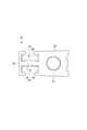
図2に示すようにベースプレート13の基部20に円形のボス孔21が形成されている。ベースプレート13の基部20と前端部22との間に、後述する圧電素子40を収容可能な大きさの一対の開口部23が形成されている。一対の開口部23の間に、ベースプレート13の前後方向(サスペンション10の軸線方向)に延びる帯状の連結部24が設けられている。連結部24は、ベースプレート13の幅方向(図1中に矢印Sで示すスウェイ方向)にある程度撓むことができる。 As shown in FIG. 2, a
ベースプレート13の基部20は、図示しないボイスコイルモータによって駆動されるアクチュエータアームの先端部に固定され、ボイスコイルモータによって旋回駆動されるようになっている。ベースプレート13は板厚が例えば200μm前後のステンレス鋼などの金属板からなる。本実施形態の場合、ベースプレート13とヒンジ部材14とによって、アクチュエータベース25が構成されている。 A
図3に示すようにヒンジ部材14は、ベースプレート13の基部20に重ねて固定される基部30と、ベースプレート13の連結部24と対応した位置に形成された帯状のブリッジ部31と、ベースプレート13の前端部22と対応した位置に形成された中間部32と、板厚方向に弾性変形可能な可撓性を有する一対のヒンジ部33と、ロードビーム11に固定される先端部34などを有している。このヒンジ部材14は、板厚が例えば50μm前後のばね性を有する金属板からなる。 As shown in FIG. 3, the
マイクロアクチュエータ部12には、圧電アクチュエータとして、一対の圧電素子40が搭載されている。圧電素子40はいずれも長方形平板状であり、その長手方向がベースプレート13の前後方向(サスペンション10の軸線方向)に沿って互いにほぼ平行となるように、アクチュエータベース25の開口部23に収容されている。 The
ここで、圧電素子40の構成について、図4および図5を参照しつつ説明する。なお、説明の便宜上、適宜、圧電素子40の長手方向をX方向、短手方向をY方向、厚さ方向をZ方向として説明する。 Here, the configuration of the
圧電素子40は、圧電体41と、圧電体41の対向する一対の主面41a、41b上に配置された一対の電極42A、42Bとで構成されている。圧電素子40の寸法は、一例として、長手方向長さ1.0mm、短手方向長さ0.3mm、厚さ0.05mmである。 The
圧電体41は、長方形平板状であり、たとえばPZT等の圧電材料で構成されている。圧電体41は、その上面41aが正極に、その下面41bが負極になるように分極処理されている。 The
圧電体41の主面(上面41aおよび下面41b)にはそれぞれの中央付近に、識別パターン43A、43Bが形成されている。各識別パターン43A、43Bは、Ag、AgPb合金、Au等の導電材料で構成されている。上面側の識別パターン43Aは、上面42aが正極側であることを示すプラス(+)状パターンであり、一方、下面側の識別パターン43Bは、下面42bが負極側であることを示すマイナス(−)状パターンである。識別パターン43A、43Bの寸法は、一例として、厚さ0.001mm、線幅0.05mmである。
このような識別パターン43A、43Bを有する圧電体41は、一例として、以下のようにして形成することができる。 The
まず、圧電体41となるべき圧電体グリーンシートを準備する。そして、この圧電体グリーンシートの表面に、識別パターンとなるべき導電ペーストを印刷する。そして、圧電体グリーンシートを焼結させ、それと同時に導電ペーストも焼結させる(いわゆる、同時焼成)。それにより、主面41a、41b上に、識別パターン43A、43Bが形成された圧電体41が得られる。この圧電体41においては、その上下面41a、41bは自然面(焼結後の表面状態が維持されている面)である。 First, a piezoelectric green sheet to be the
一対の電極42A、42Bは、圧電体41の主面41a、41bの全域を覆うように設けられている。一対の電極42A、42Bのうち、圧電体41の上面41a側を覆う電極42Aは正極電極であり、一方、圧電体41の下面41b側を覆う電極42Bは負極電極である。各電極42A、42は、Auで構成されており、めっきや蒸着、スパッタ等の真空製膜法によって形成される。このような真空製膜法によれば、焼結に比べて、より緻密な表面状態の電極を形成することができ、パーティクルが生じにくい。 The pair of electrodes 42 </ b> A and 42 </ b> B are provided so as to cover the entire
このような圧電素子40をサスペンション1に搭載するときには、図5に示すように、圧電素子40の長手方向(X方向)が、ベースプレート13の前後方向(サスペンション10の軸線方向)に沿うようにして、ベースプレート13の開口部23に収容する。このとき、圧電素子40の前端部はヒンジ部材14の中間部32に支持されるようにして接着剤50で接着固定され、同様に、圧電素子40の後端部はヒンジ部材14の基部30に支持されるようにして接着剤50で固定される。 When mounting such a
なお、圧電素子40の一対の電極42A、42B間に電圧を印加するために、電極42A、42Bにはそれぞれ図示しない電気配線が設けられる。なお、上述した接着剤50に導電性接着剤を用い、この接着剤50を電気配線の一部として利用してもよい。 In order to apply a voltage between the pair of
一対の圧電素子40をサスペンション10に搭載したときに、一対の圧電素子40に印加する電圧を制御することにより、一方の圧電素子40を長手方向に所定長さだけ伸張させるとともに、他方の圧電素子40を長手方向に所定長さだけ収縮させることができる。このように、サスペンション10においては、一対の圧電素子40の各々の伸縮を制御することで、ロードビーム11側を幅方向(スウェイ方向S)に所望量だけ変位させることができる。 When the pair of
ここで、一対の圧電素子40をサスペンション10に搭載する際には、図1に示すように、それぞれの分極の向きが異なるように、表裏が互いに逆になるように搭載する必要がある。 Here, when the pair of
圧電素子40においては、圧電体41の主面41a、41bのうち、正極に分極された上面41aにプラス状の識別パターン43Aが設けられ、負極に分極された下面41bにマイナス状の識別パターン43Bが設けられているため、圧電素子40の極性をその外観から容易に判別することができる。 In the
その上、各識別パターン43A、43Bは、電極42A、42Bによって完全に覆われているため、各識別パターン43A、43Bから構成材料がパーティクルとして脱離する事態が防止されている。 In addition, since the
以上で説明したとおり、圧電素子40においては、圧電体41の主面41a、41b上に設けられた識別パターン43A、43Bが、電極42A、42Bで覆われていることで、識別パターン43A、43Bに起因するパーティクルの発生が抑制されており、かつ、識別パターン43A、43Bにより圧電素子40の極性をその外観から判別することができる。 As described above, in the
また、圧電素子40においては、各識別パターン43A、43Bが導電材料で構成されている。識別パターンが絶縁材料(圧電材料以外の絶縁材料)で構成されている場合には、識別パターン周辺の圧電体への印加電圧が部分的に低下し、その結果、圧電素子としての機能(上述した伸縮)が低下する虞がある。しかしながら、圧電素子40では、各識別パターン43A、43Bを導電材料で構成しているため、識別パターン43A、43Bが電極42A、42Bの一部として機能し、そのような印加電圧の低下が抑制されている。 In the
なお、本発明は上述した実施形態に限らず、様々な変形が可能である。 The present invention is not limited to the above-described embodiment, and various modifications can be made.
たとえば、識別パターンを、導電材料ではなく圧電材料で構成しても、上述した効果と同様の効果を奏する。このような識別パターンは、圧電体グリーンシートの表面に、上述した導電ペーストの代わりに圧電体ペースト(たとえばPZTペースト)を印刷して焼成することで得ることができる。この場合、識別パターンが圧電体の一部として機能するため、識別パターンが導電材料で構成されている場合と同様に、上述した印加電圧の低下が抑制される。なお、識別パターンを構成する圧電材料は、圧電体41と同じ組成の圧電材料(たとえばPZT)であることが好ましい。 For example, even if the identification pattern is made of a piezoelectric material instead of a conductive material, the same effect as described above can be obtained. Such an identification pattern can be obtained by printing and baking a piezoelectric paste (for example, PZT paste) on the surface of the piezoelectric green sheet instead of the conductive paste described above. In this case, since the identification pattern functions as a part of the piezoelectric body, the above-described decrease in applied voltage is suppressed as in the case where the identification pattern is made of a conductive material. Note that the piezoelectric material constituting the identification pattern is preferably a piezoelectric material (for example, PZT) having the same composition as the
また、識別パターンの形状は、互いに異なる形状であれば、プラス形状やマイナス形状に限らず、その他の形状に適宜変更可能である。また、識別パターンは、必ずしも圧電体の上下面の両方に設ける必要はなく、上下面の一方にのみ設けてもよい。さらに、識別パターンは、識別性を有するその他の形状や文字、模様等であってもよい。 Further, the shape of the identification pattern is not limited to the plus shape and the minus shape as long as the shapes are different from each other, and can be appropriately changed to other shapes. The identification pattern is not necessarily provided on both the upper and lower surfaces of the piezoelectric body, and may be provided only on one of the upper and lower surfaces. Further, the identification pattern may be other shapes, characters, patterns or the like having identification.
また、圧電体は、単層の圧電体に限らず、圧電層と内部電極層とが交互に積層された圧電積層体であってもよい。圧電体が圧電積層体である場合、応力の低減等の観点から、識別パターンの構成材料を内部電極層の構成材料と同じにすることが好ましい。 The piezoelectric body is not limited to a single-layer piezoelectric body, and may be a piezoelectric laminated body in which piezoelectric layers and internal electrode layers are alternately laminated. When the piezoelectric body is a piezoelectric laminated body, it is preferable that the constituent material of the identification pattern is the same as the constituent material of the internal electrode layer from the viewpoint of reducing stress.
電極は、必ずしも識別パターンを全体的に覆う必要はなく、識別パターンの一部分が電極から露出していても構わない。この場合でも、電極に覆われた箇所においては識別パターンからのパーティクルの発生が抑制される。また、電極は、必ずしも圧電体の主面の全域を覆うように設ける必要はなく、主面の一部に設けるようにしてもよい。 The electrode does not necessarily need to cover the entire identification pattern, and a part of the identification pattern may be exposed from the electrode. Even in this case, the generation of particles from the identification pattern is suppressed at the portion covered with the electrode. Further, the electrode is not necessarily provided so as to cover the entire main surface of the piezoelectric body, and may be provided on a part of the main surface.
10…サスペンション、40…圧電素子、41…圧電体、42A、42B…電極、43A、43B…識別パターン。
DESCRIPTION OF
Claims (4)
Translated fromJapanese前記圧電体の主面上に配置された電極と、
前記圧電体の主面から突出するように設けられ、導電材料で構成されるとともに前記電極で覆われた識別パターンと
を備える圧電素子。A piezoelectric body having a pair of main surfaces facing each other;
An electrode disposed on the main surface of the piezoelectric body;
A piezoelectric element provided with an identification pattern which is providedso asto protrude from the main surface of the piezoelectric body and is made of aconductive material and coveredwith the electrode.
前記圧電体の主面上に配置された電極と、
前記圧電体の主面から突出するように設けられ、圧電材料で構成されるとともに前記電極で覆われた識別パターンと
を備える圧電素子。A piezoelectric body having a pair of main surfaces facing each other;
An electrode disposed on the main surface of the piezoelectric body;
A piezoelectric element provided with an identification pattern providedso asto protrude from the main surface of the piezoelectric body and made of apiezoelectric material and coveredwith the electrode.
前記圧電体の主面上に配置された電極と、
前記圧電体の主面から突出するように設けられ、絶縁材料で構成されるとともに前記電極で覆われた識別パターンと
を備える圧電素子。A piezoelectric body having a pair of main surfaces facing each other;
An electrode disposed on the main surface of the piezoelectric body;
A piezoelectric element provided with an identification pattern which is providedso asto protrude from the main surface of the piezoelectric body and is made of aninsulating material and coveredwith the electrode.
一方の前記主面に設けられた前記識別パターンの形状と、他方の前記主面に形成された前記識別パターンの形状とが異なる、請求項1〜3のいずれか一項に記載の圧電素子。The piezoelectric element according to any one of claims 1 to 3, wherein a shape of the identification pattern provided on one main surface is different from a shape of the identification pattern formed on the other main surface.
Priority Applications (2)
| Application Number | Priority Date | Filing Date | Title |
|---|---|---|---|
| JP2013092888AJP5633599B2 (en) | 2013-04-25 | 2013-04-25 | Piezoelectric element |
| US14/182,589US9755134B2 (en) | 2013-04-25 | 2014-02-18 | Piezoelectric device |
Applications Claiming Priority (1)
| Application Number | Priority Date | Filing Date | Title |
|---|---|---|---|
| JP2013092888AJP5633599B2 (en) | 2013-04-25 | 2013-04-25 | Piezoelectric element |
Publications (2)
| Publication Number | Publication Date |
|---|---|
| JP2014216494A JP2014216494A (en) | 2014-11-17 |
| JP5633599B2true JP5633599B2 (en) | 2014-12-03 |
Family
ID=51788676
Family Applications (1)
| Application Number | Title | Priority Date | Filing Date |
|---|---|---|---|
| JP2013092888AActiveJP5633599B2 (en) | 2013-04-25 | 2013-04-25 | Piezoelectric element |
Country Status (2)
| Country | Link |
|---|---|
| US (1) | US9755134B2 (en) |
| JP (1) | JP5633599B2 (en) |
Families Citing this family (4)
| Publication number | Priority date | Publication date | Assignee | Title |
|---|---|---|---|---|
| DE202016102203U1 (en)* | 2016-04-26 | 2016-06-29 | Epcos Ag | Multilayer component |
| USD857020S1 (en)* | 2016-05-25 | 2019-08-20 | Tdk Corporation | Piezoelectric element |
| JP1565481S (en)* | 2016-05-25 | 2016-12-19 | ||
| JP1649916S (en)* | 2019-05-20 | 2020-01-20 |
Family Cites Families (8)
| Publication number | Priority date | Publication date | Assignee | Title |
|---|---|---|---|---|
| JP2002203999A (en)* | 2000-11-06 | 2002-07-19 | Denso Corp | Laminated type piezoelectric-substance element and the manufacturing method thereof |
| JP2002190457A (en) | 2000-12-20 | 2002-07-05 | Fdk Corp | Method of manufacturing and handling element with directionality |
| JP4237394B2 (en)* | 2000-12-27 | 2009-03-11 | 日本発條株式会社 | Suspension for disk unit |
| JP2002229271A (en)* | 2001-02-05 | 2002-08-14 | Canon Inc | Image forming method |
| JP4664700B2 (en)* | 2005-02-15 | 2011-04-06 | シチズンホールディングス株式会社 | Method for manufacturing vibrator device |
| JP5083710B2 (en)* | 2006-09-19 | 2012-11-28 | セイコーエプソン株式会社 | Piezoelectric device and method for manufacturing piezoelectric device |
| JP5262573B2 (en)* | 2008-10-24 | 2013-08-14 | 株式会社村田製作所 | Method for manufacturing acoustic wave device |
| JP5500872B2 (en)* | 2009-05-29 | 2014-05-21 | 日本発條株式会社 | Piezoelectric element with electrode and head suspension |
- 2013
- 2013-04-25JPJP2013092888Apatent/JP5633599B2/enactiveActive
- 2014
- 2014-02-18USUS14/182,589patent/US9755134B2/enactiveActive
Also Published As
| Publication number | Publication date |
|---|---|
| US9755134B2 (en) | 2017-09-05 |
| JP2014216494A (en) | 2014-11-17 |
| US20140319973A1 (en) | 2014-10-30 |
Similar Documents
| Publication | Publication Date | Title |
|---|---|---|
| JP5943658B2 (en) | Terminal structure, flexure, and head suspension | |
| JP5440697B2 (en) | Piezoelectric actuator and drive device | |
| JP5633599B2 (en) | Piezoelectric element | |
| CN102044262B (en) | Magnetic head driving piezoelectric ceramic actuator | |
| JP6629587B2 (en) | Suspension structure | |
| JP5500872B2 (en) | Piezoelectric element with electrode and head suspension | |
| JP5941332B2 (en) | Head suspension | |
| JP2013211078A (en) | Terminal part, flexure and head suspension | |
| JP6536269B2 (en) | Piezoelectric element and piezoelectric actuator | |
| JP5463824B2 (en) | Flexure, suspension, suspension with head, hard disk drive, and method of manufacturing flexure | |
| JP6361640B2 (en) | Piezoelectric element and piezoelectric actuator | |
| JP6439422B6 (en) | Piezoelectric actuator | |
| JP2002345265A (en) | Piezo actuator | |
| JP6103689B2 (en) | Dielectric element | |
| JP4915435B2 (en) | Piezoelectric actuator | |
| JP5633549B2 (en) | Piezoelectric element | |
| JP5804359B2 (en) | Suspension, suspension with head and hard disk drive | |
| JP5713133B1 (en) | Piezoelectric actuator | |
| JP6439438B6 (en) | Piezoelectric actuator | |
| JP6841077B2 (en) | Acceleration sensor | |
| WO2016076361A1 (en) | Piezoelectric device | |
| JP2015008300A (en) | Lens driving device | |
| JP2014078624A (en) | Piezoelectric element | |
| JP2007142209A (en) | Piezoelectric element and manufacturing method thereof | |
| JP2017188602A (en) | Piezoelectric actuator |
Legal Events
| Date | Code | Title | Description |
|---|---|---|---|
| TRDD | Decision of grant or rejection written | ||
| A01 | Written decision to grant a patent or to grant a registration (utility model) | Free format text:JAPANESE INTERMEDIATE CODE: A01 Effective date:20140916 | |
| A61 | First payment of annual fees (during grant procedure) | Free format text:JAPANESE INTERMEDIATE CODE: A61 Effective date:20140929 | |
| R150 | Certificate of patent or registration of utility model | Ref document number:5633599 Country of ref document:JP Free format text:JAPANESE INTERMEDIATE CODE: R150 | |
| R250 | Receipt of annual fees | Free format text:JAPANESE INTERMEDIATE CODE: R250 | |
| R250 | Receipt of annual fees | Free format text:JAPANESE INTERMEDIATE CODE: R250 |