JP5629580B2 - Flip chip interconnect with double posts - Google Patents
Flip chip interconnect with double postsDownload PDFInfo
- Publication number
- JP5629580B2 JP5629580B2JP2010526972AJP2010526972AJP5629580B2JP 5629580 B2JP5629580 B2JP 5629580B2JP 2010526972 AJP2010526972 AJP 2010526972AJP 2010526972 AJP2010526972 AJP 2010526972AJP 5629580 B2JP5629580 B2JP 5629580B2
- Authority
- JP
- Japan
- Prior art keywords
- post
- substrate
- microelectronic element
- metal
- posts
- Prior art date
- Legal status (The legal status is an assumption and is not a legal conclusion. Google has not performed a legal analysis and makes no representation as to the accuracy of the status listed.)
- Active
Links
Images


Classifications
- H—ELECTRICITY
- H01—ELECTRIC ELEMENTS
- H01L—SEMICONDUCTOR DEVICES NOT COVERED BY CLASS H10
- H01L24/00—Arrangements for connecting or disconnecting semiconductor or solid-state bodies; Methods or apparatus related thereto
- H01L24/01—Means for bonding being attached to, or being formed on, the surface to be connected, e.g. chip-to-package, die-attach, "first-level" interconnects; Manufacturing methods related thereto
- H01L24/10—Bump connectors ; Manufacturing methods related thereto
- H01L24/12—Structure, shape, material or disposition of the bump connectors prior to the connecting process
- H01L24/14—Structure, shape, material or disposition of the bump connectors prior to the connecting process of a plurality of bump connectors
- H—ELECTRICITY
- H01—ELECTRIC ELEMENTS
- H01L—SEMICONDUCTOR DEVICES NOT COVERED BY CLASS H10
- H01L21/00—Processes or apparatus adapted for the manufacture or treatment of semiconductor or solid state devices or of parts thereof
- H01L21/02—Manufacture or treatment of semiconductor devices or of parts thereof
- H01L21/04—Manufacture or treatment of semiconductor devices or of parts thereof the devices having potential barriers, e.g. a PN junction, depletion layer or carrier concentration layer
- H01L21/48—Manufacture or treatment of parts, e.g. containers, prior to assembly of the devices, using processes not provided for in a single one of the groups H01L21/18 - H01L21/326 or H10D48/04 - H10D48/07
- H01L21/4814—Conductive parts
- H01L21/4846—Leads on or in insulating or insulated substrates, e.g. metallisation
- H01L21/4853—Connection or disconnection of other leads to or from a metallisation, e.g. pins, wires, bumps
- H—ELECTRICITY
- H01—ELECTRIC ELEMENTS
- H01L—SEMICONDUCTOR DEVICES NOT COVERED BY CLASS H10
- H01L23/00—Details of semiconductor or other solid state devices
- H01L23/28—Encapsulations, e.g. encapsulating layers, coatings, e.g. for protection
- H01L23/31—Encapsulations, e.g. encapsulating layers, coatings, e.g. for protection characterised by the arrangement or shape
- H01L23/3157—Partial encapsulation or coating
- H01L23/3178—Coating or filling in grooves made in the semiconductor body
- H—ELECTRICITY
- H01—ELECTRIC ELEMENTS
- H01L—SEMICONDUCTOR DEVICES NOT COVERED BY CLASS H10
- H01L23/00—Details of semiconductor or other solid state devices
- H01L23/48—Arrangements for conducting electric current to or from the solid state body in operation, e.g. leads, terminal arrangements ; Selection of materials therefor
- H01L23/488—Arrangements for conducting electric current to or from the solid state body in operation, e.g. leads, terminal arrangements ; Selection of materials therefor consisting of soldered or bonded constructions
- H01L23/498—Leads, i.e. metallisations or lead-frames on insulating substrates, e.g. chip carriers
- H01L23/49811—Additional leads joined to the metallisation on the insulating substrate, e.g. pins, bumps, wires, flat leads
- H01L23/49816—Spherical bumps on the substrate for external connection, e.g. ball grid arrays [BGA]
- H—ELECTRICITY
- H01—ELECTRIC ELEMENTS
- H01L—SEMICONDUCTOR DEVICES NOT COVERED BY CLASS H10
- H01L24/00—Arrangements for connecting or disconnecting semiconductor or solid-state bodies; Methods or apparatus related thereto
- H01L24/01—Means for bonding being attached to, or being formed on, the surface to be connected, e.g. chip-to-package, die-attach, "first-level" interconnects; Manufacturing methods related thereto
- H01L24/10—Bump connectors ; Manufacturing methods related thereto
- H01L24/11—Manufacturing methods
- H—ELECTRICITY
- H01—ELECTRIC ELEMENTS
- H01L—SEMICONDUCTOR DEVICES NOT COVERED BY CLASS H10
- H01L24/00—Arrangements for connecting or disconnecting semiconductor or solid-state bodies; Methods or apparatus related thereto
- H01L24/01—Means for bonding being attached to, or being formed on, the surface to be connected, e.g. chip-to-package, die-attach, "first-level" interconnects; Manufacturing methods related thereto
- H01L24/10—Bump connectors ; Manufacturing methods related thereto
- H01L24/12—Structure, shape, material or disposition of the bump connectors prior to the connecting process
- H01L24/13—Structure, shape, material or disposition of the bump connectors prior to the connecting process of an individual bump connector
- H—ELECTRICITY
- H01—ELECTRIC ELEMENTS
- H01L—SEMICONDUCTOR DEVICES NOT COVERED BY CLASS H10
- H01L24/00—Arrangements for connecting or disconnecting semiconductor or solid-state bodies; Methods or apparatus related thereto
- H01L24/01—Means for bonding being attached to, or being formed on, the surface to be connected, e.g. chip-to-package, die-attach, "first-level" interconnects; Manufacturing methods related thereto
- H01L24/10—Bump connectors ; Manufacturing methods related thereto
- H01L24/15—Structure, shape, material or disposition of the bump connectors after the connecting process
- H01L24/16—Structure, shape, material or disposition of the bump connectors after the connecting process of an individual bump connector
- H—ELECTRICITY
- H01—ELECTRIC ELEMENTS
- H01L—SEMICONDUCTOR DEVICES NOT COVERED BY CLASS H10
- H01L24/00—Arrangements for connecting or disconnecting semiconductor or solid-state bodies; Methods or apparatus related thereto
- H01L24/80—Methods for connecting semiconductor or other solid state bodies using means for bonding being attached to, or being formed on, the surface to be connected
- H01L24/81—Methods for connecting semiconductor or other solid state bodies using means for bonding being attached to, or being formed on, the surface to be connected using a bump connector
- H—ELECTRICITY
- H01—ELECTRIC ELEMENTS
- H01L—SEMICONDUCTOR DEVICES NOT COVERED BY CLASS H10
- H01L25/00—Assemblies consisting of a plurality of semiconductor or other solid state devices
- H01L25/03—Assemblies consisting of a plurality of semiconductor or other solid state devices all the devices being of a type provided for in a single subclass of subclasses H10B, H10D, H10F, H10H, H10K or H10N, e.g. assemblies of rectifier diodes
- H01L25/04—Assemblies consisting of a plurality of semiconductor or other solid state devices all the devices being of a type provided for in a single subclass of subclasses H10B, H10D, H10F, H10H, H10K or H10N, e.g. assemblies of rectifier diodes the devices not having separate containers
- H01L25/065—Assemblies consisting of a plurality of semiconductor or other solid state devices all the devices being of a type provided for in a single subclass of subclasses H10B, H10D, H10F, H10H, H10K or H10N, e.g. assemblies of rectifier diodes the devices not having separate containers the devices being of a type provided for in group H10D89/00
- H01L25/0657—Stacked arrangements of devices
- H—ELECTRICITY
- H01—ELECTRIC ELEMENTS
- H01L—SEMICONDUCTOR DEVICES NOT COVERED BY CLASS H10
- H01L25/00—Assemblies consisting of a plurality of semiconductor or other solid state devices
- H01L25/03—Assemblies consisting of a plurality of semiconductor or other solid state devices all the devices being of a type provided for in a single subclass of subclasses H10B, H10D, H10F, H10H, H10K or H10N, e.g. assemblies of rectifier diodes
- H01L25/10—Assemblies consisting of a plurality of semiconductor or other solid state devices all the devices being of a type provided for in a single subclass of subclasses H10B, H10D, H10F, H10H, H10K or H10N, e.g. assemblies of rectifier diodes the devices having separate containers
- H01L25/105—Assemblies consisting of a plurality of semiconductor or other solid state devices all the devices being of a type provided for in a single subclass of subclasses H10B, H10D, H10F, H10H, H10K or H10N, e.g. assemblies of rectifier diodes the devices having separate containers the devices being integrated devices of class H10
- H—ELECTRICITY
- H01—ELECTRIC ELEMENTS
- H01L—SEMICONDUCTOR DEVICES NOT COVERED BY CLASS H10
- H01L21/00—Processes or apparatus adapted for the manufacture or treatment of semiconductor or solid state devices or of parts thereof
- H01L21/02—Manufacture or treatment of semiconductor devices or of parts thereof
- H01L21/04—Manufacture or treatment of semiconductor devices or of parts thereof the devices having potential barriers, e.g. a PN junction, depletion layer or carrier concentration layer
- H01L21/50—Assembly of semiconductor devices using processes or apparatus not provided for in a single one of the groups H01L21/18 - H01L21/326 or H10D48/04 - H10D48/07 e.g. sealing of a cap to a base of a container
- H01L21/56—Encapsulations, e.g. encapsulation layers, coatings
- H01L21/563—Encapsulation of active face of flip-chip device, e.g. underfilling or underencapsulation of flip-chip, encapsulation preform on chip or mounting substrate
- H—ELECTRICITY
- H01—ELECTRIC ELEMENTS
- H01L—SEMICONDUCTOR DEVICES NOT COVERED BY CLASS H10
- H01L2224/00—Indexing scheme for arrangements for connecting or disconnecting semiconductor or solid-state bodies and methods related thereto as covered by H01L24/00
- H01L2224/01—Means for bonding being attached to, or being formed on, the surface to be connected, e.g. chip-to-package, die-attach, "first-level" interconnects; Manufacturing methods related thereto
- H01L2224/02—Bonding areas; Manufacturing methods related thereto
- H01L2224/04—Structure, shape, material or disposition of the bonding areas prior to the connecting process
- H01L2224/0401—Bonding areas specifically adapted for bump connectors, e.g. under bump metallisation [UBM]
- H—ELECTRICITY
- H01—ELECTRIC ELEMENTS
- H01L—SEMICONDUCTOR DEVICES NOT COVERED BY CLASS H10
- H01L2224/00—Indexing scheme for arrangements for connecting or disconnecting semiconductor or solid-state bodies and methods related thereto as covered by H01L24/00
- H01L2224/01—Means for bonding being attached to, or being formed on, the surface to be connected, e.g. chip-to-package, die-attach, "first-level" interconnects; Manufacturing methods related thereto
- H01L2224/02—Bonding areas; Manufacturing methods related thereto
- H01L2224/04—Structure, shape, material or disposition of the bonding areas prior to the connecting process
- H01L2224/05—Structure, shape, material or disposition of the bonding areas prior to the connecting process of an individual bonding area
- H01L2224/0554—External layer
- H01L2224/05575—Plural external layers
- H01L2224/0558—Plural external layers being stacked
- H—ELECTRICITY
- H01—ELECTRIC ELEMENTS
- H01L—SEMICONDUCTOR DEVICES NOT COVERED BY CLASS H10
- H01L2224/00—Indexing scheme for arrangements for connecting or disconnecting semiconductor or solid-state bodies and methods related thereto as covered by H01L24/00
- H01L2224/01—Means for bonding being attached to, or being formed on, the surface to be connected, e.g. chip-to-package, die-attach, "first-level" interconnects; Manufacturing methods related thereto
- H01L2224/02—Bonding areas; Manufacturing methods related thereto
- H01L2224/04—Structure, shape, material or disposition of the bonding areas prior to the connecting process
- H01L2224/05—Structure, shape, material or disposition of the bonding areas prior to the connecting process of an individual bonding area
- H01L2224/0554—External layer
- H01L2224/05599—Material
- H01L2224/056—Material with a principal constituent of the material being a metal or a metalloid, e.g. boron [B], silicon [Si], germanium [Ge], arsenic [As], antimony [Sb], tellurium [Te] and polonium [Po], and alloys thereof
- H01L2224/05617—Material with a principal constituent of the material being a metal or a metalloid, e.g. boron [B], silicon [Si], germanium [Ge], arsenic [As], antimony [Sb], tellurium [Te] and polonium [Po], and alloys thereof the principal constituent melting at a temperature of greater than or equal to 400°C and less than 950°C
- H01L2224/05624—Aluminium [Al] as principal constituent
- H—ELECTRICITY
- H01—ELECTRIC ELEMENTS
- H01L—SEMICONDUCTOR DEVICES NOT COVERED BY CLASS H10
- H01L2224/00—Indexing scheme for arrangements for connecting or disconnecting semiconductor or solid-state bodies and methods related thereto as covered by H01L24/00
- H01L2224/01—Means for bonding being attached to, or being formed on, the surface to be connected, e.g. chip-to-package, die-attach, "first-level" interconnects; Manufacturing methods related thereto
- H01L2224/02—Bonding areas; Manufacturing methods related thereto
- H01L2224/04—Structure, shape, material or disposition of the bonding areas prior to the connecting process
- H01L2224/05—Structure, shape, material or disposition of the bonding areas prior to the connecting process of an individual bonding area
- H01L2224/0554—External layer
- H01L2224/05599—Material
- H01L2224/056—Material with a principal constituent of the material being a metal or a metalloid, e.g. boron [B], silicon [Si], germanium [Ge], arsenic [As], antimony [Sb], tellurium [Te] and polonium [Po], and alloys thereof
- H01L2224/05638—Material with a principal constituent of the material being a metal or a metalloid, e.g. boron [B], silicon [Si], germanium [Ge], arsenic [As], antimony [Sb], tellurium [Te] and polonium [Po], and alloys thereof the principal constituent melting at a temperature of greater than or equal to 950°C and less than 1550°C
- H01L2224/05644—Gold [Au] as principal constituent
- H—ELECTRICITY
- H01—ELECTRIC ELEMENTS
- H01L—SEMICONDUCTOR DEVICES NOT COVERED BY CLASS H10
- H01L2224/00—Indexing scheme for arrangements for connecting or disconnecting semiconductor or solid-state bodies and methods related thereto as covered by H01L24/00
- H01L2224/01—Means for bonding being attached to, or being formed on, the surface to be connected, e.g. chip-to-package, die-attach, "first-level" interconnects; Manufacturing methods related thereto
- H01L2224/10—Bump connectors; Manufacturing methods related thereto
- H01L2224/11—Manufacturing methods
- H01L2224/1147—Manufacturing methods using a lift-off mask
- H—ELECTRICITY
- H01—ELECTRIC ELEMENTS
- H01L—SEMICONDUCTOR DEVICES NOT COVERED BY CLASS H10
- H01L2224/00—Indexing scheme for arrangements for connecting or disconnecting semiconductor or solid-state bodies and methods related thereto as covered by H01L24/00
- H01L2224/01—Means for bonding being attached to, or being formed on, the surface to be connected, e.g. chip-to-package, die-attach, "first-level" interconnects; Manufacturing methods related thereto
- H01L2224/10—Bump connectors; Manufacturing methods related thereto
- H01L2224/12—Structure, shape, material or disposition of the bump connectors prior to the connecting process
- H01L2224/13—Structure, shape, material or disposition of the bump connectors prior to the connecting process of an individual bump connector
- H01L2224/13001—Core members of the bump connector
- H01L2224/1301—Shape
- H01L2224/13012—Shape in top view
- H01L2224/13015—Shape in top view comprising protrusions or indentations
- H—ELECTRICITY
- H01—ELECTRIC ELEMENTS
- H01L—SEMICONDUCTOR DEVICES NOT COVERED BY CLASS H10
- H01L2224/00—Indexing scheme for arrangements for connecting or disconnecting semiconductor or solid-state bodies and methods related thereto as covered by H01L24/00
- H01L2224/01—Means for bonding being attached to, or being formed on, the surface to be connected, e.g. chip-to-package, die-attach, "first-level" interconnects; Manufacturing methods related thereto
- H01L2224/10—Bump connectors; Manufacturing methods related thereto
- H01L2224/12—Structure, shape, material or disposition of the bump connectors prior to the connecting process
- H01L2224/13—Structure, shape, material or disposition of the bump connectors prior to the connecting process of an individual bump connector
- H01L2224/13001—Core members of the bump connector
- H01L2224/1301—Shape
- H01L2224/13016—Shape in side view
- H01L2224/13017—Shape in side view being non uniform along the bump connector
- H—ELECTRICITY
- H01—ELECTRIC ELEMENTS
- H01L—SEMICONDUCTOR DEVICES NOT COVERED BY CLASS H10
- H01L2224/00—Indexing scheme for arrangements for connecting or disconnecting semiconductor or solid-state bodies and methods related thereto as covered by H01L24/00
- H01L2224/01—Means for bonding being attached to, or being formed on, the surface to be connected, e.g. chip-to-package, die-attach, "first-level" interconnects; Manufacturing methods related thereto
- H01L2224/10—Bump connectors; Manufacturing methods related thereto
- H01L2224/12—Structure, shape, material or disposition of the bump connectors prior to the connecting process
- H01L2224/13—Structure, shape, material or disposition of the bump connectors prior to the connecting process of an individual bump connector
- H01L2224/13001—Core members of the bump connector
- H01L2224/1301—Shape
- H01L2224/13016—Shape in side view
- H01L2224/13018—Shape in side view comprising protrusions or indentations
- H01L2224/13019—Shape in side view comprising protrusions or indentations at the bonding interface of the bump connector, i.e. on the surface of the bump connector
- H—ELECTRICITY
- H01—ELECTRIC ELEMENTS
- H01L—SEMICONDUCTOR DEVICES NOT COVERED BY CLASS H10
- H01L2224/00—Indexing scheme for arrangements for connecting or disconnecting semiconductor or solid-state bodies and methods related thereto as covered by H01L24/00
- H01L2224/01—Means for bonding being attached to, or being formed on, the surface to be connected, e.g. chip-to-package, die-attach, "first-level" interconnects; Manufacturing methods related thereto
- H01L2224/10—Bump connectors; Manufacturing methods related thereto
- H01L2224/12—Structure, shape, material or disposition of the bump connectors prior to the connecting process
- H01L2224/13—Structure, shape, material or disposition of the bump connectors prior to the connecting process of an individual bump connector
- H01L2224/13001—Core members of the bump connector
- H01L2224/1302—Disposition
- H01L2224/13023—Disposition the whole bump connector protruding from the surface
- H—ELECTRICITY
- H01—ELECTRIC ELEMENTS
- H01L—SEMICONDUCTOR DEVICES NOT COVERED BY CLASS H10
- H01L2224/00—Indexing scheme for arrangements for connecting or disconnecting semiconductor or solid-state bodies and methods related thereto as covered by H01L24/00
- H01L2224/01—Means for bonding being attached to, or being formed on, the surface to be connected, e.g. chip-to-package, die-attach, "first-level" interconnects; Manufacturing methods related thereto
- H01L2224/10—Bump connectors; Manufacturing methods related thereto
- H01L2224/12—Structure, shape, material or disposition of the bump connectors prior to the connecting process
- H01L2224/13—Structure, shape, material or disposition of the bump connectors prior to the connecting process of an individual bump connector
- H01L2224/13001—Core members of the bump connector
- H01L2224/13075—Plural core members
- H01L2224/1308—Plural core members being stacked
- H01L2224/13082—Two-layer arrangements
- H—ELECTRICITY
- H01—ELECTRIC ELEMENTS
- H01L—SEMICONDUCTOR DEVICES NOT COVERED BY CLASS H10
- H01L2224/00—Indexing scheme for arrangements for connecting or disconnecting semiconductor or solid-state bodies and methods related thereto as covered by H01L24/00
- H01L2224/01—Means for bonding being attached to, or being formed on, the surface to be connected, e.g. chip-to-package, die-attach, "first-level" interconnects; Manufacturing methods related thereto
- H01L2224/10—Bump connectors; Manufacturing methods related thereto
- H01L2224/12—Structure, shape, material or disposition of the bump connectors prior to the connecting process
- H01L2224/13—Structure, shape, material or disposition of the bump connectors prior to the connecting process of an individual bump connector
- H01L2224/13001—Core members of the bump connector
- H01L2224/13099—Material
- H01L2224/131—Material with a principal constituent of the material being a metal or a metalloid, e.g. boron [B], silicon [Si], germanium [Ge], arsenic [As], antimony [Sb], tellurium [Te] and polonium [Po], and alloys thereof
- H01L2224/13101—Material with a principal constituent of the material being a metal or a metalloid, e.g. boron [B], silicon [Si], germanium [Ge], arsenic [As], antimony [Sb], tellurium [Te] and polonium [Po], and alloys thereof the principal constituent melting at a temperature of less than 400°C
- H01L2224/13111—Tin [Sn] as principal constituent
- H—ELECTRICITY
- H01—ELECTRIC ELEMENTS
- H01L—SEMICONDUCTOR DEVICES NOT COVERED BY CLASS H10
- H01L2224/00—Indexing scheme for arrangements for connecting or disconnecting semiconductor or solid-state bodies and methods related thereto as covered by H01L24/00
- H01L2224/01—Means for bonding being attached to, or being formed on, the surface to be connected, e.g. chip-to-package, die-attach, "first-level" interconnects; Manufacturing methods related thereto
- H01L2224/10—Bump connectors; Manufacturing methods related thereto
- H01L2224/12—Structure, shape, material or disposition of the bump connectors prior to the connecting process
- H01L2224/13—Structure, shape, material or disposition of the bump connectors prior to the connecting process of an individual bump connector
- H01L2224/13001—Core members of the bump connector
- H01L2224/13099—Material
- H01L2224/131—Material with a principal constituent of the material being a metal or a metalloid, e.g. boron [B], silicon [Si], germanium [Ge], arsenic [As], antimony [Sb], tellurium [Te] and polonium [Po], and alloys thereof
- H01L2224/13117—Material with a principal constituent of the material being a metal or a metalloid, e.g. boron [B], silicon [Si], germanium [Ge], arsenic [As], antimony [Sb], tellurium [Te] and polonium [Po], and alloys thereof the principal constituent melting at a temperature of greater than or equal to 400°C and less than 950°C
- H01L2224/13124—Aluminium [Al] as principal constituent
- H—ELECTRICITY
- H01—ELECTRIC ELEMENTS
- H01L—SEMICONDUCTOR DEVICES NOT COVERED BY CLASS H10
- H01L2224/00—Indexing scheme for arrangements for connecting or disconnecting semiconductor or solid-state bodies and methods related thereto as covered by H01L24/00
- H01L2224/01—Means for bonding being attached to, or being formed on, the surface to be connected, e.g. chip-to-package, die-attach, "first-level" interconnects; Manufacturing methods related thereto
- H01L2224/10—Bump connectors; Manufacturing methods related thereto
- H01L2224/12—Structure, shape, material or disposition of the bump connectors prior to the connecting process
- H01L2224/13—Structure, shape, material or disposition of the bump connectors prior to the connecting process of an individual bump connector
- H01L2224/13001—Core members of the bump connector
- H01L2224/13099—Material
- H01L2224/131—Material with a principal constituent of the material being a metal or a metalloid, e.g. boron [B], silicon [Si], germanium [Ge], arsenic [As], antimony [Sb], tellurium [Te] and polonium [Po], and alloys thereof
- H01L2224/13138—Material with a principal constituent of the material being a metal or a metalloid, e.g. boron [B], silicon [Si], germanium [Ge], arsenic [As], antimony [Sb], tellurium [Te] and polonium [Po], and alloys thereof the principal constituent melting at a temperature of greater than or equal to 950°C and less than 1550°C
- H01L2224/13144—Gold [Au] as principal constituent
- H—ELECTRICITY
- H01—ELECTRIC ELEMENTS
- H01L—SEMICONDUCTOR DEVICES NOT COVERED BY CLASS H10
- H01L2224/00—Indexing scheme for arrangements for connecting or disconnecting semiconductor or solid-state bodies and methods related thereto as covered by H01L24/00
- H01L2224/01—Means for bonding being attached to, or being formed on, the surface to be connected, e.g. chip-to-package, die-attach, "first-level" interconnects; Manufacturing methods related thereto
- H01L2224/10—Bump connectors; Manufacturing methods related thereto
- H01L2224/12—Structure, shape, material or disposition of the bump connectors prior to the connecting process
- H01L2224/13—Structure, shape, material or disposition of the bump connectors prior to the connecting process of an individual bump connector
- H01L2224/13001—Core members of the bump connector
- H01L2224/13099—Material
- H01L2224/131—Material with a principal constituent of the material being a metal or a metalloid, e.g. boron [B], silicon [Si], germanium [Ge], arsenic [As], antimony [Sb], tellurium [Te] and polonium [Po], and alloys thereof
- H01L2224/13138—Material with a principal constituent of the material being a metal or a metalloid, e.g. boron [B], silicon [Si], germanium [Ge], arsenic [As], antimony [Sb], tellurium [Te] and polonium [Po], and alloys thereof the principal constituent melting at a temperature of greater than or equal to 950°C and less than 1550°C
- H01L2224/13147—Copper [Cu] as principal constituent
- H—ELECTRICITY
- H01—ELECTRIC ELEMENTS
- H01L—SEMICONDUCTOR DEVICES NOT COVERED BY CLASS H10
- H01L2224/00—Indexing scheme for arrangements for connecting or disconnecting semiconductor or solid-state bodies and methods related thereto as covered by H01L24/00
- H01L2224/01—Means for bonding being attached to, or being formed on, the surface to be connected, e.g. chip-to-package, die-attach, "first-level" interconnects; Manufacturing methods related thereto
- H01L2224/10—Bump connectors; Manufacturing methods related thereto
- H01L2224/12—Structure, shape, material or disposition of the bump connectors prior to the connecting process
- H01L2224/13—Structure, shape, material or disposition of the bump connectors prior to the connecting process of an individual bump connector
- H01L2224/13001—Core members of the bump connector
- H01L2224/13099—Material
- H01L2224/131—Material with a principal constituent of the material being a metal or a metalloid, e.g. boron [B], silicon [Si], germanium [Ge], arsenic [As], antimony [Sb], tellurium [Te] and polonium [Po], and alloys thereof
- H01L2224/13138—Material with a principal constituent of the material being a metal or a metalloid, e.g. boron [B], silicon [Si], germanium [Ge], arsenic [As], antimony [Sb], tellurium [Te] and polonium [Po], and alloys thereof the principal constituent melting at a temperature of greater than or equal to 950°C and less than 1550°C
- H01L2224/13155—Nickel [Ni] as principal constituent
- H—ELECTRICITY
- H01—ELECTRIC ELEMENTS
- H01L—SEMICONDUCTOR DEVICES NOT COVERED BY CLASS H10
- H01L2224/00—Indexing scheme for arrangements for connecting or disconnecting semiconductor or solid-state bodies and methods related thereto as covered by H01L24/00
- H01L2224/01—Means for bonding being attached to, or being formed on, the surface to be connected, e.g. chip-to-package, die-attach, "first-level" interconnects; Manufacturing methods related thereto
- H01L2224/10—Bump connectors; Manufacturing methods related thereto
- H01L2224/12—Structure, shape, material or disposition of the bump connectors prior to the connecting process
- H01L2224/14—Structure, shape, material or disposition of the bump connectors prior to the connecting process of a plurality of bump connectors
- H01L2224/141—Disposition
- H01L2224/1412—Layout
- H—ELECTRICITY
- H01—ELECTRIC ELEMENTS
- H01L—SEMICONDUCTOR DEVICES NOT COVERED BY CLASS H10
- H01L2224/00—Indexing scheme for arrangements for connecting or disconnecting semiconductor or solid-state bodies and methods related thereto as covered by H01L24/00
- H01L2224/01—Means for bonding being attached to, or being formed on, the surface to be connected, e.g. chip-to-package, die-attach, "first-level" interconnects; Manufacturing methods related thereto
- H01L2224/10—Bump connectors; Manufacturing methods related thereto
- H01L2224/15—Structure, shape, material or disposition of the bump connectors after the connecting process
- H01L2224/16—Structure, shape, material or disposition of the bump connectors after the connecting process of an individual bump connector
- H01L2224/1605—Shape
- H01L2224/16057—Shape in side view
- H01L2224/16058—Shape in side view being non uniform along the bump connector
- H—ELECTRICITY
- H01—ELECTRIC ELEMENTS
- H01L—SEMICONDUCTOR DEVICES NOT COVERED BY CLASS H10
- H01L2224/00—Indexing scheme for arrangements for connecting or disconnecting semiconductor or solid-state bodies and methods related thereto as covered by H01L24/00
- H01L2224/01—Means for bonding being attached to, or being formed on, the surface to be connected, e.g. chip-to-package, die-attach, "first-level" interconnects; Manufacturing methods related thereto
- H01L2224/10—Bump connectors; Manufacturing methods related thereto
- H01L2224/15—Structure, shape, material or disposition of the bump connectors after the connecting process
- H01L2224/16—Structure, shape, material or disposition of the bump connectors after the connecting process of an individual bump connector
- H01L2224/161—Disposition
- H01L2224/16151—Disposition the bump connector connecting between a semiconductor or solid-state body and an item not being a semiconductor or solid-state body, e.g. chip-to-substrate, chip-to-passive
- H01L2224/16221—Disposition the bump connector connecting between a semiconductor or solid-state body and an item not being a semiconductor or solid-state body, e.g. chip-to-substrate, chip-to-passive the body and the item being stacked
- H01L2224/16225—Disposition the bump connector connecting between a semiconductor or solid-state body and an item not being a semiconductor or solid-state body, e.g. chip-to-substrate, chip-to-passive the body and the item being stacked the item being non-metallic, e.g. insulating substrate with or without metallisation
- H01L2224/16227—Disposition the bump connector connecting between a semiconductor or solid-state body and an item not being a semiconductor or solid-state body, e.g. chip-to-substrate, chip-to-passive the body and the item being stacked the item being non-metallic, e.g. insulating substrate with or without metallisation the bump connector connecting to a bond pad of the item
- H—ELECTRICITY
- H01—ELECTRIC ELEMENTS
- H01L—SEMICONDUCTOR DEVICES NOT COVERED BY CLASS H10
- H01L2224/00—Indexing scheme for arrangements for connecting or disconnecting semiconductor or solid-state bodies and methods related thereto as covered by H01L24/00
- H01L2224/01—Means for bonding being attached to, or being formed on, the surface to be connected, e.g. chip-to-package, die-attach, "first-level" interconnects; Manufacturing methods related thereto
- H01L2224/10—Bump connectors; Manufacturing methods related thereto
- H01L2224/15—Structure, shape, material or disposition of the bump connectors after the connecting process
- H01L2224/16—Structure, shape, material or disposition of the bump connectors after the connecting process of an individual bump connector
- H01L2224/161—Disposition
- H01L2224/16151—Disposition the bump connector connecting between a semiconductor or solid-state body and an item not being a semiconductor or solid-state body, e.g. chip-to-substrate, chip-to-passive
- H01L2224/16221—Disposition the bump connector connecting between a semiconductor or solid-state body and an item not being a semiconductor or solid-state body, e.g. chip-to-substrate, chip-to-passive the body and the item being stacked
- H01L2224/16225—Disposition the bump connector connecting between a semiconductor or solid-state body and an item not being a semiconductor or solid-state body, e.g. chip-to-substrate, chip-to-passive the body and the item being stacked the item being non-metallic, e.g. insulating substrate with or without metallisation
- H01L2224/16235—Disposition the bump connector connecting between a semiconductor or solid-state body and an item not being a semiconductor or solid-state body, e.g. chip-to-substrate, chip-to-passive the body and the item being stacked the item being non-metallic, e.g. insulating substrate with or without metallisation the bump connector connecting to a via metallisation of the item
- H—ELECTRICITY
- H01—ELECTRIC ELEMENTS
- H01L—SEMICONDUCTOR DEVICES NOT COVERED BY CLASS H10
- H01L2224/00—Indexing scheme for arrangements for connecting or disconnecting semiconductor or solid-state bodies and methods related thereto as covered by H01L24/00
- H01L2224/73—Means for bonding being of different types provided for in two or more of groups H01L2224/10, H01L2224/18, H01L2224/26, H01L2224/34, H01L2224/42, H01L2224/50, H01L2224/63, H01L2224/71
- H01L2224/732—Location after the connecting process
- H01L2224/73201—Location after the connecting process on the same surface
- H01L2224/73203—Bump and layer connectors
- H01L2224/73204—Bump and layer connectors the bump connector being embedded into the layer connector
- H—ELECTRICITY
- H01—ELECTRIC ELEMENTS
- H01L—SEMICONDUCTOR DEVICES NOT COVERED BY CLASS H10
- H01L2224/00—Indexing scheme for arrangements for connecting or disconnecting semiconductor or solid-state bodies and methods related thereto as covered by H01L24/00
- H01L2224/80—Methods for connecting semiconductor or other solid state bodies using means for bonding being attached to, or being formed on, the surface to be connected
- H01L2224/81—Methods for connecting semiconductor or other solid state bodies using means for bonding being attached to, or being formed on, the surface to be connected using a bump connector
- H01L2224/81001—Methods for connecting semiconductor or other solid state bodies using means for bonding being attached to, or being formed on, the surface to be connected using a bump connector involving a temporary auxiliary member not forming part of the bonding apparatus
- H—ELECTRICITY
- H01—ELECTRIC ELEMENTS
- H01L—SEMICONDUCTOR DEVICES NOT COVERED BY CLASS H10
- H01L2224/00—Indexing scheme for arrangements for connecting or disconnecting semiconductor or solid-state bodies and methods related thereto as covered by H01L24/00
- H01L2224/80—Methods for connecting semiconductor or other solid state bodies using means for bonding being attached to, or being formed on, the surface to be connected
- H01L2224/81—Methods for connecting semiconductor or other solid state bodies using means for bonding being attached to, or being formed on, the surface to be connected using a bump connector
- H01L2224/81009—Pre-treatment of the bump connector or the bonding area
- H01L2224/8101—Cleaning the bump connector, e.g. oxide removal step, desmearing
- H01L2224/81011—Chemical cleaning, e.g. etching, flux
- H—ELECTRICITY
- H01—ELECTRIC ELEMENTS
- H01L—SEMICONDUCTOR DEVICES NOT COVERED BY CLASS H10
- H01L2224/00—Indexing scheme for arrangements for connecting or disconnecting semiconductor or solid-state bodies and methods related thereto as covered by H01L24/00
- H01L2224/80—Methods for connecting semiconductor or other solid state bodies using means for bonding being attached to, or being formed on, the surface to be connected
- H01L2224/81—Methods for connecting semiconductor or other solid state bodies using means for bonding being attached to, or being formed on, the surface to be connected using a bump connector
- H01L2224/8112—Aligning
- H01L2224/81136—Aligning involving guiding structures, e.g. spacers or supporting members
- H—ELECTRICITY
- H01—ELECTRIC ELEMENTS
- H01L—SEMICONDUCTOR DEVICES NOT COVERED BY CLASS H10
- H01L2224/00—Indexing scheme for arrangements for connecting or disconnecting semiconductor or solid-state bodies and methods related thereto as covered by H01L24/00
- H01L2224/80—Methods for connecting semiconductor or other solid state bodies using means for bonding being attached to, or being formed on, the surface to be connected
- H01L2224/81—Methods for connecting semiconductor or other solid state bodies using means for bonding being attached to, or being formed on, the surface to be connected using a bump connector
- H01L2224/8119—Arrangement of the bump connectors prior to mounting
- H01L2224/81193—Arrangement of the bump connectors prior to mounting wherein the bump connectors are disposed on both the semiconductor or solid-state body and another item or body to be connected to the semiconductor or solid-state body
- H—ELECTRICITY
- H01—ELECTRIC ELEMENTS
- H01L—SEMICONDUCTOR DEVICES NOT COVERED BY CLASS H10
- H01L2224/00—Indexing scheme for arrangements for connecting or disconnecting semiconductor or solid-state bodies and methods related thereto as covered by H01L24/00
- H01L2224/80—Methods for connecting semiconductor or other solid state bodies using means for bonding being attached to, or being formed on, the surface to be connected
- H01L2224/81—Methods for connecting semiconductor or other solid state bodies using means for bonding being attached to, or being formed on, the surface to be connected using a bump connector
- H01L2224/812—Applying energy for connecting
- H01L2224/81201—Compression bonding
- H01L2224/81203—Thermocompression bonding, e.g. diffusion bonding, pressure joining, thermocompression welding or solid-state welding
- H—ELECTRICITY
- H01—ELECTRIC ELEMENTS
- H01L—SEMICONDUCTOR DEVICES NOT COVERED BY CLASS H10
- H01L2224/00—Indexing scheme for arrangements for connecting or disconnecting semiconductor or solid-state bodies and methods related thereto as covered by H01L24/00
- H01L2224/80—Methods for connecting semiconductor or other solid state bodies using means for bonding being attached to, or being formed on, the surface to be connected
- H01L2224/81—Methods for connecting semiconductor or other solid state bodies using means for bonding being attached to, or being formed on, the surface to be connected using a bump connector
- H01L2224/818—Bonding techniques
- H01L2224/81801—Soldering or alloying
- H01L2224/81815—Reflow soldering
- H—ELECTRICITY
- H01—ELECTRIC ELEMENTS
- H01L—SEMICONDUCTOR DEVICES NOT COVERED BY CLASS H10
- H01L2224/00—Indexing scheme for arrangements for connecting or disconnecting semiconductor or solid-state bodies and methods related thereto as covered by H01L24/00
- H01L2224/80—Methods for connecting semiconductor or other solid state bodies using means for bonding being attached to, or being formed on, the surface to be connected
- H01L2224/81—Methods for connecting semiconductor or other solid state bodies using means for bonding being attached to, or being formed on, the surface to be connected using a bump connector
- H01L2224/818—Bonding techniques
- H01L2224/81801—Soldering or alloying
- H01L2224/8182—Diffusion bonding
- H01L2224/8183—Solid-solid interdiffusion
- H—ELECTRICITY
- H01—ELECTRIC ELEMENTS
- H01L—SEMICONDUCTOR DEVICES NOT COVERED BY CLASS H10
- H01L2224/00—Indexing scheme for arrangements for connecting or disconnecting semiconductor or solid-state bodies and methods related thereto as covered by H01L24/00
- H01L2224/80—Methods for connecting semiconductor or other solid state bodies using means for bonding being attached to, or being formed on, the surface to be connected
- H01L2224/81—Methods for connecting semiconductor or other solid state bodies using means for bonding being attached to, or being formed on, the surface to be connected using a bump connector
- H01L2224/818—Bonding techniques
- H01L2224/81894—Direct bonding, i.e. joining surfaces by means of intermolecular attracting interactions at their interfaces, e.g. covalent bonds, van der Waals forces
- H—ELECTRICITY
- H01—ELECTRIC ELEMENTS
- H01L—SEMICONDUCTOR DEVICES NOT COVERED BY CLASS H10
- H01L2224/00—Indexing scheme for arrangements for connecting or disconnecting semiconductor or solid-state bodies and methods related thereto as covered by H01L24/00
- H01L2224/80—Methods for connecting semiconductor or other solid state bodies using means for bonding being attached to, or being formed on, the surface to be connected
- H01L2224/83—Methods for connecting semiconductor or other solid state bodies using means for bonding being attached to, or being formed on, the surface to be connected using a layer connector
- H01L2224/831—Methods for connecting semiconductor or other solid state bodies using means for bonding being attached to, or being formed on, the surface to be connected using a layer connector the layer connector being supplied to the parts to be connected in the bonding apparatus
- H—ELECTRICITY
- H01—ELECTRIC ELEMENTS
- H01L—SEMICONDUCTOR DEVICES NOT COVERED BY CLASS H10
- H01L2225/00—Details relating to assemblies covered by the group H01L25/00 but not provided for in its subgroups
- H01L2225/03—All the devices being of a type provided for in the same main group of the same subclass of class H10, e.g. assemblies of rectifier diodes
- H01L2225/04—All the devices being of a type provided for in the same main group of the same subclass of class H10, e.g. assemblies of rectifier diodes the devices not having separate containers
- H01L2225/065—All the devices being of a type provided for in the same main group of the same subclass of class H10
- H01L2225/06503—Stacked arrangements of devices
- H01L2225/06517—Bump or bump-like direct electrical connections from device to substrate
- H—ELECTRICITY
- H01—ELECTRIC ELEMENTS
- H01L—SEMICONDUCTOR DEVICES NOT COVERED BY CLASS H10
- H01L2225/00—Details relating to assemblies covered by the group H01L25/00 but not provided for in its subgroups
- H01L2225/03—All the devices being of a type provided for in the same main group of the same subclass of class H10, e.g. assemblies of rectifier diodes
- H01L2225/04—All the devices being of a type provided for in the same main group of the same subclass of class H10, e.g. assemblies of rectifier diodes the devices not having separate containers
- H01L2225/065—All the devices being of a type provided for in the same main group of the same subclass of class H10
- H01L2225/06503—Stacked arrangements of devices
- H01L2225/0652—Bump or bump-like direct electrical connections from substrate to substrate
- H—ELECTRICITY
- H01—ELECTRIC ELEMENTS
- H01L—SEMICONDUCTOR DEVICES NOT COVERED BY CLASS H10
- H01L2225/00—Details relating to assemblies covered by the group H01L25/00 but not provided for in its subgroups
- H01L2225/03—All the devices being of a type provided for in the same main group of the same subclass of class H10, e.g. assemblies of rectifier diodes
- H01L2225/10—All the devices being of a type provided for in the same main group of the same subclass of class H10, e.g. assemblies of rectifier diodes the devices having separate containers
- H01L2225/1005—All the devices being of a type provided for in the same main group of the same subclass of class H10, e.g. assemblies of rectifier diodes the devices having separate containers the devices being integrated devices of class H10
- H01L2225/1011—All the devices being of a type provided for in the same main group of the same subclass of class H10, e.g. assemblies of rectifier diodes the devices having separate containers the devices being integrated devices of class H10 the containers being in a stacked arrangement
- H01L2225/1017—All the devices being of a type provided for in the same main group of the same subclass of class H10, e.g. assemblies of rectifier diodes the devices having separate containers the devices being integrated devices of class H10 the containers being in a stacked arrangement the lowermost container comprising a device support
- H01L2225/1023—All the devices being of a type provided for in the same main group of the same subclass of class H10, e.g. assemblies of rectifier diodes the devices having separate containers the devices being integrated devices of class H10 the containers being in a stacked arrangement the lowermost container comprising a device support the support being an insulating substrate
- H—ELECTRICITY
- H01—ELECTRIC ELEMENTS
- H01L—SEMICONDUCTOR DEVICES NOT COVERED BY CLASS H10
- H01L2225/00—Details relating to assemblies covered by the group H01L25/00 but not provided for in its subgroups
- H01L2225/03—All the devices being of a type provided for in the same main group of the same subclass of class H10, e.g. assemblies of rectifier diodes
- H01L2225/10—All the devices being of a type provided for in the same main group of the same subclass of class H10, e.g. assemblies of rectifier diodes the devices having separate containers
- H01L2225/1005—All the devices being of a type provided for in the same main group of the same subclass of class H10, e.g. assemblies of rectifier diodes the devices having separate containers the devices being integrated devices of class H10
- H01L2225/1011—All the devices being of a type provided for in the same main group of the same subclass of class H10, e.g. assemblies of rectifier diodes the devices having separate containers the devices being integrated devices of class H10 the containers being in a stacked arrangement
- H01L2225/1047—Details of electrical connections between containers
- H01L2225/1058—Bump or bump-like electrical connections, e.g. balls, pillars, posts
- H—ELECTRICITY
- H01—ELECTRIC ELEMENTS
- H01L—SEMICONDUCTOR DEVICES NOT COVERED BY CLASS H10
- H01L23/00—Details of semiconductor or other solid state devices
- H01L23/48—Arrangements for conducting electric current to or from the solid state body in operation, e.g. leads, terminal arrangements ; Selection of materials therefor
- H01L23/488—Arrangements for conducting electric current to or from the solid state body in operation, e.g. leads, terminal arrangements ; Selection of materials therefor consisting of soldered or bonded constructions
- H01L23/498—Leads, i.e. metallisations or lead-frames on insulating substrates, e.g. chip carriers
- H01L23/49822—Multilayer substrates
- H—ELECTRICITY
- H01—ELECTRIC ELEMENTS
- H01L—SEMICONDUCTOR DEVICES NOT COVERED BY CLASS H10
- H01L23/00—Details of semiconductor or other solid state devices
- H01L23/48—Arrangements for conducting electric current to or from the solid state body in operation, e.g. leads, terminal arrangements ; Selection of materials therefor
- H01L23/488—Arrangements for conducting electric current to or from the solid state body in operation, e.g. leads, terminal arrangements ; Selection of materials therefor consisting of soldered or bonded constructions
- H01L23/498—Leads, i.e. metallisations or lead-frames on insulating substrates, e.g. chip carriers
- H01L23/49827—Via connections through the substrates, e.g. pins going through the substrate, coaxial cables
- H—ELECTRICITY
- H01—ELECTRIC ELEMENTS
- H01L—SEMICONDUCTOR DEVICES NOT COVERED BY CLASS H10
- H01L2924/00—Indexing scheme for arrangements or methods for connecting or disconnecting semiconductor or solid-state bodies as covered by H01L24/00
- H01L2924/0001—Technical content checked by a classifier
- H01L2924/00013—Fully indexed content
- H—ELECTRICITY
- H01—ELECTRIC ELEMENTS
- H01L—SEMICONDUCTOR DEVICES NOT COVERED BY CLASS H10
- H01L2924/00—Indexing scheme for arrangements or methods for connecting or disconnecting semiconductor or solid-state bodies as covered by H01L24/00
- H01L2924/01—Chemical elements
- H01L2924/01005—Boron [B]
- H—ELECTRICITY
- H01—ELECTRIC ELEMENTS
- H01L—SEMICONDUCTOR DEVICES NOT COVERED BY CLASS H10
- H01L2924/00—Indexing scheme for arrangements or methods for connecting or disconnecting semiconductor or solid-state bodies as covered by H01L24/00
- H01L2924/01—Chemical elements
- H01L2924/01006—Carbon [C]
- H—ELECTRICITY
- H01—ELECTRIC ELEMENTS
- H01L—SEMICONDUCTOR DEVICES NOT COVERED BY CLASS H10
- H01L2924/00—Indexing scheme for arrangements or methods for connecting or disconnecting semiconductor or solid-state bodies as covered by H01L24/00
- H01L2924/01—Chemical elements
- H01L2924/01013—Aluminum [Al]
- H—ELECTRICITY
- H01—ELECTRIC ELEMENTS
- H01L—SEMICONDUCTOR DEVICES NOT COVERED BY CLASS H10
- H01L2924/00—Indexing scheme for arrangements or methods for connecting or disconnecting semiconductor or solid-state bodies as covered by H01L24/00
- H01L2924/01—Chemical elements
- H01L2924/01019—Potassium [K]
- H—ELECTRICITY
- H01—ELECTRIC ELEMENTS
- H01L—SEMICONDUCTOR DEVICES NOT COVERED BY CLASS H10
- H01L2924/00—Indexing scheme for arrangements or methods for connecting or disconnecting semiconductor or solid-state bodies as covered by H01L24/00
- H01L2924/01—Chemical elements
- H01L2924/01022—Titanium [Ti]
- H—ELECTRICITY
- H01—ELECTRIC ELEMENTS
- H01L—SEMICONDUCTOR DEVICES NOT COVERED BY CLASS H10
- H01L2924/00—Indexing scheme for arrangements or methods for connecting or disconnecting semiconductor or solid-state bodies as covered by H01L24/00
- H01L2924/01—Chemical elements
- H01L2924/01024—Chromium [Cr]
- H—ELECTRICITY
- H01—ELECTRIC ELEMENTS
- H01L—SEMICONDUCTOR DEVICES NOT COVERED BY CLASS H10
- H01L2924/00—Indexing scheme for arrangements or methods for connecting or disconnecting semiconductor or solid-state bodies as covered by H01L24/00
- H01L2924/01—Chemical elements
- H01L2924/01029—Copper [Cu]
- H—ELECTRICITY
- H01—ELECTRIC ELEMENTS
- H01L—SEMICONDUCTOR DEVICES NOT COVERED BY CLASS H10
- H01L2924/00—Indexing scheme for arrangements or methods for connecting or disconnecting semiconductor or solid-state bodies as covered by H01L24/00
- H01L2924/01—Chemical elements
- H01L2924/01032—Germanium [Ge]
- H—ELECTRICITY
- H01—ELECTRIC ELEMENTS
- H01L—SEMICONDUCTOR DEVICES NOT COVERED BY CLASS H10
- H01L2924/00—Indexing scheme for arrangements or methods for connecting or disconnecting semiconductor or solid-state bodies as covered by H01L24/00
- H01L2924/01—Chemical elements
- H01L2924/01033—Arsenic [As]
- H—ELECTRICITY
- H01—ELECTRIC ELEMENTS
- H01L—SEMICONDUCTOR DEVICES NOT COVERED BY CLASS H10
- H01L2924/00—Indexing scheme for arrangements or methods for connecting or disconnecting semiconductor or solid-state bodies as covered by H01L24/00
- H01L2924/01—Chemical elements
- H01L2924/01047—Silver [Ag]
- H—ELECTRICITY
- H01—ELECTRIC ELEMENTS
- H01L—SEMICONDUCTOR DEVICES NOT COVERED BY CLASS H10
- H01L2924/00—Indexing scheme for arrangements or methods for connecting or disconnecting semiconductor or solid-state bodies as covered by H01L24/00
- H01L2924/01—Chemical elements
- H01L2924/0105—Tin [Sn]
- H—ELECTRICITY
- H01—ELECTRIC ELEMENTS
- H01L—SEMICONDUCTOR DEVICES NOT COVERED BY CLASS H10
- H01L2924/00—Indexing scheme for arrangements or methods for connecting or disconnecting semiconductor or solid-state bodies as covered by H01L24/00
- H01L2924/01—Chemical elements
- H01L2924/01074—Tungsten [W]
- H—ELECTRICITY
- H01—ELECTRIC ELEMENTS
- H01L—SEMICONDUCTOR DEVICES NOT COVERED BY CLASS H10
- H01L2924/00—Indexing scheme for arrangements or methods for connecting or disconnecting semiconductor or solid-state bodies as covered by H01L24/00
- H01L2924/01—Chemical elements
- H01L2924/01078—Platinum [Pt]
- H—ELECTRICITY
- H01—ELECTRIC ELEMENTS
- H01L—SEMICONDUCTOR DEVICES NOT COVERED BY CLASS H10
- H01L2924/00—Indexing scheme for arrangements or methods for connecting or disconnecting semiconductor or solid-state bodies as covered by H01L24/00
- H01L2924/01—Chemical elements
- H01L2924/01079—Gold [Au]
- H—ELECTRICITY
- H01—ELECTRIC ELEMENTS
- H01L—SEMICONDUCTOR DEVICES NOT COVERED BY CLASS H10
- H01L2924/00—Indexing scheme for arrangements or methods for connecting or disconnecting semiconductor or solid-state bodies as covered by H01L24/00
- H01L2924/01—Chemical elements
- H01L2924/01082—Lead [Pb]
- H—ELECTRICITY
- H01—ELECTRIC ELEMENTS
- H01L—SEMICONDUCTOR DEVICES NOT COVERED BY CLASS H10
- H01L2924/00—Indexing scheme for arrangements or methods for connecting or disconnecting semiconductor or solid-state bodies as covered by H01L24/00
- H01L2924/013—Alloys
- H01L2924/0132—Binary Alloys
- H01L2924/01322—Eutectic Alloys, i.e. obtained by a liquid transforming into two solid phases
- H—ELECTRICITY
- H01—ELECTRIC ELEMENTS
- H01L—SEMICONDUCTOR DEVICES NOT COVERED BY CLASS H10
- H01L2924/00—Indexing scheme for arrangements or methods for connecting or disconnecting semiconductor or solid-state bodies as covered by H01L24/00
- H01L2924/013—Alloys
- H01L2924/014—Solder alloys
- H—ELECTRICITY
- H01—ELECTRIC ELEMENTS
- H01L—SEMICONDUCTOR DEVICES NOT COVERED BY CLASS H10
- H01L2924/00—Indexing scheme for arrangements or methods for connecting or disconnecting semiconductor or solid-state bodies as covered by H01L24/00
- H01L2924/10—Details of semiconductor or other solid state devices to be connected
- H01L2924/102—Material of the semiconductor or solid state bodies
- H01L2924/1025—Semiconducting materials
- H01L2924/10251—Elemental semiconductors, i.e. Group IV
- H01L2924/10253—Silicon [Si]
- H—ELECTRICITY
- H01—ELECTRIC ELEMENTS
- H01L—SEMICONDUCTOR DEVICES NOT COVERED BY CLASS H10
- H01L2924/00—Indexing scheme for arrangements or methods for connecting or disconnecting semiconductor or solid-state bodies as covered by H01L24/00
- H01L2924/10—Details of semiconductor or other solid state devices to be connected
- H01L2924/102—Material of the semiconductor or solid state bodies
- H01L2924/1025—Semiconducting materials
- H01L2924/1026—Compound semiconductors
- H01L2924/1032—III-V
- H01L2924/10329—Gallium arsenide [GaAs]
- H—ELECTRICITY
- H01—ELECTRIC ELEMENTS
- H01L—SEMICONDUCTOR DEVICES NOT COVERED BY CLASS H10
- H01L2924/00—Indexing scheme for arrangements or methods for connecting or disconnecting semiconductor or solid-state bodies as covered by H01L24/00
- H01L2924/15—Details of package parts other than the semiconductor or other solid state devices to be connected
- H01L2924/151—Die mounting substrate
- H01L2924/153—Connection portion
- H01L2924/1532—Connection portion the connection portion being formed on the die mounting surface of the substrate
- H—ELECTRICITY
- H01—ELECTRIC ELEMENTS
- H01L—SEMICONDUCTOR DEVICES NOT COVERED BY CLASS H10
- H01L2924/00—Indexing scheme for arrangements or methods for connecting or disconnecting semiconductor or solid-state bodies as covered by H01L24/00
- H01L2924/19—Details of hybrid assemblies other than the semiconductor or other solid state devices to be connected
- H01L2924/1901—Structure
- H01L2924/1904—Component type
- H01L2924/19041—Component type being a capacitor
- H—ELECTRICITY
- H01—ELECTRIC ELEMENTS
- H01L—SEMICONDUCTOR DEVICES NOT COVERED BY CLASS H10
- H01L2924/00—Indexing scheme for arrangements or methods for connecting or disconnecting semiconductor or solid-state bodies as covered by H01L24/00
- H01L2924/20—Parameters
- H01L2924/206—Length ranges
- H01L2924/2064—Length ranges larger or equal to 1 micron less than 100 microns
- H—ELECTRICITY
- H01—ELECTRIC ELEMENTS
- H01L—SEMICONDUCTOR DEVICES NOT COVERED BY CLASS H10
- H01L2924/00—Indexing scheme for arrangements or methods for connecting or disconnecting semiconductor or solid-state bodies as covered by H01L24/00
- H01L2924/30—Technical effects
- H01L2924/38—Effects and problems related to the device integration
- H01L2924/384—Bump effects
- H01L2924/3841—Solder bridging
Landscapes
- Engineering & Computer Science (AREA)
- Power Engineering (AREA)
- Microelectronics & Electronic Packaging (AREA)
- Computer Hardware Design (AREA)
- Physics & Mathematics (AREA)
- Condensed Matter Physics & Semiconductors (AREA)
- General Physics & Mathematics (AREA)
- Manufacturing & Machinery (AREA)
- Ceramic Engineering (AREA)
- Wire Bonding (AREA)
- Structures For Mounting Electric Components On Printed Circuit Boards (AREA)
Description
Translated fromJapanese[関連出願の相互参照]
本発明は、2007年9月28日に出願された米国仮特許出願第60/995,849号の出願日の利益を主張するものであり、その開示内容は、参照することによって、ここに含まれるものとする。[Cross-reference of related applications]
The present invention claims the benefit of the filing date of US Provisional Patent Application No. 60 / 995,849 filed on Sep. 28, 2007, the disclosure of which is hereby incorporated by reference. Shall be.
[発明の分野]
本発明は、超小型電子パッケージおよび超小型電子アセンブリ用の超小型電子装置およびパッケージ化超小型電子構成部品に関する。[Field of the Invention]
The present invention relates to microelectronic devices and packaged microelectronic components for microelectronic packages and microelectronic assemblies.
超小型電子素子は、通常、ダイまたは半導体チップと一般的に呼ばれている、シリコンまたはガリウムヒ素のような半導体材料の薄板を含む。半導体チップは、一般的に、個々の予めパッケージ化されたユニットとして供給されている。いくつかのユニット設計では、半導体チップは、基板またはチップキャリアに搭載され、次いで、この基板またはチップキャリアが、プリント回路基板のような回路パネルに搭載されている。 Microelectronic devices typically include a thin plate of semiconductor material, such as silicon or gallium arsenide, commonly referred to as a die or semiconductor chip. Semiconductor chips are typically supplied as individual prepackaged units. In some unit designs, a semiconductor chip is mounted on a substrate or chip carrier, which is then mounted on a circuit panel such as a printed circuit board.
半導体チップの一面には、能動回路が作製されている。能動回路への電気接続を容易にするために、チップは、同じ面に接合パッドを備えている。接合パッドは、典型的には、ダイの周縁または(多くのメモリ素子の場合)ダイ中心のいずれかに規則正しい配列で配置されている。接合パッドは、一般的に、約0.5μm厚みの金またはアルミニウムのような導電性金属から作製されている。接合パッドの大きさは、素子の種類によって異なっており、典型的には、1辺が数10μmから数100μmになっている。 An active circuit is formed on one surface of the semiconductor chip. In order to facilitate electrical connection to the active circuit, the chip is provided with bond pads on the same surface. The bond pads are typically arranged in a regular array either at the periphery of the die or (in the case of many memory devices) at the die center. Bond pads are typically made of a conductive metal such as gold or aluminum that is about 0.5 μm thick. The size of the bonding pad varies depending on the type of element, and typically, one side is several tens μm to several hundreds μm.
フリップチップ相互接続は、半導体チップ上の接合パッドを基板上の接触パッドに導電接続するために一般的に用いられている手法である。フリップチップ相互接続では、金属の塊は、典型的には、各接合パッド上に配置されるようになっている。次いで、ダイが反転され、これによって、金属塊が、接合パッドと基板との間の電気経路および基板へのダイの機械的な取付けの両方をもたらすことになる。 Flip chip interconnection is a commonly used technique for conductively connecting bond pads on a semiconductor chip to contact pads on a substrate. In flip chip interconnects, a mass of metal is typically placed on each bond pad. The die is then inverted so that the metal mass provides both an electrical path between the bond pad and the substrate and the mechanical attachment of the die to the substrate.
多くの異なるフリップチッププロセスが知られているが、それらに共通している1つの構成は、半田を接続パッドおよび基板に固着させる方法として、金属塊に対して半田を付着させ、次いで、半田を融着させる方法を用いていることにある。半田は、溶融すると、流動し、切り取られた球状を形成する。 Many different flip-chip processes are known, but one common configuration is to attach the solder to a metal mass as a way to secure the solder to the connection pads and substrate, and then to solder the solder That is, a method of fusing is used. When the solder is melted, it flows and forms a cut spherical shape.
フリップチップ相互接続で製造されたことによる利点にもかかわらず、接合の信頼性を高めながらパッケージ厚みを最小限に抑えるために、今もなお、改良が必要とされている。これらに対する本発明の特徴は、後述するように、超小型電子パッケージの構造によって、達成される。 Despite the benefits of being manufactured with flip chip interconnects, improvements are still needed to minimize package thickness while increasing bond reliability. The features of the present invention for these are achieved by the structure of the microelectronic package, as will be described later.
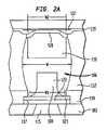
本発明の実施形態によれば、パッケージ化された超小型電子素子は、前面と、前面から離れる方に延伸している複数の第1の固体金属バンプと、を有している超小型電子素子を含む。ポストの各々は、前面の方向における幅および前面から延びる高さを有しており、高さは、幅の少なくとも半分になっている。また、上面と、上面から延伸して可融性金属によって第1の固体金属ポストに接合されている複数の第2の固体金属ポストと、を有している基板が設けられている。第2のポストは、上面および基板の前記上面から離れる方に急角度で延伸している縁面を備えている。 According to an embodiment of the present invention, a packaged microelectronic element has a front surface and a plurality of first solid metal bumps extending away from the front surface. including. Each of the posts has a width in the direction of the front surface and a height extending from the front surface, the height being at least half of the width. Also provided is a substrate having an upper surface and a plurality of second solid metal posts extending from the upper surface and joined to the first solid metal post by a fusible metal. The second post includes an upper surface and an edge surface extending at a steep angle away from the upper surface of the substrate.
この実施形態のポストは、エッチングによって形成されていてもよく、また本質的に銅を含むことができる。加えて、アンダーバンプ金属化物が、第1のバンプの下に配置されていてもよい。第1のポストの直径の、第1のポスト間のピッチへの比率は、3:4を超えないようにすることができる。さらに、第1のポストの直径は、第1のポストの各々間のピッチの半分より小さくすることができる。 The posts in this embodiment may be formed by etching and may essentially contain copper. In addition, an underbump metallization may be disposed under the first bump. The ratio of the diameter of the first post to the pitch between the first posts may not exceed 3: 4. Further, the diameter of the first post can be less than half the pitch between each of the first posts.
他の実施形態では、パッケージ化された超小型電子素子は、前面と、前面から離れる方に延伸している複数の第1の固体金属ポストと、を有している超小型電子素子を備えている。各ポストは、前面の方向における幅および前面から延びる高さを有しており、高さは幅の少なくとも半分となっている。また、上面と、上面から延伸して第1の固体金属ポストに接合されている複数の第2の固体金属ポストと、を有している基板が、設けられている。この実施形態では、第1のポストおよび第2のポストは、互いに拡散接合されている。 In another embodiment, a packaged microelectronic element comprises a microelectronic element having a front surface and a plurality of first solid metal posts extending away from the front surface. Yes. Each post has a width in the direction of the front surface and a height extending from the front surface, the height being at least half the width. A substrate having an upper surface and a plurality of second solid metal posts extending from the upper surface and bonded to the first solid metal post is provided. In this embodiment, the first post and the second post are diffusion bonded to each other.
第1のポストの直径の、第1のポスト間のピッチへの比率は、3:4を超えないようにすることができる。超小型電子素子の前面と基板の上面との間の距離は、80μmよりも大きくなっていてもよい。さらに、第1のポストの各々は、第2の金属ポストの各々の直径と等しい直径を有することもできる。最後に、アンダーフィル材が、超小型電子素子の前面と基板の上面との間に堆積されていてもよい。 The ratio of the diameter of the first post to the pitch between the first posts may not exceed 3: 4. The distance between the front surface of the microelectronic element and the upper surface of the substrate may be greater than 80 μm. Further, each of the first posts can have a diameter equal to the diameter of each of the second metal posts. Finally, an underfill material may be deposited between the front surface of the microelectronic element and the top surface of the substrate.
さらに他の実施形態では、パッケージ化された超小型電子素子は、前面と、前面から離れる方に延伸している複数の第1の固体金属ポストと、を有している超小型電子素子を備えている。各ポストは、前面の方向における幅および前面から延びる高さを有している。ポストは、本質的に半田または鉛または錫以外の金属を含む。また、上面を有している基板が設けられている。第1の固体金属ポストまたは第2の固体金属ポストの直径の、複数の第2の固体金属ポストが、上面から延伸して可融性金属によって第1の固体金属ポストに接合されている。複数の第1の固体金属ポストまたは複数の第2の固体金属ポスト間のピッチへの比率は、3:4を超えない。 In yet another embodiment, a packaged microelectronic element comprises a microelectronic element having a front surface and a plurality of first solid metal posts extending away from the front surface. ing. Each post has a width in the direction of the front surface and a height extending from the front surface. The post essentially comprises a metal other than solder or lead or tin. A substrate having an upper surface is also provided. A plurality of second solid metal posts having a diameter of the first solid metal post or the second solid metal post are extended from the upper surface and joined to the first solid metal post by a fusible metal. The ratio to pitch between the plurality of first solid metal posts or the plurality of second solid metal posts does not exceed 3: 4.
この実施形態の代替例では、基板は、多層基板とすることができる。加えて、第1のポストの直径は、第1のポストの各々間のピッチの半分よりも小さくすることができる。さらに、前記第1のポストの各々は、第2の金属ポストの直径と等しい直径を有していてもよい。 In an alternative to this embodiment, the substrate can be a multilayer substrate. In addition, the diameter of the first posts can be less than half the pitch between each of the first posts. Further, each of the first posts may have a diameter equal to the diameter of the second metal post.
他の実施形態では、パッケージ化された超小型電子素子は、前面と、前面から離れる方に延伸している複数の第1の固体金属ポストと、を有している超小型電子素子を含む。各ポストは、前面の方向における幅および前面から延びる高さを有している。また、上面を有している基板が設けられている。複数の第2の固体金属ポストが、上面から延伸して第1の固体金属ポストに接合されている。第1のポストのピッチは、50μmから200μmの範囲内にあり、超小型電子素子の底面と基板の上面との間の距離は、80μmよりも大きい。 In other embodiments, the packaged microelectronic element includes a microelectronic element having a front surface and a plurality of first solid metal posts extending away from the front surface. Each post has a width in the direction of the front surface and a height extending from the front surface. A substrate having an upper surface is also provided. A plurality of second solid metal posts are extended from the upper surface and joined to the first solid metal posts. The pitch of the first posts is in the range of 50 μm to 200 μm, and the distance between the bottom surface of the microelectronic element and the top surface of the substrate is greater than 80 μm.
この実施形態の代替例では、第2のポストを第1のポストに接合するのに、可融性金属が用いられることができる。第1のポストの各々は、第2の金属ポストの直径と等しい直径を有することができる。さらに、第1のポストの直径は、第1のポストの各々間のピッチの半分よりも小さくすることができる。 In an alternative to this embodiment, a fusible metal can be used to join the second post to the first post. Each of the first posts can have a diameter equal to the diameter of the second metal post. Furthermore, the diameter of the first post can be smaller than half the pitch between each of the first posts.
他の実施形態では、パッケージ化された超小型電子素子は、超小型電子素子と、基板と、超小型電子素子と基板との間に延伸する複数のピラーと、を含む。複数のピラーの各々は、超小型電子素子に取り付けられた第1の金属ポスト部分と、基板に取り付けられた第2の金属ポスト部分と、金属融着部分と、を備えており、第1の金属部分および第2の金属部分は、互いに接合されている。複数のピラーは、50μmより小さくない長さを有する。第1の金属ポスト部分および第2の金属ポスト部分の高さは、幅の少なくとも半分となっている。 In another embodiment, a packaged microelectronic element includes a microelectronic element, a substrate, and a plurality of pillars extending between the microelectronic element and the substrate. Each of the plurality of pillars includes a first metal post portion attached to the microelectronic element, a second metal post portion attached to the substrate, and a metal fusion portion. The metal part and the second metal part are joined to each other. The plurality of pillars have a length not smaller than 50 μm. The height of the first metal post portion and the second metal post portion is at least half of the width.
この実施形態の代替案では、超小型電子素子の前面と基板の上面との間の距離は、80μmよりも大きい。また、基板は、多層基板とすることができる。 In an alternative to this embodiment, the distance between the front surface of the microelectronic element and the top surface of the substrate is greater than 80 μm. The substrate can be a multilayer substrate.
第1のポストの各々は、第2の金属ポストの直径と等しい直径を有することができる。第1のポストの直径は、第1のポストの各々間のピッチの半分よりも小さくすることができる。加えて、第1のポストまたは第2のポストは、エッチングによって形成することができる。 Each of the first posts can have a diameter equal to the diameter of the second metal post. The diameter of the first post can be less than half the pitch between each of the first posts. In addition, the first post or the second post can be formed by etching.
パッケージ化された超小型電子素子アセンブリを製造する方法は、超小型電子素子の第1の面から離れる方に延伸している複数の導電性ポストを有する超小型電子素子を設けるステップを含んでいる。ポストは、上面および上面から離れる方に急角度で延伸している縁面を有している。可融性金属キャップが、複数の導電性ポストの各々の端に取り付けられている。次のステップは、超小型電子素子のポストを基板の第1の面から延伸している複数のポストに少なくとも実質的に一直線に並べることを含んでいる。最後のステップは、超小型電子素子のポストを基板のポストに接合することを含んでいる。 A method of manufacturing a packaged microelectronic element assembly includes providing a microelectronic element having a plurality of conductive posts extending away from a first surface of the microelectronic element. . The post has an upper surface and an edge surface extending at a steep angle away from the upper surface. A fusible metal cap is attached to each end of the plurality of conductive posts. The next step includes aligning the microelectronic element posts at least substantially in a plurality of posts extending from the first surface of the substrate. The final step involves bonding the microelectronic element post to the substrate post.
代替的方法では、ステップ(c)は、可融性金属を融点まで加熱し、可融性金属をポストの縁面の露出した部分上に流動させることを含んでいる。 In an alternative method, step (c) includes heating the fusible metal to the melting point and causing the fusible metal to flow over the exposed portion of the post edge.
他の代替的方法では、不動態化層およびアンダーバンプ金属化層が、超小型電子素子の上に堆積されている。 In another alternative method, a passivation layer and an underbump metallization layer are deposited on the microelectronic element.
以下のパラグラフは、ここでの種々の実施形態を述べるものである。 The following paragraphs describe various embodiments herein.
1.パッケージ化された超小型電子素子において、
前面と、前面から離れる方に延伸している複数の第1の固体金属バンプと、を有している超小型電子素子であって、各ポストは、前面の方向における幅および前面から延びる高さを有しており、高さは、前記幅の少なくとも半分になっている、超小型電子素子と、
上面と、上面から延伸して可融性金属によって第1の固体金属ポストに接合されている複数の第2の固体金属ポストと、を有する基板であって、前記ポストは、上面および前記上面から離れる方に急角度で延伸している縁面を有する、基板と、
を備えるパッケージ化された超小型電子素子。1. In packaged microelectronic elements,
A microelectronic element having a front surface and a plurality of first solid metal bumps extending away from the front surface, each post having a width in the direction of the front surface and a height extending from the front surface A microelectronic element having a height at least half of the width; and
A substrate having a top surface and a plurality of second solid metal posts extending from the top surface and joined to the first solid metal post by a fusible metal, the posts from the top surface and the top surface A substrate having an edge extending at a steep angle away from the substrate;
A packaged microelectronic element comprising:
2.前記第1のバンプまたは前記第2のポストは、銅を含むパラグラフ1に記載のパッケージ化された超小型電子素子。 2. The packaged microelectronic element according to paragraph 1, wherein the first bump or the second post includes copper.
3.前記可融性金属は、本質的に、半田または錫または共晶材料から成る群から選択されるパラグラフ1に記載のパッケージ化された超小型電子素子。 3. The packaged microelectronic element of paragraph 1, wherein the fusible metal is selected from the group consisting essentially of solder or tin or a eutectic material.
4.前記第1のバンプ間のピッチは、50μmから200μmの範囲内にあるようになっていることを特徴とするパラグラフ1に記載のパッケージ化された超小型電子素子。 4). The packaged microelectronic element according to paragraph 1, wherein the pitch between the first bumps is in the range of 50 μm to 200 μm.
5.前記第1のバンプの直径の、前記第1のポスト間のピッチへの比率は、3:4を超えないパラグラフ1に記載のパッケージ化された超小型電子素子。 5. The packaged microelectronic element of paragraph 1, wherein the ratio of the diameter of the first bump to the pitch between the first posts does not exceed 3: 4.
6.前記超小型電子素子の前記前面と前記基板の前記上面との間の距離は、80μmよりも大きいパラグラフ1に記載のパッケージ化された超小型電子素子。 6). The packaged microelectronic element according to paragraph 1, wherein the distance between the front surface of the microelectronic element and the top surface of the substrate is greater than 80 μm.
7.前記第1のバンプの下に位置するアンダーバンプ金属化物をさらに備えるパラグラフ1に記載のパッケージ化された超小型電子素子。 7). The packaged microelectronic element of paragraph 1, further comprising an underbump metallization located under the first bump.
8.前記基板は、多層基板であるパラグラフ1に記載のパッケージ化された超小型電子素子。 8). The packaged microelectronic element according to paragraph 1, wherein the substrate is a multilayer substrate.
9.前記第1のバンプの各々は、前記第2のポストの直径と等しい直径を有するパラグラフ1に記載のパッケージ化された超小型電子素子。 9. The packaged microelectronic element of paragraph 1, wherein each of the first bumps has a diameter equal to the diameter of the second post.
10.前記第1のバンプの直径は、前記第1のポストの各々間のピッチの半分よりも小さいパラグラフ1に記載のパッケージ化された超小型電子素子。 10. The packaged microelectronic element according to paragraph 1, wherein the diameter of the first bump is less than half the pitch between each of the first posts.
11.前記超小型電子素子の前記前面と前記基板の前記上面との間にアンダーフィル材をさらに備えるパラグラフ1に記載のパッケージ化された超小型電子素子。 11. The packaged microelectronic element of paragraph 1, further comprising an underfill material between the front surface of the microelectronic element and the upper surface of the substrate.
12.前記超小型電子素子の前記前面を覆っている半田マスクの層をさらに備えるパラグラフ1に記載のパッケージ化された超小型電子素子。 12 The packaged microelectronic element of paragraph 1, further comprising a solder mask layer covering the front surface of the microelectronic element.
13.前記第1のポストまたは前記第2のポストは、エッチングによって形成されるパラグラフ1に記載のパッケージ化された超小型電子素子。 13. The packaged microelectronic element according to paragraph 1, wherein the first post or the second post is formed by etching.
14.前記第1のポストまたは前記第2のポストは、電気メッキによって形成されるパラグラフ1に記載のパッケージ化された超小型電子素子。 14 The packaged microelectronic element according to paragraph 1, wherein the first post or the second post is formed by electroplating.
15.前記前面は、動作面であるパラグラフ1に記載のパッケージ化された超小型電子素子。 15. The packaged microelectronic element according to paragraph 1, wherein the front surface is an operating surface.
16.トレースが、前記超小型電子素子の前記前面に沿って伸びているパラグラフ1に記載のパッケージ化された超小型電子素子。 16. The packaged microelectronic element of paragraph 1, wherein traces extend along the front surface of the microelectronic element.
17.前記基板は、第2の面をさらに備えており、前記第2のポストと前記基板の前記底面に露出した回路との間に接続をもたらすために、ビアが前記基板を貫通しているパラグラフ1に記載のパッケージ化された超小型電子素子。 17. Paragraph 1 wherein the substrate further comprises a second surface and vias pass through the substrate to provide a connection between the second post and circuitry exposed on the bottom surface of the substrate. A packaged microelectronic device as described in 1.
18.パッケージ化された超小型電子素子において、
前面と、前面から離れる方に延伸する複数の第1の固体金属ポストと、を有する超小型電子素子であって、各ポストは、前面の方向における幅および前面から延びる高さを有しており、高さは、前記幅の少なくとも半分である、超小型電子素子と、
上面と、上面から延伸して第1の固体金属ポストに接合されている複数の第2の固体金属ポストと、を有する基板であって、前記第1のポストおよび前記第2のポストは、互いに拡散接合されている、基板と、
を備えるパッケージ化された超小型電子素子。18. In packaged microelectronic elements,
A microelectronic element having a front surface and a plurality of first solid metal posts extending away from the front surface, each post having a width in the direction of the front surface and a height extending from the front surface A microelectronic element whose height is at least half of said width;
A substrate having a top surface and a plurality of second solid metal posts extending from the top surface and joined to the first solid metal post, wherein the first post and the second post are A diffusion bonded substrate;
A packaged microelectronic element comprising:
19.前記第1のポストまたは前記第2のポストは、銅を含んむパラグラフ18に記載のパッケージ化された超小型電子素子。 19. The packaged microelectronic element of paragraph 18 wherein the first post or the second post comprises copper.
20.前記第1のポスト間のピッチは、50μmから200μmの範囲内であるパラグラフ18に記載のパッケージ化された超小型電子素子。 20. The packaged microelectronic element of paragraph 18 wherein the pitch between the first posts is in the range of 50 μm to 200 μm.
21.前記第1のポストの直径の、前記第1のポスト間のピッチへの比率は、3:4を超えないパラグラフ18に記載のパッケージ化された超小型電子素子。 21. The packaged microelectronic element according to paragraph 18, wherein the ratio of the diameter of the first posts to the pitch between the first posts does not exceed 3: 4.
22.前記超小型電子素子の前記前面と前記基板の前記上面との間の距離は、80μmよりも大きいパラグラフ18に記載のパッケージ化された超小型電子素子。 22. The packaged microelectronic element of paragraph 18, wherein the distance between the front surface of the microelectronic element and the top surface of the substrate is greater than 80 μm.
23.前記第1のポストの下に位置するアンダーバンプ金属化物をさらに備えるパラグラフ18に記載のパッケージ化された超小型電子素子。 23. The packaged microelectronic element of paragraph 18 further comprising an underbump metallization located under the first post.
24.前記基板は、多層基板であるパラグラフ18に記載のパッケージ化された超小型電子素子。 24. The packaged microelectronic element of paragraph 18 wherein the substrate is a multilayer substrate.
25.前記第1のポストの各々は、前記第2の金属ポストの各々の直径と等しい直径を有するパラグラフ18に記載のパッケージ化された超小型電子素子。 25. The packaged microelectronic element of paragraph 18 wherein each of the first posts has a diameter equal to the diameter of each of the second metal posts.
26.前記第1のポストの直径は、前記第1のポストの各々間のピッチの半分よりも小さいパラグラフ18に記載のパッケージ化された超小型電子素子。 26. The packaged microelectronic element of paragraph 18 wherein the diameter of the first post is less than half the pitch between each of the first posts.
27.前記超小型電子素子の前記前面と前記基板の前記上面との間にアンダーフィル材をさらに備えるパラグラフ18に記載のパッケージ化された超小型電子素子。 27. The packaged microelectronic element according to paragraph 18, further comprising an underfill material between the front surface of the microelectronic element and the upper surface of the substrate.
28.前記超小型電子素子の前記前面を覆っている半田マスクの層をさらに備えるパラグラフ18に記載のパッケージ化された超小型電子素子。 28. 19. The packaged microelectronic element of paragraph 18, further comprising a solder mask layer covering the front surface of the microelectronic element.
29.前記第1のポストまたは前記第2のポストは、エッチングによって形成されるパラグラフ18に記載のパッケージ化された超小型電子素子。 29. 19. The packaged microelectronic element according to paragraph 18, wherein the first post or the second post is formed by etching.
30.前記第1のポストまたは前記第2のポストは、電気メッキによって形成されるパラグラフ18に記載のパッケージ化された超小型電子素子。 30. The packaged microelectronic element according to paragraph 18, wherein the first post or the second post is formed by electroplating.
31.前記前面は、動作面であるパラグラフ18に記載のパッケージ化された超小型電子素子。 31. The packaged microelectronic element according to paragraph 18, wherein the front surface is an operating surface.
32.トレースが、前記超小型電子素子の前記前面に沿って伸びているパラグラフ18に記載のパッケージ化された超小型電子素子。 32. The packaged microelectronic element of paragraph 18 wherein traces extend along the front surface of the microelectronic element.
33.前記基板は、第2の面をさらに備えており、前記第2のポストと前記基板の前記底面に露出した回路との間に接続をもたらすために、ビアが前記基板を貫通しているパラグラフ18に記載のパッケージ化された超小型電子素子。 33. Paragraph 18 further includes a second surface, wherein vias pass through the substrate to provide a connection between the second post and circuitry exposed on the bottom surface of the substrate. A packaged microelectronic device as described in 1.
34.パッケージ化された超小型電子素子において、
前面と、前面から離れる方に延伸している複数の第1の固体金属ポストと、を有している超小型電子素子であって、各ポストは、前面の方向における幅および前面から延びる高さを有しており、前記ポストは、本質的に、半田または鉛または錫以外の金属から成っている、超小型電子素子と、
上面と、上面から延伸して可融性金属によって第1の固体金属ポストに接合されている複数の第2の固体金属ポストと、を有している基板と、
を備えており、
前記第1の固体金属ポストまたは前記第2の固体金属ポストの直径の、前記複数の第1の固体金属ポストまたは前記複数の第2の固体金属ポスト間のピッチへの比率は、3:4を超えないパッケージ化された超小型電子素子。34. In packaged microelectronic elements,
A microelectronic element having a front surface and a plurality of first solid metal posts extending away from the front surface, each post having a width in the direction of the front surface and a height extending from the front surface The post is essentially made of solder or a metal other than lead or tin, and a microelectronic element;
A substrate having an upper surface and a plurality of second solid metal posts extending from the upper surface and joined to the first solid metal post by a fusible metal;
With
The ratio of the diameter of the first solid metal post or the second solid metal post to the pitch between the plurality of first solid metal posts or the plurality of second solid metal posts is 3: 4. Packaged microelectronic elements that do not exceed.
35.前記第1のポストまたは前記第2のポストは、銅を含むパラグラフ34に記載のパッケージ化された超小型電子素子。 35. 35. A packaged microelectronic element according to paragraph 34, wherein the first post or the second post comprises copper.
36.前記可融性金属は、本質的に、半田または錫または共晶材料から成る群から選択される特徴とするパラグラフ34に記載のパッケージ化された超小型電子素子。 36. 35. The packaged microelectronic element of paragraph 34, wherein the fusible metal is selected from the group consisting essentially of solder or tin or a eutectic material.
37.前記第1のポスト間のピッチは、50μmから200μmの範囲内であるパラグラフ34に記載のパッケージ化された超小型電子素子。 37. 35. The packaged microelectronic element according to paragraph 34, wherein the pitch between the first posts is in the range of 50 μm to 200 μm.
38.前記超小型電子素子の前記前面と前記基板の前記上面との間の距離は、80μmよりも大きいパラグラフ34に記載のパッケージ化された超小型電子素子。 38. 35. The packaged microelectronic element of paragraph 34, wherein the distance between the front surface of the microelectronic element and the top surface of the substrate is greater than 80 μm.
39.前記第1のポストの下に位置するアンダーバンプ金属化物をさらに備えるパラグラフ34に記載のパッケージ化された超小型電子素子。 39. 35. The packaged microelectronic element of paragraph 34, further comprising an underbump metallization located under the first post.
40.前記基板は、多層基板であるパラグラフ34に記載のパッケージ化された超小型電子素子。 40. 35. A packaged microelectronic element according to paragraph 34, wherein the substrate is a multilayer substrate.
41.前記第1のポストの各々は、前記第2の金属ポストの各々の直径と等しい直径を有するパラグラフ34に記載のパッケージ化された超小型電子素子。 41. 35. The packaged microelectronic element of paragraph 34, wherein each of the first posts has a diameter equal to the diameter of each of the second metal posts.
42.前記第1のポストの直径は、前記第1のポストの各々間のピッチの半分よりも小さいパラグラフ34に記載のパッケージ化された超小型電子素子。 42. 35. The packaged microelectronic element of paragraph 34, wherein the diameter of the first post is less than half the pitch between each of the first posts.
43.前記超小型電子素子の前記前面と前記基板の前記上面との間にアンダーフィル材をさらに備えるパラグラフ34に記載のパッケージ化された超小型電子素子。 43. 35. The packaged microelectronic element of paragraph 34, further comprising an underfill material between the front surface of the microelectronic element and the upper surface of the substrate.
44.前記超小型電子素子の前記前面を覆っている半田マスクの層をさらに備えるパラグラフ34に記載のパッケージ化された超小型電子素子。 44. 35. The packaged microelectronic element of paragraph 34, further comprising a solder mask layer covering the front surface of the microelectronic element.
45.前記第1のポストまたは前記第2のポストは、エッチングによって形成されるパラグラフ34に記載のパッケージ化された超小型電子素子。 45. 35. The packaged microelectronic element according to paragraph 34, wherein the first post or the second post is formed by etching.
46.前記第1のポストまたは前記第2のポストは、電気メッキによって形成されるパラグラフ34に記載のパッケージ化された超小型電子素子。 46. 35. The packaged microelectronic element according to paragraph 34, wherein the first post or the second post is formed by electroplating.
47.前記前面は、動作面であるパラグラフ34に記載のパッケージ化された超小型電子素子。 47. 35. The packaged microelectronic element of paragraph 34, wherein the front surface is an operating surface.
48.トレースが、前記超小型電子素子の前記前面に沿って伸びているパラグラフ34に記載のパッケージ化された超小型電子素子。 48. 35. The packaged microelectronic element of paragraph 34, wherein a trace extends along the front surface of the microelectronic element.
49.前記基板は、第2の面をさらに備えており、前記第2のポストと前記基板の前記底面に露出した回路との間に接続をもたらすために、ビアが前記基板を貫通しているパラグラフ34に記載のパッケージ化された超小型電子素子。 49. Paragraph 34 wherein the substrate further comprises a second surface, and vias pass through the substrate to provide a connection between the second post and circuitry exposed on the bottom surface of the substrate. A packaged microelectronic device as described in 1.
50.パッケージ化された超小型電子素子において、
前面と、前面から離れる方に延伸している複数の第1の固体金属ポストと、を有している超小型電子素子であって、各ポストは、前面の方向における幅および前面から延びる高さを有している、超小型電子素子と、
上面と、上面から延伸して第1の固体金属ポストに接合されている複数の第2の固体金属ポストと、を有している基板であって、前記第1のポストのピッチは、50μmから200μmの範囲内にあり、前記超小型電子素子の前記底面と前記基板の前記上面との間の距離は、80μmよりも大きい、基板と、
を備えていることを特徴とするパッケージ化された超小型電子素子。50. In packaged microelectronic elements,
A microelectronic element having a front surface and a plurality of first solid metal posts extending away from the front surface, each post having a width in the direction of the front surface and a height extending from the front surface A microelectronic element having:
A substrate having a top surface and a plurality of second solid metal posts extending from the top surface and bonded to the first solid metal post, wherein the pitch of the first posts is from 50 μm A distance between the bottom surface of the microelectronic element and the top surface of the substrate that is greater than 80 μm,
A packaged microelectronic element characterized by comprising:
51.前記第1のポストまたは前記第2のポストは、銅を含んでいるパラグラフ50に記載のパッケージ化された超小型電子素子。 51. 51. A packaged microelectronic element according to paragraph 50, wherein the first post or the second post includes copper.
52.前記第2のポストを前記第1のポストに接合させるのに、可融性金属が用いられているパラグラフ50に記載のパッケージ化された超小型電子素子。 52. 51. The packaged microelectronic element of paragraph 50, wherein a fusible metal is used to join the second post to the first post.
53.前記可融性金属は、本質的に、半田または錫または共晶材料から成る群から選択されるパラグラフ50に記載のパッケージ化された超小型電子素子。 53. 51. A packaged microelectronic element according to paragraph 50, wherein the fusible metal is selected from the group consisting essentially of solder or tin or a eutectic material.
54.前記第1のポストの直径の、前記第1のポスト間のピッチへの比率は、3:4を超えないパラグラフ50に記載のパッケージ化された超小型電子素子。 54. 51. The packaged microelectronic element of paragraph 50, wherein the ratio of the diameter of the first post to the pitch between the first posts does not exceed 3: 4.
55.前記超小型電子素子の前記前面と前記基板の前記上面との間の距離は、80μmよりも大きいパラグラフ50に記載のパッケージ化された超小型電子素子。 55. 51. A packaged microelectronic element according to paragraph 50, wherein a distance between the front surface of the microelectronic element and the top surface of the substrate is greater than 80 μm.
56.前記第1のポストの下に位置するアンダーバンプ金属化物をさらに備えるパラグラフ50に記載のパッケージ化された超小型電子素子。 56. 52. The packaged microelectronic element of paragraph 50, further comprising an underbump metallization located under the first post.
57.前記基板は、多層基板であるパラグラフ50に記載のパッケージ化された超小型電子素子。 57. 51. The packaged microelectronic element according to paragraph 50, wherein the substrate is a multilayer substrate.
58.前記第1のポストの各々は、前記第2の金属ポストの直径と等しい直径を有しているパラグラフ50に記載のパッケージ化された超小型電子素子。 58. 51. A packaged microelectronic element according to paragraph 50, wherein each of said first posts has a diameter equal to the diameter of said second metal post.
59.前記第1のポストの直径は、前記第1のポストの各々間のピッチの半分よりも小さいパラグラフ50に記載のパッケージ化された超小型電子素子。 59. 51. The packaged microelectronic element of paragraph 50, wherein the diameter of the first post is less than half of the pitch between each of the first posts.
60.前記超小型電子素子の前記前面と前記基板の前記上面との間にアンダーフィル材をさらに備えているパラグラフ50に記載のパッケージ化された超小型電子素子。 60. 51. The packaged microelectronic element of paragraph 50, further comprising an underfill material between the front surface of the microelectronic element and the top surface of the substrate.
61.前記超小型電子素子の前記前面を覆っている半田マスクの層をさらに備えているパラグラフ50に記載のパッケージ化された超小型電子素子。 61. 51. The packaged microelectronic element of paragraph 50, further comprising a solder mask layer covering the front surface of the microelectronic element.
62.前記第1のポストまたは前記第2のポストは、エッチングによって形成されているパラグラフ50に記載のパッケージ化された超小型電子素子。 62. 51. A packaged microelectronic element according to paragraph 50, wherein the first post or the second post is formed by etching.
63.前記第1のポストまたは前記第2のポストは、電気メッキによって形成されているパラグラフ50に記載のパッケージ化された超小型電子素子。 63. 51. The packaged microelectronic element according to paragraph 50, wherein the first post or the second post is formed by electroplating.
64.前記前面は、動作面であるパラグラフ50に記載のパッケージ化された超小型電子素子。 64. 51. The packaged microelectronic element of paragraph 50, wherein the front surface is an operational surface.
65.トレースが、前記超小型電子素子の前記前面に沿って伸びているパラグラフ50に記載のパッケージ化された超小型電子素子。 65. The packaged microelectronic element of paragraph 50, wherein a trace extends along the front surface of the microelectronic element.
66.前記基板は、第2の面をさらに備えており、前記第2のポストと前記基板の前記底面に露出した回路との間に接続をもたらすために、ビアが前記基板を貫通していることを特徴とするパラグラフ50に記載のパッケージ化された超小型電子素子。 66. The substrate further comprises a second surface, and vias pass through the substrate to provide a connection between the second post and a circuit exposed on the bottom surface of the substrate. 56. The packaged microelectronic element of paragraph 50, characterized.
67.パッケージ化された超小型電子素子において、
前面と、前面から離れる方に延伸している複数の第1の固体金属ポストと、を有している超小型電子素子であって、各ポストは、前面の方向における幅および前面から延びる高さを有している、超小型電子素子と、
上面と、上面から延伸して第1の固体金属ポストに接合されている複数の第2の固体金属ポストと、を有している基板と、
を備えており、
前記複数の第1の固体金属ポストおよび前記複数の第2の固体金属ポストが、本質的に銅から成っているパッケージ化された超小型電子素子。67. In packaged microelectronic elements,
A microelectronic element having a front surface and a plurality of first solid metal posts extending away from the front surface, each post having a width in the direction of the front surface and a height extending from the front surface A microelectronic element having:
A substrate having an upper surface and a plurality of second solid metal posts extending from the upper surface and bonded to the first solid metal post;
With
A packaged microelectronic element, wherein the plurality of first solid metal posts and the plurality of second solid metal posts are essentially made of copper.
68.第1のポストおよび第2のポストを接合させるのに、可融性金属が用いられているパラグラフ67に記載のパッケージ化された超小型電子素子。 68. 68. The packaged microelectronic element of paragraph 67, wherein a fusible metal is used to join the first post and the second post.
69.前記可融性金属は、本質的に、半田または錫または共晶材料から成る群から選択されるパラグラフ68に記載のパッケージ化された超小型電子素子。 69. 69. A packaged microelectronic element according to paragraph 68, wherein the fusible metal is selected from the group consisting essentially of solder or tin or a eutectic material.
70.前記第1のポスト間のピッチは、50μmから200μmの範囲内であるパラグラフ67に記載のパッケージ化された超小型電子素子。 70. 68. The packaged microelectronic element of paragraph 67, wherein the pitch between the first posts is in the range of 50 μm to 200 μm.
71.前記第1のポストの直径の、前記第1のポスト間のピッチへの比率は、3:4を超えないパラグラフ67に記載のパッケージ化された超小型電子素子。 71. 68. The packaged microelectronic element of paragraph 67, wherein the ratio of the diameter of the first posts to the pitch between the first posts does not exceed 3: 4.
72.前記超小型電子素子の前記前面と前記基板の前記上面との間の距離は、80μmよりも大きいパラグラフ67に記載のパッケージ化された超小型電子素子。 72. 68. The packaged microelectronic element according to paragraph 67, wherein a distance between the front surface of the microelectronic element and the top surface of the substrate is greater than 80 μm.
73.前記第1のポストを覆っているアンダーバンプ金属化物をさらに備えているパラグラフ67に記載のパッケージ化された超小型電子素子。 73. 68. The packaged microelectronic element of paragraph 67, further comprising an underbump metallization covering the first post.
74.前記基板は、多層基板であるパラグラフ67に記載のパッケージ化された超小型電子素子。 74. 68. The packaged microelectronic element of paragraph 67, wherein the substrate is a multilayer substrate.
75.前記第1のポストの各々は、前記第2の金属ポストの直径と等しい直径を有しているパラグラフ67に記載のパッケージ化された超小型電子素子。 75. 68. The packaged microelectronic element of paragraph 67, wherein each of the first posts has a diameter equal to the diameter of the second metal post.
76.前記第1のポストの直径は、前記第1のポストの各々間のピッチの半分よりも小さいパラグラフ67に記載のパッケージ化された超小型電子素子。 76. 68. The packaged microelectronic element of paragraph 67, wherein the diameter of the first post is less than half the pitch between each of the first posts.
77.前記超小型電子素子の前記前面と前記基板の前記上面との間にアンダーフィル材をさらに備えているパラグラフ67に記載のパッケージ化された超小型電子素子。 77. 68. The packaged microelectronic element of paragraph 67, further comprising an underfill material between the front surface of the microelectronic element and the top surface of the substrate.
78.前記超小型電子素子の前記前面を覆っている半田マスクの層をさらに備えているパラグラフ67に記載のパッケージ化された超小型電子素子。 78. 68. The packaged microelectronic element of paragraph 67, further comprising a solder mask layer covering the front surface of the microelectronic element.
79.前記第1のポストまたは前記第2のポストは、エッチングによって形成されているパラグラフ67に記載のパッケージ化された超小型電子素子。 79. 68. The packaged microelectronic element according to paragraph 67, wherein the first post or the second post is formed by etching.
80.前記第1のポストまたは前記第2のポストは、電気メッキによって形成されているパラグラフ67に記載のパッケージ化された超小型電子素子。 80. 68. The packaged microelectronic element according to paragraph 67, wherein the first post or the second post is formed by electroplating.
81.前記前面は、動作面であるパラグラフ67に記載のパッケージ化された超小型電子素子。 81. 68. The packaged microelectronic element of paragraph 67, wherein the front surface is an operating surface.
82.トレースが、前記超小型電子素子の前記前面に沿って伸びているパラグラフ67に記載のパッケージ化された超小型電子素子。 82. 68. The packaged microelectronic element of paragraph 67, wherein traces extend along the front surface of the microelectronic element.
83.前記基板は、第2の面をさらに備えており、前記第2のポストと前記基板の前記底面に露出した回路との間に接続をもたらすために、ビアが前記基板を貫通していることを特徴とするパラグラフ67に記載のパッケージ化された超小型電子素子。 83. The substrate further comprises a second surface, and vias pass through the substrate to provide a connection between the second post and a circuit exposed on the bottom surface of the substrate. 68. A packaged microelectronic element according to paragraph 67 characterized.
84.パッケージ化された超小型電子素子において、
超小型電子素子と、基板と、前記超小型電子素子と前記基板との間に延伸している複数のピラーであって、各々が、前記超小型電子素子に取り付けられた第1の金属ポスト部分と、前記基板に取り付けられた第2の金属ポスト部分と、金属融着部分と、を備えている、複数のピラーと、を備えており、前記第1の金属部分および前記第2の金属部分は、互いに接合されており、前記複数のピラーは、50μm以上の長さを有しており、前記第1の金属ポスト部分および前記第2の金属ポスト部分の前記高さは、前記幅の少なくとも半分であるパッケージ化された超小型電子素子。84. In packaged microelectronic elements,
A microelectronic element, a substrate, and a plurality of pillars extending between the microelectronic element and the substrate, each of which is a first metal post portion attached to the microelectronic element And a plurality of pillars, each having a second metal post portion attached to the substrate and a metal fusion portion, and the first metal portion and the second metal portion. Are joined to each other, and the plurality of pillars have a length of 50 μm or more, and the height of the first metal post portion and the second metal post portion is at least the width of the first metal post portion. Half packaged microelectronic element.
85.前記第1のポストまたは前記第2のポストは、銅を含んでいるパラグラフ84に記載のパッケージ化された超小型電子素子。 85. 85. A packaged microelectronic element according to paragraph 84, wherein the first post or the second post includes copper.
86.前記第1のポスト間のピッチは、50μmから200μmの範囲内であるパラグラフ84に記載のパッケージ化された超小型電子素子。 86. 85. The packaged microelectronic element of paragraph 84, wherein the pitch between the first posts is in the range of 50 μm to 200 μm.
87.前記第1のポストの直径の、前記第1のポスト間のピッチへの比率は、3:4を超えないパラグラフ84に記載のパッケージ化された超小型電子素子。 87. 85. The packaged microelectronic element of paragraph 84, wherein the ratio of the diameter of the first post to the pitch between the first posts does not exceed 3: 4.
88.前記超小型電子素子の前記前面と前記基板の前記上面との間の距離は、80μmよりも大きいパラグラフ84に記載のパッケージ化された超小型電子素子。 88. 85. The packaged microelectronic element of paragraph 84, wherein the distance between the front surface of the microelectronic element and the top surface of the substrate is greater than 80 μm.
89.前記第1のポストの下に位置するアンダーバンプ金属化物をさらに備えているパラグラフ84に記載のパッケージ化された超小型電子素子。 89. 85. The packaged microelectronic element of paragraph 84, further comprising an underbump metallization located under the first post.
90.前記基板は、多層基板であるパラグラフ84に記載のパッケージ化された超小型電子素子。 90. 85. The packaged microelectronic element of paragraph 84, wherein the substrate is a multilayer substrate.
91.前記第1のポストの各々は、前記第2の金属ポストの直径と等しい直径を有しているパラグラフ84に記載のパッケージ化された超小型電子素子。 91. 85. A packaged microelectronic element according to paragraph 84, wherein each of said first posts has a diameter equal to the diameter of said second metal post.
92.前記第1のポストの直径は、前記第1のポストの各々間のピッチの半分よりも小さいパラグラフ84に記載のパッケージ化された超小型電子素子。 92. 85. A packaged microelectronic element according to paragraph 84, wherein the diameter of the first post is less than half the pitch between each of the first posts.
93.前記超小型電子素子の前記前面と前記基板の前記上面との間にアンダーフィル材をさらに備えるパラグラフ84に記載のパッケージ化された超小型電子素子。 93. 85. The packaged microelectronic element of paragraph 84, further comprising an underfill material between the front surface of the microelectronic element and the upper surface of the substrate.
94.前記超小型電子素子の前記前面を覆っている半田マスクの層をさらに備えるパラグラフ84に記載のパッケージ化された超小型電子素子。 94. 85. The packaged microelectronic element of paragraph 84, further comprising a solder mask layer covering the front surface of the microelectronic element.
95.前記第1のポストまたは前記第2のポストは、エッチングによって形成されているパラグラフ84に記載のパッケージ化された超小型電子素子。 95. 85. A packaged microelectronic element according to paragraph 84, wherein the first post or the second post is formed by etching.
96.前記第1のポストまたは前記第2のポストは、電気メッキによって形成されているパラグラフ84に記載のパッケージ化された超小型電子素子。 96. 85. A packaged microelectronic element according to paragraph 84, wherein the first post or the second post is formed by electroplating.
97.前記前面は、動作面であるパラグラフ84に記載のパッケージ化された超小型電子素子。 97. 85. The packaged microelectronic element of paragraph 84, wherein the front surface is an operating surface.
98.トレースが、前記超小型電子素子の前記前面に沿って延伸しているパラグラフ84に記載のパッケージ化された超小型電子素子。 98. 85. The packaged microelectronic element of paragraph 84, wherein a trace extends along the front surface of the microelectronic element.
99.前記基板は、第2の面をさらに備えており、前記第2のポストと前記基板の前記底面に露出した回路との間に接続をもたらすために、ビアが前記基板を貫通しているパラグラフ84に記載のパッケージ化された超小型電子素子。 99. Paragraph 84 wherein the substrate further comprises a second surface, and vias pass through the substrate to provide a connection between the second post and circuitry exposed on the bottom surface of the substrate. A packaged microelectronic device as described in 1.
ここで、図2に示されているパッケージ化された超小型電子アセンブリの構成部品の断面図を示している図1A〜1Cについて説明する。図示されているように、パッケージ化された超小型電子アセンブリ100は、基板102と、フェイスダウン位置、すなわち、フリップチップ位置にある超小型電子素子104と、基板を超小型電子素子に接合している導電性柱106と、を備えている。導電性柱は、基板102の面105から上方に突出している導電性バンプまたはポスト108を含んでおり、導電性ポスト108は、超小型電子素子104の面107から上方に突出している導電性バンプまたはポスト110と一直線に並んでいる。導電性柱106は、超小型電子素子104と基板102との間の隔離距離、すなわち、垂直方向距離を大きくすることによって、チップオン基板パッケージ化における高さを大きくし、同時に、導電性柱106間の水平方向の中心間距離またはピッチPを小さくすることを可能にするものである。以下にさらに詳細に説明するように、基板102と超小型電子素子104との間の距離を増大させる能力は、導電性柱の応力を低減するのに役立ち、アンダーフィル材112(図2A参照)の充填を容易にするのに役立ち、かつ極めて多様なアンダーフィル材を用いることを可能にする。 Reference is now made to FIGS. 1A-1C showing cross-sectional views of the components of the packaged microelectronic assembly shown in FIG. As shown, the packaged
図1Aを参照すると、基板102の例として、好ましくは、誘電体要素102Aが挙げられる。誘電体要素102Aは、上面101および反対側を向いている底面103を有している。複数の導電性トレース109が、この上面または底面に沿って延伸することもできるし、またはそれらの両面に沿って延伸することもできる。誘電体要素102Aは、剛性とすることもできるし、または柔軟性とすることもできる。誘電体要素102は、ポリイミドシートから成るようにすることもできるし、他のポリマーシートから成るようにすることもできる。誘電体要素102の厚みは、変更可能であるが、最も典型的には、2mm以下である。基板102は、他の導電性要素、例えば、底面103に露出した外部接点(図示せず)を備えていてもよい。接合トレースは、本発明の譲渡人に譲渡された米国特許公開出願第11/014,439号明細書に示されている方法を用いて、形成されていてもよい。この特許の開示内容は、参照することによって、ここに含まれるものとする。図示されている特定の実施形態では、導電性要素(図示せず)は、基板102の上面101上に配置されている。しかし、他の実施形態では、導電性要素は、基板102の底面103に沿って延伸していてもよいし、上面101および底面103の両面上または基板102の内部に延伸していてもよい。従って、この開示に用いられている「第1の特徴部が第2の特徴部の『上(on)』に配置されている」という記述は、第1の特徴部が第2の特徴部の表面上に位置していることを必要としていると理解されるべきではない。加えて、「上部(top)」、「底部(bottom)」、「上側(upper)」、および「下側(lower)」という記述的な用語は、説明することのみを目的として用いられている。 Referring to FIG. 1A, an example of the
また、基板102の上面101から、固体金属バンプまたは導電性ポスト108が延伸して、導電性柱106の第1の部分を形成している(図2および図2A)。導電性ポスト108は、上面111および縁面113を有している。縁面113は、基板102の上面から離れる方に急角度で延伸しており、これによって、区別可能な角度が、縁面113が基板102の上面101と交差する箇所に形成されている。例えば、図示されている実施形態では、90°よりも大きい角度が、基板102の上面101と導電性ポスト108の縁面113との間に形成されている。この角度は、導電性ポスト108の形状によって、異なることになる。例えば、円筒状ポストは、基板102の上面101と導電性ポスト108との間に90°の角度を有することができる。例示的なプロセスおよびポストは、2006年12月19日に出願された「チップキャパシタが埋め込まれたPWB」という表題の仮出願第60/875,730号、2007年8月15に出願された「相互接続ビア付き多層基板および該多層基板を製造する方法」という表題の仮出願第60/964,916号、および2007年8月15日に出願された「メッキによって形成されたポスト付き相互接続要素」という表題の仮出願第60/964,823号のそれぞれの明細書に記載されている。これらの全ての開示内容は、参照することによって、ここに含まれるものとする。例えば、導電性ポスト108は、ここでさらに詳細に述べるように、エッチングプロセスによって形成することもできる。代替的に、導電性ポスト108は、電気メッキによって形成することもでき、この場合、ポスト108は、フォトレジスト層のような誘電体層にパターン化された開口を通して金属基層上に金属をメッキすることによって、形成される。 A solid metal bump or
導電性ポスト108の寸法は、広範囲にわたって、変更可能である。しかし、最も典型的には、誘電体要素102Aの上面103から延びる各導電性ポスト108の高さH1は、少なくとも50μmであり、300μmまで延ばすことができる。これらの導電性ポスト108は、その直径または幅W1よりも大きい高さH1を有することができる。しかし、高さH1は、幅W1よりも小さくてもよく、例えば、幅W1の少なくとも半分とすることができる。 The dimensions of the
導電性ポスト108は、どのような導電性材料、例えば、銅、銅合金、金、およびそれらの組合せから作製することができる。導電性ポスト108は、半田濡れ性を有する少なくとも1つの露出金属を備えていてもよい。例えば、このポストは、該ポストの表面に金層を有する銅を含むことができる。加えて、導電性ポスト108は、該ポストが接合されることになる半田の融点よりも高い融点を有する少なくとも1つの金属層を含むことができる。例えば、このような導電性ポスト108は、銅の層を含んでいてもよいし、または全体が銅から形成されていてもよい。 The
また、導電性ポスト108は、切頭円錐形状を含む多くの異なる形状をとることもできる。導電性ポスト108の各々の基面114および先端116は、実質的に円形であってもよいし、または異なる形状、例えば、楕円形状を有していてもよい。導電性ポスト108の基面114は、典型的には、約50〜300μmの直径を有しており、先端116は、典型的には、約25〜200μmの直径を有している。各導電性ポスト108は、誘電体基板102に隣接する基面114および誘電性基板から離れた先端116を有することができる。加えて、(どのような半田マスクも除く)誘電体要素102Aの上面101からの導電性ポストの高さH1は、典型的には、わずかに30μmから200μmまでの範囲内にある。 The
図示されているように、半田マスク118(図2)が、基板102を覆ってかつ導電性ポスト108に隣接して、配置することができる。半田マスク118は、リフロー過程における半田のオーバーフローおよび互いに隣接する柱106間の橋掛けを防ぐのに役立つ。 As shown, a solder mask 118 (FIG. 2) can be placed over the
図1Bを参照すると、超小型電子素子104は、前面122および後面124を有している。超小型電子素子104は、好ましくは、パッケージング前および他の素子との相互接続前の半導体チップなどである。例えば、超小型電子素子は、ベアダイである。 Referring to FIG. 1B, the
超小型電子素子などから延伸することができる例示的な導電性ポストおよび導電性ポストを作製する方法が、Advanpak Solutions Pte. (「Advanpak」)社のウエブサイトおよびAdvanpak社に譲渡された米国特許第6,681,982号、第6,592,109号、および第6,578,754号のそれぞれの明細書に記載されている。これらの特許の開示内容は、参照することによって、ここに含まれるものとする。例えば、導電性ポスト110は、エッチングプロセスによって形成することができる。代替的に、導電性ポスト110は、電気メッキによって形成することができ、この場合、ポスト110は、フォトレジスト層にパターン化された開口を通して金属基層上に金属をメッキすることによって、形成される。基板から延伸している導電性ポスト108と同じように、超小型電子素子104から延伸しているポスト110は、上面111および縁面113を有することができる。縁面113は、超小型電子素子の前記上面122から離れる方に急角度で延伸しており、これによって、区別可能な角度が超小型電子素子と導電性ポストとの間に形成されるようになっている。 Exemplary conductive posts that can be stretched from microelectronic devices and the like, and methods for making conductive posts are disclosed in the Advanpak Solutions Pte. ("Advanpak") website and U.S. Patent No. assigned to Advanpak. 6,681,982, 6,592,109, and 6,578,754. The disclosures of these patents are hereby incorporated by reference. For example, the
導電性ポスト110と超小型電子素子104との間に金属接点をもたらすために、アンダーバンプ金属化層120が、超小型電子素子104の前面122上に設けることができる。アンダーバンプ金属化層120は、典型的には、チタン、チタン−タングステン、クロムを含む材料から成っている。アンダーバンプ金属化層120は、導電性柱106の導電性金属接点として作用するものである。保護層119が、当技術分野において周知の方法を用いて、超小型電子素子104の前面122上において、超小型電子素子104とアンダーバンプ金属化層120との間に設けることができる。 An under
図1B、図1C、図2を参照すると、超小型電子素子104から延伸している導電性ポスト110の寸法は、広範囲にわたって変更可能である。しかし、最も典型的には、各導電性ポスト110の高さH2は、50μmより小さくない。導電性ポスト110は、その幅W2よりも大きい高さH2を有することができる。しかし、この高さは、幅W2よりも小さくてもよく、例えば、幅の少なくとも半分とすることもできる。 Referring to FIGS. 1B, 1C, and 2, the dimensions of the
導電性ポスト110は、好ましくは、銅または銅合金から作製されているが、他の導電性材料、例えば、金または金と銅との組合せから作製されていてもよい。加えて、導電性ポスト110は、該ポストが接合される半田の融点よりも高い融点を有する少なくとも1つの金属層を備えていてもよい。例えば、このような導電性ポストは、銅の層を含んでいてもよいし、または全体が銅から形成されていてもよい。 The
特定の実施形態では、導電性ポスト110は、円筒形とすることができ、その結果、ポストの基面126の直径およびポストの先端128の直径は、実質的に互いに等しいことになる。一実施形態では、導電性ポストの基面126および先端128は、約30〜150μmの直径を有することができる。各導電性ポスト110は、基板102に隣接する基面126および基板102から離れた先端128を有することができる。代替的に、導電性ポスト110は、多種多様な形状、例えば、切頭円錐形状、矩形形状、またはバー形状を有することができる。 In certain embodiments, the
半田被膜または半田キャップ130が、導電性ポスト110の先端128、すなわち、超小型電子素子104に接続されていない部分に、取り付けることができる。半田キャップ130は、導電性ポスト110の直径または幅W2と同じ直径を有することができ、これによって、半田キャップ130は、導電性ポスト110の延長部をなすことになる。一例を挙げると、半田キャップ130は、略25〜80μmの範囲内にある高さH3を有することができる。 A solder coating or
超小型電子素子104の前面122から延伸している導電性ポスト110の高さH2は、誘電体要素102A(図1A)の上面101から延伸している導電性ポスト108の高さH1と等しくすることができることを理解されたい。しかし、これらの高さは、代替的に、異なっていてもよい。すなわち、導電性ポスト110の高さH2は、導電性ポスト108の高さH1よりも小さくてもよいし、または大きくてもよい。特定の実例では、超小型電子素子104から延伸している導電性ポスト110は、50μmの高さH2を有することができ、基板から延伸している導電性ポスト108は、55μmの高さH1を有することができる(図2)。 The height H2 of the
超小型電子素子104および基板102を互いに導電的に接続するために、超小型電子素子104の導電性ポスト110は、基板102上の導電性ポスト108に接続されなければならない。図1Cを参照すると、超小型電子素子104が反転され、超小型電子素子104の導電性ポスト110および基板102の導電性ポスト108は、互いに一直線に並んで近接して配置されている。超小型電子素子104上の半田キャップ130がリフローされ、半田が超小型電子素子104上の導電性ポスト110の表面および基板102上の導電性ポスト108の表面を濡らすことが可能になる。図2,2Aに示されているように、半田は、これらの導電性ポストの露出面を濡らし、超小型電子素子から基板に延伸する導電性柱106を形成する。超小型電子素子104および基板102の(半田が接合されている)導電性柱108,110の表面積が大きいことによって、半田界面における電流密度が小さくなる。このような電流密度の減少は、電子移動を低減させ、大きな耐久性を提供するのに役立つ。 In order to conductively connect the
図示されているように、導電性柱106は、導電性ポストを導電的に相互接続している半田を含む。超小型電子素子から延伸している導電性ポストの基面と基板から延伸している露出部の基面との間に延びている導電性柱の隔離距離または高さHは、一例では、80〜100μmの範囲内にある。 As shown, the
図2、図2Aを参照すると、導電性柱106の壁132は、凸形状または樽形状とすることができ、この場合、導電性柱の中点領域M(すなわち、超小型電子素子の導電性ポスト110と基板の導電性ポスト108との間の領域)は、基板102の上面101に隣接する導電性柱106の部分の幅W1および超小型電子素子104の前面102に隣接する導電性柱106の部分の幅W2のそれぞれよりも大きい幅Wを有している。 2 and 2A, the
図2Aにさらに示されているように、接触パッド117が、周知の方法を用いて、超小型電子素子104上および基板102上に形成することができる。一実施形態では、基板102から離れる方に延伸する下側ポスト108と、下側接触パッド117とは、例えば、2008年6月28日に公開された国際出願公開第2008/076428号パンフレットに開示されているような別々のエッチングプロセスによって、形成することができる。この開示内容は、参照することによってここに含まれるものとする。例えば、導電性ポスト108および接触パッド117を形成するために、上側金属層123、下側金属層123、および中間エッチングストップ層または内部金属層121を有する3金属(tri-metal)基板を用いることができる。1つのこのようなプロセスでは、3層以上の層状金属構造体の露出した金属層が、フォトリソグラフィーによってパターン化されたフォトレジスト層に従ってエッチングされ、導電性ポスト108を形成するようになっている。このとき、エッチングプロセスは、該構造体の内部金属層121において停止される。内部金属層121は、上下金属層123の金属と異なる一種または複数種の金属を含んでいる。具体的には、この内部金属層は、上側金属層123をエッチングするのに用いられるエッチング液によって侵食されない組成を有している。例えば、導電性ポスト108をエッチングによって形成することになる上側金属層123は、本質的に銅から成っており、下側金属層123も、本質的に銅から成っており、内部金属層121は、本質的にニッケルから成っている。ニッケルは、銅に対して良好な選択性を有しており、これによって、金属層がエッチングされて導電性ポスト108を形成するときに、ニッケル層の侵食が回避されることになる。接触パッド117を形成するには、フォトリソグラフィーによってパターン化された他のフォトレジスト層に従って、他のエッチングステップが行われるとよい。ポスト108は、ビア115のような他の導電性特徴部とさらに相互接続することができ、このビア115は、他の導電性特徴部(図示せず)にさらに相互接続することができる。 As further shown in FIG. 2A,
図3を参照すると、導電性柱106’の壁232は、真っ直ぐとすることができ、この場合、幅W5は、基板102’の上面101’に隣接する導電性柱106’の部分の幅W4および超小型電子素子104’の前面122’に隣接する導電性柱106’の部分の幅W4’のそれぞれにほぼ等しい。幅W4,W4’は、必ずしも互いに等しくなくてもよいことを理解されたい。代替的に、導電性柱106’の壁232’は、得られる所望の隔離距離に依存して、凹状とすることができる(図4参照)。 Referring to FIG. 3, the
本発明による導電性柱106は、誘電体要素と超小型電子素子との間の隔離高さを大きくすることを可能とすると共に、超小型電子素子104の前面122に露出した導電性ポスト110の各々間のピッチP(図1B,2参照)および基板102の上面101に露出した導電性ポスト108の各々間のピッチPを著しく小さくすることを可能とするものである。一実施形態では、ピッチPは、50μmほどの小さいものとすることができるし、または200μmほどの大きいものとすることができる。導電性柱108,110が互いに一直線に並んでいるという事実によって、導電性ポスト108の各々間のピッチPおよび導電性ポスト110の各々間のピッチPは、互いに等しくなることを理解されたい。 The
また、ピッチPは、導電性ポスト108,110の直径または幅W1,W2の関数とすることができる。具体的には、これらの導電性ポストのそれぞれの基面の直径W1,W2は、ピッチPの75%以下とすることができる。換言すると、ピッチPに対する直径W1,W2の比率は、3:4以下とすることができる。例えば、もしピッチPが145μmであるなら、導電性ポスト108,110の直径W1,W2は、108μm以下、すなわち、ピッチPの75%以下の範囲内とすることができる。 Also, the pitch P can be a function of the diameter or width W1, W2 of the
隔離高さを大きくすることによって、超小型電子素子内に含まれることがある低k誘電体材料の応力を低減させることができる。加えて、隔離距離の増大は、小さいピッチに概して関連付けられている問題、例えば、電子移動および電流集中(crowding)を最小限に抑えるのに役立つ。これは、導電性柱106が導電性ポスト108,110の表面を濡らすことができるという事実によるものである。 By increasing the isolation height, the stress of the low-k dielectric material that may be included in the microelectronic element can be reduced. In addition, the increase in isolation distance helps minimize problems generally associated with small pitches, such as electron transfer and current crowding. This is due to the fact that the
図5,6を参照すると、超小型電子素子上の導電性バンプを基板上の導電性バンプに接合する代替的構成が示されている。図5を参照すると、半田キャップ230は、超小型電子素子204から延伸している導電性ポスト210の先端228ではなく、基板202から延伸している導電性ポスト208の先端216に配置することができる。一実施形態では、半田キャップ230の幅または直径W5は、導電性ポスト208の基面214の直径W6と略等しくなっている。従って、半田キャップ230は、基板202から延伸している導電性ポスト208の先端216を超えて伸びている。しかし、いったん半田がリフローすると、導電性柱は、好ましくは、図2に示されている導電性柱の形状を取ることになる。 Referring to FIGS. 5 and 6, an alternative configuration for bonding conductive bumps on a microelectronic element to conductive bumps on a substrate is shown. Referring to FIG. 5, the
図6を参照すると、さらに他の代替的構成では、半田キャップ330は、第1の超小型電子素子304から延伸している導電性ポスト310の先端328、ならびに基板302から延伸している導電性ポスト308の先端316上に配置することができる。導電性ポスト308,310は、互いに近接して配置される。熱を加えると、半田キャップ330がリフローし、導電性ポスト308,310を濡らし、かつ互いに融着させる。いったんリフローすると、導電性柱306は、好ましくは、図2に示されている導電性柱306と同様の形状を取ることになる。Referring to FIG. 6, in yet another alternative configuration, the
図7を参照すると、超小型電子パッケージの代替的構成が示されている。この構成は、図2に示されているものと同様であり、唯一異なっているのは、基板から延伸している導電性ポストに隣接する半田マスクが存在していない点である。この代替的構成では、ビア407を用いて、導電性柱406を、基板402の上面401ではなく、基板402の底面403に露出している電子回路(図示せず)に導電的に接続することができるようになっている。ビア407を用いることによって、半田マスクの必要性をなくすことができる。Referring to FIG. 7, an alternative configuration for a microelectronic package is shown. This configuration is similar to that shown in FIG. 2, the only difference being that there is no solder mask adjacent to the conductive posts extending from the substrate. In this alternative configuration, vias407 are used to conductively connect
図8を参照すると、導電性ポスト間の金属対金属接合部が半田を用いることなく形成される代替的実施形態が示されている。代替的に、導電性ポスト508,510間の接合部は、これらの導電性ポストを変形させ、互いに係合させることによって、形成されるようになっていてもよい。導電性ポスト508,510は、好ましくは、最小の抵抗、すなわち、弾性戻りを有する展性材料、例えば、実質的に純金から形成されている。さらに、導電性ポスト508,510は、ポストと被覆材料との間の共晶接合または陽極接合によって、互いに接合することもできる。例えば、導電性ポスト508,510の先端516,S17が、小量の錫またはシリコンまたはゲルマニウム、または、金と比較的低融点の合金を形成する他の材料によって被覆され、ポストが全体的に金から形成されるかまたはその表面に金被膜を有することもできる。導電性ポスト508,510が互いに係合され、次いで、加熱されると、導電性ポスト508,510の材料と導電性ポストの先端516上の材料との間の拡散によって、ポストと壁との間の界面における個々の元素の融点よりも低い融点を有する合金が形成される。このアセンブリが高温に維持されると、さらなる拡散によって、合金元素が界面からポストの金の内部に拡散し、これによって、界面における材料の融点が上昇して、界面が固化し、これによって、部品間に固体の接続部が形成されることになる。 Referring to FIG. 8, an alternative embodiment is shown in which the metal-to-metal joint between the conductive posts is formed without the use of solder. Alternatively, the joint between the
図9について説明する。この図は、導電性ポスト608,610のいずれもが、好ましくは、銅を含み、導電性ポスト間に半田または錫のような低融点金属を存在させることなく、互いに直接融着される点を除けば、図8と同じである。好ましくは、強力な接合を達成するために、導電性ポスト608,610の接合面は、導電性ポスト608,610が端子に接合される前に、清浄な状態にあり、酸化物、例えば、自然酸化物が実質的に除去されていなければならない。典型的には、銅、ニッケル、アルミニウムなどの貴金属の表面酸化物を除去するために、エッチングまたはマイクロエッチングによる表面処理として特徴付けられているプロセスを行うことができる。バンプまたは金属に対するこの表面エッチングプロセスは、これらのバンプまたは金属層の厚みに実質的に悪影響を与えることなく、行われる。この清浄化プロセスは、最も好ましくは、実際の接合プロセスの直前にのみ行われる。構成部品が清浄化の後約30〜70%の相対湿度の通常の湿度環境に維持される条件下では、清浄化プロセスは、通常、接合プロセスの前に、バンプとキャパシタ端子との間に得られる接合の強度に悪影響をもたらすことなく、最大で数時間、例えば、6時間にわたって、行うことができる。 FIG. 9 will be described. This figure shows that both
図10〜11に示されているように、導電性ポスト608,610を接合するために行われるプロセス中に、スペーサ構造体726が基板602の上面601上に配置されている。スペーサ構造体626は、一種または複数種の材料、例えば、ポリイミド、セラミック、または一種または複数種の金属、例えば、銅から形成することができる。導電性ポスト610が延伸している超小型電子素子604は、スペーサ構造体626の上に配置されており、超小型電子素子604の導電性ポスト610の先端628が、基板602の導電性ポスト608の先端616の上に位置している。図10を参照すると、スペーサ構造体626、超小型電子素子604、および基板602は、1対のプレート640間に挿入されており、矢印636によって示される方向において、熱および圧力が同時にこれらの導電性ポストに加えられるようになっている。図9に示されているように、プレート640に加えられた圧力は、導電性ポスト608,610の高さを当初製造されたときのこれらの導電性ポストの元の高さH5(図10)よりも低い高さH6まで低減させる効果を有している。このステップ中に加えられる圧力の例示的な範囲は、約20kg/cm2から約150kg/cm2の間にある。この接合プロセスは、例えば、約140℃から約500℃の範囲内の温度で行われるようになっている。As shown in FIGS. 10-11, a spacer structure 726 is disposed on the upper surface 601 of the
上記の接合プロセスは、導電性ポスト608,610の元の上面下の金属が加熱および圧力によって互いに接触して接合する程度まで、導電性ポスト608,610を圧縮する。この接合プロセスの結果として、導電性ポスト608,610の高さは、1μm以上短縮することができる。導電性ポスト608,610が本質的に銅から成っているとき、導電性ポスト間の接合部も本質的に銅から構成されることになり、これによって、バンプおよび端子を含む連続的な銅構造体が形成される。この後、図9に示されているように、導電性ポスト608,610の導電性接合部から形成された導電性柱606を有するサブアセンブリ250を残して、プレートおよびスペーサ構造体が除去される。 The bonding process described above compresses the
図12を参照すると、本発明による他の代替的実施形態が示されている。ここでは、単一層構造体に代わって、2007年8月15日に出願された「メッキによって形成されたポスト付き相互接続要素」という表題の米国特許出願第60/964,823号、2007年8月15日に出願された「相互接続ビア付き多層基板および該多層基板を製造する方法」という表題の米国特許出願第60/964,916号、および2007年6月29日に出願された「ピンインターフェイスを有する多層配線要素」という表題の米国特許出願第11/824,484号のそれぞれの明細書に記載されている多層基板のような多層基板が用いられていることのみが異なっている。これらの開示内容は、ここに含まれるものとする。端子709は多層基板702の底面703に露出させることができ、回路パネル、配線要素、パッケージ化された超小型電子素子、または他の導電性要素などの他の素子の端子に接合される。図示されているように、多層基板702は、フリップチップ実装によって、前面722とその反対側の後面724を備える超小型電子素子704、例えば、能動素子、受動素子、または能動素子および受動素子の両方を有している半導体チップに接合されている。上述の実施形態(例えば、図2)におけるように、半田マスク756は誘電体層760の上面758上に設けることができる。導電性ポスト708の先端716は、多層構造の上面701において半田マスク756の上面703を貫通して突出している。先端716は、ここに記載されているような方法によって、超小型電子素子704の前面722から延伸している導電性ポスト710に接合されている。図示されているように、多層基板702の導電性ポスト708は、超小型電子素子704の前面722から延伸している導電性ポスト710に、例えば、ポストの先端160の仕上げ金属、例えば、金と導電性パッドおよびポスト内に存在している他の金属との間に形成される拡散接合部によって、直接接合されていてもよい。代替的に、導電性ポスト708,710は、半田または錫または共晶組成物のような可融性金属によって、互いに接合することができる。可融性金属は、ポストおよびパッドを濡らし、濡れた接合部、すなわち、半田付された接合部を形成することになる。例えば、可融性金属は、超小型電子素子704の前面722に露出する半田バンプ(図示せず)の形態で設けることができる。これらのバンプは、導電性ポストの先端の片方に設けられ、または両方に設けられる。半田マスクは、可融性金属が、誘電体層上の導電性ポスト710の基面および/または接点およびトレースと接触するのを防ぐことに注意されたい。同様に、図13に示されているように、いくつかのポスト812も、このように構成することができる。Referring to FIG. 12, another alternative embodiment according to the present invention is shown. Here, instead of a single layer structure, US patent application Ser. No. 60 / 964,823 entitled “Posted Interconnection Elements Formed by Plating” filed Aug. 15, 2007, August 8, 2007. U.S. Patent Application No. 60 / 964,916 entitled "Multilayer Substrate with Interconnect Vias and Method of Manufacturing the Multilayer Substrate" filed on May 15, and "Pin" filed on June 29, 2007 The only difference is that a multilayer substrate is used, such as the multilayer substrate described in the respective specification of US patent application Ser. No. 11 / 824,484 entitled “Multilayer Wiring Element with Interface”. These disclosures are intended to be included here.
また、上記の導電性柱は、本出願の譲渡人に譲渡された以下の特許出願、すなわち、2007年8月3日に出願された「再構築されたウエハ素子に適用されるパッド延長部を有するウエハレベルで製造されたダイ積層パッケージ」という表題の米国特許出願第60/963,209号、2007年8月9日に出願された「個々のチップ選択が可能なウエハレベルで積層されたパッケージ」という表題の米国特許出願第60/964,069号、2007年7月27日に出願された「パッド延長を行った後の再構築されたウエハ積層パッケージング」という表題の米国特許出願第60/962,200号、および2007年6月20日に出願された「再構築されたウエハレベル積層」という表題の米国特許出願第60/936、617号のそれぞれの明細書に記載されている積層パッケージのような積層パッケージに利用することもできる。 In addition, the conductive pillars described above are the following patent applications assigned to the assignee of the present application, that is, “pad extension portions applied to reconstructed wafer elements” filed on August 3, 2007. US Patent Application No. 60 / 963,209 entitled “Die Stacked Package Manufactured at Wafer Level”, filed August 9, 2007, “Wafer Level Stacked Package with Individual Chip Selection” US Patent Application No. 60 / 964,069, entitled “Reconstructed Wafer Stack Packaging After Pad Extension”, filed July 27, 2007. / 962,200, and that of US Patent Application No. 60 / 936,617, filed June 20, 2007, entitled “Reconstructed Wafer Level Stacking” It can also be utilized for stacking packages, such as stacked package described in Le specification.
例えば、図13を参照すると、代替的な実施形態では、積層されたパッケージアセンブリ880は、第1のサブアセンブリ800および第2のサブアセンブリ800’を備えている。第1のサブアセンブリ800および第2のサブアセンブリ800’は、図2に示されているパッケージ化された超小型電子素子と実質的に同じである。図示されているように、導電性ポスト810は、第1のサブアセンブリ800の超小型電子素子804から延伸し、導電性ポスト810’は、第2のサブアセンブリ800’の超小型電子素子804’から延伸している。この実施形態では、第1のサブアセンブリおよび第2のサブアセンブリ800、800’の基板806、806’間に延伸している導電性柱808を収容するために、第1のサブアセンブリ800および第2のサブアセンブリ800’は、基板806、806’がより長くなり、かつ基板806、806’が導電性ポスト810、810’から離れる方にさらに延伸しているという点で異なる。導電性柱808は、第1のサブアセンブリ800の基板806から延伸している導電性ポスト812も備えており、第2のサブアセンブリ800’の基板806’の上下面を貫通するビア814に接続されている。For example, referring to FIG. 13, in an alternative embodiment, the stacked
ここでは本発明を特定の実施形態を参照して説明してきたが、これらの実施形態は、本発明の原理および用途の単なる例示にすぎないことを理解されたい。従って、例示的な実施形態に対して多くの修正がなされてもよいこと、および添付の請求項に記載されている精神および範囲から逸脱することなく、他の構成が考案されてもよいことを理解されたい。 Although the invention herein has been described with reference to particular embodiments, it is to be understood that these embodiments are merely illustrative of the principles and applications of the present invention. Accordingly, many modifications may be made to the exemplary embodiments and other arrangements may be devised without departing from the spirit and scope described in the appended claims. I want you to understand.
Claims (21)
Translated fromJapanese前面と、前記前面から離れる方に延伸している複数の第1の固体金属ポストと、を有している超小型電子素子であって、各ポストは、前記前面の方向における幅および前記前面から延びる高さと、縁面とを有しており、前記高さは、前記幅の少なくとも半分になっている、超小型電子素子と、
上面と、前記上面から延伸して可融性金属によって前記第1の金属ポストに接合されている複数の第2の固体金属ポストと、を有している基板であって、前記第2のポストは、上面および前記第2のポストの前記上面から離れる方に急角度で延伸している縁面を有している、基板と、
を備え、
前記基板は、前記基板の前記上面とは反対側の底面にある端子と、前記基板を貫通して延伸し前記端子を第2の固形金属ポストに電気的に接続する導電性相互接続とを含み、
前記複数の第1の固体金属ポストはエッチングされた金属ポストであり、前記複数の第2の固体金属ポストは切頭円錐形状を備えたエッチングされた金属ポストであり、
前記可融性金属は、リフローされ、前記第1の固体金属ポストの露出した縁面と前記第2の固体金属ポストの露出した縁面とを濡らし、前記超小型電子素子の前記前面に隣接する前記第1の固体金属ポストの基面から前記基板の前記上面に隣接する前記第2の固体金属ポストの基面に延びる導電性柱を形成するパッケージ化された超小型電子素子。In packaged microelectronic elements,
A microelectronic element having a front surface and a plurality of first solid metal posts extending away from the front surface, each post having a width in the direction of the front surface and from the front surface A microelectronic element having an extending heightand an edge surface , the height being at least half of the width;
A substrate having a top surface and a plurality of second solid metal posts extending from the top surface and joined to the first metal post by a fusible metal, wherein the second post A substrate having an upper surface and an edge surface extending at a steep angle away from the upper surface of the second post; and
With
The substrate includes a terminal on a bottom surface opposite the top surface of the substrate, and a conductive interconnect extending through the substrate to electrically connect the terminal to a second solid metal post. ,
Said plurality of first solid metal posts are etched metal posts, said plurality of second solid metal postsRi etched metal posts der with afrustoconical,
The fusible metal is reflowed to wet the exposed edge surface of the first solid metal post and the exposed edge surface of the second solid metal post and is adjacent to the front surface of the microelectronic element. It said first solid metal the second solid metal thatform a conductive pillars extending base surface of the post packaged microelectronicdevice from the base surface of the post adjacent to the upper surface of the substrate.
前面と、前記前面から離れる方に延伸している複数の第1の固体金属ポストと、を有している超小型電子素子であって、各ポストは、前記前面の方向における幅および前記前面から延びる高さと、縁面とを有しており、前記ポストは、本質的に、半田または鉛または錫、以外の金属から成っている、超小型電子素子と、
上面と、前記上面から延伸して可融性金属によって前記第1の固体金属ポストに接合されている複数の第2の固体金属ポストと、を有している基板であって、前記第2の固体金属ポストの各々は、縁面を有し、前記基板は、前記基板の前記上面とは反対側の底面にある端子と、前記基板を貫通して延伸し前記端子を第2の固形金属ポストに電気的に接続する導電性相互接続とを含む、基板と、
を備え、
前記第1の固体金属ポストの直径の、前記複数の第1の固体金属ポストのピッチに対する比率は、3:4を超えず、
前記複数の第1の固体金属ポストおよび前記複数の第2の固体金属ポストは切頭円錐形状を備えたエッチングされたポストであり、
前記可融性金属は、リフローされ、前記第1の固体金属ポストの露出した縁面と前記第2の固体金属ポストの露出した縁面とを濡らし、前記超小型電子素子の前記前面に隣接する前記第1の固体金属ポストの基面から前記基板の前記上面に隣接する前記第2の固体金属ポストの基面に延びる導電性柱を形成するパッケージ化された超小型電子素子。In packaged microelectronic elements,
A microelectronic element having a front surface and a plurality of first solid metal posts extending away from the front surface, each post having a width in the direction of the front surface and from the front surface A microelectronic element having an extending heightand an edge , the post being essentially made of metal other than solder or lead or tin; and
A substrate having a top surface, and a plurality of second solid metal posts which are joined to the first solid metal posts by a fusible metal extending from said upper surface,said second Each of the solid metal posts has an edge surface, and the substrate has a terminal on a bottom surface opposite to the top surface of the substrate, and extends through the substrate to extend the terminal to a second solid metal post. A substrate including a conductive interconnect electrically connected to the substrate;
With
The ratio of the diameter of the first solid metal post to the pitch of the plurality of first solid metal posts does not exceed 3: 4;
Said plurality of first solid metal posts and the plurality of second solid metal postsRi post der etched with afrustoconical,
The fusible metal is reflowed to wet the exposed edge surface of the first solid metal post and the exposed edge surface of the second solid metal post and is adjacent to the front surface of the microelectronic element. It said first solid metal the second solid metal thatform a conductive pillars extending base surface of the post packaged microelectronicdevice from the base surface of the post adjacent to the upper surface of the substrate.
前面と、前記前面から離れる方に延伸している複数の第1の固体金属ポストと、を有している超小型電子素子であって、各ポストは、前記前面の方向における幅および前記前面から延びる高さと、縁面とを有している、超小型電子素子と、
上面と、前記上面から延伸し、可融性金属によって前記第1の固体金属ポストに接合されている複数の第2の固体金属ポストと、を有している基板であって、前記第2の固体金属ポストの各々は縁面を有し、前記基板は、前記基板の前記上面とは反対側の底面にある端子と、前記基板を貫通して延伸し前記端子を第2の固形金属ポストに電気的に接続する導電性相互接続とを含む、
基板と、
を備え、
前記第1のポストのピッチは、50μmから200μmの範囲内にあり、前記超小型電子素子の前記底面と前記基板の前記上面との間の距離は、80μmよりも大きく、
前記複数の第1の固体金属ポストおよび前記複数の第2の固体金属ポストは切頭円錐形状を備えたエッチングされた金属ポストであり、
前記可融性金属はリフローされて、前記第1の固体金属ポストの露出した縁面と前記第2の固体金属ポストの露出した縁面とを濡らし、前記超小型電子素子の前記前面に隣接する前記第1の固体金属ポストの基面から前記基板の前記上面に隣接する前記第2の固体金属ポストの基面に延びる導電性柱を形成するパッケージ化された超小型電子素子。In packaged microelectronic elements,
A microelectronic element having a front surface and a plurality of first solid metal posts extending away from the front surface, each post having a width in the direction of the front surface and from the front surface A microelectronic element having an extending heightand an edge surface ;
And the upper surface, extending from the uppersurface, a substrate having a plurality of second solid metal posts which are joined to the first solid metal postsby fusible metal, andthe second Each of the solid metal posts has an edge surface, and the substrate extends through the substrate to a terminal on the bottom surface opposite to the top surface of the substrate, and the terminal becomes a second solid metal post. Including electrically conductive interconnects,
A substrate,
With
The pitch of the first posts is in the range of 50 μm to 200 μm, and the distance between the bottom surface of the microelectronic element and the top surface of the substrate is greater than 80 μm,
It said plurality of first solid metal posts and the plurality of second solid metal postsRi etched metal posts der with afrustoconical,
The fusible metal is reflowed to wet the exposed edge surface of the first solid metal post and the exposed edge surface of the second solid metal post and is adjacent to the front surface of the microelectronic element. the first solids metal the second solid metal thatform a conductive pillars extending base surface of the post packaged microelectronicdevice from the base surface of the post adjacent to the upper surface of the substrate.
前面を有する超小型電子素子と、
基板であって、前記基板は、上面と、前記上面とは反対側の底面にある端子と、前記基板を貫通して延伸する導電性相互接続とを含む、基板と、
前記超小型電子素子と前記基板との間に延伸している複数のピラーであって、各々が、前記超小型電子素子に取り付けられた第1の金属ポスト部分と、前記基板に取り付けられた第2の金属ポスト部分と、金属融着部分と、を備え、前記第1の金属部分および前記第2の金属部分は、前記金属融着部分によってリフローされて、前記第1の金属ポストの露出した縁面と前記第2の金属ポストの露出した縁面とを濡らし、前記複数のピラーは、前記超小型電子素子に隣接する前記第1の金属ポスト部分の基面から前記基板の前記上面に隣接する前記第2の金属ポスト部分の基面へ伸びて互いに接合されており、前記複数のピラーは、50μm以上の長さを有しており、前記第1の金属ポスト部分の高さは各第1の金属ポスト部分の幅の少なくとも半分であり、前記第2の金属ポスト部分の高さは各第2の金属ポスト部分の幅の少なくとも半分である、複数のピラーと、
を備え、
前記導電性相互接続は、前記端子を前記第2の固体金属ポスト部分に電気的に接続し、
少なくとも、前記複数の第1の金属ポスト部分の1つおよび前記複数の第2の金属ポスト部分の1つは切頭円錐形状を備えたエッチングされた金属ポストであるパッケージ化された超小型電子素子。In packaged microelectronics,
A microelectronic elementhaving afront surface ;
A substrate comprising: a top surface; a terminal on a bottom surface opposite to the top surface; and a conductive interconnect extending through the substrate;
A plurality of pillars extending between the microelectronic element and the substrate, each having a first metal post portion attached to the microelectronic element and a first metal post portion attached to the substrate Two metal post portions, and a metal fusion portion, wherein the first metal portion and the second metal portion arereflowed by the metal fusion portionto expose the first metal post. Wetting the edge surface and the exposed edge surface of the second metal post, wherein the plurality of pillars are adjacent to the top surface of the substrate from a base surface of the first metal post portion adjacent to the microelectronic element. And extending to the base surface of the second metal post portion, and the plurality of pillars have a length of 50 μm or more, and the height of the first metal post portion is At least the width of one metal post portion Min and the height of the second metal post portion is at least half the width of each second metal post portion, and a plurality of pillars,
With
The conductive interconnect electrically connects the terminal to the second solid metal post portion;
At least one of the plurality of first metal post portions and one of the plurality of second metal post portions is an etched metal post having a truncated conical shape. .
(a)超小型電子素子の第1の面から離れる方に延伸している複数の第1の固体金属ポストを有している超小型電子素子を設けるステップであって、前記第1の固体金属ポストは、上面および前記上面から離れる方に急角度で延伸している縁面を有しており、可融性金属キャップが前記複数の第1の固体金属ポストの各々の端に取り付けられている、ステップと、
(b)前記超小型電子素子の前記第1の固体金属ポストを基板の第1の面から延伸している複数の第2の固体金属ポストに少なくとも実質的に一直線に並べるステップであって、前記第2の固体金属ポストは、縁面を有している、ステップと、
(c)前記超小型電子素子の前面に隣接する前記第1の固体金属ポストの基面から前記基板の前記上面に隣接する前記第2の固体金属ポストの基面に延びる導電性柱を形成するように、前記可融性金属キャップを溶融温度まで加熱し、前記溶融した可融性金属を前記第1及び第2の固体金属ポストの前記縁面の露出した部分にリフローされることにより前記超小型電子素子の前記第1の固体金属ポストを前記基板の前記第2の固体金属ポストに接合するステップと、
を含み、
前記基板は、前記基板の前記上面とは反対側の底面にある端子と、前記基板を貫通して延伸し前記端子を第2の固体金属ポストに電気的に接続する導電性相互接続とを含み、
前記複数の第1の固体金属ポストはエッチングされた金属ポストであり、前記複数の第2の固体金属ポストは切頭円錐形状を備えたエッチングされた金属ポストである、
方法。In a method of assembling a packaged microelectronic element,
(A) providing a microelectronic element having a plurality of first solid metal posts extending away from the first surface of the microelectronic element, wherein the first solid metal The post has an upper surface and an edge surface extending away from the upper surface at a steep angle, and a fusible metal cap is attached to each end of the plurality of first solid metal posts. , Steps and
(B)said at least substantially step to align said first solid metal posts a plurality that extend from the first surface of the substrate second solid metal posts of the microelectronicelement, wherein The second solid metal post has an edge surface ;
(C)forming a conductive column extending from a base surface of the first solid metal post adjacent to the front surface of the microelectronic element to a base surface of the second solid metal post adjacent to the top surface of the substrate; The fusible metal cap is heated to a melting temperature, and the molten fusible metal is reflowed to the exposed portions of the edge surfaces of the first and second solid metal posts, thereby Bonding the first solid metal post of the miniature electronic element to the second solid metal post of the substrate;
Including
The substrate includes a terminal on a bottom surface opposite to the top surface of the substrate and a conductive interconnect extending through the substrate to electrically connect the terminal to a second solid metal post. ,
The plurality of first solid metal posts are etched metal posts, and the plurality of second solid metal posts are etched metal posts having a frustoconical shape,
Method.
Applications Claiming Priority (3)
| Application Number | Priority Date | Filing Date | Title |
|---|---|---|---|
| US99584907P | 2007-09-28 | 2007-09-28 | |
| US60/995,849 | 2007-09-28 | ||
| PCT/US2008/011271WO2009045371A2 (en) | 2007-09-28 | 2008-09-26 | Flip chip interconnection with double post |
Publications (2)
| Publication Number | Publication Date |
|---|---|
| JP2010541244A JP2010541244A (en) | 2010-12-24 |
| JP5629580B2true JP5629580B2 (en) | 2014-11-19 |
Family
ID=40526875
Family Applications (1)
| Application Number | Title | Priority Date | Filing Date |
|---|---|---|---|
| JP2010526972AActiveJP5629580B2 (en) | 2007-09-28 | 2008-09-26 | Flip chip interconnect with double posts |
Country Status (6)
| Country | Link |
|---|---|
| US (3) | US8558379B2 (en) |
| EP (2) | EP2637202A3 (en) |
| JP (1) | JP5629580B2 (en) |
| KR (1) | KR101388538B1 (en) |
| CN (2) | CN105140134A (en) |
| WO (1) | WO2009045371A2 (en) |
Families Citing this family (154)
| Publication number | Priority date | Publication date | Assignee | Title |
|---|---|---|---|---|
| US8641913B2 (en) | 2003-10-06 | 2014-02-04 | Tessera, Inc. | Fine pitch microcontacts and method for forming thereof |
| US7495179B2 (en) | 2003-10-06 | 2009-02-24 | Tessera, Inc. | Components with posts and pads |
| US8129841B2 (en) | 2006-12-14 | 2012-03-06 | Stats Chippac, Ltd. | Solder joint flip chip interconnection |
| USRE47600E1 (en) | 2003-11-10 | 2019-09-10 | STATS ChipPAC Pte. Ltd. | Semiconductor device and method of forming electrical interconnect with stress relief void |
| US8574959B2 (en) | 2003-11-10 | 2013-11-05 | Stats Chippac, Ltd. | Semiconductor device and method of forming bump-on-lead interconnection |
| US8026128B2 (en) | 2004-11-10 | 2011-09-27 | Stats Chippac, Ltd. | Semiconductor device and method of self-confinement of conductive bump material during reflow without solder mask |
| US8216930B2 (en) | 2006-12-14 | 2012-07-10 | Stats Chippac, Ltd. | Solder joint flip chip interconnection having relief structure |
| TWI378516B (en) | 2003-11-10 | 2012-12-01 | Chippac Inc | Bump-on-lead flip chip interconnection |
| US9029196B2 (en) | 2003-11-10 | 2015-05-12 | Stats Chippac, Ltd. | Semiconductor device and method of self-confinement of conductive bump material during reflow without solder mask |
| US7709968B2 (en) | 2003-12-30 | 2010-05-04 | Tessera, Inc. | Micro pin grid array with pin motion isolation |
| KR101313391B1 (en) | 2004-11-03 | 2013-10-01 | 테세라, 인코포레이티드 | Stacked packaging improvements |
| US8841779B2 (en) | 2005-03-25 | 2014-09-23 | Stats Chippac, Ltd. | Semiconductor device and method of forming high routing density BOL BONL and BONP interconnect sites on substrate |
| KR20070107154A (en) | 2005-03-25 | 2007-11-06 | 스태츠 칩팩, 엘티디. | Flip chip interconnects with narrow interconnect sites on the substrate |
| US8058101B2 (en) | 2005-12-23 | 2011-11-15 | Tessera, Inc. | Microelectronic packages and methods therefor |
| JP5629580B2 (en) | 2007-09-28 | 2014-11-19 | テッセラ,インコーポレイテッド | Flip chip interconnect with double posts |
| JP2009158593A (en)* | 2007-12-25 | 2009-07-16 | Tessera Interconnect Materials Inc | Bump structure and method of manufacturing the same |
| US20090233436A1 (en)* | 2008-03-12 | 2009-09-17 | Stats Chippac, Ltd. | Semiconductor Device Having High-Density Interconnect Array with Core Pillars Formed With OSP Coating |
| CN102334182B (en)* | 2009-02-27 | 2015-11-25 | 迪睿合电子材料有限公司 | Manufacturing method of semiconductor device |
| US8178970B2 (en)* | 2009-09-18 | 2012-05-15 | Taiwan Semiconductor Manufacturing Company, Ltd. | Strong interconnection post geometry |
| TWI502706B (en)* | 2009-10-29 | 2015-10-01 | Taiwan Semiconductor Mfg Co Ltd | Robust joint structure for flip-chip bonding |
| US8847387B2 (en)* | 2009-10-29 | 2014-09-30 | Taiwan Semiconductor Manufacturing Company, Ltd. | Robust joint structure for flip-chip bonding |
| US9607936B2 (en)* | 2009-10-29 | 2017-03-28 | Taiwan Semiconductor Manufacturing Company, Ltd. | Copper bump joint structures with improved crack resistance |
| US20110169158A1 (en)* | 2010-01-14 | 2011-07-14 | Qualcomm Incorporated | Solder Pillars in Flip Chip Assembly |
| US8330272B2 (en)* | 2010-07-08 | 2012-12-11 | Tessera, Inc. | Microelectronic packages with dual or multiple-etched flip-chip connectors |
| US9159708B2 (en) | 2010-07-19 | 2015-10-13 | Tessera, Inc. | Stackable molded microelectronic packages with area array unit connectors |
| US8482111B2 (en) | 2010-07-19 | 2013-07-09 | Tessera, Inc. | Stackable molded microelectronic packages |
| US8580607B2 (en) | 2010-07-27 | 2013-11-12 | Tessera, Inc. | Microelectronic packages with nanoparticle joining |
| US8853558B2 (en)* | 2010-12-10 | 2014-10-07 | Tessera, Inc. | Interconnect structure |
| US20120146206A1 (en)* | 2010-12-13 | 2012-06-14 | Tessera Research Llc | Pin attachment |
| US8531021B2 (en)* | 2011-01-27 | 2013-09-10 | Unimicron Technology Corporation | Package stack device and fabrication method thereof |
| US8304881B1 (en) | 2011-04-21 | 2012-11-06 | Tessera, Inc. | Flip-chip, face-up and face-down wirebond combination package |
| US8618659B2 (en) | 2011-05-03 | 2013-12-31 | Tessera, Inc. | Package-on-package assembly with wire bonds to encapsulation surface |
| KR101128063B1 (en) | 2011-05-03 | 2012-04-23 | 테세라, 인코포레이티드 | Package-on-package assembly with wire bonds to encapsulation surface |
| TWI451817B (en)* | 2011-05-26 | 2014-09-01 | 豐田自動織機股份有限公司 | Wiring board and method of manufacturing the wiring board |
| US8643196B2 (en) | 2011-07-27 | 2014-02-04 | Taiwan Semiconductor Manufacturing Company, Ltd. | Structure and method for bump to landing trace ratio |
| US10833033B2 (en) | 2011-07-27 | 2020-11-10 | Taiwan Semiconductor Manufacturing Co., Ltd. | Bump structure having a side recess and semiconductor structure including the same |
| US8980694B2 (en)* | 2011-09-21 | 2015-03-17 | Powertech Technology, Inc. | Fabricating method of MPS-C2 package utilized form a flip-chip carrier |
| US8836136B2 (en) | 2011-10-17 | 2014-09-16 | Invensas Corporation | Package-on-package assembly with wire bond vias |
| US9786622B2 (en)* | 2011-10-20 | 2017-10-10 | Taiwan Semiconductor Manufacturing Company, Ltd. | Semiconductor package |
| US8794501B2 (en) | 2011-11-18 | 2014-08-05 | LuxVue Technology Corporation | Method of transferring a light emitting diode |
| US8349116B1 (en) | 2011-11-18 | 2013-01-08 | LuxVue Technology Corporation | Micro device transfer head heater assembly and method of transferring a micro device |
| US8333860B1 (en) | 2011-11-18 | 2012-12-18 | LuxVue Technology Corporation | Method of transferring a micro device |
| US8573469B2 (en) | 2011-11-18 | 2013-11-05 | LuxVue Technology Corporation | Method of forming a micro LED structure and array of micro LED structures with an electrically insulating layer |
| US8518204B2 (en) | 2011-11-18 | 2013-08-27 | LuxVue Technology Corporation | Method of fabricating and transferring a micro device and an array of micro devices utilizing an intermediate electrically conductive bonding layer |
| US8698308B2 (en)* | 2012-01-31 | 2014-04-15 | Taiwan Semiconductor Manufacturing Company, Ltd. | Bump structural designs to minimize package defects |
| US9773750B2 (en) | 2012-02-09 | 2017-09-26 | Apple Inc. | Method of transferring and bonding an array of micro devices |
| US8946757B2 (en) | 2012-02-17 | 2015-02-03 | Invensas Corporation | Heat spreading substrate with embedded interconnects |
| US8372741B1 (en) | 2012-02-24 | 2013-02-12 | Invensas Corporation | Method for package-on-package assembly with wire bonds to encapsulation surface |
| US9646923B2 (en)* | 2012-04-17 | 2017-05-09 | Taiwan Semiconductor Manufacturing Company, Ltd. | Semiconductor devices, methods of manufacture thereof, and packaged semiconductor devices |
| US9548332B2 (en) | 2012-04-27 | 2017-01-17 | Apple Inc. | Method of forming a micro LED device with self-aligned metallization stack |
| US9105492B2 (en) | 2012-05-08 | 2015-08-11 | LuxVue Technology Corporation | Compliant micro device transfer head |
| US8835228B2 (en) | 2012-05-22 | 2014-09-16 | Invensas Corporation | Substrate-less stackable package with wire-bond interconnect |
| US20130320451A1 (en) | 2012-06-01 | 2013-12-05 | Taiwan Semiconductor Manufacturing Company, Ltd., ("Tsmc") | Semiconductor device having non-orthogonal element |
| US8658466B2 (en)* | 2012-06-18 | 2014-02-25 | Chipbond Technology Corporation | Semiconductor package structure and method for making the same |
| US9117772B2 (en) | 2012-06-19 | 2015-08-25 | Taiwan Semiconductor Manufacturing Company, Ltd. | Bonding package components through plating |
| JP5854137B2 (en)* | 2012-06-22 | 2016-02-09 | 株式会社村田製作所 | Electronic component module |
| US8415768B1 (en) | 2012-07-06 | 2013-04-09 | LuxVue Technology Corporation | Compliant monopolar micro device transfer head with silicon electrode |
| US9391008B2 (en) | 2012-07-31 | 2016-07-12 | Invensas Corporation | Reconstituted wafer-level package DRAM |
| US9502390B2 (en) | 2012-08-03 | 2016-11-22 | Invensas Corporation | BVA interposer |
| US9871012B2 (en)* | 2012-08-31 | 2018-01-16 | Qualcomm Incorporated | Method and apparatus for routing die signals using external interconnects |
| US8791530B2 (en) | 2012-09-06 | 2014-07-29 | LuxVue Technology Corporation | Compliant micro device transfer head with integrated electrode leads |
| US9162880B2 (en) | 2012-09-07 | 2015-10-20 | LuxVue Technology Corporation | Mass transfer tool |
| US9558721B2 (en) | 2012-10-15 | 2017-01-31 | Apple Inc. | Content-based adaptive refresh schemes for low-power displays |
| US8796849B2 (en) | 2012-10-22 | 2014-08-05 | Taiwan Semiconductor Manufacturing Company, Ltd. | Metal bump joint structure |
| US9053990B2 (en)* | 2012-10-25 | 2015-06-09 | Taiwan Semiconductor Manufacturing Co., Ltd. | Bump interconnection techniques |
| CN102915986B (en)* | 2012-11-08 | 2015-04-01 | 南通富士通微电子股份有限公司 | Chip packaging structure |
| KR101974191B1 (en)* | 2012-11-29 | 2019-04-30 | 에스케이하이닉스 주식회사 | Semiconductor device and method for forming the same |
| US9236815B2 (en) | 2012-12-10 | 2016-01-12 | LuxVue Technology Corporation | Compliant micro device transfer head array with metal electrodes |
| US9343419B2 (en)* | 2012-12-14 | 2016-05-17 | Taiwan Semiconductor Manufacturing Company, Ltd. | Bump structures for semiconductor package |
| US8878353B2 (en) | 2012-12-20 | 2014-11-04 | Invensas Corporation | Structure for microelectronic packaging with bond elements to encapsulation surface |
| US9136254B2 (en) | 2013-02-01 | 2015-09-15 | Invensas Corporation | Microelectronic package having wire bond vias and stiffening layer |
| US9308649B2 (en) | 2013-02-25 | 2016-04-12 | LuxVue Techonology Corporation | Mass transfer tool manipulator assembly |
| US9095980B2 (en) | 2013-02-25 | 2015-08-04 | LuxVue Technology Corporation | Micro pick up array mount with integrated displacement sensor |
| US8791474B1 (en) | 2013-03-15 | 2014-07-29 | LuxVue Technology Corporation | Light emitting diode display with redundancy scheme |
| US9252375B2 (en) | 2013-03-15 | 2016-02-02 | LuxVue Technology Corporation | Method of fabricating a light emitting diode display with integrated defect detection test |
| US9217541B2 (en) | 2013-05-14 | 2015-12-22 | LuxVue Technology Corporation | Stabilization structure including shear release posts |
| US9484504B2 (en) | 2013-05-14 | 2016-11-01 | Apple Inc. | Micro LED with wavelength conversion layer |
| US9136161B2 (en) | 2013-06-04 | 2015-09-15 | LuxVue Technology Corporation | Micro pick up array with compliant contact |
| EP3008553B1 (en) | 2013-06-12 | 2023-06-07 | Rohinni, Inc. | Keyboard backlighting with deposited light-generating sources |
| US8987765B2 (en) | 2013-06-17 | 2015-03-24 | LuxVue Technology Corporation | Reflective bank structure and method for integrating a light emitting device |
| US9111464B2 (en) | 2013-06-18 | 2015-08-18 | LuxVue Technology Corporation | LED display with wavelength conversion layer |
| US8928021B1 (en) | 2013-06-18 | 2015-01-06 | LuxVue Technology Corporation | LED light pipe |
| US9035279B2 (en) | 2013-07-08 | 2015-05-19 | LuxVue Technology Corporation | Micro device with stabilization post |
| US9296111B2 (en) | 2013-07-22 | 2016-03-29 | LuxVue Technology Corporation | Micro pick up array alignment encoder |
| US9087764B2 (en) | 2013-07-26 | 2015-07-21 | LuxVue Technology Corporation | Adhesive wafer bonding with controlled thickness variation |
| US9167710B2 (en) | 2013-08-07 | 2015-10-20 | Invensas Corporation | Embedded packaging with preformed vias |
| US9685365B2 (en) | 2013-08-08 | 2017-06-20 | Invensas Corporation | Method of forming a wire bond having a free end |
| US20150076714A1 (en) | 2013-09-16 | 2015-03-19 | Invensas Corporation | Microelectronic element with bond elements to encapsulation surface |
| US9153548B2 (en) | 2013-09-16 | 2015-10-06 | Lux Vue Technology Corporation | Adhesive wafer bonding with sacrificial spacers for controlled thickness variation |
| US9263394B2 (en) | 2013-11-22 | 2016-02-16 | Invensas Corporation | Multiple bond via arrays of different wire heights on a same substrate |
| US9379074B2 (en) | 2013-11-22 | 2016-06-28 | Invensas Corporation | Die stacks with one or more bond via arrays of wire bond wires and with one or more arrays of bump interconnects |
| US9583456B2 (en) | 2013-11-22 | 2017-02-28 | Invensas Corporation | Multiple bond via arrays of different wire heights on a same substrate |
| CN104681530B (en)* | 2013-11-26 | 2017-09-26 | 日月光半导体制造股份有限公司 | Semiconductor structure and manufacturing method thereof |
| CN103824785B (en)* | 2013-12-05 | 2017-01-11 | 南通富士通微电子股份有限公司 | Package structure forming method |
| CN103730428B (en)* | 2013-12-05 | 2017-09-08 | 通富微电子股份有限公司 | Encapsulating structure |
| CN103730440B (en)* | 2013-12-05 | 2017-03-01 | 通富微电子股份有限公司 | Encapsulating structure |
| US9367094B2 (en) | 2013-12-17 | 2016-06-14 | Apple Inc. | Display module and system applications |
| US9768345B2 (en) | 2013-12-20 | 2017-09-19 | Apple Inc. | LED with current injection confinement trench |
| US9450147B2 (en) | 2013-12-27 | 2016-09-20 | Apple Inc. | LED with internally confined current injection area |
| US9583466B2 (en) | 2013-12-27 | 2017-02-28 | Apple Inc. | Etch removal of current distribution layer for LED current confinement |
| TWI514490B (en)* | 2014-01-15 | 2015-12-21 | 矽品精密工業股份有限公司 | Semiconductor package and manufacturing method thereof |
| US9583411B2 (en) | 2014-01-17 | 2017-02-28 | Invensas Corporation | Fine pitch BVA using reconstituted wafer with area array accessible for testing |
| US9542638B2 (en) | 2014-02-18 | 2017-01-10 | Apple Inc. | RFID tag and micro chip integration design |
| US9583533B2 (en) | 2014-03-13 | 2017-02-28 | Apple Inc. | LED device with embedded nanowire LEDs |
| SG11201606399VA (en)* | 2014-03-28 | 2016-09-29 | Intel Corp | Method and process for emib chip interconnections |
| US9522468B2 (en) | 2014-05-08 | 2016-12-20 | Apple Inc. | Mass transfer tool manipulator assembly with remote center of compliance |
| US9318475B2 (en) | 2014-05-15 | 2016-04-19 | LuxVue Technology Corporation | Flexible display and method of formation with sacrificial release layer |
| US10381326B2 (en) | 2014-05-28 | 2019-08-13 | Invensas Corporation | Structure and method for integrated circuits packaging with increased density |
| US9646917B2 (en) | 2014-05-29 | 2017-05-09 | Invensas Corporation | Low CTE component with wire bond interconnects |
| US9412714B2 (en) | 2014-05-30 | 2016-08-09 | Invensas Corporation | Wire bond support structure and microelectronic package including wire bonds therefrom |
| US9741286B2 (en) | 2014-06-03 | 2017-08-22 | Apple Inc. | Interactive display panel with emitting and sensing diodes |
| US9624100B2 (en) | 2014-06-12 | 2017-04-18 | Apple Inc. | Micro pick up array pivot mount with integrated strain sensing elements |
| US9570002B2 (en) | 2014-06-17 | 2017-02-14 | Apple Inc. | Interactive display panel with IR diodes |
| US9425151B2 (en) | 2014-06-17 | 2016-08-23 | Apple Inc. | Compliant electrostatic transfer head with spring support layer |
| US9705432B2 (en) | 2014-09-30 | 2017-07-11 | Apple Inc. | Micro pick up array pivot mount design for strain amplification |
| US9828244B2 (en) | 2014-09-30 | 2017-11-28 | Apple Inc. | Compliant electrostatic transfer head with defined cavity |
| JP2016076534A (en)* | 2014-10-03 | 2016-05-12 | イビデン株式会社 | Printed wiring board with metal post and method of manufacturing the same |
| US9478583B2 (en) | 2014-12-08 | 2016-10-25 | Apple Inc. | Wearable display having an array of LEDs on a conformable silicon substrate |
| US9735084B2 (en) | 2014-12-11 | 2017-08-15 | Invensas Corporation | Bond via array for thermal conductivity |
| US9437565B2 (en)* | 2014-12-30 | 2016-09-06 | Advanced Seminconductor Engineering, Inc. | Semiconductor substrate and semiconductor package structure having the same |
| US9331043B1 (en)* | 2015-01-30 | 2016-05-03 | Invensas Corporation | Localized sealing of interconnect structures in small gaps |
| US10515884B2 (en)* | 2015-02-17 | 2019-12-24 | Advanced Semiconductor Engineering, Inc. | Substrate having a conductive structure within photo-sensitive resin |
| US9888579B2 (en) | 2015-03-05 | 2018-02-06 | Invensas Corporation | Pressing of wire bond wire tips to provide bent-over tips |
| US9502372B1 (en) | 2015-04-30 | 2016-11-22 | Invensas Corporation | Wafer-level packaging using wire bond wires in place of a redistribution layer |
| US9761554B2 (en) | 2015-05-07 | 2017-09-12 | Invensas Corporation | Ball bonding metal wire bond wires to metal pads |
| KR101672640B1 (en)* | 2015-06-23 | 2016-11-03 | 앰코 테크놀로지 코리아 주식회사 | Semiconductor device |
| US9633971B2 (en) | 2015-07-10 | 2017-04-25 | Invensas Corporation | Structures and methods for low temperature bonding using nanoparticles |
| US10886250B2 (en) | 2015-07-10 | 2021-01-05 | Invensas Corporation | Structures and methods for low temperature bonding using nanoparticles |
| US10468363B2 (en) | 2015-08-10 | 2019-11-05 | X-Celeprint Limited | Chiplets with connection posts |
| US10490528B2 (en) | 2015-10-12 | 2019-11-26 | Invensas Corporation | Embedded wire bond wires |
| US9490222B1 (en) | 2015-10-12 | 2016-11-08 | Invensas Corporation | Wire bond wires for interference shielding |
| US10332854B2 (en) | 2015-10-23 | 2019-06-25 | Invensas Corporation | Anchoring structure of fine pitch bva |
| US10181457B2 (en) | 2015-10-26 | 2019-01-15 | Invensas Corporation | Microelectronic package for wafer-level chip scale packaging with fan-out |
| US10043779B2 (en) | 2015-11-17 | 2018-08-07 | Invensas Corporation | Packaged microelectronic device for a package-on-package device |
| US9659848B1 (en) | 2015-11-18 | 2017-05-23 | Invensas Corporation | Stiffened wires for offset BVA |
| US9984992B2 (en) | 2015-12-30 | 2018-05-29 | Invensas Corporation | Embedded wire bond wires for vertical integration with separate surface mount and wire bond mounting surfaces |
| JP6959697B2 (en) | 2016-01-15 | 2021-11-05 | ロヒンニ リミテッド ライアビリティ カンパニー | Devices and methods that are backlit through a cover on the device |
| US9704819B1 (en)* | 2016-03-29 | 2017-07-11 | Hong Kong Applied Science And Technology Research Institute Co. Ltd. | Three dimensional fully molded power electronics module having a plurality of spacers for high power applications |
| US10103069B2 (en) | 2016-04-01 | 2018-10-16 | X-Celeprint Limited | Pressure-activated electrical interconnection by micro-transfer printing |
| US10222698B2 (en) | 2016-07-28 | 2019-03-05 | X-Celeprint Limited | Chiplets with wicking posts |
| US9935075B2 (en) | 2016-07-29 | 2018-04-03 | Invensas Corporation | Wire bonding method and apparatus for electromagnetic interference shielding |
| US11064609B2 (en) | 2016-08-04 | 2021-07-13 | X Display Company Technology Limited | Printable 3D electronic structure |
| TWI822659B (en) | 2016-10-27 | 2023-11-21 | 美商艾德亞半導體科技有限責任公司 | Structures and methods for low temperature bonding |
| US10299368B2 (en) | 2016-12-21 | 2019-05-21 | Invensas Corporation | Surface integrated waveguides and circuit structures therefor |
| US10475770B2 (en)* | 2017-02-28 | 2019-11-12 | Amkor Technology, Inc. | Semiconductor device having stacked dies and stacked pillars and method of manufacturing thereof |
| JP6901921B2 (en)* | 2017-04-10 | 2021-07-14 | ルネサスエレクトロニクス株式会社 | Semiconductor device |
| US11164754B2 (en) | 2018-09-28 | 2021-11-02 | Taiwan Semiconductor Manufacturing Company, Ltd. | Fan-out packages and methods of forming the same |
| DE102019117199A1 (en)* | 2018-09-28 | 2020-04-02 | Taiwan Semiconductor Manufacturing Company, Ltd. | FAN-OUT PACKAGES AND METHOD FOR THE PRODUCTION THEREOF |
| US11398444B2 (en)* | 2019-08-29 | 2022-07-26 | Taiwan Semiconductor Manufacturing Company, Ltd. | Semiconductor packages having conductive pillars with inclined surfaces and methods of forming the same |
| KR102123044B1 (en)* | 2019-09-27 | 2020-06-15 | 삼성전자주식회사 | Semiconductor Package |
| US11488898B2 (en)* | 2020-04-27 | 2022-11-01 | Taiwan Semiconductor Manufacturing Co., Ltd. | Bump joint structure with distortion and method forming same |
| US11164837B1 (en) | 2020-05-20 | 2021-11-02 | Micron Technology, Inc. | Semiconductor device packages with angled pillars for decreasing stress |
| JP2024501559A (en) | 2020-12-30 | 2024-01-12 | アデイア セミコンダクター ボンディング テクノロジーズ インコーポレイテッド | Structures with conductive features and methods of forming the same |
| CN113990830B (en)* | 2021-12-29 | 2022-04-12 | 深圳市思坦科技有限公司 | Package structure and method for manufacturing package structure |
Family Cites Families (251)
| Publication number | Priority date | Publication date | Assignee | Title |
|---|---|---|---|---|
| US1443904A (en) | 1921-09-19 | 1923-01-30 | Joseph H Hinkson | Occupant-propelled vehicle |
| US3214827A (en) | 1962-12-10 | 1965-11-02 | Sperry Rand Corp | Electrical circuitry fabrication |
| US3775844A (en) | 1970-06-25 | 1973-12-04 | Bunker Ramo | Method of fabricating a multiwafer electrical circuit structure |
| US3766439A (en) | 1972-01-12 | 1973-10-16 | Gen Electric | Electronic module using flexible printed circuit board with heat sink means |
| US3873889A (en) | 1973-08-08 | 1975-03-25 | Sperry Rand Corp | Indicator module and method of manufacturing same |
| US4225900A (en) | 1978-10-25 | 1980-09-30 | Raytheon Company | Integrated circuit device package interconnect means |
| US4567543A (en) | 1983-02-15 | 1986-01-28 | Motorola, Inc. | Double-sided flexible electronic circuit module |
| US4576543A (en) | 1983-11-07 | 1986-03-18 | Kmw Products Limited | Knock-down construction for front end loader |
| US5220488A (en) | 1985-09-04 | 1993-06-15 | Ufe Incorporated | Injection molded printed circuits |
| JPH0831835B2 (en) | 1985-10-30 | 1996-03-27 | 株式会社日立製作所 | Clock reproduction circuit |
| JPS62117346A (en)* | 1985-11-18 | 1987-05-28 | Fujitsu Ltd | Semiconductor device |
| US4924353A (en) | 1985-12-20 | 1990-05-08 | Hughes Aircraft Company | Connector system for coupling to an integrated circuit chip |
| US4716049A (en) | 1985-12-20 | 1987-12-29 | Hughes Aircraft Company | Compressive pedestal for microminiature connections |
| US4695870A (en) | 1986-03-27 | 1987-09-22 | Hughes Aircraft Company | Inverted chip carrier |
| JPS6397941A (en) | 1986-10-14 | 1988-04-28 | Fuji Photo Film Co Ltd | Photosensitive material |
| KR970003915B1 (en) | 1987-06-24 | 1997-03-22 | 미다 가쓰시게 | Semiconductor memory device and semiconductor memory module using same |
| US5138438A (en) | 1987-06-24 | 1992-08-11 | Akita Electronics Co. Ltd. | Lead connections means for stacked tab packaged IC chips |
| US4781601A (en) | 1987-07-06 | 1988-11-01 | Motorola, Inc. | Header for an electronic circuit |
| US4804132A (en) | 1987-08-28 | 1989-02-14 | Difrancesco Louis | Method for cold bonding |
| US5028986A (en) | 1987-12-28 | 1991-07-02 | Hitachi, Ltd. | Semiconductor device and semiconductor module with a plurality of stacked semiconductor devices |
| US5198888A (en) | 1987-12-28 | 1993-03-30 | Hitachi, Ltd. | Semiconductor stacked device |
| US4991290A (en) | 1988-07-21 | 1991-02-12 | Microelectronics And Computer Technology | Flexible electrical interconnect and method of making |
| JPH02174255A (en) | 1988-12-27 | 1990-07-05 | Mitsubishi Electric Corp | Semiconductor integrated circuit |
| US5068714A (en) | 1989-04-05 | 1991-11-26 | Robert Bosch Gmbh | Method of electrically and mechanically connecting a semiconductor to a substrate using an electrically conductive tacky adhesive and the device so made |
| US5077598A (en) | 1989-11-08 | 1991-12-31 | Hewlett-Packard Company | Strain relief flip-chip integrated circuit assembly with test fixturing |
| CA2034700A1 (en) | 1990-01-23 | 1991-07-24 | Masanori Nishiguchi | Substrate for packaging a semiconductor device |
| AU645283B2 (en) | 1990-01-23 | 1994-01-13 | Sumitomo Electric Industries, Ltd. | Substrate for packaging a semiconductor device |
| US5083697A (en) | 1990-02-14 | 1992-01-28 | Difrancesco Louis | Particle-enhanced joining of metal surfaces |
| US4975079A (en) | 1990-02-23 | 1990-12-04 | International Business Machines Corp. | Connector assembly for chip testing |
| US5046238A (en) | 1990-03-15 | 1991-09-10 | Rogers Corporation | Method of manufacturing a multilayer circuit board |
| US5345205A (en) | 1990-04-05 | 1994-09-06 | General Electric Company | Compact high density interconnected microwave system |
| WO1991015907A2 (en) | 1990-04-09 | 1991-10-17 | Ascom Tech Ag | Bit and frame synchronizing unit for an access node in an optical transmission device |
| US5679977A (en) | 1990-09-24 | 1997-10-21 | Tessera, Inc. | Semiconductor chip assemblies, methods of making same and components for same |
| US5148266A (en) | 1990-09-24 | 1992-09-15 | Ist Associates, Inc. | Semiconductor chip assemblies having interposer and flexible lead |
| US5148265A (en) | 1990-09-24 | 1992-09-15 | Ist Associates, Inc. | Semiconductor chip assemblies with fan-in leads |
| US5117282A (en) | 1990-10-29 | 1992-05-26 | Harris Corporation | Stacked configuration for integrated circuit devices |
| US5172303A (en) | 1990-11-23 | 1992-12-15 | Motorola, Inc. | Electronic component assembly |
| US5116459A (en) | 1991-03-06 | 1992-05-26 | International Business Machines Corporation | Processes for electrically conductive decals filled with organic insulator material |
| JPH0513967A (en) | 1991-07-03 | 1993-01-22 | Mitsubishi Electric Corp | Semiconductor memory control device and high-density mounting method thereof |
| WO1993004375A1 (en) | 1991-08-23 | 1993-03-04 | Nchip, Inc. | Burn-in technologies for unpackaged integrated circuits |
| US5281852A (en) | 1991-12-10 | 1994-01-25 | Normington Peter J C | Semiconductor device including stacked die |
| US5397916A (en) | 1991-12-10 | 1995-03-14 | Normington; Peter J. C. | Semiconductor device including stacked die |
| US5224023A (en) | 1992-02-10 | 1993-06-29 | Smith Gary W | Foldable electronic assembly module |
| US5222014A (en) | 1992-03-02 | 1993-06-22 | Motorola, Inc. | Three-dimensional multi-chip pad array carrier |
| JP2894071B2 (en) | 1992-03-09 | 1999-05-24 | 株式会社日立製作所 | Semiconductor device |
| US5422435A (en) | 1992-05-22 | 1995-06-06 | National Semiconductor Corporation | Stacked multi-chip modules and method of manufacturing |
| US5247423A (en) | 1992-05-26 | 1993-09-21 | Motorola, Inc. | Stacking three dimensional leadless multi-chip module and method for making the same |
| US5820770A (en) | 1992-07-21 | 1998-10-13 | Seagate Technology, Inc. | Thin film magnetic head including vias formed in alumina layer and process for making the same |
| US6054756A (en) | 1992-07-24 | 2000-04-25 | Tessera, Inc. | Connection components with frangible leads and bus |
| WO1994003036A1 (en) | 1992-07-24 | 1994-02-03 | Tessera, Inc. | Semiconductor connection components and methods with releasable lead support |
| EP0586888B1 (en) | 1992-08-05 | 2001-07-18 | Fujitsu Limited | Three-dimensional multichip module |
| US5324892A (en) | 1992-08-07 | 1994-06-28 | International Business Machines Corporation | Method of fabricating an electronic interconnection |
| JP3105089B2 (en) | 1992-09-11 | 2000-10-30 | 株式会社東芝 | Semiconductor device |
| US5334804A (en) | 1992-11-17 | 1994-08-02 | Fujitsu Limited | Wire interconnect structures for connecting an integrated circuit to a substrate |
| JP2716336B2 (en) | 1993-03-10 | 1998-02-18 | 日本電気株式会社 | Integrated circuit device |
| US5455740A (en) | 1994-03-07 | 1995-10-03 | Staktek Corporation | Bus communication system for stacked high density integrated circuit packages |
| US5811982A (en) | 1995-11-27 | 1998-09-22 | International Business Machines Corporation | High density cantilevered probe for electronic devices |
| US5398863A (en) | 1993-07-23 | 1995-03-21 | Tessera, Inc. | Shaped lead structure and method |
| US5390844A (en) | 1993-07-23 | 1995-02-21 | Tessera, Inc. | Semiconductor inner lead bonding tool |
| US5397921A (en) | 1993-09-03 | 1995-03-14 | Advanced Semiconductor Assembly Technology | Tab grid array |
| US5454160A (en) | 1993-12-03 | 1995-10-03 | Ncr Corporation | Apparatus and method for stacking integrated circuit devices |
| JP3378334B2 (en)* | 1994-01-26 | 2003-02-17 | 株式会社東芝 | Semiconductor device mounting structure |
| US5455390A (en) | 1994-02-01 | 1995-10-03 | Tessera, Inc. | Microelectronics unit mounting with multiple lead bonding |
| US5448511A (en) | 1994-06-01 | 1995-09-05 | Storage Technology Corporation | Memory stack with an integrated interconnect and mounting structure |
| US5615824A (en) | 1994-06-07 | 1997-04-01 | Tessera, Inc. | Soldering with resilient contacts |
| US5802699A (en) | 1994-06-07 | 1998-09-08 | Tessera, Inc. | Methods of assembling microelectronic assembly with socket for engaging bump leads |
| US6177636B1 (en) | 1994-12-29 | 2001-01-23 | Tessera, Inc. | Connection components with posts |
| US5798286A (en) | 1995-09-22 | 1998-08-25 | Tessera, Inc. | Connecting multiple microelectronic elements with lead deformation |
| US5989936A (en) | 1994-07-07 | 1999-11-23 | Tessera, Inc. | Microelectronic assembly fabrication with terminal formation from a conductive layer |
| US5518964A (en) | 1994-07-07 | 1996-05-21 | Tessera, Inc. | Microelectronic mounting with multiple lead deformation and bonding |
| JP3348528B2 (en)* | 1994-07-20 | 2002-11-20 | 富士通株式会社 | Method for manufacturing semiconductor device, method for manufacturing semiconductor device and electronic circuit device, and electronic circuit device |
| US5656550A (en) | 1994-08-24 | 1997-08-12 | Fujitsu Limited | Method of producing a semicondutor device having a lead portion with outer connecting terminal |
| US5491302A (en) | 1994-09-19 | 1996-02-13 | Tessera, Inc. | Microelectronic bonding with lead motion |
| US5659952A (en) | 1994-09-20 | 1997-08-26 | Tessera, Inc. | Method of fabricating compliant interface for semiconductor chip |
| EP0703612B1 (en)* | 1994-09-20 | 1998-11-25 | STMicroelectronics S.r.l. | Method for electrically insulating heat sinks in electronic power devices |
| JP2570628B2 (en) | 1994-09-21 | 1997-01-08 | 日本電気株式会社 | Semiconductor package and manufacturing method thereof |
| US5587342A (en)* | 1995-04-03 | 1996-12-24 | Motorola, Inc. | Method of forming an electrical interconnect |
| JP2606177B2 (en) | 1995-04-26 | 1997-04-30 | 日本電気株式会社 | Printed wiring board |
| US5985692A (en)* | 1995-06-07 | 1999-11-16 | Microunit Systems Engineering, Inc. | Process for flip-chip bonding a semiconductor die having gold bump electrodes |
| JPH0997791A (en)* | 1995-09-27 | 1997-04-08 | Internatl Business Mach Corp <Ibm> | Bump structure, formation of bump and installation connection body |
| JP3297254B2 (en) | 1995-07-05 | 2002-07-02 | 株式会社東芝 | Semiconductor package and manufacturing method thereof |
| US5777379A (en) | 1995-08-18 | 1998-07-07 | Tessera, Inc. | Semiconductor assemblies with reinforced peripheral regions |
| JP3549294B2 (en) | 1995-08-23 | 2004-08-04 | 新光電気工業株式会社 | Semiconductor device and its mounting structure |
| US5810609A (en) | 1995-08-28 | 1998-09-22 | Tessera, Inc. | Socket for engaging bump leads on a microelectronic device and methods therefor |
| US5861666A (en) | 1995-08-30 | 1999-01-19 | Tessera, Inc. | Stacked chip assembly |
| US5674785A (en) | 1995-11-27 | 1997-10-07 | Micron Technology, Inc. | Method of producing a single piece package for semiconductor die |
| US5646446A (en) | 1995-12-22 | 1997-07-08 | Fairchild Space And Defense Corporation | Three-dimensional flexible assembly of integrated circuits |
| US5731709A (en) | 1996-01-26 | 1998-03-24 | Motorola, Inc. | Method for testing a ball grid array semiconductor device and a device for such testing |
| US6001671A (en) | 1996-04-18 | 1999-12-14 | Tessera, Inc. | Methods for manufacturing a semiconductor package having a sacrificial layer |
| US5789815A (en) | 1996-04-23 | 1998-08-04 | Motorola, Inc. | Three dimensional semiconductor package having flexible appendages |
| US5689091A (en) | 1996-09-19 | 1997-11-18 | Vlsi Technology, Inc. | Multi-layer substrate structure |
| US5762845A (en) | 1996-11-19 | 1998-06-09 | Packard Hughes Interconnect Company | Method of making circuit with conductive and non-conductive raised features |
| US5929521A (en) | 1997-03-26 | 1999-07-27 | Micron Technology, Inc. | Projected contact structure for bumped semiconductor device and resulting articles and assemblies |
| JPH1140694A (en) | 1997-07-16 | 1999-02-12 | Oki Electric Ind Co Ltd | Semiconductor package, and semiconductor device and their manufacture |
| US6335571B1 (en)* | 1997-07-21 | 2002-01-01 | Miguel Albert Capote | Semiconductor flip-chip package and method for the fabrication thereof |
| US6495914B1 (en) | 1997-08-19 | 2002-12-17 | Hitachi, Ltd. | Multi-chip module structure having conductive blocks to provide electrical connection between conductors on first and second sides of a conductive base substrate |
| CA2213590C (en) | 1997-08-21 | 2006-11-07 | Keith C. Carroll | Flexible circuit connector and method of making same |
| JPH1197576A (en) | 1997-09-22 | 1999-04-09 | Matsushita Electric Ind Co Ltd | Semiconductor device |
| JP3937265B2 (en) | 1997-09-29 | 2007-06-27 | エルピーダメモリ株式会社 | Semiconductor device |
| US6217972B1 (en) | 1997-10-17 | 2001-04-17 | Tessera, Inc. | Enhancements in framed sheet processing |
| US6222136B1 (en) | 1997-11-12 | 2001-04-24 | International Business Machines Corporation | Printed circuit board with continuous connective bumps |
| JPH11163022A (en) | 1997-11-28 | 1999-06-18 | Sony Corp | Semiconductor and manufacture of the same and electronic equipment |
| US6052287A (en) | 1997-12-09 | 2000-04-18 | Sandia Corporation | Silicon ball grid array chip carrier |
| US5973391A (en) | 1997-12-11 | 1999-10-26 | Read-Rite Corporation | Interposer with embedded circuitry and method for using the same to package microelectronic units |
| US6329594B1 (en) | 1998-01-16 | 2001-12-11 | Bae Systems Information And Electronic Systems Integration, Inc. | Integrated circuit package |
| US5956234A (en) | 1998-01-20 | 1999-09-21 | Integrated Device Technology, Inc. | Method and structure for a surface mountable rigid-flex printed circuit board |
| US6061245A (en) | 1998-01-22 | 2000-05-09 | International Business Machines Corporation | Free standing, three dimensional, multi-chip, carrier package with air flow baffle |
| US6235996B1 (en) | 1998-01-28 | 2001-05-22 | International Business Machines Corporation | Interconnection structure and process module assembly and rework |
| US6300679B1 (en) | 1998-06-01 | 2001-10-09 | Semiconductor Components Industries, Llc | Flexible substrate for packaging a semiconductor component |
| US6414391B1 (en) | 1998-06-30 | 2002-07-02 | Micron Technology, Inc. | Module assembly for stacked BGA packages with a common bus bar in the assembly |
| US6218302B1 (en) | 1998-07-21 | 2001-04-17 | Motorola Inc. | Method for forming a semiconductor device |
| US5854507A (en) | 1998-07-21 | 1998-12-29 | Hewlett-Packard Company | Multiple chip assembly |
| US6515355B1 (en) | 1998-09-02 | 2003-02-04 | Micron Technology, Inc. | Passivation layer for packaged integrated circuits |
| JP2000100869A (en) | 1998-09-22 | 2000-04-07 | Hitachi Ltd | Semiconductor device and method of manufacturing the same |
| JP3407275B2 (en) | 1998-10-28 | 2003-05-19 | インターナショナル・ビジネス・マシーンズ・コーポレーション | Bump and method of forming the same |
| US6332270B2 (en) | 1998-11-23 | 2001-12-25 | International Business Machines Corporation | Method of making high density integral test probe |
| JP3137186B2 (en) | 1999-02-05 | 2001-02-19 | インターナショナル・ビジネス・マシーンズ・コーポレ−ション | Interlayer connection structure, multilayer wiring board, and method for forming them |
| US6965166B2 (en) | 1999-02-24 | 2005-11-15 | Rohm Co., Ltd. | Semiconductor device of chip-on-chip structure |
| US6980017B1 (en) | 1999-03-10 | 2005-12-27 | Micron Technology, Inc. | Test interconnect for bumped semiconductor components and method of fabrication |
| JP2000277649A (en) | 1999-03-26 | 2000-10-06 | Matsushita Electric Works Ltd | Semiconductor and manufacture of the same |
| US6177729B1 (en) | 1999-04-03 | 2001-01-23 | International Business Machines Corporation | Rolling ball connector |
| JP3446825B2 (en)* | 1999-04-06 | 2003-09-16 | 沖電気工業株式会社 | Semiconductor device and manufacturing method thereof |
| US6225206B1 (en) | 1999-05-10 | 2001-05-01 | International Business Machines Corporation | Flip chip C4 extension structure and process |
| US6258625B1 (en) | 1999-05-18 | 2001-07-10 | International Business Machines Corporation | Method of interconnecting electronic components using a plurality of conductive studs |
| US6782610B1 (en) | 1999-05-21 | 2004-08-31 | North Corporation | Method for fabricating a wiring substrate by electroplating a wiring film on a metal base |
| JP2001085470A (en)* | 1999-09-16 | 2001-03-30 | Fujitsu Ltd | Semiconductor device and manufacturing method thereof |
| JP3973340B2 (en) | 1999-10-05 | 2007-09-12 | Necエレクトロニクス株式会社 | Semiconductor device, wiring board, and manufacturing method thereof |
| TW512467B (en) | 1999-10-12 | 2002-12-01 | North Kk | Wiring circuit substrate and manufacturing method therefor |
| JP2001118872A (en)* | 1999-10-18 | 2001-04-27 | Daiwa Kogyo:Kk | Method of forming bump |
| US6869750B2 (en) | 1999-10-28 | 2005-03-22 | Fujitsu Limited | Structure and method for forming a multilayered structure |
| US6882045B2 (en) | 1999-10-28 | 2005-04-19 | Thomas J. Massingill | Multi-chip module and method for forming and method for deplating defective capacitors |
| US6362525B1 (en) | 1999-11-09 | 2002-03-26 | Cypress Semiconductor Corp. | Circuit structure including a passive element formed within a grid array substrate and method for making the same |
| US6534861B1 (en) | 1999-11-15 | 2003-03-18 | Substrate Technologies Incorporated | Ball grid substrate for lead-on-chip semiconductor package |
| US6322903B1 (en) | 1999-12-06 | 2001-11-27 | Tru-Si Technologies, Inc. | Package of integrated circuits and vertical integration |
| US6216941B1 (en) | 2000-01-06 | 2001-04-17 | Trw Inc. | Method for forming high frequency connections to high temperature superconductor circuits and other fragile materials |
| JP2001196381A (en) | 2000-01-12 | 2001-07-19 | Toyo Kohan Co Ltd | Semiconductor device, metallic laminated board used for formation of circuit on semiconductor, and method for forming circuit |
| JP3865989B2 (en) | 2000-01-13 | 2007-01-10 | 新光電気工業株式会社 | Multilayer wiring board, wiring board, multilayer wiring board manufacturing method, wiring board manufacturing method, and semiconductor device |
| US20030001286A1 (en) | 2000-01-28 | 2003-01-02 | Ryoichi Kajiwara | Semiconductor package and flip chip bonding method therein |
| JP3752949B2 (en) | 2000-02-28 | 2006-03-08 | 日立化成工業株式会社 | Wiring substrate and semiconductor device |
| ATE459099T1 (en)* | 2000-03-10 | 2010-03-15 | Chippac Inc | FLIPCHIP CONNECTION STRUCTURE AND PROCESS OF PRODUCTION THEREOF |
| US6565441B1 (en) | 2000-04-07 | 2003-05-20 | Arista Enterprises Inc. | Dedicated wireless digital video disc (DVD) controller for video game consoles |
| JP2001308095A (en) | 2000-04-19 | 2001-11-02 | Toyo Kohan Co Ltd | Semiconductor device and method of manufacture |
| US6578754B1 (en)* | 2000-04-27 | 2003-06-17 | Advanpack Solutions Pte. Ltd. | Pillar connections for semiconductor chips and method of manufacture |
| US6522018B1 (en) | 2000-05-16 | 2003-02-18 | Micron Technology, Inc. | Ball grid array chip packages having improved testing and stacking characteristics |
| US6647310B1 (en) | 2000-05-30 | 2003-11-11 | Advanced Micro Devices, Inc. | Temperature control of an integrated circuit |
| JP2002016096A (en) | 2000-06-27 | 2002-01-18 | Citizen Watch Co Ltd | Semiconductor device and its manufacturing method |
| US6560117B2 (en) | 2000-06-28 | 2003-05-06 | Micron Technology, Inc. | Packaged microelectronic die assemblies and methods of manufacture |
| JP2002289768A (en)* | 2000-07-17 | 2002-10-04 | Rohm Co Ltd | Semiconductor device and its manufacturing method |
| US6592109B2 (en) | 2000-07-31 | 2003-07-15 | Toyo Tire & Rubber Co., Ltd. | Liquid sealing type body mount |
| US6462575B1 (en) | 2000-08-28 | 2002-10-08 | Micron Technology, Inc. | Method and system for wafer level testing and burning-in semiconductor components |
| JP3874062B2 (en) | 2000-09-05 | 2007-01-31 | セイコーエプソン株式会社 | Semiconductor device |
| JP3735526B2 (en) | 2000-10-04 | 2006-01-18 | 日本電気株式会社 | Semiconductor device and manufacturing method thereof |
| JP2002124548A (en) | 2000-10-17 | 2002-04-26 | Hitachi Cable Ltd | Tape carrier and semiconductor device using the same |
| JP2002151551A (en) | 2000-11-10 | 2002-05-24 | Hitachi Ltd | Flip-chip mounting structure, semiconductor device therewith and mounting method |
| US6555906B2 (en) | 2000-12-15 | 2003-04-29 | Intel Corporation | Microelectronic package having a bumpless laminated interconnection layer |
| US6734539B2 (en) | 2000-12-27 | 2004-05-11 | Lucent Technologies Inc. | Stacked module package |
| US6800169B2 (en) | 2001-01-08 | 2004-10-05 | Fujitsu Limited | Method for joining conductive structures and an electrical conductive article |
| US6388322B1 (en) | 2001-01-17 | 2002-05-14 | Aralight, Inc. | Article comprising a mechanically compliant bump |
| JP2002261204A (en)* | 2001-03-02 | 2002-09-13 | Hitachi Aic Inc | Interposer board and electronic component body having the same |
| TWI313507B (en) | 2002-10-25 | 2009-08-11 | Megica Corporatio | Method for assembling chips |
| US6648213B1 (en)* | 2001-03-05 | 2003-11-18 | Saturn Electronics & Engineering, Inc. | Manufacturing method for attaching components to a substrate |
| US7242099B2 (en)* | 2001-03-05 | 2007-07-10 | Megica Corporation | Chip package with multiple chips connected by bumps |
| US20050097727A1 (en) | 2001-03-28 | 2005-05-12 | Tomoo Iijima | Multi-layer wiring board, method for producing multi-layer wiring board, polishing machine for multi-layer wiring board, and metal sheet for producing wiring board |
| JP4141135B2 (en) | 2001-03-28 | 2008-08-27 | テセラ・インターコネクト・マテリアルズ,インコーポレイテッド | Manufacturing method of multilayer wiring board |
| JP2002313996A (en) | 2001-04-18 | 2002-10-25 | Toshiba Chem Corp | Substrate for semiconductor package, and its manufacturing method |
| JP2003051665A (en)* | 2001-05-31 | 2003-02-21 | Fujikura Ltd | Electronic component mounting method |
| DE10128573A1 (en) | 2001-06-13 | 2003-01-02 | Infineon Technologies Ag | Prevent unwanted external detection of operations in integrated digital circuits |
| JP2003007768A (en) | 2001-06-25 | 2003-01-10 | Sumitomo Metal Mining Co Ltd | Interlayer connection material, method for producing and using the same |
| JP4663165B2 (en) | 2001-06-27 | 2011-03-30 | ルネサスエレクトロニクス株式会社 | Semiconductor device and manufacturing method thereof |
| US6550666B2 (en) | 2001-08-21 | 2003-04-22 | Advanpack Solutions Pte Ltd | Method for forming a flip chip on leadframe semiconductor package |
| US6992379B2 (en) | 2001-09-05 | 2006-01-31 | International Business Machines Corporation | Electronic package having a thermal stretching layer |
| US6767819B2 (en) | 2001-09-12 | 2004-07-27 | Dow Corning Corporation | Apparatus with compliant electrical terminals, and methods for forming same |
| JP2003092472A (en) | 2001-09-19 | 2003-03-28 | Hitachi Metals Ltd | Manufacturing method of laminated foil for forming multi-layer wiring board and multi-layer wiring board using the same |
| WO2003032370A2 (en) | 2001-10-09 | 2003-04-17 | Tessera, Inc. | Stacked packages |
| US6977440B2 (en) | 2001-10-09 | 2005-12-20 | Tessera, Inc. | Stacked packages |
| JP3787295B2 (en)* | 2001-10-23 | 2006-06-21 | ローム株式会社 | Semiconductor device |
| JP3583396B2 (en)* | 2001-10-31 | 2004-11-04 | 富士通株式会社 | Semiconductor device manufacturing method, thin film multilayer substrate, and manufacturing method thereof |
| JP3875077B2 (en) | 2001-11-16 | 2007-01-31 | 富士通株式会社 | Electronic device and device connection method |
| TWI245402B (en) | 2002-01-07 | 2005-12-11 | Megic Corp | Rod soldering structure and manufacturing process thereof |
| SG115456A1 (en) | 2002-03-04 | 2005-10-28 | Micron Technology Inc | Semiconductor die packages with recessed interconnecting structures and methods for assembling the same |
| TWI284973B (en) | 2002-04-03 | 2007-08-01 | Advanced Semiconductor Eng | Flip-chip joint structure, and fabricating process thereof |
| US6744142B2 (en) | 2002-06-19 | 2004-06-01 | National Central University | Flip chip interconnection structure and process of making the same |
| US6803303B1 (en) | 2002-07-11 | 2004-10-12 | Micron Technology, Inc. | Method of fabricating semiconductor component having encapsulated, bonded, interconnect contacts |
| US20040007779A1 (en)* | 2002-07-15 | 2004-01-15 | Diane Arbuthnot | Wafer-level method for fine-pitch, high aspect ratio chip interconnect |
| JP2005026645A (en) | 2002-10-15 | 2005-01-27 | Shinko Electric Ind Co Ltd | Circuit board and its manufacturing method |
| US7087458B2 (en) | 2002-10-30 | 2006-08-08 | Advanpack Solutions Pte. Ltd. | Method for fabricating a flip chip package with pillar bump and no flow underfill |
| JP2004179232A (en) | 2002-11-25 | 2004-06-24 | Seiko Epson Corp | Semiconductor device, method of manufacturing the same, and electronic device |
| TW200423344A (en) | 2002-12-31 | 2004-11-01 | Texas Instruments Inc | Composite metal column for mounting semiconductor device |
| WO2004065660A1 (en) | 2003-01-17 | 2004-08-05 | Toppan Printing Co., Ltd. | Metal photo-etching product and production method therefor |
| JP2004221450A (en) | 2003-01-17 | 2004-08-05 | Toppan Printing Co Ltd | Printed wiring board and method of manufacturing the same |
| US20040155358A1 (en) | 2003-02-07 | 2004-08-12 | Toshitsune Iijima | First and second level packaging assemblies and method of assembling package |
| TW200507218A (en) | 2003-03-31 | 2005-02-16 | North Corp | Layout circuit substrate, manufacturing method of layout circuit substrate, and circuit module |
| JP4036786B2 (en) | 2003-04-24 | 2008-01-23 | 唯知 須賀 | Electronic component mounting method |
| TWI234252B (en) | 2003-05-13 | 2005-06-11 | Siliconware Precision Industries Co Ltd | Flash-preventing window ball grid array semiconductor package and chip carrier and method for fabricating the same |
| JP2004342802A (en) | 2003-05-15 | 2004-12-02 | Sharp Corp | Printed circuit board with protruding electrodes and method of manufacturing the same |
| JP4389471B2 (en)* | 2003-05-19 | 2009-12-24 | パナソニック株式会社 | Electronic circuit connection structure and connection method |
| JP4104490B2 (en)* | 2003-05-21 | 2008-06-18 | オリンパス株式会社 | Manufacturing method of semiconductor device |
| US6888255B2 (en)* | 2003-05-30 | 2005-05-03 | Texas Instruments Incorporated | Built-up bump pad structure and method for same |
| US7005241B2 (en) | 2003-06-09 | 2006-02-28 | Shinko Electric Industries Co., Ltd. | Process for making circuit board or lead frame |
| US20050124091A1 (en) | 2003-06-09 | 2005-06-09 | Shinko Electric Industries Co., Ltd. | Process for making circuit board or lead frame |
| US7242097B2 (en)* | 2003-06-30 | 2007-07-10 | Intel Corporation | Electromigration barrier layers for solder joints |
| JP4056001B2 (en) | 2003-07-11 | 2008-03-05 | テセラ・インターコネクト・マテリアルズ,インコーポレイテッド | Method for manufacturing printed circuit board |
| JP2005077955A (en) | 2003-09-02 | 2005-03-24 | Sanyo Electric Co Ltd | Etching method and method for manufacturing circuit device by using same |
| JP2005123547A (en)* | 2003-09-24 | 2005-05-12 | Ibiden Co Ltd | Interposer and multilayer printed wiring board |
| US7495179B2 (en) | 2003-10-06 | 2009-02-24 | Tessera, Inc. | Components with posts and pads |
| US8641913B2 (en) | 2003-10-06 | 2014-02-04 | Tessera, Inc. | Fine pitch microcontacts and method for forming thereof |
| US7462936B2 (en) | 2003-10-06 | 2008-12-09 | Tessera, Inc. | Formation of circuitry with modification of feature height |
| US7176043B2 (en) | 2003-12-30 | 2007-02-13 | Tessera, Inc. | Microelectronic packages and methods therefor |
| JP2005216696A (en) | 2004-01-30 | 2005-08-11 | Ngk Spark Plug Co Ltd | Relay board and board with relay board |
| JP2005243761A (en)* | 2004-02-25 | 2005-09-08 | Ngk Spark Plug Co Ltd | Relay board, and substrate made of resin having the same |
| KR100606441B1 (en) | 2004-04-30 | 2006-08-01 | 엘지.필립스 엘시디 주식회사 | Cliché manufacturing method and pattern formation method using the same |
| JP4661122B2 (en)* | 2004-05-18 | 2011-03-30 | ソニー株式会社 | Component mounting wiring board and mounting method of components on wiring board |
| WO2005122706A2 (en) | 2004-05-31 | 2005-12-29 | Joon-Mo Kang | Method of aligning semiconductor device and semiconductor structure thereof |
| US7453157B2 (en) | 2004-06-25 | 2008-11-18 | Tessera, Inc. | Microelectronic packages and methods therefor |
| WO2006004672A1 (en) | 2004-06-25 | 2006-01-12 | Tessera, Inc. | Components with posts and pads |
| US6956165B1 (en)* | 2004-06-28 | 2005-10-18 | Altera Corporation | Underfill for maximum flip chip package reliability |
| US20060055032A1 (en)* | 2004-09-14 | 2006-03-16 | Kuo-Chin Chang | Packaging with metal studs formed on solder pads |
| US20060091538A1 (en) | 2004-11-04 | 2006-05-04 | Kabadi Ashok N | Low profile and tight pad-pitch land-grid-array (LGA) socket |
| JP4908750B2 (en)* | 2004-11-25 | 2012-04-04 | ローム株式会社 | Semiconductor device |
| US7317249B2 (en)* | 2004-12-23 | 2008-01-08 | Tessera, Inc. | Microelectronic package having stacked semiconductor devices and a process for its fabrication |
| US8294279B2 (en)* | 2005-01-25 | 2012-10-23 | Megica Corporation | Chip package with dam bar restricting flow of underfill |
| KR100639696B1 (en)* | 2005-07-01 | 2006-10-30 | 에스케이 주식회사 | Arylphenoxy Catalyst System for Making Ethylene Homopolymer or Copolymer with α-olefin |
| JP2007023338A (en) | 2005-07-15 | 2007-02-01 | Shinko Electric Ind Co Ltd | Method for forming metal sheet pattern and circuit board |
| EP1746470A1 (en) | 2005-07-20 | 2007-01-24 | Breitling AG | Timepiece with calendar mechanism |
| TWI273667B (en)* | 2005-08-30 | 2007-02-11 | Via Tech Inc | Chip package and bump connecting structure thereof |
| JP4742844B2 (en)* | 2005-12-15 | 2011-08-10 | ルネサスエレクトロニクス株式会社 | Manufacturing method of semiconductor device |
| TWI286829B (en) | 2006-01-17 | 2007-09-11 | Via Tech Inc | Chip package |
| DE102006006825A1 (en) | 2006-02-14 | 2007-08-23 | Infineon Technologies Ag | Semiconductor component e.g. ball grid array semiconductor component, has semiconductor chip with protective casing, and soldering ball arranged in recess of electrical insulating layer and connected with connecting carrier |
| JP4661657B2 (en) | 2006-03-30 | 2011-03-30 | 株式会社デンソー | Bump bonded body manufacturing method |
| US7964800B2 (en)* | 2006-05-25 | 2011-06-21 | Fujikura Ltd. | Printed wiring board, method for forming the printed wiring board, and board interconnection structure |
| TW200801513A (en) | 2006-06-29 | 2008-01-01 | Fermiscan Australia Pty Ltd | Improved process |
| JP4901384B2 (en) | 2006-09-14 | 2012-03-21 | パナソニック株式会社 | Resin wiring board, semiconductor device using the same, and laminated semiconductor device |
| US7901989B2 (en) | 2006-10-10 | 2011-03-08 | Tessera, Inc. | Reconstituted wafer level stacking |
| KR20090092326A (en) | 2006-12-19 | 2009-08-31 | 테세라 인터커넥트 머터리얼즈, 인크. | Chip capacitor embedded pwb |
| US7939939B1 (en) | 2007-06-11 | 2011-05-10 | Texas Instruments Incorporated | Stable gold bump solder connections |
| US7911805B2 (en) | 2007-06-29 | 2011-03-22 | Tessera, Inc. | Multilayer wiring element having pin interface |
| JP5572089B2 (en) | 2007-07-27 | 2014-08-13 | テッセラ,インコーポレイテッド | Reconfigured wafer stack packaging with pad extension after application |
| US8551815B2 (en) | 2007-08-03 | 2013-10-08 | Tessera, Inc. | Stack packages using reconstituted wafers |
| US8043895B2 (en) | 2007-08-09 | 2011-10-25 | Tessera, Inc. | Method of fabricating stacked assembly including plurality of stacked microelectronic elements |
| US20090148594A1 (en) | 2007-08-15 | 2009-06-11 | Tessera, Inc. | Interconnection element with plated posts formed on mandrel |
| US20090071707A1 (en) | 2007-08-15 | 2009-03-19 | Tessera, Inc. | Multilayer substrate with interconnection vias and method of manufacturing the same |
| JP5629580B2 (en) | 2007-09-28 | 2014-11-19 | テッセラ,インコーポレイテッド | Flip chip interconnect with double posts |
| KR101572600B1 (en) | 2007-10-10 | 2015-11-27 | 테세라, 인코포레이티드 | Robust multi-layer wiring elements and assemblies with embedded microelectronic elements |
| TWI389290B (en) | 2007-11-08 | 2013-03-11 | Ind Tech Res Inst | Chip structure and process thereof, stacked structure of chips and process thereof |
| JP2009158593A (en) | 2007-12-25 | 2009-07-16 | Tessera Interconnect Materials Inc | Bump structure and method of manufacturing the same |
| JP4483969B2 (en) | 2008-03-31 | 2010-06-16 | セイコーエプソン株式会社 | Substrate, manufacturing method thereof, and manufacturing method of semiconductor device |
| JP2009302095A (en) | 2008-06-10 | 2009-12-24 | Seiko Epson Corp | Semiconductor device and method for manufacturing the same |
| US20100044860A1 (en) | 2008-08-21 | 2010-02-25 | Tessera Interconnect Materials, Inc. | Microelectronic substrate or element having conductive pads and metal posts joined thereto using bond layer |
| US7569935B1 (en)* | 2008-11-12 | 2009-08-04 | Powertech Technology Inc. | Pillar-to-pillar flip-chip assembly |
| US8115310B2 (en) | 2009-06-11 | 2012-02-14 | Texas Instruments Incorporated | Copper pillar bonding for fine pitch flip chip devices |
| US8330272B2 (en) | 2010-07-08 | 2012-12-11 | Tessera, Inc. | Microelectronic packages with dual or multiple-etched flip-chip connectors |
- 2008
- 2008-09-26JPJP2010526972Apatent/JP5629580B2/enactiveActive
- 2008-09-26CNCN201510507995.5Apatent/CN105140134A/enactivePending
- 2008-09-26EPEP13164353.8Apatent/EP2637202A3/ennot_activeWithdrawn
- 2008-09-26USUS12/286,102patent/US8558379B2/enactiveActive
- 2008-09-26EPEP08835829Apatent/EP2206145A4/ennot_activeWithdrawn
- 2008-09-26CNCN200880117714.3Apatent/CN101874296B/enactiveActive
- 2008-09-26KRKR1020107008921Apatent/KR101388538B1/ennot_activeExpired - Fee Related
- 2008-09-26WOPCT/US2008/011271patent/WO2009045371A2/enactiveApplication Filing
- 2010
- 2010-12-10USUS12/965,172patent/US8884448B2/enactiveActive
- 2014
- 2014-11-04USUS14/532,396patent/US20150054153A1/ennot_activeAbandoned
Also Published As
| Publication number | Publication date |
|---|---|
| US20090146303A1 (en) | 2009-06-11 |
| JP2010541244A (en) | 2010-12-24 |
| US20110074027A1 (en) | 2011-03-31 |
| US8884448B2 (en) | 2014-11-11 |
| KR20100092428A (en) | 2010-08-20 |
| EP2637202A2 (en) | 2013-09-11 |
| WO2009045371A2 (en) | 2009-04-09 |
| WO2009045371A3 (en) | 2009-05-22 |
| KR101388538B1 (en) | 2014-04-23 |
| EP2206145A2 (en) | 2010-07-14 |
| US8558379B2 (en) | 2013-10-15 |
| CN105140134A (en) | 2015-12-09 |
| EP2206145A4 (en) | 2012-03-28 |
| EP2637202A3 (en) | 2014-03-12 |
| US20150054153A1 (en) | 2015-02-26 |
| CN101874296A (en) | 2010-10-27 |
| CN101874296B (en) | 2015-08-26 |
Similar Documents
| Publication | Publication Date | Title |
|---|---|---|
| JP5629580B2 (en) | Flip chip interconnect with double posts | |
| US8330272B2 (en) | Microelectronic packages with dual or multiple-etched flip-chip connectors | |
| CN101236946B (en) | Wiring board and semiconductor device | |
| TW200525666A (en) | Bump-on-lead flip chip interconnection | |
| US7745258B2 (en) | Manufacturing method of semiconductor device | |
| JP2010514217A (en) | Chip capacitor built-in PWB | |
| US9147661B1 (en) | Solder bump structure with enhanced high temperature aging reliability and method for manufacturing same | |
| KR20030067590A (en) | Semiconductor element and a producing method for the same, and a semiconductor device and a producing method for the same | |
| US9806045B2 (en) | Interconnection structure including a metal post encapsulated by solder joint having a concave outer surface | |
| WO2001008223A1 (en) | Semiconductor device, method of manufacture thereof, circuit board, and electronic device | |
| JP2007184381A (en) | Flip-chip mounting circuit board and manufacturing method thereof, and semiconductor device and manufacturing method thereof | |
| US7420814B2 (en) | Package stack and manufacturing method thereof | |
| JP6495130B2 (en) | Semiconductor device and manufacturing method thereof | |
| JP4267549B2 (en) | SEMICONDUCTOR DEVICE, ITS MANUFACTURING METHOD, AND ELECTRONIC DEVICE | |
| US7494924B2 (en) | Method for forming reinforced interconnects on a substrate | |
| JP4562006B2 (en) | Semiconductor device and manufacturing method thereof, circuit board, and electronic apparatus | |
| JPH10261737A (en) | Wiring board | |
| KR20020053422A (en) | Conductive bump structure of semiconductor chip and its forming method | |
| JP2003092307A (en) | Semiconductor device |
Legal Events
| Date | Code | Title | Description |
|---|---|---|---|
| A621 | Written request for application examination | Free format text:JAPANESE INTERMEDIATE CODE: A621 Effective date:20110906 | |
| A977 | Report on retrieval | Free format text:JAPANESE INTERMEDIATE CODE: A971007 Effective date:20130118 | |
| A131 | Notification of reasons for refusal | Free format text:JAPANESE INTERMEDIATE CODE: A131 Effective date:20130125 | |
| A601 | Written request for extension of time | Free format text:JAPANESE INTERMEDIATE CODE: A601 Effective date:20130423 | |
| A602 | Written permission of extension of time | Free format text:JAPANESE INTERMEDIATE CODE: A602 Effective date:20130501 | |
| A601 | Written request for extension of time | Free format text:JAPANESE INTERMEDIATE CODE: A601 Effective date:20130522 | |
| A602 | Written permission of extension of time | Free format text:JAPANESE INTERMEDIATE CODE: A602 Effective date:20130529 | |
| A601 | Written request for extension of time | Free format text:JAPANESE INTERMEDIATE CODE: A601 Effective date:20130620 | |
| A602 | Written permission of extension of time | Free format text:JAPANESE INTERMEDIATE CODE: A602 Effective date:20130627 | |
| A521 | Request for written amendment filed | Free format text:JAPANESE INTERMEDIATE CODE: A523 Effective date:20130724 | |
| A131 | Notification of reasons for refusal | Free format text:JAPANESE INTERMEDIATE CODE: A131 Effective date:20140408 | |
| A601 | Written request for extension of time | Free format text:JAPANESE INTERMEDIATE CODE: A601 Effective date:20140708 | |
| A602 | Written permission of extension of time | Free format text:JAPANESE INTERMEDIATE CODE: A602 Effective date:20140715 | |
| A521 | Request for written amendment filed | Free format text:JAPANESE INTERMEDIATE CODE: A523 Effective date:20140808 | |
| TRDD | Decision of grant or rejection written | ||
| A01 | Written decision to grant a patent or to grant a registration (utility model) | Free format text:JAPANESE INTERMEDIATE CODE: A01 Effective date:20140905 | |
| A61 | First payment of annual fees (during grant procedure) | Free format text:JAPANESE INTERMEDIATE CODE: A61 Effective date:20141006 | |
| R150 | Certificate of patent or registration of utility model | Ref document number:5629580 Country of ref document:JP Free format text:JAPANESE INTERMEDIATE CODE: R150 | |
| R250 | Receipt of annual fees | Free format text:JAPANESE INTERMEDIATE CODE: R250 | |
| R250 | Receipt of annual fees | Free format text:JAPANESE INTERMEDIATE CODE: R250 | |
| R250 | Receipt of annual fees | Free format text:JAPANESE INTERMEDIATE CODE: R250 | |
| R250 | Receipt of annual fees | Free format text:JAPANESE INTERMEDIATE CODE: R250 | |
| R250 | Receipt of annual fees | Free format text:JAPANESE INTERMEDIATE CODE: R250 | |
| R250 | Receipt of annual fees | Free format text:JAPANESE INTERMEDIATE CODE: R250 | |
| R250 | Receipt of annual fees | Free format text:JAPANESE INTERMEDIATE CODE: R250 | |
| R250 | Receipt of annual fees | Free format text:JAPANESE INTERMEDIATE CODE: R250 |