JP5629010B2 - Improved photovoltaic cell assembly and method - Google Patents
Improved photovoltaic cell assembly and methodDownload PDFInfo
- Publication number
- JP5629010B2 JP5629010B2JP2013529278AJP2013529278AJP5629010B2JP 5629010 B2JP5629010 B2JP 5629010B2JP 2013529278 AJP2013529278 AJP 2013529278AJP 2013529278 AJP2013529278 AJP 2013529278AJP 5629010 B2JP5629010 B2JP 5629010B2
- Authority
- JP
- Japan
- Prior art keywords
- layer
- conductive
- cell
- photovoltaic
- recovery structure
- Prior art date
- Legal status (The legal status is an assumption and is not a legal conclusion. Google has not performed a legal analysis and makes no representation as to the accuracy of the status listed.)
- Expired - Fee Related
Links
Images


Classifications
- H—ELECTRICITY
- H10—SEMICONDUCTOR DEVICES; ELECTRIC SOLID-STATE DEVICES NOT OTHERWISE PROVIDED FOR
- H10F—INORGANIC SEMICONDUCTOR DEVICES SENSITIVE TO INFRARED RADIATION, LIGHT, ELECTROMAGNETIC RADIATION OF SHORTER WAVELENGTH OR CORPUSCULAR RADIATION
- H10F19/00—Integrated devices, or assemblies of multiple devices, comprising at least one photovoltaic cell covered by group H10F10/00, e.g. photovoltaic modules
- H10F19/90—Structures for connecting between photovoltaic cells, e.g. interconnections or insulating spacers
- H10F19/902—Structures for connecting between photovoltaic cells, e.g. interconnections or insulating spacers for series or parallel connection of photovoltaic cells
- H—ELECTRICITY
- H10—SEMICONDUCTOR DEVICES; ELECTRIC SOLID-STATE DEVICES NOT OTHERWISE PROVIDED FOR
- H10F—INORGANIC SEMICONDUCTOR DEVICES SENSITIVE TO INFRARED RADIATION, LIGHT, ELECTROMAGNETIC RADIATION OF SHORTER WAVELENGTH OR CORPUSCULAR RADIATION
- H10F10/00—Individual photovoltaic cells, e.g. solar cells
- H10F10/10—Individual photovoltaic cells, e.g. solar cells having potential barriers
- H10F10/16—Photovoltaic cells having only PN heterojunction potential barriers
- H10F10/167—Photovoltaic cells having only PN heterojunction potential barriers comprising Group I-III-VI materials, e.g. CdS/CuInSe2 [CIS] heterojunction photovoltaic cells
- H—ELECTRICITY
- H10—SEMICONDUCTOR DEVICES; ELECTRIC SOLID-STATE DEVICES NOT OTHERWISE PROVIDED FOR
- H10F—INORGANIC SEMICONDUCTOR DEVICES SENSITIVE TO INFRARED RADIATION, LIGHT, ELECTROMAGNETIC RADIATION OF SHORTER WAVELENGTH OR CORPUSCULAR RADIATION
- H10F19/00—Integrated devices, or assemblies of multiple devices, comprising at least one photovoltaic cell covered by group H10F10/00, e.g. photovoltaic modules
- H10F19/80—Encapsulations or containers for integrated devices, or assemblies of multiple devices, having photovoltaic cells
- H10F19/804—Materials of encapsulations
- Y—GENERAL TAGGING OF NEW TECHNOLOGICAL DEVELOPMENTS; GENERAL TAGGING OF CROSS-SECTIONAL TECHNOLOGIES SPANNING OVER SEVERAL SECTIONS OF THE IPC; TECHNICAL SUBJECTS COVERED BY FORMER USPC CROSS-REFERENCE ART COLLECTIONS [XRACs] AND DIGESTS
- Y02—TECHNOLOGIES OR APPLICATIONS FOR MITIGATION OR ADAPTATION AGAINST CLIMATE CHANGE
- Y02E—REDUCTION OF GREENHOUSE GAS [GHG] EMISSIONS, RELATED TO ENERGY GENERATION, TRANSMISSION OR DISTRIBUTION
- Y02E10/00—Energy generation through renewable energy sources
- Y02E10/50—Photovoltaic [PV] energy
- Y02E10/541—CuInSe2 material PV cells
Landscapes
- Photovoltaic Devices (AREA)
Description
Translated fromJapanese優先権の主張
本願は米国仮出願第61/383,867号(2010年9月17日出願)の出願日の利益を主張し、その内容の全体を参照により本明細書中に取り込む。
発明の分野
本発明は、改良された光起電力(PV)セルアセンブリに関し、より詳細には、ハンダ又は導電性接着剤を使用することなく複数のセルを相互接続している、改良された光起電力セルアセンブリに関する。This application claims the benefit of the filing date of US Provisional Application No. 61 / 383,867 (filed Sep. 17, 2010), the entire contents of which are incorporated herein by reference.
The present invention relates to an improved photovoltaic (PV) cell assembly, and more particularly to an improved light interconnecting multiple cells without the use of solder or conductive adhesives. The present invention relates to an electromotive force cell assembly.
背景
光起電力製品はしばしば多くの電気相互接続された光起電力セルを含む。電気相互接続を確保することに加えて、これらのセルは取り扱い又は環境による損傷からセルを保護するためにしばしばパッケージされる。光起電力セルの電気相互接続の従来のアプローチは、いわゆる、ストリングアンドタブ法であり、ここで、ソーラセルはスズもしくはハンダ被覆フラットワイヤ(バス)リボンを用いて互いに接続されており、ハンダ付け及び/又は導電性エポキシドなどのその他の接着材料により結合される。ワイヤリボンは、通常、セルの表面に適用された導電性グリッド上のバスバー位置に結合される。より厚いワイヤは硬くなりすぎ、そして薄くて広いワイヤは多くの光の障害になりすぎるので、ワイヤの断面は限定されうるものと考えられる。正味の結果としては、相互接続抵抗損失及びリボンによりブロックされた活性セル表面積の量が光起電力セルアセンブリ(すなわち、PVデバイス)性能の有意な低減の原因となることができる。ストリング形成法は、また、薄いセルで使用するのが困難であることがある。というのは、得られる一連のセルのストリングは脆く、そしてソーラセルとPVリボンとの接触損失を起こすことがあるからである。さらに、PVデバイスの表面上での大きなバスリボンの外観は顧客にとって美観的に望ましくないことがある。BACKGROUND Photovoltaic products often include a number of electrically interconnected photovoltaic cells. In addition to ensuring electrical interconnection, these cells are often packaged to protect the cells from handling or environmental damage. The conventional approach for electrical interconnection of photovoltaic cells is the so-called string and tab method, where the solar cells are connected to each other using tin or solder coated flat wire (bus) ribbons, soldering and And / or other adhesive materials such as conductive epoxides. The wire ribbon is typically bonded to a bus bar location on a conductive grid applied to the surface of the cell. It is believed that the cross-section of the wire can be limited because thicker wires are too stiff and thin and wide wires are too many light obstacles. The net result is that the interconnect resistance loss and the amount of active cell surface area blocked by the ribbon can cause a significant reduction in photovoltaic cell assembly (ie, PV device) performance. The string forming method may also be difficult to use with thin cells. This is because the resulting string of cells is brittle and can cause contact loss between the solar cell and the PV ribbon. Furthermore, the appearance of a large bath ribbon on the surface of the PV device may be aesthetically undesirable for the customer.
この技術に関連しうる文献の中としては下記の特許文献:米国特許第6,936,761号、同第7,022,910号、同第7,432,438号、米国出願公開第2007/0251570号、同第2009/00025788号及び同第2009/0255565号明細書が挙げられ、それらのすべてを参照により本明細書中にすべての目的で取り込む。 Among the documents that may be related to this technology, the following patent documents: US Pat. Nos. 6,936,761, 7,022,910, 7,432,438, US Publication No. 2007 / Nos. 0251570, 2009/00025788, and 2009/0255556, all of which are incorporated herein by reference for all purposes.
発明の要旨
本発明は上記のパラグラフ中に記載された少なくとも1つ以上の問題に取り組む、改良された光起電力セルアセンブリに関する。SUMMARY OF THE INVENTION The present invention relates to an improved photovoltaic cell assembly that addresses at least one or more of the problems described in the above paragraphs.
従来技術に対する本発明の1つの可能な利点は、セルストリングを保持するために導電性接着剤及び/又はハンダを必要としないようにして、本発明の光起電力セルアセンブリが組み立てられそして構成されることであると考えられる。セルストリングは導電性ワイヤの適用の間又はその直後にポリマーラミネート中にカプセル化されることが考えられる。導電性接着剤の排除は望ましいであろう。というのは、導電性接着剤は高価であることができ、そしてメインテナンス及びクリーニングのためにかなりの休止時間が要求されるからである。考えられるさらなる利点は熱サイクル及び湿潤熱処理のタイプの環境ストレス下に劣化を起こしやすいことがある接着剤もしくはハンダ付け接続部よりも熱サイクル及び湿潤熱処理に対する耐性を改良しうることである。本明細書中に記載される光起電力セルアセンブリは、また、光がセルに入るのを妨害する大きなバスリボンを有しない。バスリボンが存在しないことで、PVデバイスはストリングアンドタブアプローチを用いて調製された従来の製品と比較して、美観的により魅力があるものとなることもできる。さらに、このアプローチを使用すると、ストリングアンドタブアプローチを用いて調製される光起電力セルアセンブリに一般的に適用される大きな銀バスバーを排除することにより、グリッド適用における銀導電性インクの量を低減することができる。このアプローチのさらなる意外な利点は本発明を用いて組み立てられたソーラセルストリング(例えば、複数のセル、例えば、5セルアセンブリ/ストリング)はその製造に使用される個々のセルと比較して、より高い効率及び電流発生量を示し、また、より低い直列抵抗を示すことができることである。その理由は導電性要素の付加が導電性要素を有しない個々のセルと比較して抵抗を低くするからである。対照的に、本明細書中で後に議論する実験例から判るとおり、フラットワイヤリボン及び導電性エポキシにより接続された5セルストリングは逆の傾向を示し、個々の部品セルと比較して、より低い効率及び電流ならびにより高い直列抵抗であった。 One possible advantage of the present invention over the prior art is that the photovoltaic cell assembly of the present invention is assembled and configured such that no conductive adhesive and / or solder is required to hold the cell string. It is thought that it is. It is conceivable that the cell string is encapsulated in the polymer laminate during or immediately after the application of the conductive wire. The elimination of conductive adhesive would be desirable. This is because conductive adhesives can be expensive and require significant downtime for maintenance and cleaning. A further possible advantage is that the resistance to thermal cycling and wet heat treatment may be improved over adhesives or soldered connections that may be susceptible to degradation under thermal cycling and wet heat treatment type environmental stresses. The photovoltaic cell assembly described herein also does not have a large bus ribbon that prevents light from entering the cell. The absence of a bus ribbon can also make PV devices more aesthetically appealing compared to conventional products prepared using a string and tab approach. In addition, this approach reduces the amount of silver conductive ink in grid applications by eliminating large silver busbars that are commonly applied to photovoltaic cell assemblies prepared using a string and tab approach. can do. A further surprising advantage of this approach is that solar cell strings (e.g., multiple cells, e.g., 5-cell assemblies / strings) assembled using the present invention are more It can exhibit high efficiency and current generation, and can exhibit lower series resistance. The reason is that the addition of conductive elements reduces the resistance compared to individual cells that do not have conductive elements. In contrast, as can be seen from the experimental examples discussed later in this specification, a five-cell string connected by a flat wire ribbon and a conductive epoxy shows the opposite trend and is lower compared to individual component cells. Efficiency and current and higher series resistance.
したがって、本発明の1つの態様により、少なくとも、光活性部分の上面の一部の領域上にある上部導電性構造であって、他の領域で露出上面を残しているものと、反対側導電性基材層との間に挟まれた光活性部分を少なくとも含む複数の光起電力セルであって、セルの周囲縁部分の少なくとも一部分は非導電性層部分を含む、複数の光起電力セル、複数の導電性要素、上部導電性構造及び光活性部分の露出上面と接触している第一のカプセル化層、及び、反対側導電性基材層と接触している第二のカプセル化層を含み、複数の導電性要素の1つの末端は上部導電性構造及び露出上面と接触しており、複数の導電性要素の反対側末端は隣接する光起電力セルの導電性基材層と接触しており、両方の末端はそれぞれのカプセル化層によりセル層への接触を維持している、光起電力セルアセンブリが考えられる。 Thus, according to one aspect of the present invention, at least an upper conductive structure on a portion of the upper surface of the photoactive portion, leaving an exposed upper surface in another region, and an opposite conductive property A plurality of photovoltaic cells comprising at least a photoactive portion sandwiched between a substrate layer, wherein at least a portion of a peripheral edge portion of the cell comprises a non-conductive layer portion; A plurality of conductive elements, a first encapsulating layer in contact with the exposed top surface of the upper conductive structure and the photoactive portion, and a second encapsulating layer in contact with the opposite conductive substrate layer One end of the plurality of conductive elements is in contact with the upper conductive structure and the exposed top surface, and the opposite end of the plurality of conductive elements is in contact with the conductive substrate layer of the adjacent photovoltaic cell. Both ends are cell layers by their respective encapsulation layers Of maintain contact, it is conceivable photovoltaic cell assembly.
本発明は本明細書中に記載される特徴の1つ又は任意の組み合わせをさらに特徴とすることができる。例えば、回収構造は露出上面よりも低いシート抵抗の材料の一連の実質的に平行なラインを含み、一連の実質的に平行なラインは複数の導電性要素の方向にほぼ垂直であり、導電性要素の数及び導電性要素の横断幅を、導電性要素の線抵抗及び導電性要素の遮蔽による合計出力損失が下記式
合計出力損失=[遮蔽による出力損失]+[抵抗線損失による出力損失]
=[{ρ(I/n)(l)}/(V)(A)}]+[n(l’)(d)]
(上式中、ρは導電性要素の抵抗率であり、IはPVデバイスにより発生される電流であり、nは導電性要素の数であり、lは導電性要素の長さであり、VはPVデバイスにより発生される電圧であり、Aは導電性要素の断面積であり、l’はPVセルの上面を覆っている導電性要素の長さであり、そしてdは導電性要素の直径である)によって6%未満となるように選択し、回収構造及び複数の導電性要素の合計表面積がPVセルの合計表面積の4%未満であり、遮蔽により寄与された出力損失は遮蔽及び抵抗損失により生じる合計出力損失の30〜70%であり、導電性要素の断面幅は第一のカプセル化層及び第二のカプセル化層の厚さよりも大きく、導電性要素の断面幅は0.5mm未満でかつ0.1mmを超え、導電性要素はアセンブリの両末端で端子バーに接続されており、導電性要素はハンダ付け又は溶接により端子バーに接続されており、導電性要素はレーザ溶接により端子バーに接続しており、第一のカプセル化層及び第二のカプセル化層は上部セル表面及び底部セル表面に対して近位にある第一の層が次の層よりも高い融点の熱可塑性樹脂材料である多層を含み、上面は透明導電性酸化物を含み、光起電力セルアセンブリは少なくとも5つの起電力セル及び少なくとも3つの導電性要素を含み、光起電力セルアセンブリは少なくとも10個の導電性要素を含み、導電性基材層上の導電性要素のオーバーラップは長さで少なくとも2.0mmであり、非導電性層部分はUV線により硬化される液体誘電体を含み、第一のカプセル化層、第二のカプセル化層又はその両方は少なくとも第一の層及び第二の層を含み、第一の層は第二の層よりも高い融解温度(Tm)を有し、融解温度(Tm)の差異は少なくとも10℃である。The invention can be further characterized by one or any combination of the features described herein. For example, the recovery structure includes a series of substantially parallel lines of material with a sheet resistance that is lower than the exposed top surface, the series of substantially parallel lines being substantially perpendicular to the direction of the plurality of conductive elements. The total output loss due to the number of elements and the transverse width of the conductive element, the total output loss due to the line resistance of the conductive element and the shielding of the conductive element is the following formula: Total output loss = [output loss due to shielding] + [output loss due to resistance line loss]
= [{Ρ (I / n) (l)} / (V) (A)}] + [n (l ′) (d)]
(Where ρ is the resistivity of the conductive element, I is the current generated by the PV device, n is the number of conductive elements, l is the length of the conductive elements, and V Is the voltage generated by the PV device, A is the cross-sectional area of the conductive element, l ′ is the length of the conductive element covering the top surface of the PV cell, and d is the diameter of the conductive element The total surface area of the recovery structure and the plurality of conductive elements is less than 4% of the total surface area of the PV cell, and the output loss contributed by the shielding is the shielding and resistance loss. 30 to 70% of the total output loss caused by the cross-sectional width of the conductive element is larger than the thickness of the first encapsulation layer and the second encapsulation layer, and the cross-sectional width of the conductive element is less than 0.5 mm And exceeding 0.1 mm, the conductive element is assembled The conductive element is connected to the terminal bar by soldering or welding, the conductive element is connected to the terminal bar by laser welding, and the first encapsulation layer And the second encapsulation layer includes a multilayer in which the first layer proximal to the top and bottom cell surfaces is a higher melting thermoplastic material than the next layer, the top surface being transparent conductive A photovoltaic cell assembly including at least five photovoltaic cells and at least three conductive elements, wherein the photovoltaic cell assembly includes at least ten conductive elements and on the conductive substrate layer; The conductive element overlap is at least 2.0 mm in length, and the non-conductive layer portion comprises a liquid dielectric that is cured by UV radiation, the first encapsulation layer, the second encapsulation layer or its Both Includes at least first and second layers, the first layer has a melting temperature (Tm) higher than the second layer, the difference The melting temperature (Tm) of at least 10 ° C..
したがって、本発明の別の態様によると、下記工程:第一のカプセル化層及び第二のカプセル化層を提供すること、一連の実質的に平行な導電性要素を提供すること、光活性層、反対側導電性基材層、及び、透明導電性層と回収構造との両方を含む上部導電性層を含む、複数の光起電力セルを提供すること、トップツーボトム様式で複数の光起電力セルを接続することを少なくとも含む、光起電力セルアセンブリの形成方法であって、上記回収構造は一連の実質的に平行なラインを含み、セルの周囲縁部分は非導電性層部分を含み、複数の導電性要素の1つの末端は透明導電性層及び回収構造の両方に接触しており、複数の導電性要素の反対側の末端は隣接する光起電力セルの導電性基材層に接触しており、両末端はそれぞれのカプセル化層によりセル層に接触した状態を維持している、方法が考えられる。 Thus, according to another aspect of the present invention, the following steps are provided: providing a first encapsulation layer and a second encapsulation layer, providing a series of substantially parallel conductive elements, a photoactive layer Providing a plurality of photovoltaic cells, comprising an opposite conductive substrate layer and a top conductive layer comprising both a transparent conductive layer and a collection structure; a plurality of photovoltaic cells in a top-to-bottom manner; A method of forming a photovoltaic cell assembly comprising at least connecting power cells, wherein the recovery structure includes a series of substantially parallel lines, and the peripheral edge portion of the cell includes a non-conductive layer portion. , One end of the plurality of conductive elements is in contact with both the transparent conductive layer and the recovery structure, and the opposite end of the plurality of conductive elements is on the conductive substrate layer of the adjacent photovoltaic cell. In contact with both ends at the respective encapsulation layer Maintains a state of being in contact with more cell layers, methods are conceivable.
上記に参照された態様及び実施例は、本明細書中に示されそして記載されるとおりに他のものが本発明の範囲に入るので、非限定的であるものと評価されるべきである。 The above-referenced embodiments and examples should be regarded as non-limiting, as others fall within the scope of the invention as shown and described herein.
図面の説明
好ましい実施形態の詳細な説明
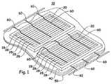
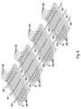
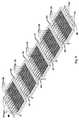
本発明は、図1〜5A−A及び7〜10に例示されているとおりの改良された光起電力セルアセンブリ10に関し、太陽放射(例えば、太陽光)を受けたときに電気エネルギーを提供するように機能する幾つかの部品のアセンブリとして一般に記載されうる。1つの例において、改良された光起電力セルアセンブリ10は、図6に示すようなソーラシングル(屋根板)100などの、より大きな光起電力デバイス中に取り込まれることができる。Detailed Description of the Preferred Embodiments The present invention relates to an improved
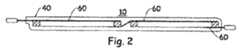
本開示の特に興味深く、主な焦点となっているのは、少なくとも複数の光起電力セル20、第一のカプセル化層及び第二のカプセル化層40、50、及び、光起電力セル20を電気接続している導電性要素60(好ましくは、複数の導電性要素60)を含む、改良された光起電力セルアセンブリ10である。 Of particular interest and main focus of the present disclosure is that at least a plurality of
一般に、複数の光起電力セルは複数の隣接する層から構成することができる。これらの層は(例えば、下から上に向かって)少なくとも:導電性基材層22、光活性層24及び上部電気回収構造28を含むものとさらに定めることができる。セルの周囲縁の一部分に少なくとも沿って、非導電性層部分30が、例えば、図4に示すとおりに含まれることも好ましい。 In general, a plurality of photovoltaic cells can be composed of a plurality of adjacent layers. These layers can be further defined as including at least: the
さらに、アセンブリ10は、導電性要素60の1つの末端62が回収構造28及び光活性層24の上面26の両方に接触しており、導電性要素60の反対側の末端64が隣接する光起電力セル20の導電性基材層22に接触しているように構成される。好ましくは、両末端62、64はそれぞれのカプセル化層によりセル層に接触している状態が維持される。 Further, the
部品及び部品アセンブリの関係(例えば、少なくとも1つの幾何学的特性及び材料特性)は上記の背景のセクションで議論した問題の1つ以上を解決するのに驚くほど重要であるものと考えられる。部品及び部品アセンブリの各々及びそれらの関係を以下のパラグラフでより詳細かつ明確に開示する。 The relationship between parts and part assemblies (eg, at least one geometrical and material property) is believed to be surprisingly important in solving one or more of the problems discussed in the background section above. Each of the parts and part assemblies and their relationships are disclosed in more detail and clearly in the following paragraphs.
本発明において考えられる光起電力セル20は任意の数の既知の市販の光起電力セルから作られてよく、又は、幾つかの将来的に開発される光起電力セルから選ばれてもよい。 The
導電性基材層22
導電性基材層22はそれが光活性部分により生成された電気エネルギーを伝導する点で、上部導電性層24と同様に機能する。導電性基材層22は剛性であっても又は可とう性であってもよいが、望ましくは可とう性であり、特に、得られる光起電力デバイスが非平面表面との組み合わせで使用されうる実施形態で可とう性である。導電性基材層は単一の一体の層であることができ、又は、1層以上の層から形成されることができ、その層は金属、合金、金属間化合物組成及び/又はこれらの組み合わせを含む、広範な材料から形成される。可とう性基材層が望まれる用途では、層22は、通常、金属ホイルである。例としては、Cu、Al、Ti、Mo又はステンレススチールを含む金属ホイルが挙げられる。通常、この導電性基材層はステンレススチールから形成され、光活性部分24は基材層の上に形成されるが、他の構成も考えられ、本明細書に示されるセル相互接続の概念に必ずしも影響を及ぼさない。例示の実施形態において、ステンレススチールは好ましい。Conductive
The
導電性基材層22は1つ以上のCu、Mo、Ag、Al、Cr、Ni、Ti、Ta、Nb、W及び/又はこれらの組み合わせを含む、広範な導電性材料で片面又は両面が被覆されてよい。Moを含む導電性組成物は例示の実施形態で使用されうる。光活性層に近位にある導電性基材層上に形成されている裏面接触層122は支持体から光活性層24を隔離するのを援助し、支持体構成成分が光活性層に移行するのを最少限にする。例えば、裏面接触層22はステンレススチール支持体のFe及びNi成分の光活性層24への移行をブロックするのを援助することができる。導電性基材層22の片面又は両面上に形成される導電性金属層は、また、光活性領域24の形成の間にS又はSeを使用するならばそれらから保護するなど、光活性層24の形成の間に生じうる劣化に対して基材層を保護することができる。
光活性部分24
光起電力セル20の光活性層又は部分24は光エネルギーを電気エネルギーに変換する材料を含む。その機能を提供することが知られている任意の材料は使用でき、その材料としては結晶性シリコン、非晶性シリコン、CdTe、GaAs、色素増感ソーラセル(いわゆるグラッチェルセル)、有機/ポリマーソーラセル、又は、光電効果により太陽光を電気に変換する任意のその他の材料が挙げられる。しかしながら、光活性セルは好ましくはIB−IIIA−カルコゲニド系セル、例えば、IB−IIIA−セレン化物、IB−IIIA−硫化物又はIB−IIIA−セレン化物硫化物(すなわち、吸収層はIB−IIIA−カルコゲニド、好ましくは銅カルコゲニドである)である。より特定的な例としては、銅インジウムセレニド、銅インジウムガリウムセレニド、銅ガリウムセレニド、銅インジウムスルフィド、銅インジウムガリウムスルフィド、銅ガリウムセレニド、銅インジウムスルフィドセレニド、銅ガリウムスルフィドセレニド及び銅インジウムガリウムスルフィドセレニド(そのすべてが本明細書中でCIGS呼ばれる)が挙げられる。これらはまた、式CuIn(1−x)GaxSe(2−y)Sy(式中、xは0〜1であり、yは0〜2である)により表すことができる。銅インジウムセレニド及び銅インジウムガリウムセレニドは好ましい。部分24は吸収層に加えて、複数の層を含むことができ、例えばCIGS系セルにおいて有用であることが当該技術分野で知られている、1つ以上のエミッタ(バッファ)層、導電性層(例えば、透明導電性層)などがここで考えられる。これらのセルは可とう性又は剛性であってよく、形状及びサイズがさまざまであることができるが、一般的に壊れやすく、環境劣化を受けやすい。好ましい実施形態では、光起電力セル20は実質的な亀裂及び/又は有意な機能損失なしに曲げることができるセルである。例示の光起電力セルはUS3767471、US4465575、US20050011550A1、EP841706A2、US20070256734a1、EP1032051A2、JP2216874、JP2143468及びJP10189924aを含む多くの米国特許及び刊行物中に教示されそして記載されており、それらの文献をすべての目的のために参照により本明細書に取り込む。
Photoactive layer or
例示の実施形態では、光活性層24は、さらに、任意の数の層から構成されてもよく、例えば、裏面接触層122(通常、Mo)、吸収層124(通常、CuInGaSe(S))、バッファ層126(通常、CdS)、ウィンドー層128(通常、ZnO)及び透明導電性層130(通常、インジウムスズオキシド(ITO)又はアルミニウム酸化亜鉛(AZO))である。この構成のセル20は、通常、「CIGSソーラセル」として知られているものと考えられる。図5A−Aを参照されたい。 In the illustrated embodiment, the
光起電力セル20は他の既知のソーラセル技術から形成され得るものと考えられる。これらの例としては、非晶性シリコン又はテルル化カドミウム系ソーラセルデバイスが挙げられる。さらに、上記のような光起電力セル20内の部品は代替材料で置き換えることができる。たとえば、バッファ層126は、Cd、Zn、In、Sn及びそれらの組み合わせの硫化物、セレン化物又は酸化物であることができる、Zn、Cd、In、Snなどの抵抗性透明酸化物を含む、任意要素であるウィンドー層は、バッファ領域126及び透明導電性層130との間に含まれることができる。好ましくは、ウィンドー層は真性酸化亜鉛である。 It is contemplated that the
透明導電性層130は光活性層24の上部層として配置されうる。広範な種類の透明導電性酸化物又はこれらの組み合わせを透明導電性層に組み込むことができる。典型的な実施形態では、透明導電性層130は透明導電性酸化物(TCO)であり、代表的な例としては、フッ素ドープ酸化スズ、酸化スズ、酸化インジウム、インジウムスズオキシド(ITO)、アルミニウムドープ酸化亜鉛(AZO)、酸化亜鉛、これらの組合せなどが挙げられる。1つの例示の実施形態では、透明導電性層はインジウムスズオキシドである。透明導電性層を、スパッタリング又は他の適切な堆積技術によって便利に形成することができる。 The transparent
ある光起電力セル20において、明確な透明導電性層130が必要とされないことがあるものと考えられる。例えば、GaAs層が十分な導電性であることができるので、GaAs型セルは、通常、透明導電体を必要としない。本発明のために、回収構造28の直下の層はセル20の上面26と考えられるべきである。 It is believed that in certain
これらの置換は当業者に知られており、本明細書で示されるセルの相互接続の概念に影響を与えない。 These permutations are known to those skilled in the art and do not affect the cell interconnect concept presented herein.
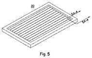
上部回収構造28
上部回収構造28は光活性部分22によって生成される電気エネルギーを収集し、導電性パスにそれを集中するように機能する。回収構造28は光活性層24の上(例えば、上面26上)に堆積させ、それにより、この層(例えば、TCO層130)のシート抵抗を低減することができる。回収構造28は、通常、光学的に不透明な材料を含み、また、実質的に平行な一連の導電体トレースとして適用されてもよく(他の構成が考えられ、必ずしもここに示されるセルの相互接続の概念に影響を及ぼさない)、トレース間の間隔は、グリッドが表面上で比較的小さな面積を占めるようにする。例えば、ある実施形態では、回収構造は、光活性材料を入射光に暴露させうるための光捕獲に関係する全表面積の約5%以下、さらには約2%以下、又は、さらには約1%以下を占める。回収構造28は、好ましくは、例えば、Ag、Al、Cu、Cr、Ni、Ti、Ta及び/又はそれらの組み合わせなどの導電性金属を含む。1つの例示の実施形態では、グリッドは、ニッケル及び銀を含む二層構造を有している。回収構造はスクリーン印刷、インクジェット印刷、電気メッキ及び蒸着又はスパッタリングなどの物理蒸着技術を使用してシャドウマスクを介して行う金属化を含む様々な技術によって形成することができる。
The
非導電性層部分30
非導電性層部分30はソーラセルの縁から導電性要素60を電気的に隔離するための絶縁体又は誘電体として機能する。非導電性層部分の存在は導電性要素60との接触により生じうるソーラセルの縁での電気的な短絡の発生を低減するものと考えられる。さらに、非導電性層部分30はカプセル化層の適用の前に、セルアセンブリの製造の間に複数の導電性要素60を適切に固定するための接着剤として機能することができる。絶縁体はソーラセルアセンブリ中の各々個々のソーラセルの前縁又は後縁の一方又は両方でソーラセル又は導電性要素60に適用されることができる。絶縁体は、導電性要素がソーラセルの縁を横切っている箇所で、デバイスの縁に沿って明確な領域として形成されることができ、又は、セル20の縁の全体の長さ又は実質的な部分に沿って単層として適用されることができ、それにより、セルと導電性要素60との間の明確な層を含むことができる。絶縁体は、液体として堆積され、そして硬化又は架橋して固体材料を形成することができる合成ポリマーのタイプであってよい。硬化又は架橋は、例えば、熱又は紫外線(UV)エネルギーの適用を介して達成することができる。UV硬化性組成物については、硬化プロセスを短時間で行うことができることが望ましく、例えば、10秒未満、より具体的には約3秒未満であることができる。多くの光硬化性ポリマーは、少なくとも300mJ/cm2のエネルギーを必要とし、より通常には、200〜400nmの範囲で約500〜1200mJ/cm2のUVエネルギーを必要とする。例示の実施形態としては、アクリレート及びエポキシ樹脂系組成物が挙げられる。あるいは、非導電性層部分30はテープの形態などの固体材料として適用することができる。適切な代替品としては、エチレンテトラフルオロエチレン(ETFE)などのフルオロカーボンポリマー、ソーラセル又は相互接続材料上に被覆されうる硬化性絶縁ポリマー、ソーラセル又は相互接続材料に適用することができる無機誘電性材料が挙げられる。また、ポリエチレンフィルムなどのカプセル化層40、50として使用される材料を置き換えることができると考えられる。好ましい実施形態では、非導電性層部分30は、紫外線により硬化される液体誘電性エポキシ組成物である。1つの例示の実施形態では、部分30はポリイミドテープである。1つのそのような市販のテープはDupont(登録商標)によって提供されるKapton(登録商標)テープである。一般に、非導電性層部分30は約2より大きい誘電率を示すことができ、さらには約4よりも大きくなることができる。例示の電気絶縁材料は、約4.8より大きい誘電率を有し、体積抵抗率は約3×1014Ω-cmよりも大きい。
導電性要素60
導電性要素60は光起電力セル20どうしの間の電気的なブリッジとして機能する。電気的ブリッジは、1つのセルの上部(例えば、回収構造28及び/又は上面26)と隣接するセルの導電性基材層26との間に形成されていることが本発明において考えられる。これらの要素は比較的に低い電気抵抗(好ましくは1.0Ω/m未満、より好ましくは約0.33Ω/m未満、最も好ましく0.15Ω/m未満)を有することが望ましい。図11はワイヤ抵抗率がセルアセンブリの直列抵抗及び正規化効率に与える効果の例を示す。それは従来の金属ワイヤ(中実又はメッキ)、導電性ホイル、被覆ポリマーストランドの形態、又は、上記のブリッジ機能を発揮する任意の同様の構造であることができる。例示の導電性要素としてはAg、Sn又はNiメッキされた銅ワイヤが挙げられる。要素60は比較的に低い融点(例えば、セルアセンブリの所望の加工温度よりも低い融点、通常、約200℃よりも低い融点)を有する合金、ハンダ又は導電性接着剤成分を含まない。
The
個々のセル当たりに使用される導電性要素60の数は2(例えば、上部及び底部に1つ)から数ダースで変更可能であるものと考えられる。導電性要素60の数及び相対間隔は多くの要因に基づいて変化することができ、その要因は、例えば、要素のタイプ及び抵抗率、セル20のサイズ、回収構造28中のラインのタイプ、抵抗率及び間隔、上面26のシート抵抗、回収構造28の個々の要素の間隔、及び、すべての関係する界面(例えば、回収構造/上面、回収構造/導電性要素、上面/導電性要素)の接触抵抗である。これらの値を各々測定して、総計の出力損失を最少化しそして導電性要素及び回収構造による遮蔽に関連する出力損失への寄与と関係する界面からの抵抗損失に対する寄与とをバランスさせるための好ましい構成を決定するために使用する。好ましい実施形態において、セル20の表面100cm2当たり4つの導電性要素60があり、これらは概ね均一に間隔を開けて離れている(例えば、間隔値は互いに約5〜25%の範囲内)。図12は出力損失(正規化効率)がどのようにして導電性要素の数を最適化することによって実験的に最少化されうるかの例を示している。It is contemplated that the number of
抵抗の目標(例えば、約1.0Ω未満、より好ましくは約2.0Ω未満)を満たすために、要素60と導電性基材層22との間に十分な接触がなされているべきであると考えられる。導電性基材層22に対する要素60のオーバーラップ「CA」(図4を参照されたい)は約2.0mmからセルの全幅(W)までの範囲とすることができるものと考えられる。好ましい実施形態において、オーバーラップ「CA」は約2.0mm〜100.0mmの範囲であり、より好ましくは約5.0mm〜80.0mmであり、最も好ましくは約20.0mm〜50.0mmである。There should be sufficient contact between the
導電性要素の数及び導電性要素の横断幅は、導電性要素の線抵抗及び導電性要素の遮蔽による合計出力損失が下記式
合計出力損失=[遮蔽による出力損失]+[抵抗線損失による出力損失]
=[{ρ(I/n)(l)/(V)(A)}]+[n(l’)(d)]The number of conductive elements and the transverse width of the conductive elements are the total output loss due to the line resistance of the conductive elements and the shielding of the conductive elements as follows: Total output loss = [output loss due to shielding] + [output due to resistance line loss] loss]
= [{Ρ (I / n) (l) / (V) (A)}] + [n (l ′) (d)]
(上式中、ρは導電性要素の抵抗率であり、IはPVデバイスにより発生される電流であり、nは導電性要素の数であり、lは導電性要素の長さであり、VはPVデバイスにより発生される電圧であり、Aは導電性要素の断面積であり、l’はPVセルの上面を覆っている導電性要素の長さであり、そしてdは導電性要素の直径である)によって3%未満〜6%となるように選択されうるものと考えられる。(Where ρ is the resistivity of the conductive element, I is the current generated by the PV device, n is the number of conductive elements, l is the length of the conductive elements, and V Is the voltage generated by the PV device, A is the cross-sectional area of the conductive element, l ′ is the length of the conductive element covering the top surface of the PV cell, and d is the diameter of the conductive element It is considered that the ratio can be selected to be less than 3% to 6%.
好ましい実施形態において、導電性要素の断面幅は約0.1mm〜2.0mmの範囲にあることができ、より好ましくは約0.2mm〜1.0mm、最も好ましくは約0.3mm〜0.5mmである。好ましい実施形態において、遮蔽により寄与される出力損失は遮蔽損失及び抵抗損失により生じる合計出力損失の約25〜75%であることができ、より好ましくは約30〜70%である。 In preferred embodiments, the cross-sectional width of the conductive element can be in the range of about 0.1 mm to 2.0 mm, more preferably about 0.2 mm to 1.0 mm, and most preferably about 0.3 mm to 0.00 mm. 5 mm. In a preferred embodiment, the power loss contributed by shielding can be about 25-75% of the total power loss caused by shielding loss and resistance loss, more preferably about 30-70%.
第一のカプセル化層40
第一のカプセル化層40が幾つかの機能を発揮することができるものと考えられる。例えば、層40は接合メカニズムとしての役割を果たすことができ、隣接する層(例えば、セル20、複数の導電性要素60及び/又は第二のカプセル化層50)を一緒に保持するのを助ける。また、所望の量及びタイプの光エネルギーが透過して、光起電力セル20(例えば、光活性部分24)に到達できるようにすべきである。第一カプセル化層40は、また、隣接する層の形状の不規則性を補償するように機能するか、又は、それらの層を変化(例えば、厚さの変化)させることができる。また、それは環境要因(例えば、温度変化、湿度など)ならびに物理的な運動及び曲げに起因する層間のたわみ及び運動を可能にする役割を果たすこともできる。好ましくは、層40は複数の導電性要素60を上面26及び回収構造28と電気接続させておくように構成される。好ましい実施形態では、第一のカプセル化層40は接着フィルム又はメッシュから本質的になることができるが、好ましくは、熱可塑性樹脂材料、例えば、EVA(エチレンビニルアセテート)、熱可塑性ポリオレフィン又は類似の材料である。層40は単層で構成されても、又は、複数層(第一、第二、第三、第四、第五層など)で構成されていてもよいものと考えられる。層40が複数の層を含む場合には、セルの上面の近位に形成される第一の層(例えば、上面26、上部電気回収構造28及び導電性要素60と接触している)は第一の層の近位に形成される第二の層よりも高い融解温度(Tm)を有することが考えられる。この構成では、熱処理の間に第一の層が完全に融解しないが、第一の層がセルの上部に付着するのに十分な温度に到達するように加工温度を選択することができるという利点を提供するものと考えられる。この構成は熱処理の間に導電性要素と上部導電性層との間にカプセル化材料が流れ落ちることによる上部導電性層と導電性要素の接触の損失を防止する。この層40の好ましい厚さは約0.1mm〜1.0mm、より好ましくは約0.2mm〜0.8mm、そして最も好ましくは約0.25mm〜0.5mmの範囲であることができる。多層構成では、層40は融解温度(Tm)の差異が少なくとも10℃である異なる層を含むべきであると考えられる。加工温度は第一の層のTmよりも約5℃以上低く、第二の層のTmよりも少なくとも5℃高いように選択されるべきである。例として、1つのこのような組み合わせは、融解温度105〜130℃の範囲であるポリオレフィン熱可塑性樹脂材料を含む第一の層、及び、公称融解温度が50℃〜100℃であるEVAコポリマータイプを含む第二の層であることができる。
It is believed that the
接触しているすべての表面に対するカプセル化層の吸着による「良好な」接着がカプセル化アセンブリの一体性を維持するために重要であるものと考えられる。一般的な指針として、ガラスへの吸着について測定される接着力は約20N/15mmを超え、より好ましくは約30N/15mmを超え、さらにより好ましくは約40N/15mmを超えるべきである。接着強度はASTM D903−98に記載されているとおりの標準180度の引張試験を用いて決定することができる。 It is believed that “good” adhesion by adsorption of the encapsulation layer to all contacting surfaces is important to maintain the integrity of the encapsulation assembly. As a general guide, the adhesion measured for adsorption to glass should be greater than about 20 N / 15 mm, more preferably greater than about 30 N / 15 mm, and even more preferably greater than about 40 N / 15 mm. Adhesive strength can be determined using a standard 180 degree tensile test as described in ASTM D903-98.
第二のカプセル化層50
カプセル化層の別の例において、第二のカプセル化層50は、一般に、光起電力セル20の下方に接続して配置されているが、ある場合には、第一のカプセル化層40に直接的に接触しうる。第二のカプセル化層50は第一のカプセル化層と同様の機能を発揮することができるが、必ずしも電磁線又は光エネルギーを透過させる必要はないものと考えられる。好ましくは、第二のカプセル化層50は複数の導電性要素60を導電性基材層22と電気接触させておくように構成される。層50が複数の層を含む場合には、セルの底面の近位に形成される第一の層(例えば、導電性基材層22及び導電性要素60と接触している)は第一の層の近位に形成される第二の層よりも高い融解温度(Tm)を有することが考えられる。この構成では、熱処理の間に第一の層が完全に融解しないが、第一の層がセルの底部に付着するのに十分な温度に到達するように加工温度を選択することができるという利点を提供するものと考えられる。この構成は熱処理の間に導電性要素と上部導電性層との間にカプセル化材料が流れ落ちることによる導電性基材層22と導電性要素の接触の損失を防止する。
In another example of the encapsulation layer, the
以下のパラグラフで、本発明の5つの実施例及び1つの比較例を示す。以下の実施例は本発明を例示するが、その範囲を限定しないことが意図される。 The following paragraphs show five examples of the present invention and one comparative example. The following examples illustrate the invention but are not intended to limit its scope.
実施例一般
これらの実施例の目的で、ステンレススチール基材(例えば、導電性基材層22)上のCIGS型ソーラセル(50mm×210mm)をGlobal Solar Inc.から入手する。セルをより小さいセル50mm(「L」)×25mm(「W」)に切断する。Ni/Agグリッド(例えば、回収構造28)をセルの上面26に、透明導電性層(ITO)上に適用する。この場合に、30本のラインはより長いセル寸法を横切って延在している。セル20をセルの縁付近でMo層(122)まで罫書く(例えば、外側縁から内側に向けて約1.0〜2.0mm)。このような罫書きの使用はセル20を切断することにより生じる損傷の理由から産業界で一般的であるものと信じられる。Examples General For the purposes of these examples, CIGS solar cells (50 mm × 210 mm) on stainless steel substrates (eg, conductive substrate layer 22) are obtained from Global Solar Inc. Cut the cell into
符号及び略記は本明細書中で以下のとおりに定義される。
Voc=電圧−開回路
Isc=電流−短絡
FF=曲線因子
Eff=効率
Rs=直列抵抗
Rsh=シャント(並列)抵抗
Rp=Rsh
Pmax=出力(ワット)
Jsc=電流−単位面積当たりの短絡(mA/cm2)The symbols and abbreviations are defined herein as follows.
Voc = voltage-open circuit Isc = current-short circuit FF = fill factor Eff = efficiency Rs = series resistance Rsh = shunt (parallel) resistance Rp = Rsh
Pmax = Output (Watt)
Jsc = current−short circuit per unit area (mA / cm2 )
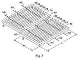
例1
図7に示すグリッドを有する2つのセルを4つの縁でポリイミド(kapton(登録商標))テープにより処理し(例えば、非導電性層部分30)、それにより、縁の周囲を覆い、そしてセルの上部で罫書きセクションを被覆した。3本のAg被覆ワイヤ(30AWG;例えば、導電性要素60)をセルAの表面に適用し、セルBの底面に延在させ、ここで、末端をkaptonテープを用いてステンレススチール基材に局所的に結合させた(カプセル化材40、50の適用の前)。同様にして、3本の30AWGのSn−被覆ワイヤをセルAの表面に適用し、そしてセル縁を超えて延在させた。ワイヤは、銀グリッドのフィンガーの方向と垂直の方向で適用した。セルの表面にワイヤを結合するために結合用材料を使用しなかった(しかしながら、テープの小片はラミネーションプロセスが起こることができるまで要素60を適切に固定するために使用された)。その後、セルAの底部ステンレススチール基材及びセルBを超えて延びているワイヤがクリップによる電気接続に利用可能なようにして、上面及び底面で400μmの厚さのDNP PV−FS Z68ポリエチレンシート(例えば、カプセル化剤40、50−図示せず)の間で2つのセルアセンブリをカプセル化した。DNP/ソーラセル/DNPアセンブリを、その後、150℃でラミネートした。セルA及びセルBの電流/電圧(I−V)特性データを個々に、また、相互接続されたアセンブリで図13に示す。Example 1
Two cells with the grid shown in FIG. 7 are treated with polyimide (kapton®) tape at four edges (eg, non-conductive layer portion 30), thereby covering the periphery of the edges and The scoring section was covered at the top. Three Ag-coated wires (30 AWG; eg, conductive element 60) are applied to the surface of cell A and extended to the bottom surface of cell B, where the ends are locally applied to the stainless steel substrate using kapton tape. (Before application of
例2
本例において、グリッドを含むセル20をさらに2つ調製し、例1の2つのセルに、図8に示すようにして追加した。それらのセルをセルC及びDと呼ぶことにする。これらのセルC及びDを互いに接続したものに関するデータを図13に要約する。セルアセンブリA+B及びC+Dを、その後、同一の方法を用いて互いに接続し、4セルストリングを製造した。Example 2
In this example, two
個々のセルA、B、C及びDならびに相互接続されたアセンブリに関するデータの要約を図13に示す。 A summary of the data for individual cells A, B, C and D and the interconnected assembly is shown in FIG.
例3
本例において、グリッドを含む5つのセル20を上記例と同様にして調製した。本例において、図9に示すように、10本のAgメッキCuワイヤ(30AWG;例えば、導電性要素60)を用いてトップツーボトム様式でセル20を組み立てる。ここでも、セルの表面にワイヤを結合するために結合用材料を使用しなかった。ワイヤが末端セルの縁を超えて延びているようにして、上面及び底面でDNP PV−FS Z68ポリエチレンシート片(カプセル化材40、50)の間でセル/要素60アセンブリをカプセル化する。その後、ワイヤ60をSn/Pbハンダを用いたハンダ付けによりSn−被覆Cuバスバー(「BB」)に結合する。DNP/ソーラセル/DNPアセンブリを、その後、110℃でラミネートする。電流/電圧(I−V)特性データを個々のセル及び相互接続されたアセンブリについて図14に示す。Example 3
In this example, five
例4
本例において、グリッドを含む5つのセル20を例3と同様に調製する。図9に示すように、トップツーボトム様式でセル20を組み立てるが、30AWGのAgメッキCuワイヤを28AWGのSn−被覆Cuワイヤ(要素60)で置き換える。電流/電圧(I−V)特性データを個々のセル及び相互接続されたアセンブリについて図15に示す。Example 4
In this example, five
例5
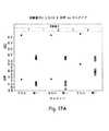
例3及び4と同様に、5セルアセンブリを3つ調製する。本例において、図11に示すように、グリッド設計はより大きなセル寸法を横切って広がる14本のラインを有し、トップツーボトム様式で、8本のSn−メッキCuワイヤ、28AWGを用いて組み立てる。I−V特性データを個々のセル及び相互接続されたアセンブリについて図17A−Cに示す。Example 5
Three 5-cell assemblies are prepared as in Examples 3 and 4. In this example, as shown in FIG. 11, the grid design has 14 lines extending across larger cell dimensions and is assembled using 8 Sn-plated Cu wires, 28AWG, in a top-to-bottom fashion. . IV characteristic data is shown in FIGS. 17A-C for individual cells and interconnected assemblies.
例6(比較例)
導電性エポキシを用いた従来のストリングアンドタブアプローチを用いて相互接続された5セルグローバルソーラアセンブリをI−V測定により特性化する。その後、セル間のリボンを切断することによりストリングを5つのセルに切断し、各セルについてI−V測定を行う。図16に要約するデータはストリングの性能が個々のセルよりも有意に低くなりうることを示す。それは本明細書に記載される方法により相互接続されたセルに対して得られるデータとは対照的である。Example 6 (comparative example)
A 5-cell global solar assembly interconnected using a conventional string and tab approach with conductive epoxy is characterized by IV measurements. Then, the string is cut into five cells by cutting the ribbon between the cells, and IV measurement is performed for each cell. The data summarized in FIG. 16 shows that string performance can be significantly lower than individual cells. It is in contrast to the data obtained for cells interconnected by the methods described herein.
例7(比較例)
導電性エポキシを用いた従来のストリングアンドタブアプローチを用いて相互接続された幾つかの5セルグローバルソーラアセンブリをI−V測定により特性化した。その後、例6で記載したようにセル間のリボンを切断することによりストリングを5つのセルに切断した。8本の30AWGで例3に記載したアプローチを用いて5つのセルをストリングへと再組み立てし、各セルについてI−V測定を行う。図16に要約するデータはストリングの性能が個々のセルよりも有意に低くなりうることを示す。それは本明細書に記載される方法により相互接続されたセルに対して得られるデータとは対照的である。Example 7 (comparative example)
Several 5-cell global solar assemblies interconnected using a conventional string and tab approach using conductive epoxy were characterized by IV measurements. The string was then cut into five cells by cutting the ribbon between the cells as described in Example 6. Five 30 AWGs are reassembled into a string using the approach described in Example 3 and IV measurements are made for each cell. The data summarized in FIG. 16 shows that string performance can be significantly lower than individual cells. It is in contrast to the data obtained for cells interconnected by the methods described herein.
方法
光起電力セル20をアセンブリ10へと組み立てる方法も発明性があると考えられる。上記のすべての部品を提供し、アセンブリ10を製造するために使用される組み立て方法は少なくとも下記のことを含むものと考えられる。Method The method of assembling the
第一の工程は各光起電力セルの上面26に複数の導電性要素60を適用することを含む。ソーラセル20はバッチ又はスタック内に設けられ、手動又は自動でアンローディングステーションに提供されることができる。ソーラセル20は、あるいは、複数のソーラセルを含む連続ロールの形で提供され、単体化と呼ばれる工程で組み立て直前にロールから分離されうる。単体化されたソーラセル20は光起電力性能により分類された容器(ビン)に提供することができる。ビンに提供されたセルは手動でオペレータが個別にロードすることができる。又は、より好ましくは、産業用ロボットを用いてビンから個々のセルを取り上げ、検査領域に配置することができる。その後、視覚システムを用いて、光起電力セルを高精度でピックアップし、そして適切な向きでフラットトップ真空コンベヤ上に配置するように産業用ロボットを導くことができる。1つの実施形態では、視覚システムは、セルの上面の画像を撮るカメラを含み、それはロボットに対してセルの正確な向きに関する情報を伝え、それにより、ロボットはセルを取り上げ、それを正確に位置決めされた向きでコンベヤ上に配置する。 The first step involves applying a plurality of
セル20を、その後、コンベアに沿って移動させ、その間に、非導電性層部分30を熱もしくはUV硬化性液体誘電体として又はテープの形態でセルの一方又は両方の縁の付近に適用することができる。もし非導電性層がテープの形態で適用されるならば、テープはセルの上面26と複数の導電性要素60との両方に接触するように接着面が利用可能となるように両面上に接着剤を含むタイプのものが好ましい。
非導電性層部分30を有するセルをコンベヤで下流に輸送していくときに、複数の導電性要素60を連続形態で上面26に適用することができる。複数の導電性要素は非導電性層部分の接着特性を用いて両方の周囲縁でセルの上面に固定されうる。もし非導電性層部分が両面接着テープであるならば、複数の導電性要素をテープ上で接着剤により適切な位置に配置することが援助されうる。もし非導電性層部分がUV硬化性液体誘電体であるならば、複数の導電性要素は非導電性層部分の中に部分的に埋め込まれてよい。その後、液体誘電体を硬化して、セルの上面に両方の周囲縁にて導電性要素を固定することができる。 As the cells having
上記の方法は、上面26に接触している複数の導電性要素を含むセルの連続「ストリング」を製造する。セルは十分なギャップにより分離されており、それにより、各セルの後方周囲縁を超えて所望の長さの導電性要素が延びていることができる。この長さは仕上がり製品中の導電性基材層22上の要素60の所望のオーバーラップ「CA」により定義される。その後、複数の導電性要素を各ソーラセルの前縁で切断し、複数の導電性要素が上面26に接触しておりそしてソーラセルの後縁を超えて延びている個々のセルを製造することができる。切断方法はニップの使用などの機械操作により行うことができ、又は、レーザを使用して、特定の位置でワイヤを切断するなどして行うことができる。The above method produces a continuous “string” of cells that includes a plurality of conductive elements in contact with the
セルの「ストリング」を製造すると同時に、バス又は端子バーの同様の「ストリング」を同様にして製造することができ、ここで、複数の導電性要素を溶接又はハンダ付けにより複数の端子バーに結合させる。好ましい実施形態において、この方法はレーザ溶接により行われる。導電性要素を切断し、複数の導電性要素が結合されそして後縁方向に延びている単一の端子バーを製造する。 At the same time that a cell “string” is manufactured, a similar “string” of bus or terminal bar can be manufactured in the same way, where multiple conductive elements are bonded to multiple terminal bars by welding or soldering. Let In a preferred embodiment, this method is performed by laser welding. The conductive elements are cut to produce a single terminal bar in which a plurality of conductive elements are combined and extend in the trailing edge direction.
ソーラセルにおいて導電性要素を切断し、そして端子バープロセスを行った後に、導電性要素が結合されている端子バーをピックアンドプレースメカニズムにより相互接続領域に輸送することができる。相互接続領域は第二のカプセル化材50を保持するための留め具を含むことができる。端子バーは適当な位置に固定されうる。その後、後縁を超えて延びている導電性要素を有するセルを第二のカプセル化層の上に配置することができ、それにより、端子バーの後縁を超えて延びている複数の導電性要素は第一のソーラセルの裏側に接触する。第二のセルを、その後、配置し、それにより、第一のセルの後縁を超えて延びている複数の導電性要素は第二のセルの裏側に接触する。所望の数のセルが相互接続アセンブリ中に配置されるまでこのプロセスを繰り返す。その後、導電性要素が結合していない第二の端子バーを第二のカプセル化材の上で適当な位置に配置する。最後のセルの後縁を超えて延びている導電性要素はハンダ付け又は溶接を用いて第二の端子バーに結合される。好ましい実施形態において、このプロセスはレーザ溶接により行われる。 After cutting the conductive element in the solar cell and performing the terminal bar process, the terminal bar to which the conductive element is coupled can be transported to the interconnect region by a pick and place mechanism. The interconnect region can include a fastener for holding the
向かい合った端部で端子バーを取り付けられた、相互接続されたアセンブリの完了に続いて、第一のカプセル化材40を相互接続されたアセンブリの上部の上に配置することができる。第一のカプセル化層、ソーラセル、複数の導電性要素及び端子バーを含む製品を、例えば、真空ラミネーター中で積層し、このようにしてアセンブリ10を完成する。 Following completion of the interconnected assembly with terminal bars attached at opposite ends, a
特に断らない限り、本明細書中に記載した種々の構造の寸法及び幾何形状は本発明を限定することを意図せず、他の寸法又は幾何形状は可能である。複数の構造部品は単一の統合された構造により提供されうる。あるいは、単一の統合された構造は別々の複数の部品に分割されうる。さらに、本発明の特徴は例示された実施形態の1つだけの文脈で説明されている可能性があるが、そのような特徴は、任意の所与の用途で、他の実施形態の1つ以上の他の特徴と組み合わされてよい。また、本明細書中の独特の構造の製造及びその操作は本発明による方法を構成することは上記から理解されるであろう。 Unless otherwise noted, the dimensions and geometry of the various structures described herein are not intended to limit the invention, and other dimensions or geometries are possible. Multiple structural parts can be provided by a single integrated structure. Alternatively, a single integrated structure can be divided into separate parts. Moreover, while features of the invention may be described in the context of only one illustrated embodiment, such features may be considered one of the other embodiments for any given application. It may be combined with other features described above. It will also be appreciated from the above that the manufacture and operation of the unique structure herein constitutes a method according to the present invention.
本発明の好適な実施形態を開示してきた。しかしながら、当業者は、特定の変更は本発明の教示の範囲内になるであろうことが判るであろう。それゆえ、以下の特許請求の範囲は本発明の真の範囲及び内容を決定するために検討されるべきである。 A preferred embodiment of the present invention has been disclosed. However, one of ordinary skill in the art appreciates that certain modifications will be within the scope of the teachings of the invention. Therefore, the following claims should be studied to determine the true scope and content of this invention.
上記出願で引用した任意の数値は、任意のより低い値と任意のより高い値との間に少なくとも2単位の隔たりがある場合には、1単位の増分で、より低い値からより高い値までのすべての数値を含む。成分の量、又は、温度、圧力及び時間などのプロセス変数の値が、例えば、1〜90、好ましくは20〜80、より好ましくは30〜70であると記載されるならば、15〜85、22〜68、43〜51、30〜32などの値は本明細書中に明確に列挙されていることが意図される。1未満である値に関しては、1単位は0.0001、0.001、0.01又は0.1であると適宜考えられる。これらは特に意図されたものの例に過ぎず、列挙された下限値及び上限値の間の数値のすべての可能な組み合わせは本願中で同様に明確に記載されたものと考えられるべきである。 Any numerical value quoted in the above application is from a lower value to a higher value in 1 unit increments if there is at least a 2 unit gap between any lower value and any higher value. Includes all numbers. If the amount of components or the value of process variables such as temperature, pressure and time is described as, for example, 1 to 90, preferably 20 to 80, more preferably 30 to 70, 15 to 85, Values such as 22-68, 43-51, 30-32, etc. are intended to be explicitly listed herein. For values that are less than 1, one unit is considered to be 0.0001, 0.001, 0.01, or 0.1 as appropriate. These are merely examples of what is specifically intended and all possible combinations of numerical values between the listed lower and upper limits should be considered as clearly described herein as well.
特に断りのないかぎり、すべての範囲は両末端及びその末端の間のすべての数値を含む。範囲の関係で「約」又は「およそ」を使用すると、その範囲の両末端に適用される。このように、「約20〜30」は少なくとも特定した末端を含んで「約20〜約30」を網羅する。 Unless otherwise noted, all ranges include both numbers and all numerical values between the ends. Use of “about” or “approximately” in relation to a range applies to both ends of the range. Thus, “about 20-30” covers “about 20 to about 30” including at least the specified ends.
特許出願及び公開を含むすべての論文及び文献の開示はすべての目的で参照により本明細書中に取り込む。 The disclosures of all articles and references, including patent applications and publications, are incorporated herein by reference for all purposes.
組み合わせを記載する用語「から本質的になる(consisting essentially of)」は特定される要素、成分、部品又は工程、及び、組み合わせの基本的かつ新規の特徴に実質的に影響を及ぼさないような他の要素、成分、部品又は工程を含む。 The term “consisting essentially of” describing a combination refers to the specified element, component, part or process, and others that do not substantially affect the basic and novel characteristics of the combination. Element, component, part or process.
要素、成分、部品又は工程の組み合わせを記載する用語「含む(comprising)」又は「含む(including)」の使用は、要素、成分、部品又は工程から本質的なる実施形態をも考慮している。 The use of the term “comprising” or “including” to describe a combination of elements, components, parts or steps also contemplates embodiments that consist essentially of the elements, components, parts or steps.
複数の要素、成分、部品又は工程は単一の統合された要素、成分、部品又は工程により提供されてよい。あるいは、単一の統合された要素、成分、部品又は工程は別個の複数の要素、成分、部品又は工程に分割されてよい。要素、成分、部品又は工程を記載するための「a」又は「one」は追加の要素、成分、部品又は工程を排除することを意図しない。特定の族に属する元素又は金属に関するすべての記載はCRC Press Inc.により出版されそして著作権が与えられている元素の周期律表を参照する。族についての記載は属の番号付けのためのIUPACシステムを使用してこの元素の周期律表に反映された族に対してなされる。
要素番号のリスト
光起電力セルアセンブリ10
光起電力セル20
導電性基材層22
光活性層24
上面26
回収構造28
非導電性層部分30
第一のカプセル化層40
第二のカプセル化層50
導電性要素60
導電性要素60の1つの末端62
導電性要素60の反対側の末端64
裏面接触層122
CuInGaSe(S)の吸収層124
バッファ層126
ウィンドー層128
透明導電性層130Multiple elements, components, parts or steps may be provided by a single integrated element, component, part or process. Alternatively, a single integrated element, component, part or process may be divided into separate multiple elements, components, parts or processes. “A” or “one” to describe an element, component, part or process is not intended to exclude an additional element, component, part or process. All descriptions relating to elements or metals belonging to a particular group can be found in CRC Press Inc. Refer to the periodic table of elements published and copyrighted by. The group description is made for the group reflected in the periodic table of this element using the IUPAC system for genus numbering.
List of Element Numbers
Conductive
One end 62 of the
Opposite end 64 of
Back
CuInGaSe (S)
Transparent
Claims (9)
Translated fromJapanese反対側導電性基材層と、
の間に挟まれた光活性部分を含む、複数の光起電力セルであって、セルの周囲縁部分の少なくとも一部分は非導電性層部分を含む、複数の光起電力セル、
複数の導電性要素、
前記上部回収構造及び光活性部分の露出上面と接触している第一のカプセル化層、及び、
前記反対側導電性基材層と接触している第二のカプセル化層、
を含み、
前記複数の導電性要素の1つの末端は前記上部回収構造及び露出上面と接触しており、前記複数の導電性要素の反対側末端は隣接する光起電力セルの導電性基材層と接触しており、両方の末端はそれぞれのカプセル化層によりセル層への接触を維持している、光起電力セルアセンブリ。An upperrecovery structure on a partial area of the upper surface of the photoactive portion, leaving an exposed upper surface in other areas;
An opposite conductive substrate layer;
A plurality of photovoltaic cells including a photoactive portion sandwiched therebetween, wherein at least a portion of a peripheral edge portion of the cell includes a non-conductive layer portion;
A plurality of conductive elements,
A first encapsulation layer in contact with the upperrecovery structure and the exposed upper surface of the photoactive portion; and
A second encapsulation layer in contact with the opposite conductive substrate layer;
Including
One end of the plurality of conductive elements is in contact with the upperrecovery structure and the exposed top surface, and the opposite end of the plurality of conductive elements is in contact with a conductive substrate layer of an adjacent photovoltaic cell. A photovoltaic cell assembly, wherein both ends maintain contact to the cell layer by respective encapsulation layers.
一連の実質的に平行な導電性要素を提供すること、
光活性層、反対側導電性基材層、及び、透明導電性層と回収構造との両方を含む上部導電性層を含む、複数の光起電力セルを提供すること、
トップツーボトム様式で複数の光起電力セルを接続すること、
の工程を含む、光起電力アセンブリの形成方法であって、
前記回収構造は一連の実質的に平行なラインを含み、セルの周囲縁部分は非導電性層部分を含み、複数の導電性要素の1つの末端は透明導電性層及び回収構造の両方に接触しており、複数の導電性要素の反対側末端は隣接する光起電力セルの導電性基材層に接触しており、両末端はそれぞれのカプセル化層によりセル層に接触した状態を維持している、方法。Providing a first encapsulation layer and a second encapsulation layer;
Providing a series of substantially parallel conductive elements;
Providing a plurality of photovoltaic cells comprising a photoactive layer, an opposite conductive substrate layer, and an upper conductive layer comprising both a transparent conductive layer and a recovery structure;
Connecting multiple photovoltaic cells in a top-to-bottom manner,
A method of forming a photovoltaic assembly comprising the steps of:
The recovery structure includes a series of substantially parallel lines, the peripheral edge portion of the cell includes a non-conductive layer portion, and one end of the plurality of conductive elements contacts both the transparent conductive layer and the recovery structure. The opposite ends of the plurality of conductive elements are in contact with the conductive substrate layer of the adjacent photovoltaic cell, and both ends are kept in contact with the cell layer by the respective encapsulation layers. Is that way.
Applications Claiming Priority (3)
| Application Number | Priority Date | Filing Date | Title |
|---|---|---|---|
| US38386710P | 2010-09-17 | 2010-09-17 | |
| US61/383,867 | 2010-09-17 | ||
| PCT/US2011/051509WO2012037191A2 (en) | 2010-09-17 | 2011-09-14 | Improved photovoltaic cell assembly and method |
Publications (2)
| Publication Number | Publication Date |
|---|---|
| JP2013541205A JP2013541205A (en) | 2013-11-07 |
| JP5629010B2true JP5629010B2 (en) | 2014-11-19 |
Family
ID=44674927
Family Applications (1)
| Application Number | Title | Priority Date | Filing Date |
|---|---|---|---|
| JP2013529278AExpired - Fee RelatedJP5629010B2 (en) | 2010-09-17 | 2011-09-14 | Improved photovoltaic cell assembly and method |
Country Status (5)
| Country | Link |
|---|---|
| US (1) | US20130167910A1 (en) |
| EP (1) | EP2617065A2 (en) |
| JP (1) | JP5629010B2 (en) |
| CN (1) | CN103109378B (en) |
| WO (1) | WO2012037191A2 (en) |
Families Citing this family (24)
| Publication number | Priority date | Publication date | Assignee | Title |
|---|---|---|---|---|
| CN104272128B (en)* | 2012-05-29 | 2016-11-09 | 优信电子(香港)有限公司 | Solar power generation monitoring method and solar power generation monitoring system used in the method |
| CN104335356B (en)* | 2012-05-31 | 2016-11-09 | 陶氏环球技术有限责任公司 | High Utilization Photovoltaic Devices |
| JP2014175520A (en)* | 2013-03-11 | 2014-09-22 | Mitsubishi Electric Corp | Solar battery module and manufacturing method for the same |
| WO2015199857A1 (en) | 2014-06-26 | 2015-12-30 | Dow Global Technologies Llc | Photovoltaic devices with sealant layer and laminate assembly for improved wet insulation resistance |
| US20160035907A1 (en)* | 2014-08-04 | 2016-02-04 | Lg Electronics Inc. | Solar cell module |
| EP3373341B1 (en)* | 2014-09-30 | 2019-09-18 | LG Electronics Inc. | Solar cell |
| US10056522B2 (en) | 2014-12-05 | 2018-08-21 | Solarcity Corporation | System and apparatus for precision automation of tab attachment for fabrications of solar panels |
| US9899546B2 (en) | 2014-12-05 | 2018-02-20 | Tesla, Inc. | Photovoltaic cells with electrodes adapted to house conductive paste |
| DE102014225631A1 (en)* | 2014-12-11 | 2016-06-16 | Osram Gmbh | Photovoltaic module and photovoltaic system |
| US11532765B2 (en)* | 2015-04-30 | 2022-12-20 | Shangrao Jinko Solar Technology Development Co., Ltd | Solar cell and solar cell panel including the same |
| JP5860183B1 (en)* | 2015-05-26 | 2016-02-16 | トヤマキカイ株式会社 | Conductive tape applicator |
| WO2017000599A1 (en)* | 2015-07-02 | 2017-01-05 | 苏州阿特斯阳光电力科技有限公司 | Solar cell module |
| US10586882B2 (en)* | 2015-11-17 | 2020-03-10 | Lg Electronics Inc. | Solar cell panel, and apparatus and method for attaching interconnector of solar cell panel |
| CN105489689B (en)* | 2016-02-02 | 2017-05-10 | 浙江晶科能源有限公司 | A kind of photovoltaic module and method for making photovoltaic module |
| KR101823605B1 (en)* | 2016-12-02 | 2018-03-14 | 엘지전자 주식회사 | Solar cell and solar cell panel including the same |
| CN106847967B (en)* | 2016-12-28 | 2018-08-10 | 珠海格力电器股份有限公司 | Photovoltaic module and packaging method thereof |
| FR3087298A1 (en)* | 2018-10-16 | 2020-04-17 | Voltinov Voltaique Innovation | IMPROVED SOLAR MODULE |
| EP3963676A4 (en)* | 2019-05-02 | 2022-12-28 | NewSouth Innovations Pty Limited | METHOD OF FORMING A DEVICE STRUCTURE |
| EP3764406A1 (en)* | 2019-07-11 | 2021-01-13 | Oxford Photovoltaics Limited | Multi-junction photovoltaic device |
| CN116960207A (en)* | 2021-03-05 | 2023-10-27 | 浙江晶科能源有限公司 | Cell string structure and photovoltaic module and manufacturing method thereof |
| JP2023080413A (en)* | 2021-11-30 | 2023-06-09 | 株式会社カネカ | Solar cell panel, solar cell module, and method for manufacturing solar cell panel |
| CN114709284B (en)* | 2022-03-31 | 2023-03-24 | 盐城百佳年代薄膜科技有限公司 | Photovoltaic cell assembly with EVA (ethylene-vinyl acetate) adhesive film reflection structure |
| CN115241295A (en)* | 2022-07-21 | 2022-10-25 | 常州时创能源股份有限公司 | Photovoltaic cell unit and application thereof |
| US11923473B1 (en)* | 2022-12-06 | 2024-03-05 | Maxeon Solar Pte. Ltd. | Shingled solar module with ribbon interconnect |
Family Cites Families (31)
| Publication number | Priority date | Publication date | Assignee | Title |
|---|---|---|---|---|
| US3767471A (en) | 1971-09-01 | 1973-10-23 | Bell Telephone Labor Inc | Group i-iii-vi semiconductors |
| US4465575A (en) | 1981-09-21 | 1984-08-14 | Atlantic Richfield Company | Method for forming photovoltaic cells employing multinary semiconductor films |
| JPH02143468A (en) | 1988-11-24 | 1990-06-01 | Mitsubishi Electric Corp | Solar cell |
| JPH02216874A (en) | 1989-02-17 | 1990-08-29 | Hitachi Ltd | Silicon crystalline solar cell |
| US6331673B1 (en)* | 1995-10-17 | 2001-12-18 | Canon Kabushiki Kaisha | Solar cell module having a surface side covering material with a specific nonwoven glass fiber member |
| JP3527815B2 (en) | 1996-11-08 | 2004-05-17 | 昭和シェル石油株式会社 | Method for producing transparent conductive film of thin film solar cell |
| JP3501606B2 (en) | 1996-12-27 | 2004-03-02 | キヤノン株式会社 | Method for manufacturing semiconductor substrate and method for manufacturing solar cell |
| JP2000312019A (en)* | 1999-02-25 | 2000-11-07 | Canon Inc | Photovoltaic module array, photovoltaic module array installation structure, photovoltaic module installation method, and photovoltaic power generation system |
| JP3056200B1 (en) | 1999-02-26 | 2000-06-26 | 鐘淵化学工業株式会社 | Method of manufacturing thin film photoelectric conversion device |
| US8076568B2 (en)* | 2006-04-13 | 2011-12-13 | Daniel Luch | Collector grid and interconnect structures for photovoltaic arrays and modules |
| US7022910B2 (en) | 2002-03-29 | 2006-04-04 | Konarka Technologies, Inc. | Photovoltaic cells utilizing mesh electrodes |
| JP3872306B2 (en)* | 2001-02-01 | 2007-01-24 | 信越半導体株式会社 | Solar cell module and method for installing solar cell module |
| JP2003069055A (en)* | 2001-06-13 | 2003-03-07 | Sharp Corp | Solar cell and method of manufacturing the same |
| CN1643629A (en) | 2002-01-25 | 2005-07-20 | 科纳卡科技有限公司 | Structures and materials for photovoltaic cell |
| US20070251570A1 (en) | 2002-03-29 | 2007-11-01 | Konarka Technologies, Inc. | Photovoltaic cells utilizing mesh electrodes |
| US7619159B1 (en)* | 2002-05-17 | 2009-11-17 | Ugur Ortabasi | Integrating sphere photovoltaic receiver (powersphere) for laser light to electric power conversion |
| DE10239845C1 (en) | 2002-08-29 | 2003-12-24 | Day4 Energy Inc | Electrode for photovoltaic cells, photovoltaic cell and photovoltaic module |
| US6938761B2 (en) | 2003-06-10 | 2005-09-06 | J&M Innovative Products, Llc | Sportsmen's utility bucket cover apparatus and method |
| CN100481524C (en)* | 2003-09-10 | 2009-04-22 | 大日本印刷株式会社 | Encapsulant layer for solar battery assembly and solar battery assembly |
| JPWO2006104107A1 (en)* | 2005-03-29 | 2008-09-11 | 京セラ株式会社 | Polycrystalline silicon substrate and manufacturing method thereof, polycrystalline silicon ingot, photoelectric conversion element, and photoelectric conversion module |
| JP2006278710A (en)* | 2005-03-29 | 2006-10-12 | Kyocera Corp | Solar cell module and manufacturing method thereof |
| US20070204900A1 (en)* | 2006-03-02 | 2007-09-06 | Li-Hung Lai | Package structure for a solar chip |
| JP4663664B2 (en)* | 2006-03-30 | 2011-04-06 | 三洋電機株式会社 | Solar cell module |
| US20070256734A1 (en) | 2006-05-08 | 2007-11-08 | United Solar Ovonic Llc | Stabilized photovoltaic device and methods for its manufacture |
| US20080128018A1 (en)* | 2006-12-04 | 2008-06-05 | Richard Allen Hayes | Solar cells which include the use of certain poly(vinyl butyral)/film bilayer encapsulant layers with a low blocking tendency and a simplified process to produce thereof |
| EP2100336A4 (en)* | 2006-12-22 | 2013-04-10 | Applied Materials Inc | INTERCONNECTION TECHNOLOGIES FOR REAR CONTACT SOLAR CELLS AND MODULES |
| JP5384004B2 (en)* | 2007-03-19 | 2014-01-08 | 三洋電機株式会社 | Solar cell module |
| US8697980B2 (en)* | 2007-06-19 | 2014-04-15 | Hanergy Holding Group Ltd. | Photovoltaic module utilizing an integrated flex circuit and incorporating a bypass diode |
| US8299350B2 (en)* | 2007-08-02 | 2012-10-30 | Sanyo Electric Co., Ltd. | Solar cell module and method for manufacturing the same |
| US20090255565A1 (en) | 2008-01-31 | 2009-10-15 | Global Solar Energy, Inc. | Thin film solar cell string |
| FR2930556B1 (en)* | 2008-04-28 | 2012-08-17 | Arkema France | COMPOSITION BASED ON POLYAMIDE GRAFT POLYMER AND USE THEREOF IN PHOTOVOLTAIC MODULES |
- 2011
- 2011-09-14JPJP2013529278Apatent/JP5629010B2/ennot_activeExpired - Fee Related
- 2011-09-14EPEP11760665.7Apatent/EP2617065A2/ennot_activeWithdrawn
- 2011-09-14CNCN201180044936.9Apatent/CN103109378B/ennot_activeExpired - Fee Related
- 2011-09-14USUS13/820,647patent/US20130167910A1/ennot_activeAbandoned
- 2011-09-14WOPCT/US2011/051509patent/WO2012037191A2/enactiveApplication Filing
Also Published As
| Publication number | Publication date |
|---|---|
| WO2012037191A2 (en) | 2012-03-22 |
| JP2013541205A (en) | 2013-11-07 |
| CN103109378A (en) | 2013-05-15 |
| EP2617065A2 (en) | 2013-07-24 |
| WO2012037191A3 (en) | 2012-09-13 |
| CN103109378B (en) | 2016-06-01 |
| US20130167910A1 (en) | 2013-07-04 |
Similar Documents
| Publication | Publication Date | Title |
|---|---|---|
| JP5629010B2 (en) | Improved photovoltaic cell assembly and method | |
| JP6082046B2 (en) | Improved photovoltaic cell assembly | |
| TWI429093B (en) | Solar battery module | |
| US9385254B2 (en) | Integrated thin film solar cell interconnection | |
| US20170288078A1 (en) | Interconnect assembly | |
| JP6550042B2 (en) | Solar cell module and method of manufacturing the same | |
| EP2400561A2 (en) | Photovoltaic module | |
| EP2950352A2 (en) | Photovoltaic cell interconnect | |
| EP2761674B1 (en) | Photovoltaic cell interconnect | |
| US20140102532A1 (en) | Solar cell module, method for manufacturing solar cell module, and tab wire for thin film solar cells | |
| EP2789019B1 (en) | A photovoltaic article comprising a photovoltaic cell with electrical connection elements |
Legal Events
| Date | Code | Title | Description |
|---|---|---|---|
| A131 | Notification of reasons for refusal | Free format text:JAPANESE INTERMEDIATE CODE: A131 Effective date:20140218 | |
| A977 | Report on retrieval | Free format text:JAPANESE INTERMEDIATE CODE: A971007 Effective date:20140219 | |
| A521 | Request for written amendment filed | Free format text:JAPANESE INTERMEDIATE CODE: A523 Effective date:20140514 | |
| TRDD | Decision of grant or rejection written | ||
| A01 | Written decision to grant a patent or to grant a registration (utility model) | Free format text:JAPANESE INTERMEDIATE CODE: A01 Effective date:20140902 | |
| A61 | First payment of annual fees (during grant procedure) | Free format text:JAPANESE INTERMEDIATE CODE: A61 Effective date:20141002 | |
| R150 | Certificate of patent or registration of utility model | Ref document number:5629010 Country of ref document:JP Free format text:JAPANESE INTERMEDIATE CODE: R150 | |
| R250 | Receipt of annual fees | Free format text:JAPANESE INTERMEDIATE CODE: R250 | |
| R250 | Receipt of annual fees | Free format text:JAPANESE INTERMEDIATE CODE: R250 | |
| LAPS | Cancellation because of no payment of annual fees |