JP5619540B2 - Charger - Google Patents
ChargerDownload PDFInfo
- Publication number
- JP5619540B2 JP5619540B2JP2010199806AJP2010199806AJP5619540B2JP 5619540 B2JP5619540 B2JP 5619540B2JP 2010199806 AJP2010199806 AJP 2010199806AJP 2010199806 AJP2010199806 AJP 2010199806AJP 5619540 B2JP5619540 B2JP 5619540B2
- Authority
- JP
- Japan
- Prior art keywords
- potential
- nmos
- unit
- secondary battery
- current
- Prior art date
- Legal status (The legal status is an assumption and is not a legal conclusion. Google has not performed a legal analysis and makes no representation as to the accuracy of the status listed.)
- Active
Links
- 238000001514detection methodMethods0.000claimsdescription20
- 230000002265preventionEffects0.000claimsdescription19
- 230000005669field effectEffects0.000claimsdescription10
- 230000000903blocking effectEffects0.000claimsdescription6
- 238000007599dischargingMethods0.000claimsdescription3
- 238000011144upstream manufacturingMethods0.000claimsdescription3
- 238000000034methodMethods0.000description10
- 238000010586diagramMethods0.000description8
- 239000004065semiconductorSubstances0.000description7
- 238000012986modificationMethods0.000description6
- 230000004048modificationEffects0.000description6
- 239000003990capacitorSubstances0.000description1
- 230000007423decreaseEffects0.000description1
- 230000003247decreasing effectEffects0.000description1
- 230000000694effectsEffects0.000description1
Images


Classifications
- H—ELECTRICITY
- H02—GENERATION; CONVERSION OR DISTRIBUTION OF ELECTRIC POWER
- H02J—CIRCUIT ARRANGEMENTS OR SYSTEMS FOR SUPPLYING OR DISTRIBUTING ELECTRIC POWER; SYSTEMS FOR STORING ELECTRIC ENERGY
- H02J7/00—Circuit arrangements for charging or depolarising batteries or for supplying loads from batteries
- H02J7/34—Parallel operation in networks using both storage and other DC sources, e.g. providing buffering
- H02J7/35—Parallel operation in networks using both storage and other DC sources, e.g. providing buffering with light sensitive cells
- H—ELECTRICITY
- H02—GENERATION; CONVERSION OR DISTRIBUTION OF ELECTRIC POWER
- H02J—CIRCUIT ARRANGEMENTS OR SYSTEMS FOR SUPPLYING OR DISTRIBUTING ELECTRIC POWER; SYSTEMS FOR STORING ELECTRIC ENERGY
- H02J7/00—Circuit arrangements for charging or depolarising batteries or for supplying loads from batteries
- H02J7/0029—Circuit arrangements for charging or depolarising batteries or for supplying loads from batteries with safety or protection devices or circuits
- H02J7/0031—Circuit arrangements for charging or depolarising batteries or for supplying loads from batteries with safety or protection devices or circuits using battery or load disconnect circuits
- H—ELECTRICITY
- H02—GENERATION; CONVERSION OR DISTRIBUTION OF ELECTRIC POWER
- H02J—CIRCUIT ARRANGEMENTS OR SYSTEMS FOR SUPPLYING OR DISTRIBUTING ELECTRIC POWER; SYSTEMS FOR STORING ELECTRIC ENERGY
- H02J7/00—Circuit arrangements for charging or depolarising batteries or for supplying loads from batteries
- H02J7/0029—Circuit arrangements for charging or depolarising batteries or for supplying loads from batteries with safety or protection devices or circuits
- H02J7/00302—Overcharge protection
Landscapes
- Engineering & Computer Science (AREA)
- Power Engineering (AREA)
- Charge And Discharge Circuits For Batteries Or The Like (AREA)
- Secondary Cells (AREA)
Description
Translated fromJapanese本発明は、二次電池の過充電を防止する充電装置に関する。 The present invention relates to a charging device that prevents overcharge of a secondary battery.
充電を行うことにより電池として繰り返し使用可能ないわゆる二次電池(蓄電池、充電式電池とも称する)を充電する場合には、二次電池の破壊や損傷を防ぐための過充電対策が従来よりなされている。例えば特許文献1には、太陽電池に並列に接続されたNチャンネル形のパワーMOSFETを、バッテリ(二次電池)の端子間電圧が所定値以上となったときにオンして、太陽電池からのバッテリへの充電電流を遮断することにより、バッテリの過充電を防止する装置が開示されている。 When charging a so-called secondary battery (also referred to as a storage battery or a rechargeable battery) that can be used repeatedly as a battery by charging, an overcharge countermeasure has been taken to prevent the secondary battery from being destroyed or damaged. Yes. For example, in
ところで、近年、二次電池の種類が増加しており、セル電圧が互いに異なる複数の二次電池を1つのシステムで用いる場合もある。このようなシステムでは、アプリケーションの種別やシステムの動作状況に応じて二次電池を適宜切り替えて使用するので、二次電池のそれぞれのセル電圧に対応できる充電装置が必要とされる。複数のセル電圧に対応できる回路を構成しようとすると、回路面積の増加や消費電流の増加が問題となる。例えば高いセル電圧に対応できる回路を構成する場合には降圧回路の降圧値を大きくすれば良いが、小電流で降圧値を大きくするためには降圧回路を構成するトランジスタのゲート長を大きくする必要があるので回路面積が大きくなってしまう。また、トランジスタのゲート長を大きくせずに降圧値を大きくするためには電流値を大きくする必要があるので、消費電流が増加してしまう。 By the way, in recent years, the types of secondary batteries are increasing, and a plurality of secondary batteries having different cell voltages may be used in one system. In such a system, since the secondary battery is appropriately switched and used according to the type of application and the operation status of the system, a charging device that can correspond to each cell voltage of the secondary battery is required. When a circuit that can handle a plurality of cell voltages is to be constructed, an increase in circuit area and an increase in current consumption are problematic. For example, when configuring a circuit that can handle a high cell voltage, it is sufficient to increase the step-down value of the step-down circuit, but in order to increase the step-down value with a small current, it is necessary to increase the gate length of the transistors constituting the step-down circuit As a result, the circuit area becomes large. Further, in order to increase the step-down value without increasing the gate length of the transistor, it is necessary to increase the current value, so that the current consumption increases.
本発明は上記した如き問題点に鑑みてなされたものであって、回路面積や消費電流を増加させることなく、複数のセル電圧に対応して過充電を防止することができる充電装置を提供することを目的とする。 The present invention has been made in view of the above-described problems, and provides a charging device capable of preventing overcharge corresponding to a plurality of cell voltages without increasing the circuit area and current consumption. For the purpose.
本発明による充電装置は、入力される充電電流を逆流防止部を介して二次電池へ供給する充電装置であって、二次電池の充電可能電圧に応じて決定される選択信号に応じて少なくとも2つの判定電位のうちの1つを選択して当該選択した判定電位と前記逆流防止部の下流の電位に基づく比較電位とを比較して満充電状態を検出する比較検出部と、前記比較検出部が満充電状態を検出したときに前記逆流防止部への前記充電電流の供給を遮断する遮断部と、を含み、前記比較検出部は、前記逆流防止部の上流の電位と基準電位との間に共通の定電流源を介して接続された基準電流枝路及び少なくとも2つの判定電流枝路と、前記判定電流枝路の1つを選択する選択部と、を含み、前記基準電流枝路は、前記基準電位に接続されたゲートを有する第1の電界効果トランジスタにおけるソース及びドレイン間の電流路を含み、前記判定電流枝路の各々は、前記比較電位に接続されたゲートを有する第2の電界効果トランジスタにおけるソース及びドレイン間の電流路と、これに直列に接続され且つ前記選択部によって選択されたときにオンするスイッチと、を含み、前記第2の電界効果トランジスタの各々におけるソース及びドレイン間の導通を開始させるゲート電圧は互いに異なることを特徴とする。A charging device according to the present invention is a charging device that supplies an input charging current to a secondary battery via a backflow prevention unit, and at least according to a selection signal determined according to a chargeable voltage of the secondary battery. A comparison detection unit that selects one of the two determination potentials and compares the selected determination potential with a comparison potential based on a potential downstream of the backflow prevention unit to detect a fully charged state; and the comparison detection partseen including and a blocking portion for blocking the supply of the charging current to the backflow prevention unit when detects a fully chargedstate, the comparison detection unit, upstream of the potential of the backflow prevention unit and the reference potential A reference current branch and at least two determination current branches connected via a common constant current source, and a selection unit for selecting one of the determination current branches, the reference current branch The path has a gate connected to the reference potential A current path between the source and drain in one field effect transistor, each of the decision current branches being a current path between the source and drain in a second field effect transistor having a gate connected to the comparison potential And a switch connected in series and turned on when selected by the selection unit, and the gate voltages for starting conduction between the source and the drain in each of the second field effect transistors are different from each other It is characterized by.
本発明による充電装置によれば、回路面積や消費電流を増加させることなく、複数のセル電圧に対応して過充電を防止することができる。 According to the charging device of the present invention, overcharging can be prevented in correspondence with a plurality of cell voltages without increasing the circuit area and current consumption.
以下、本発明に係る実施例について添付の図面を参照しつつ詳細に説明する。
<第1の実施例>
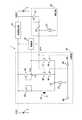
図1は本実施例の充電装置1の構成を太陽電池2及び二次電池3と共に示すブロック図である。充電装置1は、充電電流供給源である太陽電池2から入力端子81に入力された充電電流の逆流を防止しつつ、出力端子82に接続された二次電池3へ当該充電電流を供する充電装置であり、二次電池3の過充電を防止する機能をも備えた充電装置である。充電装置1は、逆流防止部10と、降圧部20と、放電部30と、比較部40と、を含む。Hereinafter, embodiments according to the present invention will be described in detail with reference to the accompanying drawings.
<First embodiment>
FIG. 1 is a block diagram showing the configuration of the
逆流防止部10は、二次電池3から太陽電池2への電流の逆流を防止する回路である。以下、逆流防止部10の太陽電池2の側を上流、逆流防止部10の二次電池3の側を下流と称する。 The
降圧部20は、二次電池3の端子電位VBATから例えば1Vなどの所定電位だけ降下させて降圧電位posを生成し、これを比較部40に供給する回路である。比較部40が正常な比較処理を行えるように、比較部40の動作電位よりも低い電位(降圧電位pos)を比較部40に供給するものである。以下、降圧電位posを比較電位posとも称する。 The step-down
降圧部20は、PMOSトランジスタ21と、抵抗22と、定電流源23と、からなる。PMOSトランジスタ21のソースは二次電池3に接続され、ドレインは抵抗22の一端に接続され、ゲートはドレインに接続されている。抵抗22の一端は定電流源23に接続され、他端はPMOSトランジスタ21のドレインに接続されている。抵抗22の当該一端の電位が降圧電位posとして比較部40に供給される。 The step-down
放電部30は、比較部40からの出力電位outが例えばローレベル等の所定の電位である場合に、太陽電池2から出力された充電電流を接地電位へ放電する回路である。これによって、二次電池3への充電電流を遮断して二次電池3の過充電を防止することができる。以下、放電部30を遮断部30とも称する。 The
比較部40は、降圧部20から供給された降圧電位posと、自身が生成した判定電位とを比較し、比較結果に対応する出力電位outを放電部30に供給する。 The
比較部40は、定電流源41と、デプレッション型NMOSトランジスタ(以下、DMOSと称する)42と、エンハンス型PMOSトランジスタ(以下、PMOSと称する)43及び44と、エンハンス型NMOSトランジスタ(以下、NMOSと称する)45乃至48と、選択信号入力端子49と、インバータ50と、を含む。 The
定電流源41と、DMOS42と、PMOS43及び44と、NMOS45乃至48とにより、差動の比較回路が構成されている。詳細には以下のように構成されている。 The constant
定電流源41の一端は基準電位(gnd)に接続され、他端はノードn1においてDMOS42のソースに接続されている。 One end of the constant
DMOS42のソースはノードn1において定電流源41に接続され、ゲートは接地電位に接続され、ドレインはPMOS43のドレインに接続されている。このように、DMOS42はソースフォロワ接続されている。PMOS43のソースは太陽電池2に接続され、ゲートはドレインに接続され、ドレインはDMOS42のドレインに接続されている。このように、DMOS42とPMOS43とは直列に接続されている。以下、DMOS42とPMOS43とが直列に接続されてなる電流路を基準電流枝路と称する。基準電流枝路は、DMOS42のソース−ドレイン路を含んでいる。 The source of the
PMOS44のソースは太陽電池2に接続され、ゲートはドレインに接続され、ドレインはノードn2においてNMOS45のドレインに接続されている。NMOS45のソースはNMOS46のドレインに接続され、ゲートは降圧部20の出力(抵抗22の一端)に接続され、ドレインはノードn2においてPMOS44のドレインに接続されている。NMOS46のソースはノードn1において定電流源41に接続され、ゲートは選択信号入力端子49に接続され、ドレインはNMOS45のソースに接続されている。このように、PMOS44とNMOS45とNMOS46とは直列に接続されている。以下、PMOS44とNMOS45とNMOS46とが直列に接続されてなる電流路を第1の判定電流枝路と称する。第1の判定電流枝路は、NMOS45のソース−ドレイン路を含んでいる。 The source of the
NMOS47のソースはNMOS48のドレインに接続され、ゲートは降圧部20の出力(抵抗22の一端)に接続され、ドレインはノードn2においてPMOS44のドレインに接続されている。NMOS48のソースは定電流源41に接続され、ゲートはインバータ50を介して選択信号入力端子49に接続され、ドレインはNMOS47のソースに接続されている。このように、PMOS44とNMOS47とNMOS48とは直列に接続されている。以下、PMOS44とNMOS47とNMOS48とが直列に接続されてなる電流路を第2の判定電流枝路と称する。第2の判定電流枝路は、NMOS47のソース−ドレイン路を含んでいる。また、第1の判定電流枝路と第2の判定電流枝路とは並列に接続されている。 The source of the
選択信号入力端子49には、NMOS46及びNMOS48のいずれか一方をオンするための選択信号が入力される。NMOS46及びNMOS48の各々は選択信号によってオン/オフするスイッチである。NMOS46のゲートには選択信号が直接入力され、NMOS48のゲートにはインバータ50を介して選択信号が入力される。選択信号がハイレベルの場合にはNMOS46がオンし、選択信号がローレベルの場合にはNMOS48がオンする。このように、NMOS46はNMOS45及びNMOS47のうちのNMOS45の側を選択するためのスイッチとして動作し、NMOS48はNMOS47を選択するためのスイッチとして動作する。以下、選択信号入力端子49とインバータ50からなる構成を選択部とも称する。 A selection signal for turning on one of the
このように構成された比較部40による比較結果を示すノードn2の電位が出力電位outとして放電部30に供給される。 The potential of the node n2 indicating the comparison result by the
充電装置1の動作について以下に説明する。ここで、DMOS42の閾値電圧をVtd、NMOS45の閾値電圧をVt45、NMOS47の閾値電圧をVt47とし、Vt47がVt45よりも大きい場合の例について説明する。閾値電圧は、ソース−ドレイン間の導通を開始させるゲート電圧である。 The operation of the
DMOS42はソースフォロワ接続されているので、DMOS42のソースが接続されているノードn1の電位は−Vtdとなる。Vtdが例えば−0.6Vの場合、ノードn1の電位は0.6Vとなる。 Since the
選択信号入力端子49にハイレベルの選択信号を入力した場合には、NMOS46がオンし、NMOS48がオフする。これによって、NMOS45及びNMOS47のうちのNMOS45が選択され、NMOS45のソースにはノードn1の電位である−Vtd(例えば0.6V)が供給される。 When a high level selection signal is input to the selection
したがって、降圧部20からNMOS45のゲートに供給される降圧電位posが、ノードn1の電位である−VtdとNMOS45の閾値Vt45との和以上になった場合に、NMOS45がオンする。当該和によって得られた電位が、放電処理を行うか否かを判定するための判定電位Vjである。 Therefore, when the step-down potential pos supplied from the step-down
Vtdが例えば−0.6V、Vt45が例えば0.7Vの場合、判定電位Vjは1.3V(=0.7V+{−(−0.6V)})となる。降圧電位posが判定電位Vjである1.3V以上になったときにNMOS45がオンする。判定電位Vjは、DMOS42の閾値Vtdの絶対値とNMOS45の閾値Vt45との和としても考えられる。 When Vtd is, for example, −0.6 V and Vt45 is, for example, 0.7 V, the determination potential Vj is 1.3 V (= 0.7 V + {− (− 0.6 V)}). The
NMOS45がオンすると、ノードn2の電位である出力電位outがローレベルになる。ローレベルの出力電位outは放電部30に供給され、放電部30は太陽電池2からの充電電流を接地電位へ放電する。なお、NMOS45がオフ状態のときには出力電位outはハイレベルであり、放電部30は放電をしていない。 When the
かかる動作により、降圧電位posが判定電位Vjである1.3V以上になったときに、放電処理がなされるので、二次電池3が過充電されるのを防止することができる。 With this operation, the discharge process is performed when the step-down potential pos is equal to or higher than the determination potential Vj of 1.3 V, so that the
選択信号入力端子49にローレベルの選択信号を入力した場合には、NMOS48がオンし、NMOS46がオフする。これによって、NMOS45及びNMOS47のうちのNMOS47が選択され、NMOS47のソースにはノードn1の電位である−Vtd(例えば0.6V)が供給される。 When a low level selection signal is input to the selection
したがって、降圧部20からNMOS47のゲートに供給される降圧電位posが、ノードn1の電位である−Vtdと、NMOS47の閾値Vt47との和以上になった場合に、NMOS47がオンする。当該和によって得られた電位が、放電処理を行うか否かを判定するための判定電位Vjである。 Accordingly, when the step-down potential pos supplied from the step-down
Vtdが例えば−0.6V、Vt47が例えば1.0Vの場合、判定電位Vjは1.6V(=1.0V+{−(−0.6V)})となる。降圧電位posが判定電位Vjである1.6V以上になったときにNMOS47がオンする。 For example, when Vtd is −0.6 V and Vt47 is 1.0 V, for example, the determination potential Vj is 1.6 V (= 1.0 V + {− (− 0.6 V)}). The
NMOS47がオンすると、ノードn2の電位である出力電位outがローレベルになる。ローレベルの出力電位outは放電部30に供給され、放電部30は太陽電池2からの充電電流を接地電位へ放電する。 When the
かかる動作により、降圧電位posが判定電位Vjである1.6V以上になったときに、放電処理がなされるので、二次電池3が過充電されるのを防止することができる。 With this operation, the discharge process is performed when the step-down potential pos becomes 1.6 V or more, which is the determination potential Vj, so that the
このように、選択信号入力端子49にロー及びハイのいずれか一方のレベルの信号を入力することによって、放電処理を行うか否かを判定するための判定電位Vjを選択することができる。上記した例の場合には、1.3Vと1.6Vのいずれかを判定電位Vjとして選択することができる。 In this way, by inputting a signal of one of the low level and the high level to the selection
上記したように、本実施例の充電装置1によれば、閾値電圧が互いに異なる2つのNMOSトランジスタのうちの1つを選択することにより、放電処理を行うか否かを判定するための判定電位Vjを2つの電位のうちから選択することができるので、セル電圧が互いに異なる2種類の二次電池に対応した過充電防止処理を行うことができる。かかる構成とすることにより、降圧部における降圧値を従来よりも増加させる必要がなく、回路面積の増加も抑制できる。 As described above, according to the
図2は、充電装置1を含む半導体チップ100、太陽電池2及び二次電池3がプリント基板200に搭載されたシステム構成を示すブロック図である。 FIG. 2 is a block diagram illustrating a system configuration in which the
充電装置1は、LSIなどの半導体チップ100の一部として構成することができる。半導体チップ100、太陽電池2及び二次電池3は例えばプリント基板200に搭載される。半導体チップ100内には二次電池3の種別を判別しその種別に応じた選択信号S1を充電装置1へ通知する制御部110が設けられている。充電装置1においては、選択信号S1の信号レベルに応じて判定電位Vjが選択される。選択信号入力端子49(図1)への選択信号S1の入力は、半導体チップ100の外部から供給するようにしても良い。
<第1の実施例の変形例>
図3は、本実施例の充電装置1の構成を示すブロック図である。以下、第1の実施例と異なる部分について主に説明する。本実施例の充電装置1は、比較的大容量の二次電池3(第1の供給先)と比較的小容量の二次電池4(第2の供給先)についての過充電を防止しつつ、二次電池3と二次電池4との間で充電電流の供給先を切り替えながら充電するものである。充電装置1は、切替部79を含む。切替部79の構成について以下に説明する。The charging
<Modification of the first embodiment>
FIG. 3 is a block diagram illustrating a configuration of the
VDD電位検出部80の入力は、VDDに接続され、その出力はインバータ82と2OR84に接続されると共に、比較部40のlo入力に接続される。VDD2電位検出部81の入力は、VDD2に接続され、その出力は2OR83と2OR84に接続される。インバータ82の出力は、2OR83の入力に接続される。 An input of the VDD
PMOS70のドレインは、逆流防止部10を介して太陽電池2に接続され、ゲートはインバータ60の出力に接続され、ソースは二次電池4に接続されている。PMOS70のゲートにはインバータ60を介して2OR83の出力が入力される。 The drain of the
PMOS71のソースは、逆流防止部10を介して太陽電池2に接続され、ゲートはPMOS73及びNMOS74からなるインバータ75の出力に接続され、ドレインはPMOS72のドレインに接続されている。PMOS72のドレインは、PMOS71のドレインに接続され、ゲートはPMOS76及びNMOS77からなるインバータ78の出力に接続され、ソースは二次電池3に接続されている。このように、PMOS71とPMOS72とは直列に接続されている。インバータ75及びインバータ78の各々には、2OR84の出力が入力される。 The source of the
なお、PMOS71乃至72からなる構成については、1つのPMOSで構成することもできるが、上記のような構成とすることにより、二次電池4の充電電圧VDDが二次電池3の充電電圧VDD2よりも小さい場合でも、VDD2からVDDへ電流が流れないという効果を奏する。
二次電池3の充電電圧VDD2が所定の値より低い場合、VDD2電位検出部81の出力はローレベルとなり、PMOS70と、PMOS71及びPMOS72は、VDD電位検出部80の出力で制御される。
この状態で、二次電池4の充電電圧VDDが所定の値より低い場合、VDD電位検出部80の出力はローレベルとなり、PMOS70がオンし、PMOS71及びPMOS72がオフする。二次電池4の充電電圧VDDが所定の値より高い場合、VDD電位検出部80の出力はハイレベルとなり、PMOS70がオフし、PMOS71及びPMOS72がオンする。つまり、VDD電位検出部80の出力レベルに応じて、二次電池3及び二次電池4のいずれか一方が選択的に充電される。
二次電池3の充電電圧VDD2が所定の値より高い場合、VDD2電位検出部81の出力はハイレベルとなり、VDD電位検出部80の出力によらず、PMOS70と、PMOS71及びPMOS72が全てオンし、二次電池3及び二次電池4が同時に充電される。Note that the configuration composed of the
When the charging voltage VDD2 of the
In this state, when the charging voltage VDD of the secondary battery 4 is lower than a predetermined value, the output of the VDD
When the charging voltage VDD2 of the
図4は、充電装置1における二次電池4の充電電圧VDD及び二次電池3の充電電圧VDD2電圧と、VDD電位検出部80及びVDD2電位検出部81の出力と、インバータ82の出力と、2OR83及び84の出力とを示すタイムチャートである。以下、図4を参照しつつ、充電装置1の動作について説明する。 FIG. 4 shows the charging voltage VDD of the secondary battery 4 and the charging voltage VDD2 voltage of the
ここで、DMOS42の閾値電圧をVtd、NMOS45の閾値電圧をVt45、NMOS47の閾値電圧をVt47とし、Vt47がVt45よりも大きい場合の例について説明する。また、二次電池4は二次電池3と比較し、容量は小さいが耐圧は高い二次電池である。 Here, an example in which the threshold voltage of the
充電開始時刻である時刻T0においては、二次電池3及び二次電池4が十分に充電されておらず、VDD電位検出部80及びVDD2電位検出部81の出力は共にローレベルである。インバータ82の出力はハイレベルとなり、2OR83の出力もハイレベルとなりPMOS70がオン、2OR84の出力がローレベルとなりPMOS71及びPMOS72がオフするので、二次電池4が充電される。二次電池4の充電電圧は図4にVDDとして示される。
NMOS48もオンするが、降圧電位posが判定電位Vjよりも小さい。ゆえに、NMOS47がオフ状態となるので、比較部40からの出力電位outはハイレベルであり、放電部30は放電しない。At time T0, which is the charging start time, the
The
VDD電位検出部80の出力がローレベルのときには、NMOS48がオンし、NMOS46がオフしている。つまり、閾値電圧が比較的高いNMOS47の側が選択されているので、判定電位Vjが高く設定されている。この場合の判定電位Vjは例えば1.6V(=1.0V+{−(−0.6V)})である。 When the output of the VDD
二次電池4が徐々に充電され、時刻T1においてその電圧値VDDがVHに達すると、VDD電位検出部80の出力がハイレベルとなり、インバータ82の出力はローレベルとなり、2OR83の出力もローレベルとなりPMOS70がオフ、2OR84の出力がハイレベルとなりPMOS71及びPMOS72がオンするので、二次電池3が充電される。二次電池3の充電電圧は図4にVDD2として示される。
NMOS46もオンするが、降圧電位posが判定電位Vjよりも小さい。ゆえに、NMOS45がオフ状態となるので、比較部40からの出力電位outはハイレベルであり、放電部30は放電しない。
VDD電位検出部80の出力がハイレベルのときには、NMOS46がオンし、NMOS48がオフしている。つまり、閾値電圧が比較的低いNMOS45の側が選択されているので、判定電位Vjが低く設定されている。この場合の判定電位Vjは例えば1.3V(=0.7V+{−(−0.6V)})である。
二次電池3が徐々に充電され、その間に二次電池4に充電された電荷がVDDを電源としたシステムの電流消費により徐々に放電され、時刻T2においてその電圧値VDDがVLに達すると、VDD電位検出部80の出力がローレベルとなり、インバータ82の出力はハイレベルとなり、2OR83の出力もハイレベルとなりPMOS70がオン、2OR84の出力がローレベルとなりPMOS71及びPMOS72がオフするので、二次電池4が充電される。
NMOS48もオンするが、降圧電位posが判定電位Vjよりも小さい。ゆえに、NMOS47がオフ状態となるので、比較部40からの出力電位outはハイレベルであり、放電部30は放電しない。When the secondary battery 4 is gradually charged and its voltage value VDD reaches VH at time T1, the output of the VDD
The
When the output of the VDD
When the
The
時刻T2以降も上記したのと同様の動作を繰り返す。かかる動作により、比較的小容量の二次電池4は充放電を繰り返し、比較的大容量の二次電池3は徐々に充電される。 The same operation as described above is repeated after time T2. With this operation, the secondary battery 4 having a relatively small capacity is repeatedly charged and discharged, and the
二次電池3の電圧がVDD2電位検出部81のしきい値VFに達すると、VDD2電位検出部81の出力はハイレベルになり、VDD電位検出部80の出力によらず2OR83および2OR84の出力がハイレベルになる。PMOS70とPMOS71及びPMOS72が共にオンし、二次電池3と二次電池4が同時に充電される。 When the voltage of the
二次電池3と二次電池4が同時に充電され続け、二次電池4の電圧値VDDがVHに達すると、VDD電位検出部80の出力がハイレベルとなり、NMOS46がオンする。
更に二次電池3と二次電池4の充電が進み、二次電池4の電圧値VDDがVC1に達すると、降圧部20からの降圧電位posが判定電位Vjより大きくなり、比較部40からの出力電位outはローレベルとなり、放電部30は放電し、二次電池4の電圧値VDDがVC1の電位で安定する。
二次電池4の充電電圧VDDの電位レベルに応じて充電先を二次電池3と二次電池4との間で相互に切り替えるのに連動して、判定電位Vjの値も切り替えている。
ここで、降圧部20の降圧電位pos+比較部40のNMOS47が選択された場合の判定電位Vjの和が、VDD電位検出部80のハイ側しきい値VHより高くなるようNMOS47のしきい値Vt47を設定すれば、二次電池4の充電電圧VDDをVHとVLと(図4)の間で増減させつつ、放電部30で充電電流を放電させる事なく二次電池3を徐々に充電できる。
このように、本実施例の充電装置1は、過充電を防止しつつ、2つの二次電池3及び4の間で充電先を切り替えながら充電する。比較的小容量の二次電池4は充電開始から短時間で充電されるので、システムを早期に立ち上げるための電源として利用できる。しかし、二次電池4をシステムの初期動作のための電源として利用した場合には、その電圧VDDが低下するので、二次電池4を電源として利用している期間中に比較的大容量の二次電池3を充電する。このように、比較的小容量の二次電池4をシステムの初期動作のための電源として利用しつつ、比較的大容量の二次電池3を徐々に充電し、二次電池3が十分に充電された後に二次電池3をシステムの通常動作時の電源として利用できる。充電装置1のかかる構成により、システムの早期動作と通常動作時の安定動作とを実現できる。
<第2の実施例>
図5は本実施例の充電装置1の構成を太陽電池2及び二次電池3と共に示すブロック図である。以下、第1の実施例と異なる部分について主に説明する。本実施例の充電装置1は、図1に示される選択信号入力端子49及びインバータ50を含まず、比較部40内にNMOS51及び52、選択信号入力端子53乃至55を含む。When the
When the
The value of the determination potential Vj is also switched in conjunction with the mutual switching of the charging destination between the
Here, the threshold value Vt47 of the
Thus, the charging
<Second embodiment>
FIG. 5 is a block diagram showing the configuration of the
NMOS46のゲートは選択信号入力端子53に接続されている。NMOS48のゲートは選択信号入力端子54に接続されている。NMOS45乃至48についてのその他の接続は第1の実施例と同じである。 The gate of the
NMOS51のソースはNMOS52のドレインに接続され、ゲートは降圧部20の出力(抵抗22の一端)に接続され、ドレインはノードn2においてPMOS44のドレインに接続されている。NMOS52のソースはノードn1において定電流源41に接続され、ゲートは選択信号入力端子55に接続され、ドレインはNMOS51のソースに接続されている。このように、PMOS44とNMOS51とNMOS52とは直列に接続されている。以下、PMOS44とNMOS51とNMOS52とが直列に接続されてなる電流路を第3の判定電流枝路と称する。第3の判定電流枝路は、NMOS51のソース−ドレイン路を含んでいる。 The source of the
充電装置1の動作について以下に説明する。ここで、DMOS42の閾値電圧をVtd、NMOS45の閾値電圧をVt45、NMOS47の閾値電圧をVt47、NMOS51の閾値電圧をVt51とし、Vt51がVt47よりも大きく、Vt47がVt45よりも大きい場合の例について説明する。 The operation of the
DMOS42はソースフォロワ接続されているので、DMOS42のソースが接続されているノードn1の電位は−Vtdとなる。Vtdが例えば−0.6Vの場合、ノードn1の電位は0.6Vとなる。 Since the
選択信号入力端子53乃至55のうちの53のみにハイレベルの選択信号を入力した場合には、NMOS46がオンし、NMOS48及び52がオフする。これによって、NMOS45、47及び51のうちのNMOS45が選択され、NMOS45のソースにはノードn1の電位である−Vtd(例えば0.6V)が供給される。 When a high level selection signal is input only to 53 of the selection signal input terminals 53 to 55, the
したがって、降圧部20からNMOS45のゲートに供給される降圧電位posが、ノードn1の電位である−Vtdと、NMOS45の閾値Vt45との和によって得られる判定電位Vj以上になった場合に、NMOS45がオンする。 Therefore, when the step-down potential pos supplied from the step-down
Vtdが例えば−0.6V、Vt45が例えば0.7Vの場合、判定電位Vjは1.3V(=0.7V+{−(−0.6V)})となる。降圧電位posが判定電位Vjである1.3V以上になったときにNMOS45がオンする。 When Vtd is, for example, −0.6 V and Vt45 is, for example, 0.7 V, the determination potential Vj is 1.3 V (= 0.7 V + {− (− 0.6 V)}). The
NMOS45がオンすると、ノードn2の電位である出力電位outがローレベルになる。ローレベルの出力電位outは放電部30に供給され、放電部30は太陽電池2からの充電電流を接地電位へ放電する。 When the
かかる動作により、降圧電位posが判定電位Vjである1.3V以上になったときに、放電処理がなされるので、二次電池3が過充電されるのを防止することができる。 With this operation, the discharge process is performed when the step-down potential pos is equal to or higher than the determination potential Vj of 1.3 V, so that the
選択信号入力端子53乃至55のうちの54のみにハイレベルの選択信号を入力した場合には、NMOS48がオンし、NMOS46及び52がオフする。これによって、NMOS45、47及び51のうちのNMOS47が選択され、NMOS47のソースにはノードn1の電位である−Vtd(例えば0.6V)が供給される。 When a high level selection signal is input only to 54 of the selection signal input terminals 53 to 55, the
したがって、降圧部20からNMOS47のゲートに供給される降圧電位posが、ノードn1の電位である−Vtdと、NMOS47の閾値Vt47との和によって得られる判定電位Vj以上になった場合に、NMOS47がオンする。 Accordingly, when the step-down potential pos supplied from the step-down
Vtdが例えば−0.6V、Vt45が例えば1.0Vの場合、判定電位Vjは1.6V(=1.0V+{−(−0.6V)})となる。降圧電位posが判定電位Vjである1.6V以上になったときにNMOS47がオンする。 For example, when Vtd is −0.6 V and Vt45 is 1.0 V, for example, the determination potential Vj is 1.6 V (= 1.0 V + {− (− 0.6 V)}). The
NMOS47がオンすると、ノードn2の電位である出力電位outがローレベルになる。ローレベルの出力電位outは放電部30に供給され、放電部30は太陽電池2からの充電電流を接地電位へ放電する。 When the
かかる動作により、降圧電位posが判定電位Vjである1.6V以上になったときに、放電処理がなされるので、二次電池3が過充電されるのを防止することができる。 With this operation, the discharge process is performed when the step-down potential pos becomes 1.6 V or more, which is the determination potential Vj, so that the
選択信号入力端子53乃至55のうちの55のみにハイレベルの選択信号を入力した場合には、NMOS52がオンし、NMOS46及び48がオフする。これによって、NMOS45、47及び51のうちのNMOS51が選択され、NMOS51のソースにはノードn1の電位である−Vtd(例えば0.6V)が供給される。 When a high level selection signal is input to only 55 of the selection signal input terminals 53 to 55, the
したがって、降圧部20からNMOS51のゲートに供給される降圧電位posが、ノードn1の電位である−Vtdと、NMOS51の閾値Vt51との和によって得られる判定電位Vj以上になった場合に、NMOS51がオンする。 Accordingly, when the step-down potential pos supplied from the step-down
Vtdが例えば−0.6V、Vt51が例えば1.5Vの場合、判定電位Vjは2.1V(=1.5V+{−(−0.6V)})となる。降圧電位posが判定電位Vjである2.1V以上になったときにNMOS51がオンする。 For example, when Vtd is −0.6 V and Vt51 is 1.5 V, for example, the determination potential Vj is 2.1 V (= 1.5 V + {− (− 0.6 V)}). The
NMOS51がオンすると、ノードn2の電位である出力電位outがローレベルになる。ローレベルの出力電位outは放電部30に供給され、放電部30は太陽電池2からの充電電流を接地電位へ放電する。 When the
かかる動作により、降圧電位posが判定電位Vjである2.1V以上になったときに、放電処理がなされるので、二次電池3が過充電されるのを防止することができる。 With this operation, the discharge process is performed when the step-down potential pos becomes equal to or higher than the determination potential Vj of 2.1 V, so that the
上記したように、本実施例の充電装置1によれば、選択信号入力端子53乃至55への選択信号の入力により、3つの判定電位Vjのうちの1つを選択して設定することができる。これにより、セル電圧が互いに異なる3種類の二次電池にも対応することができる。 As described above, according to the
第1の実施例、その変形例及び第2の実施例においては、比較部40においてPMOS43及び44を用いているが、これらの代わりに抵抗を用いても良い。また、これらの代わりに定電流源を用いても良い。 In the first embodiment, its modification, and the second embodiment, the
第1の実施例、その変形例及び第2の実施例においては、比較部40におけるPMOS43のゲートをそのドレインに接続し、PMOS44のゲートをそのドレインに接続しているが、PMOS44のゲートをPMOS43のドレインに接続しても良い。 In the first embodiment, its modification, and the second embodiment, the gate of the
第1の実施例、その変形例及び第2の実施例においては、PMOS43及び44の各々のソースに太陽電池2の出力電位VSCを入力しているが、これらのソースを図示せぬ別の電源に接続しても良い。 In the first embodiment, its modification, and the second embodiment, the output potential VSC of the
第1の実施例、その変形例及び第2の実施例においては、充電の対象を二次電池としているが、充電の対象はコンデンサでも良い。 In the first embodiment, its modification, and the second embodiment, the charging target is a secondary battery, but the charging target may be a capacitor.
第1の実施例、その変形例及び第2の実施例においては、電圧供給源を太陽電池としているが、電圧供給源は太陽電池以外の電源でも良い。 In the first embodiment, its modified example, and the second embodiment, the voltage supply source is a solar cell, but the voltage supply source may be a power source other than the solar cell.
第2の実施例においては、閾値電圧が互いに異なる3つのNMOSを用いて3つの判定電位のうちの1つを選択して設定する構成としたが、閾値電圧が互いに異なる4つ以上のNMOSを用いて4つ以上の判定電位のうちの1つを選択して設定する構成としても良い。 In the second embodiment, three NMOSs having different threshold voltages are used to select and set one of the three determination potentials. However, four or more NMOSs having different threshold voltages are used. A configuration may be used in which one of four or more determination potentials is selected and set.
1 充電装置
2 太陽電池
3 二次電池
4 二次電池
10 逆流防止部
20 降圧部
30 放電部(遮断部)
40 比較部(比較検出部)
79 切替部
100 半導体チップ
200 プリント基板
DESCRIPTION OF
40 comparison part (comparison detection part)
79
Claims (7)
Translated fromJapanese二次電池の充電可能電圧に応じて決定される選択信号に応じて少なくとも2つの判定電位のうちの1つを選択して当該選択した判定電位と前記逆流防止部の下流の電位に基づく比較電位とを比較して満充電状態を検出する比較検出部と、
前記比較検出部が満充電状態を検出したときに前記逆流防止部への前記充電電流の供給を遮断する遮断部と、を含み、
前記比較検出部は、前記逆流防止部の上流の電位と基準電位との間に共通の定電流源を介して接続された基準電流枝路及び少なくとも2つの判定電流枝路と、前記判定電流枝路の1つを選択する選択部と、を含み、
前記基準電流枝路は、前記基準電位に接続されたゲートを有する第1の電界効果トランジスタにおけるソース及びドレイン間の電流路を含み、
前記判定電流枝路の各々は、前記比較電位に接続されたゲートを有する第2の電界効果トランジスタにおけるソース及びドレイン間の電流路と、これに直列に接続され且つ前記選択部によって選択されたときにオンするスイッチと、を含み、
前記第2の電界効果トランジスタの各々におけるソース及びドレイン間の導通を開始させるゲート電圧は互いに異なることを特徴とする充電装置。A charging device for supplying an input charging current to a secondary battery via a backflow prevention unit,
A comparison potential based on the selected determination potential and a potential downstream of the backflow prevention unit by selecting one of at least two determination potentials according to a selection signal determined according to a rechargeable voltage of the secondary battery Comparing and detecting a fully charged state by comparing with
See containing and a blocking portion for blocking the supply of the charging current to the backflow prevention unit when the comparison detection section detects a fully chargedstate,
The comparison detection unit includes a reference current branch and at least two determination current branches connected via a common constant current source between a potential upstream of the backflow prevention unit and a reference potential, and the determination current branch A selection unit for selecting one of the roads,
The reference current branch includes a current path between a source and a drain in a first field effect transistor having a gate connected to the reference potential;
Each of the determination current branches is a current path between a source and a drain in a second field effect transistor having a gate connected to the comparison potential, and is connected in series and selected by the selection unit. A switch to turn on,
The charging device according to claim 1, whereingate voltages for starting conduction between a source and a drain in each of the second field effect transistors are different from each other .
前記第2の電界効果トランジスタはエンハンス型電界効果トランジスタであることを特徴とする請求項1に記載の充電装置。The first field effect transistor is a depletion type field effect transistor;
The charging device according to claim 1,wherein the second field effect transistor is an enhancement type field effect transistor .
前記比較検出部による検出結果に応じて前記充電電流の供給先を前記第1の供給先と前記第2の供給先との間で相互に切り替える切替部を更に含むことを特徴とする請求項1乃至5のいずれか1つに記載の充電装置。The downstream of the backflow prevention unit is divided into a first supply destination and a second supply destination,
2. The apparatus according to claim 1, further comprising a switching unit that switches a supply destination of the charging current between the first supply destination and the second supply destination according to a detection result by the comparison detection unit. The charging device according to any one of 1 to 5.
Priority Applications (3)
| Application Number | Priority Date | Filing Date | Title |
|---|---|---|---|
| JP2010199806AJP5619540B2 (en) | 2010-09-07 | 2010-09-07 | Charger |
| US13/226,402US8823328B2 (en) | 2010-09-07 | 2011-09-06 | Charging apparatus that can recharge different types of batteries without overcharging them |
| CN201110263434.7ACN102403755B (en) | 2010-09-07 | 2011-09-07 | Charging apparatus |
Applications Claiming Priority (1)
| Application Number | Priority Date | Filing Date | Title |
|---|---|---|---|
| JP2010199806AJP5619540B2 (en) | 2010-09-07 | 2010-09-07 | Charger |
Publications (2)
| Publication Number | Publication Date |
|---|---|
| JP2012060733A JP2012060733A (en) | 2012-03-22 |
| JP5619540B2true JP5619540B2 (en) | 2014-11-05 |
Family
ID=45770215
Family Applications (1)
| Application Number | Title | Priority Date | Filing Date |
|---|---|---|---|
| JP2010199806AActiveJP5619540B2 (en) | 2010-09-07 | 2010-09-07 | Charger |
Country Status (3)
| Country | Link |
|---|---|
| US (1) | US8823328B2 (en) |
| JP (1) | JP5619540B2 (en) |
| CN (1) | CN102403755B (en) |
Family Cites Families (13)
| Publication number | Priority date | Publication date | Assignee | Title |
|---|---|---|---|---|
| JPH06332030A (en)* | 1993-05-21 | 1994-12-02 | Canon Inc | Camera provided with solar battery |
| JPH09121461A (en)* | 1995-10-23 | 1997-05-06 | Hitachi Ltd | Self-rechargeable battery and electrical equipment using the same |
| JPH09163619A (en)* | 1995-12-01 | 1997-06-20 | Suzuki Motor Corp | Battery charger |
| JPH09261861A (en) | 1996-03-22 | 1997-10-03 | Omron Corp | Reverse current preventing apparatus, rectifier apparatus and solar beam power generating system |
| JP3416461B2 (en)* | 1997-05-30 | 2003-06-16 | キヤノン株式会社 | Solar battery charge control device |
| JP3519958B2 (en)* | 1998-10-07 | 2004-04-19 | 株式会社リコー | Reference voltage generation circuit |
| JP2005160169A (en)* | 2003-11-21 | 2005-06-16 | Texas Instr Japan Ltd | Battery protection circuit |
| JP3104747U (en)* | 2004-04-08 | 2004-10-14 | ファイラックインターナショナル株式会社 | Solar battery charger |
| JP3979417B2 (en)* | 2004-11-29 | 2007-09-19 | セイコーエプソン株式会社 | Power supply control circuit, electronic device, semiconductor device, control method for power supply control circuit, and control method for electronic device |
| JP2009506742A (en)* | 2005-08-24 | 2009-02-12 | トーマス エイ ウォード | Hybrid vehicle having a low voltage solar panel that charges a high voltage battery using a series charger that separately charges each cell of the high voltage battery connected in series |
| JP4098805B2 (en)* | 2005-12-12 | 2008-06-11 | レノボ・シンガポール・プライベート・リミテッド | Charge / discharge system and electronic equipment |
| JP2008228492A (en)* | 2007-03-14 | 2008-09-25 | Sanyo Electric Co Ltd | Method for charging lithium ion secondary battery |
| JP5146726B2 (en)* | 2007-10-25 | 2013-02-20 | 日立工機株式会社 | Charger |
- 2010
- 2010-09-07JPJP2010199806Apatent/JP5619540B2/enactiveActive
- 2011
- 2011-09-06USUS13/226,402patent/US8823328B2/enactiveActive
- 2011-09-07CNCN201110263434.7Apatent/CN102403755B/enactiveActive
Also Published As
| Publication number | Publication date |
|---|---|
| JP2012060733A (en) | 2012-03-22 |
| CN102403755A (en) | 2012-04-04 |
| CN102403755B (en) | 2015-06-03 |
| US8823328B2 (en) | 2014-09-02 |
| US20120056578A1 (en) | 2012-03-08 |
Similar Documents
| Publication | Publication Date | Title |
|---|---|---|
| JP6614388B1 (en) | Secondary battery protection circuit, secondary battery protection device, battery pack, and control method of secondary battery protection circuit | |
| JP5682423B2 (en) | Battery protection circuit, battery protection device, and battery pack | |
| CN106560968B (en) | Secondary battery protection integrated circuit, secondary battery protection device and battery pack | |
| JP3739005B2 (en) | Charge / discharge control circuit | |
| JP6577916B2 (en) | Protection IC | |
| JP6038377B1 (en) | Secondary battery protection circuit | |
| US11183858B2 (en) | Rechargeable battery protection circuit, rechargeable battery protection device, battery pack, and method of controlling rechargeable battery protection circuit | |
| JP2010136533A (en) | Integrated circuit device for protecting secondary battery, secondary battery protection module using the same, and battery pack | |
| US20110298463A1 (en) | Battery state monitoring circuit and battery device | |
| JP2014500700A (en) | Lithium battery protection circuit | |
| KR20070065238A (en) | Battery unit | |
| JP6263908B2 (en) | Battery protection circuit, battery protection device, battery pack, and battery protection method | |
| JP5588370B2 (en) | Output circuit, temperature switch IC, and battery pack | |
| JP7277775B2 (en) | Secondary battery protection circuit, secondary battery protection device, battery pack, and control method for secondary battery protection circuit | |
| JP2017070204A (en) | Secondary battery protection integrated circuit, secondary battery protection device and battery pack | |
| JP2009159811A (en) | Battery condition monitoring circuit and battery device | |
| JP5706648B2 (en) | Charge / discharge control circuit and battery device | |
| KR101892950B1 (en) | Battery protection circuit and battery protection apparatus and battery pack | |
| JP5619540B2 (en) | Charger |
Legal Events
| Date | Code | Title | Description |
|---|---|---|---|
| A621 | Written request for application examination | Free format text:JAPANESE INTERMEDIATE CODE: A621 Effective date:20130830 | |
| A977 | Report on retrieval | Free format text:JAPANESE INTERMEDIATE CODE: A971007 Effective date:20140527 | |
| A131 | Notification of reasons for refusal | Free format text:JAPANESE INTERMEDIATE CODE: A131 Effective date:20140603 | |
| A521 | Request for written amendment filed | Free format text:JAPANESE INTERMEDIATE CODE: A523 Effective date:20140801 | |
| TRDD | Decision of grant or rejection written | ||
| A01 | Written decision to grant a patent or to grant a registration (utility model) | Free format text:JAPANESE INTERMEDIATE CODE: A01 Effective date:20140819 | |
| A61 | First payment of annual fees (during grant procedure) | Free format text:JAPANESE INTERMEDIATE CODE: A61 Effective date:20140917 | |
| R150 | Certificate of patent or registration of utility model | Ref document number:5619540 Country of ref document:JP Free format text:JAPANESE INTERMEDIATE CODE: R150 | |
| R250 | Receipt of annual fees | Free format text:JAPANESE INTERMEDIATE CODE: R250 |