JP5615102B2 - Semiconductor manufacturing method and semiconductor manufacturing apparatus - Google Patents
Semiconductor manufacturing method and semiconductor manufacturing apparatusDownload PDFInfo
- Publication number
- JP5615102B2 JP5615102B2JP2010194323AJP2010194323AJP5615102B2JP 5615102 B2JP5615102 B2JP 5615102B2JP 2010194323 AJP2010194323 AJP 2010194323AJP 2010194323 AJP2010194323 AJP 2010194323AJP 5615102 B2JP5615102 B2JP 5615102B2
- Authority
- JP
- Japan
- Prior art keywords
- wafer
- temperature
- film formation
- gas
- heater
- Prior art date
- Legal status (The legal status is an assumption and is not a legal conclusion. Google has not performed a legal analysis and makes no representation as to the accuracy of the status listed.)
- Expired - Fee Related
Links
- 239000004065semiconductorSubstances0.000titleclaimsdescription24
- 238000004519manufacturing processMethods0.000titleclaimsdescription20
- 230000015572biosynthetic processEffects0.000claimsdescription27
- 238000000034methodMethods0.000claimsdescription23
- 230000008569processEffects0.000claimsdescription22
- 230000007246mechanismEffects0.000claimsdescription21
- 238000010926purgeMethods0.000claimsdescription12
- 238000010438heat treatmentMethods0.000claimsdescription5
- 238000013022ventingMethods0.000claimsdescription4
- 230000003247decreasing effectEffects0.000claimsdescription3
- 238000007599dischargingMethods0.000claimsdescription3
- 235000012431wafersNutrition0.000claims20
- 239000007789gasSubstances0.000description46
- 230000007423decreaseEffects0.000description7
- 230000008859changeEffects0.000description4
- 238000010586diagramMethods0.000description3
- 230000002093peripheral effectEffects0.000description3
- 230000036962time dependentEffects0.000description3
- 230000000052comparative effectEffects0.000description2
- 239000013078crystalSubstances0.000description2
- 230000001186cumulative effectEffects0.000description2
- 238000010790dilutionMethods0.000description2
- 239000012895dilutionSubstances0.000description2
- 238000002955isolationMethods0.000description2
- 239000010453quartzSubstances0.000description2
- VYPSYNLAJGMNEJ-UHFFFAOYSA-Nsilicon dioxideInorganic materialsO=[Si]=OVYPSYNLAJGMNEJ-UHFFFAOYSA-N0.000description2
- 229910001218Gallium arsenideInorganic materials0.000description1
- 229910000530Gallium indium arsenideInorganic materials0.000description1
- 229910004298SiO 2Inorganic materials0.000description1
- 239000006227byproductSubstances0.000description1
- 230000015556catabolic processEffects0.000description1
- 150000001875compoundsChemical class0.000description1
- 238000007796conventional methodMethods0.000description1
- 230000006872improvementEffects0.000description1
- 238000012986modificationMethods0.000description1
- 230000004048modificationEffects0.000description1
- 230000008520organizationEffects0.000description1
- 229910021420polycrystalline siliconInorganic materials0.000description1
- 239000012495reaction gasSubstances0.000description1
- 238000012546transferMethods0.000description1
- ZDHXKXAHOVTTAH-UHFFFAOYSA-NtrichlorosilaneChemical compoundCl[SiH](Cl)ClZDHXKXAHOVTTAH-UHFFFAOYSA-N0.000description1
- 239000005052trichlorosilaneSubstances0.000description1
Images


Classifications
- H—ELECTRICITY
- H01—ELECTRIC ELEMENTS
- H01L—SEMICONDUCTOR DEVICES NOT COVERED BY CLASS H10
- H01L21/00—Processes or apparatus adapted for the manufacture or treatment of semiconductor or solid state devices or of parts thereof
- H01L21/02—Manufacture or treatment of semiconductor devices or of parts thereof
- H01L21/04—Manufacture or treatment of semiconductor devices or of parts thereof the devices having potential barriers, e.g. a PN junction, depletion layer or carrier concentration layer
- H01L21/18—Manufacture or treatment of semiconductor devices or of parts thereof the devices having potential barriers, e.g. a PN junction, depletion layer or carrier concentration layer the devices having semiconductor bodies comprising elements of Group IV of the Periodic Table or AIIIBV compounds with or without impurities, e.g. doping materials
- H01L21/20—Deposition of semiconductor materials on a substrate, e.g. epitaxial growth solid phase epitaxy
- C—CHEMISTRY; METALLURGY
- C23—COATING METALLIC MATERIAL; COATING MATERIAL WITH METALLIC MATERIAL; CHEMICAL SURFACE TREATMENT; DIFFUSION TREATMENT OF METALLIC MATERIAL; COATING BY VACUUM EVAPORATION, BY SPUTTERING, BY ION IMPLANTATION OR BY CHEMICAL VAPOUR DEPOSITION, IN GENERAL; INHIBITING CORROSION OF METALLIC MATERIAL OR INCRUSTATION IN GENERAL
- C23C—COATING METALLIC MATERIAL; COATING MATERIAL WITH METALLIC MATERIAL; SURFACE TREATMENT OF METALLIC MATERIAL BY DIFFUSION INTO THE SURFACE, BY CHEMICAL CONVERSION OR SUBSTITUTION; COATING BY VACUUM EVAPORATION, BY SPUTTERING, BY ION IMPLANTATION OR BY CHEMICAL VAPOUR DEPOSITION, IN GENERAL
- C23C16/00—Chemical coating by decomposition of gaseous compounds, without leaving reaction products of surface material in the coating, i.e. chemical vapour deposition [CVD] processes
- C23C16/56—After-treatment
- C—CHEMISTRY; METALLURGY
- C23—COATING METALLIC MATERIAL; COATING MATERIAL WITH METALLIC MATERIAL; CHEMICAL SURFACE TREATMENT; DIFFUSION TREATMENT OF METALLIC MATERIAL; COATING BY VACUUM EVAPORATION, BY SPUTTERING, BY ION IMPLANTATION OR BY CHEMICAL VAPOUR DEPOSITION, IN GENERAL; INHIBITING CORROSION OF METALLIC MATERIAL OR INCRUSTATION IN GENERAL
- C23C—COATING METALLIC MATERIAL; COATING MATERIAL WITH METALLIC MATERIAL; SURFACE TREATMENT OF METALLIC MATERIAL BY DIFFUSION INTO THE SURFACE, BY CHEMICAL CONVERSION OR SUBSTITUTION; COATING BY VACUUM EVAPORATION, BY SPUTTERING, BY ION IMPLANTATION OR BY CHEMICAL VAPOUR DEPOSITION, IN GENERAL
- C23C14/00—Coating by vacuum evaporation, by sputtering or by ion implantation of the coating forming material
- C23C14/22—Coating by vacuum evaporation, by sputtering or by ion implantation of the coating forming material characterised by the process of coating
- C23C14/50—Substrate holders
- C23C14/505—Substrate holders for rotation of the substrates
- C—CHEMISTRY; METALLURGY
- C23—COATING METALLIC MATERIAL; COATING MATERIAL WITH METALLIC MATERIAL; CHEMICAL SURFACE TREATMENT; DIFFUSION TREATMENT OF METALLIC MATERIAL; COATING BY VACUUM EVAPORATION, BY SPUTTERING, BY ION IMPLANTATION OR BY CHEMICAL VAPOUR DEPOSITION, IN GENERAL; INHIBITING CORROSION OF METALLIC MATERIAL OR INCRUSTATION IN GENERAL
- C23C—COATING METALLIC MATERIAL; COATING MATERIAL WITH METALLIC MATERIAL; SURFACE TREATMENT OF METALLIC MATERIAL BY DIFFUSION INTO THE SURFACE, BY CHEMICAL CONVERSION OR SUBSTITUTION; COATING BY VACUUM EVAPORATION, BY SPUTTERING, BY ION IMPLANTATION OR BY CHEMICAL VAPOUR DEPOSITION, IN GENERAL
- C23C14/00—Coating by vacuum evaporation, by sputtering or by ion implantation of the coating forming material
- C23C14/22—Coating by vacuum evaporation, by sputtering or by ion implantation of the coating forming material characterised by the process of coating
- C23C14/54—Controlling or regulating the coating process
- C23C14/541—Heating or cooling of the substrates
- C—CHEMISTRY; METALLURGY
- C23—COATING METALLIC MATERIAL; COATING MATERIAL WITH METALLIC MATERIAL; CHEMICAL SURFACE TREATMENT; DIFFUSION TREATMENT OF METALLIC MATERIAL; COATING BY VACUUM EVAPORATION, BY SPUTTERING, BY ION IMPLANTATION OR BY CHEMICAL VAPOUR DEPOSITION, IN GENERAL; INHIBITING CORROSION OF METALLIC MATERIAL OR INCRUSTATION IN GENERAL
- C23C—COATING METALLIC MATERIAL; COATING MATERIAL WITH METALLIC MATERIAL; SURFACE TREATMENT OF METALLIC MATERIAL BY DIFFUSION INTO THE SURFACE, BY CHEMICAL CONVERSION OR SUBSTITUTION; COATING BY VACUUM EVAPORATION, BY SPUTTERING, BY ION IMPLANTATION OR BY CHEMICAL VAPOUR DEPOSITION, IN GENERAL
- C23C14/00—Coating by vacuum evaporation, by sputtering or by ion implantation of the coating forming material
- C23C14/58—After-treatment
- C23C14/5806—Thermal treatment
- C—CHEMISTRY; METALLURGY
- C23—COATING METALLIC MATERIAL; COATING MATERIAL WITH METALLIC MATERIAL; CHEMICAL SURFACE TREATMENT; DIFFUSION TREATMENT OF METALLIC MATERIAL; COATING BY VACUUM EVAPORATION, BY SPUTTERING, BY ION IMPLANTATION OR BY CHEMICAL VAPOUR DEPOSITION, IN GENERAL; INHIBITING CORROSION OF METALLIC MATERIAL OR INCRUSTATION IN GENERAL
- C23C—COATING METALLIC MATERIAL; COATING MATERIAL WITH METALLIC MATERIAL; SURFACE TREATMENT OF METALLIC MATERIAL BY DIFFUSION INTO THE SURFACE, BY CHEMICAL CONVERSION OR SUBSTITUTION; COATING BY VACUUM EVAPORATION, BY SPUTTERING, BY ION IMPLANTATION OR BY CHEMICAL VAPOUR DEPOSITION, IN GENERAL
- C23C16/00—Chemical coating by decomposition of gaseous compounds, without leaving reaction products of surface material in the coating, i.e. chemical vapour deposition [CVD] processes
- C23C16/22—Chemical coating by decomposition of gaseous compounds, without leaving reaction products of surface material in the coating, i.e. chemical vapour deposition [CVD] processes characterised by the deposition of inorganic material, other than metallic material
- C23C16/24—Deposition of silicon only
- C—CHEMISTRY; METALLURGY
- C23—COATING METALLIC MATERIAL; COATING MATERIAL WITH METALLIC MATERIAL; CHEMICAL SURFACE TREATMENT; DIFFUSION TREATMENT OF METALLIC MATERIAL; COATING BY VACUUM EVAPORATION, BY SPUTTERING, BY ION IMPLANTATION OR BY CHEMICAL VAPOUR DEPOSITION, IN GENERAL; INHIBITING CORROSION OF METALLIC MATERIAL OR INCRUSTATION IN GENERAL
- C23C—COATING METALLIC MATERIAL; COATING MATERIAL WITH METALLIC MATERIAL; SURFACE TREATMENT OF METALLIC MATERIAL BY DIFFUSION INTO THE SURFACE, BY CHEMICAL CONVERSION OR SUBSTITUTION; COATING BY VACUUM EVAPORATION, BY SPUTTERING, BY ION IMPLANTATION OR BY CHEMICAL VAPOUR DEPOSITION, IN GENERAL
- C23C16/00—Chemical coating by decomposition of gaseous compounds, without leaving reaction products of surface material in the coating, i.e. chemical vapour deposition [CVD] processes
- C23C16/44—Chemical coating by decomposition of gaseous compounds, without leaving reaction products of surface material in the coating, i.e. chemical vapour deposition [CVD] processes characterised by the method of coating
- C23C16/455—Chemical coating by decomposition of gaseous compounds, without leaving reaction products of surface material in the coating, i.e. chemical vapour deposition [CVD] processes characterised by the method of coating characterised by the method used for introducing gases into reaction chamber or for modifying gas flows in reaction chamber
- C23C16/45502—Flow conditions in reaction chamber
- C23C16/45504—Laminar flow
- C—CHEMISTRY; METALLURGY
- C23—COATING METALLIC MATERIAL; COATING MATERIAL WITH METALLIC MATERIAL; CHEMICAL SURFACE TREATMENT; DIFFUSION TREATMENT OF METALLIC MATERIAL; COATING BY VACUUM EVAPORATION, BY SPUTTERING, BY ION IMPLANTATION OR BY CHEMICAL VAPOUR DEPOSITION, IN GENERAL; INHIBITING CORROSION OF METALLIC MATERIAL OR INCRUSTATION IN GENERAL
- C23C—COATING METALLIC MATERIAL; COATING MATERIAL WITH METALLIC MATERIAL; SURFACE TREATMENT OF METALLIC MATERIAL BY DIFFUSION INTO THE SURFACE, BY CHEMICAL CONVERSION OR SUBSTITUTION; COATING BY VACUUM EVAPORATION, BY SPUTTERING, BY ION IMPLANTATION OR BY CHEMICAL VAPOUR DEPOSITION, IN GENERAL
- C23C16/00—Chemical coating by decomposition of gaseous compounds, without leaving reaction products of surface material in the coating, i.e. chemical vapour deposition [CVD] processes
- C23C16/44—Chemical coating by decomposition of gaseous compounds, without leaving reaction products of surface material in the coating, i.e. chemical vapour deposition [CVD] processes characterised by the method of coating
- C23C16/455—Chemical coating by decomposition of gaseous compounds, without leaving reaction products of surface material in the coating, i.e. chemical vapour deposition [CVD] processes characterised by the method of coating characterised by the method used for introducing gases into reaction chamber or for modifying gas flows in reaction chamber
- C23C16/45502—Flow conditions in reaction chamber
- C23C16/45508—Radial flow
- C—CHEMISTRY; METALLURGY
- C23—COATING METALLIC MATERIAL; COATING MATERIAL WITH METALLIC MATERIAL; CHEMICAL SURFACE TREATMENT; DIFFUSION TREATMENT OF METALLIC MATERIAL; COATING BY VACUUM EVAPORATION, BY SPUTTERING, BY ION IMPLANTATION OR BY CHEMICAL VAPOUR DEPOSITION, IN GENERAL; INHIBITING CORROSION OF METALLIC MATERIAL OR INCRUSTATION IN GENERAL
- C23C—COATING METALLIC MATERIAL; COATING MATERIAL WITH METALLIC MATERIAL; SURFACE TREATMENT OF METALLIC MATERIAL BY DIFFUSION INTO THE SURFACE, BY CHEMICAL CONVERSION OR SUBSTITUTION; COATING BY VACUUM EVAPORATION, BY SPUTTERING, BY ION IMPLANTATION OR BY CHEMICAL VAPOUR DEPOSITION, IN GENERAL
- C23C16/00—Chemical coating by decomposition of gaseous compounds, without leaving reaction products of surface material in the coating, i.e. chemical vapour deposition [CVD] processes
- C23C16/44—Chemical coating by decomposition of gaseous compounds, without leaving reaction products of surface material in the coating, i.e. chemical vapour deposition [CVD] processes characterised by the method of coating
- C23C16/458—Chemical coating by decomposition of gaseous compounds, without leaving reaction products of surface material in the coating, i.e. chemical vapour deposition [CVD] processes characterised by the method of coating characterised by the method used for supporting substrates in the reaction chamber
- C23C16/4582—Rigid and flat substrates, e.g. plates or discs
- C23C16/4583—Rigid and flat substrates, e.g. plates or discs the substrate being supported substantially horizontally
- C23C16/4584—Rigid and flat substrates, e.g. plates or discs the substrate being supported substantially horizontally the substrate being rotated
- C—CHEMISTRY; METALLURGY
- C23—COATING METALLIC MATERIAL; COATING MATERIAL WITH METALLIC MATERIAL; CHEMICAL SURFACE TREATMENT; DIFFUSION TREATMENT OF METALLIC MATERIAL; COATING BY VACUUM EVAPORATION, BY SPUTTERING, BY ION IMPLANTATION OR BY CHEMICAL VAPOUR DEPOSITION, IN GENERAL; INHIBITING CORROSION OF METALLIC MATERIAL OR INCRUSTATION IN GENERAL
- C23C—COATING METALLIC MATERIAL; COATING MATERIAL WITH METALLIC MATERIAL; SURFACE TREATMENT OF METALLIC MATERIAL BY DIFFUSION INTO THE SURFACE, BY CHEMICAL CONVERSION OR SUBSTITUTION; COATING BY VACUUM EVAPORATION, BY SPUTTERING, BY ION IMPLANTATION OR BY CHEMICAL VAPOUR DEPOSITION, IN GENERAL
- C23C16/00—Chemical coating by decomposition of gaseous compounds, without leaving reaction products of surface material in the coating, i.e. chemical vapour deposition [CVD] processes
- C23C16/44—Chemical coating by decomposition of gaseous compounds, without leaving reaction products of surface material in the coating, i.e. chemical vapour deposition [CVD] processes characterised by the method of coating
- C23C16/46—Chemical coating by decomposition of gaseous compounds, without leaving reaction products of surface material in the coating, i.e. chemical vapour deposition [CVD] processes characterised by the method of coating characterised by the method used for heating the substrate
- C23C16/463—Cooling of the substrate
- C—CHEMISTRY; METALLURGY
- C30—CRYSTAL GROWTH
- C30B—SINGLE-CRYSTAL GROWTH; UNIDIRECTIONAL SOLIDIFICATION OF EUTECTIC MATERIAL OR UNIDIRECTIONAL DEMIXING OF EUTECTOID MATERIAL; REFINING BY ZONE-MELTING OF MATERIAL; PRODUCTION OF A HOMOGENEOUS POLYCRYSTALLINE MATERIAL WITH DEFINED STRUCTURE; SINGLE CRYSTALS OR HOMOGENEOUS POLYCRYSTALLINE MATERIAL WITH DEFINED STRUCTURE; AFTER-TREATMENT OF SINGLE CRYSTALS OR A HOMOGENEOUS POLYCRYSTALLINE MATERIAL WITH DEFINED STRUCTURE; APPARATUS THEREFOR
- C30B25/00—Single-crystal growth by chemical reaction of reactive gases, e.g. chemical vapour-deposition growth
- C30B25/02—Epitaxial-layer growth
- C30B25/10—Heating of the reaction chamber or the substrate
- C—CHEMISTRY; METALLURGY
- C30—CRYSTAL GROWTH
- C30B—SINGLE-CRYSTAL GROWTH; UNIDIRECTIONAL SOLIDIFICATION OF EUTECTIC MATERIAL OR UNIDIRECTIONAL DEMIXING OF EUTECTOID MATERIAL; REFINING BY ZONE-MELTING OF MATERIAL; PRODUCTION OF A HOMOGENEOUS POLYCRYSTALLINE MATERIAL WITH DEFINED STRUCTURE; SINGLE CRYSTALS OR HOMOGENEOUS POLYCRYSTALLINE MATERIAL WITH DEFINED STRUCTURE; AFTER-TREATMENT OF SINGLE CRYSTALS OR A HOMOGENEOUS POLYCRYSTALLINE MATERIAL WITH DEFINED STRUCTURE; APPARATUS THEREFOR
- C30B25/00—Single-crystal growth by chemical reaction of reactive gases, e.g. chemical vapour-deposition growth
- C30B25/02—Epitaxial-layer growth
- C30B25/16—Controlling or regulating
- C—CHEMISTRY; METALLURGY
- C30—CRYSTAL GROWTH
- C30B—SINGLE-CRYSTAL GROWTH; UNIDIRECTIONAL SOLIDIFICATION OF EUTECTIC MATERIAL OR UNIDIRECTIONAL DEMIXING OF EUTECTOID MATERIAL; REFINING BY ZONE-MELTING OF MATERIAL; PRODUCTION OF A HOMOGENEOUS POLYCRYSTALLINE MATERIAL WITH DEFINED STRUCTURE; SINGLE CRYSTALS OR HOMOGENEOUS POLYCRYSTALLINE MATERIAL WITH DEFINED STRUCTURE; AFTER-TREATMENT OF SINGLE CRYSTALS OR A HOMOGENEOUS POLYCRYSTALLINE MATERIAL WITH DEFINED STRUCTURE; APPARATUS THEREFOR
- C30B29/00—Single crystals or homogeneous polycrystalline material with defined structure characterised by the material or by their shape
- C30B29/02—Elements
- C30B29/06—Silicon
- C—CHEMISTRY; METALLURGY
- C23—COATING METALLIC MATERIAL; COATING MATERIAL WITH METALLIC MATERIAL; CHEMICAL SURFACE TREATMENT; DIFFUSION TREATMENT OF METALLIC MATERIAL; COATING BY VACUUM EVAPORATION, BY SPUTTERING, BY ION IMPLANTATION OR BY CHEMICAL VAPOUR DEPOSITION, IN GENERAL; INHIBITING CORROSION OF METALLIC MATERIAL OR INCRUSTATION IN GENERAL
- C23C—COATING METALLIC MATERIAL; COATING MATERIAL WITH METALLIC MATERIAL; SURFACE TREATMENT OF METALLIC MATERIAL BY DIFFUSION INTO THE SURFACE, BY CHEMICAL CONVERSION OR SUBSTITUTION; COATING BY VACUUM EVAPORATION, BY SPUTTERING, BY ION IMPLANTATION OR BY CHEMICAL VAPOUR DEPOSITION, IN GENERAL
- C23C14/00—Coating by vacuum evaporation, by sputtering or by ion implantation of the coating forming material
- C23C14/06—Coating by vacuum evaporation, by sputtering or by ion implantation of the coating forming material characterised by the coating material
- C23C14/0617—AIII BV compounds, where A is Al, Ga, In or Tl and B is N, P, As, Sb or Bi
- C—CHEMISTRY; METALLURGY
- C23—COATING METALLIC MATERIAL; COATING MATERIAL WITH METALLIC MATERIAL; CHEMICAL SURFACE TREATMENT; DIFFUSION TREATMENT OF METALLIC MATERIAL; COATING BY VACUUM EVAPORATION, BY SPUTTERING, BY ION IMPLANTATION OR BY CHEMICAL VAPOUR DEPOSITION, IN GENERAL; INHIBITING CORROSION OF METALLIC MATERIAL OR INCRUSTATION IN GENERAL
- C23C—COATING METALLIC MATERIAL; COATING MATERIAL WITH METALLIC MATERIAL; SURFACE TREATMENT OF METALLIC MATERIAL BY DIFFUSION INTO THE SURFACE, BY CHEMICAL CONVERSION OR SUBSTITUTION; COATING BY VACUUM EVAPORATION, BY SPUTTERING, BY ION IMPLANTATION OR BY CHEMICAL VAPOUR DEPOSITION, IN GENERAL
- C23C14/00—Coating by vacuum evaporation, by sputtering or by ion implantation of the coating forming material
- C23C14/06—Coating by vacuum evaporation, by sputtering or by ion implantation of the coating forming material characterised by the coating material
- C23C14/0635—Carbides
- C—CHEMISTRY; METALLURGY
- C23—COATING METALLIC MATERIAL; COATING MATERIAL WITH METALLIC MATERIAL; CHEMICAL SURFACE TREATMENT; DIFFUSION TREATMENT OF METALLIC MATERIAL; COATING BY VACUUM EVAPORATION, BY SPUTTERING, BY ION IMPLANTATION OR BY CHEMICAL VAPOUR DEPOSITION, IN GENERAL; INHIBITING CORROSION OF METALLIC MATERIAL OR INCRUSTATION IN GENERAL
- C23C—COATING METALLIC MATERIAL; COATING MATERIAL WITH METALLIC MATERIAL; SURFACE TREATMENT OF METALLIC MATERIAL BY DIFFUSION INTO THE SURFACE, BY CHEMICAL CONVERSION OR SUBSTITUTION; COATING BY VACUUM EVAPORATION, BY SPUTTERING, BY ION IMPLANTATION OR BY CHEMICAL VAPOUR DEPOSITION, IN GENERAL
- C23C14/00—Coating by vacuum evaporation, by sputtering or by ion implantation of the coating forming material
- C23C14/06—Coating by vacuum evaporation, by sputtering or by ion implantation of the coating forming material characterised by the coating material
- C23C14/0641—Nitrides
- C23C14/0652—Silicon nitride
- C—CHEMISTRY; METALLURGY
- C23—COATING METALLIC MATERIAL; COATING MATERIAL WITH METALLIC MATERIAL; CHEMICAL SURFACE TREATMENT; DIFFUSION TREATMENT OF METALLIC MATERIAL; COATING BY VACUUM EVAPORATION, BY SPUTTERING, BY ION IMPLANTATION OR BY CHEMICAL VAPOUR DEPOSITION, IN GENERAL; INHIBITING CORROSION OF METALLIC MATERIAL OR INCRUSTATION IN GENERAL
- C23C—COATING METALLIC MATERIAL; COATING MATERIAL WITH METALLIC MATERIAL; SURFACE TREATMENT OF METALLIC MATERIAL BY DIFFUSION INTO THE SURFACE, BY CHEMICAL CONVERSION OR SUBSTITUTION; COATING BY VACUUM EVAPORATION, BY SPUTTERING, BY ION IMPLANTATION OR BY CHEMICAL VAPOUR DEPOSITION, IN GENERAL
- C23C14/00—Coating by vacuum evaporation, by sputtering or by ion implantation of the coating forming material
- C23C14/06—Coating by vacuum evaporation, by sputtering or by ion implantation of the coating forming material characterised by the coating material
- C23C14/0682—Silicides
- H—ELECTRICITY
- H01—ELECTRIC ELEMENTS
- H01L—SEMICONDUCTOR DEVICES NOT COVERED BY CLASS H10
- H01L21/00—Processes or apparatus adapted for the manufacture or treatment of semiconductor or solid state devices or of parts thereof
- H01L21/02—Manufacture or treatment of semiconductor devices or of parts thereof
- H01L21/02104—Forming layers
- H01L21/02365—Forming inorganic semiconducting materials on a substrate
- H01L21/02518—Deposited layers
- H01L21/02521—Materials
- H01L21/02524—Group 14 semiconducting materials
- H01L21/02532—Silicon, silicon germanium, germanium
- H—ELECTRICITY
- H01—ELECTRIC ELEMENTS
- H01L—SEMICONDUCTOR DEVICES NOT COVERED BY CLASS H10
- H01L21/00—Processes or apparatus adapted for the manufacture or treatment of semiconductor or solid state devices or of parts thereof
- H01L21/02—Manufacture or treatment of semiconductor devices or of parts thereof
- H01L21/02104—Forming layers
- H01L21/02365—Forming inorganic semiconducting materials on a substrate
- H01L21/02518—Deposited layers
- H01L21/02521—Materials
- H01L21/02538—Group 13/15 materials
- H01L21/02546—Arsenides
- H—ELECTRICITY
- H01—ELECTRIC ELEMENTS
- H01L—SEMICONDUCTOR DEVICES NOT COVERED BY CLASS H10
- H01L21/00—Processes or apparatus adapted for the manufacture or treatment of semiconductor or solid state devices or of parts thereof
- H01L21/02—Manufacture or treatment of semiconductor devices or of parts thereof
- H01L21/02104—Forming layers
- H01L21/02365—Forming inorganic semiconducting materials on a substrate
- H01L21/02612—Formation types
- H01L21/02617—Deposition types
- H01L21/0262—Reduction or decomposition of gaseous compounds, e.g. CVD
Landscapes
- Chemical & Material Sciences (AREA)
- Engineering & Computer Science (AREA)
- Materials Engineering (AREA)
- Metallurgy (AREA)
- Organic Chemistry (AREA)
- Chemical Kinetics & Catalysis (AREA)
- General Chemical & Material Sciences (AREA)
- Mechanical Engineering (AREA)
- Crystallography & Structural Chemistry (AREA)
- Physics & Mathematics (AREA)
- Inorganic Chemistry (AREA)
- Thermal Sciences (AREA)
- Fluid Mechanics (AREA)
- Condensed Matter Physics & Semiconductors (AREA)
- General Physics & Mathematics (AREA)
- Manufacturing & Machinery (AREA)
- Computer Hardware Design (AREA)
- Microelectronics & Electronic Packaging (AREA)
- Power Engineering (AREA)
- Chemical Vapour Deposition (AREA)
- Formation Of Insulating Films (AREA)
Description
Translated fromJapanese本発明は、例えば半導体ウェーハの裏面より加熱しながら表面に反応ガスを供給して成膜を行う半導体製造方法及び半導体製造装置に関する。The present invention relates to a semiconductor manufacturing methodand a semiconductor manufacturing apparatus for forming a film by supplying a reaction gas to the front surface while heating from the back surface of a semiconductor wafer, for example.
近年、半導体装置の低価格化、高性能化の要求に伴い、成膜工程における高い生産性と共に、高品質化が要求されている。 In recent years, along with demands for lower prices and higher performance of semiconductor devices, higher quality is required in addition to high productivity in the film forming process.
成膜工程において、例えば、ウェーハを製造装置内に搬入し、上方からプロセスガスを供給し、ウェーハをヒータにより加熱しながら900rpm程度に高速回転させてエピタキシャル成長が行われる(例えば特許文献1など参照)。 In the film forming process, for example, the wafer is carried into the manufacturing apparatus, a process gas is supplied from above, and the wafer is heated by a heater and rotated at a high speed of about 900 rpm (see, for example, Patent Document 1). .
そして、このようにして、ウェーハ上にエピタキシャル膜が形成された後、ウェーハの回転減速及びヒータ出力を止めて降温させ、ウェーハを製造装置より搬出する。 Then, after the epitaxial film is formed on the wafer in this way, the rotation of the wafer is decelerated and the heater output is stopped to lower the temperature, and the wafer is unloaded from the manufacturing apparatus.
高速回転時にウェーハを降温すると、ウェーハのズレが懸念されるため、通常、回転数を600rpm程度に下げて、ベント、H2ガスパージを行った後、100rpm程度の低速に下げて、ヒータをオフしている。If the temperature of the wafer is lowered during high-speed rotation, there is a risk of wafer misalignment. Therefore, after the rotation speed is lowered to about 600 rpm, venting and H2 gas purging are performed, the speed is lowered to about 100 rpm, and the heater is turned off. ing.
しかしながら、半導体素子の高耐圧化に伴い、膜厚が増大すると、降温時にウェーハのオフセットバランスの影響をより受けやすくなり、ウェーハにスリップが発生するという問題が生じることがわかった。 However, it has been found that when the film thickness increases with the increase in the breakdown voltage of the semiconductor element, it becomes more susceptible to the offset balance of the wafer when the temperature is lowered, causing a problem that the wafer slips.
そこで、本発明の一態様は、ウェーハ成膜後の降温時におけるスリップ発生を抑え、歩留り、信頼性の向上を図ることが可能な半導体製造方法及び半導体製造装置を提供することを目的とするものである。In view of the above, an object of one embodiment of the present invention is to provide a semiconductor manufacturing methodand a semiconductor manufacturing apparatus capable of suppressing the occurrence of slip when the temperature is lowered after film formation of the wafer, and improving yield and reliability. It is.
本発明の一態様の半導体製造方法は、反応室内にウェーハを搬入し、支持部材上に載置し、ウェーハの表面に、ソースガスを含むプロセスガスを供給し、ウェーハを所定の第1の回転数で回転させながら、ヒータの出力を制御してウェーハを所定温度に加熱することにより、ウェーハの表面に成膜を行い、成膜後にはソースガスの供給を止め、ウェーハの表面にパージガスを供給しながら、ウェーハの回転数を、第1の回転数からウェーハのオフセットバランスを保持可能な所定の第2の回転数に降下させて維持するとともに、ヒータの出力を止め、ウェーハの温度が少なくとも所定温度より100℃下がるまで第2の回転数で回転させながらウェーハを降温させる、ことを特徴とする。In the semiconductor manufacturing method of one embodiment of the present invention, a wafer is carried into a reaction chamber, placed on a support member, a process gas including a source gas is supplied to the surface of the wafer, and the wafer is rotated for apredetermined first rotation. Thewafer is heatedto a predetermined temperature by controlling the output of the heater while rotating by a number, thereby forming the film on the surface of the wafer.After thefilm formation , the supply of the source gas is stoppedand the purge gas is supplied to the surface of thewafer. while, the rotational speed of the wafer,the first is lowered to apredetermined second rotation speed capable of holding the offset balance of the waferfrom the rotation speedto maintain Rutotomoni, stop the output of the heater,the temperature of the wafer at least The temperature of the wafer is lowered while rotating at the second rotational speeduntil thetemperature falls by 100 ° C. from the predetermined temperature .
また、本発明の一態様の半導体製造方法において、ウェーハを降温させる際、ウェーハの表面にパージガスとしてH2ガスを供給することが好ましい。In the semiconductor manufacturing method of one embodiment of the present invention, it is preferable to supply H2 gasas a purge gas to the surface of the wafer when the temperature of the wafer is lowered.
また、本発明の一態様の半導体製造方法において、第2の回転数は、第1の回転数の50%以上であることが好ましい。 In the semiconductor manufacturing method of one embodiment of the present invention, the second rotational speed is preferably 50% or more of the first rotational speed.
さらに、本発明の一態様の半導体製造方法は、成膜により、前記ウェーハ上に40μm以上の膜が形成されるときに、好適に用いられる。
本発明の一態様の半導体製造装置は、ウェーハが搬入される反応室と、反応室内に設けられ、ウェーハを載置するための支持部材と、ウェーハの表面に、成膜時にはソースガスを含むプロセスガスを供給し、成膜後にはパージガスを供給するプロセス供給機構と、ガスを排出し、反応室内の圧力を制御し、成膜後にソースガスをベントするためのガス排出機構と、ウェーハの回転数を、成膜時には所定の第1の回転数に維持し、成膜後には第1の回転数から所定の第2の回転数に降下させ、ウェーハの温度が少なくとも所定温度より100℃下がるまで維持するように制御する回転駆動制御機構と、ウェーハを所定温度に加熱するためのヒータと、成膜時に、ヒータの出力を所定温度となるように制御し、成膜が終了し、ウェーハの回転数を第1の回転数から第2の回転数に降下させる際に、ヒータの出力を止める温度制御機構と、を備えることを特徴とする。
Furthermore, the semiconductor manufacturing method of one embodiment of the present invention is preferably used when a film of 40 μm or more is formed on the wafer by film formation.
A semiconductor manufacturing apparatus of one embodiment of the present invention includes a reaction chamber into which a wafer is loaded, a support member that is provided in the reaction chamber and on which the wafer is placed, and a process that includes a source gas on the surface of the wafer during film formation. Process supply mechanism for supplying gas and supplying purge gas after film formation, gas discharge mechanism for discharging gas, controlling pressure in reaction chamber, venting source gas after film formation, and wafer rotation speed Is maintained at a predetermined first rotational speed during film formation, and after film formation, the first rotational speed is decreased to a predetermined second rotational speed, and maintained until the wafer temperature is at least 100 ° C. lower than the predetermined temperature. A rotation drive control mechanism for controlling the temperature of the wafer, a heater for heating the wafer to a predetermined temperature, and controlling the output of the heater to a predetermined temperature at the time of film formation. The When lowering from the first rotation speed to a second rotational speed, characterized in that it comprises a temperature control mechanism for stopping the output of the heater.
本発明の一態様によれば、半導体製造工程において、ウェーハ成膜後の降温時におけるスリップ発生を抑え、歩留り、信頼性の向上を図ることが可能となる。 According to one embodiment of the present invention, in a semiconductor manufacturing process, it is possible to suppress the occurrence of slip when the temperature is lowered after film formation of a wafer, thereby improving yield and reliability.
以下、本発明の実施形態について、図を参照して説明する。 Hereinafter, embodiments of the present invention will be described with reference to the drawings.
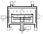
図1に本実施形態に用いられるエピタキシャル成長装置の断面図を示す。図に示すように、例えばφ200mmのSiウェーハwが成膜処理される反応室11には、必要に応じてその内壁を覆うように石英カバー11aが設けられている。 FIG. 1 shows a cross-sectional view of an epitaxial growth apparatus used in this embodiment. As shown in the figure, for example, a
反応室11の上部には、ソースガス、希釈ガスを含むプロセスガスを供給するためのプロセスガス供給機構12と接続されたガス供給口12aが設けられている。そして、反応室11下方には、例えば2か所に、ガスを排出し、反応室11内の圧力を一定(常圧)に制御するためのガス排出機構13と接続されたガス排出口13aが設置されている。 A
ガス供給口12aの下方には、供給されたプロセスガスを整流して供給するための微細貫通孔を有する整流板14が設けられている。 Below the
そして、整流板14の下方には、ウェーハwを載置するための支持部材である、例えばSiCからなるサセプタ15が設けられている。サセプタ15は、回転部材であるリング16上に設置されている。リング16は、ウェーハwを所定の回転速度で回転させる回転軸を介して、モータなどから構成される回転駆動制御機構17と接続されている。 A
リング16内部には、ウェーハwを加熱するための、例えばSiCからなるインヒータ18a、アウトヒータ18bから構成されるヒータが設置されており、それぞれ温度制御機構19と接続されている。そして、これらインヒータ18a、アウトヒータ18bの下部には、ウェーハwを効率的に加熱するための円盤状のリフレクタ20が設置されている。 Inside the
さらに、サセプタ15、インヒータ18a、リフレクタ20を貫通するように、ウェーハwを裏面より支持し、例えば3本のピンを備える突き上げピン21が設置されている。突き上げピン21は、搬入されたウェーハwをサセプタ15の上方で載置し、下降させることにより、ウェーハwをサセプタ15上に載置させることができる。 Further, a push-up pin 21 that supports the wafer w from the back surface and includes, for example, three pins is provided so as to penetrate the
このようなエピタキシャル成長装置を用いて、ウェーハw上に、Siエピタキシャル膜が形成される。 Using such an epitaxial growth apparatus, a Si epitaxial film is formed on the wafer w.
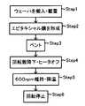
図2にフローチャートを示すように、先ず、搬送アーム(図示せず)などにより、反応室11にウェーハwが搬入される。突き上げピン21上にウェーハwを載置し、下降させることにより、ウェーハwをサセプタ15上に載置する(Step1)。 As shown in the flowchart in FIG. 2, first, the wafer w is loaded into the
次いで、インヒータ18a、アウトヒータ18bを、それぞれ温度制御機構19により所定の温度とすることにより、ウェーハwが例えば1140℃となるように加熱するとともに、回転駆動制御機構17により、ウェーハwを、例えば900rpmで回転させる。 Next, the in-
そして、プロセスガス供給機構12により流量が制御されて混合されたプロセスガスが、整流板14を介して、整流状態でウェーハw上に供給される。プロセスガスは、ソースガスとして例えばトリクロロシランを用い、2.5%となるように希釈ガスであるH2により希釈されて濃度が調整され、例えば50SLMで供給される。Then, process gas flow is mixed is controlled by the process gassupply Organization 12, through the rectifying
一方、余剰となったプロセスガス、反応副生成物であるHClなどからなる排出ガスは、サセプタ15周辺より下方に排出され、ガス排出口13aを介してガス排出機構13により排出される。 On the other hand, surplus process gas, exhaust gas composed of HCl as a reaction by-product, and the like are discharged downward from the periphery of the
このようにして、例えば膜厚が80μmとなるまで、ウェーハw上にSiエピタキシャル膜を成長させる(Step2)。 In this manner, for example, an Si epitaxial film is grown on the wafer w until the film thickness becomes 80 μm (Step 2).
次いで、プロセスガス供給機構12からのソースガスの供給を止め、反応室内のソースガスを排出(ベント)する(Step3)。そして、パージガスとしてH2を供給しながら、回転駆動制御機構17により、例えば20rpm/secで回転数を降下させ、温度制御機構19により、インヒータ18a、アウトヒータ18bの出力を止める(Step4)。Next, the supply of the source gas from the process gas supply mechanism 12 is stopped, and the source gas in the reaction chamber is discharged (vented) (Step 3). Then, while supplying H2 as the purge gas, the rotational
このようにして、回転数を600rpmまで下げ、これを維持したまま、ウェーハwを降温させる(Step5)。そして、ウェーハ温度が800℃程度まで下がった後、回転を停止し、ウェーハを搬出する(Step6)。 In this way, the rotational speed is lowered to 600 rpm, and the temperature of the wafer w is lowered while maintaining this (Step 5). Then, after the wafer temperature falls to about 800 ° C., the rotation is stopped and the wafer is unloaded (Step 6).
このようにしてSiエピタキシャル膜の形成されたウェーハにおいて、スリップの発生状態をXRTにて評価したところ、最大スリップ長:5mm以下、累積スリップ長:20mm以下となった。従来の方法で形成されたウェーハにおける最大スリップ長:50mm、累積スリップ長:650mmと比較して、大きく改善されていることがわかる。 In the wafer having the Si epitaxial film formed as described above, when the occurrence of slip was evaluated by XRT, the maximum slip length was 5 mm or less and the cumulative slip length was 20 mm or less. It can be seen that the maximum slip length of the wafer formed by the conventional method is 50 mm and the cumulative slip length is 650 mm, which is greatly improved.
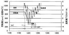
ここで、図3に、ウェーハ温度(In)、回転数、及びオフセット温度(Out−In)の経時変化を示す。成膜時、オフセット温度は最適値である+4℃を維持しているが、ベント時に増大し、回転降下を開始するとともにヒータをオフすると低下し、その後増大する。 Here, FIG. 3 shows changes over time in the wafer temperature (In), the rotation speed, and the offset temperature (Out-In). At the time of film formation, the offset temperature is maintained at the optimum value of + 4 ° C., but increases at the time of venting, starts rotating, decreases and decreases when the heater is turned off, and then increases.
一方、図4に比較例として、回転降下/パージを行い、低速回転とした後、ヒータをオフした従来の工程におけるウェーハ温度(In)、回転数、及びオフセット温度(Out−In)の経時変化を示す。図3に示す本実施形態と比較して、ウェーハ中心部の温度変化は同様であるにもかかわらず、ヒータオフ直後の外周温度の低下が大きくなり、オフセットバランスが大きく崩れていることがわかる。 On the other hand, as a comparative example in FIG. 4, time-dependent changes in wafer temperature (In), rotation speed, and offset temperature (Out-In) in a conventional process in which rotation lowering / purge is performed and low-speed rotation is performed and the heater is turned off. Indicates. Compared to the present embodiment shown in FIG. 3, it can be seen that the temperature change at the center of the wafer is the same, but the decrease in the outer peripheral temperature immediately after the heater is turned off is large, and the offset balance is greatly broken.
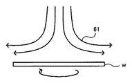
この理由としては、以下のように考えられる。高速回転の場合(例えば600rpm)、図5に模式図を示すように、パージガス51はウェーハwに引き付けられ、ウェーハw上で層流状態となった後、周縁部より排出されるため、温度分布が均一となり、オフセットバランスが保持される。しかしながら、低速回転の場合(例えば100rpm)、図6に模式図を示すように、ウェーハwにパージガス61が引きつけられることなく、周縁部から下方に排出されてしまうため、周縁部の温度が低下(オフセット温度が低下)してしまう。 The reason is considered as follows. In the case of high-speed rotation (for example, 600 rpm), as shown schematically in FIG. 5, the
なお、このようなオフセットバランスを保持することができる回転数は、ウェーハの径、成膜温度などにより変動するが、おおむね、成膜時の回転数の50%以上とすればよい。 Note that the number of rotations that can maintain such an offset balance varies depending on the diameter of the wafer, the film formation temperature, and the like, but it may be about 50% or more of the number of rotations during film formation.
一方、高速回転時には、温度変化によるオフセットバランスへの影響が大きく、ウェーハがズレ易くなる。そこで、オフセットバランスを保持することができる範囲で回転数を下げてから、ヒータをオフすると、オフセットバランスへの影響を抑えることができる。このとき、ヒータをオフしてから実際に温度が低下するまでに、ある程度回転数が下がるため、ヒータオフのタイミングは回転数の降下開始と同時であってもよい。 On the other hand, at the time of high speed rotation, the influence on the offset balance due to the temperature change is large, and the wafer is easily displaced. Therefore, if the heater is turned off after the rotational speed is lowered within a range where the offset balance can be maintained, the influence on the offset balance can be suppressed. At this time, since the rotational speed decreases to some extent after the heater is turned off until the temperature actually decreases, the heater-off timing may be simultaneous with the start of the decrease in the rotational speed.
そして、少なくとも100℃下がるまで(例えば800℃になるまで)、オフセットバランスを保つことができる回転数(例えば600rpm)を維持したまま、降温させることにより、オフセットバランスを崩すことなく、ウェーハを降温させることができる。 Then, the temperature of the wafer is lowered without losing the offset balance by lowering the temperature while maintaining the number of rotations (eg, 600 rpm) that can maintain the offset balance until at least 100 ° C. is lowered (for example, until 800 ° C.). be able to.
本実施形態によれば、オフセットバランスを崩すことなく、ウェーハを降温させることができるため、スリップの発生を抑え、ウェーハにエピタキシャル膜などの膜を高い品質でかつ高い生産性で安定して形成することが可能となる。そして、ウェーハの歩留り向上と共に、素子形成工程及び素子分離工程を経て形成される半導体装置の歩留りの向上、素子特性の安定など信頼性の向上を図ることが可能となる。特にN型ベース領域、P型ベース領域や、絶縁分離領域などに40μm以上の厚膜成長が必要な、パワーMOSFETやIGBTなどのパワー半導体装置のエピタキシャル形成工程に適用されることにより、良好な素子特性を得ることが可能となる。 According to this embodiment, since the temperature of the wafer can be lowered without breaking the offset balance, the occurrence of slip is suppressed, and a film such as an epitaxial film is stably formed on the wafer with high quality and high productivity. It becomes possible. In addition to improving the yield of the wafer, it is possible to improve the reliability of the semiconductor device formed through the element formation process and the element isolation process, such as improvement in yield and stability of element characteristics. In particular, it is a good element by being applied to an epitaxial formation process of a power semiconductor device such as a power MOSFET or IGBT that requires a thick film growth of 40 μm or more in an N-type base region, a P-type base region, an insulating isolation region, or the like. It becomes possible to obtain characteristics.
また、本実施形態においては、Si単結晶層(エピタキシャル膜)形成の場合を説明したが、本実施形態は、ポリSi層、SiC単結晶層形成時にも適用することも可能である。また、例えばSiO2膜やSi3N4膜などSi膜以外の成膜や、例えばGaAs層、GaAlAsやInGaAsなど化合物半導体などにおいても適用することも可能である。その他要旨を逸脱しない範囲で種々変形して実施することができる。In the present embodiment, the case of forming a Si single crystal layer (epitaxial film) has been described. However, the present embodiment can also be applied to the formation of a poly Si layer and a SiC single crystal layer. Further, the present invention can also be applied to film formation other than Si film such as SiO2 film and Si3 N4 film, and compound semiconductor such as GaAs layer, GaAlAs and InGaAs. Various other modifications can be made without departing from the scope of the invention.
11…反応室
11a…石英カバー
12…プロセスガス供給機構
12a…ガス供給口
13…ガス排出機構
13a…ガス排出口
14…整流板
15…サセプタ
16…リング
17…回転駆動制御機構
18a…インヒータ
18b…アウトヒータ
19…温度制御機構
20…リフレクタ
21…突き上げピン
51、61…パージガスDESCRIPTION OF
Claims (5)
Translated fromJapanese前記ウェーハの表面に、ソースガスを含むプロセスガスを供給し、前記ウェーハを所定の第1の回転数で回転させながら、ヒータの出力を制御して前記ウェーハを所定温度に加熱することにより、前記ウェーハの表面に成膜を行い、
成膜後には前記ソースガスの供給を止め、
前記ウェーハの表面にパージガスを供給しながら、前記ウェーハの回転数を、前記第1の回転数から前記ウェーハのオフセットバランスを保持可能な所定の第2の回転数に降下させて維持するとともに、前記ヒータの出力を止め、
前記ウェーハの温度が少なくとも前記所定温度より100℃下がるまで前記第2の回転数で回転させながら前記ウェーハを降温させる、
ことを特徴とする半導体製造方法。Bring the wafer into the reaction chamber, place it on the support member,
By supplying a process gas including a source gas to the surface of the wafer, and rotating the wafer at apredetermined first rotational speed, controlling the output of a heater to heat thewafer to a predetermined temperature, Perform film formation on the wafer surface,
After film formation, the supply of the source gas is stopped,
While supplying a purge gas to the surface of the wafer, the rotational speed of the wafer,the first from the rotational speed is lowered to a second rotational speedof the predetermined capable of holding the offset balance of the waferto maintain Rutotomoni, Stop the heater output,
Lowering the wafer temperature while rotating at the second rotational speeduntil the temperature of the wafer is at least 100 ° C. lower than the predetermined temperature ,
A method of manufacturing a semiconductor.
前記反応室内に設けられ、ウェーハを載置するための支持部材と、A support member provided in the reaction chamber for mounting a wafer;
前記ウェーハの表面に、成膜時にはソースガスを含むプロセスガスを供給し、前記成膜後にはパージガスを供給するプロセス供給機構と、A process supply mechanism for supplying a process gas including a source gas at the time of film formation to the surface of the wafer, and supplying a purge gas after the film formation;
ガスを排出し、反応室内の圧力を制御し、前記成膜後に前記ソースガスをベントするためのガス排出機構と、A gas discharge mechanism for discharging the gas, controlling the pressure in the reaction chamber, and venting the source gas after the film formation;
前記ウェーハの回転数を、成膜時には所定の第1の回転数に維持し、前記成膜後には前記第1の回転数から所定の第2の回転数に降下させ、前記ウェーハの温度が少なくとも前記所定温度より100℃下がるまで維持するように制御する回転駆動制御機構と、The rotation speed of the wafer is maintained at a predetermined first rotation speed during film formation, and after the film formation, the rotation speed is lowered from the first rotation speed to a predetermined second rotation speed, so that the temperature of the wafer is at least A rotation drive control mechanism that controls to maintain the temperature until it falls 100 ° C. below the predetermined temperature;
前記ウェーハを所定温度に加熱するためのヒータと、A heater for heating the wafer to a predetermined temperature;
前記成膜時に、前記ヒータの出力を所定温度となるように制御し、前記成膜が終了し、前記ウェーハの回転数を前記第1の回転数から前記第2の回転数に降下させる際に、前記ヒータの出力を止める温度制御機構と、At the time of film formation, when the output of the heater is controlled to be a predetermined temperature, the film formation is completed, and the rotation speed of the wafer is decreased from the first rotation speed to the second rotation speed. A temperature control mechanism for stopping the output of the heater;
を備えることを特徴とする半導体製造装置。A semiconductor manufacturing apparatus comprising:
Priority Applications (3)
| Application Number | Priority Date | Filing Date | Title |
|---|---|---|---|
| JP2010194323AJP5615102B2 (en) | 2010-08-31 | 2010-08-31 | Semiconductor manufacturing method and semiconductor manufacturing apparatus |
| KR1020110049086AKR101237091B1 (en) | 2010-08-31 | 2011-05-24 | Semiconductor manufacturing method |
| US13/221,565US8951353B2 (en) | 2010-08-31 | 2011-08-30 | Manufacturing method and apparatus for semiconductor device |
Applications Claiming Priority (1)
| Application Number | Priority Date | Filing Date | Title |
|---|---|---|---|
| JP2010194323AJP5615102B2 (en) | 2010-08-31 | 2010-08-31 | Semiconductor manufacturing method and semiconductor manufacturing apparatus |
Publications (2)
| Publication Number | Publication Date |
|---|---|
| JP2012054327A JP2012054327A (en) | 2012-03-15 |
| JP5615102B2true JP5615102B2 (en) | 2014-10-29 |
Family
ID=45697818
Family Applications (1)
| Application Number | Title | Priority Date | Filing Date |
|---|---|---|---|
| JP2010194323AExpired - Fee RelatedJP5615102B2 (en) | 2010-08-31 | 2010-08-31 | Semiconductor manufacturing method and semiconductor manufacturing apparatus |
Country Status (3)
| Country | Link |
|---|---|
| US (1) | US8951353B2 (en) |
| JP (1) | JP5615102B2 (en) |
| KR (1) | KR101237091B1 (en) |
Families Citing this family (5)
| Publication number | Priority date | Publication date | Assignee | Title |
|---|---|---|---|---|
| JP5615102B2 (en)* | 2010-08-31 | 2014-10-29 | 株式会社ニューフレアテクノロジー | Semiconductor manufacturing method and semiconductor manufacturing apparatus |
| CN104681402B (en)* | 2015-03-16 | 2018-03-16 | 京东方科技集团股份有限公司 | Substrate heating equipment and substrate heating method |
| CN106653664B (en)* | 2016-12-07 | 2019-11-15 | 南方科技大学 | GaAs Wafer Deoxygenation Tray |
| WO2019044440A1 (en)* | 2017-09-01 | 2019-03-07 | 株式会社ニューフレアテクノロジー | Vapor-phase growth device and vapor-phase growth method |
| SE543143C2 (en)* | 2019-04-12 | 2020-10-13 | Epiluvac Ab | Device and method for ensuring flatness of wafer during growth |
Family Cites Families (36)
| Publication number | Priority date | Publication date | Assignee | Title |
|---|---|---|---|---|
| US3962716A (en)* | 1973-11-12 | 1976-06-08 | Bell Telephone Laboratories, Incorporated | Reduction of dislocations in multilayer structures of zinc-blend materials |
| US5091333A (en)* | 1983-09-12 | 1992-02-25 | Massachusetts Institute Of Technology | Reducing dislocations in semiconductors utilizing repeated thermal cycling during multistage epitaxial growth |
| US4813732A (en)* | 1985-03-07 | 1989-03-21 | Epsilon Technology, Inc. | Apparatus and method for automated wafer handling |
| US5198034A (en)* | 1987-03-31 | 1993-03-30 | Epsilon Technology, Inc. | Rotatable substrate supporting mechanism with temperature sensing device for use in chemical vapor deposition equipment |
| US4821674A (en)* | 1987-03-31 | 1989-04-18 | Deboer Wiebe B | Rotatable substrate supporting mechanism with temperature sensing device for use in chemical vapor deposition equipment |
| US5080549A (en)* | 1987-05-11 | 1992-01-14 | Epsilon Technology, Inc. | Wafer handling system with Bernoulli pick-up |
| US4836138A (en)* | 1987-06-18 | 1989-06-06 | Epsilon Technology, Inc. | Heating system for reaction chamber of chemical vapor deposition equipment |
| US4975561A (en)* | 1987-06-18 | 1990-12-04 | Epsilon Technology Inc. | Heating system for substrates |
| US5221556A (en)* | 1987-06-24 | 1993-06-22 | Epsilon Technology, Inc. | Gas injectors for reaction chambers in CVD systems |
| US4846102A (en)* | 1987-06-24 | 1989-07-11 | Epsilon Technology, Inc. | Reaction chambers for CVD systems |
| US5261960A (en)* | 1987-06-24 | 1993-11-16 | Epsilon Technology, Inc. | Reaction chambers for CVD systems |
| US5044315A (en)* | 1987-06-24 | 1991-09-03 | Epsilon Technology, Inc. | Apparatus for improving the reactant gas flow in a reaction chamber |
| US5156521A (en)* | 1987-10-15 | 1992-10-20 | Epsilon Technology, Inc. | Method for loading a substrate into a GVD apparatus |
| US5020475A (en)* | 1987-10-15 | 1991-06-04 | Epsilon Technology, Inc. | Substrate handling and transporting apparatus |
| JPH0760804B2 (en)* | 1990-03-20 | 1995-06-28 | 株式会社東芝 | Method and apparatus for semiconductor vapor phase growth |
| JP3725598B2 (en)* | 1996-01-12 | 2005-12-14 | 東芝セラミックス株式会社 | Epitaxial wafer manufacturing method |
| US6126744A (en)* | 1996-11-18 | 2000-10-03 | Asm America, Inc. | Method and system for adjusting semiconductor processing equipment |
| JPH1167675A (en)* | 1997-08-21 | 1999-03-09 | Toshiba Ceramics Co Ltd | High-speed rotating gas-phase thin film forming apparatus and high-speed rotating gas-phase thin film forming method using the same |
| US6252261B1 (en)* | 1998-09-30 | 2001-06-26 | Nec Corporation | GaN crystal film, a group III element nitride semiconductor wafer and a manufacturing process therefor |
| JP4203206B2 (en)* | 2000-03-24 | 2008-12-24 | 株式会社日立国際電気 | Substrate processing equipment |
| DE10024710A1 (en)* | 2000-05-18 | 2001-12-20 | Steag Rtp Systems Gmbh | Setting defect profiles in crystals or crystal-like structures |
| US6783592B2 (en)* | 2002-10-10 | 2004-08-31 | The United States Of America As Represented By The Administrator Of National Aeronautics And Space Administration | Lateral movement of screw dislocations during homoepitaxial growth and devices yielded therefrom free of the detrimental effects of screw dislocations |
| US7682947B2 (en)* | 2003-03-13 | 2010-03-23 | Asm America, Inc. | Epitaxial semiconductor deposition methods and structures |
| US7184657B1 (en)* | 2005-09-17 | 2007-02-27 | Mattson Technology, Inc. | Enhanced rapid thermal processing apparatus and method |
| TWI354320B (en)* | 2006-02-21 | 2011-12-11 | Nuflare Technology Inc | Vopor phase deposition apparatus and support table |
| JP2007251078A (en)* | 2006-03-20 | 2007-09-27 | Nuflare Technology Inc | Vapor growth equipment |
| US20080308036A1 (en) | 2007-06-15 | 2008-12-18 | Hideki Ito | Vapor-phase growth apparatus and vapor-phase growth method |
| JP2009135230A (en)* | 2007-11-29 | 2009-06-18 | Nuflare Technology Inc | Vapor growth film forming apparatus and vapor growth film forming method |
| JP5283370B2 (en)* | 2007-11-29 | 2013-09-04 | 株式会社ニューフレアテクノロジー | Vapor growth apparatus and vapor growth method |
| JP2009135229A (en)* | 2007-11-29 | 2009-06-18 | Nuflare Technology Inc | Vapor growth apparatus and vapor growth method |
| US7967912B2 (en)* | 2007-11-29 | 2011-06-28 | Nuflare Technology, Inc. | Manufacturing apparatus for semiconductor device and manufacturing method for semiconductor device |
| JP2010080909A (en)* | 2008-08-26 | 2010-04-08 | Nuflare Technology Inc | Heater, manufacturing apparatus for semiconductor device, and manufacturing method for semiconductor device |
| TWI397113B (en)* | 2008-08-29 | 2013-05-21 | Veeco Instr Inc | Wafer carrier with varying thermal resistance |
| JP5271648B2 (en)* | 2008-09-22 | 2013-08-21 | 株式会社ニューフレアテクノロジー | Semiconductor manufacturing method and semiconductor manufacturing apparatus |
| JP5615102B2 (en)* | 2010-08-31 | 2014-10-29 | 株式会社ニューフレアテクノロジー | Semiconductor manufacturing method and semiconductor manufacturing apparatus |
| WO2012139006A2 (en)* | 2011-04-07 | 2012-10-11 | Veeco Instruments Inc. | Metal-organic vapor phase epitaxy system and process |
- 2010
- 2010-08-31JPJP2010194323Apatent/JP5615102B2/ennot_activeExpired - Fee Related
- 2011
- 2011-05-24KRKR1020110049086Apatent/KR101237091B1/ennot_activeExpired - Fee Related
- 2011-08-30USUS13/221,565patent/US8951353B2/ennot_activeExpired - Fee Related
Also Published As
| Publication number | Publication date |
|---|---|
| KR101237091B1 (en) | 2013-02-25 |
| KR20120021170A (en) | 2012-03-08 |
| JP2012054327A (en) | 2012-03-15 |
| US8951353B2 (en) | 2015-02-10 |
| US20120052659A1 (en) | 2012-03-01 |
Similar Documents
| Publication | Publication Date | Title |
|---|---|---|
| JP2010129764A (en) | Susceptor, semiconductor manufacturing apparatus, and semiconductor manufacturing method | |
| JP5275935B2 (en) | Semiconductor manufacturing apparatus and semiconductor manufacturing method | |
| JP4956469B2 (en) | Semiconductor manufacturing equipment | |
| JP5615102B2 (en) | Semiconductor manufacturing method and semiconductor manufacturing apparatus | |
| TW201003835A (en) | Susceptor, semiconductor manufacturing apparatus, and semiconductor manufacturing method | |
| TW201135846A (en) | Manufacturing apparatus and method for semiconductor device | |
| US9552983B2 (en) | Manufacturing method for semiconductor device | |
| JP5443096B2 (en) | Semiconductor manufacturing apparatus and semiconductor manufacturing method | |
| KR101422555B1 (en) | Vapor phase growing method and vapor phase growing apparatus | |
| JP5079726B2 (en) | Semiconductor manufacturing method and semiconductor manufacturing apparatus | |
| JP5432608B2 (en) | Semiconductor manufacturing method and semiconductor manufacturing apparatus | |
| JP4933409B2 (en) | Semiconductor manufacturing apparatus and semiconductor manufacturing method | |
| JP5750328B2 (en) | Vapor phase growth method and vapor phase growth apparatus | |
| JP2013051351A (en) | Vapor growth apparatus and vapor growth method | |
| JP5802052B2 (en) | Semiconductor manufacturing apparatus and semiconductor manufacturing method | |
| JP2010074037A (en) | Susceptor, and apparatus and method for manufacturing semiconductor | |
| JP2009135202A (en) | Semiconductor manufacturing apparatus and semiconductor manufacturing method | |
| JP2011198943A (en) | Semiconductor manufacturing apparatus and method thereof | |
| JP2011151118A (en) | Apparatus and method for manufacturing semiconductor | |
| JP5134311B2 (en) | Semiconductor manufacturing apparatus and semiconductor manufacturing method | |
| JP2013048262A (en) | Susceptor, semiconductor manufacturing device, and semiconductor manufacturing method | |
| JP2014116356A (en) | Semiconductor manufacturing method and semiconductor manufacturing device | |
| JP2008066559A (en) | Semiconductor manufacturing method and semiconductor manufacturing apparatus | |
| JP2011066225A (en) | Method of manufacturing semiconductor | |
| JP2011171479A (en) | Semiconductor manufacturing apparatus and semiconductor manufacturing method |
Legal Events
| Date | Code | Title | Description |
|---|---|---|---|
| A621 | Written request for application examination | Free format text:JAPANESE INTERMEDIATE CODE: A621 Effective date:20130403 | |
| A977 | Report on retrieval | Free format text:JAPANESE INTERMEDIATE CODE: A971007 Effective date:20131206 | |
| A131 | Notification of reasons for refusal | Free format text:JAPANESE INTERMEDIATE CODE: A131 Effective date:20140401 | |
| A521 | Request for written amendment filed | Free format text:JAPANESE INTERMEDIATE CODE: A523 Effective date:20140530 | |
| TRDD | Decision of grant or rejection written | ||
| A01 | Written decision to grant a patent or to grant a registration (utility model) | Free format text:JAPANESE INTERMEDIATE CODE: A01 Effective date:20140826 | |
| A61 | First payment of annual fees (during grant procedure) | Free format text:JAPANESE INTERMEDIATE CODE: A61 Effective date:20140909 | |
| R150 | Certificate of patent or registration of utility model | Ref document number:5615102 Country of ref document:JP Free format text:JAPANESE INTERMEDIATE CODE: R150 | |
| R250 | Receipt of annual fees | Free format text:JAPANESE INTERMEDIATE CODE: R250 | |
| R250 | Receipt of annual fees | Free format text:JAPANESE INTERMEDIATE CODE: R250 | |
| R250 | Receipt of annual fees | Free format text:JAPANESE INTERMEDIATE CODE: R250 | |
| R250 | Receipt of annual fees | Free format text:JAPANESE INTERMEDIATE CODE: R250 | |
| R250 | Receipt of annual fees | Free format text:JAPANESE INTERMEDIATE CODE: R250 | |
| R250 | Receipt of annual fees | Free format text:JAPANESE INTERMEDIATE CODE: R250 | |
| LAPS | Cancellation because of no payment of annual fees |