JP5612218B2 - Combination touch, handwriting and fingerprint sensor - Google Patents
Combination touch, handwriting and fingerprint sensorDownload PDFInfo
- Publication number
- JP5612218B2 JP5612218B2JP2013534978AJP2013534978AJP5612218B2JP 5612218 B2JP5612218 B2JP 5612218B2JP 2013534978 AJP2013534978 AJP 2013534978AJP 2013534978 AJP2013534978 AJP 2013534978AJP 5612218 B2JP5612218 B2JP 5612218B2
- Authority
- JP
- Japan
- Prior art keywords
- electrodes
- electrode
- substantially transparent
- implementations
- sensor
- Prior art date
- Legal status (The legal status is an assumption and is not a legal conclusion. Google has not performed a legal analysis and makes no representation as to the accuracy of the status listed.)
- Expired - Fee Related
Links
Images


Classifications
- G—PHYSICS
- G06—COMPUTING OR CALCULATING; COUNTING
- G06F—ELECTRIC DIGITAL DATA PROCESSING
- G06F3/00—Input arrangements for transferring data to be processed into a form capable of being handled by the computer; Output arrangements for transferring data from processing unit to output unit, e.g. interface arrangements
- G06F3/01—Input arrangements or combined input and output arrangements for interaction between user and computer
- G06F3/03—Arrangements for converting the position or the displacement of a member into a coded form
- G06F3/041—Digitisers, e.g. for touch screens or touch pads, characterised by the transducing means
- G06F3/044—Digitisers, e.g. for touch screens or touch pads, characterised by the transducing means by capacitive means
- G—PHYSICS
- G06—COMPUTING OR CALCULATING; COUNTING
- G06F—ELECTRIC DIGITAL DATA PROCESSING
- G06F3/00—Input arrangements for transferring data to be processed into a form capable of being handled by the computer; Output arrangements for transferring data from processing unit to output unit, e.g. interface arrangements
- G06F3/01—Input arrangements or combined input and output arrangements for interaction between user and computer
- G06F3/03—Arrangements for converting the position or the displacement of a member into a coded form
- G06F3/041—Digitisers, e.g. for touch screens or touch pads, characterised by the transducing means
- G—PHYSICS
- G02—OPTICS
- G02B—OPTICAL ELEMENTS, SYSTEMS OR APPARATUS
- G02B26/00—Optical devices or arrangements for the control of light using movable or deformable optical elements
- G02B26/08—Optical devices or arrangements for the control of light using movable or deformable optical elements for controlling the direction of light
- G02B26/0816—Optical devices or arrangements for the control of light using movable or deformable optical elements for controlling the direction of light by means of one or more reflecting elements
- G02B26/0833—Optical devices or arrangements for the control of light using movable or deformable optical elements for controlling the direction of light by means of one or more reflecting elements the reflecting element being a micromechanical device, e.g. a MEMS mirror, DMD
- G—PHYSICS
- G06—COMPUTING OR CALCULATING; COUNTING
- G06F—ELECTRIC DIGITAL DATA PROCESSING
- G06F21/00—Security arrangements for protecting computers, components thereof, programs or data against unauthorised activity
- G06F21/30—Authentication, i.e. establishing the identity or authorisation of security principals
- G06F21/31—User authentication
- G06F21/32—User authentication using biometric data, e.g. fingerprints, iris scans or voiceprints
- G—PHYSICS
- G06—COMPUTING OR CALCULATING; COUNTING
- G06F—ELECTRIC DIGITAL DATA PROCESSING
- G06F21/00—Security arrangements for protecting computers, components thereof, programs or data against unauthorised activity
- G06F21/70—Protecting specific internal or peripheral components, in which the protection of a component leads to protection of the entire computer
- G06F21/82—Protecting input, output or interconnection devices
- G06F21/83—Protecting input, output or interconnection devices input devices, e.g. keyboards, mice or controllers thereof
- G—PHYSICS
- G06—COMPUTING OR CALCULATING; COUNTING
- G06F—ELECTRIC DIGITAL DATA PROCESSING
- G06F3/00—Input arrangements for transferring data to be processed into a form capable of being handled by the computer; Output arrangements for transferring data from processing unit to output unit, e.g. interface arrangements
- G06F3/01—Input arrangements or combined input and output arrangements for interaction between user and computer
- G06F3/03—Arrangements for converting the position or the displacement of a member into a coded form
- G06F3/033—Pointing devices displaced or positioned by the user, e.g. mice, trackballs, pens or joysticks; Accessories therefor
- G06F3/0354—Pointing devices displaced or positioned by the user, e.g. mice, trackballs, pens or joysticks; Accessories therefor with detection of 2D relative movements between the device, or an operating part thereof, and a plane or surface, e.g. 2D mice, trackballs, pens or pucks
- G06F3/03547—Touch pads, in which fingers can move on a surface
- G—PHYSICS
- G06—COMPUTING OR CALCULATING; COUNTING
- G06F—ELECTRIC DIGITAL DATA PROCESSING
- G06F3/00—Input arrangements for transferring data to be processed into a form capable of being handled by the computer; Output arrangements for transferring data from processing unit to output unit, e.g. interface arrangements
- G06F3/01—Input arrangements or combined input and output arrangements for interaction between user and computer
- G06F3/03—Arrangements for converting the position or the displacement of a member into a coded form
- G06F3/041—Digitisers, e.g. for touch screens or touch pads, characterised by the transducing means
- G06F3/0414—Digitisers, e.g. for touch screens or touch pads, characterised by the transducing means using force sensing means to determine a position
- G06F3/04144—Digitisers, e.g. for touch screens or touch pads, characterised by the transducing means using force sensing means to determine a position using an array of force sensing means
- G—PHYSICS
- G06—COMPUTING OR CALCULATING; COUNTING
- G06F—ELECTRIC DIGITAL DATA PROCESSING
- G06F3/00—Input arrangements for transferring data to be processed into a form capable of being handled by the computer; Output arrangements for transferring data from processing unit to output unit, e.g. interface arrangements
- G06F3/01—Input arrangements or combined input and output arrangements for interaction between user and computer
- G06F3/03—Arrangements for converting the position or the displacement of a member into a coded form
- G06F3/041—Digitisers, e.g. for touch screens or touch pads, characterised by the transducing means
- G06F3/0414—Digitisers, e.g. for touch screens or touch pads, characterised by the transducing means using force sensing means to determine a position
- G06F3/04146—Digitisers, e.g. for touch screens or touch pads, characterised by the transducing means using force sensing means to determine a position using pressure sensitive conductive elements delivering a boolean signal and located between crossing sensing lines, e.g. located between X and Y sensing line layers
- G—PHYSICS
- G06—COMPUTING OR CALCULATING; COUNTING
- G06F—ELECTRIC DIGITAL DATA PROCESSING
- G06F3/00—Input arrangements for transferring data to be processed into a form capable of being handled by the computer; Output arrangements for transferring data from processing unit to output unit, e.g. interface arrangements
- G06F3/01—Input arrangements or combined input and output arrangements for interaction between user and computer
- G06F3/03—Arrangements for converting the position or the displacement of a member into a coded form
- G06F3/041—Digitisers, e.g. for touch screens or touch pads, characterised by the transducing means
- G06F3/0416—Control or interface arrangements specially adapted for digitisers
- G06F3/04166—Details of scanning methods, e.g. sampling time, grouping of sub areas or time sharing with display driving
- G—PHYSICS
- G06—COMPUTING OR CALCULATING; COUNTING
- G06F—ELECTRIC DIGITAL DATA PROCESSING
- G06F3/00—Input arrangements for transferring data to be processed into a form capable of being handled by the computer; Output arrangements for transferring data from processing unit to output unit, e.g. interface arrangements
- G06F3/01—Input arrangements or combined input and output arrangements for interaction between user and computer
- G06F3/03—Arrangements for converting the position or the displacement of a member into a coded form
- G06F3/041—Digitisers, e.g. for touch screens or touch pads, characterised by the transducing means
- G06F3/044—Digitisers, e.g. for touch screens or touch pads, characterised by the transducing means by capacitive means
- G06F3/0446—Digitisers, e.g. for touch screens or touch pads, characterised by the transducing means by capacitive means using a grid-like structure of electrodes in at least two directions, e.g. using row and column electrodes
- G—PHYSICS
- G06—COMPUTING OR CALCULATING; COUNTING
- G06F—ELECTRIC DIGITAL DATA PROCESSING
- G06F3/00—Input arrangements for transferring data to be processed into a form capable of being handled by the computer; Output arrangements for transferring data from processing unit to output unit, e.g. interface arrangements
- G06F3/01—Input arrangements or combined input and output arrangements for interaction between user and computer
- G06F3/03—Arrangements for converting the position or the displacement of a member into a coded form
- G06F3/041—Digitisers, e.g. for touch screens or touch pads, characterised by the transducing means
- G06F3/044—Digitisers, e.g. for touch screens or touch pads, characterised by the transducing means by capacitive means
- G06F3/0447—Position sensing using the local deformation of sensor cells
- G—PHYSICS
- G06—COMPUTING OR CALCULATING; COUNTING
- G06F—ELECTRIC DIGITAL DATA PROCESSING
- G06F3/00—Input arrangements for transferring data to be processed into a form capable of being handled by the computer; Output arrangements for transferring data from processing unit to output unit, e.g. interface arrangements
- G06F3/01—Input arrangements or combined input and output arrangements for interaction between user and computer
- G06F3/03—Arrangements for converting the position or the displacement of a member into a coded form
- G06F3/041—Digitisers, e.g. for touch screens or touch pads, characterised by the transducing means
- G06F3/045—Digitisers, e.g. for touch screens or touch pads, characterised by the transducing means using resistive elements, e.g. a single continuous surface or two parallel surfaces put in contact
- G—PHYSICS
- G06—COMPUTING OR CALCULATING; COUNTING
- G06V—IMAGE OR VIDEO RECOGNITION OR UNDERSTANDING
- G06V40/00—Recognition of biometric, human-related or animal-related patterns in image or video data
- G06V40/10—Human or animal bodies, e.g. vehicle occupants or pedestrians; Body parts, e.g. hands
- G06V40/12—Fingerprints or palmprints
- G06V40/13—Sensors therefor
- G06V40/1306—Sensors therefor non-optical, e.g. ultrasonic or capacitive sensing
- G—PHYSICS
- G06—COMPUTING OR CALCULATING; COUNTING
- G06F—ELECTRIC DIGITAL DATA PROCESSING
- G06F2203/00—Indexing scheme relating to G06F3/00 - G06F3/048
- G06F2203/041—Indexing scheme relating to G06F3/041 - G06F3/045
- G06F2203/04103—Manufacturing, i.e. details related to manufacturing processes specially suited for touch sensitive devices
- G—PHYSICS
- G06—COMPUTING OR CALCULATING; COUNTING
- G06F—ELECTRIC DIGITAL DATA PROCESSING
- G06F2203/00—Indexing scheme relating to G06F3/00 - G06F3/048
- G06F2203/041—Indexing scheme relating to G06F3/041 - G06F3/045
- G06F2203/04106—Multi-sensing digitiser, i.e. digitiser using at least two different sensing technologies simultaneously or alternatively, e.g. for detecting pen and finger, for saving power or for improving position detection
- Y—GENERAL TAGGING OF NEW TECHNOLOGICAL DEVELOPMENTS; GENERAL TAGGING OF CROSS-SECTIONAL TECHNOLOGIES SPANNING OVER SEVERAL SECTIONS OF THE IPC; TECHNICAL SUBJECTS COVERED BY FORMER USPC CROSS-REFERENCE ART COLLECTIONS [XRACs] AND DIGESTS
- Y10—TECHNICAL SUBJECTS COVERED BY FORMER USPC
- Y10T—TECHNICAL SUBJECTS COVERED BY FORMER US CLASSIFICATION
- Y10T156/00—Adhesive bonding and miscellaneous chemical manufacture
- Y10T156/10—Methods of surface bonding and/or assembly therefor
- Y—GENERAL TAGGING OF NEW TECHNOLOGICAL DEVELOPMENTS; GENERAL TAGGING OF CROSS-SECTIONAL TECHNOLOGIES SPANNING OVER SEVERAL SECTIONS OF THE IPC; TECHNICAL SUBJECTS COVERED BY FORMER USPC CROSS-REFERENCE ART COLLECTIONS [XRACs] AND DIGESTS
- Y10—TECHNICAL SUBJECTS COVERED BY FORMER USPC
- Y10T—TECHNICAL SUBJECTS COVERED BY FORMER US CLASSIFICATION
- Y10T29/00—Metal working
- Y10T29/49—Method of mechanical manufacture
- Y10T29/49002—Electrical device making
- Y10T29/49117—Conductor or circuit manufacturing
- Y10T29/49124—On flat or curved insulated base, e.g., printed circuit, etc.
Landscapes
- Engineering & Computer Science (AREA)
- Theoretical Computer Science (AREA)
- General Engineering & Computer Science (AREA)
- Physics & Mathematics (AREA)
- General Physics & Mathematics (AREA)
- Human Computer Interaction (AREA)
- Computer Hardware Design (AREA)
- Computer Security & Cryptography (AREA)
- Software Systems (AREA)
- Multimedia (AREA)
- Optics & Photonics (AREA)
- Position Input By Displaying (AREA)
- User Interface Of Digital Computer (AREA)
- Control Of Indicators Other Than Cathode Ray Tubes (AREA)
- Micromachines (AREA)
- Image Input (AREA)
- Mechanical Light Control Or Optical Switches (AREA)
Description
Translated fromJapanese優先権主張
本出願は、参照によりおよびすべての目的のために本明細書に組み込まれる、2010年10月18日に出願され「COMBINATION TOUCH, HANDWRITING AND FINGERPRINT SENSOR」(代理人整理番号第QUALP045P/102908P1号)と題する米国仮特許出願第61/394,054号の優先権を主張する。本出願はまた、参照によりおよびすべての目的のために本明細書に組み込まれる、2011年10月11日に出願され「COMBINATION TOUCH, HANDWRITING AND FINGERPRINT SENSOR」(代理人整理番号第QUALP045A/102908U1号)と題する米国特許出願第13/271,049号の優先権を主張する。PRIORITY CLAIM This application is filed on October 18, 2010 and is incorporated herein by reference and for all purposes as “COMBINATION TOUCH, HANDWRITING AND FINGERPRINT SENSOR”. No.) and claims priority to US Provisional Patent Application No. 61 / 394,054. This application is also filed on October 11, 2011, “COMBINATION TOUCH, HANDWRITING AND FINGERPRINT SENSOR” (Attorney Docket No. QUALP045A / 102908U1), which is incorporated herein by reference and for all purposes. Claims the priority of US patent application Ser. No. 13 / 271,049 entitled
本開示は、限定はしないが、多機能タッチスクリーンを組み込んだディスプレイデバイスを含む、ディスプレイデバイスに関する。 The present disclosure relates to display devices, including but not limited to display devices incorporating a multi-function touch screen.
電気機械システム(EMS:electromechanical system)は、電気的および機械的素子と、アクチュエータと、トランスデューサと、センサと、(ミラーを含む)光学的コンポーネントと、電子回路と、を有するデバイスを含む。電気機械システムは、限定はしないが、マイクロスケールおよびナノスケールを含む、様々なスケールで製造され得る。たとえば、マイクロ電気機械システム(MEMS:microelectromechanical system)デバイスは、約1マイクロメータから数百マイクロメータ以上に及ぶサイズを有する構造を含むことができる。ナノ電気機械システム(NEMS:nanoelectromechanical system)デバイスは、たとえば、数百ナノメートルよりも小さいサイズを含む、1マイクロメータよりも小さいサイズを有する構造を含むことができる。電気および電気機械デバイスを形成するために、堆積、エッチング、リソグラフィを使用して、ならびに/あるいは、基板および/または堆積された材料層の部分をエッチング除去するかまたは層を追加する、他の微細加工プロセスを使用して、電気機械素子が作成され得る。 Electromechanical systems (EMS) include devices having electrical and mechanical elements, actuators, transducers, sensors, optical components (including mirrors), and electronic circuitry. Electromechanical systems can be manufactured on a variety of scales, including but not limited to microscale and nanoscale. For example, a microelectromechanical system (MEMS) device can include a structure having a size ranging from about 1 micrometer to several hundred micrometers or more. Nanoelectromechanical system (NEMS) devices can include structures having a size smaller than 1 micrometer, including, for example, a size smaller than a few hundred nanometers. To form electrical and electromechanical devices, use deposition, etching, lithography and / or other fines to etch away or add portions of the substrate and / or deposited material layers. An electromechanical element can be created using a machining process.
1つのタイプのEMSデバイスは干渉変調器(IMOD:interferometric modulator)と呼ばれる。本明細書で使用する干渉変調器または干渉光変調器という用語は、光学干渉の原理を使用して光を選択的に吸収および/または反射するデバイスを指す。いくつかの実装形態では、干渉変調器は伝導性プレートのペアを含み得、そのペアの一方または両方は、全体的にまたは部分的に、透明でおよび/または反射性であり、適切な電気信号の印加で、相対的に動くことが可能であり得る。一実装形態では、一方のプレートは、基板上に堆積された固定層を含み得、他方のプレートは、エアギャップによって固定層から分離された反射膜を含み得る。別のプレートに対するあるプレートの位置は、干渉変調器に入射する光の光学干渉を変化させることができる。干渉変調器デバイスは、広範囲のアプリケーションを有しており、特にディスプレイ能力がある製品の場合、既存の製品を改善し、新しい製品を作成する際に使用されることが予期される。 One type of EMS device is called an interferometric modulator (IMOD). As used herein, the term interferometric modulator or interferometric light modulator refers to a device that selectively absorbs and / or reflects light using the principles of optical interference. In some implementations, the interferometric modulator may include a pair of conductive plates, one or both of the pairs being wholly or partially transparent and / or reflective, with a suitable electrical signal May be able to move relative to each other. In one implementation, one plate can include a fixed layer deposited on a substrate, and the other plate can include a reflective film separated from the fixed layer by an air gap. The position of one plate relative to another plate can change the optical interference of light incident on the interferometric modulator. Interferometric modulator devices have a wide range of applications and are expected to be used in improving existing products and creating new products, especially for products with display capabilities.
ハンドヘルドデバイスでのタッチスクリーンの使用の増加が、今ではディスプレイ、タッチパネルおよびカバーガラスを含む、モジュールの複雑さおよびコストの増加を引き起こしている。デバイス中の各層は、厚さを追加し、また、隣接する基板への取付けのために、コストがかかるガラス間結合ソリューションを必要とする。これらの問題は、反射型ディスプレイの場合、フロントライトも組み込まれる必要があるとき、モジュールの厚さとコストとを増すので、さらに悪化されることができる。 Increasing use of touch screens in handheld devices has led to increased module complexity and cost, now including displays, touch panels and cover slips. Each layer in the device adds thickness and requires a costly glass-to-glass bonding solution for attachment to an adjacent substrate. These problems can be exacerbated in the case of reflective displays, as it increases the thickness and cost of the module when a front light also needs to be incorporated.
本開示のシステム、方法、およびデバイスは、それぞれいくつかの革新的態様を有し、それらのうちの単一の態様が、単独で、本明細書で開示する望ましい属性を担当するわけではない。本明細書で説明するいくつかの実装形態は、タッチ感知、手書き入力および指紋撮像のための、容量性技術の態様と抵抗性技術の態様とを組み合わせた、複合センサ(combined sensor)デバイスを与える。いくつかのそのような実装形態は、ディスプレイ上にオーバレイされた多特徴(multi-feature)ユーザ入力センサを可能にするために容量性技術と抵抗性技術とを組み合わせたタッチセンサを与える。 Each of the systems, methods, and devices of the present disclosure has several innovative aspects, and no single aspect of them alone is responsible for the desired attributes disclosed herein. Some implementations described herein provide a combined sensor device that combines capacitive and resistive technology aspects for touch sensing, handwriting input and fingerprint imaging. . Some such implementations provide touch sensors that combine capacitive and resistive technologies to allow multi-feature user input sensors overlaid on the display.
いくつかのそのような実装形態では、セルフォン、電子リーダ、またはタブレットコンピュータなど、コンシューマデバイスのカバーガラス装置が、付加的に、シングルタッチまたはマルチタッチセンサ、手書きまたはスタイラス入力デバイス、および/または指紋センサを有する、複合センサデバイスの一部として働く。カバーガラス装置は、2つ、3つまたはそれ以上の層を含み得る。カバーガラス装置を形成するために使用される基板は、実際のガラス、プラスチック、ポリマ、等々のような、様々な好適な実質的に透明な材料から形成され得る。タッチ、手書きおよび/または指紋検出能力を有するそのようなカバーガラス装置は、たとえば、ディスプレイ上にオーバレイされ得る。 In some such implementations, a cover glass device of a consumer device, such as a cell phone, electronic reader, or tablet computer, may additionally include a single touch or multi-touch sensor, a handwriting or stylus input device, and / or a fingerprint sensor As part of a composite sensor device. The cover glass device may include two, three or more layers. The substrate used to form the cover glass device can be formed from a variety of suitable substantially transparent materials, such as actual glass, plastic, polymer, and the like. Such a cover glass device with touch, handwriting and / or fingerprint detection capabilities can be overlaid on a display, for example.
本開示で説明する主題の1つの革新的態様は、第1の実質的に透明な基板を含む装置に実装されることができる。第1の複数の実質的に透明な電極が、第1の実質的に透明な基板の第1の手書きおよびタッチセンサゾーン中に形成され得、第2の複数の実質的に透明な電極が、第1の実質的に透明な基板の第1の指紋センサゾーン中に形成され得る。第1の複数の抵抗器が、第1の複数の電極のうちの、全部ではないが、一部の上に形成され得、第2の複数の抵抗器が、第2の複数の電極上に形成され得る。本装置の手書きセンサゾーンは、第2の複数の電極上に形成された第2の複数の抵抗器を含み得る。 One innovative aspect of the subject matter described in this disclosure can be implemented in an apparatus that includes a first substantially transparent substrate. A first plurality of substantially transparent electrodes may be formed in the first handwriting and touch sensor zone of the first substantially transparent substrate, the second plurality of substantially transparent electrodes being It can be formed in a first fingerprint sensor zone of a first substantially transparent substrate. The first plurality of resistors may be formed on some, but not all, of the first plurality of electrodes, and the second plurality of resistors are on the second plurality of electrodes. Can be formed. The handwriting sensor zone of the apparatus may include a second plurality of resistors formed on the second plurality of electrodes.
本装置は、第2の実質的に透明な基板を含み得る。第3の複数の実質的に透明な電極が、第2の実質的に透明な基板の第2の手書きおよびタッチセンサゾーン中に形成され得る。第4の複数の実質的に透明な電極が、第2の実質的に透明な基板の第2の指紋センサゾーン中に形成され得る。第4の複数の電極は、第2の複数の電極の間隔と実質的に同じである間隔を有し得、第4の複数の電極は、第2の複数の電極の第2の電極位置に対応する第1の電極位置を有し得る。本装置は、第2の複数の電極と第4の複数の電極との間に配設された力感知抵抗器材料を含み得る。 The apparatus can include a second substantially transparent substrate. A third plurality of substantially transparent electrodes may be formed in the second handwriting and touch sensor zone of the second substantially transparent substrate. A fourth plurality of substantially transparent electrodes may be formed in the second fingerprint sensor zone of the second substantially transparent substrate. The fourth plurality of electrodes may have a spacing that is substantially the same as a spacing of the second plurality of electrodes, the fourth plurality of electrodes being at a second electrode position of the second plurality of electrodes. It may have a corresponding first electrode position. The apparatus can include a force sensing resistor material disposed between the second plurality of electrodes and the fourth plurality of electrodes.
第1の複数の抵抗器は、第1の複数の電極の第1のインスタンス上に形成され得る。第1の複数の抵抗器は、第1の複数の電極の第2のインスタンス上には形成されなくても良い。第1の複数の電極の第2のインスタンスは、タッチセンサ電極として構成され得る。タッチセンサ電極は、第3の複数の電極と第1の複数の電極の第2のインスタンスとの間のキャパシタンスの変化を検出するように構成され得る。タッチセンサ電極は、投影容量性タッチセンサ電極として機能するように構成され得る。 The first plurality of resistors may be formed on a first instance of the first plurality of electrodes. The first plurality of resistors may not be formed on the second instance of the first plurality of electrodes. The second instance of the first plurality of electrodes may be configured as a touch sensor electrode. The touch sensor electrode may be configured to detect a change in capacitance between the third plurality of electrodes and the second instance of the first plurality of electrodes. The touch sensor electrode may be configured to function as a projected capacitive touch sensor electrode.
第1の複数の電極の第1のインスタンスは、手書きセンサ電極として構成され得る。第1の複数の電極の第2のインスタンスは、第3の複数の電極と第1の複数の電極の第2のインスタンスとの間の距離の変化によって生じるキャパシタンスの変化を検出するように構成され得る。第1の複数の電極の第2のインスタンスは、加えられた力または圧力によって生じる第2の実質的に透明な基板の変位のアナログ変化を、キャパシタンスの検出された変化に従って判断するように構成され得る。第1の複数の電極の第1のインスタンスは、第3の複数の電極と第1の複数の電極の第1のインスタンスとの間の距離の変化によって生じる抵抗の変化を検出するように構成される。 The first instance of the first plurality of electrodes may be configured as a handwriting sensor electrode. The second instance of the first plurality of electrodes is configured to detect a change in capacitance caused by a change in distance between the third plurality of electrodes and the second instance of the first plurality of electrodes. obtain. The second instance of the first plurality of electrodes is configured to determine an analog change in displacement of the second substantially transparent substrate caused by the applied force or pressure according to the detected change in capacitance. obtain. The first instance of the first plurality of electrodes is configured to detect a change in resistance caused by a change in distance between the third plurality of electrodes and the first instance of the first plurality of electrodes. The
本装置は、第1の複数の電極の第2のインスタンスから第2の基板まで延在する実質的に透明なエラストマ材料をも含み得る。いくつかの実装形態では、実質的に透明なエラストマ材料は、第1の複数の電極の第1のインスタンスから第2の基板まで延在しなくても良い。本装置は、第1の複数の電極と第3の複数の電極との間に配設された実質的に透明な力感知抵抗器材料を含み得る。 The apparatus may also include a substantially transparent elastomeric material that extends from the second instance of the first plurality of electrodes to the second substrate. In some implementations, the substantially transparent elastomeric material may not extend from the first instance of the first plurality of electrodes to the second substrate. The apparatus can include a substantially transparent force sensing resistor material disposed between the first plurality of electrodes and the third plurality of electrodes.
本装置は、ディスプレイと、ディスプレイと通信するように構成されたプロセッサと、を含み得る。プロセッサは、画像データを処理するように構成され得る。本装置は、プロセッサと通信するように構成されたメモリデバイスをも含み得る。本装置は、ディスプレイに少なくとも1つの信号を送るように構成されたドライバ回路と、ドライバ回路に画像データの少なくとも一部分を送るように構成されたコントローラと、をも含み得る。本装置は、プロセッサに画像データを送るように構成された画像ソースモジュールを含み得る。画像ソースモジュールは、受信機、トランシーバ、および送信機のうちの少なくとも1つを含み得る。本装置は、入力データを受信することと、プロセッサに入力データを通信することと、を行うように構成された入力デバイスを含み得る。 The apparatus can include a display and a processor configured to communicate with the display. The processor may be configured to process the image data. The apparatus may also include a memory device configured to communicate with the processor. The apparatus may also include a driver circuit configured to send at least one signal to the display and a controller configured to send at least a portion of the image data to the driver circuit. The apparatus may include an image source module configured to send image data to the processor. The image source module may include at least one of a receiver, a transceiver, and a transmitter. The apparatus can include an input device configured to receive input data and communicate the input data to a processor.
本開示で説明する主題の別の革新的態様は、第1の実質的に透明な基板を含む代替装置に実装されることができる。第1の電極アレイが、第1の実質的に透明な基板の第1の手書きおよびタッチセンサゾーン中に形成され得る。第2の電極アレイが、第1の実質的に透明な基板の第1の指紋センサゾーン中に形成され得る。いくつかの実装形態では、第2の電極アレイは、第1の電極アレイよりも近接して離間され得る。しかしながら、他の実装形態では、第2の電極アレイは、第1の電極アレイよりも近接して離間されなくても良い。 Another innovative aspect of the subject matter described in this disclosure can be implemented in an alternative device that includes a first substantially transparent substrate. A first electrode array may be formed in the first handwriting and touch sensor zone of the first substantially transparent substrate. A second electrode array may be formed in the first fingerprint sensor zone of the first substantially transparent substrate. In some implementations, the second electrode array can be spaced closer than the first electrode array. However, in other implementations, the second electrode array may not be spaced closer than the first electrode array.
第1の抵抗器が、第1の電極アレイのうちの、全部ではないが、一部の上に形成され得る。第2の抵抗器が第2の電極アレイ上に形成され得る。 The first resistor may be formed on some but not all of the first electrode array. A second resistor may be formed on the second electrode array.
本装置は、第2の実質的に透明な基板を含み得る。第3の電極アレイが、第2の実質的に透明な基板の第2の手書きおよびタッチセンサゾーン中に形成され得る。第4の電極アレイが、第2の実質的に透明な基板の第2の指紋センサゾーン中に形成され得る。第4の電極アレイは、第2の電極アレイの間隔と実質的に同じである間隔を有し得る。第4の電極アレイは、第2の電極アレイの第2の電極位置に対応する第1の電極位置を有し得る。 The apparatus can include a second substantially transparent substrate. A third electrode array may be formed in the second handwriting and touch sensor zone of the second substantially transparent substrate. A fourth electrode array may be formed in the second fingerprint sensor zone of the second substantially transparent substrate. The fourth electrode array may have a spacing that is substantially the same as the spacing of the second electrode array. The fourth electrode array may have a first electrode position that corresponds to the second electrode position of the second electrode array.
第1の抵抗器は、第1の電極アレイ中の電極の第1のインスタンス上に形成され得る。第1の抵抗器は、第1の電極アレイ中の電極の第2のインスタンス上には形成されなくても良い。電極の第2のインスタンスはタッチセンサ電極として構成され得る。本装置は、第3の電極アレイの電極と電極の第2のインスタンスとの間のキャパシタンスの変化を検出するように構成され得る。本装置は、投影容量性タッチセンサ動作のために構成され得る。電極の第1のインスタンスは手書きセンサ電極を含み得る。本装置は、第3の電極アレイの電極と電極の第2のインスタンスとの間の距離の変化によって生じるキャパシタンスの変化を検出するように構成され得る。本装置は、第3の電極アレイの電極と電極の第1のインスタンスとの間の距離の変化によって生じる抵抗の変化を検出するように構成され得る。
The first resistor can be formed on a first instance of an electrode in the first electrode array. The first resistor may not be formed on the second instance of the electrode in the first electrode array. The second instance of the electrode may be configured as a touch sensor electrode. The apparatus can be configured to detect a change in capacitance between an electrode of the third electrode array and a second instance of the electrode. The apparatus can be configured for projected capacitive touch sensor operation. The firstinstanceof the electrodesmay include a handwriting sensor electrode. The apparatus can be configured to detect a change in capacitance caused by a change in distance between an electrode of the third electrode array and a second instance of the electrode. The apparatus may be configured to detect a change in resistance caused by a change in distance between the electrodes of the third electrode array and the first instance of the electrodes.
本開示で説明する主題の別の革新的態様は、第1の手書きおよびタッチセンサゾーン中に形成された第1の複数の実質的に透明な電極と、第1の指紋センサゾーン中に形成された第2の複数の実質的に透明な電極と、を有する第1の実質的に透明な基板を含む代替装置において実装され得る。第2の複数の電極は、実装形態に応じて、第1の複数の電極よりも近接して離間されても良いし離間されなくても良い。本装置は、第1の複数の電極のうちの、全部ではないが、一部の上に形成された第1の複数の抵抗器と、第2の複数の電極上に形成された第2の複数の抵抗器と、を含み得る。 Another innovative aspect of the subject matter described in this disclosure is a first plurality of substantially transparent electrodes formed in the first handwriting and touch sensor zone and formed in the first fingerprint sensor zone. And may be implemented in an alternative device that includes a first substantially transparent substrate having a second plurality of substantially transparent electrodes. The second plurality of electrodes may or may not be spaced closer to each other than the first plurality of electrodes, depending on the mounting form. The device includes a first plurality of resistors formed on a part, if not all, of the first plurality of electrodes and a second plurality of electrodes formed on the second plurality of electrodes. A plurality of resistors.
本装置は、第2の手書きおよびタッチセンサゾーン中に形成された第3の複数の実質的に透明な電極と、第2の指紋センサゾーン中に形成された第4の複数の実質的に透明な電極と、を有する第2の実質的に透明な基板を含み得る。第4の複数の電極は、第2の複数の電極の間隔と実質的に同じである間隔を有し得る。第4の複数の電極は、第2の複数の電極の電極位置に対応する電極位置を有し得る。 The apparatus includes a third plurality of substantially transparent electrodes formed in the second handwriting and touch sensor zone and a fourth plurality of substantially transparent electrodes formed in the second fingerprint sensor zone. And a second substantially transparent substrate having a transparent electrode. The fourth plurality of electrodes may have a spacing that is substantially the same as a spacing of the second plurality of electrodes. The fourth plurality of electrodes may have electrode positions corresponding to the electrode positions of the second plurality of electrodes.
本装置は、第2および第4の複数の実質的に透明な電極との通信のために構成されたセンサ制御システムを含み得る。センサ制御システムは、第2および第4の複数の実質的に透明な電極から受信した電気信号に従って指紋センサデータを処理するようにさらに構成され得る。 The apparatus can include a sensor control system configured for communication with the second and fourth plurality of substantially transparent electrodes. The sensor control system may be further configured to process the fingerprint sensor data in accordance with electrical signals received from the second and fourth plurality of substantially transparent electrodes.
センサ制御システムは、第1および第3の複数の実質的に透明な電極との通信のためにさらに構成され得る。センサ制御システムは、第1および第3の複数の実質的に透明な電極から受信した電気信号に従って手書きおよびタッチセンサデータを処理するようにさらに構成され得る。 The sensor control system may be further configured for communication with the first and third plurality of substantially transparent electrodes. The sensor control system may be further configured to process handwriting and touch sensor data in accordance with electrical signals received from the first and third plurality of substantially transparent electrodes.
本装置は、ディスプレイと、ディスプレイと通信するように構成されたプロセッサと、を含み得る。プロセッサは、画像データを処理するように構成され得る。本装置は、プロセッサと通信するように構成されたメモリデバイスを含み得る。いくつかの実装形態では、センサ制御システムは、プロセッサを含む。別の実装形態では、センサ制御システムは、プロセッサとは別個であるが、プロセッサとの通信のために構成される。プロセッサは、少なくとも部分的に、センサ制御システムから受信した信号に従って、ディスプレイを制御するように構成され得る。プロセッサは、少なくとも部分的に、センサ制御システムから受信した信号に従って、ディスプレイへのアクセスを制御するように構成され得る。プロセッサは、少なくとも部分的に、センサ制御システムから受信したユーザ入力信号に従って、ディスプレイを制御するように構成され得る。 The apparatus can include a display and a processor configured to communicate with the display. The processor may be configured to process the image data. The apparatus can include a memory device configured to communicate with a processor. In some implementations, the sensor control system includes a processor. In another implementation, the sensor control system is separate from the processor but is configured for communication with the processor. The processor may be configured to control the display at least in part according to signals received from the sensor control system. The processor may be configured to control access to the display at least in part according to signals received from the sensor control system. The processor may be configured to control the display at least in part according to user input signals received from the sensor control system.
本明細書で説明する主題の1つまたは複数の実装形態の詳細が、添付の図面および以下の説明において示されている。本概要で与えた例は、主にMEMSベースのディスプレイに関して説明されているが、本明細書で提供する概念は、液晶ディスプレイ、有機発光ダイオード(「OLED」)ディスプレイおよび電界放出ディスプレイなど、他のタイプのディスプレイに適用され得る。他の特徴、態様、および利点は、説明、図面、および特許請求の範囲から明らかになるであろう。以下の図の相対寸法は一定の縮尺で描かれていないことがあることに留意されたい。 The details of one or more implementations of the subject matter described in this specification are set forth in the accompanying drawings and the description below. While the examples given in this summary have been described primarily with respect to MEMS-based displays, the concepts provided herein are not limited to other liquid crystal displays, organic light emitting diode (“OLED”) displays, and field emission displays. Can be applied to types of displays. Other features, aspects, and advantages will be apparent from the description, drawings, and claims. Note that the relative dimensions in the following figures may not be drawn to scale.
様々な図面中の同様の参照番号および名称は、同様の要素を示す。 Like reference numbers and designations in the various drawings indicate like elements.
以下の説明は、本開示の革新的態様について説明する目的で、いくつかの実装形態を対象とする。ただし、本明細書の教示が多数の異なる方法で適用され得ることを、当業者は容易に認識されよう。説明する実装形態は、動いていようと(たとえば、ビデオ)、静止していようと(たとえば、静止画像)、およびテキストであろうと、グラフィックであろうと、絵であろうと、画像を表示するように構成され得る任意のデバイスまたはシステムにおいて実装され得る。より詳細には、説明する実装形態は、限定はしないが、携帯電話、マルチメディアインターネット対応セルラ電話、モバイルテレビジョン受信機、ワイヤレスデバイス、スマートフォン、Bluetooth(登録商標)デバイス、携帯情報端末(PDA)、ワイヤレス電子メール受信機、ハンドヘルドまたはポータブルコンピュータ、ネットブック、ノートブック、スマートブック、タブレット、プリンタ、コピー機、スキャナ、ファクシミリデバイス、GPS受信機/ナビゲータ、カメラ、MP3プレーヤ、カムコーダ、ゲーム機、腕時計、クロック、計算器、テレビジョンモニタ、フラットパネルディスプレイ、電子リーディングデバイス(すなわち、電子リーダ)、コンピュータモニタ、自動車ディスプレイ(オドメータおよびスピードメータディスプレイなどを含む)、コックピットコントロールおよび/またはディスプレイ、カメラビューディスプレイ(車両における後部ビューカメラのディスプレイなど)、電子写真、電子ビルボードまたは標示、プロジェクタ、アーキテクチャ構造物、電子レンジ、冷蔵庫、ステレオシステム、カセットレコーダーまたはプレーヤ、DVDプレーヤ、CDプレーヤ、VCR、ラジオ、ポータブルメモリチップ、洗濯機、乾燥機、洗濯機/乾燥機、パーキングメータ、(電気機械システム、マイクロ電気機械システム、および非MEMS適用例などにおける)パッケージング、審美構造物(たとえば、1つの宝飾品上の画像のディスプレイ)、ならびに様々なEMSデバイスなど、様々な電子デバイス中に含まれるかまたはそれらに関連付けられ得ると考えられる。また、本明細書の教示は、限定はしないが、電子スイッチングデバイス、無線周波フィルタ、センサ、加速度計、ジャイロスコープ、動き感知デバイス、磁力計、コンシューマエレクトロニクスのための慣性コンポーネント、コンシューマエレクトロニクス製品の部品、バラクタ、液晶デバイス、電気泳動デバイス、駆動方式、製造プロセスおよび電子テスト機器など、非ディスプレイ適用例において使用され得る。したがって、本教示は、単に図に示す実装形態に限定されるものではなく、代わりに、当業者に直ちに明らかになるであろう広い適用性を有する。 The following description is directed to several implementations for purposes of describing the innovative aspects of the disclosure. However, one of ordinary skill in the art will readily recognize that the teachings herein can be applied in a number of different ways. The described implementation is to display an image, whether it is moving (eg, video), static (eg, still image), and text, graphic, picture, picture It can be implemented in any device or system that can be configured. More specifically, the described implementations include, but are not limited to, cellular phones, multimedia internet-enabled cellular phones, mobile television receivers, wireless devices, smartphones, Bluetooth® devices, personal digital assistants (PDAs) , Wireless email receivers, handheld or portable computers, netbooks, notebooks, smart books, tablets, printers, copiers, scanners, facsimile devices, GPS receivers / navigators, cameras, MP3 players, camcorders, game consoles, watches Clocks, calculators, television monitors, flat panel displays, electronic reading devices (ie electronic readers), computer monitors, automotive displays (odometers and Including a meter display), cockpit control and / or display, camera view display (such as a rear view camera display in a vehicle), electrophotography, electronic billboard or sign, projector, architectural structure, microwave oven, refrigerator, stereo System, cassette recorder or player, DVD player, CD player, VCR, radio, portable memory chip, washing machine, dryer, washing machine / dryer, parking meter, (electromechanical system, microelectromechanical system, and non-MEMS applications Included in or on various electronic devices, such as packaging (in examples), aesthetic structures (eg, display of images on one jewelery), and various EMS devices. It is considered to be affixed with each other. The teachings herein also include, but are not limited to, electronic switching devices, radio frequency filters, sensors, accelerometers, gyroscopes, motion sensing devices, magnetometers, inertial components for consumer electronics, parts of consumer electronics products It can be used in non-display applications such as varactors, liquid crystal devices, electrophoretic devices, drive systems, manufacturing processes and electronic test equipment. Accordingly, the present teachings are not limited to the implementations shown solely in the Figures, but instead have broad applicability that will be readily apparent to those skilled in the art.
本明細書で説明するいくつかの実装形態は、タッチ感知、手書き入力のためのスタイラス検出、および指紋撮像のための、容量性技術の新規の態様と抵抗性技術の新規の態様とを組み合わせる。いくつかのそのような実装形態は、その少なくとも一部が、ディスプレイ上にオーバレイされるかまたはさもなければディスプレイと組み合わされ得る、カバーガラス装置に組み込まれる、複合センサデバイスを与える。カバーガラス装置は、2つ、3つまたはそれ以上の層を有し得る。いくつかの実装形態では、カバーガラス装置は、実質的に透明でフレキシブルな上側基板と、実質的に透明で比較的より堅い下側基板と、を含む。いくつかのそのような実装形態では、カバーガラス装置の下側基板は、ディスプレイ基板上にオーバレイされ得る。別の実装形態では、カバーガラス装置の下側基板は、ディスプレイ基板であり得る。たとえば、カバーガラス装置の下側基板は、以下で説明するように、IMODデバイスがその上に作製されたのと同じ透明基板であり得る。 Some implementations described herein combine a novel aspect of capacitive technology and a novel aspect of resistive technology for touch sensing, stylus detection for handwriting input, and fingerprint imaging. Some such implementations provide a composite sensor device that is incorporated into a cover glass apparatus, at least a portion of which can be overlaid on the display or otherwise combined with the display. Cover glass devices can have two, three or more layers. In some implementations, the cover glass device includes a substantially transparent and flexible upper substrate and a substantially transparent and relatively stiffer lower substrate. In some such implementations, the lower substrate of the cover glass device can be overlaid on the display substrate. In another implementation, the lower substrate of the cover glass device can be a display substrate. For example, the lower substrate of the cover glass device can be the same transparent substrate on which the IMOD device was fabricated, as described below.
そのようなセンサデバイスの様々な実装形態が本明細書で説明される。いくつかの実装形態では、ディスプレイデバイスのカバーガラスは、シングルタッチまたはマルチタッチセンサとして、手書き(またはメモキャプチャ)入力デバイスとして、および指紋センサとして、働く。センサの機能および分解能は、カバーガラス上の特定のロケーションに合わせて調整され得る。いくつかのそのような実装形態では、指紋感知素子が配置されたエリアが、指紋検出だけでなく、手書きおよびタッチ機能をも提供し得る。いくつかの他の実装形態では、指紋センサは、指紋機能のみを提供する別個の高分解能ゾーンに分離され得る。いくつかの実装形態では、センサデバイスは、組合せタッチおよびスタイラス入力デバイスとして働く。様々な作製方法が、複合センサデバイスを含むデバイスを使用するための方法に加えて、本明細書で説明される。 Various implementations of such sensor devices are described herein. In some implementations, the cover glass of the display device serves as a single touch or multi-touch sensor, as a handwriting (or memo capture) input device, and as a fingerprint sensor. The function and resolution of the sensor can be adjusted for a specific location on the cover glass. In some such implementations, the area in which the fingerprint sensing element is located can provide not only fingerprint detection, but also handwriting and touch functionality. In some other implementations, the fingerprint sensor may be separated into separate high resolution zones that provide only the fingerprint function. In some implementations, the sensor device acts as a combined touch and stylus input device. Various fabrication methods are described herein in addition to methods for using devices including composite sensor devices.
本開示で説明する主題の特定の実装形態は、以下の潜在的な利点のうちの1つまたは複数を実現するように実装されることができる。本明細書で説明するいくつかの実装形態は、タッチ感知、手書き入力、および場合によっては指紋撮像のための、容量性技術の態様と抵抗性技術の態様とを組み合わせる。いくつかのそのような実装形態は、ディスプレイ上にオーバレイされることができる多機能ユーザ入力センサを可能にするために、容量性技術と抵抗性技術とを組み合わせたタッチセンサを与える。複合センサデバイスのいくつかの実装形態は、何らかの従来の投影容量性タッチ(PCT:projected capacitive touch)ベースのデバイスにおける、カバーガラスとディスプレイガラスとの間に配設される中間タッチセンサ層を無くす。したがって、いくつかのそのような実装形態は、PCT技術および抵抗性技術の少なくともいくつかの欠点を緩和するかまたは無くすことができる。 Particular implementations of the subject matter described in this disclosure can be implemented to realize one or more of the following potential advantages. Some implementations described herein combine aspects of capacitive technology and aspects of resistive technology for touch sensing, handwriting input, and possibly fingerprint imaging. Some such implementations provide a touch sensor that combines capacitive and resistive technology to allow a multifunction user input sensor that can be overlaid on the display. Some implementations of composite sensor devices eliminate the intermediate touch sensor layer disposed between the cover glass and the display glass in any conventional projected capacitive touch (PCT) based device. Thus, some such implementations can mitigate or eliminate at least some of the disadvantages of PCT technology and resistive technology.
ハイブリッドPCTおよびデジタル抵抗タッチ(DRT:digital resistive touch)実装形態は、たとえば、DRT態様を用いて、ディスプレイ上への細いスタイラス先端の押圧の検出を可能にしながら、PCT態様を使用して、指によるディスプレイ上での極めて軽いブラッシングまたは近接したホバリングの検出をも可能にする。センサデバイスは、通電しているか通電していないかにかかわらず、任意の形態のスタイラスまたはペン入力を受け付けることができる。透明なまたは事実上透明な力感知抵抗器が、光学的および電気的性能を改善するために、センセルの一部または全部の内部に含まれ得る。 Hybrid PCT and digital resistive touch (DRT) implementations use, for example, a finger by using the PCT aspect while allowing detection of a thin stylus tip press on the display using the DRT aspect. It also enables detection of very light brushing or close hovering on the display. The sensor device can accept any form of stylus or pen input, whether energized or not energized. Transparent or virtually transparent force-sensing resistors can be included within some or all of the sensing cells to improve optical and electrical performance.
いくつかの実装形態によれば、複合センサ(combination sensor)は、それらのうちのいくつかは異なる基板上にあり得る、2つ以上のパターニングされた層を含み得る。上側(または外側)基板は、たとえば、ポリエチレンテレフタラート(PET)、ポリエチレンナフタレート(PEN)、ポリイミド、または同様の材料など、プラスチックから形成され得る。上側基板はまた、実質的に透明であり得、また、それの下面(underside)にパターニングされた酸化インジウムスズ(ITO)などの実質的に透明な導体を有し得る。下側基板は、別の好適な材料とともに、ガラスなどの実質的に透明な基板材料から形成され得る。実質的に透明な基板の上表面(top surface)は、ITOなどの実質的に透明な導体材料のパターニングされた層であるこができる。いくつかの実装形態では、上側基板の下面上の導体と、下側基板の上側面(upper side)上の導体とは、ダイヤモンド形電極にパターニングされ、2つの異なる層の各々の上の行または列として接続され得る。 According to some implementations, a combination sensor can include two or more patterned layers, some of which can be on different substrates. The upper (or outer) substrate may be formed from a plastic such as, for example, polyethylene terephthalate (PET), polyethylene naphthalate (PEN), polyimide, or similar material. The upper substrate can also be substantially transparent and can have a substantially transparent conductor, such as indium tin oxide (ITO) patterned on its underside. The lower substrate can be formed from a substantially transparent substrate material, such as glass, with another suitable material. The top surface of the substantially transparent substrate can be a patterned layer of a substantially transparent conductive material such as ITO. In some implementations, the conductors on the lower surface of the upper substrate and the conductors on the upper side of the lower substrate are patterned into diamond-shaped electrodes and are either in rows above each of the two different layers or Can be connected as a row.
いくつかのそのような実装形態は、センサデバイスのフレキシブル上側基板が、信号線、電気接地、および電力のルーティングを可能にするために、延長部分上のパターニングされた金属被覆を有する、ラップアラウンド構成を含む。このフレキシブル上側基板は、カバーガラス装置の比較的より堅い下側基板のエッジの周りに巻かれ得る。接続ソケットを含む、1つまたは複数のICまたは受動コンポーネントが、コストおよび複雑さを低減するために、フレキシブル層上に取り付けられ得る。下側基板上のセンサ電極をアドレス指定する信号線が、フレキシブル上側基板の下面上の対応するパターンにルーティングされ、接続され得る。そのような実装形態は、集積回路および/または他のデバイスに上側層の信号線を電気的に接続するためのフレックスケーブルの必要性を無くすという潜在的な利点を有する。その手法は、最終的なカバーガラス装置のいくつかのバージョンのためのベゼルレス構成を可能にする。 Some such implementations include a wrap-around configuration where the flexible upper substrate of the sensor device has a patterned metallization on the extension to allow routing of signal lines, electrical ground, and power. including. This flexible upper substrate can be wrapped around the edge of the relatively stiffer lower substrate of the cover glass device. One or more ICs or passive components, including connection sockets, can be mounted on the flexible layer to reduce cost and complexity. Signal lines that address sensor electrodes on the lower substrate can be routed and connected to corresponding patterns on the lower surface of the flexible upper substrate. Such an implementation has the potential advantage of eliminating the need for flex cables to electrically connect upper layer signal lines to integrated circuits and / or other devices. That approach allows for a bezelless configuration for several versions of the final cover glass device.
作製方法は、下にあるディスプレイの光学的性能を増加させるために、主として透明な基板および材料を含む。作製プロセスは、センサデバイスの少なくとも一部分のためにフレキシブル基板を利用し、低コストのためのロールツーロール処理に役立ち得る。 The fabrication method involves primarily transparent substrates and materials to increase the optical performance of the underlying display. The fabrication process utilizes a flexible substrate for at least a portion of the sensor device and can aid in roll-to-roll processing for low cost.
組合せセンサの上側部分と下側部分との間の近ブライアンとエラストマ層の使用は、スタイラスからの加えられた圧力または力に対する感度を増加させながら、所与のセンセルピッチについて横方向分解能を増加させることができる。エラストマ材料は、力感知抵抗器の包含のためのオープン領域を含み得る。エラストマ材料およびFSR材料の慎重な選択により、エアギャップに伴うことができる透過率の損失が、最小限に抑えられる。 The use of a near Brian and elastomer layer between the upper and lower portions of the combined sensor increases lateral resolution for a given sensell pitch while increasing sensitivity to applied pressure or force from the stylus. Can do. The elastomeric material may include an open area for the inclusion of force sensing resistors. Careful selection of elastomeric and FSR materials minimizes the transmission loss that can accompany the air gap.
力感知スイッチとローカルキャパシタとのアレイが、ローカルキャパシタを関連するPCT検出回路に接続するために使用され得るもので、その場合、各キャパシタは、力感知スイッチがスタイラスまたは指の押圧によって閉じられたとき、高いキャパシタンス増加を達成するように、薄い誘電体層で形成される。したがって、同じPCT検出回路が、指でタッチされたとき(タッチモード)の相互キャパシタンスの変化と、力感知スイッチが押下されたとき(スタイラスまたは指紋モード)のセンセルキャパシタンスの変化と、を検出するために、使用されることができる。 An array of force sensitive switches and local capacitors can be used to connect the local capacitors to the associated PCT detection circuit, where each capacitor is closed by a stylus or finger press. Sometimes formed with a thin dielectric layer to achieve a high capacitance increase. Thus, the same PCT detection circuit detects the change in mutual capacitance when touched with a finger (touch mode) and the change in sensor cell capacitance when the force sensing switch is pressed (stylus or fingerprint mode). Can be used for.
組合せ多機能センサデバイスは、単一のタッチスクリーンが手書き入力および指紋認識などの追加機能を実行することをできるようにする。いくつかの実装形態では、これらの複数の特徴は、ユーザ認証を介するセキュリティの増強を可能にし、手書きのより良いキャプチャと、ユーザインターフェースへのより対話型の手法と、を可能にする。センサデバイスを有するセルフォンなどのハンドヘルドモバイルデバイスは、トランザクションおよび物理的アクセスを可能にするためのユーザ認証のためのゲートウェイとしてモバイルデバイスを使用すること、トランザクションアプリケーションのための署名認識および送信のために手書き入力機能を使用すること、ならびに、学問の環境では生徒の、または企業の環境では従業員の、メモおよび他のドキュメントを自動的にキャプチャするために手書き入力特徴を使用すること、を含む、アプリケーションのアレイを可能にする。 The combined multifunction sensor device allows a single touch screen to perform additional functions such as handwriting input and fingerprint recognition. In some implementations, these multiple features allow for increased security through user authentication, allowing better capture of handwriting and a more interactive approach to the user interface. Handheld mobile devices such as cell phones with sensor devices use the mobile device as a gateway for user authentication to enable transactions and physical access, handwriting for signature recognition and transmission for transaction applications Applications that include using input features and using handwritten input features to automatically capture notes and other documents of students in an academic environment or of employees in a corporate environment Allows an array of
いくつかのそのような実装形態では、別個のコントローラがセンサデバイスのために構成され得、または、そのコントローラはアプリケーションプロセッサの一部として含まれ得る。手書き、タッチおよび指紋検出のためのソフトウェアが、1つまたは複数のコントローラまたはアプリケーションプロセッサ上に含まれ得る。低い分解能、中間の分解能および高い分解能は、センセルのサブセットを走査することによって、あるいは線または列をアグリゲートすることによって、単一のセンサデバイスを用いて取得されることができる。電力消費は、より大きいアレイとともにより高い分解能が必要とされるまで、センサピクセル(または行または列)が低電力小アレイとして機能するように、コントローラを使用してそれらのセンサピクセルを電気的にアグリゲートすることによって、低減され得る。電力消費は、センサデバイスの部分または全部をオフにするか、コントローラの一部をオフにするか、または低減されたフレームレートで第1レベルスクリーニングを採用することによって、低減され得る。いくつかのそのような実装形態では、組合せPCTセンサおよびデジタル抵抗タッチ(DRT)センサは、キャパシタのパッシブアレイ(PCT)と抵抗スイッチのパッシブアレイ(DRT)とを有する。タッチセンサシステムとスタイラスセンサシステムは、概して、異なる感知技法を使用するが、共通の構造を用いたホリスティック手法は、PCB部品数を節約し、ASIC実装形態におけるエリアを低減し、電力を低減し、タッチサブシステムとスタイラスサブシステムとの間の隔離の必要を無くす。 In some such implementations, a separate controller may be configured for the sensor device, or the controller may be included as part of the application processor. Software for handwriting, touch and fingerprint detection may be included on one or more controllers or application processors. Low resolution, medium resolution and high resolution can be obtained with a single sensor device by scanning a subset of the sensors or by aggregating lines or columns. Power consumption is achieved by using a controller to electrically connect the sensor pixels (or rows or columns) so that the sensor pixels (or rows or columns) function as a low power small array until higher resolution is required with larger arrays. It can be reduced by aggregating. Power consumption can be reduced by turning off part or all of the sensor device, turning off part of the controller, or employing first level screening with a reduced frame rate. In some such implementations, the combined PCT sensor and digital resistive touch (DRT) sensor have a passive array of capacitors (PCT) and a passive array of resistive switches (DRT). Touch sensor systems and stylus sensor systems generally use different sensing techniques, but a holistic approach with a common structure saves PCB component count, reduces area in ASIC implementation, and reduces power. Eliminates the need for isolation between the touch subsystem and the stylus subsystem.
説明する実装形態が適用され得る好適なEMSまたはMEMSデバイスの一例は反射型ディスプレイデバイスである。反射型ディスプレイデバイスは、光学干渉の原理を使用してそれに入射する光を選択的に吸収および/または反射するために干渉変調器(IMOD)を組み込むことができる。IMODは、吸収体、吸収体に対して可動である反射体、ならびに吸収体と反射体との間に画定された光共振キャビティを含むことができる。反射体は、2つ以上の異なる位置に移動され得、これは、光共振キャビティのサイズを変化させ、それにより干渉変調器の反射率に影響を及ぼすことがある。IMODの反射スペクトルは、かなり広いスペクトルバンドをもたらすことができ、そのスペクトルバンドは、異なる色を生成するために可視波長にわたってシフトされ得る。スペクトルバンドの位置は、光共振キャビティの厚さを変更することによって調整され得る。光共振キャビティを変更する1つの方法は、反射体の位置を変更することによる方法である。 An example of a suitable EMS or MEMS device to which the described implementation can be applied is a reflective display device. A reflective display device can incorporate an interferometric modulator (IMOD) to selectively absorb and / or reflect light incident thereon using the principle of optical interference. The IMOD can include an absorber, a reflector that is movable relative to the absorber, and an optical resonant cavity defined between the absorber and the reflector. The reflector can be moved to two or more different positions, which can change the size of the optical resonant cavity, thereby affecting the reflectivity of the interferometric modulator. The reflection spectrum of an IMOD can result in a fairly broad spectral band, which can be shifted over visible wavelengths to produce different colors. The position of the spectral band can be adjusted by changing the thickness of the optical resonant cavity. One way to change the optical resonant cavity is by changing the position of the reflector.
図1は、干渉変調器(IMOD)ディスプレイデバイスの一連のピクセル中の2つの隣接ピクセルを示す等角図の一例を示している。IMODディスプレイデバイスは、1つまたは複数の干渉MEMSディスプレイ素子を含む。これらのデバイスでは、MEMSディスプレイ素子のピクセルは、明状態または暗状態のいずれかにあることができる。明(「緩和」、「開」または「オン」)状態では、ディスプレイ素子は、たとえば、ユーザに、入射可視光の大部分を反射する。逆に、暗(「作動」、「閉」または「オフ」)状態では、ディスプレイ素子は入射可視光をほとんど反射しない。いくつかの実装形態では、オン状態の光反射特性とオフ状態の光反射特性は逆にされ得る。MEMSピクセルは、黒および白に加えて、主に、カラーディスプレイを可能にする特定の波長において、反射するように構成され得る。 FIG. 1 shows an example of an isometric view showing two adjacent pixels in a series of pixels of an interferometric modulator (IMOD) display device. The IMOD display device includes one or more interfering MEMS display elements. In these devices, the pixels of the MEMS display element can be in either a bright state or a dark state. In the bright (“relaxed”, “open” or “on”) state, the display element reflects a large portion of incident visible light, for example, to a user. Conversely, in the dark (“actuated”, “closed” or “off”) state, the display element reflects little incident visible light. In some implementations, the on-state light reflection characteristics and the off-state light reflection characteristics may be reversed. In addition to black and white, MEMS pixels can be configured to reflect primarily at specific wavelengths that allow for a color display.
IMODディスプレイデバイスは、IMODの行/列アレイを含むことができる。各IMODは、(光ギャップまたは光キャビティとも呼ばれる)エアギャップを形成するように互いから可変で制御可能な距離をおいて配置された反射層のペア、すなわち、可動反射層と固定部分反射層とを含むことができる。可動反射層は少なくとも2つの位置の間で移動され得る。第1の位置、すなわち、緩和位置では、可動反射層は、固定部分反射層から比較的大きい距離をおいて配置され得る。第2の位置、すなわち、作動位置では、可動反射層は、部分反射層により近接して配置され得る。それら2つの層から反射する入射光は、可動反射層の位置に応じて、強め合うようにまたは弱め合うように干渉し、各ピクセルについて全反射状態または無反射状態のいずれかを引き起こすことができる。いくつかの実装形態では、IMODは、作動していないときに反射状態にあり、可視スペクトル内の光を反射し得、また、作動しているときに暗状態にあり、可視範囲内の光を吸収し、および/または弱め合うようにそれに干渉し得る。ただし、いくつかの他の実装形態では、IMODは、作動していないときに暗状態にあり、作動しているときに反射状態にあり得る。いくつかの実装形態では、印加電圧の導入が、状態を変更するようにピクセルを駆動することができる。いくつかの他の実装形態では、印加電荷が、状態を変更するようにピクセルを駆動することができる。
The IMOD display device can include a row / column array of IMODs. Each IMOD is a pair of reflective layers arranged at a variable and controllable distance from each other to form an air gap (also referred to as an optical gap or optical cavity), ie, a movable reflective layer and a fixed partially reflective layer Can be included. The movable reflective layer can be moved between at least two positions. In the first position, i.e. the relaxed position, the movable reflective layer can be arranged at a relatively large distance from the fixed partially reflective layer. In the second position, i.e. the operating position, the movable reflective layer can be placed closer to the partially reflective layer. Depending on the position of the movable reflective layer, the incident light reflected from these two layers can interfere constructively or destructively, causing either a total reflection state or a non-reflection state for each pixel. . In some implementations, the IMOD is in a reflective state when not activated and can reflect light in the visible spectrum, andis in a dark state when activated and emits light in the visible range. It can absorb and / or interfere with it so as to defeat it. However, in some other implementations, the IMOD may be in a dark state when not activated and in a reflective state when activated. In some implementations, introduction of an applied voltage can drive the pixel to change state. In some other implementations, the applied charge can drive the pixel to change state.
図1中のピクセルアレイの図示の部分は、2つの隣接する干渉変調器12(すなわち、IMODピクセル)を含む。(図示のような)左側のIMOD12では、可動反射層14が、部分反射層を含む光学スタック16から(設計パラメータに基づいてあらかじめ決定され得る)ある距離における緩和位置に示されている。左側のIMOD12の両端間に印加された電圧V0は、可動反射層14の作動を引き起こすには不十分である。右側のIMOD12では、可動反射層14は、光学スタック16の近くの、それに隣接する、またはそれに接触する、作動位置に示されている。右側のIMOD12の両端間に印加された電圧Vbiasは、可動反射層14を移動させるのに十分であり、それを作動位置に維持することができる。The depicted portion of the pixel array in FIG. 1 includes two adjacent interferometric modulators 12 (ie, IMOD pixels). In the left IMOD 12 (as shown), the movable
図1では、ピクセル12の反射特性が、概して、ピクセル12に入射する光を示す矢印13と、左側のピクセル12から反射する光15と、を用いて示されている。ピクセル12に入射する光13の大部分は透明基板20を透過され、光学スタック16に向かい得ることを、当業者は容易に認識されよう。光学スタック16に入射する光の一部分は光学スタック16の部分反射層を透過され得、一部分は反射され、透明基板20を通って戻ることになる。光学スタック16を透過された光13の部分は、可動反射層14において反射され、透明基板20に向かって(およびそれを通って)戻り得る。光学スタック16の部分反射層から反射された光と可動反射層14から反射された光との間の(強め合うまたは弱め合う)干渉が、ピクセル12から反射される光15の(1つまたは複数の)波長を決定することになる。 In FIG. 1, the reflective properties of the
光学スタック16は、単一の層またはいくつかの層を含むことができる。その(1つまたは複数の)層は、電極層と、部分反射および部分透過層と、透明な誘電体層とのうちの1つまたは複数を含むことができる。いくつかの実装形態では、光学スタック16は、電気伝導性であり、部分的に透明で、部分的に反射性であり、たとえば、透明基板20上に上記の層のうちの1つまたは複数を堆積させることによって、作製され得る。電極層は、様々な金属、たとえば酸化インジウムスズ(ITO)など、様々な材料から形成され得る。部分反射層は、クロム(Cr)などの様々な金属、半導体、および誘電体など、部分的に反射性である様々な材料から形成され得る。部分反射層は、材料の1つまたは複数の層から形成され得、それらの層の各々は、単一の材料または材料の組合せから形成され得る。いくつかの実装形態では、光学スタック16は、光吸収体と電気導体の両方として働く、金属または半導体の単一の半透明の膜(thickness)を含むことができるが、(たとえば、光学スタック16の、またはIMODの他の構造の)異なる、より電気伝導性の高い層または部分が、IMODピクセル間で信号をバスする(bus)ように働くことができる。光学スタック16は、1つまたは複数の伝導性層または電気伝導性/光吸収層をカバーする、1つまたは複数の絶縁層または誘電体層をも含むことができる。 The
いくつかの実装形態では、光学スタック16の(1つまたは複数の)層は、平行ストリップにパターニングされ得、以下でさらに説明するようなディスプレイデバイスにおける行電極を形成し得る。当業者によって理解されるように、「パターニング」という用語は、本明細書では、マスキングプロセスならびにエッチングプロセスを指すために使用される。いくつかの実装形態では、アルミニウム(Al)などの高伝導性且つ反射性の材料が可動反射層14のために使用され得、これらのストリップはディスプレイデバイスにおける列電極を形成し得る。可動反射層14は、ポスト18の上面上に堆積された列を形成するための、(光学スタック16の行電極に直交する)1つまたは複数の堆積された金属層の一連の平行ストリップとして形成され得、ポスト18間には介在する犠牲材料とが堆積され得る。犠牲材料がエッチング除去されると、画定されたギャップ19すなわち光キャビティが可動反射層14と光学スタック16との間に形成されることができる。いくつかの実装形態では、ポスト18間の間隔は約1〜1000μmであり得、ギャップ19は約10,000オングストローム(Å)未満であり得る。 In some implementations, the layer (s) of the
いくつかの実装形態では、IMODの各ピクセルは、作動状態にあろうと緩和状態にあろうと、本質的に、固定反射層と可動反射層とによって形成されるキャパシタである。電圧が印加されないとき、可動反射層14は、可動反射層14と光学スタック16との間のギャップ19を有する、図1中の左側のピクセル12によって示されるような機械的に緩和した状態にとどまる。しかしながら、電位差、たとえば、電圧が、選択された行および列のうちの少なくとも1つに印加されたとき、対応するピクセルにおける行電極と列電極との交差部に形成されたキャパシタは帯電し、静電力がそれらの電極を引き合わせる。印加された電圧がしきい値を超える場合、可動反射層14は、変形し、光学スタック16の近くにまたはそれに対して移動することができる。光学スタック16内の誘電体層(図示せず)が、図1中の右側の作動ピクセル12によって示されるように、層14と層16との間の短絡を防ぎ、分離距離を制御し得る。その挙動は、印加電位差の極性にかかわらず同じである。いくつかの事例ではアレイ中の一連のピクセルが「行」または「列」と呼ばれ得るが、一方の方向を「行」と呼び、他方の方向を「列」と呼ぶことは恣意的であることを、当業者は容易に理解されよう。言い換えれば、いくつかの配向では、行は列と見なされ得、列は行であると見なされ得る。さらに、ディスプレイ素子は、直交する行および列に一様に配置されるか(「アレイ」)、または、たとえば、互いに対して一定の位置オフセットを有する、非線形構成で配置され得る(「モザイク」)。「アレイ」および「モザイク」という用語は、いずれかの構成を指し得る。したがって、ディスプレイは、「アレイ」または「モザイク」を含むものとして言及されるが、その素子自体は、いかなる事例においても、互いに直交して配置される必要がなく、または一様な分布で配設される必要がなく、非対称形状および不均等に分布された素子を有する配置を含み得る。 In some implementations, each pixel of the IMOD is essentially a capacitor formed by a fixed reflective layer and a movable reflective layer, whether in an active state or a relaxed state. When no voltage is applied, the movable
図2は、3×3干渉変調器ディスプレイを組み込んだ電子デバイスを示すシステムブロック図の一例を示している。電子デバイスは、1つまたは複数のソフトウェアモジュールを実行するように構成され得るプロセッサ21を含む。オペレーティングシステムを実行することに加えて、プロセッサ21は、ウェブブラウザ、電話アプリケーション、電子メールプログラム、または他のソフトウェアアプリケーションを含む、1つまたは複数のソフトウェアアプリケーションを実行するように構成され得る。 FIG. 2 shows an example of a system block diagram illustrating an electronic device incorporating a 3 × 3 interferometric modulator display. The electronic device includes a
プロセッサ21は、アレイドライバ22と通信するように構成され得る。アレイドライバ22は、たとえば、ディスプレイアレイまたはパネル30に、信号を与える行ドライバ回路24と列ドライバ回路26とを含むことができる。図2には、図1に示したIMODディスプレイデバイスの断面が線1−1によって示されている。図2は明快のためにIMODの3×3アレイを示しているが、ディスプレイアレイ30は、極めて多数のIMODを含むことができ、列におけるIMODの数とは異なる数のIMODを行において有し得、その逆も同様である。 The
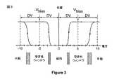
図3は、図1の干渉変調器についての可動反射層位置対印加電圧を示す図の一例を示している。MEMS干渉変調器の場合、行/列(すなわち、コモン/セグメント)書込みプロシージャが、図3に示すこれらのデバイスのヒステリシス特性を利用し得る。干渉変調器は、可動反射層すなわちミラーに緩和状態から作動状態に変更させるために、たとえば、約10ボルトの電位差を必要とし得る。電圧がその値から低減されると、電圧が低下して、たとえば、10ボルトより下に戻ったとき、可動反射層はそれの状態を維持するが、電圧が2ボルトより下に低下するまで、可動反射層は完全には緩和しない。したがって、図3に示すように、デバイスが緩和状態または作動状態のいずれかで安定する印加電圧のウィンドウがある、電圧の範囲、約3〜7ボルトが存在する。これは、本明細書では「ヒステリシスウィンドウ」または「安定性ウィンドウ」と呼ばれる。図3のヒステリシス特性を有するディスプレイアレイ30の場合、行/列書込みプロシージャは、一度に1つまたは複数の行をアドレス指定するように設計され得、その結果、所与の行のアドレス指定中に、作動されるべきアドレス指定された行におけるピクセルは、約10ボルトの電圧差にさらされ、緩和されるべきピクセルは、ほぼ0ボルトの電圧差にさらされる。アドレス指定後に、それらのピクセルは、それらが前のストローブ状態にとどまるように、約5ボルトの定常状態またはバイアス電圧差にさらされる。この例では、アドレス指定された後に、各ピクセルは、約3〜7ボルトの「安定性ウィンドウ」内の電位差を経験する。このヒステリシス特性の特徴は、たとえば図1に示した、ピクセル設計が、同じ印加電圧条件下で作動または緩和のいずれかの既存の状態で安定したままであることを可能にする。各IMODピクセルは、作動状態にあろうと緩和状態にあろうと、本質的に、固定反射層と可動反射層とによって形成されるキャパシタであるので、この安定状態は、電力を実質的に消費するかまたは失うことなしに、ヒステリシスウィンドウ内の定常電圧において保持されることができる。その上、印加電圧電位が実質的に固定のままである場合、電流は本質的にほとんどまたは全くIMODピクセルに流れ込まない。 FIG. 3 shows an example of a diagram illustrating movable reflective layer position versus applied voltage for the interferometric modulator of FIG. In the case of a MEMS interferometric modulator, a row / column (ie, common / segment) write procedure may take advantage of the hysteresis characteristics of these devices shown in FIG. An interferometric modulator may require, for example, a potential difference of about 10 volts to cause the movable reflective layer or mirror to change from a relaxed state to an activated state. When the voltage is reduced from that value, the voltage drops, for example, when it returns below 10 volts, the movable reflective layer maintains its state, but until the voltage drops below 2 volts, The movable reflective layer does not relax completely. Thus, as shown in FIG. 3, there is a voltage range, approximately 3-7 volts, where there is a window of applied voltage where the device is stable in either a relaxed state or an operational state. This is referred to herein as a “hysteresis window” or “stability window”. For the
いくつかの実装形態では、所与の行におけるピクセルの状態の所望の変化(もしあれば)に従って、列電極のセットに沿って「セグメント」電圧の形態のデータ信号を印加することによって、画像のフレームが作成され得る。フレームが一度に1行書き込まれるように、アレイの各行が順次アドレス指定され得る。第1の行におけるピクセルに所望のデータを書き込むために、第1の行におけるピクセルの所望の状態に対応するセグメント電圧が列電極上に印加されることができ、特定の「コモン」電圧または信号の形態の第1の行パルスが第1の行電極に印加されることができる。セグメント電圧のセットは次に、第2の行におけるピクセルの状態の所望の変化(もしあれば)に対応するように変更されることができ、第2のコモン電圧が第2の行電極に印加されることができる。いくつかの実装形態では、第1の行におけるピクセルは、列電極に沿って印加されたセグメント電圧の変化による影響を受けず、第1のコモン電圧行パルス中にそれらのピクセルが設定された状態にとどまる。このプロセスは、画像フレームを生成するために、一連の行全体、または代替的に、一連の列全体について、逐次方式で繰り返され得る。フレームは、何らかの所望の数のフレーム毎秒でこのプロセスを断続的に反復することによって、新しい画像データでリフレッシュおよび/または更新されることができる。 In some implementations, by applying a data signal in the form of a “segment” voltage along a set of column electrodes according to a desired change (if any) in the state of pixels in a given row, A frame can be created. Each row of the array can be addressed sequentially so that the frame is written one row at a time. In order to write the desired data to the pixels in the first row, a segment voltage corresponding to the desired state of the pixels in the first row can be applied on the column electrode, and a particular “common” voltage or signal A first row pulse of the form can be applied to the first row electrode. The set of segment voltages can then be changed to correspond to the desired change (if any) in the state of the pixels in the second row, and a second common voltage is applied to the second row electrode. Can be done. In some implementations, the pixels in the first row are unaffected by changes in the segment voltage applied along the column electrodes, and the pixels are set during the first common voltage row pulse. Stay on. This process may be repeated in a sequential manner for the entire series of rows, or alternatively for the entire series of columns, to generate an image frame. Frames can be refreshed and / or updated with new image data by intermittently repeating this process at some desired number of frames per second.
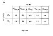
各ピクセルの両端間に印加されるセグメント信号とコモン信号の組合せ(すなわち、各ピクセルの両端間の電位差)が、各ピクセルの得られる状態を決定する。図4は、様々なコモン電圧およびセグメント電圧が印加されたときの干渉変調器の様々な状態を示す表の一例を示している。当業者によって容易に理解されるように、「セグメント」電圧は、列電極または行電極のいずれかに印加され得、「コモン」電圧は、列電極または行電極のうちの他方に印加され得る。 The combination of segment signal and common signal applied across each pixel (ie, the potential difference across each pixel) determines the resulting state of each pixel. FIG. 4 shows an example of a table showing various states of the interferometric modulator when various common voltages and segment voltages are applied. As readily understood by those skilled in the art, a “segment” voltage can be applied to either the column electrode or the row electrode, and a “common” voltage can be applied to the other of the column electrode or the row electrode.
図4に(ならびに図5Bに示すタイミング図に)示すように、開放電圧VCRELがコモンラインに沿って印加されたとき、コモンラインに沿ったすべての干渉変調器素子は、セグメントラインに沿って印加された電圧、すなわち、高いセグメント電圧VSHおよび低いセグメント電圧VSLにかかわらず、代替的に開放または非作動状態と呼ばれる、緩和状態に入れられることになる。特に、開放電圧VCRELがコモンラインに沿って印加されると、そのピクセルのための対応するセグメントラインに沿って高いセグメント電圧VSHが印加されたときも、低いセグメント電圧VSLが印加されたときも、変調器の両端間の潜在的な電圧(代替的にピクセル電圧と呼ばれる)は緩和ウィンドウ(図3参照。開放ウィンドウとも呼ばれる)内にある。As shown in FIG. 4 (as well as in the timing diagram shown in FIG. 5B), when an open circuit voltage VCREL is applied along the common line, all interferometric modulator elements along the common line will move along the segment line. applied voltage, i.e., regardless of the high segment voltage VSH and lower segment voltage VSL, is alternatively referred to as open or inoperative state, it will be taken into a relaxed state. In particular, when the open circuit voltage VCREL is applied along the common line, the low segment voltage VSL is also applied when the high segment voltage VSH is applied along the corresponding segment line for that pixel. Sometimes, the potential voltage across the modulator (alternatively called the pixel voltage) is within the relaxation window (see FIG. 3, also called the open window).
高い保持電圧VCHOLD_Hまたは低い保持電圧VCHOLD_Lのような保持電圧がコモンライン上に印加されたとき、干渉変調器の状態は一定のままであることになる。たとえば、緩和IMODは緩和位置にとどまることになり、作動IMODは作動位置にとどまることになる。保持電圧は、対応するセグメントラインに沿って高いセグメント電圧VSHが印加されたときも、低いセグメント電圧VSLが印加されたときも、ピクセル電圧が安定性ウィンドウ内にとどまることになるように、選択され得る。したがって、セグメント電圧スイング、すなわち、高いVSHと低いセグメント電圧VSLとの間の差は、正または負のいずれかの安定性ウィンドウの幅よりも小さい。When a holding voltage such as a high holding voltage VCHOLD_H or a low holding voltage VCHOLD_L is applied on the common line, the state of the interferometric modulator remains constant. For example, the relaxed IMOD will remain in the relaxed position and the activated IMOD will remain in the activated position. The holding voltage is such that the pixel voltage remains within the stability window when a high segment voltage VSH is applied along the corresponding segment line and when a low segment voltage VSL is applied. Can be selected. Therefore, the segment voltage swing, i.e., the difference between high VSH and lower segment voltage VSL, less than the positive or negative of the width of any of the stability window.
高いアドレス指定電圧VCADD_Hまたは低いアドレス指定電圧VCADD_Lのようなアドレス指定または作動電圧がコモンライン上に印加されたとき、それぞれのセグメントラインに沿ったセグメント電圧の印加によって、データがそのコモンラインに沿った変調器に選択的に書き込まれることができる。セグメント電圧は、作動が印加されたセグメント電圧に依存するように選択され得る。アドレス指定電圧がコモンラインに沿って印加されたとき、一方のセグメント電圧の印加は、安定性ウィンドウ内のピクセル電圧をもたらし、ピクセルが非作動のままであることを引き起こすことになる。対照的に、他方のセグメント電圧の印加は、安定性ウィンドウを越えるピクセル電圧をもたらし、ピクセルの作動をもたらすことになる。作動を引き起こす特定のセグメント電圧は、どのアドレス指定電圧が使用されるかに応じて変動することができる。いくつかの実装形態では、高いアドレス指定電圧VCADD_Hがコモンラインに沿って印加されたとき、高いセグメント電圧VSHの印加は、変調器がそれの現在位置にとどまることを引き起こすことができ、低いセグメント電圧VSLの印加は、変調器の作動を引き起こすことができる。当然の結果として、低いアドレス指定電圧VCADD_Lが印加されたとき、セグメント電圧の影響は反対であることができ、高いセグメント電圧VSHは変調器の作動を引き起こし、低いセグメント電圧VSLは変調器の状態に影響しない(すなわち、安定したままである)。When an addressing or actuation voltage such as a high addressing voltage VCADD_H or a low addressing voltage VCADD_L is applied on a common line, application of a segment voltage along each segment line causes data to be applied to that common line. Along the modulator can be selectively written. The segment voltage may be selected such that operation depends on the applied segment voltage. When an addressing voltage is applied along the common line, the application of one segment voltage will result in a pixel voltage within the stability window, causing the pixel to remain inactive. In contrast, application of the other segment voltage results in a pixel voltage that exceeds the stability window, resulting in pixel operation. The particular segment voltage that causes actuation can vary depending on which addressing voltage is used. In some implementations, when the high addressability voltage VCADD_H is applied along the common line, application of the high segment voltage VSH may cause the modulator remains in the current position of it, low Application of the segment voltage VSL can cause the modulator to operate. As a natural consequence, when a low addressing voltage VCADD_L is applied, the effect of the segment voltage can be reversed, a high segment voltage VSH causes the modulator to operate and a low segment voltage VSL is the modulator voltage. Does not affect the state of (ie remains stable).
いくつかの実装形態では、常に変調器の両端間で同じ極性電位差を引き起こす保持電圧、アドレス電圧、およびセグメント電圧が使用され得る。いくつかの他の実装形態では、変調器の電位差の極性を交番する信号が使用されることができる。変調器の両端間の極性の交番(すなわち、書込みプロシージャの極性の交番)は、単一の極性の反復書込み動作後に起こることがある電荷蓄積を低減または抑止し得る。 In some implementations, a holding voltage, an address voltage, and a segment voltage that always cause the same polarity potential difference across the modulator may be used. In some other implementations, a signal that alternates the polarity of the potential difference of the modulator can be used. The polarity alternation between the ends of the modulator (ie, the polarity alternation of the write procedure) may reduce or inhibit charge accumulation that may occur after a single polarity repetitive write operation.
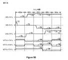
図5Aは、図2の3×3干渉変調器ディスプレイにおけるディスプレイデータのフレームを示す図の一例を示している。図5Bは、図5Aに示すディスプレイデータのフレームを書き込むために使用され得るコモン信号およびセグメント信号についてのタイミング図の一例を示している。それらの信号は、たとえば、図2の3×3アレイに印加されることができ、これは、図5Aに示すライン時間60eディスプレイ配置を最終的にもたらすことになるだろう。図5Aにおける作動知友の変調器は暗状態にあり、すなわち、その状態では、反射光の実質的部分が、たとえば、閲覧者に、暗い外観をもたらすように可視スペクトルの外にある。図5Aに示すフレームを書き込むより前は、ピクセルは任意の状態にあることができるが、図5Bのタイミング図に示す書込みプロシージャは、各変調器が、第1のライン時間60aの前に、開放されており、非作動状態に属すると仮定する。 FIG. 5A shows an example of a diagram illustrating a frame of display data in the 3 × 3 interferometric modulator display of FIG. FIG. 5B shows an example of a timing diagram for common and segment signals that may be used to write the frame of display data shown in FIG. 5A. Those signals, for example, can be applied to the 3 × 3 array of FIG. 2, which will ultimately result in the
第1のライン時間60a中に、開放電圧70がコモンライン1上に印加され、コモンライン2上に印加される電圧が、高い保持電圧72において始まり、開放電圧70に移動し、低い保持電圧76がコモンライン3に沿って印加される。したがって、コモンライン1に沿った変調器(コモン1,セグメント1)、(1,2)および(1,3)は、第1のライン時間60aの持続時間の間、緩和または非作動状態にとどまり、コモンライン2に沿った変調器(2,1)、(2,2)および(2,3)は、緩和状態に移動することになり、コモンライン3に沿った変調器(3,1)、(3,2)および(3,3)は、それらの前の状態にとどまることになる。図4を参照すると、コモンライン1、2または3のいずれも、ライン時間60a中に作動を引き起こす電圧レベルにさらされていないので(すなわち、VCREL−緩和、およびVCHOLD_L−安定)、セグメントライン1、2および3に沿って印加されたセグメント電圧は、干渉変調器の状態に影響しないことになる。During the
第2のライン時間60b中に、コモンライン1上の電圧は高い保持電圧72に移動し、コモンライン1に沿ったすべての変調器は、アドレス指定または作動電圧がコモンライン1上に印加されなかったので、印加されたセグメント電圧にかかわらず、緩和状態にとどまる。コモンライン2に沿った変調器は、開放電圧70の印加により、緩和状態にとどまり、コモンライン3に沿った変調器(3,1)、(3,2)および(3,3)は、コモンライン3に沿った電圧が開放電圧70に移動するとき、緩和することになる。 During the
第3のライン時間60c中に、コモンライン1は、コモンライン1上に高いアドレス電圧74を印加することによってアドレス指定される。このアドレス電圧の印加中に低いセグメント電圧64がセグメントライン1および2に沿って印加されるので、変調器(1,1)および(1,2)の両端間のピクセル電圧は変調器の正の安定性ウィンドウの上端よりも大きく(すなわち、電圧差は、あらかじめ定義されたしきい値を超えた)、変調器(1,1)および(1,2)は作動される。逆に、高いセグメント電圧62がセグメントライン3に沿って印加されるので、変調器(1,3)の両端間のピクセル電圧は、変調器(1,1)および(1,2)のピクセル電圧よりも小さく、変調器の正の安定性ウィンドウ内にとどまり、したがって変調器(1,3)は緩和したままである。また、ライン時間60c中に、コモンライン2に沿った電圧は低い保持電圧76に減少し、コモンライン3に沿った電圧は開放電圧70にとどまり、コモンライン2および3に沿った変調器を緩和位置のままにする。 During the
第4のライン時間60d中に、コモンライン1上の電圧は、高い保持電圧72に戻り、コモンライン1に沿った変調器を、それらのそれぞれのアドレス指定された状態のままにする。コモンライン2上の電圧は低いアドレス電圧78に減少される。高いセグメント電圧62がセグメントライン2に沿って印加されるので、変調器(2,2)の両端間のピクセル電圧は、変調器の負の安定性ウィンドウの下側端部を下回り、変調器(2,2)が作動することを引き起こす。逆に、低いセグメント電圧64がセグメントライン1および3に沿って印加されるので、変調器(2,1)および(2,3)は緩和位置にとどまる。コモンライン3上の電圧は、高い保持電圧72に増加し、コモンライン3に沿った変調器を緩和状態のままにする。次いで、コモンライン2上の電圧は、低い保持電圧76に遷移して戻る。 During the fourth line time 60d, the voltage on the
最後に、第5のライン時間60e中に、コモンライン1上の電圧は高い保持電圧72にとどまり、コモンライン2上の電圧は低い保持電圧76にとどまり、コモンライン1および2に沿った変調器を、それらのそれぞれのアドレス指定された状態のままにする。コモンライン3上の電圧は、コモンライン3に沿った変調器をアドレス指定するために、高いアドレス電圧74に増加する。低いセグメント電圧64がセグメントライン2および3上に印加されるので、変調器(3,2)および(3,3)は作動するが、セグメントライン1に沿って印加された高いセグメント電圧62は、変調器(3,1)が緩和位置にとどまることを引き起こす。したがって、第5のライン時間60eの終わりに、3×3ピクセルアレイは、図5Aに示す状態にあり、他のコモンライン(図示せず)に沿った変調器がアドレス指定されているときに起こり得るセグメント電圧の変動にかかわらず、保持電圧がコモンラインに沿って印加される限り、その状態にとどまることになる。 Finally, during the
図5Bのタイミング図では、所与の書込みプロシージャ(すなわち、ライン時間60a〜60e)は、高い保持およびアドレス電圧、または低い保持およびアドレス電圧のいずれかの使用を含むことができる。書込みプロシージャが所与のコモンラインについて完了されると(また、コモン電圧が、作動電圧と同じ極性を有する保持電圧に設定されると)、ピクセル電圧は、所与の安定性ウィンドウ内にとどまり、開放電圧がそのコモンライン上に印加されるまで、緩和ウィンドウを通過しない。さらに、各変調器が、変調器をアドレス指定するより前に書込みプロシージャの一部として開放されるので、開放時間ではなく変調器の作動時間が、必要なライン時間を決定し得る。詳細には、変調器の開放時間が作動時間よりも大きい実装形態では、開放電圧は、図5Bに示すように、単一のライン時間よりも長く印加され得る。いくつかの他の実装形態では、コモンラインまたはセグメントラインに沿って印加される電圧が、異なる色の変調器など、異なる変調器の作動電圧および開放電圧の変動を相殺するように変動し得る。 In the timing diagram of FIG. 5B, a given write procedure (ie,
上記に記載した原理に従って動作する干渉変調器の構造の詳細は大きく異なり得る。たとえば、図6A〜図6Eは、可動反射層14とそれの支持構造とを含む、干渉変調器の異なる実装形態の断面図の例を示している。図6Aは、金属材料のストリップ、すなわち、可動反射層14が、基板20から直角に延在する支持体18上に堆積される、図1の干渉変調器ディスプレイの部分断面図の一例を示している。図6Bでは、各IMODの可動反射層14は、概して形状が正方形または長方形であり、コーナーにおいてまたはその近くでテザー32に接して支持体に取り付けられる。図6Cでは、可動反射層14は、概して形状が正方形または長方形であり、フレキシブルな金属を含み得る変形可能層34から吊るされる。変形可能層34は、可動反射層14の外周の周りで基板20に直接または間接的に接続することができる。これらの接続は、本明細書では支持ポストと呼ばれる。図6Cに示す実装形態は、変形可能層34によって行われる可動反射層14の機械的機能からのそれの光学的機能の分離から派生する追加の利益を有する。この分離は、反射層14のために使用される構造設計および材料と、変形可能層34のために使用される構造設計および材料とが、互いとは無関係に最適化されることを可能にする。 The details of the structure of interferometric modulators that operate in accordance with the principles set forth above may vary widely. For example, FIGS. 6A-6E show examples of cross-sectional views of different implementations of interferometric modulators that include the movable
図6Dは、可動反射層14が反射副層14aを含む、IMODの別の例を示している。可動反射層14は、支持ポスト18などの支持構造上に載る。支持ポスト18は、たとえば、可動反射層14が緩和位置にあるとき、可動反射層14と光学スタック16との間にギャップ19が形成されるように、下側静止電極(すなわち、図示のIMODにおける光学スタック16の一部)からの可動反射層14の分離を可能にする。可動反射層14は、電極として働くように構成され得る伝導性層14cと、支持層14bとをも含むことができる。この例では、伝導性層14cは、基板20から遠位にある支持層14bの一方の面に配設され、反射副層14aは、基板20の近位にある支持層14bの他方の面に配設される。いくつかの実装形態では、反射副層14aは、伝導性であることがあり、支持層14bと光学スタック16との間に配設されることができ。支持層14bは、誘電材料、たとえば、酸窒化ケイ素(SiON)または二酸化ケイ素(SiO2)の、1つまたは複数の層を含むことができる。いくつかの実装形態では、支持層14bは、たとえば、SiO2/SiON/SiO23層スタックなど、複数の層のスタックであり得る。反射副層14aと伝導性層14cのいずれかまたは両方は、たとえば、約0.5%の銅(Cu)または別の反射金属材料を用いた、アルミニウム(Al)合金を含むことができる。誘電支持層14bの上および下で伝導性層14a、14cを採用することは、応力のバランスをとり、伝導の向上を与えることができる。いくつかの実装形態では、反射副層14aおよび伝導性層14cは、可動反射層14内の特定の応力プロファイルを達成することなど、様々な設計目的で、異なる材料から形成され得る。FIG. 6D shows another example of an IMOD in which the movable
図6Dに示すように、いくつかの実装形態はブラックマスク構造23をも含むことができる。ブラックマスク構造23は、周辺光または迷光を吸収するために、光学不活性領域において(たとえば、ピクセル間にまたはポスト18の下に)形成され得る。ブラックマスク構造23はまた、光がディスプレイの不活性部分から反射されることまたはそれを透過されることを抑止し、それによりコントラスト比を増加させることによって、ディスプレイデバイスの光学的特性を改善することができる。さらに、ブラックマスク構造23は、伝導性であり、電気的バス層として機能するように構成され得る。いくつかの実装形態では、行電極は、接続された行電極の抵抗を低減するために、ブラックマスク構造23に接続され得る。ブラックマスク構造23は、堆積およびパターニング技法を含む様々な方法を使用して形成され得る。ブラックマスク構造23は1つまたは複数の層を含むことができる。たとえば、いくつかの実装形態では、ブラックマスク構造23は、光吸収体として働くモリブデンクロム(MoCr)層と、SiO2層と、反射体およびバス層として働くアルミニウム合金と、を含み、それぞれ、約30〜80Å、500〜1000Å、および500〜6000Åの範囲内の厚さである。1つまたは複数の層は、たとえば、MoCr層およびSiO2層の場合は、カーボンテトラフルオロメタン(CF4)および/または酸素(O2)、ならびにアルミニウム合金層の場合は、塩素(Cl2)および/または三塩化ホウ素(BCL3)を含む、フォトリソグラフィおよびドライエッチングを含む、様々な技法を使用してパターニングされ得る。いくつかの実装形態では、ブラックマスク23はエタロンまたは干渉スタック構造であり得る。そのような干渉スタックブラックマスク構造23では、伝導性吸収体は、各行または列の光学スタック16における下側静止電極間で信号を送信するかまたは信号をバスするために使用され得る。いくつかの実装形態では、スペーサ層35が、概して、ブラックマスク23中の伝導性層から吸収層16aを電気的に絶縁するのに、役立つことができる。Some implementations may also include a
図6Eは、可動反射層14が自立している、IMODの別の例を示している。図6Dとは対照的に、図6Eの実装形態は支持ポスト18を含まない。代わりに、可動反射層14は、複数のロケーションにおいて、下にある光学スタック16に接触し、可動反射層14の湾曲は、干渉変調器の両端間の電圧が作動を引き起こすには不十分であるとき、可動反射層14が図6Eの非作動位置に戻るという、十分な支持を与える。複数のいくつかの異なる層を含んでいることがある光学スタック16は、ここでは明快のために、光吸収体16aと誘電体16bとを含む状態で示されている。いくつかの実装形態では、光吸収体16aは、固定電極としても、部分反射層としても働き得る。 FIG. 6E shows another example of an IMOD in which the movable
図6A〜図6Eに示す実装形態などの実装形態では、IMODは直視型デバイスとして機能し、直視型デバイスでは、画像が、透明基板20の正面、すなわち、変調器が配置された面の反対の面から、閲覧される。これらの実装形態では、デバイスの背面部分(すなわち、たとえば、図6Cに示す変形可能層34を含む、可動反射層14の背後のディスプレイデバイスの任意の部分)は、反射層14がデバイスのそれらの部分を光学的に遮蔽するので、ディスプレイデバイスの画質に影響を及ぼすことまたは悪影響を及ぼすことなしに、構成され、作用され得る。たとえば、いくつかの実装形態では、バス構造(図示せず)が可動反射層14の背後に含まれ得、これは、電圧アドレス指定およびそのようなアドレス指定に起因する移動など、変調器の電気機械的特性から変調器の光学的特性を分離する能力を与える。さらに、図6A〜図6Eの実装形態は、パターニングなどの処理を簡略化することができる。 In implementations such as the implementations shown in FIGS. 6A-6E, the IMOD functions as a direct view device where the image is opposite the front of the
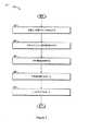
図7は、干渉変調器のための製造プロセス80を示す流れ図の一例を示しており、図8A〜図8Eは、そのような製造プロセス80の対応する段階の断面概略図の例を示している。いくつかの実装形態では、製造プロセス80は、図7に示されていない他のブロックに加えて、たとえば、図1および図6に示す一般的なタイプの干渉変調器を製造するために実装され得る。図1、図6および図7を参照すると、プロセス80は、基板20上での光学スタック16の形成を伴うブロック82において開始する。図8Aは、基板20上で形成されたそのような光学スタック16を示している。基板20は、ガラスまたはプラスチックなどの透明基板であり得、それは、フレキシブルであるかまたは比較的固く曲がらないことがあり、光学スタック16の効率的な形成を可能にするために、事前準備プロセス、たとえば、洗浄にかけられていることができる。上記で説明したように、光学スタック16は、電気伝導性であり、部分的に透明で、部分的に反射性であることができ、たとえば、透明基板20上に、所望の特性を有する1つまたは複数の層を堆積させることによって、作製され得る。図8Aでは、光学スタック16は、副層16aおよび16bを有する多層構造を含むが、いくつかの他の実装形態では、より多いまたはより少ない副層が含まれ得る。いくつかの実装形態では、副層16a、16bのうちの1つは、組み合わせられた導体/吸収体副層16aなど、光吸収特性と伝導特性の両方で構成され得る。さらに、副層16a、16bのうちの1つまたは複数は、平行ストリップにパターニングされ得、ディスプレイデバイスにおける行電極を形成し得る。そのようなパターニングは、当技術分野で知られているマスキングおよびエッチングプロセスまたは別の好適なプロセスによって実行され得る。いくつかの実装形態では、副層16a、16bのうちの1つは、1つまたは複数の金属層(たとえば、1つまたは複数の反射層および/または伝導性層)上で堆積された副層16bなど、絶縁層または誘電体層であり得る。さらに、光学スタック16は、ディスプレイの行を形成する個々の平行ストリップにパターニングされ得る。 FIG. 7 shows an example of a flow diagram illustrating a
プロセス80はブロック84において続き、光学スタック16上での犠牲層25の形成を伴う。犠牲層25は、キャビティ19を形成するために後で(たとえば、ブロック90において)除去され、したがって、犠牲層25は、図1に示した得られた干渉変調器12には示されていない。図8Bは、光学スタック16上で形成された犠牲層25を含む、部分的に作製されたデバイスを示している。光学スタック16上での犠牲層25の形成は、後続の除去後に、所望の設計サイズを有するギャップまたはキャビティ19(図1および図8Eも参照)を与えるように選択された厚さの、モリブデン(Mo)またはアモルファスシリコン(Si)など、フッ化キセノン(XeF2)エッチング可能材料の堆積を含み得る。犠牲材料の堆積は、物理蒸着(PVD、たとえば、スパッタリング)、プラズマ強化化学蒸着(PECVD)、熱化学蒸着(熱CVD)、またはスピンコーティングなど、堆積技法を使用して行われ得る。
プロセス80はブロック86において続き、支持構造、たとえば、図1、図6および図8Cに示すポスト18の形成を伴う。ポスト18の形成は、支持構造開口を形成するために犠牲層25をパターニングすることと、次いで、PVD、PECVD、熱CVD、またはスピンコーティングなど、堆積方法を使用して、ポスト18を形成するために開口中に材料(たとえば、ポリマまたは無機材料、たとえば、酸化ケイ素)を堆積させることとを含み得る。いくつかの実装形態では、犠牲層中に形成された支持構造開口は、ポスト18の下側端部が図6Aに示すように基板20に接触するように、犠牲層25と光学スタック16の両方を貫いて、下にある基板20まで延在することがある。代替的に、図8Cに示すように、犠牲層25中に形成された開口は、犠牲層25は通るが、光学スタック16は通らないで、延在することがある。たとえば、図8Eは、光学スタック16の上側表面と接触している支持ポスト18の下側端部を示している。ポスト18、または他の支持構造は、犠牲層25上で支持構造材料の層を堆積させることと、犠牲層25中の開口から離れて配置された支持構造材料の部分をパターニングすることとによって形成され得る。支持構造は、図8Cに示すように開口内に配置され得るが、少なくとも部分的に、犠牲層25の一部分の上で延在することもある。上述のように、犠牲層25および/または支持ポスト18のパターニングは、パターニングおよびエッチングプロセスによって実行され得るが、代替エッチング方法によっても実行され得る。
プロセス80はブロック88において続き、図1、図6および図8Dに示す可動反射層14などの可動反射層または膜の形成を伴う。可動反射層14は、1つまたは複数のパターニング、マスキング、および/またはエッチングステップとともに、1つまたは複数の堆積ステップ、たとえば、反射層(たとえば、アルミニウム、アルミニウム合金)堆積を採用することによって、形成され得る。可動反射層14は、電気伝導性であり、電気伝導性層と呼ばれることができる。いくつかの実装形態では、可動反射層14は、図8Dに示すように複数の副層14a、14b、14cを含み得る。いくつかの実装形態では、副層14a、14cなど、副層のうちの1つまたは複数は、それらの光学的特性のために選択された高反射性副層を含み得、別の副層14bは、それの機械的特性のために選択された機械的副層を含み得る。犠牲層25は、ブロック88において形成された部分的に作製された干渉変調器中に依然として存在するので、可動反射層14は、一般にこの段階では可動でない。犠牲層25を含んでいる部分的に作製されたIMODは、本明細書では「非開放」IMODと呼ばれることもある。図1に関して上記で説明したように、可動反射層14は、ディスプレイの列を形成する個々の平行ストリップにパターニングされ得る。
プロセス80はブロック90において続き、キャビティ、たとえば、図1、図6および図8Eに示すキャビティ19の形成を伴う。キャビティ19は、(ブロック84において堆積された)犠牲材料25をエッチャントにさらすことによって形成され得る。たとえば、MoまたはアモルファスSiなどのエッチング可能犠牲材料が、ドライ化学エッチングによって、たとえば、一般に、キャビティ19を囲む構造に対して選択的に除去される、所望の量の材料を除去するのに有効である時間期間の間、固体XeF2から派生した蒸気などの気体または蒸気エッチャントに犠牲層25をさらすことによって、除去され得る。他のエッチング方法、たとえば、ウェットエッチングおよび/またはプラズマエッチングも使用され得る。犠牲層25がブロック90中に除去されるので、可動反射層14は、一般に、この段階後に可動となる。犠牲材料25の除去後に、得られた完全にまたは部分的に作製されたIMODは、本明細書では「開放」IMODと呼ばれることができる。
本明細書で説明するいくつかの実装形態では、複合センサデバイスの少なくとも一部が、ディスプレイ上にオーバレイされるかまたはさもなければディスプレイと組み合わされることができ、カバーガラス装置に組み込まれ得る。カバーガラス装置は、2つ、3つまたはそれ以上の層を有し得る。いくつかの実装形態では、カバーガラス装置は、実質的に透明でフレキシブルな上側基板と、実質的に透明で比較的より堅い下側基板と、を含み得る。カバーガラスは、電極、実質的に透明なエラストマ層および/または力感知抵抗器材料など、基板上におよび/または基板間に配設された中間層を含み得る。いくつかのそのような実装形態では、カバーガラス装置の下側基板はディスプレイ基板上にオーバレイされ得る。 In some implementations described herein, at least a portion of the composite sensor device can be overlaid on the display or otherwise combined with the display and incorporated into the cover glass apparatus. Cover glass devices can have two, three or more layers. In some implementations, the cover glass device may include a substantially transparent and flexible upper substrate and a substantially transparent and relatively stiffer lower substrate. The cover glass may include an intermediate layer disposed on and / or between the substrates, such as electrodes, substantially transparent elastomer layers, and / or force sensitive resistor materials. In some such implementations, the lower substrate of the cover glass device can be overlaid on the display substrate.
図9Aは、カバーガラス装置の基板上に形成されたセンサ電極の一例を示している。図9Aに示す例では、ダイヤモンド形の実質的に透明な電極の3つの行915が、実質的に透明な上側基板905上に示されており、実質的に透明なダイヤモンド形の電極の7つの列920が、実質的に透明な下側基板910上に配置されている。説明のために、ここでは比較的少数の行および列しか示されていないが、実際のセンサデバイスでは、行および列の数は、数十から数百さらには千以上に及び得る。行と列は大部分は交換可能であり、ここではいかなる限定も意図されていないことに気づくであろう。いくつかの実装形態では、複合センサデバイス900の上側基板905は、フレキシブルポリマなどの比較的フレキシブルな材料から形成され得る。いくつかのそのような例では、上側基板905は、ポリエチレンテレフタラート(PET)、ポリエチレンナフタレート(PEN)、ポリイミド、または同様の材料から製作された、クリアなプラスチック膜であり得る。いくつかの実装形態では、上側基板905は、0.5〜5GPaの範囲内の弾性率を有し得る。下側基板910は、ガラス、プラスチック、ポリマなどから形成され得る。いくつかの実装形態では、下側基板910はディスプレイ基板であり得る。たとえば、いくつかの実装形態では、下側基板910は、上記で説明した透明基板20と同じ基板であり得る。 FIG. 9A shows an example of the sensor electrode formed on the substrate of the cover glass device. In the example shown in FIG. 9A, three
この例では、1つおきの列電極920は、重複領域925aにおける行電極915の対応するダイヤモンドの直下に配置されたダイヤモンド電極を含む。いくつかの実装形態は、行電極915のダイヤモンドと列電極920のダイヤモンドとのオフセットを有し、それにより、行電極915中のダイヤモンドと列920中のダイヤモンドとは、互いの上に部分的に重なる。 In this example, every
いくつかの実装形態では、行電極915および/または列電極920は、正方形、矩形、三角形、円形、卵形、等々のような他の形状に、およびフレーム、リング、または一連の接続された線分のような形状の中央の大部分が開いた領域を含む形状に、形成され得る。いくつかのそのような形状の説明は、その内容の全文が参照により本明細書に組み込まれる、2010年12月21日に出願され、「Capacitive Touch Sensing Devices and Methods of Manufacturing Thereof」と題する係属中の米国特許出願第12/957,025号の様々な部分(たとえば、図11A〜図11Jおよび対応する説明を参照)中に含まれている。その上、別の実装形態では、行電極915が下側基板910上に形成され得、列電極920が上側基板905上に形成され得る。行電極915と列電極920との間に配置された圧縮性材料1025を含む、図10Cおよび図10Dを参照しながら以下で説明するような、いくつかの実装形態では、軽いタッチが、隣接するダイヤモンド間の相互キャパシタンスの変化を測定することによって、検出され得る(投影容量性タッチ(PCT)とも呼ばれる)。そのような実装形態では、上側基板905が押下されたとき、行電極915と列電極920との間のキャパシタンスの変化を測定することによって、スタイラスとの接触が検出され得る。 In some implementations, the
行電極915と列電極920との間にパターニングされた誘電材料を有する実装形態では、ギャップが、対応する行電極915と列電極920との間に形成され得る。そのような実装形態では、行電極915と列電極920との間の実効平行プレートキャパシタンスの変化によって(図10B参照)、または行電極915と列電極920とが直接機械的および電気的に接触したときに起こる抵抗の変化を測定することによって(図10A参照)、あるいは、指、スタイラス先端、指の稜線(ridge)などで押圧されたときの、行電極915と列電極920との間に配置された力感知抵抗器における変化を測定することによって(図10D参照)、隣接する電極間のPCT測定で軽いタッチが検出されることができ、また、スタイラス押下が検出されることができる。力感知抵抗器は、手書きおよびタッチセンサゾーン1005中で、指紋センサゾーン1010中で、またはその両方で、行電極915と列電極920との間に含まれ得る。いくつかのそのような実装形態では、高抵抗層が、スタイラスのロケーションの感知中、寄生信号の影響を最小限に抑えるために、行電極915または列電極920上に形成され得る。 In implementations having a dielectric material patterned between the
図9Bは、カバーガラス上に形成されたセンサ電極の別の例を示している。図9Bに示す例では、行電極915のダイヤモンドの下にダイヤモンドがあった列電極920は、デザインから削除されている。オーミック膜スイッチ、抵抗膜スイッチ、力感知抵抗性(FSR:force-sensitive resistive)材料を用いた抵抗スイッチ、固定直列抵抗器を用いたFSRスイッチ、または複合センサデバイス900の容量膜が、スタイラス接触、および場合によっては、指先または指の稜線を検出するために、行電極915と列電極920との間の交差部に(重複領域925bにおいて)形成され得る。そのような実装形態は、同じ列が、PCT方法によって軽いタッチを検出するという目的、あるいはキャパシタンス変化方法または抵抗変化方法のいずれかによってスタイラス接触を検出するという目的をはたすことができるので、外部処理回路に接続される必要がある列電極920の数を低減することができる(図9Bの列電極920および関連する接続パッドの数が、図9Aの列電極920および接続パッドよりも少数であることに留意されたい)。 FIG. 9B shows another example of the sensor electrode formed on the cover glass. In the example shown in FIG. 9B, the
たとえば、タッチモードでは、タッチを登録するために極めて軽い力しか必要とされなくても良い。しかしながら、手書きモードでは、センサは、ポインティングデバイスが通電しているか通電していないかにかかわらず、多くの形態のスタイラス、ペン、または他のポインタ入力を受け付けるように構成され得る。本明細書で説明するいくつかの実装形態は、指紋センサモードで動作する間は指紋を読み取るときに、また、手書きセンサモードで動作するときは不注意による手のひらタッチを検出および拒否するときに、起こり得るような、多数のマルチタッチイベントを同時に区別することが可能なセンサを与える。 For example, in the touch mode, only a very light force may be required to register a touch. However, in handwriting mode, the sensor may be configured to accept many forms of stylus, pen, or other pointer input, whether or not the pointing device is energized. Some implementations described herein detect fingerprints while operating in fingerprint sensor mode, and detect and reject inadvertent palm touches when operating in handwritten sensor mode. It provides a sensor capable of simultaneously distinguishing multiple multi-touch events as may occur.
図10Aは、複合センサデバイスの断面図の一例を示している。図10Aに示すセンサアレイは、組合せタッチ、スタイラス、および指紋センサとして示されているが、図10Aの構成および以下で説明する他の構成が、単にタッチセンサ、スタイラスセンサ、指紋センサとして、またはそれらの組合せとして働き得ることに留意されたい。図10Aに示す例では、2つの反復セルが、手書きおよびタッチセンサゾーン1005と呼ばれる第1の領域に示されている。そのような感知素子は、本明細書では「センセル」と呼ばれることもある。指紋センサゾーン1010と呼ばれる随意の第2の領域は、概して、指紋検出のためにしばしば必要とされる、より高い分解能を可能にするために電極間のより細かいピッチを有している。本明細書の他の場所で言及するように、いくつかの実装形態では、指紋センサと手書きおよびタッチセンサとは、異なるゾーン中にない。図10B〜図10Dは、別の複合センサデバイスの断面図の例を示している。図10A〜図10Dは、本明細書で与える多くの他の図面のように、一定の縮尺で描かれていないことがある。タッチ、手書き、および指紋ゾーンが図10A〜図10Dに示されているが、すべてのゾーンが通常同時にアクティブにされることになるとは限らない。また、すべてのゾーンおよび動作モードが、センサデバイス中で利用可能であるとは限らないこともある。1つまたは複数の指を使用してシングルタッチまたはマルチタッチすることが、手書きおよびタッチセンサゾーン1005中でPCTを使用して感知されるものとして示されており、手書きおよびタッチセンサゾーン1005では、特に軽いタッチ、ならびに適度のタッチおよび重いタッチが検出され得る。図10Aに示す例では、指1047の近接が上側電極1015と下側電極1030bとの間の電界1050を変え、相互キャパシタンスの変化を引き起こす。この影響は、関連する回路図1055aの可変キャパシタによって概略的に示されている。いくつかの実装形態では、上側電極1015は行電極であり得、上述のように、いくつかの他の実装形態では、上側電極1015は列電極であり得る(図9Aおよび図9B参照)。 FIG. 10A shows an example of a cross-sectional view of a composite sensor device. Although the sensor array shown in FIG. 10A is shown as a combined touch, stylus, and fingerprint sensor, the configuration of FIG. 10A and other configurations described below are simply touch sensors, stylus sensors, fingerprint sensors, or Note that it can work as a combination of In the example shown in FIG. 10A, two repetitive cells are shown in a first region called handwriting and
(ペン、ペンシル、またはポインタなど、スタイラスの先端が複合センサデバイス900の表面に対して押圧されたときに生じるような)大きい力または高い局所圧力は、オーミック膜スイッチまたは抵抗膜スイッチを用いて検出され得る。一例が図10Aに示されており、ペンまたはスタイラス1042によって引き起こされた高い局所圧力が、上側電極1015と下側電極1030aとを含む機械スイッチによって検出されることができる。固定抵抗器としばしば呼ばれる抵抗器1035が、上側電極1015と下側電極1030aとの直接短絡を防ぐために、上側電極1015と下側電極1030aとの間に配置され得る。垂直または蛇行固定抵抗器を含むスイッチが、回路図1055aにおいて概略的に表されている。抵抗器1035は、それと上側電極1015との間の電気的接触を助けるために、その上に配設された追加の金属層(図示せず)を有し得る。ここで定義されるような抵抗膜スイッチは、各センセルにおいて少なくとも固定抵抗器を含む(抵抗膜スイッチは、固定抵抗器と直列のまたは固定抵抗器の代わりの力感知抵抗器をも含み得る)が、オーミック膜スイッチは、上側電極および下側電極と直列の追加の固定抵抗器を必要としない。いくつかの実装形態では、固定抵抗器は、オーミック材料から形成され得る。いくつかの他の実装形態では、固定抵抗器は、電流の流れに対して比較的高い抵抗を与える漏れダイオード(leaky diode)または他のデバイスなど、非線形デバイスであり得る。固定抵抗器は、伝導性接触表面として働く、薄膜伝導性キャップを含み得る。デジタル抵抗タッチ(DRT)下側電極1030aとPCT下側電極1030bとを用いた1対1の対応が図10Aに示されているが、いくつかの構成では、PCT下側電極1030bは、1つまたは複数の隣接するセンセルにまたがっても良い。いくつかの構成では、PCT下側電極1030bは、DRT下側電極1030aよりも幅広く長い。 A large force or high local pressure (such as occurs when the tip of a stylus, such as a pen, pencil, or pointer) is pressed against the surface of the
いくつかの実装形態では、上側電極1015と下側電極1030aは、上記で説明した機械スイッチの代わりに、変形可能な平行プレートキャパシタの2つのプレートを形成するように構成され得る。いくつかの実装形態では、電極1015と電極1030aは、図10Bのエリア1065に示すように、エアギャップによって分離され得、通常の非押圧状態においてベースラインキャパシタンスに対応する間隔を有し得る。力または圧力が加えられると、上側電極1015は変位され、電極1015と電極1030aは近づく。電極1015と電極1030aとの間の電極間距離が低減されたとき、キャパシタンスは変化し(たとえば、増加し)、変位のアナログ変化の感知を可能にし、加えられた力または圧力の存在の推測を可能にする。したがって、ペン、スタイラス、等々からの高い局所圧力または力は、上側電極1015と下側電極1030aとの間の平行プレートキャパシタンス変化を介して検出され得る。圧力のそのような局所変化によって生じるキャパシタンス変化は、回路図1055bの可変キャパシタ1056によって概略的に表されている。示される構成では、固定抵抗器1035は、可変キャパシタ1056と直列である。他の構成(図示せず)では、固定抵抗器1035は省略され得る。 In some implementations, the
いくつかの実装形態では、中間層分離部(interlayer separation)1032が、上側電極と下側電極との間に圧縮性層1025を配設することによって、上側基板905と下側基板910との間に形成され得る。いくつかの実装形態では、圧縮性層1025は、エラストマのような、低い弾性率を有する、パターニング可能な薄い(たとえば、1〜10マイクロメータ)ポリマであり得る。いくつかのそのような実装形態では、圧縮性層1025は、上側基板905がペン、スタイラス、指、等々のタッチによって押下され、上側電極1015と下側電極1030aとの間の距離が変化したとき、キャパシタンス変化の直接測定を可能にし得る。圧縮性層1025は、上側基板905よりも低い弾性率を有し得る。たとえば、上側基板905は、PET、PEN、ポリイミド、または0.5〜5GPaの範囲内の弾性率を有する同様の材料から製作された、クリアなプラスチック膜であり得る。圧縮性層1025は、0.5〜50MPaの範囲内など、著しく低い弾性率を有し得る。 In some implementations, an
いくつかの実装形態では、圧縮性層1025は、上側基板905と下側基板910との間の空間または空隙(本明細書では「エアギャップ」と呼ばれることもある)を含むようにパターニングされ得る。図10Aおよび図10Bに示す実装形態など、いくつかの実装形態は、圧縮性層1025が上側電極1015と下側電極1030aとの間に形成されないエリア1065では空隙を含む。しかしながら、これらの例では、圧縮性層1025は、エリア1070では、上側基板905と下側電極1030bとの間に、空隙無しに延在する。いくつかのそのような実装形態によれば、圧縮性層1025は、エリア1065および1080にエアギャップがあるようにパターニングされ得る。圧縮性層1025領域の示された厚さおよび間隔は、例として示されているに過ぎない。エリア1065および1080中のエアギャップのロケーションおよび横寸法は、当業者が容易に理解するように、力感度、信頼性および/または光学的性能の所望のパラメータに従って選択され得る。たとえば、中間層分離部1032は、数分の1マイクロメータ〜数マイクロメータであり得る。エリア1065および1080中のエアギャップの厚さも、数分の1マイクロメータ〜数マイクロメータ厚であり得る。隣接する上側電極1015(隣接するセンセル)間のピッチまたは間隔は、手書きおよびタッチセンサゾーン1005中で10分の数ミリメートルから5ミリメートル超に及び得(下側電極1030aと下側電極1030bとの間のピッチは、それの約1/2)、これに対し、指紋センサゾーン1010中の隣接する電極1040間のピッチまたは間隔は、50マイクロメータほどと同じくらい小さいことがあり得る。 In some implementations, the
圧縮性層1025は、上側基板905の測定可能なたわみを可能にするのを助け得る。いくつかの実装形態では、圧縮性層1025はまた、図10Cに示し、以下で説明するように、エリア1065中にも形成され得る。いくつかのそのような実装形態では、圧縮性層1025は、上側基板905がペン、スタイラス、指、等々のタッチによって押下され、上側電極1015と下側電極1030aとの間の距離が変化したとき、キャパシタンス変化の直接測定を可能にする、エラストマ材料(または同様の材料)を含み得る。代替的に、上側電極1015と横方向に変位された下側電極1030bとの間の相互キャパシタンスも、ペン、スタイラス、指、等々の検出を可能にするために、変化し得る。 The
指紋センサゾーン1010は、指紋検出のために構成され得る。図10Aに示す実装形態では、上側指紋電極1020と下側指紋電極1040は、抵抗膜スイッチのアレイを形成し、抵抗膜スイッチのうちの1つが回路図1060aにおいて概略的に表されている。図10A〜図10Cに示す例では、圧縮性層1025は、エリア1080中で上側指紋電極1020と下側指紋電極1040との間に形成されない。しかしながら、(以下でより詳細に説明されることになる)図10Dに示す実装形態では、圧縮性層1025は、FSR材料1085が配置された領域を除いて、エリア1080中に形成される。 The
図10A〜図10Dに示す例では、上側指紋電極1020および下側指紋電極1040は、指紋センサゾーン1010中で比較的より高い分解能を与えるために、手書きおよびタッチセンサゾーン1005中の上側電極1015および下側電極1030のピッチよりも小さいピッチを有する。しかしながら、いくつかの代替実装形態では、上側指紋電極1020および下側指紋電極1040のピッチは、手書きおよびタッチセンサゾーン1005中の上側電極1015および下側電極1030のピッチと実質的に同じであっても良い。 In the example shown in FIGS. 10A-10D, the
圧縮性層1025は、リソグラフィおよびエッチング技法(または他のリソグラフィベースの技法)を使用してパターニングされ得る。いくつかの実装形態では、圧縮性層1025は、(この例では上側基板905の上表面である)センサの外表面に好適な力が加えられるまで、エリア1065および1080のオーミックスイッチまたは抵抗スイッチを開いたままにしておくことができる。圧縮性層1025は、ディスプレイをオーバレイするであろうセンサの一部であるので、圧縮性層1025は、実質的に透明であることかできる。 The
いくつかの実装形態では、圧縮性層1025は、下側基板910および上側基板905の屈折率に厳密に一致した屈折率を有し得る。いくつかの実装形態では、圧縮性層1025は、5%未満だけ、10%未満だけ、20%未満だけ、等々、下側基板910および上側基板905の屈折率とは異なる屈折率を有し得る。たとえば、屈折率の6%以下の差が、材料スタックを通る透過の0.2%未満の低減をもたらし得る。そのような実装形態は、圧縮性層1025が上側基板905から下側基板910まで延在するエリア中で、良好な光透過を与えることができる。しかしながら、光透過は、エアギャップ領域において低減され得、これは、空気と材料との各界面における反射によって引き起こされる。そのような反射は、式1において、上側基板905の屈折率(これは、近似的にn=約1.5であり得る)と空気の屈折率(no=1)とを使用して計算されるように、たとえば、4%よりも大きいことがあり得る。In some implementations, the
(n−no)2/(n+no)2=R (式1)
但し、Rは反射率である。(N−no )2 / (n + no )2 = R (Formula 1)
However, R is a reflectance.
したがって、最小横寸法のエアギャップを有する実装形態は、より良い光学的性能を与えることができる。しかしながら、いくつかのそのような実装形態は、所与の圧力に対してより少ないたわみをもたらし得、したがって圧力または加えられた力にあまり感知でないことがあり得る。 Thus, implementations having the smallest lateral dimension air gap can provide better optical performance. However, some such implementations may result in less deflection for a given pressure and therefore may be less sensitive to pressure or applied force.
よって、いくつかの実装形態は、光学的性能を改善することができる、屈折率の一致した(index-matched)圧縮性層1025を与える。エリア1065中でエアギャップを有するいくつかの実装形態においてさえ、手書きおよびタッチセンサゾーン1005の比較的小さい部分をエリア1065に占有させるアーキテクチャにより、光学的性能はすでに極めて良好であり得る。たとえば、エアギャップを有するエリア1065は、総面積の約50%未満を占有し得るが、他の例では、エリア1065は、総面積の約10%未満を占有し得る。そのような実装形態では、センサエリアの大部分は、エアギャップを有しないことになり、したがって、層905/層1025および層1025/層910の界面において、はるかに低減された反射、すなわち、両方の界面についての全反射が、式1に従って推定されるように<<1%であり得るような、反射を示すことになる。 Thus, some implementations provide an index-matched
個々の感知素子の、ペン、スタイラス、または指からの圧力または力に対する感度は(それらの感知素子が抵抗スイッチモードで使用されるのか変形可能平行プレートキャパシタモードで使用されるのかにかかわらず)、図11A〜図11Dに示すように、低弾性率圧縮性層1025を使用することにより、増加され得る。低弾性率圧縮性層1025は、より高い弾性率の材料によって課されることができるクランプ境界条件(clamped boundary condition)を除外し得る。低弾性率圧縮性層1025を有することは、スタイラス先端1105によってたわまされた圧縮性層1025のエリア1110の直径を効果的に増加させ、それによりエリア1110における上側基板905のたわみを増加させることができる。 The sensitivity of individual sensing elements to pressure or force from a pen, stylus, or finger (regardless of whether they are used in resistive switch mode or deformable parallel plate capacitor mode) It can be increased by using a low modulus
図11A〜図11Dは、高弾性率圧縮性層および低弾性率圧縮性層を有する複合センサデバイスの断面図の例を示している。図11Aは、圧縮性層1025aが、上側基板905と下側基板910との間にはさまれたパターニングされた高弾性率材料である、簡略化された組合せタッチ、手書き、および指紋センサの一部分のフレキシブル上側基板905と接触しているスタイラス先端1105を示している。圧縮性層1025a中のエアギャップ1115は、複合センサデバイス900の上側基板905が、加えられた力に伴って変形することを可能にするが、得られるたわまされたエリア1110は、比較的固い圧縮性層1025a中の小さいエアギャップ1115によって、部分的に制限される。 11A to 11D show examples of cross-sectional views of a composite sensor device having a high elastic modulus compressible layer and a low elastic modulus compressible layer. FIG. 11A shows a portion of a simplified combined touch, handwriting, and fingerprint sensor in which the
図11Bは、比較的よりフレキシブルな上側基板905と比較的あまりフレキシブルでない下側基板910との間にはさまれた低弾性率圧縮性層1025bを示している。この例では、スタイラスの力による上側基板905のたわまされたエリア1110は、スタイラス先端1105が上側基板905の外表面に対して押圧されるにつれて圧縮および変形する圧縮性層1025bの能力により、より大きい。図11Cに示す例では、スタイラス1105は、フレキシブル上側基板905が下側基板910との物理的接触を行う(または、ほぼ行う)のに十分に強く押圧されている。 FIG. 11B shows a low modulus
また、低弾性率エラストマ圧縮性層1025bの使用は、図11Dに示すように、行電極または列電極のピッチを減少させることなしに、加えられた圧力または力による横方向分解能を効果的に増加させ得る。スタイラス先端1105の先端が圧縮性層1025中のエアギャップ1115の直上にないときであっても、上側基板905の明らかなたわみが生じ、したがって、複合センサデバイス900が、隣接する感知素子間の比較的広い間隔を有する場合でも、スタイラス先端1105の検出を可能にすることができる。たとえば、隣接する行または列の間のピッチが0.5mmである場合でも、隣接するセンセルからの応答を平均化することによって、0.2mmの分解能で手書きが解像され得る。隣接する行または列の間の比較的より大きいピッチを可能にすることによって、そのような構成は、所与の分解能に対する行電極および列電極の総数の低減を可能にし、それにより手書きセンサコントローラ上のI/Oの数を低減し得る。この低減は、リードアウトの数を低減し、手書きコントローラのコストおよび複雑さを低減することができる。 Also, the use of a low modulus elastomer
複合センサの別の実装形態が、図10Cに示されている。図10Aおよび図10Bに示す実装形態と比較して、エアギャップは手書きおよびタッチセンサゾーン1005のエリア1065から削除されている。したがって、手書きおよびタッチセンサゾーン1005の光学的性能は、図10Aおよび図10Bに示す複合センサデバイス900の実装形態に対して向上され得る。図10Cに示す複合センサデバイス900の実装形態における手書きセンサは、可変平行プレートキャパシタとして機能し、平行プレートキャパシタンスの変化から上側層の重いタッチまたはたわみが検出される。この機能は、回路図1055cの可変キャパシタ1056によって表されている。 Another implementation of a composite sensor is shown in FIG. 10C. Compared to the implementation shown in FIGS. 10A and 10B, the air gap has been removed from
図10Dは、別の実装形態の別の例を示している。図10Dに示す例では、エアギャップは、指紋センサゾーン1010のエリア1080中で削除され、市販のFSR材料1085と置き換えられている。FSR材料1085は、圧縮されていないときは比較的高い値の抵抗を与え、圧縮されたときは比較的低い値の抵抗を与え、それにより、直接接触領域なしにもかかわらずスイッチとして機能する。この機能は、回路図1060bの可変抵抗器1087によって表されている。垂直抵抗器または蛇行抵抗器などの固定抵抗器1045が、各センセルにおいてFSR材料1085と直列に含まれ得る。透明な粒子または低フィルレシオ(fill ratio)の粒子のいずれかを含む透明なFSR材料1085が、いくつかの実装形態では、使用され得る。たとえば、下にあるディスプレイの過大な遮断を回避するために、抵抗器の直径または幅が十分に小さい(数マイクロメータ〜数十マイクロメータ程度)、いくつかのアプリケーションでは、不透明なFSR材料1085が使用されても良い。 FIG. 10D shows another example of another implementation. In the example shown in FIG. 10D, the air gap has been deleted in
図12は、組合せタッチ、手書きおよび指紋センサを用いたカバーガラスを含むデバイスの一例を示している。この例では、カバーガラスは、複合センサデバイス900の一実装形態を含み、モバイルフォンなどのディスプレイデバイス40のディスプレイ上にオーバレイされる。ディスプレイデバイス40のいくつかの例は、図25Aおよび図25Bを参照しながら以下で説明される。複合センサデバイス900は、シングルタッチまたはマルチタッチセンサ、手書き入力センサ、および指紋画像センサとして働くことができる。この例では、指紋センサゾーン1010は、ディスプレイの上の専用部分中にある。複合センサデバイス900の残りの部分は、手書きおよびタッチセンサゾーン1005として構成される。いくつかの他の構成では、指紋センサゾーン1010は、複合センサデバイス900全体のどこにでも配置され得る。さらに他の構成では、指紋センサゾーン1010の位置は、ソフトウェアプログラム可能およびソフトウェア選択可能である。 FIG. 12 shows an example of a device that includes a cover glass using a combination touch, handwriting, and fingerprint sensor. In this example, the cover glass includes one implementation of the
次に、タッチモード動作の一例が、図10Aを参照して、説明される。指が手書きおよびタッチセンサゾーン1005中のどこかにタッチするために使用されたとき、上側基板905上の上側電極1015と下側基板910上の下側電極1030bとの全部または選択されたサブセットのいずれかが、走査シーケンス中にアドレス指定され得る。いくつかの実装形態では、上側電極1015と下側電極1030bとの間のキャパシタンスは、行電極と列電極との間の交差部の各々において測定され得る(図9Aおよび図9B参照)。指1047の導電表面は、図10A〜図10Dに示すように、電界線1050と干渉し、上側電極1015と下側電極1030bとの間のキャパシタンスを変更する。キャパシタンスのこの変化を検出することは、手書きおよびタッチセンサゾーン1005のどのセンセルが指の近傍にあるかについての読みを可能にする。この例では、タッチモード中に走査された上側基板905および下側基板910上の電極は、必ずしも互いの直上および直下に配設されるとは限らない。図10A〜図10Dに示す例では、上側基板905上の上側電極1015と、下側基板910の隣接する下側電極1030bとの間でキャパシタンスの変化が検出され得る。このPCT測定の場合、キャパシタンス変化は上側基板905に加えられている圧力に依存しないので、指の極めて軽いタッチさらには近接が検出可能であり得ることに留意されたい。 Next, an example of the touch mode operation will be described with reference to FIG. 10A. When a finger is used to touch somewhere in the handwriting and
(通電しているまたは通電していない)スタイラスなどのポインティングデバイスがセンサ表面に配置されたとき、生じる圧力は、スタイラスと表面との間のより小さい接触面積により、指タッチに関連する圧力よりも著しく高いことができる。この圧力は、指タッチによって加えられる圧力よりも最高2桁(またはそれ以上)大きいことができる。いくつかの実装形態では、手書きモードでの読出しプロセス中に、タッチモードのために使用される電極とは異なる電極のセット(図10Aに示す上側電極1015および下側電極1030aなど)が励起され得、測定のために異なる回路が実行され得る。異なる回路は、図10Aに示す実装形態などの実装形態の場合はスイッチの閉じ、または図10B〜図10Dに示す実装形態などの実装形態の場合は平行プレートキャパシタンスの変化、のいずれかを感知し得る。 When a pointing device such as a stylus (energized or not energized) is placed on the sensor surface, the resulting pressure is less than the pressure associated with finger touch due to the smaller contact area between the stylus and the surface Can be significantly higher. This pressure can be up to two orders of magnitude (or more) greater than the pressure applied by a finger touch. In some implementations, during the reading process in handwriting mode, a different set of electrodes (such as the
いくつかの実装形態では、タッチモード、手書きモードおよび/または指紋感知モードのための、アドレス指定および/または測定回路は、1つまたは複数のコントローラまたはドライバ特定用途向け集積回路(ASIC)チップ内に含まれ得る。1つのASICチップまたは複数のASICチップは、はんだまたは異方性導電フィルムを使用した直接ダイアタッチ、あるいは、フレックステープ上でまたは外部プリント回路板上でICに結合されたフレックステープ上のケーブルまたはトレースを介した接続、などの手段によって、上側基板905の下面に直接取り付けられるか、または上側基板905および下側基板910上の電極に電気的に接続され得る。 In some implementations, the addressing and / or measurement circuitry for touch mode, handwriting mode, and / or fingerprint sensing mode is in one or more controller or driver application specific integrated circuit (ASIC) chips. May be included. One ASIC chip or multiple ASIC chips can be either direct die attach using solder or anisotropic conductive film, or a cable or trace on flex tape bonded to the IC on flex tape or on an external printed circuit board Can be attached directly to the lower surface of the
上記で説明したいくつかの実装形態では、上側基板905および下側基板910上の、手書きモード中に走査される電極は、互いの直上および直下に配設される(たとえば、図10A参照)。(図10Aまたは図10Bに示すようにペン1042の先端であり得る)スタイラス先端1105が十分な力で当てられたとき、スタイラス先端1105によって加えられた圧力は、上側基板905および圧縮性層1025がたわむことを引き起こすことができ(図11C参照)、上側電極1015と下側電極1030a上の抵抗器1035とが物理的接触を行うことを引き起こし、膜スイッチの閉じをもたらし得る(図10A参照)。固定抵抗器1035の包含によって、各スイッチにおける大きい抵抗が可能にされ得る。この抵抗は、実質的に電流を低下させ、1つまたは複数の膜スイッチが同時に押圧されているとき、手書き、指紋またはタッチモードで押圧されているセンセルロケーションの判断を可能にし得る。これは、たとえば、手のひらが複合センサデバイス900の表面に載っており且つスタイラスもその表面に当てられたときに、起こり得る。抵抗器1035は、下側電極1030aと直列であるように作製された抵抗層から形成され得る。代替的に、外表面に対するスタイラスまたは指からの力または圧力に伴う上側基板905の変位は、上側電極1015と対応する下側電極1030aとの間の平行プレートキャパシタンスの変化から測定されることができる。 In some implementations described above, the electrodes scanned during the handwriting mode on the
いくつかの実装形態は、指紋獲得モードを可能にするように構成された複合センサデバイス900の特定の領域などにおいて、このモードでの複合センサデバイス900の動作を可能にする。指紋センサゾーン1010の例が、図10A〜図10Dのより右側の部分に、および図12の右下部分に示されている。いくつかの実装形態では、指紋センサゾーン1010は、複合センサデバイス900の残部を作製するために使用されるプロセスフローおよび材料と同じプロセスフローおよび材料を使用して作製され得る。しかしながら、いくつかの実装形態では、指紋センサゾーン1010、上側指紋電極1020および下側指紋電極1040、ならびに、下側指紋電極1040の抵抗器1045は、手書きおよびタッチセンサゾーン1005の上側電極1015または下側電極1030よりも著しく近接したピッチまたは間隔で配置され得る。たとえば、指紋センサゾーン1010中のピッチまたは間隔は、約10マイクロメータ〜100マイクロメータ程度であり得る。そのような構成は、指紋の稜線と谷線とを区別するのに十分に高い分解能をセンサに与えることができる。 Some implementations allow operation of the
指が指紋センサゾーン1010中の上側基板905の表面で押下されたとき、指紋の稜線の直下にある上側基板905のいくつかの領域は、たわみ、上側指紋電極1020が下側指紋電極1040上の固定抵抗器1045との接触を行うことを引き起こし得る。このスイッチ閉じは、大きい値の抵抗器などの抵抗器を介したものであり得、これは、多くのセンサ素子のうちのどれが押圧されているかと、どれが押圧されていないかと、を区別することを可能にすることができる。そのような指紋センサアレイの行または列を走査することは、指紋稜線または指紋稜線の不在を表すデジタル出力を生成することができる。そのような指紋センサ実装形態は、指紋アレイの走査と指紋画像の収集とを可能にすることができる。 When a finger is pressed down on the surface of the
手書き文字および指紋認識のためのデジタル抵抗性技法の使用は、高速な走査速度(scan rate)をもたらすことができる。これは、部分的に、走査プロセス中の各セルからの出力の「デジタル」性質によるものであり、これは指紋キャプチャおよび手書き文字認識のための高いフレームレートを可能にすることができる。 The use of digital resistive techniques for handwriting and fingerprint recognition can result in fast scan rates. This is partly due to the “digital” nature of the output from each cell during the scanning process, which can allow for a high frame rate for fingerprint capture and handwritten character recognition.
いくつかの実装形態では、力感知膜スイッチが、追加のキャパシタをPCT測定回路に局所的に接続するために使用され、したがって、たとえば、指またはスタイラス先端からの、加えられた圧力でスイッチが閉じられたとき、キャパシタンスの大きい変化を引き起こし得る。スイッチは、センサの行と列との交差部の近くに形成され得る。追加のキャパシタは、行ラインおよび列ラインと接続するために、伝導性材料を使用してスイッチと直列に形成され得る。いくつかの実装形態では、このキャパシタは、PCT専用構成の相互キャパシタンスの変化に対してキャパシタンスの大きい変化を引き起こすことができる。 In some implementations, a force sensitive membrane switch is used to locally connect an additional capacitor to the PCT measurement circuit, thus closing the switch with an applied pressure, for example, from a finger or stylus tip. When done, it can cause large changes in capacitance. The switch may be formed near the intersection of the sensor row and column. Additional capacitors can be formed in series with the switch using a conductive material to connect to the row and column lines. In some implementations, this capacitor can cause a large change in capacitance relative to the change in mutual capacitance of the PCT-only configuration.
1つのそのような実装形態が図13および図14に示されている。図13は、力感知スイッチ実装形態の上面図の一例を示している。図13は、列電極1305が幅1310と間隔または「ピッチ」1315とを有する、そのような複合センサデバイス900の2つの列および2つの行の部分を示している。列電極および行電極の幅は、複合センサデバイスの全体的な透明性を改善するために、概して小さく、数マイクロメータ程度にされる。ピッチは、指紋検出に好適な約10〜50マイクロメータから、より低い分解能のデバイスのために約5mmに及ぶことができる。別の実装形態は、50マイクロメータ未満または5mm超のピッチを有し得る。図14は、図13に示す力感知スイッチ実装形態の行を通る断面図の一例を示している。 One such implementation is shown in FIGS. 13 and 14. FIG. 13 shows an example of a top view of the force sensing switch mounting form. FIG. 13 shows two column and two row portions of such a
図13および図14に示す実装形態では、キャパシタ1317が、各センセルにおいて行電極1335とキャパシタ上部電極1320との間の行の上に形成される。列電極1305とキャパシタ1317との間の接続は、行と列との交差部にある接点1325を通して行われ得、これは、その接点と直列の固定抵抗器を含み得る。この接点1325は、キャパシタ上部電極1320に電気的に接続され、開いているかまたは閉じていることができるスイッチの電極を形成し得る。いくつかの別の構成では、別個の接点1325が無くても良く、すなわち、列電極1305とキャパシタ上部電極1320との間で物理的接触が直接行われ得る。行電極1335は、ガラス、プラスチックなどの材料で製作され得る、実質的に透明な下側基板910上に配設され得る。いくつかの実装形態では、図13および図14に示す他のコンポーネントも実質的に透明であり得る。 In the implementation shown in FIGS. 13 and 14,
この例では、圧縮性層1025が上側基板905とキャパシタ上部電極1320との間に配設される。圧縮性層1025は、容易に圧縮され得る、十分に低い弾性率を有する材料から形成され、キャパシタへのスイッチと干渉しない、絶縁体であり得る。ここで、上側基板905は、表面を保護するための、しかも、スイッチを作動させるために、タッチされたときに局所的にたわむための、センサの上に配設されたフレキシブル膜である。 In this example, the
図15Aは、図13および図14に示す実装形態のコンポーネントを表す回路図の一例を示している。回路1500aでは、信号は、入力1505において印加され、アナログデジタル変換器(ADC)1540によって感知され得る。その信号は、指がフレキシブル膜上にまたはフレキシブル膜の近くにあるとき、相互キャパシタンスCmの変化によって変調され得る。Cmのそのような変化は、可変キャパシタ1525によって表されている。行および列の自己キャパシタンスは、それぞれキャパシタ1530および1535によって表されている。行と列との交差部にある接点(図13および図14参照)は、抵抗器1515によって表される抵抗R1と、直列キャパシタ1520によって表されるキャパシタンスC1と、を有するスイッチ1510として表されている。また、抵抗R1は、対応する行電極または列電極のライン抵抗を含み得る。フレキシブル上側基板905に対する(タッチなどの)力がスイッチ1510を閉じたとき、キャパシタンスC1は、相互キャパシタンスCmに付加される。いくつかの実装形態では、C1は、タッチが概してCmを低減することができるが、スイッチ1510を閉じることがキャパシタンスを付加するので、すなわち、スイッチが閉じられたとき、タッチの相互容量効果がC1の値によってマスキングされ得るので、Cmよりも実質的に大きい。FIG. 15A shows an example of a circuit diagram representing components of the implementation shown in FIGS. 13 and 14. In
一例では、5μmの行幅および列幅と行間および列間の50μmのピッチとを有する高分解能センサが形成され得る(たとえば、図13および図14参照)。たとえば、キャパシタ絶縁体1330が、1000Å厚であり、窒化ケイ素(SiN)で形成され、キャパシタ上部電極1320が、40μm×5μmエリアをカバーする場合(図14参照)、平行プレートキャパシタの式、C=ereoA/d、を使用して、60フェムトファラド(fF)よりも大きい変調が得られることができ、ここで、erは絶縁体の比誘電率であり、eoは自由空間の誘電率であり、Aは上部電極のエリアであり、dは誘電体の厚さである。いくつかの実装形態では、これは、PCTコントローラ回路による判断のために十分であると見なされることができる。キャパシタ電極の長さまたは幅を減少させることは、キャパシタンス値を減少させることになり、これに対し、誘電絶縁体の厚さを減少させることは、キャパシタンスを増加させることになる。いくつかの実装形態では、キャパシタンス値は、キャパシタ上部電極を行電極および列電極の間のセンセルエリアの一部分にかけることによって、または行幅および列幅を増加させることによって、明らかにより大きくされ得る。いくつかの実装形態では、キャパシタンスの値は、センセルの電極幅またはピッチを低減することによって低減され得る。キャパシタ電極の寸法と絶縁体の厚さとを変更することによって、約10fF未満から約0.1pF超までの範囲内のキャパシタンスの値が得られることができる。In one example, a high resolution sensor having a 5 μm row width and column width and a 50 μm pitch between rows and columns (see, eg, FIGS. 13 and 14). For example, if the
図15Bは、図13および図14に関係する別の実装形態のコンポーネントを表す回路図の一例を示している。回路1500bは、図13および図14に示すセンサなどのセンサのための応答時間を考慮するために使用され得る。ここで、抵抗R2を有するリーク抵抗器1545が、スイッチ1510が開いているとき、直列キャパシタ1520の放電を可能にするために、回路に追加されている。たとえば、R2が100メガオームであり、R1が10キロオームであるとすれば、上記で説明した40μm×5μmキャパシタの場合のC1値についての周波数応答(1/RC)は、スイッチ1510の閉から開への遷移の場合は、最低150KHzとなり、スイッチ1510が閉じられたときは、直列抵抗器1515を介してキャパシタを充電するために最大値1.5GHzとなる。周波数応答は、複合センサのための最小取得可能フレームレートを判断するのに役立ち得る。周波数応答およびフレームレートは、必要な場合、抵抗器値R1またはR2に対する低減で、あるいはキャパシタンスの低減で、RC時定数を減少させることによって、増加され得る。 FIG. 15B shows an example of a circuit diagram representing components of another implementation related to FIGS. 13 and 14.
いくつかの実装形態では、抵抗器1515は、接点1325の接触抵抗を表す(たとえば、固定抵抗器無し、およびFSR無し)。いくつかの他の実装形態では、抵抗器1515は、図14に示すような列電極1305とキャパシタ上部電極1320との間の接触抵抗を直接表す(たとえば、固定抵抗器無し、FSR無し、および接点1325無し)。いくつかの実装形態では、抵抗器1515は、図14中の接点1325とキャパシタ上部電極1320との間に配置された垂直または蛇行固定抵抗器などの追加の固定抵抗器(図示せず)の抵抗を含み得る。固定抵抗器は、列電極1305との電気的接触を助けるために、接点1325として働く、その上に配設された薄膜伝導性キャップを含み得る。抵抗器1515は、固定抵抗器と直列のまたは固定抵抗器の代わりの力感知抵抗器を含み得る。抵抗器1515は、抵抗性または金属薄膜などのオーミック材料を含み得る。代替的に、抵抗器1515は、漏れダイオードまたは他のデバイスなど、非線形デバイスを含み得る。いくつかの実装形態によれば、抵抗器1515は、数オーム未満から100メガオーム超に及ぶ抵抗を有し得る。いくつかの実装形態では、リーク抵抗器1545は、100キロオーム程度またはより大きい値を有し得る。 In some implementations,
図13〜図15Bに関して説明したスイッチトキャパシタ構成は、デジタル容量性タッチ(DCT)センサアレイの行と列との交差部の近くのローカルキャパシタが、交差部にある力作動式(force-actuated)スイッチが開いているのか閉じているのかに応じて、デジタル的にスイッチインまたはスイッチアウトされることができるという点で、DCTと呼ばれることがあるものを包含する。DCTアレイは、いくつかの構成では、対応するPCTアレイ無しに、指紋センサ、スタイラスまたは手書きセンサ、タッチセンサ、あるいはそれらの組合せ、として働き得る。DCTアレイは、いくつかの他の構成では、PCTアレイと組み合わされ得る。1つのそのような構成では、アレイ中の重複する行と列との間の各交差部の近くに電気的に接続された1つまたは複数の容量性電極が、各交差部に配置された力作動式容量性スイッチを取り囲む(たとえば、図9B参照)。複合センサアレイは、スタイラス検出には力感知容量性スイッチを使用し、軽いタッチまたは近接感知にはPCTアレイを使用し得る。上述のように、同じPCT検出回路が、DCT態様では、スタイラス、ペンまたは指の押圧から力または圧力が加わったことを検出するために、ならびに、PCT態様では、指またはスタイラスからの軽いタッチを検出するために、使用され得る。前述のように、行および列に関する名称、重複の方法、様々なアスペクト比、および他の特徴は、例示的であり、限定するものではない。たとえば、行と列は交換され得、列電極は行電極の上または下を通り得、一般性の損失無しに、ピッチまたは分解能は変更され得る。 The switched-capacitor configuration described with respect to FIGS. 13-15B is a force-actuated switch where the local capacitor near the intersection of the row and column of the digital capacitive touch (DCT) sensor array is at the intersection. Includes what is sometimes referred to as DCT in that it can be digitally switched in or out depending on whether it is open or closed. The DCT array may act as a fingerprint sensor, stylus or handwriting sensor, touch sensor, or a combination thereof without a corresponding PCT array in some configurations. The DCT array can be combined with the PCT array in some other configurations. In one such configuration, one or more capacitive electrodes that are electrically connected near each intersection between overlapping rows and columns in the array have a force disposed at each intersection. Enclose the actuated capacitive switch (see, eg, FIG. 9B). Composite sensor arrays may use force sensitive capacitive switches for stylus detection and PCT arrays for light touch or proximity sensing. As described above, the same PCT detection circuit detects in the DCT mode that force or pressure has been applied from a stylus, pen or finger press, and in the PCT mode, a light touch from the finger or stylus is applied. Can be used to detect. As mentioned above, names for rows and columns, overlapping methods, various aspect ratios, and other features are exemplary and not limiting. For example, rows and columns can be interchanged, column electrodes can pass above or below the row electrodes, and pitch or resolution can be changed without loss of generality.
図16は、複合センサデバイスのための製造プロセスを示す流れ図の一例を示している。図17A〜図17Dは、図16の製造プロセスの様々な段階中に部分的に形成された複合センサデバイスの例を示している。いくつかの実装形態によれば、プロセス1600のブロック1605は、上側および下側の実質的に透明な基板上にITOなどの実質的に透明な導体を堆積させることを伴う。この例では、下側基板910はガラス基板である。しかしながら、別の実装形態では、下側基板910は、プラスチックまたは同様の材料から形成され得る。いくつかのそのような実装形態は、ロールツーロール製造プロセスに役立つことができる。 FIG. 16 shows an example of a flow diagram illustrating a manufacturing process for a composite sensor device. 17A-17D illustrate examples of composite sensor devices that are partially formed during various stages of the manufacturing process of FIG. According to some implementations, block 1605 of
ブロック1605はまた、フォトリソグラフィおよびエッチングプロセスを使用して、または、めっき、スクリーンプリンティング、等々のような他の「アディティブ」プロセスを使用して、実質的に透明な伝導性材料を電極にパターニングすることをも伴い得る。いくつかの実装形態では、このパターニングプロセスは、上側基板905および下側基板910上にパターニングされた列または行内で互いに接続された、ダイヤモンド電極形状(または適宜に他の形状)をもたらす。
その後、ブロック1610に示すように、抵抗性材料が、(たとえば、スパッタ蒸着によって)下側基板910の少なくともいくつかの電極上に、およびパターニングされた電極上に堆積されるか、またはパターニングされた電極に接続され得る。別の実装形態では、抵抗性材料が、上側基板905の少なくともいくつかの電極上に堆積され得る。抵抗性材料は、電極上の感知ロケーションの全部またはサブセットと直列であるようにパターニングされ得る。いくつかの実装形態によれば、得られた抵抗器は、1メガオーム程度の抵抗を有し得、他の実装形態は、100キロオームから10メガオームの間など、より小さいまたはより大きい抵抗を有する抵抗器を生成し得る。 Thereafter, as shown in
図電極および抵抗器は、17Aおよび図17Bに示すように、少なくとも2つの一般的な方法でパターニングされ得る。第1のオプション(図17Aに示す上面図)は、下側基板910上に堆積された下側電極材料または他の抵抗性材料を、十分に高い抵抗を達成するためにフィルムの平面において伝導する1つまたは複数の接続されたセグメントの薄く狭いシーケンスにパターニングすることによって、蛇行抵抗器1035を形成することである。下側電極材料または他の好適な材料から形成された伝導性接触領域1036が、抵抗器1035の終端に含まれ得る。第2のオプション(図17Bに示す側面図)は、垂直抵抗器1035を下側電極1030の上に直接パターニングすることであり、その場合、伝導経路は、フィルムの平面に対して実質的に垂直な方向で抵抗器を通る。いくつかの実装形態では、薄い金属接触領域1037が、垂直抵抗器1035の上に含まれ得る。 The figure electrodes and resistors can be patterned in at least two general ways, as shown in 17A and 17B. The first option (top view shown in FIG. 17A) conducts the lower electrode material or other resistive material deposited on the
プロセス1600のブロック1615は、下側基板910上に圧縮性層1025を堆積させるかまたはさもなければ配設することを伴い得る。いくつかの実装形態では、圧縮性層1025は、エラストマなど、低い弾性率の、パターニング可能な薄い(たとえば、1〜10マイクロメータ)ポリマであり得る。(図10A〜図10Cを参照しながら上記で説明した実装形態などの)圧縮性層1025中のギャップを含むいくつかの実装形態では、圧縮性層1025は、抵抗器1035の上の領域が開かれるようにパターニングされ得る。図17Cは、1つのそのような例に従って部分的に作製されている複合センサデバイス900の一部分の断面図を与える。いくつかの他の実装形態では、開かれた抵抗器1035の上の領域は、力感知抵抗器材料で充填され得る(図示せず)。FSR材料を用いるまたは用いない、いくつかの他の実装形態では、垂直または蛇行抵抗器1035の上側表面は、薄い金属層でカバーされ得る。
プロセス1600のこの段階で、圧縮性層1025は、抵抗器1035がその上に形成されている下側電極1030を露出するようにパターニングされている。プロセス1600のいくつかの実装形態では、FSR材料が、下側基板910の指紋センサ電極、下側基板910の手書きおよびタッチセンサ電極、または両方の上に形成され得る(随意のブロック1620参照)。図10Dは、下側指紋電極1040上に形成された力感知抵抗器材料1085の一例を与える。力感知材料は、ディスペンシング、スクリーニング、堆積、またはパターニングなどの方法によって、電極上に形成され得る。力感知抵抗器材料はまた、下側基板910の手書きおよびタッチセンサ電極上に含まれ得る(図示せず)。 At this stage of the
圧縮性層1025のパターニングおよび硬化(必要な場合)の後に、接着剤の追加の薄い層1705(約1〜5マイクロメータなど)が、接着を改善するために、抵抗器1035の上表面に接着剤を塗布しないように注意しながら、圧縮性層1025の表面に塗布され得る(随意のブロック1625参照)。接着剤を塗布するための方法は、フォトリソグラフィ、スクリーンプリンティング、スキージング、およびディスペンシングを含む。そのような接着剤層1705の一例が、図17Dにおいて参照され得る。 After patterning and curing (if necessary) of
図17Dは、上側基板905が圧縮性層1025に接合された後の装置を示している。上側基板905は、実質的に透明な材料から形成され得、下面にパターニングされた実質的に透明な上側電極1015を有し得る。上側基板905は、たとえば、ポリエチレンテレフタラート(PET)、ポリエチレンナフタレート(PEN)、ポリイミド、または同様の材料など、プラスチック膜から形成され得る。この例では、上側電極1015は、図17Dの平面において連続的である行に形成されているITOから製作される。別の実装形態では、上側電極1015ならびに下側電極1030は、同様の形状のパッドにパターニングされ、行または列として接続され得る。いくつかの実装形態では、2つの基板は、上側基板905を下側基板910と位置合わせすることと、圧縮性層1025上に塗布された接着剤1705を介してそれらの層を張り合わせることと、によって、接合され得る。2つの層を互いにホットプレスすること、基板の外周を機械的にクランプすること、または接着剤なしの方法など、他の技法が使用され得る。 FIG. 17D shows the device after the
図17Cおよび図17Dに示す実装形態などの実装形態は、抵抗器がその上に形成されている電極の周りの圧縮性層1025中のエアギャップを含む。そのようなエアギャップは、図17Dのエリア1065に示されている。エアギャップは、空気と基板との界面からのより高いレベルの望ましくない反射率をもたらすことができる。詳細は、式1を参照しながら上記で説明された。したがって、いくつかの実装形態では、エアギャップ領域は、エアギャップがスタックの全体的な光透過に実質的に影響を及ぼさないように、空間的に制限され得る。たとえば、エアギャップ領域は、センサの総面積の1〜5%の範囲内のエリアに制限され得る。代替的に、エアギャップは、指紋撮像エリアの領域のみに制限され得、その領域は、より低い光透過の制限された領域であり得、したがってカバーガラス上にはあるが、ディスプレイエリアの直上にはないことができる。 Implementations such as those shown in FIGS. 17C and 17D include an air gap in the
図10Cおよび図10Dを参照しながら説明した例など、別の実装形態では、圧縮性層1025は、抵抗器1035がその上に形成されている下側電極1030のうちの少なくともいくつかの上にも堆積され得る。いくつかのそのような実装形態では、手書きおよびタッチセンサゾーン1005中にエアギャップがない。しかしながら、(指紋センサゾーン1010中のような)抵抗器がその上に形成されている他の電極は、それらの上に堆積された圧縮性層1025を有しても良いし、有しなくても良い。ただし、さらに他の実装形態では、指紋センサゾーン1010は。エアギャップを含まなくても良い。図10Dに示したように、そのような実装形態は、指紋センサゾーン1010中に、FSR材料1085を含み得る。いくつかの他の実装形態では、FSR材料1085は、固定垂直または蛇行抵抗器1035を用いてまたは用いずに、手書きおよびタッチセンサゾーン1005中の下側電極1030の上にも含まれ得る。 In another implementation, such as the example described with reference to FIGS. 10C and 10D, the
プロセス1600のいくつかの実装形態は、比較的少数のマスキングステップしか用いないプロセスフローを伴う。いくつかのそのような実装形態は、下側基板910上に材料を堆積させるための2つのマスキングステップと、上側基板905上に材料を堆積させるための単一のマスキングステップと、を伴う。ロールツーロール製造プロセスを使用して、少なくとも上側基板905上に、構造が形成され得る。下側基板910がプラスチックまたは同様の材料である実装形態の場合には、ロールツーロール製造プロセスが、下側基板910上に材料を堆積させるために使用され得る。そのような実装形態では、下側基板910は、上側基板905よりも厚いことがあり得る。いくつかの例では、上側基板905は、上記で説明したセンサスタックを形成するために、下側基板910上に積層され得る。得られた複合センサデバイス900は、安価で、軽く、薄く、モバイルおよび他のハンドヘルド電子デバイスに極めて好適であり得る。いくつかの実装形態では、上側プラスチック層と下側プラスチック層とのこの積層は、ガラス基板などの実質的に透明で比較的より堅い基板上にさらに積層されるか、またはさもなければその基板に取り付けられ得る。いくつかの実装形態では、実質的に透明な基板は、上記で説明した透明基板20などのディスプレイ基板であり得る。 Some implementations of
この実装形態では、ブロック1635は、処理およびパッケージングを伴う。ブロック1635は、切断、分裂、ソーイング、または他の好適な方法による、その上に形成された複数の複合センサデバイス900を有するガラスの大きいプレートまたはプラスチックの長いロールなどの大きい基板からの、個々の複合センサデバイス900のシンギュレーション(singulation)を伴い得る。より大きい基板からのセンサデバイスのシンギュレーションは、上側基板を取り付ける(ブロック1630参照)より前に、または圧縮性材料に接着剤を塗布する(ブロック1625参照)より前になど、ブロック1635より前に実行され得る。ブロック1635は、図25Bを参照しながら以下で説明される複合センサコントローラ77などの、1つまたは複数のセンサコントローラとの電気的通信のために複合センサデバイス900を構成することを伴い得る。ブロック1635は、本明細書の他の場所で説明するようなディスプレイデバイス40に複合センサデバイス900を取り付けることを伴い得る。ブロック1635は、出荷または保管のために個々の複合センサデバイス900をパッケージングすることを伴い得る。 In this implementation,
図18Aは、複合センサデバイスのハイレベルアーキテクチャを示すブロック図の一例を示している。この例では、マルチタッチセンサ1801と、高分解能手書きセンサ1803と、指紋センサ1805とが、複合センサデバイス900に一体化される。複合センサデバイス900とともに含まれるカバーガラスが、限定はしないが、LCD、OLEDおよび反射型ディスプレイを含む、多くのディスプレイ上にオーバレイされ得る。いくつかのそのようなディスプレイは、モバイルデバイスに好適なディスプレイであり得、いくつかは、実装形態に応じて、コンシューマ電子デバイスなどの他のデバイスに好適であり得る。PCTセンサなどのマルチタッチセンサ1801と、平行プレート容量性変位センサまたはDRTセンサなどの高分解能手書きセンサ1803は、図9Aおよび図9Bならびに図10A〜図10Dに関して上記で説明したようにアドレス指定可能なセンサデバイスの行と列との交差部においてインターリーブされ得る。さらにより高い分解能をもつ指紋センサ1805は、図12に示した例などにおける、ディスプレイエリアの一部分上でのあらかじめ選択された領域中に含まれ得る。代替的に、マルチタッチセンサ1801および高分解能手書きセンサ1803は、複合センサデバイスが十分な分解能を有するとき、ディスプレイエリアの上のどこででも指紋センサ1805として働き得る。 FIG. 18A shows an example of a block diagram illustrating a high level architecture of a composite sensor device. In this example, a
図18Aに示す例では、制御システム1807は、少なくとも1つのマイクロコントローラ1809と、少なくとも1つのアプリケーションプロセッサ1810と、を含む。いくつかの実装形態では、複合センサデバイス900のすべてのセンサのためのハードウェア、ソフトウェアおよび/またはファームウェアが、単一のマイクロコントローラ1809上で一体化され得、これに対して、他の実装形態では、別個の複数のマイクロコントローラ1809が、タッチ感知機能と、手書き感知機能と、指紋感知機能とのために使用され得る。すべてのセンサのためのアプリケーションが、単一のアプリケーションプロセッサ1810上でまたは複数のアプリケーションプロセッサ1810上で一体化され得る。これらのプロセッサは、たとえば、ディスプレイデバイス内にまたはモバイルデバイス内に、常駐し得る。 In the example shown in FIG. 18A, the
ここで、複合センサデバイス900中のセンサは、アプリケーションプロセッサ1810と順次通信する、マイクロコントローラ1809と通信する。これらのデバイス間の通信は、両方向に進み得る。いくつかの実装形態では、マイクロコントローラ1809は、複合センサデバイス900のセンサを駆動し、センサからセンスデータを受信する。アプリケーションプロセッサ1810は、マイクロコントローラ1809の出力を監視することと、マイクロコントローラ1809にコマンドを送ることと、の両方を行うように構成され得る。マイクロコントローラ1809は、たとえば、下側基板910上に、取り付けられたフレックスケーブル上に、または電気的に接続されたプリント回路板上に、配置され得る。いくつかの実装形態では、マイクロコントローラ1809はまた、ディスプレイを制御することおよび/または他の機能を実行することを行うように構成され得る。 Here, the sensors in the
いくつかの実装形態は、1つまたは複数の有形機械可読媒体に記憶されたアプリケーションソフトウェアを介して与えられ得る。そのような媒体は、アプリケーションプロセッサ1810の一部であり得、またはアプリケーションプロセッサ1810によってアクセス可能な別個の媒体であり得る。アプリケーションソフトウェアは、様々な機能を実行するように1つまたは複数のデバイスを制御するための命令を含み得る。たとえば、アプリケーションソフトウェアは、指紋感知が必要とされるときのみ、指紋感知のための指紋センサゾーン1010をアクティブにするようにとの命令を含み得る。場合によっては、指紋センサゾーン1010は、実装形態に応じて、マルチタッチおよび/または手書き機能について非アクティブまたはアクティブにされ得る。 Some implementations may be provided via application software stored on one or more tangible machine-readable media. Such a medium may be part of
代替または追加として、アプリケーションソフトウェアは、センサをオフにすること、マイクロコントローラ1809の部分をオフにすること、および/または電力を大量に消費するより高い分解能のセンサをアクティブにする前に低分解能センサ上で低減されたフレームレートで第1レベルスクリーニングを採用することによって、電力消費を低減するようにとの命令を含み得る。たとえば、アプリケーションソフトウェアは、より高い分解能が必要とされるまで、複合センサデバイス900が、より低い分解能で実行し、より少ない電力を消費し、より高い信号を与え得るように、マイクロコントローラ1809を使用してセンセルを電子的にアグリゲートすること(または複合センサデバイス900の行または列をアグリゲートすること)によって電力消費を低減するための命令を含み得る。 Alternatively or additionally, the application software may turn off the sensor, turn off a portion of the
いくつかの実装形態では、複合センサデバイス900は、同時に両方のモードで機能するように構成されるのではなく、タッチモードまたは(本明細書ではスタイラスモードと呼ばれることもある)手書きモードのいずれかで機能するように構成されることができる。複合センサデバイス900に同時に両方のモードで機能させないことは有利であり得る。たとえば、ユーザがスタイラスで複合センサデバイス900上に書き込んでいるとき、同じくそのデバイス上に載っていることがあるユーザの手のひらや指を感知することを回避することが好ましいことがある。手書きセンサとして機能するように複合センサデバイス900を動作させることは、タッチセンサとしての複合センサデバイス900の機能に影響を及ぼし、および/またはその機能と干渉し得、その逆も同様である。したがって、いくつかの実装形態は、タッチモード機能と手書きモード機能とのために別個の駆動および/またはセンスサブシステムを与える。いくつかの実装形態は、タッチモード機能と手書きモード機能との間で急速に切り替えられ得る、駆動および/またはセンスサブシステムを与える。 In some implementations, the
図18Bは、複合センサデバイスのための制御システムを示すブロック図の一例を示している。この例では、制御システム1807は、スタイラス駆動回路1811と、タッチ駆動回路1813と、を含む。複合センサデバイス900が手書きモードで動作されているときは、スタイラス駆動回路1811は、手書きおよびタッチセンサゾーン1005に1つまたは複数の駆動信号1814を送る。複合センサデバイス900がタッチモードで動作されているときは、タッチ駆動回路1813は、手書きおよびタッチセンサゾーン1005に複数の駆動信号1814を送る。ただし、いくつかの別の実装形態では、複合センサデバイス900が手書きモードで操作されていようとタッチモードで動作されていようと、駆動信号1814は実質的に同じである。 FIG. 18B shows an example of a block diagram illustrating a control system for a composite sensor device. In this example, the
この例では、制御システム1807は、スタイラスセンス回路1815と、タッチセンス回路1817と、を含む。複合センサデバイス900が手書きモードで動作されているときは、スタイラスセンス回路1815は、手書きおよびタッチセンサゾーン1005からの1つまたは複数のセンス信号1818を処理する。複合センサデバイス900がタッチモードで動作されているときは、タッチセンス回路1817は、手書きおよびタッチセンサゾーン1005からの複数のセンス信号1818を処理する。いくつかの実装形態では、制御システム1807は、タッチ構成から手書き構成に切り替えられることができる、単一の回路を含み得る。いくつかの例が以下で説明される。 In this example, the
図18Bはまた、手書きおよびタッチセンサゾーン1005中のセンセル1819のコンポーネントを表す回路図の一例も示している。センセル1819のこの拡大図では、スイッチ1823の抵抗、ならびにセンセル1819の関連する電極間の相互キャパシタンス1824が、概略的に示されている。 FIG. 18B also shows an example of a circuit diagram representing the components of the
図18Cは、複合センサデバイス中のセンセルのための物理的コンポーネントおよびそれらの電気的等価物の例示的な表現を示している。この例では、センセル1819は、駆動電極1820とセンス電極1821との間の重複領域中に形成されたスイッチ1823を含む。スイッチ1823は、スイッチが開いているときにスイッチ1823中を流れることができる少量のリーク電流を考慮する、駆動電極1820とセンス電極1821との間に配置された、スイッチキャパシタンス1826およびリーク抵抗1828によって表されている。リーク抵抗器1828は、1メガオーム程度またはより大きい値を有し得る。固定抵抗器1822が、駆動電極1820とセンス電極1821との間に配置され、センセルスイッチ1823の接点と直列に電気的に接続され得る。固定抵抗器1822は、蛇行抵抗器、垂直抵抗器、高抵抗膜、漏れダイオード、あるいは他の線形または非線形抵抗性素子であり得る。固定抵抗器1822は、100キロオーム〜10メガオームの範囲内にあるかまたはより大きいことがあり得る。この例では、スイッチ1823は、図17Aに示した構成と同様であり得る蛇行固定抵抗器1822を含む。 FIG. 18C shows an exemplary representation of the physical components for sensor cells and their electrical equivalents in a composite sensor device. In this example, the
指1047、スタイラス、等々がスイッチ1823を押圧したとき、駆動電極1820の部分はセンス電極1821に近づけられ、駆動電極1820とセンス電極1821との間の平行キャパシタンス1832を増加させる。十分に高い加えられた圧力または力はスイッチ1823を閉じることになる。また、指1047、伝導性スタイラス、等々の近接は、隣接する駆動電極1820とセンス電極1821との間の電極間相互キャパシタンス1824の変化をもたらし得る。 When a
図18Dは、複合センサデバイスの別の御センセルの一例を示している。図18Dに示す構成は、上記で説明された図9Bの構成と同様である。この例では、駆動電極1820およびセンス電極1821は、ダイヤモンド形セクション1825と、狭い部分1827と、を含む。この例では、スイッチ1823は、重複領域925b(図9Bも参照)中に形成される。 FIG. 18D shows an example of another control cell of the composite sensor device. The configuration illustrated in FIG. 18D is similar to the configuration illustrated in FIG. 9B described above. In this example,
平行キャパシタンス1832は、重複領域925b中で駆動電極1820とセンス電極1821との間に形成される。センセル1819の総相互キャパシタンスは、隣接する駆動電極1820とセンス電極1821との間の個々の電極間相互キャパシタンス1824の各々の和に等しい。この例では、総相互キャパシタンスは、電極間相互キャパシタンスの約4倍である。駆動電極1820のダイヤモンド形セクション1825の各々は、センセル駆動抵抗1853を有し、センス電極1821のダイヤモンド形セクション1825の各々はセンセルセンス抵抗1854を有する。 A
図18Eは、複合センサデバイス中のセンセルの等価回路コンポーネントを表す概略図の一例を示している。軸1829は、スタイラス駆動回路1811またはタッチ駆動回路1813からの駆動信号1814など(たとえば、図18B参照)、印加された駆動信号の様々なレベルを表す。軸1831は、応答するセンス信号、たとえば、図18Bのスタイラスセンス回路1815またはタッチセンス回路1817へのセンス信号1818の様々なレベルを表す。 FIG. 18E shows an example of a schematic diagram representing equivalent circuit components of a sensor cell in a composite sensor device.
相互キャパシタンスコンポーネント1833は、図18Cに示す、ドライブ電極1820とセンス電極1821との間の相互キャパシタンスと、指1047の近接によって生じる変化と、を表し得る。寄生キャパシタンスコンポーネント1835は、図18Cのセンス電極1821などの電極の自己キャパシタンスと、指1047のまたは別の伝導性物体の近接によって生じる変化と、を表す。平行キャパシタンスコンポーネント1836は、平行プレートキャパシタンスと、駆動電極1820が図18Cのセンス電極1821に近づけられることを引き起こす、指1047、スタイラス、等々の圧力によって生じる変化などの変化と、を表す。スイッチ1823の位置は、スイッチ1823の閉じまたは非閉じを表す。一例では、相互キャパシタンスコンポーネント1833は、約0.5pFの値を有し、寄生キャパシタンスコンポーネント1835は、約0.5pFから20pFの間の値を有し、平行キャパシタンスコンポーネント1836は、約0.5pFの値を有し、スイッチ1823は、開いているときは約10ギガオームの、および閉じているときは約1キロオームの、値を有する。所望の実装形態に応じて、他のキャパシタンスおよび抵抗値も可能であることを、当業者は容易に理解されよう。いくつかの代替実装形態では、スイッチ1823は、閉じているとき、(固定抵抗器が省略されたときなど)100オーム未満の値を有することになる。いくつかの他の実装形態では、スイッチ1823は、閉じているとき、固定抵抗器に事実上等しい値を有することになる。 The
本明細書で説明するいくつかの実装形態は、タッチモード構成と手書きモード構成との間で切り替えられ得、単一の回路を与える。たとえば、単一の回路が、図18Bのスタイラスセンス回路1815とタッチセンス回路1817との機能を実行するように構成され得る。 Some implementations described herein may be switched between a touch mode configuration and a handwriting mode configuration, providing a single circuit. For example, a single circuit may be configured to perform the functions of the
図18Fは、手書きモードまたはスタイラスモード感知のために構成され得る、複合センサデバイスのための演算増幅器回路の一例を示している。手書きモードで動作するとき、回路1837は、リセット能力をもつ積分器として機能するように構成される。回路1837は、1つまたは複数のスイッチ1823が閉じられたとき、複合センサデバイス900の手書き感知から生じる、比較的小さい入力電流から比較的大きい出力電圧を発生するように構成され得る。 FIG. 18F shows an example of an operational amplifier circuit for a composite sensor device that can be configured for handwriting mode or stylus mode sensing. When operating in handwriting mode,
この例では、回路1837は、演算増幅器1839、フィードバックキャパシタ1841とフィードバック抵抗器1843、ならびにスイッチ1842と1844、を含む。一例では、フィードバックキャパシタ1841は、約6pFから20pFの間の値を有し、フィードバック抵抗器1843は、約5メガオームまたはより高い値を有する。ただし、回路1837は、他のキャパシタンスおよび抵抗値を用いて実装され、同様の機能を与える他の構成を有し得る。たとえば、代替実装形態は、フィードバック抵抗器1843の代わりに、オフ状態で動作するトランジスタ(金属酸化物半導体電界効果トランジスタ(MOSFET)など)を含み得る。スイッチ1842の代わりに、いくつかの実装形態は、高値抵抗器、あるいは既知の抵抗をもつNMOSまたはPMOSトランジスタなど、損失のある(lossy)デバイスを含み得る。その上、いくつかの実装形態は、スイッチ1842と直列の追加の抵抗器を含み得る。 In this example,
スタイラスモードで動作するとき、スイッチ1844は、開いたままにされることができ、スイッチ1842は、開閉されることができる。グラフ1845、1847および1849は、定常状態入力電流動作の例を示している。グラフ1845は、時間に対する入力電流を示している。この例では、電流は、定常状態値Issで一定に保持されている。時間t1において、スイッチ1842は開かれる。グラフ1847を参照すると、スイッチ1842を開くために、スイッチ1842に印加された電圧は、スイッチ開電圧(switch open voltage)1848に変更されたことが確かめられ得る。スイッチ開電圧1848は、特定の実装形態に従って変更し得る。いくつかの実装形態では、スイッチ開電圧1848は、1.8Vであり得、これに対して、他の実装形態では、スイッチ開電圧1848は、3.3V、5V、10V、20Vまたは何らかの他の電圧であり得る。When operating in stylus mode, the
グラフ1849は、スイッチ1842を開くことから生じる出力電圧を示している。この例では、入力電流が一定であるので、出力電圧1850aは、スイッチ1842が開かれた時である時間t1と、スイッチ1842が再び閉じられた時である時間t2と、の間で、直線的に増加する。スイッチ1842が開いている間の時間間隔(t2−t1)は、たとえば、0.1〜10μ秒程度、またはさらに少ないことがあり得る。この例では、出力電圧1850aは、最大出力電圧1851に達する。ここで、最大出力電圧1851は、スイッチ開電圧1848とは符号が反対であり、スイッチ開電圧1848よりも低い絶対値を有する。スイッチ1842が閉じられたとき(時間t2において)、キャパシタ1841は、放電され得、出力電圧1850aは、リセットされる。
図18Gは、タッチモード感知のために構成された図18Fの演算増幅器回路の一例を示している。この構成では、スイッチ1844は閉じられ、これは、回路1837が、隣接する駆動電極1820とセンス電極1821(たとえば、図18Cおよび図18D参照)との間の相互キャパシタンスCmの変化を検出するための電荷増幅器として機能することを可能にする。この例では、駆動信号1852は、電圧Vdrvを有する方形波である。FIG. 18G shows an example of the operational amplifier circuit of FIG. 18F configured for touch mode sensing. In this configuration,
得られた出力電圧1850bの一例が図18Gに示されている。出力電圧1850bは、出力電圧1850aの応答のような線形応答ではなく、代わりに、駆動信号1852の立上りエッジおよび立下りエッジに対する反転したおよび非線形の応答である。この応答は、電流とキャパシタとの間の基本的関係I=C dV/dtから得られ、ここで、Iは電流であり、Cはキャパシタのキャパシタンスであり、dV/dtは時間に対する電圧の導関数である。 An example of the resulting
たとえば、PCTセンサは、センセルが指またはスタイラスで押圧され、センセルスイッチが閉じられたとき、短絡されたセンセルを示すことがある。この状態は、回路1837の演算増幅器1839を飽和することができ、通常よりも大きい信号をもたらす電位を有する。飽和状態が感知され、識別され得る間、飽和回復時間がアレイ感知システムで問題になることができる。増幅器回復時間は通常、未知であり、高度の信頼性は一般にテストファシリティにおいて特徴づけられる。演算増幅器1839が飽和したままである場合、後続のセンセル測定は損なわれ得る。したがって、回復時間は、センサアレイの達成可能な走査速度に有意な影響を及ぼすことがある。 For example, a PCT sensor may indicate a shorted sensor when the sensor is pressed with a finger or stylus and the sensor switch is closed. This condition has a potential that can saturate the
さらに、回路1837は、同じく長い回復期間の原因となることができ、大きい時定数をもつフィードバックコンポーネントを有し得る。いくつかの実装形態では、回路1837は、回路1837を安定化するためにDCフィードバックを与えるための(抵抗器1843などの)大きいフィードバック抵抗器を含み得る。キャパシタ1841と並列の大きいフィードバック抵抗器は、センサ走査速度を抑止することができ、より大きい時定数をもたらすことができる。 Further, the
したがって、回路1837のいくつかの実装形態は、演算増幅器1839の飽和を抑止するかまたは防ぐように構成される。いくつかのそのような実装形態は、キャパシタ1841の電荷を放出する(bleed off)ための低インピーダンス経路を与え、回路1837の速いリセットおよび/または演算増幅器1839の飽和状態からの速い回復を可能にする。 Accordingly, some implementations of
図18Hは、クランプ回路を含む複合センサデバイスのための演算増幅器回路の一例を示している。クランプ回路1855は、回路1837の出力電圧を制限することによって、演算増幅器1839の飽和を抑止するかまたは防ぐように構成され得る。この例では、クランプ回路1855は、回路1837の他のコンポーネントと並列に配設される。 FIG. 18H shows an example of an operational amplifier circuit for a composite sensor device including a clamp circuit.
図18Iは、クランプ回路伝達関数の例を示している。関数1857は、理想的なクランプ回路伝達関数であり、関数1859は、実際のクランプ回路伝達関数の一例である。関数1857と関数1859の両方は、クランプ回路1855がクランプ電圧範囲(Vc-<Vo<Vc+)内で動作している間、極めて高いインピーダンスを示している。クランプ回路1855は、対応する飽和電圧Vsat-およびVsat+の絶対値よりも小さい絶対値をもつクランプ電圧Vc-およびVc+で構成され得る。FIG. 18I shows an example of a clamp circuit transfer function. The
クランプ電圧範囲内で、回路1837は、クランプ回路1855からの影響がほとんどまたはまったくなしにタッチモードで動作することができる。演算増幅器が「クランプ」されたとき(VoutがVc+またはVc-に達したかまたはそれを超えたとき)、クランプ回路1859のインピーダンスは、Ioutの絶対値の著しい増加によって示されるように、極めて低い。クランプ回路1855のインピーダンスが極めて低くされた場合、これは、本質的に回路1837のフィードバックコンポーネントを短絡させ、それによりフィードバックキャパシタ1841が放電することを可能にする(図18H参照)。Within the clamp voltage range, the
図18Jは、クランプ回路のための回路図の一例を示している。図18Jに示す構成では、クランプ回路1855は、直列に配置され、第1の順方向を有する、n個のダイオード1861を含む。複数のダイオード1861が、複数のダイオード1863と並列に配設される。この例では、直列に配置され、ダイオード1861の順方向とは反対である第2の順方向を有する、n個のダイオード1863がある。いくつかの実装形態では、ダイオード1861および1863の各々の順方向電圧は、1V程度またはより小さい、たとえば、0.2V、0.3Vまたは0.6Vであり得る。nの値、ならびにダイオード1861および1863の順方向電圧は、実装形態に従って変更し得る。それぞれ比較的より低い順方向電圧をもつ比較的より多数のダイオードを有するクランプ回路1855のクランプ回路伝達関数は、それぞれ比較的より高い順方向電圧をもつ比較的より少数のダイオードを有するクランプ回路1855よりも厳密に、理想的なクランプ回路伝達関数に近似することになる。 FIG. 18J shows an example of a circuit diagram for the clamp circuit. In the configuration shown in FIG. 18J, the
ただし、クランプ回路1855は、様々な他の方法で構成され得る。いくつかの代替実装形態では、ダイオード1861および1863のうちの少なくとも1つは、ツェナーダイオードであり得る。いくつかのそのような実装形態では、ダイオード1861のうちの1つは、第1の順方向を有するツェナーダイオードであり、ダイオード1863のうちの1つは、第2のおよび反対の順方向を有するツェナーダイオードである。いくつかのそのような実装形態では、ツェナーダイオードの各々は、対向する順方向を有するショットキーダイオードと直列にペアリングされ得る。いくつかの実装形態では、ショットキーダイオードは、約0.2Vまたは0.3Vの順方向電圧降下を有し得る。対応するツェナーダイオードのツェナー降伏電圧は、実質的により高いことができる。たとえば、±5Vアナログシステムにおいて、一実装形態では、ツェナー降伏電圧は、4.2Vであり得る。 However, the
本明細書で説明するいくつかの実装形態では、下側基板は、ディスプレイデバイスのカバーガラス装置の少なくとも一部分を形成し得る。いくつかのそのような実装形態では、信号線は、カバーガラスの下にではなく、カバーガラスの上側表面に形成され得る。そのような構成は、アレイ中の感知素子が、アレイ外にルーティングされ、アレイ中の様々な感知素子からの信号をアドレス指定および感知するように構成された集積回路(IC)に取り付けられ得るので、アレイ中の感知素子の設計についての含意を有する。 In some implementations described herein, the lower substrate may form at least a portion of a display device cover glass apparatus. In some such implementations, the signal line may be formed on the upper surface of the cover glass rather than under the cover glass. Such a configuration allows sensing elements in the array to be attached to an integrated circuit (IC) that is routed outside the array and configured to address and sense signals from the various sensing elements in the array. , With implications for the design of the sensing elements in the array.
以前の手法(これらのルーティングワイヤをカバーすること、またはカバーガラスの上面にICを取り付けること、およびそれらをブラックボーダーエポキシ(black border epoxy)でカバーすることなど)は、最適でないことがあり得る。1つの理由は、エポキシが、ユーザによって感じられ得るタッチ表面上のトポグラフィをもたらし得ることである。 Previous approaches (such as covering these routing wires or attaching ICs to the top surface of the cover glass and covering them with black border epoxy) may not be optimal. One reason is that the epoxy can provide a topography on the touch surface that can be felt by the user.
したがって、本明細書で説明するいくつかの実装形態は、新規のルーティング構成を与える。いくつかの実装形態は、限定はしないが、ASICを含む、1つまたは複数のICの直接取付けのためのプラットフォームとして、複合センサデバイス900のフレキシブル上側基板905を使用することを伴う。フレキシブル上側基板905は、下側基板910のエッジ(ガラス基板または別のそのような実質的に透明な基板のエッジ)の周りに巻かれ得る。いくつかのそのような実装形態は、カバーガラスがスマートフォンデバイスなどのモバイルディスプレイデバイスのエッジまでずっと延在することを可能にする方法で、感知ワイヤおよびルーティングリード線を巻き、これらのリード線にICを取り付けることを伴う。(1つまたは複数の)ICは、上側基板905のラップアラウンド部分に直接取り付けられ、したがって、デバイス上の最小エッジボーダーを可能にし、ベゼルの必要をなくすかまたはその必要を最小限に抑え、カバー層とフレキシブルプリント回路とを一体化することによってコストを低減し得る。いくつかのそのような実装形態は、ユーザによって感じら得るトポグラフィをもたらさないことができる。 Thus, some implementations described herein provide a new routing configuration. Some implementations involve using the flexible
次に、図19〜図21Bを参照しながら、いくつかの例が説明される。図19は、別の複合センサデバイスの一部分の断面図の一例を示している。この実装形態では、下側基板910は、ガラスから形成され、上側基板905は、クリアなポリイミドなどのフレキシブルで実質的に透明な材料から形成される。ここでは、伝導性材料(この例では金属被覆)が上側基板905上の上側電極1015にパターニングされている。上側基板905の下面上の上側電極1015は、センサの信号線をルーティングするために使用され得る。(一定の縮尺で描かれていない)上側基板905の部分1910は、図21Bに示す実装形態など、いくつかの実装形態では、下側基板910のエッジの周りを巻くように構成され得る。図19に示す例では、下側基板910上の下側電極1030は、異方性導電フィルム(ACF)1905または同様の接続方式を使用して、上側基板905上の上側電極1015、あるいは他の電気トレースまたは回路に電気的に結合され得る。 Several examples will now be described with reference to FIGS. 19-21B. FIG. 19 shows an example of a cross-sectional view of a portion of another composite sensor device. In this implementation, the
図20は、複合センサデバイスのためのルーティングの上面図の一例を示している。図20に示す複合センサデバイス900は、フレックスオンガラス(FOG:flex-on-glass)2005構成とチップオンフレックス(COF:chip-on-flex)2010a構成との両方を含む。図20は、複合センサデバイス900の手書きおよびタッチセンサゾーン1005と指紋センサゾーン1010とをも示している。接地リング2015は、システムからのノイズ結合を隔離し、誤ったタッチを最小限に抑えるために、手書き、タッチおよび指紋センサゾーン1005および1010の部分の周りに含まれ得る。指紋センサゾーン1010が手書きおよびタッチセンサゾーン1005とは物理的に別個のものとして示されているが、手書きおよびタッチゾーン中で十分に高い分解能を用いた、いくつかの実装形態では、2つのゾーンはマージし、区別がつかない。複合センサデバイス900の一部分を指紋検出のために割り振るためにソフトウェアが使用され得る。下にあるディスプレイデバイスと組み合わされたとき、ソフトウェアは、センサデバイス上で指をどこに(およびいつ)配置すべきかをユーザに促すためのボックスまたは他の好適な指示子を表示するために使用され得る。 FIG. 20 shows an example of a top view of routing for a composite sensor device. The
図21Aは、図20に示す複合センサデバイスを通る、デバイスの断面図の一例を示している。この例では、上側基板905は、接着剤層1705を用いて下側基板910に結合される。複合センサデバイス900のこの図では、追加のCOF2010bが参照され得る。信号、電力、接地のための受動デバイス(図示せず)および接続トレース、ならびに外部コネクタなど、追加のコンポーネントが、コントローラ、またはCOF2010aおよび2010bなどの他の集積回路とともに、上側基板905の延長部分上に含まれ得る。電気的または接続ビア(図示せず)が、任意の電気的および電子的コンポーネントの接続性を助けるために、フレキシブル上側基板905中に含まれ得る。カプトン(登録商標)テープなどの補剛材2120が上側基板905の延長部分に取り付けられ得る。 FIG. 21A shows an example of a cross-sectional view of the device through the composite sensor device shown in FIG. In this example,
図21Bは、ラップアラウンド実装形態の断面図の一例を示している。図21Bに示す複合センサデバイス900では、フレキシブル上側基板905は、下側基板910のエッジの周りに巻かれる。図21Bは、上側基板905の内側(下側面(lower side))の上側電極1015への、この例ではASICであるIC2105の接続を示している。IC2105は、たとえば、タッチセンサ、手書きセンサおよび/または指紋センサ機能を与えるように複合センサデバイス900を制御するように構成され得る。この例では、電気的コネクタ2110が、上側電極1015に、あるいは上側基板905の片面または両面上の他のトレースに取り付けられる。ベゼル2115が、図21Bに示されている。ただし、他の実装形態は、ベゼル2115を含まないことがあり得る。 FIG. 21B shows an example of a cross-sectional view of a wrap-around mounting form. In the
ここで、下側基板910上の電極をアドレス指定する信号線は、フレキシブル上側基板905の下面上の対応する上側電極1015にルーティングされ、接続される。いくつかのそのような実装形態によれば、複合センサデバイス900のコストと複雑さの両方は、フレキシブル上側基板905の機能をフレキシブルプリント回路の機能と一体化することによって、低減され得る。 Here, signal lines that address electrodes on the
上記で説明したデバイスなどのデバイスを使用して、アプリケーションのアレイが可能にされ得る。いくつかのそのような実装形態は、トランザクションおよび物理的アクセスを可能にするために、ユーザ認証ベースのセキュアゲートウェイとしてモバイルハンドヘルドデバイスを使用することを伴う。いくつかの実装形態は、コマーシャルトランザクションまたは銀行トランザクションなどのために、ユーザ認証システムの一部として指紋センサを使用することを伴う。いくつかの実装形態では、手書き入力機能が、署名認識および関係するアプリケーションのために使用され得る。代替または追加として、いくつかの実装形態は、教育環境における生徒、企業環境における従業員、等々のような、エンタープライズにおける人々からのメモおよびスタイラス入力を自動的にキャプチャするために手書き入力特徴を使用することを伴う。 Devices such as those described above may be used to enable an array of applications. Some such implementations involve using a mobile handheld device as a user authentication based secure gateway to allow transactions and physical access. Some implementations involve using a fingerprint sensor as part of a user authentication system, such as for a commercial transaction or bank transaction. In some implementations, handwriting input functionality may be used for signature recognition and related applications. Alternatively or in addition, some implementations use handwriting input features to automatically capture notes and stylus input from people in the enterprise, such as students in an educational environment, employees in a corporate environment, etc. It involves doing.
たとえば、クレジットカードが使用される方法と同様の方法での、コマーシャルトランザクションのためのモバイルデバイスの使用を可能にする傾向が高まっている。この使用モデルでは、ユーザは、単に、支払い端末と通信するように構成された近距離通信(NFC:Near Field Communication)などの通信インターフェースを装備されたセルラ電話にPIN番号を入力し得る。 For example, there is an increasing trend to allow the use of mobile devices for commercial transactions in a manner similar to the way credit cards are used. In this usage model, a user may simply enter a PIN number into a cellular phone equipped with a communication interface such as Near Field Communication (NFC) configured to communicate with a payment terminal.
このモデルの1つの問題は、ユーザ認証の問題である。PINおよびパスワードは、無許可のアクセスを防ぐのに効果的でないことがあり得る。モバイルデバイスまたはセルラ電話の盗難は、クレジットまたはデビットトランザクションのためのデバイスまたは電話の不適当な使用をもたらすことがある。 One problem with this model is that of user authentication. A PIN and password may not be effective in preventing unauthorized access. Theft of a mobile device or cellular phone can result in improper use of the device or phone for credit or debit transactions.
本明細書で提供するいくつかの実装形態は、ローカルユーザ認証を可能にするための、複合センサデバイス900の指紋センサなどの、内蔵指紋センサの使用に関係する。図22は、指紋ベースのユーザ認証プロセスを示す流れ図の一例を示している。プロセス2200は、トランザクションおよび/または物理的アクセスを可能にするために、指紋ベースのユーザ認証システムとしてセルラ電話を使用することを伴い得る。 Some implementations provided herein relate to the use of a built-in fingerprint sensor, such as the fingerprint sensor of
いくつかのそのような実装形態によれば、ユーザは、1つまたは複数の指紋を与えることによって、セルラ電話などのモバイルデバイス上に登録され得る。いくつかのそのような実装形態では、モバイルデバイスは複合センサデバイス900を含む。代替または追加として、ユーザは、手書きデータを与え得る。指紋および/または手書きデータは、暗号化され、モバイルデバイス内にセキュアに記憶され得る。しかしながら、いくつかの別の実装形態は、サーバなどのリモートデバイスによる認証を行う。そのような実装形態は、指紋および/または手書きデータをリモートデバイスに記憶することを伴い得る。その上、いくつかの実装形態は、2人以上の人が同じモバイルデバイスを使用して認証され得るように、2人以上の人から指紋および/または手書きデータを収集することを伴う。 According to some such implementations, a user can be registered on a mobile device, such as a cellular phone, by providing one or more fingerprints. In some such implementations, the mobile device includes a
認証プロセス中に、ユーザは、モバイルデバイスのカバーガラス装置中に一体化された1つまたは複数のセンサなどを介して、モバイルデバイスに指紋および/または手書きデータを与える(ブロック2205)。ユーザは、たとえば、ユーザがモバイルデバイスを使用してコマーシャルトランザクションを行うことを望むとき、そうすることがあり得る。取得された指紋および/または手書きデータは、モバイルデバイス内でまたは認証サーバなどのリモートデバイスを介して、セキュアに処理され、前に登録され記憶された指紋および/または手書きデータと比較され得る(ブロック2210)。ブロック2210において、モバイルデバイスまたは認証サーバは、取得された指紋および/または手書きデータと記憶された指紋および/または手書きデータとの間に一致があるかどうかを判断する。 During the authentication process, the user provides fingerprint and / or handwritten data to the mobile device, such as through one or more sensors integrated into the cover glass device of the mobile device (block 2205). A user may do so, for example, when the user desires to conduct a commercial transaction using a mobile device. The acquired fingerprint and / or handwritten data may be securely processed within the mobile device or via a remote device such as an authentication server and compared to previously registered and stored fingerprint and / or handwritten data (block 2210). At
一致がある場合、および一致がある場合のみ、トランザクションは許されることになる。ブロック2215において一致が発見されなかった場合、プロセス2200は、ユーザが、たとえば、限られた回数にわたって、再試行することを可能にし得る(ブロック2220)。ユーザが、この回数内に、一致する指紋および/または手書きデータを与えることができない場合、プロセスは終了し得る(ブロック2230)。いくつかの実装形態では、モバイルデバイスまたは認証サーバは、不適当なデータが受信された場合、たとえば、金融機関におよび/または現地政府機関に、通知を送り得る。この例では、モバイルデバイスまたは認証サーバのいずれかは、トランザクションが許された場合、別のデバイスに許可信号を送るように構成される(ブロック2225)。そのようなデバイスの例は、図23Aに示すモバイルデバイス40と、支払い端末2310と、を含む。 Transactions are allowed only if there is a match and if there is a match. If no match is found at
図23Aは、コマーシャルトランザクションを行うように構成され得るモバイルデバイスの一例を示している。この例では、モバイルデバイスは、NFCなどを介して、支払い端末2310とのワイヤレス通信のために構成された指紋セキュアセルラ電話である。セルラ電話は、本明細書の他の場所で説明するディスプレイデバイス40のインスタンスであり、上記で説明した複合センサデバイスなどの複合センサデバイス900を含み得る。代替的に、セルラ電話は、複合センサデバイス900の一部でない指紋センサゾーン1010を含み得る。 FIG. 23A illustrates an example of a mobile device that can be configured to conduct commercial transactions. In this example, the mobile device is a fingerprint secure cellular phone configured for wireless communication with
いくつかの実装形態によれば、ユーザは、図22を参照しながら上記で説明したプロセスなどのプロセスに従って、モバイルデバイスに指紋データを与え得る。記憶された指紋データと最近与えられた指紋データとの間に一致がある場合、トランザクションは許されることができる。たとえば、図23Aの支払い端末2310は、支払いが許可されるべきであることを示す信号を金融機関の対応するデバイスに送り得る。金融機関は、資金またはクレジットの利用可能性などのファクタに応じて、支払いを承認することも承認しないこともある。図23Aは、電話に物理的に近接した支払い端末において支払いを許可するために使用されるモバイルデバイスを示している。いくつかの他の実装形態では、モバイルデバイスは、モバイルデバイス上で動作しているウェブブラウザまたは他のアプリケーションを介して行われるeコマーストランザクションなど、リモートで行われる支払いを許可すること、あるいは、ユーザの制御下のパーソナルコンピュータ上で動作しているウェブブラウザまたは他のアプリケーションを介して行われるeコマーストランザクションなど、別個のシステムを通して行われる支払いを許可すること、を行うために使用され得る。図22および図23Aを参照すると、ブロック2225の許可信号は、支払い端末2310への支払いまたはクレジットカード情報の送信を許可するための制御ビットなど、モバイルデバイス自体の上のデータの開放を制御するために使用され得る。別の実装形態では、支払いが許可されるべきであることを示す、ブロック2225の許可信号は、金融機関のデバイスまたはサーバなど、別のデバイスまたは処理サーバに送られ得る。 According to some implementations, the user may provide fingerprint data to the mobile device according to a process, such as the process described above with reference to FIG. A transaction can be allowed if there is a match between the stored fingerprint data and the recently provided fingerprint data. For example,
企業および政府の拠点における多くの物理的設備は、128kHzなどの特定のワイヤレス周波数上で動作するワイヤレス無線周波数識別(RFID)カード、キーフォブ、等々を使用して、電子的にセキュアにされ、アクセスされる。これらは、ドアの近くに位置するカードリーダまたは同様のデバイスからの電力を誘導的に結合することによってエネルギを取り出す短距離デバイスである。RFIDカードまたはキーフォブが間違った人の手にわたった場合、これらのアクセスポイントにおいてセキュリティが損なわれることができる。 Many physical facilities at business and government sites are electronically secured and accessed using wireless radio frequency identification (RFID) cards, key fobs, etc. that operate on specific wireless frequencies such as 128 kHz. The These are short range devices that extract energy by inductively coupling power from a card reader or similar device located near the door. If an RFID card or key fob goes into the wrong person's hand, security can be compromised at these access points.
別個のRFIDカードまたはキーフォブを使用する代わりに、いくつかの実装形態は、そのような物理的設備へのアクセスを獲得するために、指紋セキュアセルラ電話などの指紋セキュアモバイルデバイスの使用を伴う。図23Bは、物理的アクセスアプリケーションのための指紋セキュアモバイルデバイスの使用の一例を示している。モバイルデバイスは、本明細書の他の場所で説明するディスプレイデバイス40のインスタンスであり、複合センサデバイス900を含み得る。 Instead of using a separate RFID card or key fob, some implementations involve the use of a fingerprint secure mobile device such as a fingerprint secure cellular phone to gain access to such physical equipment. FIG. 23B illustrates an example of the use of a fingerprint secure mobile device for a physical access application. A mobile device is an instance of the
いくつかのそのような実装形態では、指紋セキュアモバイルデバイスは、電子的にロックされ得る、建築物、自動車、ロッカー、金庫などのドア2315など、NFC対応アクセスポイント2320を開くために使用され得る。いくつかの実装形態では、アクセスポイントは、ネットワークを介した、認証サーバなどの他のデバイスとの通信のために構成され得る。モバイルデバイス40の指紋センサゾーン1010は、モバイルデバイス40がアクセスポイント2320との通信を開始する前に、(少なくとも部分的に)ユーザのための認証プロセスを実装するために使用され得る。認証プロシージャは、セキュア支払いゲートウェイについて上記で説明した認証プロシージャと同様であり得るが、可能にされるアプリケーションは、トランザクションではなく、物理的アクセスのアプリケーションである。 In some such implementations, a fingerprint secure mobile device can be used to open an NFC-enabled
モバイルデバイスは、ドキュメント、ミュージック、ビデオ、および他のデジタルアセットの記憶と送信と再生とのためのユビキタス手段になりつつある。デジタルおよび他の権利を保存し、そのようなデジタルアセットの無許可のアクセス、配信およびコピーを防ぐために、いくつかの実装形態は、当該のアセットと「結ばれる(married)」べき指紋センサおよび/または手書きセンサの使用を伴う。このようにして、デジタルアセットにアクセスすることを許可された人(または人々)のみが、本明細書で説明する複合センサデバイス900のセンサであり得る指紋センサおよび/または手書きセンサを使用することによって、そのアセットにアクセスすることができる。 Mobile devices are becoming ubiquitous means for storage, transmission and playback of documents, music, videos, and other digital assets. In order to preserve digital and other rights and prevent unauthorized access, distribution and copying of such digital assets, some implementations have fingerprint sensors and / or to be “married” with such assets. Or involves the use of handwriting sensors. In this way, by using a fingerprint sensor and / or handwriting sensor that can only be a sensor of the
企業、政府、教育および他の環境を含む、多くのエンタープライズでは、個人にモバイルデバイスのスクリーン上にメモを書き込ませることが有益であり得る。大きいスクリーンをもつタブレットなどのデバイスは、ノートパッドの代わりになり、会議メモ、同僚間の双方向議論および他の重要な発見が自動的にキャプチャされることを可能にすることができる。1つのそのようなデバイスが図24Aに示されている。 In many enterprises, including businesses, governments, education and other environments, it can be beneficial to have individuals write notes on the screen of a mobile device. Devices such as tablets with large screens can replace notepads and allow meeting notes, interactive discussions between colleagues and other important discoveries to be automatically captured. One such device is shown in FIG. 24A.
図24Aは、セキュアタブレットデバイスの一例を示している。図24Aのタブレットデバイス2400aは、エンタープライズによって維持されるネットワークなどのネットワークとのワイヤレス通信のために構成され得る。タブレットデバイス2400aは、本明細書の他の場所で説明するような複合センサデバイス900を含み得る。そのようなネットワーク通信は、ドキュメントのエンタープライズのデータベース上への、タブレットデバイス2400aによってキャプチャされた情報の記憶を可能にすることができる。これらのデバイス内に含まれている情報のしばしば機密のおよび秘密の性質により、そのようなタブレットおよび電話へのアクセスは、(1人または複数の)許可されたユーザのみに制限されるべきである。場合によっては、そのようなデバイスの紛失は、中に含まれているデータの無許可の使用および漏洩をもたらすことができる。 FIG. 24A shows an example of a secure tablet device. The
いくつかのそのような実装形態は、手書き認識プロセスおよび/または指紋認識プロセスに従ってアクセス制御を行う。タブレットデバイス2400aへのアクセスは、上記で説明したように、タブレットデバイス2400a上でのユーザの手書きの分析に従って、および/またはカバーガラス装置上に与えられた指紋センサから受信された指紋データに従って、制御され得る。図24Aに示す例では、スタイラス先端1105は、タブレットデバイス2400aを介して手書きデータ2410を与えるために使用されることができる。そのようなデータは、図22を参照しながら上記で説明した認証プロセスと同様の認証プロセスのために使用され得る。 Some such implementations provide access control according to a handwriting recognition process and / or a fingerprint recognition process. Access to the
図24Bは、代替セキュアタブレットデバイスの一例を示している。図24Bに示すタブレットデバイス2400bのスクリーンは、手書き入力デバイスまたはノートパッドとして働き得る。タブレットデバイス2400bは、本明細書の他の場所で説明するような複合センサデバイス900を含み得る。図24Bに示すように、タブレットデバイス2400bへのアクセスは、手書き認証プロシージャに従って制御され得、ここで、スタイラス先端1105は、手書きデータ2410を与えるために使用されることができる。代替または追加として、タブレットデバイス2400bへのアクセスは、指紋センサゾーン1010を介して獲得された指紋データを使用して指紋認証プロシージャに従って制御され得る。タブレットデバイス2400bは、特定の実装形態に応じて、指タッチ感知のために構成されても良いし、構成されなくても良い。情報は、スクリーン上で自動的にキャプチャされ得、いくつかの実装形態では、エンタープライズのデータベースとワイヤレスに同期され得る。代替または追加として、そのようなデータは、ローカルに記憶されることができる。一部のそのようなデータは、その後、ワイヤードまたはワイヤレスインターフェースなどを通して、エンタープライズのデータベースと同期され得る。 FIG. 24B shows an example of an alternative secure tablet device. The screen of
図25Aおよび図25Bは、複合センサデバイスを含むディスプレイデバイスを示すシステムブロック図の例を示している。ディスプレイデバイス40は、たとえば、スマートフォン、セルラフォン、または携帯電話であり得る。ただし、ディスプレイデバイス40の同じコンポーネントまたはディスプレイデバイス40の軽微な変形が、テレビジョン、タブレット、電子リーダ、ハンドヘルドデバイスおよびポータブルメディアプレーヤなど、様々なタイプのディスプレイデバイスを示す。 FIGS. 25A and 25B show example system block diagrams illustrating a display device that includes a composite sensor device. The
ディスプレイデバイス40は、ハウジング41と、ディスプレイ30と、複合センサデバイス900と、アンテナ43と、スピーカ45と、入力デバイス48と、マイクロフォン46と、を含む。ハウジング41は、射出成形および真空成形を含む様々な製造プロセスのうちのいずれかから形成され得る。さらに、ハウジング41は、限定はしないが、プラスチック、金属、ガラス、ゴム、およびセラミック、またはそれらの組合せを含む、様々な材料のうちのいずれかから製作され得る。ハウジング41は、異なる色の、または異なるロゴ、ピクチャ、またはシンボルを含んでいる、他の取外し可能な部分と交換され得る、取外し可能な部分(図示せず)を含むことができる。 The
ディスプレイ30は、本明細書で説明する、双安定またはアナログディスプレイを含む様々なディスプレイのうちのいずれかであり得る。ディスプレイ30はまた、プラズマ、EL、OLED、STN LCD、またはTFT LCDなど、フラットパネルディスプレイ、あるいはCRTまたは他の管デバイスなど、非フラットパネルディスプレイを含むように構成され得る。さらに、ディスプレイ30は、本明細書で説明する干渉変調器ディスプレイを含むことができる。複合センサデバイス900は、実質的に、本明細書で説明するデバイスであり得る。
ディスプレイデバイス40のコンポーネントは図25Bに概略的に示されている。ディスプレイデバイス40は、ハウジング41を含み、それの中に少なくとも部分的に密閉された追加のコンポーネントを含むことができる。たとえば、ディスプレイデバイス40は、トランシーバ47に結合されたアンテナ43を含むネットワークインターフェース27を含む。ネットワークインターフェース27は、ディスプレイデバイス40上に表示されることができる画像データのためのソースであり得る。したがって、ネットワークインターフェース27は、画像ソースモジュールの一例である。トランシーバ47はプロセッサ21に接続され、プロセッサ21は調整ハードウェア52に接続される。調整ハードウェア52は、信号を調整する(たとえば、信号をフィルタ処理する)ように構成され得る。調整ハードウェア52は、スピーカ45およびマイクロフォン46に接続される。プロセッサ21は、入力デバイス48およびドライバコントローラ29にも接続される。ドライバコントローラ29は、フレームバッファ28に、およびアレイドライバ22に結合され、アレイドライバ22は次にディスプレイアレイ30に結合される。いくつかの実装形態では、電源50が、特定のディスプレイデバイス40設計において実質的にすべてのコンポーネントに電力を与えることができる。 The components of
この例では、ディスプレイデバイス40は、複合センサコントローラ77をも含む。複合センサコントローラ77は、複合センサデバイス900との通信のために構成され、および/または複合センサデバイス900を制御するように構成され得る。複合センサコントローラ77は、複合センサデバイス900に近接した指、伝導性または非伝導性スタイラス、等々のタッチロケーションを判断するように構成され得る。複合センサコントローラ77は、タッチロケーションの近傍のキャパシタンスの検出された変化に少なくとも部分的に基づいて、そのような判断を行うように構成され得る。複合センサコントローラ77はまた、手書きセンサコントローラとしておよび/または指紋センサコントローラとして機能するように構成され得る。複合センサコントローラ77は、タッチセンサ、手書きセンサ、指紋センサおよび/またはユーザ入力の信号をプロセッサ21に供給するように構成され得る。 In this example,
複合センサコントローラ77は、単一のデバイスであるものとして図25Bに示されているが、複合センサコントローラ77は、1つまたは複数のデバイスにおいて実装され得る。いくつかの実装形態では、別個の複数のセンサコントローラが、タッチ感知機能と、手書き感知機能と、指紋感知機能と、を与えるように構成され得る。そのような複数のセンサコントローラは、たとえば、別個の集積回路において実装され得る。いくつかのそのような実装形態では、タッチモード、手書きモードおよび/または指紋感知モードのための、アドレス指定および/または測定回路は、1つまたは複数のコントローラまたはドライバASICチップ内に含まれていることがあり得る。しかしながら、いくつかの代替実装形態では、プロセッサ21(または別のそのようなデバイス)は、一部または全部のそのようなセンサコントローラ機能を与えるように構成され得る。 Although the composite sensor controller 77 is shown in FIG. 25B as being a single device, the composite sensor controller 77 may be implemented in one or more devices. In some implementations, separate multiple sensor controllers may be configured to provide touch sensing functionality, handwriting sensing functionality, and fingerprint sensing functionality. Such multiple sensor controllers may be implemented, for example, in separate integrated circuits. In some such implementations, addressing and / or measurement circuitry for touch mode, handwriting mode and / or fingerprint sensing mode is included in one or more controller or driver ASIC chips. It can happen. However, in some alternative implementations, the processor 21 (or another such device) may be configured to provide some or all such sensor controller functionality.
ネットワークインターフェース27は、ディスプレイデバイス40がネットワークを介して1つまたは複数のデバイスと通信することができるように、アンテナ43とトランシーバ47とを含む。ネットワークインターフェース27はまた、たとえば、プロセッサ21のデータ処理要件を軽減するための、何らかの処理能力を有し得る。アンテナ43は信号を送信および受信することができる。いくつかの実装形態では、アンテナ43は、IEEE16.11(a)、(b)、または(g)を含むIEEE16.11規格、あるいはIEEE802.11a、b、g、nを含むIEEE802.11規格、およびそれらのさらなる実装形態に従って、RF信号を送信および受信する。いくつかの他の実装形態では、アンテナ43は、BLUETOOTH(登録商標)規格に従ってRF信号を送信および受信する。セルラ電話の場合、アンテナ43は、3Gまたは4G技術を利用するシステムなどのワイヤレスネットワーク内で通信するために使用される、符号分割多元接続(CDMA)、周波数分割多元接続(FDMA)、時分割多元接続(TDMA)、Global System for Mobile communications(GSM(登録商標))、GSM/General Packet Radio Service(GPRS)、Enhanced Data GSM Environment(EDGE)、Terrestrial Trunked Radio(TETRA)、広帯域CDMA(W−CDMA(登録商標))、Evolution Data Optimized(EV−DO)、1xEV−DO、EV−DO Rev A、EV−DO Rev B、高速パケットアクセス(HSPA)、高速ダウンリンクパケットアクセス(HSDPA)、高速アップリンクパケットアクセス(HSUPA)、発展型高速パケットアクセス(HSPA+)、Long Term Evolution(LTE)、AMPS、または他の知られている信号を受信するように設計される。トランシーバ47は、アンテナ43から受信された信号がプロセッサ21によって受信され、プロセッサ21によってさらに操作され得るように、その信号を前処理することができる。トランシーバ47はまた、プロセッサ21から受信された信号がアンテナ43を介してディスプレイデバイス40から送信され得るように、その信号を処理することができる。 The
いくつかの実装形態では、トランシーバ47は受信機によって置き換えられ得る。さらに、いくつかの実装形態では、ネットワークインターフェース27は、プロセッサ21に送られるべき画像データを記憶または生成することができる画像ソースによって置き換えられ得る。プロセッサ21は、ディスプレイデバイス40の全体的な動作を制御することができる。プロセッサ21は、ネットワークインターフェース27または画像ソースから圧縮された画像データなどのデータを受信し、そのデータをRAW画像データに、またはRAW画像データに容易に処理されるフォーマットに、処理する。プロセッサ21は、処理されたデータをドライバコントローラ29に、または記憶のためにフレームバッファ28に送ることができる。RAWデータは、一般に、画像内の各ロケーションにおける画像特性を識別する情報を指す。たとえば、そのような画像特性は、色、飽和、およびグレースケールレベルを含むことができる。 In some implementations, the transceiver 47 can be replaced by a receiver. Further, in some implementations, the
プロセッサ21は、ディスプレイデバイス40の動作を制御するためのマイクロコントローラ、CPU、または論理ユニットを含むことができる。調整ハードウェア52は、スピーカ45に信号を送信するための、およびマイクロフォン46から信号を受信するための、増幅器およびフィルタを含み得る。調整ハードウェア52は、ディスプレイデバイス40内の個別コンポーネントであり得、あるいはプロセッサ21または他のコンポーネント内に組み込まれ得る。 The
ドライバコントローラ29は、プロセッサ21によって生成されたRAW画像データをプロセッサ21から直接、またはフレームバッファ28から取ることができ、アレイドライバ22への高速送信のために適宜にRAW画像データを再フォーマットすることができる。いくつかの実装形態では、ドライバコントローラ29は、RAW画像データを、ラスタ様フォーマットを有するデータフローに再フォーマットすることができ、その結果、そのデータフローは、ディスプレイアレイ30にわたって走査するのに好適な時間順序を有する。次いで、ドライバコントローラ29は、フォーマットされた情報をアレイドライバ22に送る。LCDコントローラなどのドライバコントローラ29は、しばしば、スタンドアロン集積回路(IC)としてシステムプロセッサ21に関連付けられるが、そのようなコントローラは多くの方法で実装され得る。たとえば、コントローラは、ハードウェアとしてプロセッサ21中に埋め込まれるか、ソフトウェアとしてプロセッサ21中に埋め込まれるか、またはハードウェアにおいてアレイドライバ22と完全に一体化され得る。 The
アレイドライバ22は、ドライバコントローラ29からフォーマットされた情報を受信することができ、ビデオデータを波形の並列セットに再フォーマットすることができ、波形の並列セットは、ディスプレイのピクセルのx−y行列から来る、数百の、および時には数千の(またはより多くの)リード線に毎秒何回も適用される。 The
いくつかの実装形態では、ドライバコントローラ29、アレイドライバ22、およびディスプレイアレイ30は、本明細書で説明するディスプレイのタイプのうちのいずれにも適している。たとえば、ドライバコントローラ29は、従来のディスプレイコントローラまたは双安定ディスプレイコントローラ(IMODコントローラなど)であり得る。さらに、アレイドライバ22は、従来のドライバまたは双安定ディスプレイドライバ(IMODディスプレイドライバなど)であり得る。その上、ディスプレイアレイ30は、従来のディスプレイアレイまたは双安定ディスプレイアレイ(IMODのアレイを含むディスプレイなど)であり得る。いくつかの実装形態では、ドライバコントローラ29はアレイドライバ22と一体化され得る。そのような実装形態は、高集積システム、たとえば、モバイルフォン、ポータブル電子デバイス、ウォッチまたは他の小面積ディスプレイにおいて、有用であることができる。 In some implementations, the
いくつかの実装形態では、入力デバイス48は、たとえば、ユーザがディスプレイデバイス40の動作を制御することを可能にするように、構成され得る。入力デバイス48は、QWERTYキーボードまたは電話キーパッドなどのキーパッド、ボタン、スイッチ、ロッカー、タッチセンシティブスクリーン、ディスプレイアレイ30と一体化されたタッチセンシティブスクリーン、あるいは感圧膜または感熱膜を含むことができる。マイクロフォン46は、ディスプレイデバイス40のための入力デバイスとして構成され得る。いくつかの実装形態では、ディスプレイデバイス40の動作を制御するために、マイクロフォン46を介したボイスコマンドが使用され得る。 In some implementations, the
電源50は様々なエネルギ蓄積デバイスを含むことができる。たとえば、電源50は、ニッケルカドミウムバッテリまたはリチウムイオンバッテリなどの充電式バッテリを含み得る。充電式バッテリを使用する実装形態では、充電式バッテリは、たとえば、光起電性デバイスまたはアレイの壁コンセント(wall socket)から来る、電力を使用して充電可能であり得る。代替的に、充電式バッテリはワイヤレス充電可能であり得る。電源50は、再生可能エネルギ源、キャパシタ、あるいはプラスチック太陽電池または太陽電池塗料を含む太陽電池をも含むことができる。電源50はまた、壁コンセント(wall outlet)から電力を受け取るように構成され得る。 The
いくつかの実装形態では、制御プログラマビリティがドライバコントローラ29中に存在し、これは電子ディスプレイシステム中のいくつかの場所に配置され得る。いくつかの他の実装形態では、制御プログラマビリティがアレイドライバ22中に存在する。上記で説明した最適化は、任意の数のハードウェアおよび/またはソフトウェアコンポーネントにおいて、ならびに様々な構成において実装され得る。本明細書で開示する実装形態に関して説明した様々な例示的な論理、論理ブロック、モジュール、回路、およびアルゴリズムステップは、電子ハードウェア、コンピュータソフトウェア、または両方の組合せとして実装され得る。ハードウェアとソフトウェアの互換性が、概して機能に関して説明され、上記で説明した様々な例示的なコンポーネント、ブロック、モジュール、回路およびステップにおいて示された。そのような機能がハードウェアで実装されるか、ソフトウェアで実装されるかは、特定のアプリケーションおよび全体的なシステムに課された設計制約に依存する。 In some implementations, control programmability exists in the
本明細書で開示する態様に関して説明した様々な例示的な論理、論理ブロック、モジュール、および回路を実装するために使用される、ハードウェアおよびデータ処理装置は、汎用シングルチップまたはマルチチッププロセッサ、デジタル信号プロセッサ(DSP)、特定用途向け集積回路(ASIC)、フィールドプログラマブルゲートアレイ(FPGA)または他のプログラマブル論理デバイス、個別ゲートまたはトランジスタ論理、個別ハードウェアコンポーネント、あるいは本明細書で説明した機能を実行するように設計されたそれらの任意の組合せを用いて実装または実行され得る。汎用プロセッサは、マイクロプロセッサ、あるいは任意の従来のプロセッサ、コントローラ、マイクロコントローラ、または状態機械であり得る。また、プロセッサは、DSPとマイクロプロセッサとの組合せなどのコンピューティングデバイスの組合せ、複数のマイクロプロセッサ、DSPコアと連携する1つまたは複数のマイクロプロセッサ、あるいは任意の他のそのような構成として実装され得る。いくつかの実装形態では、特定のステップおよび方法が、所与の機能に固有である回路によって実行され得る。 The hardware and data processing devices used to implement the various exemplary logic, logic blocks, modules, and circuits described with respect to the aspects disclosed herein can be general purpose single-chip or multi-chip processors, digital Perform a signal processor (DSP), application specific integrated circuit (ASIC), field programmable gate array (FPGA) or other programmable logic device, individual gate or transistor logic, individual hardware components, or functions described herein Can be implemented or implemented using any combination thereof designed to. A general purpose processor may be a microprocessor, or any conventional processor, controller, microcontroller, or state machine. The processor may also be implemented as a combination of computing devices, such as a combination of a DSP and a microprocessor, a plurality of microprocessors, one or more microprocessors associated with a DSP core, or any other such configuration. obtain. In some implementations, certain steps and methods may be performed by circuitry that is specific to a given function.
1つまたは複数の態様では、説明した機能は、本明細書で開示する構造を含むハードウェア、デジタル電子回路、コンピュータソフトウェア、ファームウェア、およびそれらの上記構造の構造的等価物において、またはそれらの任意の組合せにおいて実装され得る。また、本明細書で説明する主題の実装形態は、1つまたは複数のコンピュータプログラムとして、すなわち、データ処理装置が実行するためにコンピュータ記憶媒体上に符号化された、またはデータ処理装置の動作を制御するための、コンピュータプログラム命令の1つまたは複数のモジュールとして、実装され得る。 In one or more aspects, the functions described may be in hardware, digital electronic circuitry, computer software, firmware, and structural equivalents of the above structures, or any of them, including the structures disclosed herein. Can be implemented in combination. In addition, implementations of the subject matter described in this specification can be implemented as one or more computer programs, ie, encoded on a computer storage medium for execution by a data processing device, or operations of a data processing device. It may be implemented as one or more modules of computer program instructions for control.
ソフトウェアで実装される場合、機能は、1つまたは複数の命令またはコードとしてコンピュータ可読媒体上に記憶されるか、あるいはコンピュータ可読媒体を介して送信され得る。本明細書で開示する方法またはアルゴリズムのステップは、コンピュータ可読媒体上に常駐し得る、プロセッサ実行可能ソフトウェアモジュールで実装され得る。コンピュータ可読媒体は、ある場所から別の場所にコンピュータプログラムを転送することを可能にされ得る任意の媒体を含む、コンピュータ記憶媒体とコンピュータ通信媒体の両方を含む。記憶媒体は、コンピュータによってアクセスされ得る任意の利用可能な媒体であり得る。限定ではなく例として、そのようなコンピュータ可読媒体は、RAM、ROM、EEPROM、CD−ROMまたは他の光ディスクストレージ、磁気ディスクストレージまたは他の磁気ストレージデバイス、あるいは命令またはデータ構造の形態で所望のプログラムコードを記憶するために使用され得、コンピュータによってアクセスされ得る、任意の他の媒体を含み得る。また、いかなる接続もコンピュータ可読媒体と適切に呼ばれ得る。本明細書で使用するディスク(disk)およびディスク(disc)は、コンパクトディスク(disc)(CD)、レーザディスク(登録商標)(disc)、光ディスク(disc)、デジタル多用途ディスク(disc)(DVD)、フロッピー(登録商標)ディスク(disk)、およびブルーレイ(登録商標)ディスク(disc)を含み、ディスク(disk)は、通常、データを磁気的に再生し、ディスク(disc)は、データをレーザで光学的に再生する。上記の組合せもコンピュータ可読媒体の範囲内に含まれ得る。さらに、方法またはアルゴリズムの動作は、コンピュータプログラム製品に組み込まれ得る、機械可読媒体およびコンピュータ可読媒体上のコードおよび命令の1つまたは任意の組合せ、あるいはそのセットとして常駐し得る。 If implemented in software, the functions may be stored on or transmitted over as one or more instructions or code on a computer-readable medium. The steps of the method or algorithm disclosed herein may be implemented with a processor-executable software module that may reside on a computer-readable medium. Computer-readable media includes both computer storage media and computer communication media including any medium that may be enabled to transfer a computer program from one place to another. A storage media may be any available media that can be accessed by a computer. By way of example, and not limitation, such computer-readable media may be RAM, ROM, EEPROM, CD-ROM or other optical disk storage, magnetic disk storage or other magnetic storage device, or desired program in the form of instructions or data structures. It can include any other medium that can be used to store code and that can be accessed by a computer. Also, any connection may be properly referred to as a computer readable medium. The disc and disc used in this specification are a compact disc (CD), a laser disc (registered trademark) (disc), an optical disc (disc), and a digital versatile disc (DVD). ), Floppy disk, and Blu-ray disk, the disk normally reproducing data magnetically, and the disk lasers the data To reproduce optically. Combinations of the above may also be included within the scope of computer-readable media. Further, the operation of the method or algorithm may reside as one or any combination or set of codes and instructions on a machine-readable medium and computer-readable medium that may be incorporated into a computer program product.
本開示で説明する実装形態への様々な修正は当業者には容易に明らかであり得、本明細書で定義した一般原理は、本開示の趣旨または範囲から逸脱することなく他の実装形態に適用され得る。したがって、特許請求の範囲は、本明細書で示した実装形態に限定されるものではなく、本開示と、本明細書で開示する原理および新規の特徴とに一致する、最も広い範囲を与られるべきである。「例示的」という単語は、本明細書ではもっぱら「例、事例、または例示の働きをすること」を意味するために使用される。「例示的」として本明細書で説明するいかなる実装形態も、必ずしも他の可能性または実装形態よりも好ましいまたは有利であると解釈されるべきであるとは限らない。さらに、「上側」および「下側」という用語は、図の説明を簡単にするために時々使用され、適切に配向されたページ上の図の配向に対応する相対位置を示すが、実装されたIMODの適切な配向を反映しないことがあることを、当業者は容易に諒解されよう。 Various modifications to the implementations described in this disclosure may be readily apparent to those skilled in the art, and the general principles defined herein may be used in other implementations without departing from the spirit or scope of this disclosure. Can be applied. Accordingly, the claims are not limited to the implementations shown herein but are to be accorded the widest scope consistent with the present disclosure and the principles and novel features disclosed herein. Should. The word “exemplary” is used herein exclusively to mean “serving as an example, instance, or illustration”. Any implementation described herein as "exemplary" is not necessarily to be construed as preferred or advantageous over other possibilities or implementations. In addition, the terms “upper” and “lower” are sometimes used to simplify the description of the figure and indicate the relative position corresponding to the orientation of the figure on a properly oriented page, but implemented. One skilled in the art will readily appreciate that it may not reflect the proper orientation of the IMOD.
また、別個の実装形態に関して本明細書で説明されたいくつかの特徴は、単一の実装形態において組合せて実装され得る。また、逆に、単一の実装形態に関して説明された様々な特徴は、複数の実装形態において別個に、あるいは任意の好適な部分組合せで実装され得る。その上、特徴は、いくつかの組合せで働くものとして上記で説明され、初めにそのように請求されることさえあるが、請求される組合せからの1つまたは複数の特徴は、場合によってはその組合せから削除され得、請求される組合せは、部分組合せ、または部分組合せの変形形態を対象とし得る。 Also, some features described herein with respect to separate implementations can be implemented in combination in a single implementation. Conversely, various features that are described with respect to a single implementation can be implemented in multiple implementations separately or in any suitable subcombination. Moreover, a feature is described above as working in several combinations and may even be so claimed initially, but one or more features from the claimed combination may in some cases be Combinations that may be deleted from the combination and claimed combinations may be directed to subcombinations, or variations of subcombinations.
同様に、動作は特定の順序で図面に示されているが、そのような動作は、望ましい結果を達成するために、示される特定の順序でまたは順番に実行される必要がないことを、あるいはすべての図示の動作が実行される必要があるとは限らないことを、当業者は容易に認識されよう。さらに、図面は、流れ図の形態で1つまたは複数の例示的なプロセスを概略的に示し得る。ただし、図示されていない他の動作が、概略的に示される例示的なプロセスに組み込まれ得る。たとえば、1つまたは複数の追加の動作が、図示の動作のうちのいずれかの前に、後に、同時に、またはそれの間で、実行され得る。いくつかの状況では、マルチタスキングおよび並列処理が有利であり得る。その上、上記で説明した実装形態における様々なシステムコンポーネントの分離は、すべての実装形態においてそのような分離を必要とするものとして理解されるべきでなく、説明するプログラムコンポーネントおよびシステムは、概して、単一のソフトウェア製品において互いに一体化されるか、または複数のソフトウェア製品にパッケージングされ得ることを理解されたい。さらに、他の実装形態が以下の特許請求の範囲内に入る。場合によっては、特許請求の範囲に記載の行為は、異なる順序で実行され、依然として望ましい結果を達成することができる。 Similarly, operations are shown in the drawings in a particular order, but such operations need not be performed in the particular order shown or in order to achieve the desired results, or Those skilled in the art will readily recognize that not all illustrated operations need to be performed. Moreover, the drawings may schematically illustrate one or more exemplary processes in the form of a flowchart. However, other operations not shown may be incorporated into the exemplary process schematically shown. For example, one or more additional operations may be performed before, after, simultaneously with, or between any of the illustrated operations. In some situations, multitasking and parallel processing may be advantageous. Moreover, the separation of various system components in the implementations described above should not be understood as requiring such separation in all implementations, and the described program components and systems generally It should be understood that they can be integrated together in a single software product or packaged into multiple software products. Furthermore, other implementations are within the scope of the following claims. In some cases, the actions recited in the claims can be performed in a different order and still achieve desirable results.
Claims (31)
Translated fromJapanese前記第1の実質的に透明な基板の第1の手書きおよびタッチセンサゾーン中に形成された第1の複数の実質的に透明な電極と、
前記第1の実質的に透明な基板の第1の指紋センサゾーン中に形成された第2の複数の実質的に透明な電極と、
前記第1の複数の電極のうちの、全部ではないが、一部の上に形成された第1の複数の抵抗器と、
前記第2の複数の電極上に形成された第2の複数の抵抗器と、
第2の実質的に透明な基板と、
前記第2の実質的に透明な基板の第2の手書きおよびタッチセンサゾーン中に形成された第3の複数の実質的に透明な電極と、
前記第2の実質的に透明な基板の第2の指紋センサゾーン中に形成された第4の複数の実質的に透明な電極であって、前記第4の複数の電極が、前記第2の複数の電極の間隔と実質的に同じである間隔を有し、前記第4の複数の電極が、前記第2の複数の電極の第2の電極位置に対応する電極位置を有する、第4の複数の実質的に透明な電極と、
を備える、装置。A first substantially transparent substrate;
A first plurality of substantially transparent electrodes formed in a first handwriting and touch sensor zone of the first substantially transparent substrate;
A second plurality of substantially transparent electrodes formed in a first fingerprint sensor zone of the first substantially transparent substrate;
A first plurality of resistors formed on some but not all of the first plurality of electrodes;
A second plurality of resistors formed on the second plurality of electrodes;
A second substantially transparent substrate;
A third plurality of substantially transparent electrodes formed in a second handwriting and touch sensor zone of the second substantially transparent substrate;
A fourth plurality of substantially transparent electrodes formed in a second fingerprint sensor zone of the second substantially transparent substrate, wherein the fourth plurality of electrodes are the second plurality of electrodes. A fourth electrode having a spacing that is substantially the same as a spacing of the plurality of electrodes, wherein the fourth plurality of electrodes has an electrode position corresponding to a second electrode position of the second plurality of electrodes, A plurality of substantially transparent electrodes;
An apparatus comprising:
をさらに備える、請求項1または請求項2に記載の装置。A force sensing resistor material disposed between the second plurality of electrodes and the fourth plurality of electrodes;
The apparatus according to claim 1, further comprising:
をさらに備える、請求項4に記載の装置。A substantially transparent elastomeric material extending from the second instance of the first plurality of electrodes to the second substrate;
The apparatus of claim 4, further comprising:
前記ディスプレイと通信するように構成されたプロセッサであって、画像データを処理するように構成された、プロセッサと、
前記プロセッサと通信するように構成されたメモリデバイスと、
をさらに備える、請求項1乃至12のいずれかに記載の装置。Display,
A processor configured to communicate with the display, wherein the processor is configured to process image data;
A memory device configured to communicate with the processor;
The apparatus according to claim 1, further comprising:
前記ドライバ回路に前記画像データの少なくとも一部分を送るように構成されたコントローラと、
をさらに備える、請求項13に記載の装置。A driver circuit configured to send at least one signal to the display;
A controller configured to send at least a portion of the image data to the driver circuit;
14. The apparatus of claim 13, further comprising:
をさらに備える、請求項13に記載の装置。An image source module configured to send the image data to the processor, the image source module comprising at least one of a receiver, a transceiver, and a transmitter;
14. The apparatus of claim 13, further comprising:
をさらに備える、請求項13に記載の装置。An input device configured to receive input data and to communicate the input data to the processor;
14. The apparatus of claim 13, further comprising:
前記第1の実質的に透明な基板手段の第1の手書きおよびタッチセンサゾーン中に形成された第1の電極手段と、
前記第1の実質的に透明な基板手段の第1の指紋センサゾーン中に形成された第2の電極手段であって、前記第1の電極手段よりも近接して離間された、第2の電極手段と、
前記第1の電極手段のうちの、全部ではないが、一部の上に形成された第1の抵抗器手段と、
前記第2の電極手段上に形成された第2の抵抗器手段と、
第2の実質的に透明な基板手段と、
前記第2の実質的に透明な基板手段の第2の手書きおよびタッチセンサゾーン中に形成された第3の電極手段と、
前記第2の実質的に透明な基板手段の第2の指紋センサゾーン中に形成された第4の電極手段であって、前記第4の電極手段が、前記第2の電極手段の間隔と実質的に同じである間隔を有し、前記第4の電極手段が、前記第2の電極手段の第2の電極位置に対応する第1の電極位置を有する、第4の電極手段と、
を備える、装置。First substantially transparent substrate means;
First electrode means formed in a first handwriting and touch sensor zone of said first substantially transparent substrate means;
A second electrode means formed in a first fingerprint sensor zone of the first substantially transparent substrate means, the second electrode means being spaced closer to the first electrode means; Electrode means;
A first resistor means formed on a portion, if not all, of the first electrode means;
Second resistor means formed on the second electrode means;
A second substantially transparent substrate means;
Third electrode means formed in a second handwriting and touch sensor zone of the second substantially transparent substrate means;
A fourth electrode means formed in a second fingerprint sensor zone of the second substantially transparent substrate means, wherein the fourth electrode means is substantially the distance between the second electrode means. A fourth electrode means having a first electrode position corresponding to a second electrode position of the second electrode means;
An apparatus comprising:
前記第1の実質的に透明な基板の第1の手書きおよびタッチセンサゾーン中に形成された第1の複数の実質的に透明な電極と、
前記第1の実質的に透明な基板の第1の指紋センサゾーン中に形成された第2の複数の実質的に透明な電極であって、前記第1の複数の電極よりも近接して離間された、第2の複数の実質的に透明な電極と、
前記第1の複数の電極のうちの、全部ではないが、一部の上に形成された第1の複数の抵抗器と、
前記第2の複数の電極上に形成された第2の複数の抵抗器と、
第2の実質的に透明な基板と、
前記第2の実質的に透明な基板の第2の手書きおよびタッチセンサゾーン中に形成された第3の複数の実質的に透明な電極と、
前記第2の実質的に透明な基板の第2の指紋センサゾーン中に形成された第4の複数の実質的に透明な電極であって、前記第4の複数の電極が、前記第2の複数の電極の間隔と実質的に同じである間隔を有し、前記第4の複数の電極が、前記第2の複数の電極の第2の電極位置に対応する電極位置を有する、第4の複数の実質的に透明な電極と、
前記第2および第4の複数の実質的に透明な電極との通信のために構成されたセンサ制御システムであって、前記第2および第4の複数の実質的に透明な電極から受信した電気信号に従って指紋センサデータを処理するためにさらに構成された、センサ制御システムと、
を備える、装置。A first substantially transparent substrate;
A first plurality of substantially transparent electrodes formed in a first handwriting and touch sensor zone of the first substantially transparent substrate;
A second plurality of substantially transparent electrodes formed in a first fingerprint sensor zone of the first substantially transparent substrate, the first plurality of substantially transparent electrodes being spaced closer to the first plurality of electrodes; A second plurality of substantially transparent electrodes;
A first plurality of resistors formed on some but not all of the first plurality of electrodes;
A second plurality of resistors formed on the second plurality of electrodes;
A second substantially transparent substrate;
A third plurality of substantially transparent electrodes formed in a second handwriting and touch sensor zone of the second substantially transparent substrate;
A fourth plurality of substantially transparent electrodes formed in a second fingerprint sensor zone of the second substantially transparent substrate, wherein the fourth plurality of electrodes are the second plurality of electrodes. A fourth electrode having a spacing that is substantially the same as a spacing of the plurality of electrodes, wherein the fourth plurality of electrodes has an electrode position corresponding to a second electrode position of the second plurality of electrodes, A plurality of substantially transparent electrodes;
A sensor control system configured for communication with the second and fourth plurality of substantially transparent electrodes, the electricity received from the second and fourth plurality of substantially transparent electrodes A sensor control system further configured to process fingerprint sensor data according to the signal;
An apparatus comprising:
前記ディスプレイと通信するように構成されたプロセッサであって、画像データを処理するように構成された、プロセッサと、
前記プロセッサと通信するように構成されたメモリデバイスと、
をさらに備える、請求項24または請求項25に記載の装置。Display,
A processor configured to communicate with the display, wherein the processor is configured to process image data;
A memory device configured to communicate with the processor;
26. The apparatus of claim 24 or claim 25, further comprising:
Applications Claiming Priority (5)
| Application Number | Priority Date | Filing Date | Title |
|---|---|---|---|
| US39405410P | 2010-10-18 | 2010-10-18 | |
| US61/394,054 | 2010-10-18 | ||
| US13/271,049US20120092294A1 (en) | 2010-10-18 | 2011-10-11 | Combination touch, handwriting and fingerprint sensor |
| US13/271,049 | 2011-10-11 | ||
| PCT/US2011/056436WO2012054350A1 (en) | 2010-10-18 | 2011-10-14 | Combination touch, handwriting and fingerprint sensor |
Publications (3)
| Publication Number | Publication Date |
|---|---|
| JP2013541780A JP2013541780A (en) | 2013-11-14 |
| JP2013541780A5 JP2013541780A5 (en) | 2013-12-26 |
| JP5612218B2true JP5612218B2 (en) | 2014-10-22 |
Family
ID=45933061
Family Applications (1)
| Application Number | Title | Priority Date | Filing Date |
|---|---|---|---|
| JP2013534978AExpired - Fee RelatedJP5612218B2 (en) | 2010-10-18 | 2011-10-14 | Combination touch, handwriting and fingerprint sensor |
Country Status (7)
| Country | Link |
|---|---|
| US (7) | US20120090757A1 (en) |
| EP (1) | EP2630560A1 (en) |
| JP (1) | JP5612218B2 (en) |
| KR (1) | KR20140003423A (en) |
| CN (1) | CN103168283A (en) |
| TW (7) | TW201229804A (en) |
| WO (7) | WO2012054355A1 (en) |
Cited By (2)
| Publication number | Priority date | Publication date | Assignee | Title |
|---|---|---|---|---|
| KR101910518B1 (en) | 2017-04-11 | 2018-10-22 | 삼성전자주식회사 | Biometric sensor and device comprising the same |
| TWI733427B (en)* | 2019-08-16 | 2021-07-11 | 神盾股份有限公司 | Fingerprint sensing apparatus |
Families Citing this family (435)
| Publication number | Priority date | Publication date | Assignee | Title |
|---|---|---|---|---|
| US7539533B2 (en)* | 2006-05-16 | 2009-05-26 | Bao Tran | Mesh network monitoring appliance |
| KR20200090943A (en) | 2007-09-24 | 2020-07-29 | 애플 인크. | Embedded authentication systems in an electronic device |
| US8390771B2 (en)* | 2008-09-08 | 2013-03-05 | Sharp Kabushiki Kaisha | Liquid crystal display device |
| AU2010229989B2 (en) | 2009-03-25 | 2014-02-20 | Alsentis, Llc | Apparatus and method for determining a touch input |
| US10146989B2 (en)* | 2009-09-09 | 2018-12-04 | Htc Corporation | Methods for controlling a hand-held electronic device and hand-held electronic device utilizing the same |
| US9274553B2 (en) | 2009-10-30 | 2016-03-01 | Synaptics Incorporated | Fingerprint sensor and integratable electronic display |
| NO20093601A1 (en) | 2009-12-29 | 2011-06-30 | Idex Asa | surface Sensor |
| US8587422B2 (en) | 2010-03-31 | 2013-11-19 | Tk Holdings, Inc. | Occupant sensing system |
| DE102011006448A1 (en) | 2010-03-31 | 2011-10-06 | Tk Holdings, Inc. | steering wheel sensors |
| DE102011006649B4 (en) | 2010-04-02 | 2018-05-03 | Tk Holdings Inc. | Steering wheel with hand sensors |
| US20120090757A1 (en) | 2010-10-18 | 2012-04-19 | Qualcomm Mems Technologies, Inc. | Fabrication of touch, handwriting and fingerprint sensor |
| US9158958B2 (en)* | 2010-10-28 | 2015-10-13 | Synaptics Incorporated | Signal strength enhancement in a biometric sensor array |
| US9069421B2 (en) | 2010-12-16 | 2015-06-30 | Hung-Ta LIU | Touch sensor and touch display apparatus and driving method thereof |
| US8941607B2 (en)* | 2010-12-16 | 2015-01-27 | Hung-Ta LIU | MEMS display with touch control function |
| US9552121B2 (en)* | 2011-01-25 | 2017-01-24 | Synaptics Incorporated | Sensor electrode path error diagnosis |
| US8692794B2 (en)* | 2011-01-25 | 2014-04-08 | Synaptics Incorporated | Input device transmitter path error diagnosis |
| US8282101B2 (en)* | 2011-01-31 | 2012-10-09 | Disney Enterprises, Inc. | Universal puzzle piece for interactive entertainment |
| US9201185B2 (en) | 2011-02-04 | 2015-12-01 | Microsoft Technology Licensing, Llc | Directional backlighting for display panels |
| US8686735B2 (en) | 2011-02-16 | 2014-04-01 | Synaptics Incorporated | Input device receiver path and transmitter path error diagnosis |
| TWI537808B (en)* | 2011-03-01 | 2016-06-11 | 財團法人工業技術研究院 | Touch sensing unit and method for fabricating the same |
| US20120228109A1 (en)* | 2011-03-08 | 2012-09-13 | Ibiden Co., Ltd. | Sensor, keyboard and method for manufacturing sensor |
| TWM410274U (en)* | 2011-03-09 | 2011-08-21 | Derlead Invest Ltd | Projection-type capacitive touch panel with impedance fine-tuning structure |
| TWI457808B (en)* | 2011-06-09 | 2014-10-21 | Shih Hua Technology Ltd | Touch screen |
| US20130018489A1 (en)* | 2011-07-14 | 2013-01-17 | Grunthaner Martin Paul | Combined force and proximity sensing |
| US9612265B1 (en) | 2011-09-23 | 2017-04-04 | Cypress Semiconductor Corporation | Methods and apparatus to detect a conductive object |
| US9046976B2 (en)* | 2011-09-28 | 2015-06-02 | Hung-Ta LIU | Method for transmitting and detecting touch sensing signals and touch device using the same |
| CN103907081A (en)* | 2011-10-27 | 2014-07-02 | Lg伊诺特有限公司 | Touch panel |
| KR101765950B1 (en) | 2011-10-27 | 2017-08-23 | 엘지이노텍 주식회사 | Touch panel |
| US10043052B2 (en)* | 2011-10-27 | 2018-08-07 | Synaptics Incorporated | Electronic device packages and methods |
| US8872792B2 (en)* | 2011-10-28 | 2014-10-28 | Atmel Corporation | Active stylus with energy harvesting |
| US10112556B2 (en) | 2011-11-03 | 2018-10-30 | Ford Global Technologies, Llc | Proximity switch having wrong touch adaptive learning and method |
| US9052414B2 (en) | 2012-02-07 | 2015-06-09 | Microsoft Technology Licensing, Llc | Virtual image device |
| US9354748B2 (en) | 2012-02-13 | 2016-05-31 | Microsoft Technology Licensing, Llc | Optical stylus interaction |
| US8749529B2 (en) | 2012-03-01 | 2014-06-10 | Microsoft Corporation | Sensor-in-pixel display system with near infrared filter |
| US9633247B2 (en)* | 2012-03-01 | 2017-04-25 | Apple Inc. | Electronic device with shared near field communications and sensor structures |
| US9298236B2 (en) | 2012-03-02 | 2016-03-29 | Microsoft Technology Licensing, Llc | Multi-stage power adapter configured to provide a first power level upon initial connection of the power adapter to the host device and a second power level thereafter upon notification from the host device to the power adapter |
| US9075566B2 (en) | 2012-03-02 | 2015-07-07 | Microsoft Technoogy Licensing, LLC | Flexible hinge spine |
| US8873227B2 (en) | 2012-03-02 | 2014-10-28 | Microsoft Corporation | Flexible hinge support layer |
| US9064654B2 (en) | 2012-03-02 | 2015-06-23 | Microsoft Technology Licensing, Llc | Method of manufacturing an input device |
| US9870066B2 (en) | 2012-03-02 | 2018-01-16 | Microsoft Technology Licensing, Llc | Method of manufacturing an input device |
| US9426905B2 (en) | 2012-03-02 | 2016-08-23 | Microsoft Technology Licensing, Llc | Connection device for computing devices |
| US9460029B2 (en) | 2012-03-02 | 2016-10-04 | Microsoft Technology Licensing, Llc | Pressure sensitive keys |
| USRE48963E1 (en) | 2012-03-02 | 2022-03-08 | Microsoft Technology Licensing, Llc | Connection device for computing devices |
| US9360893B2 (en) | 2012-03-02 | 2016-06-07 | Microsoft Technology Licensing, Llc | Input device writing surface |
| FR2988176B1 (en)* | 2012-03-13 | 2014-11-21 | Nanotec Solution | CAPACITIVE MEASUREMENT METHOD BETWEEN AN OBJECT AND AN ELECTRODE PLAN BY PARTIAL SYNCHRONOUS DEMODULATION |
| RU2519404C2 (en)* | 2012-03-22 | 2014-06-10 | Руслан Анатольевич Корешков | Device for acting on touch-screen of mobile computer |
| US9024909B2 (en) | 2012-04-02 | 2015-05-05 | Nokia Corporation | Sensing |
| US20130265243A1 (en)* | 2012-04-10 | 2013-10-10 | Motorola Mobility, Inc. | Adaptive power adjustment for a touchscreen |
| US9531379B2 (en)* | 2012-04-11 | 2016-12-27 | Ford Global Technologies, Llc | Proximity switch assembly having groove between adjacent proximity sensors |
| US9559688B2 (en)* | 2012-04-11 | 2017-01-31 | Ford Global Technologies, Llc | Proximity switch assembly having pliable surface and depression |
| US9660644B2 (en) | 2012-04-11 | 2017-05-23 | Ford Global Technologies, Llc | Proximity switch assembly and activation method |
| US9944237B2 (en) | 2012-04-11 | 2018-04-17 | Ford Global Technologies, Llc | Proximity switch assembly with signal drift rejection and method |
| US9831870B2 (en) | 2012-04-11 | 2017-11-28 | Ford Global Technologies, Llc | Proximity switch assembly and method of tuning same |
| US9568527B2 (en) | 2012-04-11 | 2017-02-14 | Ford Global Technologies, Llc | Proximity switch assembly and activation method having virtual button mode |
| US9223162B2 (en)* | 2012-04-11 | 2015-12-29 | Apple Inc. | Display having a flexured element |
| US9520875B2 (en) | 2012-04-11 | 2016-12-13 | Ford Global Technologies, Llc | Pliable proximity switch assembly and activation method |
| US9740343B2 (en) | 2012-04-13 | 2017-08-22 | Apple Inc. | Capacitive sensing array modulation |
| WO2013154720A1 (en) | 2012-04-13 | 2013-10-17 | Tk Holdings Inc. | Pressure sensor including a pressure sensitive material for use with control systems and methods of using the same |
| US9164548B2 (en)* | 2012-04-13 | 2015-10-20 | Htc Corporation | Touch panel and handheld electronic device utilizing the same |
| US9024910B2 (en) | 2012-04-23 | 2015-05-05 | Qualcomm Mems Technologies, Inc. | Touchscreen with bridged force-sensitive resistors |
| US9582688B1 (en)* | 2012-04-25 | 2017-02-28 | Pharmaseq, Inc. | Electronic chip-based tagging system for identifying closely proximate thin and flat items |
| CN104246665B (en)* | 2012-04-27 | 2016-12-14 | 株式会社村田制作所 | Operation input device and information display device |
| CN104603729B (en)* | 2012-04-27 | 2018-02-02 | 阿尔申蒂斯有限责任公司 | Apparatus for determining touch input stimuli |
| US8994690B2 (en)* | 2012-04-29 | 2015-03-31 | Weidong Shi | Method and apparatuses of transparent fingerprint imager integrated with touch display device |
| US20130287272A1 (en)* | 2012-04-29 | 2013-10-31 | Yang Lu | Methods and Apparatus of Integrating Fingerprint Imagers with Touch Panels and Displays |
| US20130287274A1 (en)* | 2012-04-29 | 2013-10-31 | Weidong Shi | Methods and Apparatuses of Unified Capacitive Based Sensing of Touch and Fingerprint |
| KR102004329B1 (en)* | 2012-05-11 | 2019-07-26 | 삼성전자주식회사 | Coordinate indicating apparatus and coordinate measuring apparaturs which measures input position of coordinate indicating apparatus |
| US20130300590A1 (en) | 2012-05-14 | 2013-11-14 | Paul Henry Dietz | Audio Feedback |
| AU2013101650C4 (en)* | 2012-05-18 | 2016-07-21 | Apple Inc. | Capacitive sensor packaging |
| US9030440B2 (en) | 2012-05-18 | 2015-05-12 | Apple Inc. | Capacitive sensor packaging |
| CN111310619B (en) | 2012-05-18 | 2021-06-04 | 苹果公司 | Device, method and graphical user interface for manipulating a user interface |
| US10359889B2 (en)* | 2012-05-29 | 2019-07-23 | Sony Corporation | Terminal device, information processing method, and storage medium |
| US9007334B2 (en)* | 2012-06-07 | 2015-04-14 | Texas Instruments Incorporated | Baseline capacitance calibration |
| US10031556B2 (en) | 2012-06-08 | 2018-07-24 | Microsoft Technology Licensing, Llc | User experience adaptation |
| US8947353B2 (en) | 2012-06-12 | 2015-02-03 | Microsoft Corporation | Photosensor array gesture detection |
| US9019615B2 (en) | 2012-06-12 | 2015-04-28 | Microsoft Technology Licensing, Llc | Wide field-of-view virtual image projector |
| US9684382B2 (en) | 2012-06-13 | 2017-06-20 | Microsoft Technology Licensing, Llc | Input device configuration having capacitive and pressure sensors |
| US9459160B2 (en) | 2012-06-13 | 2016-10-04 | Microsoft Technology Licensing, Llc | Input device sensor configuration |
| US20130335330A1 (en)* | 2012-06-13 | 2013-12-19 | Microsoft Corporation | Media processing input device |
| US9073123B2 (en) | 2012-06-13 | 2015-07-07 | Microsoft Technology Licensing, Llc | Housing vents |
| US9256089B2 (en) | 2012-06-15 | 2016-02-09 | Microsoft Technology Licensing, Llc | Object-detecting backlight unit |
| US9151790B1 (en) | 2012-06-21 | 2015-10-06 | Parade Technologies, Ltd. | Sensor pattern with inactive electrodes in transmit (TX) layer for mutual capacitance |
| US9493342B2 (en) | 2012-06-21 | 2016-11-15 | Nextinput, Inc. | Wafer level MEMS force dies |
| EP2870445A1 (en) | 2012-07-05 | 2015-05-13 | Ian Campbell | Microelectromechanical load sensor and methods of manufacturing the same |
| US9772703B2 (en) | 2012-07-10 | 2017-09-26 | Lenovo (Beijing) Co., Ltd. | Control method and electronic apparatus |
| CN103543812B (en)* | 2012-07-10 | 2017-05-24 | 联想(北京)有限公司 | Method for processing information and electronic device |
| US9575599B1 (en) | 2012-07-17 | 2017-02-21 | Parade Technologies, Ltd. | Multi-touch ghost discrimination |
| US9355345B2 (en) | 2012-07-23 | 2016-05-31 | Microsoft Technology Licensing, Llc | Transparent tags with encoded data |
| KR20140027606A (en)* | 2012-08-01 | 2014-03-07 | 삼성전자주식회사 | Comtrol method for terminal using text recognition and terminal thereof |
| US8964379B2 (en) | 2012-08-20 | 2015-02-24 | Microsoft Corporation | Switchable magnetic lock |
| WO2014030875A1 (en)* | 2012-08-24 | 2014-02-27 | Samsung Electronics Co., Ltd. | Apparatus and method for providing interaction information by using image on device display |
| US9208733B2 (en) | 2012-08-31 | 2015-12-08 | Apple Inc. | Systems and methods for monitoring LCD display panel resistance |
| WO2014032618A1 (en)* | 2012-08-31 | 2014-03-06 | 深圳光启创新技术有限公司 | Light signal-based information processing method and device |
| US20140075570A1 (en)* | 2012-09-13 | 2014-03-13 | Chao-Ling Hsu | Method, electronic device, and machine readable storage medium for protecting information security |
| WO2014043664A1 (en) | 2012-09-17 | 2014-03-20 | Tk Holdings Inc. | Single layer force sensor |
| US20140085247A1 (en)* | 2012-09-21 | 2014-03-27 | Apple Inc. | Force Sensing Using Dual-Layer Cover Glass with Gel Adhesive and Capacitive Sensing |
| US9891759B2 (en) | 2012-09-28 | 2018-02-13 | Apple Inc. | Frustrated total internal reflection and capacitive sensing |
| TWI490742B (en)* | 2012-10-01 | 2015-07-01 | Young Lighting Technology Inc | Touch panel |
| US9152173B2 (en) | 2012-10-09 | 2015-10-06 | Microsoft Technology Licensing, Llc | Transparent display device |
| US20140104184A1 (en)* | 2012-10-11 | 2014-04-17 | Qualcomm Mems Technologies, Inc. | Backplate electrode sensor |
| US8654030B1 (en) | 2012-10-16 | 2014-02-18 | Microsoft Corporation | Antenna placement |
| WO2014059625A1 (en) | 2012-10-17 | 2014-04-24 | Microsoft Corporation | Metal alloy injection molding overflows |
| WO2014059618A1 (en) | 2012-10-17 | 2014-04-24 | Microsoft Corporation | Graphic formation via material ablation |
| EP2908970B1 (en) | 2012-10-17 | 2018-01-03 | Microsoft Technology Licensing, LLC | Metal alloy injection molding protrusions |
| US20140111953A1 (en)* | 2012-10-19 | 2014-04-24 | Apple Inc. | Electronic Devices With Components Mounted to Touch Sensor Substrates |
| US8952892B2 (en) | 2012-11-01 | 2015-02-10 | Microsoft Corporation | Input location correction tables for input panels |
| US8786767B2 (en) | 2012-11-02 | 2014-07-22 | Microsoft Corporation | Rapid synchronized lighting and shuttering |
| KR102077316B1 (en) | 2012-11-14 | 2020-04-08 | 삼성디스플레이 주식회사 | flexible touch screen panel and flexible display device with the same |
| US9513748B2 (en) | 2012-12-13 | 2016-12-06 | Microsoft Technology Licensing, Llc | Combined display panel circuit |
| DE112013005988B4 (en) | 2012-12-14 | 2023-09-21 | Apple Inc. | Force detection through changes in capacity |
| US10817096B2 (en) | 2014-02-06 | 2020-10-27 | Apple Inc. | Force sensor incorporated into display |
| US9829523B1 (en) | 2012-12-27 | 2017-11-28 | Cypress Semiconductor Corporation | Offset sensor pattern |
| US8823396B2 (en) | 2013-01-11 | 2014-09-02 | Nokia Corporation | Apparatus and associated methods |
| US9176538B2 (en) | 2013-02-05 | 2015-11-03 | Microsoft Technology Licensing, Llc | Input device configurations |
| US9366708B2 (en)* | 2013-02-06 | 2016-06-14 | Nokia Technologies Oy | Apparatus comprising a flexible substrate and a component supported by the flexible substrate |
| US9898151B2 (en) | 2013-02-06 | 2018-02-20 | 3M Innovative Properties Company | Capacitive touch screen sensor and corresponding method of fabrication |
| KR20150113169A (en) | 2013-02-08 | 2015-10-07 | 애플 인크. | Force determination based on capacitive sensing |
| US10578499B2 (en) | 2013-02-17 | 2020-03-03 | Microsoft Technology Licensing, Llc | Piezo-actuated virtual buttons for touch surfaces |
| NO20131423A1 (en) | 2013-02-22 | 2014-08-25 | Idex Asa | Integrated fingerprint sensor |
| KR102127861B1 (en) | 2013-03-05 | 2020-06-30 | 삼성전자주식회사 | Capacitive touch system with improved touch sensing precision and coordinates extracting method therefore |
| US9638835B2 (en) | 2013-03-05 | 2017-05-02 | Microsoft Technology Licensing, Llc | Asymmetric aberration correcting lens |
| KR102038102B1 (en)* | 2013-03-07 | 2019-10-30 | 삼성디스플레이 주식회사 | Resistance measuring apparatus for inspecting compression quality and measuring method using the same |
| US9195354B2 (en)* | 2013-03-12 | 2015-11-24 | Synaptics Incorporated | Device and method for localized force and proximity sensing |
| US8912930B2 (en)* | 2013-03-14 | 2014-12-16 | Touchplus Information Corp. | Capacitive touch keyboard |
| US10209148B2 (en)* | 2013-03-15 | 2019-02-19 | Apple Inc. | Force-sensitive fingerprint sensing input |
| US9851828B2 (en) | 2013-03-15 | 2017-12-26 | Apple Inc. | Touch force deflection sensor |
| US9304549B2 (en) | 2013-03-28 | 2016-04-05 | Microsoft Technology Licensing, Llc | Hinge mechanism for rotatable component attachment |
| GB201306612D0 (en)* | 2013-04-11 | 2013-05-29 | Fridgeland Uk Ltd | Improvements in refrigerators |
| KR102345837B1 (en) | 2013-04-15 | 2021-12-30 | 가부시키가이샤 한도오따이 에네루기 켄큐쇼 | Light-emitting device |
| US10203816B2 (en) | 2013-05-07 | 2019-02-12 | Egis Technology Inc. | Apparatus and method for TFT fingerprint sensor |
| US9552777B2 (en) | 2013-05-10 | 2017-01-24 | Microsoft Technology Licensing, Llc | Phase control backlight |
| CN103257727B (en)* | 2013-05-14 | 2016-03-23 | 京东方科技集团股份有限公司 | A kind of hand-written inputting method and device |
| KR102052971B1 (en)* | 2013-05-14 | 2020-01-08 | 엘지전자 주식회사 | Apparatus and Method for portable device with a fingerprint scanner |
| CN104166970B (en)* | 2013-05-16 | 2017-12-26 | 北京壹人壹本信息科技有限公司 | The generation of handwriting data file, recover display methods and device, electronic installation |
| US9176614B2 (en) | 2013-05-28 | 2015-11-03 | Google Technology Holdings LLC | Adapative sensing component resolution based on touch location authentication |
| KR102089607B1 (en) | 2013-05-28 | 2020-03-17 | 삼성디스플레이 주식회사 | Display device |
| US9883822B2 (en) | 2013-06-05 | 2018-02-06 | Apple Inc. | Biometric sensor chip having distributed sensor and control circuitry |
| NL2012891B1 (en) | 2013-06-05 | 2016-06-21 | Apple Inc | Biometric sensor chip having distributed sensor and control circuitry. |
| CN103294319A (en)* | 2013-06-06 | 2013-09-11 | 敦泰科技有限公司 | Capacitive touch screen |
| CN103294320A (en)* | 2013-06-06 | 2013-09-11 | 敦泰科技有限公司 | Capacitive touch screen and manufacturing method thereof |
| CN103309535A (en)* | 2013-06-06 | 2013-09-18 | 敦泰科技有限公司 | Capacitive touch screen |
| US9678591B2 (en)* | 2013-06-10 | 2017-06-13 | The Board Of Trustees Of The Leland Stanford Junior University | Method and apparatus for sensing touch |
| EP2816532B1 (en) | 2013-06-20 | 2019-03-20 | Honeywell International Inc. | Systems and methods for enabling access control via mobile devices |
| KR102079257B1 (en)* | 2013-06-28 | 2020-02-20 | 삼성디스플레이 주식회사 | Thin film transistor array substrate and organic light emitting display including the substrate |
| US9671889B1 (en) | 2013-07-25 | 2017-06-06 | Apple Inc. | Input member with capacitive sensor |
| US9984270B2 (en) | 2013-08-05 | 2018-05-29 | Apple Inc. | Fingerprint sensor in an electronic device |
| KR20150018350A (en)* | 2013-08-08 | 2015-02-23 | 삼성전자주식회사 | Fingerprint Recognizing Apparatus And Manufacturing Method Thereof And Electronic Device |
| TWI506501B (en)* | 2013-08-30 | 2015-11-01 | Ye Xin Technology Consulting Co Ltd | Electronic device |
| CN103438879B (en)* | 2013-09-02 | 2016-06-22 | 北京航空航天大学 | A kind of atomic spin gyroscope based on ant colony PF algorithm and gaussmeter tight integration method for determining posture |
| US10296773B2 (en) | 2013-09-09 | 2019-05-21 | Apple Inc. | Capacitive sensing array having electrical isolation |
| US9460332B1 (en) | 2013-09-09 | 2016-10-04 | Apple Inc. | Capacitive fingerprint sensor including an electrostatic lens |
| US9851834B2 (en) | 2013-09-10 | 2017-12-26 | Alsentis, Llc | Time domain differential techniques to characterize various stimuli |
| US8872526B1 (en) | 2013-09-10 | 2014-10-28 | Cypress Semiconductor Corporation | Interleaving sense elements of a capacitive-sense array |
| US9697409B2 (en)* | 2013-09-10 | 2017-07-04 | Apple Inc. | Biometric sensor stack structure |
| US9495050B1 (en) | 2013-09-10 | 2016-11-15 | Monterey Research, Llc | Sensor pattern with signal-spreading electrodes |
| JP2015056005A (en)* | 2013-09-11 | 2015-03-23 | ソニー株式会社 | Sensor device, input device, and electronic equipment |
| KR101816967B1 (en) | 2013-09-30 | 2018-01-09 | 주식회사 엘지화학 | Substrate for organic electronic device and manufacturing method thereof |
| CN103530609B (en)* | 2013-10-11 | 2017-07-04 | 北京京东方光电科技有限公司 | A kind of fingerprint recognition element, display screen and display device |
| US20150109214A1 (en)* | 2013-10-22 | 2015-04-23 | Weidong Shi | Methods and Apparatuses of touch-fingerprinting Display |
| GB2519757A (en)* | 2013-10-29 | 2015-05-06 | Tianjin Visentonhua Science And Technology Dev Co Ltd | Device for Guaranteeing Wireless Network Transaction Security |
| CN104580125B (en) | 2013-10-29 | 2019-03-01 | 腾讯科技(深圳)有限公司 | A kind of payment verification methods, devices and systems |
| CN103577811B (en)* | 2013-11-15 | 2017-02-15 | 信利光电股份有限公司 | Electronic device with fingerprint recognition module and manufacturing method of the electronic device |
| KR102135360B1 (en)* | 2013-11-18 | 2020-07-17 | 엘지전자 주식회사 | Display device using semiconductor light emitting device |
| KR101869624B1 (en) | 2013-11-22 | 2018-06-21 | 선전 구딕스 테크놀로지 컴퍼니, 리미티드 | Secure human fingerprint sensor |
| WO2015081326A1 (en) | 2013-11-27 | 2015-06-04 | Shenzhen Huiding Technology Co., Ltd. | Wearable communication devices for secured transaction and communication |
| CN103616978B (en)* | 2013-12-05 | 2016-08-17 | 中山新诺科技有限公司 | A kind of method of piecing together prepares the small pieces location of single-chip integration capacitance touch screen, direct imaging optics |
| KR20150073539A (en)* | 2013-12-23 | 2015-07-01 | 삼성전자주식회사 | Apparatus and method for sensing a touch input in electronic device |
| US9448631B2 (en) | 2013-12-31 | 2016-09-20 | Microsoft Technology Licensing, Llc | Input device haptics and pressure sensing |
| TWI539318B (en)* | 2013-12-31 | 2016-06-21 | 茂丞科技股份有限公司 | Electronic device with multi-function sensor and method of operating such device |
| US10128907B2 (en) | 2014-01-09 | 2018-11-13 | Shenzhen GOODIX Technology Co., Ltd. | Fingerprint sensor module-based device-to-device communication |
| EP2894785A1 (en)* | 2014-01-09 | 2015-07-15 | Open APP | Contactless switch |
| US9806884B2 (en)* | 2014-01-10 | 2017-10-31 | Robert Bosch Gmbh | System and method for cryptographic key identification |
| EP3094950B1 (en) | 2014-01-13 | 2022-12-21 | Nextinput, Inc. | Miniaturized and ruggedized wafer level mems force sensors |
| US9836637B2 (en)* | 2014-01-15 | 2017-12-05 | Google Llc | Finger print state integration with non-application processor functions for power savings in an electronic device |
| US9317072B2 (en) | 2014-01-28 | 2016-04-19 | Microsoft Technology Licensing, Llc | Hinge mechanism with preset positions |
| WO2015123322A1 (en) | 2014-02-12 | 2015-08-20 | Apple Inc. | Force determination employing sheet sensor and capacitive array |
| TWI610203B (en)* | 2014-02-14 | 2018-01-01 | 晨星半導體股份有限公司 | Electrode of self-capacitive touch panel utilizing serpentine trace to increase resistance and self-capacitive touch panel |
| US9759854B2 (en) | 2014-02-17 | 2017-09-12 | Microsoft Technology Licensing, Llc | Input device outer layer and backlighting |
| KR101652028B1 (en)* | 2014-02-19 | 2016-08-30 | 주식회사 하이딥 | Touch input device |
| CN106575351B (en) | 2014-02-21 | 2019-12-13 | 傲迪司威生物识别公司 | Sensor employing overlapping grid lines and conductive probes for extending a sensing surface from the grid lines |
| US11133866B2 (en) | 2014-02-25 | 2021-09-28 | Pharmaseq, Inc. | All optical identification and sensor system with power on discovery |
| US9335876B2 (en)* | 2014-03-18 | 2016-05-10 | Stmicroelectronics Asia Pacific Pte Ltd | Cross-shaped touchscreen pattern |
| US10120420B2 (en) | 2014-03-21 | 2018-11-06 | Microsoft Technology Licensing, Llc | Lockable display and techniques enabling use of lockable displays |
| EP3126065B1 (en) | 2014-03-31 | 2021-05-19 | Koninklijke Philips N.V. | Ic die, ultrasound probe, ultrasonic diagnostic system and method |
| KR101577297B1 (en)* | 2014-04-10 | 2015-12-15 | 주식회사 하이딥 | Touch input device |
| US20170200038A1 (en)* | 2014-04-10 | 2017-07-13 | Kuo-Ching Chiang | Portable Device with Security Module |
| US20160335469A1 (en)* | 2014-04-10 | 2016-11-17 | Kuo-Ching Chiang | Portable Device with Security Module |
| WO2015163843A1 (en) | 2014-04-21 | 2015-10-29 | Rinand Solutions Llc | Mitigating noise in capacitive sensor |
| TWI519996B (en) | 2014-05-12 | 2016-02-01 | 緯創資通股份有限公司 | Display apparatus and authorizing method thereof |
| CN104009044B (en) | 2014-05-22 | 2018-11-23 | 京东方科技集团股份有限公司 | A kind of array substrate and preparation method thereof, display base plate, display device |
| WO2015183791A1 (en) | 2014-05-28 | 2015-12-03 | Corning Optical Communications Wireless, Inc. | MULTIPLE APPLICATION MODULES (MAMs) FOR MONITORING SIGNALS IN COMPONENTS IN WIRELESS DISTRIBUTION SYSTEMS, INCLUDING DISTRIBUTED ANTENNA SYSTEMS (DASs), AND RELATED SYSTEMS AND METHODS |
| US9489559B2 (en)* | 2014-05-28 | 2016-11-08 | Fingerprint Cards Ab | Electronic device with fingerprint sensing system and conducting housing |
| CN105260043A (en)* | 2014-06-13 | 2016-01-20 | 宸鸿科技(厦门)有限公司 | Touch panel with fingerprint identification function |
| US9349035B1 (en)* | 2014-06-13 | 2016-05-24 | Maxim Integrated Products, Inc. | Multi-factor authentication sensor for providing improved identification |
| KR102236279B1 (en)* | 2014-06-17 | 2021-04-02 | 엘지전자 주식회사 | Mobile terminal and method for controlling the same |
| CN105468187A (en)* | 2014-06-18 | 2016-04-06 | 宸鸿科技(厦门)有限公司 | Touch panel with fingerprint recognition function |
| DE102015109549A1 (en)* | 2014-06-25 | 2015-12-31 | Ford Global Technologies, Llc | Proximity switch assembly with a groove between adjacent proximity sensors |
| CN104051366B (en)* | 2014-07-01 | 2017-06-20 | 苏州晶方半导体科技股份有限公司 | Fingerprint recognition chip-packaging structure and method for packing |
| KR20160129874A (en) | 2014-07-07 | 2016-11-09 | 선전 후이딩 테크놀로지 컴퍼니 리미티드 | Integration of touch screen and fingerprint sensor assembly |
| WO2016013693A1 (en)* | 2014-07-22 | 2016-01-28 | 엘지전자 주식회사 | Terminal apparatus and control method for terminal apparatus |
| CN105335686B (en) | 2014-07-23 | 2021-03-16 | 敦泰电子有限公司 | Electronic device with fingerprint sensing function and calling method of application program thereof |
| US9558390B2 (en)* | 2014-07-25 | 2017-01-31 | Qualcomm Incorporated | High-resolution electric field sensor in cover glass |
| US10324733B2 (en) | 2014-07-30 | 2019-06-18 | Microsoft Technology Licensing, Llc | Shutdown notifications |
| US9886258B2 (en) | 2014-08-12 | 2018-02-06 | Xiaomi Inc. | Method and device for grayscale-upgrading |
| TWI531942B (en)* | 2014-08-19 | 2016-05-01 | 原相科技股份有限公司 | Touch display device and operating method thereof |
| CN105373269B (en)* | 2014-09-01 | 2019-03-15 | 原相科技股份有限公司 | Touch display device and operation method thereof |
| WO2016036046A1 (en)* | 2014-09-03 | 2016-03-10 | 크루셜텍(주) | Fingerprint sensor module and manufacturing method therefor |
| US9851796B2 (en)* | 2014-09-10 | 2017-12-26 | Empire Technology Development Llc | Tactile keys and methods for their production and use |
| CN105468186A (en)* | 2014-09-11 | 2016-04-06 | 宸鸿科技(厦门)有限公司 | Touch apparatus |
| CN204480199U (en)* | 2014-09-11 | 2015-07-15 | 宸鸿科技(厦门)有限公司 | Contactor control device |
| US9424048B2 (en) | 2014-09-15 | 2016-08-23 | Microsoft Technology Licensing, Llc | Inductive peripheral retention device |
| US9355424B2 (en) | 2014-09-23 | 2016-05-31 | Sony Corporation | Analyzing hack attempts of E-cards |
| US9378502B2 (en) | 2014-09-23 | 2016-06-28 | Sony Corporation | Using biometrics to recover password in customer mobile device |
| US9646307B2 (en) | 2014-09-23 | 2017-05-09 | Sony Corporation | Receiving fingerprints through touch screen of CE device |
| US9953323B2 (en) | 2014-09-23 | 2018-04-24 | Sony Corporation | Limiting e-card transactions based on lack of proximity to associated CE device |
| US10262316B2 (en) | 2014-09-23 | 2019-04-16 | Sony Corporation | Automatic notification of transaction by bank card to customer device |
| US9367845B2 (en) | 2014-09-23 | 2016-06-14 | Sony Corporation | Messaging customer mobile device when electronic bank card used |
| US9558488B2 (en)* | 2014-09-23 | 2017-01-31 | Sony Corporation | Customer's CE device interrogating customer's e-card for transaction information |
| US9317847B2 (en) | 2014-09-23 | 2016-04-19 | Sony Corporation | E-card transaction authorization based on geographic location |
| EP3198388A4 (en)* | 2014-09-26 | 2018-05-09 | Shenzhen Goodix Technology Co., Ltd. | Fingerprint sensors |
| US10963117B2 (en)* | 2014-09-30 | 2021-03-30 | Apple Inc. | Configurable force-sensitive input structure for electronic devices |
| US9447620B2 (en) | 2014-09-30 | 2016-09-20 | Microsoft Technology Licensing, Llc | Hinge mechanism with multiple preset positions |
| KR102220783B1 (en)* | 2014-10-10 | 2021-02-26 | 엘지디스플레이 주식회사 | Display device including fingerprinting device and driving method the same |
| US10038443B2 (en) | 2014-10-20 | 2018-07-31 | Ford Global Technologies, Llc | Directional proximity switch assembly |
| US10657399B2 (en)* | 2014-10-24 | 2020-05-19 | Nec Corporation | Biometric imaging device, biometric imaging method and program |
| US10520340B2 (en) | 2014-10-27 | 2019-12-31 | Lyten, Inc. | Sensing system, method and apparatus |
| CN104407751A (en)* | 2014-10-27 | 2015-03-11 | 深圳市汇顶科技股份有限公司 | Mobile terminal |
| CN105654167A (en)* | 2014-11-13 | 2016-06-08 | 中兴通讯股份有限公司 | Characteristic extraction and verification method based on biological electronic label, electronic equipment and fingerprint electronic label |
| MX383049B (en) | 2014-12-02 | 2025-03-13 | Carrier Corp | REMOTE PROGRAMMING FOR ACCESS CONTROL SYSTEM WITH VIRTUAL CARD DATA. |
| KR20160066728A (en) | 2014-12-03 | 2016-06-13 | 삼성전자주식회사 | Nfc package for storing biometric information and electronic device |
| CN104408978B (en)* | 2014-12-11 | 2017-06-16 | 北京轩文文化发展有限公司 | Calligraphy person's handwriting based on optical principle is presented system |
| TWI569211B (en)* | 2014-12-26 | 2017-02-01 | 義隆電子股份有限公司 | Sensing method and device of fingerprint sensor |
| CN113869283A (en) | 2015-01-07 | 2021-12-31 | 小米科技有限责任公司 | Method, device and terminal device for realizing touch key and fingerprint recognition |
| CN104536638A (en) | 2015-01-07 | 2015-04-22 | 小米科技有限责任公司 | Touch key and fingerprint identification implementation method and device and terminal equipment |
| US20160195955A1 (en)* | 2015-01-07 | 2016-07-07 | Microsoft Technology Licensing, Llc | Combined Sensor System |
| EP3243344A2 (en) | 2015-01-09 | 2017-11-15 | Corning Optical Communications LLC | Multiple application module or unit |
| KR20160098030A (en) | 2015-01-13 | 2016-08-18 | 시아오미 아이엔씨. | Apparatus for implementing functions of touch screen and fingerprint identification, and terminal device |
| US9489097B2 (en)* | 2015-01-23 | 2016-11-08 | Sony Corporation | Dynamic touch sensor scanning for false border touch input detection |
| TWI549068B (en)* | 2015-01-29 | 2016-09-11 | 義隆電子股份有限公司 | Fingerprint Identifying Touch Device and Coordinates Calculating Method Thereof |
| TWM506323U (en)* | 2015-02-03 | 2015-08-01 | Tpk Touch Solutions Xiamen Inc | Touch control device |
| KR102277453B1 (en)* | 2015-02-05 | 2021-07-14 | 삼성전자주식회사 | Electronic device with touch sensor and driving method thereof |
| CN105447439B (en)* | 2015-02-13 | 2017-05-03 | 比亚迪股份有限公司 | Fingerprint detection circuit and electronic device |
| CN105447363B (en)* | 2015-02-13 | 2017-05-31 | 比亚迪股份有限公司 | Fingerprint identification device and electronic equipment |
| TWI575461B (en)* | 2015-02-13 | 2017-03-21 | 比亞迪股份有限公司 | Fingerprint detection circuit, fingerprint detection method and electronic device |
| TWI560617B (en)* | 2015-02-13 | 2016-12-01 | Byd Co Ltd | Fingerprint detection circuit and electronic device |
| CN105447438B (en)* | 2015-02-13 | 2017-05-31 | 比亚迪股份有限公司 | Fingerprint detection circuit and electronic installation |
| CN105988593B (en)* | 2015-02-17 | 2019-01-08 | 和鑫光电股份有限公司 | Flexible keyboard cover film and control process thereof |
| US10006937B2 (en) | 2015-03-06 | 2018-06-26 | Apple Inc. | Capacitive sensors for electronic devices and methods of forming the same |
| US9654103B2 (en) | 2015-03-18 | 2017-05-16 | Ford Global Technologies, Llc | Proximity switch assembly having haptic feedback and method |
| CN106155429A (en)* | 2015-03-25 | 2016-11-23 | 联想(北京)有限公司 | Electronic equipment, touch-control parts and method to set up thereof |
| CN104699406A (en)* | 2015-03-31 | 2015-06-10 | 北京奇虎科技有限公司 | Fingerprint triggering operation simulating method, device and terminal |
| US9817506B2 (en)* | 2015-03-31 | 2017-11-14 | Synaptics Incorporated | Sensor array configurations for differential readout |
| US10726241B2 (en)* | 2015-04-06 | 2020-07-28 | Identification International, Inc. | Systems and methods for capturing images using a pressure sensitive membrane |
| KR102097179B1 (en)* | 2015-04-07 | 2020-04-03 | 앰코테크놀로지코리아(주) | Package of finger print sensor and fabricating method thereof |
| KR102093196B1 (en) | 2015-04-16 | 2020-04-14 | 삼성전자주식회사 | Device and method for conrol based on recognizing fingerprint |
| CN106155399B (en)* | 2015-04-24 | 2023-05-16 | 宸鸿科技(厦门)有限公司 | Touch control device |
| CN105654024B (en)* | 2015-04-27 | 2020-08-14 | 宇龙计算机通信科技(深圳)有限公司 | Terminal device, fingerprint identification method and fingerprint identification device |
| KR102348486B1 (en)* | 2015-04-29 | 2022-01-07 | 삼성전자 주식회사 | Electronic device |
| USD776664S1 (en)* | 2015-05-20 | 2017-01-17 | Chaya Coleena Hendrick | Smart card |
| US9548733B2 (en) | 2015-05-20 | 2017-01-17 | Ford Global Technologies, Llc | Proximity sensor assembly having interleaved electrode configuration |
| US10161814B2 (en) | 2015-05-27 | 2018-12-25 | Apple Inc. | Self-sealing sensor in an electronic device |
| KR102353484B1 (en) | 2015-05-27 | 2022-01-20 | 엘지전자 주식회사 | Display device using semiconductor light emitting device |
| WO2016190582A1 (en)* | 2015-05-27 | 2016-12-01 | Lg Electronics Inc. | Display device using semiconductor light emitting device |
| KR102338941B1 (en)* | 2015-05-28 | 2021-12-14 | 엘지디스플레이 주식회사 | Finger sensor integrated type touch screen panel |
| CN106289596A (en)* | 2015-05-29 | 2017-01-04 | 鸿富锦精密工业(深圳)有限公司 | Pressure sensor |
| US10222889B2 (en) | 2015-06-03 | 2019-03-05 | Microsoft Technology Licensing, Llc | Force inputs and cursor control |
| CN106295477A (en)* | 2015-06-03 | 2017-01-04 | 小米科技有限责任公司 | A kind of terminal carrying out fingerprint recognition |
| US10416799B2 (en) | 2015-06-03 | 2019-09-17 | Microsoft Technology Licensing, Llc | Force sensing and inadvertent input control of an input device |
| CN107848788B (en) | 2015-06-10 | 2023-11-24 | 触控解决方案股份有限公司 | Ruggedized wafer-level MEMS force sensor with tolerance trench |
| CN106293287B (en)* | 2015-06-10 | 2023-09-22 | 宸鸿科技(厦门)有限公司 | Touch device with fingerprint recognition function |
| CN104932743A (en)* | 2015-06-11 | 2015-09-23 | 京东方科技集团股份有限公司 | Finger print identification device and driving method thereof, and display device |
| US9752361B2 (en) | 2015-06-18 | 2017-09-05 | Microsoft Technology Licensing, Llc | Multistage hinge |
| CN105045447B (en)* | 2015-06-19 | 2019-01-22 | 汕头超声显示器技术有限公司 | A kind of capacitance touch screen with fingerprint recognition |
| JP6067790B2 (en)* | 2015-06-24 | 2017-01-25 | 日本写真印刷株式会社 | Composite touch panel |
| US9864415B2 (en) | 2015-06-30 | 2018-01-09 | Microsoft Technology Licensing, Llc | Multistage friction hinge |
| DE102016103722A1 (en)* | 2015-07-01 | 2017-01-05 | Preh Gmbh | Optical sensor device with additional capacitive sensor |
| CN105528104A (en)* | 2015-07-03 | 2016-04-27 | 宸鸿科技(厦门)有限公司 | A touch control panel having a fingerprint identification function and a method for manufacturing the same |
| US9524416B1 (en)* | 2015-07-03 | 2016-12-20 | Fingerprint Cards Ab | Fingerprint sensing device comprising three-dimensional pattern |
| JP2017021462A (en)* | 2015-07-08 | 2017-01-26 | 株式会社ジャパンディスプレイ | Display device with sensor |
| US9715301B2 (en) | 2015-08-04 | 2017-07-25 | Apple Inc. | Proximity edge sensing |
| TWI601045B (en)* | 2015-08-07 | 2017-10-01 | 瑞鼎科技股份有限公司 | Panel display driving circuit and touch time arranging method |
| CN115131834A (en)* | 2015-08-13 | 2022-09-30 | 小米科技有限责任公司 | Mobile device and its screen module, fingerprint collection method, device and electronic device |
| DE102015113694B4 (en)* | 2015-08-19 | 2021-09-09 | Preh Gmbh | Capacitive control element with improved immunity to interference |
| CN204884440U (en)* | 2015-08-27 | 2015-12-16 | 京东方科技集团股份有限公司 | Flexible display panel and flexible display device |
| TWI591509B (en)* | 2015-08-27 | 2017-07-11 | 瑞鼎科技股份有限公司 | Capacitive fingerprint sensing apparatus and capacitive fingerprint sensing method |
| CN105117089B (en)* | 2015-09-17 | 2018-06-05 | 京东方科技集团股份有限公司 | Touch base plate, touch-control display panel and its driving method, touch control display apparatus |
| US10019085B2 (en) | 2015-09-30 | 2018-07-10 | Apple Inc. | Sensor layer having a patterned compliant layer |
| US9734380B2 (en)* | 2015-09-30 | 2017-08-15 | Apple Inc. | Finger biometric sensor including capacitance change sensing pressure sensing circuit and related methods |
| US9811708B2 (en)* | 2015-10-02 | 2017-11-07 | Fingerprint Cards Ab | Method and fingerprint sensing device with finger lost detection |
| US10061451B2 (en)* | 2015-10-09 | 2018-08-28 | Motorola Solutions, Inc. | Touch panel assembly for a communication device |
| CN106611115A (en)* | 2015-10-22 | 2017-05-03 | 小米科技有限责任公司 | Terminal with fingerprint identification function |
| KR101704693B1 (en) | 2015-10-26 | 2017-02-08 | 한국기계연구원 | Pattern on the flexible substrate using for intense pulsed photo-sintering and method for forming the same |
| CN105224139A (en) | 2015-10-30 | 2016-01-06 | 深圳市汇顶科技股份有限公司 | Touch device and method for fingerprint detection on the touch device |
| US11537224B2 (en)* | 2015-11-03 | 2022-12-27 | Microsoft Technology Licensing, Llc. | Controller with biometric sensor pattern |
| TWI566187B (en)* | 2015-11-04 | 2017-01-11 | Fingerprint identification unit | |
| US10304813B2 (en)* | 2015-11-05 | 2019-05-28 | Innolux Corporation | Display device having a plurality of bank structures |
| CN105388993B (en)* | 2015-11-09 | 2018-09-18 | 小米科技有限责任公司 | A kind of terminal with fingerprint identification function |
| GB2544760A (en) | 2015-11-25 | 2017-05-31 | Aerofoil Energy Ltd | Improvements in refrigerators |
| US10176355B2 (en)* | 2015-12-03 | 2019-01-08 | Synaptics Incorporated | Optical sensor for integration in a display |
| US10169630B2 (en) | 2015-12-03 | 2019-01-01 | Synaptics Incorporated | Optical sensor for integration over a display backplane |
| CN106767628B (en)* | 2015-12-18 | 2019-04-19 | 深圳市汇顶科技股份有限公司 | A kind of thickness detecting method and system of fingerprint sensor protective layer |
| TWI597670B (en)* | 2016-01-06 | 2017-09-01 | 晨星半導體股份有限公司 | Fingerprint identification electrode structure |
| CN106951818B (en)* | 2016-01-07 | 2020-06-05 | 旭景科技有限公司 | Capacitive fingerprint sensing unit and enhanced capacitive fingerprint reader and sensing method |
| KR102509018B1 (en) | 2016-01-11 | 2023-03-14 | 삼성디스플레이 주식회사 | Display device and driving method thereof |
| JP6646451B2 (en)* | 2016-01-14 | 2020-02-14 | 株式会社ジャパンディスプレイ | Cover member and display device having the same |
| WO2017124310A1 (en)* | 2016-01-20 | 2017-07-27 | Parade Technologies, Ltd. | Integrated touch sensing and force sensing in a touch detection device |
| US10882258B1 (en) | 2016-01-22 | 2021-01-05 | Pharmaseq, Inc. | Microchip affixing probe and method of use |
| US10061385B2 (en) | 2016-01-22 | 2018-08-28 | Microsoft Technology Licensing, Llc | Haptic feedback for a touch input device |
| CN105512650B (en)* | 2016-01-26 | 2019-10-25 | 湖南融创微电子有限公司 | A kind of capacitance type fingerprint detection circuit, sensor and equipment |
| US10242244B2 (en)* | 2016-01-27 | 2019-03-26 | Japan Display Inc. | Fingerprint detection device and display device |
| TWI621997B (en)* | 2016-02-04 | 2018-04-21 | 速博思股份有限公司 | High efficiency fingerprint identification device |
| CN107145253B (en) | 2016-02-19 | 2020-06-09 | 苹果公司 | Force Sensing Architecture |
| JP6526584B2 (en)* | 2016-02-19 | 2019-06-05 | 株式会社ジャパンディスプレイ | Touch detection device, display device with touch detection function, and control method |
| US9961178B2 (en)* | 2016-03-24 | 2018-05-01 | Motorola Mobility Llc | Embedded active matrix organic light emitting diode (AMOLED) fingerprint sensor |
| WO2017166058A1 (en)* | 2016-03-29 | 2017-10-05 | 深圳市汇顶科技股份有限公司 | Portable electronic device, capacitive touch screen, and capacitance detection circuit |
| US10007343B2 (en) | 2016-03-31 | 2018-06-26 | Apple Inc. | Force sensor in an input device |
| US20170285778A1 (en)* | 2016-04-01 | 2017-10-05 | Intel Corporation | Electronic device with fingerprint sensor |
| US10344797B2 (en) | 2016-04-05 | 2019-07-09 | Microsoft Technology Licensing, Llc | Hinge with multiple preset positions |
| TWI601046B (en)* | 2016-04-07 | 2017-10-01 | 速博思股份有限公司 | Sensing device and method with functions of force measurement, touch control and fingerprint identification |
| KR102509067B1 (en)* | 2016-04-08 | 2023-03-13 | 삼성디스플레이 주식회사 | User identifying device, input sensing module of the same and method for user identifying |
| KR102563736B1 (en) | 2016-04-08 | 2023-08-08 | 삼성디스플레이 주식회사 | Touch screen and display device having the same |
| SE1650548A1 (en)* | 2016-04-22 | 2017-10-23 | Fingerprint Cards Ab | Fingerprint sensing system with sensing reference potential providing circuitry |
| WO2017189406A1 (en) | 2016-04-27 | 2017-11-02 | Corning Optical Communications LLC | Multiple application modules (mam) and/or multiple application units (mau) for providing services in wireless distribution systems (wds), including distributed antenna systems (das), and related systems and methods |
| KR102618537B1 (en) | 2016-04-29 | 2023-12-27 | 삼성전자주식회사 | On-screen type fingerprint sensor and electronic apparatus including the same |
| GB2550360B (en) | 2016-05-16 | 2018-10-24 | Aerofoil Energy Ltd | Improvements to open display refrigerators |
| CN106024833B (en)* | 2016-05-31 | 2018-12-18 | 京东方科技集团股份有限公司 | A kind of display panel and its fingerprint identification method, display device |
| WO2017210186A1 (en) | 2016-05-31 | 2017-12-07 | Corning Optical Communications LLC | Multiple application devices for providing services in wireless distribution systems (wds), including distributed antenna systems (das), and related systems and methods |
| KR102564878B1 (en)* | 2016-06-02 | 2023-08-09 | 주식회사 아모그린텍 | Method for manufacturing flexible circuit board and flexible circuit board manufactured by the method |
| CN106127134B (en)* | 2016-06-20 | 2019-07-26 | 联想(北京)有限公司 | Optical devices, electronic equipment and its control method |
| JP6684167B2 (en)* | 2016-06-27 | 2020-04-22 | 株式会社ジャパンディスプレイ | Display device |
| KR102542983B1 (en)* | 2016-06-27 | 2023-06-15 | 삼성디스플레이 주식회사 | Touch sensor and display device including the same |
| JP6651420B2 (en) | 2016-07-11 | 2020-02-19 | 株式会社ジャパンディスプレイ | Cover member and display device |
| US20180025197A1 (en)* | 2016-07-20 | 2018-01-25 | Image Match Design Inc. | Sensing element and fingerprint sensor comprising the sensing elements |
| TWI596549B (en)* | 2016-07-25 | 2017-08-21 | Superc-Touch Coporation | Fingerprint recognition apparatus |
| US10152182B2 (en) | 2016-08-11 | 2018-12-11 | Microsoft Technology Licensing, Llc | Touch sensor having jumpers |
| CN107766777A (en)* | 2016-08-18 | 2018-03-06 | 北京小米移动软件有限公司 | Fingerprint recognition component, pressure detection method and fingerprint recognition IC |
| US10037453B2 (en)* | 2016-08-26 | 2018-07-31 | Wu-Hsu Lin | Capacitive fingerprint sensing module |
| KR102600592B1 (en)* | 2016-08-29 | 2023-11-10 | 삼성디스플레이 주식회사 | Touch sensor and display device including the same |
| US10037057B2 (en) | 2016-09-22 | 2018-07-31 | Microsoft Technology Licensing, Llc | Friction hinge |
| KR102557125B1 (en)* | 2016-09-23 | 2023-07-20 | 삼성전자주식회사 | Electronic device and control method thereof |
| CN106503516A (en)* | 2016-09-30 | 2017-03-15 | 北京小米移动软件有限公司 | Terminal, unlocked by fingerprint method and device |
| WO2018070559A1 (en)* | 2016-10-11 | 2018-04-19 | 주식회사 트레이스 | Sensing device and sensing method |
| US10740902B2 (en) | 2016-10-14 | 2020-08-11 | Identification International, Inc. | System and method for identifying features of a friction ridge signature based on information representing a topography of friction ridges |
| EP3545461A4 (en)* | 2016-11-24 | 2020-07-22 | Boe Technology Group Co. Ltd. | FLEXIBLE TOUCH PANEL, FLEXIBLE DISPLAY PANEL AND FLEXIBLE DISPLAY DEVICE AND METHOD FOR PRODUCING THE SAME |
| KR102653578B1 (en) | 2016-11-25 | 2024-04-04 | 엘지디스플레이 주식회사 | Electroluminescent display device integrated with image sensor |
| CN108122941A (en)* | 2016-11-28 | 2018-06-05 | 南昌欧菲生物识别技术有限公司 | Organic light-emitting diode (OLED) display screen fingerprint identification device and electronic equipment |
| JP6792434B2 (en) | 2016-12-01 | 2020-11-25 | 株式会社ジャパンディスプレイ | Detection device |
| KR102685973B1 (en) | 2016-12-14 | 2024-07-19 | 삼성디스플레이 주식회사 | Touch sensor and display device including the same |
| CN107066920A (en)* | 2016-12-23 | 2017-08-18 | 浙江大学 | Fingerprint recognition panel and device |
| WO2018124343A1 (en)* | 2016-12-29 | 2018-07-05 | 엘지전자 주식회사 | Electronic device |
| US10331282B2 (en)* | 2016-12-30 | 2019-06-25 | Qualcomm Incorporated | Highly configurable front end for touch controllers |
| US10234965B2 (en) | 2017-02-02 | 2019-03-19 | Microsoft Technology Licensing, Llc | Active stylus differential synchronization |
| EP3358496B1 (en)* | 2017-02-02 | 2021-04-07 | Nxp B.V. | Fingerprint processing system and method |
| TWI653725B (en)* | 2017-02-08 | 2019-03-11 | 南茂科技股份有限公司 | Fingerprint identification package structure |
| CN108416248A (en)* | 2017-02-09 | 2018-08-17 | 上海箩箕技术有限公司 | Display module |
| US11243125B2 (en) | 2017-02-09 | 2022-02-08 | Nextinput, Inc. | Integrated piezoresistive and piezoelectric fusion force sensor |
| EP3580539A4 (en) | 2017-02-09 | 2020-11-25 | Nextinput, Inc. | INTEGRATED DIGITAL FORCE SENSORS AND RELATED METHOD OF MANUFACTURING |
| US10831319B2 (en)* | 2017-02-09 | 2020-11-10 | The University Of British Columbia | Cluster sensor |
| GB2560367B (en) | 2017-03-09 | 2021-06-23 | Aerofoil Energy Ltd | Improvements to cooling units |
| CN108694364B (en)* | 2017-04-12 | 2021-10-19 | 清华大学 | A fingerprint collection device and preparation method thereof |
| TWI680389B (en)* | 2017-04-20 | 2019-12-21 | 宏達國際電子股份有限公司 | Handheld electronic apparatus, touch sensor and touch detection method thereof |
| CN107122748B (en)* | 2017-04-28 | 2021-07-30 | 北京小米移动软件有限公司 | Fingerprint identification method, device, equipment and storage medium |
| CN107017996B (en)* | 2017-04-28 | 2021-09-21 | 北京小米移动软件有限公司 | Identity authentication method, device, equipment and storage medium |
| EP3401835A1 (en)* | 2017-05-12 | 2018-11-14 | Nxp B.V. | Fingerprint sensor module |
| KR20180127705A (en)* | 2017-05-22 | 2018-11-30 | 삼성전자주식회사 | Electronic device and method for processing input of input device |
| CN107179150A (en)* | 2017-05-23 | 2017-09-19 | 福州大学 | A kind of fan-like pattern robot touch sensor and its detection method |
| US10614279B2 (en) | 2017-06-02 | 2020-04-07 | Samsung Electronics Co., Ltd. | Apparatus and method for driving fingerprint sensing array provided in touchscreen, and driver integrated circuit for driving the touchscreen including the fingerprint sensing array |
| WO2018226816A1 (en)* | 2017-06-06 | 2018-12-13 | Interlink Electronics, Inc. | Multi-modal sensing transducers |
| US12259286B2 (en) | 2017-06-08 | 2025-03-25 | Interlink Electronics, Inc. | Multi-modal sensing transducers |
| TWI614695B (en)* | 2017-07-03 | 2018-02-11 | 敦泰電子有限公司 | High screen ratio display device with fingerprint identification |
| KR102364418B1 (en)* | 2017-07-11 | 2022-02-18 | 삼성디스플레이 주식회사 | Touch display apparatus integrated fingerprint sensor |
| US11221263B2 (en) | 2017-07-19 | 2022-01-11 | Nextinput, Inc. | Microelectromechanical force sensor having a strain transfer layer arranged on the sensor die |
| WO2019023309A1 (en)* | 2017-07-25 | 2019-01-31 | Nextinput, Inc. | Integrated fingerprint and force sensor |
| WO2019023552A1 (en) | 2017-07-27 | 2019-01-31 | Nextinput, Inc. | A wafer bonded piezoresistive and piezoelectric force sensor and related methods of manufacture |
| JP2019032916A (en)* | 2017-08-08 | 2019-02-28 | 日本電産サンキョー株式会社 | Card reader and its foreign material detection method |
| CN109409166B (en)* | 2017-08-16 | 2021-05-04 | 奕力科技(开曼)股份有限公司 | Sensor and manufacturing method thereof |
| TW201916268A (en)* | 2017-09-30 | 2019-04-16 | 財團法人工業技術研究院 | Flexible chip package |
| JP2019067342A (en)* | 2017-10-05 | 2019-04-25 | 株式会社ジャパンディスプレイ | Touch sensor and display device |
| WO2019079420A1 (en) | 2017-10-17 | 2019-04-25 | Nextinput, Inc. | Temperature coefficient of offset compensation for force sensor and strain gauge |
| WO2019090057A1 (en) | 2017-11-02 | 2019-05-09 | Nextinput, Inc. | Sealed force sensor with etch stop layer |
| WO2019099821A1 (en) | 2017-11-16 | 2019-05-23 | Nextinput, Inc. | Force attenuator for force sensor |
| KR102435135B1 (en)* | 2018-02-05 | 2022-08-25 | 삼성디스플레이 주식회사 | Fingerprint sensing unit and display device including the same |
| KR102499978B1 (en)* | 2018-02-12 | 2023-02-15 | 삼성디스플레이 주식회사 | Display device |
| US10528189B2 (en)* | 2018-04-09 | 2020-01-07 | Stmicroelectronics Design And Application S.R.O. | Evaluation of touch screen display capacitance using a touch screen controller |
| US10839057B1 (en)* | 2018-05-07 | 2020-11-17 | Wells Fargo Bank, N.A. | Systems and methods for providing electronic infrastructure on paper documents |
| US10374034B1 (en) | 2018-05-21 | 2019-08-06 | International Business Machines Corporation | Undercut control in isotropic wet etch processes |
| US10271425B1 (en) | 2018-06-12 | 2019-04-23 | Google Llc | Integrating a sensor into a flexible display circuit |
| KR102581472B1 (en) | 2018-08-10 | 2023-09-21 | 삼성전자주식회사 | Touch-fingerprint complex sensor and electronic apparatus including the same |
| CN109254683A (en)* | 2018-08-21 | 2019-01-22 | 武汉华星光电半导体显示技术有限公司 | Touch panel and touch control method |
| US10866683B2 (en) | 2018-08-27 | 2020-12-15 | Apple Inc. | Force or touch sensing on a mobile device using capacitive or pressure sensing |
| CA3016051A1 (en)* | 2018-08-31 | 2020-02-29 | Alain Carel | A method of providing power input to a flexible printed circuit and a flexible printed circuit having power input in accordance with the method. |
| CN112639705B (en) | 2018-09-05 | 2023-08-01 | 指纹卡安娜卡敦知识产权有限公司 | Optical fingerprint sensor module and method of operating an optical fingerprint sensor module |
| CN109298823A (en)* | 2018-09-18 | 2019-02-01 | Oppo广东移动通信有限公司 | Control method, control device, electronic device and storage medium |
| US11003289B1 (en) | 2018-09-24 | 2021-05-11 | Apple Inc. | Flexible touch sensor panel |
| US10754440B2 (en)* | 2018-09-28 | 2020-08-25 | Apple Inc. | Touch sensitive keyboard with flexible interconnections |
| KR102102681B1 (en)* | 2018-10-16 | 2020-04-21 | 삼성전자주식회사 | Biometric sensor and device comprising the same |
| KR102307736B1 (en)* | 2018-10-16 | 2021-10-05 | 삼성전자주식회사 | Biometric sensor and device comprising the same |
| KR102347140B1 (en)* | 2018-10-25 | 2022-01-03 | 솔로몬 시스테크 (선전) 리미티드 | Display using passive matrix organic light emitting diode |
| US10962427B2 (en) | 2019-01-10 | 2021-03-30 | Nextinput, Inc. | Slotted MEMS force sensor |
| TWI685779B (en)* | 2019-01-30 | 2020-02-21 | 友達光電股份有限公司 | Touch device |
| US11513014B2 (en)* | 2019-04-10 | 2022-11-29 | Myia Labs, Inc. | Electrical activity sensor with improved temporal and spatial electrode configuration |
| GB2583775B (en) | 2019-05-10 | 2023-10-18 | Aerofoil Energy Ltd | Improvements to refrigerators |
| WO2020233202A1 (en) | 2019-05-22 | 2020-11-26 | 神亚科技股份有限公司 | Electronic device with fingerprint sensing function |
| US11782593B1 (en) | 2019-06-09 | 2023-10-10 | Advanced Electronic Design, Inc. | Wireless personal protection device and methods of use |
| US10878650B1 (en) | 2019-06-12 | 2020-12-29 | Honeywell International Inc. | Access control system using mobile device |
| CN110232363B (en)* | 2019-06-18 | 2021-12-07 | 京东方科技集团股份有限公司 | Ultrasonic fingerprint identification sensor, preparation method thereof and display device |
| KR102242264B1 (en)* | 2019-06-28 | 2021-04-20 | 국민대학교산학협력단 | Touch panel, method for detecting position of touch pen, and display device using the same |
| GB2585250B (en) | 2019-07-05 | 2023-11-15 | Aerofoil Energy Ltd | Bracket for use with open display refrigerators |
| US11163914B2 (en)* | 2019-08-01 | 2021-11-02 | Bank Of America Corporation | Managing enterprise security by utilizing a smart keyboard and a smart mouse device |
| US12082717B1 (en) | 2019-08-15 | 2024-09-10 | Aerofoil Energy Limited | Air guide brackets for refrigerators |
| NL2024325B1 (en)* | 2019-09-04 | 2021-04-13 | Illumina Inc | Enclosures and corresponding magnetic joints |
| WO2021053862A1 (en) | 2019-09-18 | 2021-03-25 | アルプスアルパイン株式会社 | Electrostatic capacitance sensor and input device |
| US11423275B2 (en)* | 2019-12-06 | 2022-08-23 | Qatar Foundation For Education, Science And Community Development | Passive RFID tag with embedded sensor interface |
| KR102714317B1 (en) | 2019-12-24 | 2024-10-10 | 주식회사 엘엑스세미콘 | Touch sensing device for display device including |
| CN111338504B (en)* | 2020-02-14 | 2023-07-07 | 上海中航光电子有限公司 | Display panel, display device, touch position and fingerprint identification detection method |
| WO2021163401A1 (en) | 2020-02-14 | 2021-08-19 | Pharmaseq, Inc. | Light-triggered transponder |
| US20240139071A1 (en)* | 2020-02-27 | 2024-05-02 | Innovative Therapeutix, Inc. | Infant feeding reinforcement system |
| EP3934275B1 (en)* | 2020-07-02 | 2025-07-23 | xMEMS Labs, Inc. | Package structure and methods of manufacturing sound producing chip, forming package structure and forming sound producing apparatus |
| CN113920854A (en)* | 2020-07-07 | 2022-01-11 | 深圳市柔宇科技股份有限公司 | Stretchable display panel and manufacturing method thereof |
| DE102020210595A1 (en)* | 2020-08-20 | 2022-02-24 | Carl Zeiss Microscopy Gmbh | System and method for monitoring states of components of a microscope |
| US11409410B2 (en) | 2020-09-14 | 2022-08-09 | Apple Inc. | User input interfaces |
| US12382293B2 (en) | 2020-09-17 | 2025-08-05 | P-Chip Ip Holdings Inc. | Devices, systems, and methods using microtransponders |
| CN112711150B (en)* | 2020-12-22 | 2022-11-22 | 业泓科技(成都)有限公司 | Display device |
| TWI754543B (en)* | 2021-02-08 | 2022-02-01 | 友達光電股份有限公司 | Display device |
| CN112883872B (en)* | 2021-02-22 | 2023-11-07 | 业泓科技(成都)有限公司 | Identification sensing structure, fingerprint identification module and terminal |
| US11749045B2 (en) | 2021-03-01 | 2023-09-05 | Honeywell International Inc. | Building access using a mobile device |
| CN113555243B (en)* | 2021-07-02 | 2024-06-04 | 维沃移动通信有限公司 | Key module and electronic equipment |
| CN115761822A (en)* | 2021-09-02 | 2023-03-07 | 和鑫光电股份有限公司 | Fingerprint sensing device and display device |
| TWI831082B (en)* | 2021-11-11 | 2024-02-01 | 王士華 | Biosignature verification system and biosignature verification method |
| TWI841886B (en)* | 2021-12-06 | 2024-05-11 | 王士華 | Biometric signature verification system and biometric signature verification method |
| TWI806420B (en)* | 2022-02-11 | 2023-06-21 | 瑞鼎科技股份有限公司 | Capacitance variation measuring circuit |
| EP4480174A1 (en)* | 2022-02-17 | 2024-12-25 | OP Solutions, LLC | Systems and methods for video coding for machines using an autoencoder |
| WO2024124404A1 (en)* | 2022-12-13 | 2024-06-20 | 深圳市韶音科技有限公司 | Touch sensor and touch sensing device comprising same, and earphones |
| TWI821079B (en)* | 2022-12-21 | 2023-11-01 | 友達光電股份有限公司 | Preasure sensor |
| KR102802250B1 (en) | 2024-11-08 | 2025-05-07 | 주식회사 니어네트웍스 | Real-time translation subtitle system for lectures |
Family Cites Families (251)
| Publication number | Priority date | Publication date | Assignee | Title |
|---|---|---|---|---|
| US4066853A (en) | 1976-11-22 | 1978-01-03 | Control Data Corporation | Membrane type touch panel employing piezoresistant anti-short means |
| US4293734A (en) | 1979-02-23 | 1981-10-06 | Peptek, Incorporated | Touch panel system and method |
| US4570149A (en) | 1983-03-15 | 1986-02-11 | Koala Technologies Corporation | Simplified touch tablet data device |
| US4733222A (en) | 1983-12-27 | 1988-03-22 | Integrated Touch Arrays, Inc. | Capacitance-variation-sensitive touch sensing array system |
| US4734034A (en) | 1985-03-29 | 1988-03-29 | Sentek, Incorporated | Contact sensor for measuring dental occlusion |
| US4856993A (en) | 1985-03-29 | 1989-08-15 | Tekscan, Inc. | Pressure and contact sensor system for measuring dental occlusion |
| US4963702A (en) | 1989-02-09 | 1990-10-16 | Interlink Electronics, Inc. | Digitizer pad featuring spacial definition of a pressure contact area |
| US5033291A (en) | 1989-12-11 | 1991-07-23 | Tekscan, Inc. | Flexible tactile sensor for measuring foot pressure distributions and for gaskets |
| US5060527A (en) | 1990-02-14 | 1991-10-29 | Burgess Lester E | Tactile sensing transducer |
| US5241308A (en) | 1990-02-22 | 1993-08-31 | Paragon Systems, Inc. | Force sensitive touch panel |
| US5053585A (en) | 1990-10-12 | 1991-10-01 | Interlink Electronics, Incorporated | Multipurpose keyboard using digitizer pad featuring spatial minimization of a pressure contact area and method of making same |
| JPH0758234B2 (en) | 1992-04-16 | 1995-06-21 | 株式会社エニックス | Semiconductor matrix type fine surface pressure distribution sensor |
| JP3317996B2 (en) | 1992-06-03 | 2002-08-26 | 松下電器産業株式会社 | Equipment display |
| US5296837A (en) | 1992-07-10 | 1994-03-22 | Interlink Electronics, Inc. | Stannous oxide force transducer and composition |
| US5510783A (en) | 1992-07-13 | 1996-04-23 | Interlink Electronics, Inc. | Adaptive keypad |
| US5302936A (en) | 1992-09-02 | 1994-04-12 | Interlink Electronics, Inc. | Conductive particulate force transducer |
| EP0593386A3 (en) | 1992-10-16 | 1996-07-31 | Ibm | Method and apparatus for accessing touch screen desktop objects via fingerprint recognition |
| US6211860B1 (en) | 1994-07-06 | 2001-04-03 | Hewlett-Packard Company | Pressure sensitive electronic device |
| US5505072A (en) | 1994-11-15 | 1996-04-09 | Tekscan, Inc. | Scanning circuit for pressure responsive array |
| US5541570A (en) | 1994-12-09 | 1996-07-30 | Force Imaging Technologies, Inc. | Force sensing ink, method of making same and improved force sensor |
| US5989700A (en) | 1996-01-05 | 1999-11-23 | Tekscan Incorporated | Pressure sensitive ink means, and methods of use |
| US5841888A (en) | 1996-01-23 | 1998-11-24 | Harris Corporation | Method for fingerprint indexing and searching |
| US6067368A (en) | 1996-01-26 | 2000-05-23 | Authentec, Inc. | Fingerprint sensor having filtering and power conserving features and related methods |
| US5963679A (en) | 1996-01-26 | 1999-10-05 | Harris Corporation | Electric field fingerprint sensor apparatus and related methods |
| US6320394B1 (en) | 1996-02-14 | 2001-11-20 | Stmicroelectronics S.R.L. | Capacitive distance sensor |
| US6114862A (en) | 1996-02-14 | 2000-09-05 | Stmicroelectronics, Inc. | Capacitive distance sensor |
| US5796858A (en) | 1996-05-10 | 1998-08-18 | Digital Persona, Inc. | Fingerprint sensing system using a sheet prism |
| US5943044A (en) | 1996-08-05 | 1999-08-24 | Interlink Electronics | Force sensing semiconductive touchpad |
| US5756904A (en) | 1996-08-30 | 1998-05-26 | Tekscan, Inc. | Pressure responsive sensor having controlled scanning speed |
| AU5674898A (en) | 1997-01-25 | 1998-08-18 | David Lussey | Polymer composition |
| US5982894A (en) | 1997-02-06 | 1999-11-09 | Authentec, Inc. | System including separable protected components and associated methods |
| US6125192A (en) | 1997-04-21 | 2000-09-26 | Digital Persona, Inc. | Fingerprint recognition system |
| US6098330A (en) | 1997-05-16 | 2000-08-08 | Authentec, Inc. | Machine including vibration and shock resistant fingerprint sensor and related methods |
| US5940526A (en) | 1997-05-16 | 1999-08-17 | Harris Corporation | Electric field fingerprint sensor having enhanced features and related methods |
| US6259804B1 (en) | 1997-05-16 | 2001-07-10 | Authentic, Inc. | Fingerprint sensor with gain control features and associated methods |
| US5920640A (en) | 1997-05-16 | 1999-07-06 | Harris Corporation | Fingerprint sensor and token reader and associated methods |
| US6088585A (en) | 1997-05-16 | 2000-07-11 | Authentec, Inc. | Portable telecommunication device including a fingerprint sensor and related methods |
| US6088471A (en) | 1997-05-16 | 2000-07-11 | Authentec, Inc. | Fingerprint sensor including an anisotropic dielectric coating and associated methods |
| US6032542A (en) | 1997-07-07 | 2000-03-07 | Tekscan, Inc. | Prepressured force/pressure sensor and method for the fabrication thereof |
| US5905209A (en) | 1997-07-22 | 1999-05-18 | Tekscan, Inc. | Output circuit for pressure sensor |
| US6483931B2 (en) | 1997-09-11 | 2002-11-19 | Stmicroelectronics, Inc. | Electrostatic discharge protection of a capacitve type fingerprint sensing array |
| US6122737A (en) | 1997-11-14 | 2000-09-19 | Digital Persona, Inc. | Method for using fingerprints to distribute information over a network |
| US6035398A (en) | 1997-11-14 | 2000-03-07 | Digitalpersona, Inc. | Cryptographic key generation using biometric data |
| US6070159A (en) | 1997-12-05 | 2000-05-30 | Authentec, Inc. | Method and apparatus for expandable biometric searching |
| US6047281A (en) | 1997-12-05 | 2000-04-04 | Authentec, Inc. | Method and apparatus for expandable biometric searching |
| US6047282A (en) | 1997-12-05 | 2000-04-04 | Authentec, Inc. | Apparatus and method for expandable biometric searching |
| US6408087B1 (en) | 1998-01-13 | 2002-06-18 | Stmicroelectronics, Inc. | Capacitive semiconductor user input device |
| US7663607B2 (en)* | 2004-05-06 | 2010-02-16 | Apple Inc. | Multipoint touchscreen |
| US6495069B1 (en) | 1998-01-30 | 2002-12-17 | Peratech Limited Of A Company Of Great Britain And Northern Ireland | Polymer composition |
| US6272936B1 (en) | 1998-02-20 | 2001-08-14 | Tekscan, Inc | Pressure sensor |
| JPH11283026A (en) | 1998-03-26 | 1999-10-15 | Matsushita Electric Ind Co Ltd | Touchpad with fingerprint detection function and information processing device |
| US6400836B2 (en) | 1998-05-15 | 2002-06-04 | International Business Machines Corporation | Combined fingerprint acquisition and control device |
| JP3192409B2 (en) | 1998-06-28 | 2001-07-30 | 株式会社日立製作所 | Liquid crystal display |
| US6950539B2 (en) | 1998-09-16 | 2005-09-27 | Digital Persona | Configurable multi-function touchpad device |
| DE69924744D1 (en) | 1998-10-12 | 2005-05-19 | St Microelectronics Nv | PROTECTIVE HOUSING FOR A FINGERPRINT SENSOR |
| JP2000172833A (en) | 1998-12-10 | 2000-06-23 | Omron Corp | Finger print collating device |
| US6440814B1 (en) | 1998-12-30 | 2002-08-27 | Stmicroelectronics, Inc. | Electrostatic discharge protection for sensors |
| US6346739B1 (en) | 1998-12-30 | 2002-02-12 | Stmicroelectronics, Inc. | Static charge dissipation pads for sensors |
| US6097035A (en) | 1999-02-22 | 2000-08-01 | Digital Persona, Inc. | Fingerprint detection apparatus with partial fingerprint images |
| US6683971B1 (en) | 1999-05-11 | 2004-01-27 | Authentec, Inc. | Fingerprint sensor with leadframe bent pin conductive path and associated methods |
| US6628812B1 (en) | 1999-05-11 | 2003-09-30 | Authentec, Inc. | Fingerprint sensor package having enhanced electrostatic discharge protection and associated methods |
| US6950541B1 (en) | 1999-05-11 | 2005-09-27 | Authentec, Inc. | Fingerprint sensor package including flexible circuit substrate and associated methods |
| US6795569B1 (en) | 1999-05-11 | 2004-09-21 | Authentec, Inc. | Fingerprint image compositing method and associated apparatus |
| US20070143715A1 (en)* | 1999-05-25 | 2007-06-21 | Silverbrook Research Pty Ltd | Method of providing information via printed substrate and gesture recognition |
| US7190251B2 (en) | 1999-05-25 | 2007-03-13 | Varatouch Technology Incorporated | Variable resistance devices and methods |
| WO2000079546A1 (en) | 1999-06-22 | 2000-12-28 | Peratech Ltd | Conductive structures |
| WO2000079214A1 (en) | 1999-06-23 | 2000-12-28 | Johnson Neldon P | Fingerprint sensing device and method |
| US6694822B1 (en) | 1999-07-20 | 2004-02-24 | Fidelica Microsystems, Inc. | Use of multi-layer thin films as stress sensor |
| US6889555B1 (en) | 1999-07-20 | 2005-05-10 | Fidelica Microsystems, Inc. | Magnetoresistive semiconductor pressure sensors and fingerprint identification/verification sensors using same |
| US7030860B1 (en) | 1999-10-08 | 2006-04-18 | Synaptics Incorporated | Flexible transparent touch sensing system for electronic devices |
| JP3787717B2 (en) | 1999-12-28 | 2006-06-21 | ニッタ株式会社 | Pressure-sensitive conductive ink composition |
| US6305073B1 (en) | 1999-12-29 | 2001-10-23 | Gm Nameplate, Inc. | One-sided electrode arrangement on an intermediate spacer for a touchscreen |
| US6512381B2 (en) | 1999-12-30 | 2003-01-28 | Stmicroelectronics, Inc. | Enhanced fingerprint detection |
| US7239227B1 (en) | 1999-12-30 | 2007-07-03 | Upek, Inc. | Command interface using fingerprint sensor input system |
| US20040252867A1 (en) | 2000-01-05 | 2004-12-16 | Je-Hsiung Lan | Biometric sensor |
| US20010032319A1 (en) | 2000-01-10 | 2001-10-18 | Authentec, Inc. | Biometric security system for computers and related method |
| US6643389B1 (en) | 2000-03-28 | 2003-11-04 | Stmicroelectronics, Inc. | Narrow array capacitive fingerprint imager |
| US7409543B1 (en) | 2000-03-30 | 2008-08-05 | Digitalpersona, Inc. | Method and apparatus for using a third party authentication server |
| US7698565B1 (en) | 2000-03-30 | 2010-04-13 | Digitalpersona, Inc. | Crypto-proxy server and method of using the same |
| US6799275B1 (en) | 2000-03-30 | 2004-09-28 | Digital Persona, Inc. | Method and apparatus for securing a secure processor |
| US7801766B2 (en) | 2000-03-31 | 2010-09-21 | You Technology Brand Services, Inc. | Method, system, and computer readable medium for facilitating a transaction between a customer, a merchant and an associate |
| US6819784B1 (en) | 2000-04-04 | 2004-11-16 | Upek, Inc. | Method of and system for compensating for injection gradient in a capacitive sensing circuit array |
| US7316167B2 (en) | 2000-05-16 | 2008-01-08 | Fidelica, Microsystems, Inc. | Method and apparatus for protection of contour sensing devices |
| US6578436B1 (en) | 2000-05-16 | 2003-06-17 | Fidelica Microsystems, Inc. | Method and apparatus for pressure sensing |
| GB0011829D0 (en) | 2000-05-18 | 2000-07-05 | Lussey David | Flexible switching devices |
| TWI286629B (en) | 2000-07-20 | 2007-09-11 | Samsung Electronics Co Ltd | Liquid crystal display device and flexible circuit board |
| US7049166B2 (en) | 2000-08-17 | 2006-05-23 | Authentec, Inc. | Methods and apparatus for making integrated circuit package including opening exposing portion of the IC |
| WO2002015267A2 (en) | 2000-08-17 | 2002-02-21 | Authentec Inc. | Integrated circuit package including opening exposing portion of an ic |
| US6501284B1 (en) | 2000-08-28 | 2002-12-31 | Stmicroelectronics, Inc. | Capacitive finger detection for fingerprint sensor |
| KR20020027958A (en) | 2000-10-06 | 2002-04-15 | 구자홍 | COF structure of display device |
| DE60131205T2 (en) | 2000-12-05 | 2008-08-14 | Validity Sensors Inc., Phoenix | Capacitive speedometer |
| US7059201B2 (en) | 2000-12-20 | 2006-06-13 | Fidelica Microsystems, Inc. | Use of multi-layer thin films as stress sensors |
| US6909354B2 (en) | 2001-02-08 | 2005-06-21 | Interlink Electronics, Inc. | Electronic pressure sensitive transducer apparatus and method for manufacturing same |
| US7256589B2 (en) | 2001-04-27 | 2007-08-14 | Atrua Technologies, Inc. | Capacitive sensor system with improved capacitance measuring sensitivity |
| US20060062437A1 (en) | 2001-05-16 | 2006-03-23 | Upek, Inc. | Enclosure and biometric data collection for fingerprint sensor device |
| US7259573B2 (en) | 2001-05-22 | 2007-08-21 | Atrua Technologies, Inc. | Surface capacitance sensor system using buried stimulus electrode |
| JP4226796B2 (en) | 2001-05-30 | 2009-02-18 | 株式会社日立製作所 | Liquid crystal display |
| US20030115490A1 (en) | 2001-07-12 | 2003-06-19 | Russo Anthony P. | Secure network and networked devices using biometrics |
| US6672174B2 (en) | 2001-07-23 | 2004-01-06 | Fidelica Microsystems, Inc. | Fingerprint image capture device with a passive sensor array |
| JP3708508B2 (en) | 2001-08-23 | 2005-10-19 | 株式会社アイム | Fingertip tactile input device and portable information terminal using the same |
| AUPR725601A0 (en) | 2001-08-24 | 2001-09-20 | Commonwealth Scientific And Industrial Research Organisation | Strain gauges |
| TW494586B (en) | 2001-09-26 | 2002-07-11 | Windell Corp | Structure for display device |
| JP2003149665A (en) | 2001-11-08 | 2003-05-21 | Hitachi Ltd | Liquid crystal display |
| WO2003046777A2 (en) | 2001-11-26 | 2003-06-05 | Ball, Ronald, H. | Portable messaging device adapted to perform financial transactions |
| US6927581B2 (en) | 2001-11-27 | 2005-08-09 | Upek, Inc. | Sensing element arrangement for a fingerprint sensor |
| KR100500692B1 (en) | 2002-03-12 | 2005-07-12 | 비오이 하이디스 테크놀로지 주식회사 | A liquid crystal display device which accomplishes both image display mode and fingerprint recognition mode |
| US7076089B2 (en) | 2002-05-17 | 2006-07-11 | Authentec, Inc. | Fingerprint sensor having enhanced ESD protection and associated methods |
| US11275405B2 (en)* | 2005-03-04 | 2022-03-15 | Apple Inc. | Multi-functional hand-held device |
| JP2004138416A (en)* | 2002-10-16 | 2004-05-13 | Nihon Kaiheiki Industry Co Ltd | Pressure-sensitive fingerprint sensor |
| KR100451773B1 (en) | 2002-11-20 | 2004-10-08 | 엘지.필립스 엘시디 주식회사 | Touch Panel in Digital Resistive Type |
| US7274413B1 (en) | 2002-12-06 | 2007-09-25 | United States Of America As Represented By The Secretary Of The Navy | Flexible video display apparatus and method |
| US7050045B2 (en) | 2003-01-07 | 2006-05-23 | Interlink Electronics, Inc. | Miniature highly manufacturable mouse pointing device |
| JP3986985B2 (en) | 2003-03-25 | 2007-10-03 | 株式会社デンソー | Pressure-sensitive resistor and pressure-sensitive sensor |
| US7081888B2 (en) | 2003-04-24 | 2006-07-25 | Eastman Kodak Company | Flexible resistive touch screen |
| US7728959B2 (en) | 2003-06-21 | 2010-06-01 | Aprilis, Inc. | Acquisition of high resolution biometric images |
| US7474772B2 (en) | 2003-06-25 | 2009-01-06 | Atrua Technologies, Inc. | System and method for a miniature user input device |
| JP4531358B2 (en)* | 2003-07-10 | 2010-08-25 | 株式会社エヌ・ティ・ティ・ドコモ | Touch panel display device |
| US7587072B2 (en) | 2003-08-22 | 2009-09-08 | Authentec, Inc. | System for and method of generating rotational inputs |
| US7590837B2 (en) | 2003-08-23 | 2009-09-15 | Softex Incorporated | Electronic device security and tracking system and method |
| US7321701B2 (en) | 2003-09-05 | 2008-01-22 | Authentec, Inc. | Infrared biometric finger sensor and associated methods |
| US7351974B2 (en) | 2003-09-05 | 2008-04-01 | Authentec, Inc. | Integrated circuit infrared sensor and associated methods |
| US7256768B2 (en) | 2003-09-16 | 2007-08-14 | Microsoft Corporation | Computer keyboard with quantitatively force-sensing keys |
| EP1678655B1 (en) | 2003-09-24 | 2008-11-12 | Authentec, Inc. | Finger biometric sensor with sensor electronics distributed over thin film and monocrystalline substrates and related methods |
| US7616787B2 (en) | 2003-10-01 | 2009-11-10 | Authentec, Inc. | Methods for finger biometric processing and associated finger biometric sensors |
| US7787667B2 (en) | 2003-10-01 | 2010-08-31 | Authentec, Inc. | Spot-based finger biometric processing method and associated sensor |
| US7599530B2 (en) | 2003-10-01 | 2009-10-06 | Authentec, Inc. | Methods for matching ridge orientation characteristic maps and associated finger biometric sensor |
| US7280677B2 (en) | 2003-10-10 | 2007-10-09 | Authentec, Inc. | Electronic device including fingerprint sensor and display having selectable menu items and associated methods |
| US7460109B2 (en) | 2003-10-20 | 2008-12-02 | Avago Technologies Ecbu Ip (Singapore) Pte. Ltd. | Navigation and fingerprint sensor |
| US6964205B2 (en) | 2003-12-30 | 2005-11-15 | Tekscan Incorporated | Sensor with plurality of sensor elements arranged with respect to a substrate |
| US7697729B2 (en) | 2004-01-29 | 2010-04-13 | Authentec, Inc. | System for and method of finger initiated actions |
| WO2005079413A2 (en) | 2004-02-12 | 2005-09-01 | Atrua Technologies, Inc. | System and method of emulating mouse operations using finger image sensors |
| US8131026B2 (en) | 2004-04-16 | 2012-03-06 | Validity Sensors, Inc. | Method and apparatus for fingerprint image reconstruction |
| US8165355B2 (en) | 2006-09-11 | 2012-04-24 | Validity Sensors, Inc. | Method and apparatus for fingerprint motion tracking using an in-line array for use in navigation applications |
| US8077935B2 (en) | 2004-04-23 | 2011-12-13 | Validity Sensors, Inc. | Methods and apparatus for acquiring a swiped fingerprint image |
| US7463756B2 (en) | 2004-04-16 | 2008-12-09 | Validity Sensors, Inc. | Finger position sensing methods and apparatus |
| US8175345B2 (en) | 2004-04-16 | 2012-05-08 | Validity Sensors, Inc. | Unitized ergonomic two-dimensional fingerprint motion tracking device and method |
| US8229184B2 (en) | 2004-04-16 | 2012-07-24 | Validity Sensors, Inc. | Method and algorithm for accurate finger motion tracking |
| US7773139B2 (en) | 2004-04-16 | 2010-08-10 | Apple Inc. | Image sensor with photosensitive thin film transistors |
| US8358815B2 (en) | 2004-04-16 | 2013-01-22 | Validity Sensors, Inc. | Method and apparatus for two-dimensional finger motion tracking and control |
| US7574022B2 (en) | 2004-05-20 | 2009-08-11 | Atrua Technologies | Secure system and method of creating and processing partial finger images |
| US7113179B2 (en) | 2004-06-23 | 2006-09-26 | Interlink Electronics, Inc. | Force sensing resistor with calibration element and method of manufacturing same |
| US20060066586A1 (en) | 2004-09-27 | 2006-03-30 | Gally Brian J | Touchscreens for displays |
| US7564612B2 (en) | 2004-09-27 | 2009-07-21 | Idc, Llc | Photonic MEMS and structures |
| DE602005022900D1 (en) | 2004-10-04 | 2010-09-23 | Validity Sensors Inc | FINGERPRINTER CONSTRUCTIONS WITH ONE SUBSTRATE |
| US7280679B2 (en) | 2004-10-08 | 2007-10-09 | Atrua Technologies, Inc. | System for and method of determining pressure on a finger sensor |
| US7693314B2 (en) | 2004-10-13 | 2010-04-06 | Authentec, Inc. | Finger sensing device for navigation and related methods |
| US20060103633A1 (en) | 2004-11-17 | 2006-05-18 | Atrua Technologies, Inc. | Customizable touch input module for an electronic device |
| US20060181521A1 (en) | 2005-02-14 | 2006-08-17 | Atrua Technologies, Inc. | Systems for dynamically illuminating touch sensors |
| CN101263511B (en) | 2005-02-17 | 2012-01-04 | 奥森泰克公司 | Finger sensor apparatus using image resampling and associated methods |
| KR101354316B1 (en)* | 2005-03-04 | 2014-01-22 | 애플 인크. | Multi-functional hand-held device |
| CN101133385B (en)* | 2005-03-04 | 2014-05-07 | 苹果公司 | Handheld electronic device, handheld device and method of operation thereof |
| US8231056B2 (en) | 2005-04-08 | 2012-07-31 | Authentec, Inc. | System for and method of protecting an integrated circuit from over currents |
| US7373843B2 (en) | 2005-06-02 | 2008-05-20 | Fidelica Microsystems | Flexible imaging pressure sensor |
| US7301350B2 (en) | 2005-06-03 | 2007-11-27 | Synaptics Incorporated | Methods and systems for detecting a capacitance using sigma-delta measurement techniques |
| US7505613B2 (en) | 2005-07-12 | 2009-03-17 | Atrua Technologies, Inc. | System for and method of securing fingerprint biometric systems against fake-finger spoofing |
| US7460697B2 (en) | 2005-07-19 | 2008-12-02 | Validity Sensors, Inc. | Electronic fingerprint sensor with differential noise cancellation |
| US7708191B2 (en) | 2005-07-28 | 2010-05-04 | Edwin Vega | Telebanking apparatus for transferring money or cash value between two parties in the same country or across national borders, for paying bills and browsing the internet |
| US7594442B2 (en) | 2005-10-14 | 2009-09-29 | T-Ink Tc Corp | Resistance varying sensor using electrically conductive coated materials |
| JP4881387B2 (en) | 2005-10-18 | 2012-02-22 | オーセンテック,インコーポレイテッド | Finger sensor with flexible circuit and related method |
| US8358816B2 (en) | 2005-10-18 | 2013-01-22 | Authentec, Inc. | Thinned finger sensor and associated methods |
| US7734068B2 (en)* | 2005-10-26 | 2010-06-08 | Sentrilock, Inc. | Electronic lock box using a biometric identification device |
| US7940249B2 (en) | 2005-11-01 | 2011-05-10 | Authentec, Inc. | Devices using a metal layer with an array of vias to reduce degradation |
| US7643950B1 (en) | 2005-12-01 | 2010-01-05 | National Semiconductor Corporation | System and method for minimizing power consumption for an object sensor |
| US7684953B2 (en) | 2006-02-10 | 2010-03-23 | Authentec, Inc. | Systems using variable resistance zones and stops for generating inputs to an electronic device |
| US7550810B2 (en)* | 2006-02-23 | 2009-06-23 | Qualcomm Mems Technologies, Inc. | MEMS device having a layer movable at asymmetric rates |
| US7591165B2 (en) | 2006-03-29 | 2009-09-22 | Tekscan Incorporated | Control circuit for sensor array and related methods |
| US8264466B2 (en) | 2006-03-31 | 2012-09-11 | 3M Innovative Properties Company | Touch screen having reduced visibility transparent conductor pattern |
| US8259078B2 (en) | 2006-06-09 | 2012-09-04 | Apple Inc. | Touch screen liquid crystal display |
| US8180118B2 (en) | 2006-06-19 | 2012-05-15 | Authentec, Inc. | Finger sensing device with spoof reduction features and associated methods |
| US8081805B2 (en) | 2006-06-19 | 2011-12-20 | Authentec, Inc. | Finger sensing device with multiple correlators and associated methods |
| US8743060B2 (en) | 2006-07-06 | 2014-06-03 | Apple Inc. | Mutual capacitance touch sensing device |
| US20080013805A1 (en) | 2006-07-17 | 2008-01-17 | Authentec, Inc. | Finger sensing device using indexing and associated methods |
| US8063886B2 (en)* | 2006-07-18 | 2011-11-22 | Iee International Electronics & Engineering S.A. | Data input device |
| US8031046B2 (en) | 2006-08-02 | 2011-10-04 | Authentec, Inc. | Finger sensing device with low power finger detection and associated methods |
| US20090303196A1 (en) | 2006-08-31 | 2009-12-10 | Pioneer Corporation | Matrix touch panel device |
| US7629197B2 (en) | 2006-10-18 | 2009-12-08 | Qualcomm Mems Technologies, Inc. | Spatial light modulator |
| JP2008130803A (en) | 2006-11-21 | 2008-06-05 | Toshiba Matsushita Display Technology Co Ltd | Board device and substrate |
| US20080165139A1 (en) | 2007-01-05 | 2008-07-10 | Apple Inc. | Touch screen stack-up processing |
| US8180120B2 (en) | 2007-03-09 | 2012-05-15 | Authentec, Inc. | Finger sensor using polarized light and associated methods |
| US8107212B2 (en) | 2007-04-30 | 2012-01-31 | Validity Sensors, Inc. | Apparatus and method for protecting fingerprint sensing circuitry from electrostatic discharge |
| US20080273770A1 (en) | 2007-05-03 | 2008-11-06 | Upek, Inc. | Fast Fingerprint Identification And Verification By Minutiae Pair Indexing |
| US8290150B2 (en) | 2007-05-11 | 2012-10-16 | Validity Sensors, Inc. | Method and system for electronically securing an electronic device using physically unclonable functions |
| US9772667B2 (en) | 2007-06-13 | 2017-09-26 | Apple Inc. | Integrated multi-touch surface having varying sensor granularity |
| TWI370399B (en) | 2007-07-18 | 2012-08-11 | Quanta Comp Inc | Electronic apparatus equipped with touch panel capable of identifying fingerprint |
| US8145916B2 (en) | 2007-09-07 | 2012-03-27 | Authentec, Inc. | Finger sensing apparatus using encrypted user template and associated methods |
| US9158957B2 (en) | 2007-09-07 | 2015-10-13 | Apple Inc. | Finger sensing apparatus using hybrid matching and associated methods |
| US20090070593A1 (en) | 2007-09-07 | 2009-03-12 | Authentec, Inc. | Finger sensing apparatus using unique session key and associated methods |
| US20090067688A1 (en) | 2007-09-07 | 2009-03-12 | Authentec, Inc. | Finger sensing apparatus with credential release and associated methods |
| US9053351B2 (en) | 2007-09-07 | 2015-06-09 | Apple Inc. | Finger sensing apparatus using image watermarking and associated methods |
| US9165175B2 (en) | 2007-09-07 | 2015-10-20 | Apple Inc. | Finger sensing apparatus performing secure software update and associated methods |
| US20090067685A1 (en) | 2007-09-07 | 2009-03-12 | Authentec, Inc. | Finger sensing apparatus using template watermarking and associated methods |
| JP4613979B2 (en)* | 2007-10-16 | 2011-01-19 | ソニー株式会社 | Touch panel, display device with input function, and electronic device |
| CN101620454A (en)* | 2008-07-04 | 2010-01-06 | 清华大学 | Potable computer |
| US8115497B2 (en) | 2007-11-13 | 2012-02-14 | Authentec, Inc. | Pixel sensing circuit with common mode cancellation |
| US7772960B2 (en) | 2007-11-27 | 2010-08-10 | Interlink Electronics, Inc. | Pre-loaded force sensing resistor and method |
| US20090150993A1 (en) | 2007-12-10 | 2009-06-11 | Symbol Technologies, Inc. | Mobile Device with Frequently Operated Biometric Sensors |
| TW200925954A (en)* | 2007-12-12 | 2009-06-16 | J Touch Corp | Hybrid touch panel and method making thereof |
| US8204281B2 (en) | 2007-12-14 | 2012-06-19 | Validity Sensors, Inc. | System and method to remove artifacts from fingerprint sensor scans |
| US8276816B2 (en) | 2007-12-14 | 2012-10-02 | Validity Sensors, Inc. | Smart card system with ergonomic fingerprint sensor and method of using |
| US20090155456A1 (en) | 2007-12-14 | 2009-06-18 | Validity Sensors, Inc. | System and Method for Fingerprint-Resistant Surfaces for Devices Using Fingerprint Sensors |
| US9361440B2 (en) | 2007-12-21 | 2016-06-07 | Apple Inc. | Secure off-chip processing such as for biometric data |
| US8243225B2 (en) | 2007-12-27 | 2012-08-14 | Nissha Printing Co., Ltd. | Electronic device having protection panel |
| US8582837B2 (en) | 2007-12-31 | 2013-11-12 | Authentec, Inc. | Pseudo-translucent integrated circuit package |
| US8073204B2 (en) | 2007-12-31 | 2011-12-06 | Authentec, Inc. | Hybrid multi-sensor biometric identification device |
| US7948672B2 (en) | 2008-03-07 | 2011-05-24 | Qualcomm Mems Technologies, Inc. | System and methods for tiling display panels |
| US20090237374A1 (en) | 2008-03-20 | 2009-09-24 | Motorola, Inc. | Transparent pressure sensor and method for using |
| US8169332B2 (en) | 2008-03-30 | 2012-05-01 | Pressure Profile Systems Corporation | Tactile device with force sensitive touch input surface |
| US7953258B2 (en) | 2008-04-04 | 2011-05-31 | Validity Sensors, Inc. | Fingerprint sensing circuit having programmable sensing patterns |
| US8005276B2 (en) | 2008-04-04 | 2011-08-23 | Validity Sensors, Inc. | Apparatus and method for reducing parasitic capacitive coupling and noise in fingerprint sensing circuits |
| US8116540B2 (en) | 2008-04-04 | 2012-02-14 | Validity Sensors, Inc. | Apparatus and method for reducing noise in fingerprint sensing circuits |
| JP5345336B2 (en)* | 2008-04-15 | 2013-11-20 | 株式会社ジャパンディスプレイ | Input device and display device including the same |
| US8275178B2 (en) | 2008-06-19 | 2012-09-25 | Authentec, Inc. | Software based method for finger spoof detection and related devices |
| US8174372B2 (en)* | 2008-06-26 | 2012-05-08 | Immersion Corporation | Providing haptic feedback on a touch surface |
| US8698594B2 (en) | 2008-07-22 | 2014-04-15 | Synaptics Incorporated | System, device and method for securing a user device component by authenticating the user of a biometric sensor by performance of a replication of a portion of an authentication process performed at a remote computing device |
| US8604364B2 (en)* | 2008-08-15 | 2013-12-10 | Lester F. Ludwig | Sensors, algorithms and applications for a high dimensional touchpad |
| GB0815724D0 (en) | 2008-08-29 | 2008-10-08 | Peratech Ltd | Pressure sensitive composition |
| KR101009672B1 (en)* | 2008-09-12 | 2011-01-19 | 엘지디스플레이 주식회사 | Touch Panel Built-in Liquid Crystal Display |
| US20100083000A1 (en) | 2008-09-16 | 2010-04-01 | Validity Sensors, Inc. | Fingerprint Sensor Device and System with Verification Token and Methods of Using |
| JP4824831B2 (en) | 2008-09-29 | 2011-11-30 | 日本写真印刷株式会社 | Pressure sensor |
| JP5370723B2 (en)* | 2008-09-29 | 2013-12-18 | 株式会社ジャパンディスプレイ | Capacitance type input device, display device with input function, and electronic device |
| TWI408609B (en) | 2008-10-17 | 2013-09-11 | Egis Technology Inc | Semiconductor fingerprint apparatus with flat touch surface |
| TWI390452B (en) | 2008-10-17 | 2013-03-21 | Acer Inc | Fingerprint detection device and method and associated touch control device with fingerprint detection |
| US8999823B2 (en) | 2008-10-23 | 2015-04-07 | Sharp Kabushiki Kaisha | Semiconductor device, method for manufacturing same, and display device |
| US8471679B2 (en) | 2008-10-28 | 2013-06-25 | Authentec, Inc. | Electronic device including finger movement based musical tone generation and related methods |
| TWI398810B (en) | 2008-11-04 | 2013-06-11 | Wintek Corp | Multi-touch resistive touch panel and detecting method and electronic device using the same |
| US8391568B2 (en) | 2008-11-10 | 2013-03-05 | Validity Sensors, Inc. | System and method for improved scanning of fingerprint edges |
| US9235747B2 (en) | 2008-11-27 | 2016-01-12 | Apple Inc. | Integrated leadframe and bezel structure and device formed from same |
| US20100141608A1 (en) | 2008-12-09 | 2010-06-10 | Lili Huang | Index Matching For Touch Screens |
| US8278946B2 (en) | 2009-01-15 | 2012-10-02 | Validity Sensors, Inc. | Apparatus and method for detecting finger activity on a fingerprint sensor |
| US8600122B2 (en) | 2009-01-15 | 2013-12-03 | Validity Sensors, Inc. | Apparatus and method for culling substantially redundant data in fingerprint sensing circuits |
| US20100180136A1 (en) | 2009-01-15 | 2010-07-15 | Validity Sensors, Inc. | Ultra Low Power Wake-On-Event Mode For Biometric Systems |
| US8374407B2 (en) | 2009-01-28 | 2013-02-12 | Validity Sensors, Inc. | Live finger detection |
| JP3150179U (en)* | 2009-02-18 | 2009-04-30 | 陞昶科技股▲ふん▼有限公司 | Multi-sensor touchpad |
| KR101549556B1 (en) | 2009-03-06 | 2015-09-03 | 엘지전자 주식회사 | Mobile terminal and control method thereof |
| CN101833387B (en)* | 2009-03-13 | 2013-09-11 | 宸鸿光电科技股份有限公司 | Pressure sensitive touch device |
| KR101559178B1 (en) | 2009-04-08 | 2015-10-12 | 엘지전자 주식회사 | Method for inputting command and mobile terminal using the same |
| US8224392B2 (en) | 2009-04-29 | 2012-07-17 | Lg Electronics Inc. | Mobile terminal capable of recognizing fingernail touch and method of controlling the operation thereof |
| US8711108B2 (en) | 2009-06-19 | 2014-04-29 | Apple Inc. | Direct connect single layer touch panel |
| JP5376446B2 (en) | 2009-07-24 | 2013-12-25 | 株式会社ジャパンディスプレイ | Capacitance type input device and display device with input function |
| US20110017524A1 (en) | 2009-07-27 | 2011-01-27 | Chien Lung Chen | Dual-substrate capacitive touch panel |
| TWM374606U (en) | 2009-08-03 | 2010-02-21 | Minlad Invest Ltd | Integrated touch panel |
| US9430078B2 (en) | 2009-08-12 | 2016-08-30 | Google Technology Holdings LLC | Printed force sensor within a touch screen |
| US8988191B2 (en)* | 2009-08-27 | 2015-03-24 | Symbol Technologies, Inc. | Systems and methods for pressure-based authentication of an input on a touch screen |
| KR101625611B1 (en) | 2009-09-03 | 2016-06-14 | 삼성디스플레이 주식회사 | Touch panel and touch input/output apparatus having the same |
| JP4959765B2 (en)* | 2009-09-28 | 2012-06-27 | 京セラ株式会社 | Mobile terminal device |
| TWI416199B (en) | 2010-03-25 | 2013-11-21 | Winsky Technology Ltd | Touch panel |
| CN102834793A (en) | 2010-03-29 | 2012-12-19 | 夏普株式会社 | Display device with touch panel functionality |
| US20110254758A1 (en) | 2010-04-19 | 2011-10-20 | Qualcomm Mems Technologies, Inc. | Flex Design and Attach Method for Reducing Display Panel Periphery |
| US20110273394A1 (en) | 2010-05-10 | 2011-11-10 | Symbol Technologies, Inc. | Methods and apparatus for a transparent and flexible force-sensitive touch panel |
| US20120090757A1 (en) | 2010-10-18 | 2012-04-19 | Qualcomm Mems Technologies, Inc. | Fabrication of touch, handwriting and fingerprint sensor |
| US9024910B2 (en) | 2012-04-23 | 2015-05-05 | Qualcomm Mems Technologies, Inc. | Touchscreen with bridged force-sensitive resistors |
- 2011
- 2011-10-11USUS13/271,054patent/US20120090757A1/ennot_activeAbandoned
- 2011-10-11USUS13/271,063patent/US20120092279A1/ennot_activeAbandoned
- 2011-10-11USUS13/271,039patent/US8743082B2/ennot_activeExpired - Fee Related
- 2011-10-11USUS13/271,049patent/US20120092294A1/ennot_activeAbandoned
- 2011-10-11USUS13/271,069patent/US20120092127A1/ennot_activeAbandoned
- 2011-10-11USUS13/271,065patent/US8724038B2/ennot_activeExpired - Fee Related
- 2011-10-11USUS13/271,057patent/US20120092324A1/ennot_activeAbandoned
- 2011-10-14WOPCT/US2011/056454patent/WO2012054355A1/enactiveApplication Filing
- 2011-10-14WOPCT/US2011/056462patent/WO2012054358A1/enactiveApplication Filing
- 2011-10-14KRKR1020137012354Apatent/KR20140003423A/ennot_activeWithdrawn
- 2011-10-14EPEP11791355.8Apatent/EP2630560A1/ennot_activeWithdrawn
- 2011-10-14CNCN2011800501419Apatent/CN103168283A/enactivePending
- 2011-10-14WOPCT/US2011/056443patent/WO2012054353A1/enactiveApplication Filing
- 2011-10-14WOPCT/US2011/056445patent/WO2012054354A1/enactiveApplication Filing
- 2011-10-14WOPCT/US2011/056464patent/WO2012054359A1/enactiveApplication Filing
- 2011-10-14WOPCT/US2011/056436patent/WO2012054350A1/enactiveApplication Filing
- 2011-10-14WOPCT/US2011/056461patent/WO2012054357A1/enactiveApplication Filing
- 2011-10-14JPJP2013534978Apatent/JP5612218B2/ennot_activeExpired - Fee Related
- 2011-10-17TWTW100137519Apatent/TW201229804A/enunknown
- 2011-10-17TWTW100137516Apatent/TW201232361A/enunknown
- 2011-10-17TWTW100137515Apatent/TW201232360A/enunknown
- 2011-10-17TWTW100137520Apatent/TW201229852A/enunknown
- 2011-10-17TWTW100137518Apatent/TW201232362A/enunknown
- 2011-10-17TWTW100137513Apatent/TW201232359A/enunknown
- 2011-10-17TWTW100137514Apatent/TW201230161A/enunknown
Cited By (5)
| Publication number | Priority date | Publication date | Assignee | Title |
|---|---|---|---|---|
| KR101910518B1 (en) | 2017-04-11 | 2018-10-22 | 삼성전자주식회사 | Biometric sensor and device comprising the same |
| US10983558B2 (en) | 2017-04-11 | 2021-04-20 | Samsung Electronics Co., Inc. | Biometric sensor and device including the same |
| US11334114B2 (en) | 2017-04-11 | 2022-05-17 | Samsung Electronics Co., Ltd. | Biometric sensor and device including the same |
| US11650624B2 (en) | 2017-04-11 | 2023-05-16 | Samsung Electronics Co., Ltd. | Biometric sensor and device including the same |
| TWI733427B (en)* | 2019-08-16 | 2021-07-11 | 神盾股份有限公司 | Fingerprint sensing apparatus |
Also Published As
| Publication number | Publication date |
|---|---|
| WO2012054350A1 (en) | 2012-04-26 |
| TW201232362A (en) | 2012-08-01 |
| US20120092279A1 (en) | 2012-04-19 |
| WO2012054358A1 (en) | 2012-04-26 |
| US20120092350A1 (en) | 2012-04-19 |
| WO2012054357A1 (en) | 2012-04-26 |
| TW201230161A (en) | 2012-07-16 |
| KR20140003423A (en) | 2014-01-09 |
| US8724038B2 (en) | 2014-05-13 |
| JP2013541780A (en) | 2013-11-14 |
| US20120092294A1 (en) | 2012-04-19 |
| TW201232361A (en) | 2012-08-01 |
| WO2012054359A1 (en) | 2012-04-26 |
| CN103168283A (en) | 2013-06-19 |
| US8743082B2 (en) | 2014-06-03 |
| US20120092324A1 (en) | 2012-04-19 |
| WO2012054354A1 (en) | 2012-04-26 |
| TW201229852A (en) | 2012-07-16 |
| US20120092127A1 (en) | 2012-04-19 |
| US20120090757A1 (en) | 2012-04-19 |
| US20120092293A1 (en) | 2012-04-19 |
| WO2012054355A1 (en) | 2012-04-26 |
| WO2012054353A1 (en) | 2012-04-26 |
| TW201232360A (en) | 2012-08-01 |
| TW201229804A (en) | 2012-07-16 |
| TW201232359A (en) | 2012-08-01 |
| EP2630560A1 (en) | 2013-08-28 |
Similar Documents
| Publication | Publication Date | Title |
|---|---|---|
| JP5612218B2 (en) | Combination touch, handwriting and fingerprint sensor | |
| US9400911B2 (en) | Fingerprint sensor and integratable electronic display | |
| CN107450760B (en) | Display device comprising a sensor screen | |
| US9024910B2 (en) | Touchscreen with bridged force-sensitive resistors | |
| KR102526290B1 (en) | Display device having sensor screen and driving method thereof | |
| US10048787B2 (en) | Fingerprint sensor and integratable electronic display | |
| US9323393B2 (en) | Display with peripherally configured ultrasonic biometric sensor | |
| US20150071648A1 (en) | Display-to-display data transmission | |
| US20150070323A1 (en) | Display-to-display data transmission | |
| CN104050405A (en) | Fingerprint identification detection assembly and electronic device thereof | |
| CN104036172A (en) | Fingerprint recognition detection assembly and electronic device thereof | |
| CN203930883U (en) | Fingerprint recognition detection components and electronic installation thereof | |
| CN203930882U (en) | Fingerprint recognition detection components and electronic installation thereof |
Legal Events
| Date | Code | Title | Description |
|---|---|---|---|
| A521 | Request for written amendment filed | Free format text:JAPANESE INTERMEDIATE CODE: A523 Effective date:20131107 | |
| A521 | Request for written amendment filed | Free format text:JAPANESE INTERMEDIATE CODE: A523 Effective date:20131114 | |
| A621 | Written request for application examination | Free format text:JAPANESE INTERMEDIATE CODE: A621 Effective date:20131107 | |
| A977 | Report on retrieval | Free format text:JAPANESE INTERMEDIATE CODE: A971007 Effective date:20140723 | |
| TRDD | Decision of grant or rejection written | ||
| A01 | Written decision to grant a patent or to grant a registration (utility model) | Free format text:JAPANESE INTERMEDIATE CODE: A01 Effective date:20140805 | |
| A61 | First payment of annual fees (during grant procedure) | Free format text:JAPANESE INTERMEDIATE CODE: A61 Effective date:20140903 | |
| R150 | Certificate of patent or registration of utility model | Ref document number:5612218 Country of ref document:JP Free format text:JAPANESE INTERMEDIATE CODE: R150 | |
| LAPS | Cancellation because of no payment of annual fees |