JP5609663B2 - Glass substrate holding means and EUV mask blank manufacturing method using the same - Google Patents
Glass substrate holding means and EUV mask blank manufacturing method using the sameDownload PDFInfo
- Publication number
- JP5609663B2 JP5609663B2JP2011007760AJP2011007760AJP5609663B2JP 5609663 B2JP5609663 B2JP 5609663B2JP 2011007760 AJP2011007760 AJP 2011007760AJP 2011007760 AJP2011007760 AJP 2011007760AJP 5609663 B2JP5609663 B2JP 5609663B2
- Authority
- JP
- Japan
- Prior art keywords
- glass substrate
- holding
- chuck mechanism
- holding means
- guide
- Prior art date
- Legal status (The legal status is an assumption and is not a legal conclusion. Google has not performed a legal analysis and makes no representation as to the accuracy of the status listed.)
- Active
Links
Images


Classifications
- G—PHYSICS
- G03—PHOTOGRAPHY; CINEMATOGRAPHY; ANALOGOUS TECHNIQUES USING WAVES OTHER THAN OPTICAL WAVES; ELECTROGRAPHY; HOLOGRAPHY
- G03F—PHOTOMECHANICAL PRODUCTION OF TEXTURED OR PATTERNED SURFACES, e.g. FOR PRINTING, FOR PROCESSING OF SEMICONDUCTOR DEVICES; MATERIALS THEREFOR; ORIGINALS THEREFOR; APPARATUS SPECIALLY ADAPTED THEREFOR
- G03F1/00—Originals for photomechanical production of textured or patterned surfaces, e.g., masks, photo-masks, reticles; Mask blanks or pellicles therefor; Containers specially adapted therefor; Preparation thereof
- G03F1/62—Pellicles, e.g. pellicle assemblies, e.g. having membrane on support frame; Preparation thereof
- G03F1/64—Pellicles, e.g. pellicle assemblies, e.g. having membrane on support frame; Preparation thereof characterised by the frames, e.g. structure or material, including bonding means therefor
- C—CHEMISTRY; METALLURGY
- C23—COATING METALLIC MATERIAL; COATING MATERIAL WITH METALLIC MATERIAL; CHEMICAL SURFACE TREATMENT; DIFFUSION TREATMENT OF METALLIC MATERIAL; COATING BY VACUUM EVAPORATION, BY SPUTTERING, BY ION IMPLANTATION OR BY CHEMICAL VAPOUR DEPOSITION, IN GENERAL; INHIBITING CORROSION OF METALLIC MATERIAL OR INCRUSTATION IN GENERAL
- C23C—COATING METALLIC MATERIAL; COATING MATERIAL WITH METALLIC MATERIAL; SURFACE TREATMENT OF METALLIC MATERIAL BY DIFFUSION INTO THE SURFACE, BY CHEMICAL CONVERSION OR SUBSTITUTION; COATING BY VACUUM EVAPORATION, BY SPUTTERING, BY ION IMPLANTATION OR BY CHEMICAL VAPOUR DEPOSITION, IN GENERAL
- C23C14/00—Coating by vacuum evaporation, by sputtering or by ion implantation of the coating forming material
- C23C14/22—Coating by vacuum evaporation, by sputtering or by ion implantation of the coating forming material characterised by the process of coating
- C23C14/50—Substrate holders
- G—PHYSICS
- G03—PHOTOGRAPHY; CINEMATOGRAPHY; ANALOGOUS TECHNIQUES USING WAVES OTHER THAN OPTICAL WAVES; ELECTROGRAPHY; HOLOGRAPHY
- G03F—PHOTOMECHANICAL PRODUCTION OF TEXTURED OR PATTERNED SURFACES, e.g. FOR PRINTING, FOR PROCESSING OF SEMICONDUCTOR DEVICES; MATERIALS THEREFOR; ORIGINALS THEREFOR; APPARATUS SPECIALLY ADAPTED THEREFOR
- G03F1/00—Originals for photomechanical production of textured or patterned surfaces, e.g., masks, photo-masks, reticles; Mask blanks or pellicles therefor; Containers specially adapted therefor; Preparation thereof
- G03F1/22—Masks or mask blanks for imaging by radiation of 100nm or shorter wavelength, e.g. X-ray masks, extreme ultraviolet [EUV] masks; Preparation thereof
- G03F1/24—Reflection masks; Preparation thereof
- G—PHYSICS
- G03—PHOTOGRAPHY; CINEMATOGRAPHY; ANALOGOUS TECHNIQUES USING WAVES OTHER THAN OPTICAL WAVES; ELECTROGRAPHY; HOLOGRAPHY
- G03F—PHOTOMECHANICAL PRODUCTION OF TEXTURED OR PATTERNED SURFACES, e.g. FOR PRINTING, FOR PROCESSING OF SEMICONDUCTOR DEVICES; MATERIALS THEREFOR; ORIGINALS THEREFOR; APPARATUS SPECIALLY ADAPTED THEREFOR
- G03F1/00—Originals for photomechanical production of textured or patterned surfaces, e.g., masks, photo-masks, reticles; Mask blanks or pellicles therefor; Containers specially adapted therefor; Preparation thereof
- G03F1/60—Substrates
- H—ELECTRICITY
- H01—ELECTRIC ELEMENTS
- H01L—SEMICONDUCTOR DEVICES NOT COVERED BY CLASS H10
- H01L21/00—Processes or apparatus adapted for the manufacture or treatment of semiconductor or solid state devices or of parts thereof
- H01L21/67—Apparatus specially adapted for handling semiconductor or electric solid state devices during manufacture or treatment thereof; Apparatus specially adapted for handling wafers during manufacture or treatment of semiconductor or electric solid state devices or components ; Apparatus not specifically provided for elsewhere
- H01L21/677—Apparatus specially adapted for handling semiconductor or electric solid state devices during manufacture or treatment thereof; Apparatus specially adapted for handling wafers during manufacture or treatment of semiconductor or electric solid state devices or components ; Apparatus not specifically provided for elsewhere for conveying, e.g. between different workstations
- H01L21/67739—Apparatus specially adapted for handling semiconductor or electric solid state devices during manufacture or treatment thereof; Apparatus specially adapted for handling wafers during manufacture or treatment of semiconductor or electric solid state devices or components ; Apparatus not specifically provided for elsewhere for conveying, e.g. between different workstations into and out of processing chamber
- H01L21/67748—Apparatus specially adapted for handling semiconductor or electric solid state devices during manufacture or treatment thereof; Apparatus specially adapted for handling wafers during manufacture or treatment of semiconductor or electric solid state devices or components ; Apparatus not specifically provided for elsewhere for conveying, e.g. between different workstations into and out of processing chamber horizontal transfer of a single workpiece
- H—ELECTRICITY
- H01—ELECTRIC ELEMENTS
- H01L—SEMICONDUCTOR DEVICES NOT COVERED BY CLASS H10
- H01L21/00—Processes or apparatus adapted for the manufacture or treatment of semiconductor or solid state devices or of parts thereof
- H01L21/67—Apparatus specially adapted for handling semiconductor or electric solid state devices during manufacture or treatment thereof; Apparatus specially adapted for handling wafers during manufacture or treatment of semiconductor or electric solid state devices or components ; Apparatus not specifically provided for elsewhere
- H01L21/683—Apparatus specially adapted for handling semiconductor or electric solid state devices during manufacture or treatment thereof; Apparatus specially adapted for handling wafers during manufacture or treatment of semiconductor or electric solid state devices or components ; Apparatus not specifically provided for elsewhere for supporting or gripping
- H01L21/6831—Apparatus specially adapted for handling semiconductor or electric solid state devices during manufacture or treatment thereof; Apparatus specially adapted for handling wafers during manufacture or treatment of semiconductor or electric solid state devices or components ; Apparatus not specifically provided for elsewhere for supporting or gripping using electrostatic chucks
- H—ELECTRICITY
- H01—ELECTRIC ELEMENTS
- H01L—SEMICONDUCTOR DEVICES NOT COVERED BY CLASS H10
- H01L21/00—Processes or apparatus adapted for the manufacture or treatment of semiconductor or solid state devices or of parts thereof
- H01L21/67—Apparatus specially adapted for handling semiconductor or electric solid state devices during manufacture or treatment thereof; Apparatus specially adapted for handling wafers during manufacture or treatment of semiconductor or electric solid state devices or components ; Apparatus not specifically provided for elsewhere
- H01L21/683—Apparatus specially adapted for handling semiconductor or electric solid state devices during manufacture or treatment thereof; Apparatus specially adapted for handling wafers during manufacture or treatment of semiconductor or electric solid state devices or components ; Apparatus not specifically provided for elsewhere for supporting or gripping
- H01L21/687—Apparatus specially adapted for handling semiconductor or electric solid state devices during manufacture or treatment thereof; Apparatus specially adapted for handling wafers during manufacture or treatment of semiconductor or electric solid state devices or components ; Apparatus not specifically provided for elsewhere for supporting or gripping using mechanical means, e.g. chucks, clamps or pinches
- H01L21/68714—Apparatus specially adapted for handling semiconductor or electric solid state devices during manufacture or treatment thereof; Apparatus specially adapted for handling wafers during manufacture or treatment of semiconductor or electric solid state devices or components ; Apparatus not specifically provided for elsewhere for supporting or gripping using mechanical means, e.g. chucks, clamps or pinches the wafers being placed on a susceptor, stage or support
- H01L21/68728—Apparatus specially adapted for handling semiconductor or electric solid state devices during manufacture or treatment thereof; Apparatus specially adapted for handling wafers during manufacture or treatment of semiconductor or electric solid state devices or components ; Apparatus not specifically provided for elsewhere for supporting or gripping using mechanical means, e.g. chucks, clamps or pinches the wafers being placed on a susceptor, stage or support characterised by a plurality of separate clamping members, e.g. clamping fingers
- Y—GENERAL TAGGING OF NEW TECHNOLOGICAL DEVELOPMENTS; GENERAL TAGGING OF CROSS-SECTIONAL TECHNOLOGIES SPANNING OVER SEVERAL SECTIONS OF THE IPC; TECHNICAL SUBJECTS COVERED BY FORMER USPC CROSS-REFERENCE ART COLLECTIONS [XRACs] AND DIGESTS
- Y10—TECHNICAL SUBJECTS COVERED BY FORMER USPC
- Y10S—TECHNICAL SUBJECTS COVERED BY FORMER USPC CROSS-REFERENCE ART COLLECTIONS [XRACs] AND DIGESTS
- Y10S269/00—Work holders
- Y10S269/90—Supporting structure having work holder receiving apertures or projections
- Y—GENERAL TAGGING OF NEW TECHNOLOGICAL DEVELOPMENTS; GENERAL TAGGING OF CROSS-SECTIONAL TECHNOLOGIES SPANNING OVER SEVERAL SECTIONS OF THE IPC; TECHNICAL SUBJECTS COVERED BY FORMER USPC CROSS-REFERENCE ART COLLECTIONS [XRACs] AND DIGESTS
- Y10—TECHNICAL SUBJECTS COVERED BY FORMER USPC
- Y10S—TECHNICAL SUBJECTS COVERED BY FORMER USPC CROSS-REFERENCE ART COLLECTIONS [XRACs] AND DIGESTS
- Y10S269/00—Work holders
- Y10S269/903—Work holder for electrical circuit assemblages or wiring systems
Landscapes
- Engineering & Computer Science (AREA)
- General Physics & Mathematics (AREA)
- Physics & Mathematics (AREA)
- Chemical & Material Sciences (AREA)
- Manufacturing & Machinery (AREA)
- Computer Hardware Design (AREA)
- Microelectronics & Electronic Packaging (AREA)
- Power Engineering (AREA)
- Condensed Matter Physics & Semiconductors (AREA)
- Materials Engineering (AREA)
- Chemical Kinetics & Catalysis (AREA)
- Mechanical Engineering (AREA)
- Metallurgy (AREA)
- Organic Chemistry (AREA)
- Container, Conveyance, Adherence, Positioning, Of Wafer (AREA)
- Preparing Plates And Mask In Photomechanical Process (AREA)
- Exposure And Positioning Against Photoresist Photosensitive Materials (AREA)
- Physical Vapour Deposition (AREA)
- Exposure Of Semiconductors, Excluding Electron Or Ion Beam Exposure (AREA)
Description
Translated fromJapanese 本発明は、ガラス基板保持手段に関する。本発明のガラス基板保持手段は、半導体製造等に使用されるEUV(Extreme Ultraviolet:極端紫外)リソグラフィ用反射型マスクブランクス(以下、本明細書において、「EUVマスクブランクス」という。)、若しくは該EUVマスクブランクス用の機能膜付基板の製造時にガラス基板を保持するのに好適である。
また、本発明は、本発明のガラス基板保持手段を用いたEUVマスクブランクス若しくはEUVマスクブランクス用の機能膜付基板の製造方法に関する。The present invention relates to a glass substrate holding means. The glass substrate holding means of the present invention is a reflective mask blank for EUV (Extreme Ultraviolet) lithography (hereinafter referred to as “EUV mask blank” in the present specification) used in semiconductor manufacturing or the like, or the EUV. It is suitable for holding a glass substrate during the production of a functional film-equipped substrate for mask blanks.
Moreover, this invention relates to the manufacturing method of the board | substrate with a functional film for EUV mask blanks or EUV mask blanks using the glass substrate holding means of this invention.
従来、半導体産業において、シリコン基板等に微細なパターンからなる集積回路を形成する上で必要な微細パターンの転写技術として、可視光や紫外光を用いたフォトリソグラフィ法が用いられてきた。しかし、半導体デバイスの微細化が加速している一方で、従来のフォトリソグラフィ法の限界に近づいてきた。フォトリソグラフィ法の場合、パターンの解像限界は露光波長の1/2程度であり、液浸法を用いても露光波長の1/4程度と言われており、ArFレーザ(193nm)の液浸法を用いても45nm程度が限界と予想される。そこで45nm以降の露光技術として、ArFレーザよりさらに短波長のEUV光を用いた露光技術であるEUVリソグラフィが有望視されている。本明細書において、EUV光とは、軟X線領域または真空紫外線領域の波長の光線を指し、具体的には波長10〜20nm程度、特に13.5nm±0.3nm程度の光線を指す。 2. Description of the Related Art Conventionally, in the semiconductor industry, a photolithography method using visible light or ultraviolet light has been used as a technique for transferring a fine pattern necessary for forming an integrated circuit having a fine pattern on a silicon substrate or the like. However, while miniaturization of semiconductor devices is accelerating, the limits of conventional photolithography methods have been approached. In the case of the photolithography method, the resolution limit of the pattern is about ½ of the exposure wavelength, and it is said that the immersion wavelength is about ¼ of the exposure wavelength, and the immersion of ArF laser (193 nm) is used. Even if the method is used, the limit of about 45 nm is expected. Therefore, EUV lithography, which is an exposure technique using EUV light having a wavelength shorter than that of an ArF laser, is promising as an exposure technique for 45 nm and beyond. In this specification, EUV light refers to light having a wavelength in the soft X-ray region or vacuum ultraviolet region, and specifically refers to light having a wavelength of about 10 to 20 nm, particularly about 13.5 nm ± 0.3 nm.
EUV光は、あらゆる物質に対して吸収されやすく、かつこの波長で物質の屈折率が1に近いため、従来の可視光または紫外光を用いたフォトリソグラフィのような屈折光学系を使用することができない。このため、EUV光リソグラフィでは、反射光学系、すなわち反射型フォトマスクとミラーとが用いられる。 Since EUV light is easily absorbed by any material and the refractive index of the material is close to 1 at this wavelength, a conventional refractive optical system such as photolithography using visible light or ultraviolet light may be used. Can not. For this reason, in the EUV light lithography, a reflective optical system, that is, a reflective photomask and a mirror are used.
マスクブランクは、フォトマスク製造に用いられるパターニング前の積層体である。EUVマスクブランクの場合、ガラス製等の基板上にEUV光を反射する反射層と、EUV光を吸収する吸収体層とがこの順で形成された構造を有している。反射層としては、高屈折層であるモリブデン(Mo)層と低屈折層であるケイ素(Si)層とを交互に積層することで、EUV光を層表面に照射した際の光線反射率が高められたMo/Si多層反射膜が通常使用される。
吸収層には、EUV光に対する吸収係数の高い材料、具体的にはたとえば、クロム(Cr)やタンタル(Ta)を主成分とする材料が用いられる。The mask blank is a laminated body before patterning used for photomask manufacturing. In the case of an EUV mask blank, a reflective layer that reflects EUV light and an absorber layer that absorbs EUV light are formed in this order on a glass substrate or the like. As the reflective layer, a molybdenum (Mo) layer, which is a high refractive layer, and a silicon (Si) layer, which is a low refractive layer, are alternately laminated, thereby increasing the light reflectance when EUV light is irradiated on the surface of the layer. The produced Mo / Si multilayer reflective film is usually used.
For the absorption layer, a material having a high absorption coefficient for EUV light, specifically, a material mainly composed of, for example, chromium (Cr) or tantalum (Ta) is used.
多層反射膜および吸収層は、イオンビームスパッタリング法やマグネトロンスパッタリング法を用いてガラス基板の光学面上に成膜される。多層反射膜および吸収層を成膜する際、ガラス基板は保持手段によって保持される。ガラス基板の保持手段として、機械的チャックおよび静電チャックがあるが、発塵性の問題から、多層反射膜および吸収層を成膜する際のガラス基板の保持手段、特に多層反射膜を成膜する際のガラス基板の保持手段としては、静電チャックによる吸着保持が好ましく用いられる。 The multilayer reflective film and the absorption layer are formed on the optical surface of the glass substrate using an ion beam sputtering method or a magnetron sputtering method. When forming the multilayer reflective film and the absorbing layer, the glass substrate is held by a holding means. There are mechanical chucks and electrostatic chucks as glass substrate holding means, but due to dusting problems, glass substrate holding means when forming a multilayer reflective film and absorption layer, especially multilayer reflective films are formed. As a means for holding the glass substrate at this time, suction holding by an electrostatic chuck is preferably used.
静電チャックは、半導体装置の製造プロセスにおいて、シリコンウェハの吸着保持に従来用いられている技術であり、平面形状が円形、矩形等の形状をした吸着保持面にシリコンウェハの中心部を接触させ、静電チャックの電極部に電圧を印加することによって生じる静電引力によって保持するものである。
ガラス基板の吸着保持に用いる場合も、電極部の形状が複雑にならない、十分な保持力を発揮することができる、吸着保持されたガラス基板が傾くことがない等の理由から、ガラス基板の中心部、具体的には、EUVマスクブランクスの製造時に多層反射膜や吸収層が形成されるガラス基板の成膜面に対する裏面の中心部を静電チャックの吸着保持面と接触させて保持することになる。ガラス基板の中心部を吸着保持することは、装置設計の簡便さや、シリコンウェハの吸着保持に広く使用されている静電チャックを流用することでコストダウンを図ることができるといった点でも好ましいと従来は考えられていた。
以下、本明細書において、EUVマスクブランクスの製造時に多層反射膜や吸収層が形成されるガラス基板の面をガラス基板の「成膜面」といい、該成膜面に対する裏面をガラス基板の「裏面」という。The electrostatic chuck is a technique that is conventionally used for attracting and holding a silicon wafer in a semiconductor device manufacturing process. The center of the silicon wafer is brought into contact with an attracting and holding surface having a planar shape such as a circle or rectangle. It is held by electrostatic attraction generated by applying a voltage to the electrode portion of the electrostatic chuck.
When used for adsorption holding of the glass substrate, the shape of the electrode part does not become complicated, sufficient holding power can be exhibited, and the glass substrate held by adsorption does not tilt. Part, specifically, the center part of the back surface with respect to the film formation surface of the glass substrate on which the multilayer reflective film and the absorption layer are formed at the time of manufacturing EUV mask blanks is held in contact with the suction holding surface of the electrostatic chuck Become. Conventionally, it is preferable to suck and hold the central portion of the glass substrate in terms of simplicity of device design and cost reduction by using an electrostatic chuck widely used for sucking and holding silicon wafers. Was thought.
Hereinafter, in this specification, the surface of the glass substrate on which the multilayer reflective film and the absorption layer are formed during the production of EUV mask blanks is referred to as the “film formation surface” of the glass substrate, and the back surface with respect to the film formation surface is referred to as “ "Back side".
しかしながら、ガラス基板の裏面の中心部を静電チャックの吸着保持面と接触させて保持した場合、該裏面の中心部に異物が付着したり、傷が発生するおそれがある。EUVマスクブランクスの製造に用いられるガラス基板の場合、裏面であってもその中心部は通常、品質保証領域として露光機等の装置毎に指定され、異物の付着や傷が存在しないことが要求される部位である。ゆえに該裏面の中心部への異物の付着や傷の発生は重大な問題となりうる。 However, when the center portion of the back surface of the glass substrate is held in contact with the suction holding surface of the electrostatic chuck, there is a possibility that foreign matter may adhere to the center portion of the back surface or scratches may occur. In the case of a glass substrate used for the production of EUV mask blanks, the center part is usually designated as a quality assurance area for each apparatus such as an exposure machine, and there is no need for adhesion or scratches of foreign matter. It is a part. Therefore, the adhesion of foreign matter to the center of the back surface and the occurrence of scratches can be a serious problem.
裏面の中心部への異物の付着や傷の発生を防止するためには、品質保証領域を除いた裏面の外縁部を静電チャックの吸着保持面と接触させて保持すればよいと一見すると考えられる。
しかしながら、裏面の外縁部を静電チャックの吸着保持面と接触させて保持した場合、静電チャックの吸着保持面と接触する部位(以下、本明細書において、ガラス基板の「被吸着保持部」ともいう。)の表面積が小さくなるため、ガラス基板を保持するのに十分な大きさの吸着保持力を発揮させた場合、被吸着保持部への単位面積当たりの圧力が高くなり、該被吸着保持部での傷の発生やそれによる異物の発生が問題となるおそれがある。また、該被吸着保持部に生じる静電場により、帯電した異物が多量に引き付けられるおそれがある。
被吸着保持部は裏面の外縁部に存在するため、傷や異物の発生による影響は裏面の品質保証領域で同様の問題が生じた場合に比べると小さいが、被吸着保持部で発生した異物や、該被吸着保持部に引きつけられた異物の一部が裏面の品質保証領域に転写されるおそれがある。また、被吸着保持部に傷が生じると、ガラス基板に製造したマスクブランクスの後工程の際に、ガラス基板の保持力が低下するおそれがある。すなわち、EUVマスクブランクスから反射型マスクを作製する際のマスクパターニングプロセスの際や、EUVリソグラフィでの露光時の反射型マスクのハンドリングの際にも、ガラス基板の保持手段として、静電チャックによる吸着保持が用いられるが、被吸着保持部に段差をなす傷が存在すると、該被吸着保持部に平坦性が低下し静電チャックによる吸着保持力が低下するおそれがある。
一方、被吸着保持部での傷の発生や、該被吸着保持部に多量の異物が引きつけられるのを防止するため、静電チャックによる吸着保持力を小さくした場合、ガラス基板の吸着保持力が不十分となり、EUVマスクブランクスの製造時にガラス基板の位置ずれや脱離が起こるおそれがある。In order to prevent foreign matter from adhering to the center of the back surface and the occurrence of scratches, it is considered that the outer edge of the back surface excluding the quality assurance area should be held in contact with the electrostatic chuck's suction holding surface. It is done.
However, when the outer edge portion of the back surface is held in contact with the suction holding surface of the electrostatic chuck, the portion that is in contact with the suction holding surface of the electrostatic chuck (hereinafter referred to as “the sucked holding portion” of the glass substrate in this specification) The surface area of the adsorbed holding portion increases when the adsorption holding force large enough to hold the glass substrate is exerted, and the adsorbed holding portion increases. The occurrence of scratches in the holding part and the generation of foreign substances due to this may become a problem. Further, a large amount of charged foreign matter may be attracted by an electrostatic field generated in the attracted and held portion.
Since the suction holding part is located on the outer edge of the back surface, the impact of scratches and foreign matter is small compared to the case where the same problem occurs in the quality assurance area on the back side. There is a risk that a part of the foreign matter attracted to the sucked and held portion may be transferred to the quality assurance area on the back surface. Moreover, when a damage | wound arises in a to-be-adsorbed holding | maintenance part, there exists a possibility that the retention strength of a glass substrate may fall in the case of the post process of the mask blanks manufactured on the glass substrate. In other words, an electrostatic chuck is used as a means for holding a glass substrate during a mask patterning process for producing a reflective mask from EUV mask blanks and for handling a reflective mask during exposure in EUV lithography. Although holding is used, if there is a stepped scratch on the sucked and held part, the flatness of the sucked and held part may be reduced, and the sucking and holding force by the electrostatic chuck may be reduced.
On the other hand, when the suction holding force by the electrostatic chuck is reduced in order to prevent scratches in the suction holding portion and attracting a large amount of foreign matter to the suction holding portion, the suction holding force of the glass substrate is reduced. There is a risk that the glass substrate may be misaligned or detached during the manufacture of EUV mask blanks.
以上では、静電チャックによるガラス基板の吸着保持について述べたが、ガラス基板の外縁部を物理的に保持する、機械的チャック機構により保持する手段も存在する。
特許文献1,2には、マスクブランクスの製造時において、機械的クランプ手段(特許文献1)やガラス基板押圧手段(特許文献2)でガラス基板の外縁部を保持することが開示されている。
これらの手段を用いた場合、これらの手段とガラス基板とが接する部位の表面積が小さいので、ガラス基板を保持するのに十分な大きさの保持力を発揮させた場合、ガラス基板の被保持部位への単位面積当たりの圧力が高くなり、静電チャックの場合と同様に、ガラス基板の被保持部での傷の発生やそれによる異物の発生が問題となるおそれがある。In the above, the suction holding of the glass substrate by the electrostatic chuck has been described. However, there is also a means for holding the outer edge portion of the glass substrate by a mechanical chuck mechanism that physically holds the outer edge portion of the glass substrate.
Patent Documents 1 and 2 disclose that an outer edge portion of a glass substrate is held by mechanical clamping means (Patent Document 1) or glass substrate pressing means (Patent Document 2) at the time of manufacturing mask blanks.
When these means are used, the surface area of the part where these means and the glass substrate are in contact with each other is small, so when a holding force large enough to hold the glass substrate is exhibited, the part to be held of the glass substrate The pressure per unit area increases, and as in the case of the electrostatic chuck, there is a possibility that the generation of scratches in the held portion of the glass substrate and the generation of foreign substances due to the scratch may occur.
本発明は、上記した従来技術の問題点を解決するため、EUVマスクブランクの製造時において、ガラス基板の位置ずれや脱離が生じることがなく、かつ、保持によるガラス基板への傷の発生や異物の付着を抑制することができるガラス基板保持手段、および、それを用いたEUVマスクブランクス若しくはEUVマスクブランクス用の機能膜付基板の製造方法を提供することを目的とする。 In order to solve the above-described problems of the prior art, the present invention does not cause displacement or detachment of the glass substrate at the time of manufacturing an EUV mask blank, It is an object of the present invention to provide a glass substrate holding means capable of suppressing the adhesion of foreign substances, and a method of manufacturing an EUV mask blank using the same or a substrate with a functional film for EUV mask blanks.
本発明は、EUVリソグラフィ(EUVL)用反射型マスクブランクスの製造時に用いられるガラス基板の保持手段であって、
前記ガラス基板の保持手段は、
ガラス基板の裏面の一部を吸着保持する静電チャック機構と、
押圧部を有し、該押圧部で前記ガラス基板の成膜面側の一部を押圧することにより、前記ガラス基板を成膜面側および裏面側から挟持して保持する機械的チャック機構と、を有し、
前記静電チャック機構による前記ガラス基板の被吸着保持部、および、前記機械的チャック機構による前記ガラス基板の被押圧部が、それぞれ前記ガラス基板の成膜面および裏面の品質保証領域より外側にあり、
前記静電チャック機構による前記ガラス基板の吸着保持力と、前記機械的チャック機構による前記ガラス基板の保持力と、の和が、200kgf以上であり、
前記機械的チャック機構による前記ガラス基板の単位面積当たりの押圧力が、25kgf/mm2以下であることを特徴とするガラス基板保持手段を提供する。The present invention is a glass substrate holding means used when manufacturing a reflective mask blank for EUV lithography (EUVL),
The glass substrate holding means includes:
An electrostatic chuck mechanism that holds and holds a part of the back surface of the glass substrate;
A mechanical chuck mechanism having a pressing portion, and holding and holding the glass substrate from the film forming surface side and the back surface side by pressing a part of the glass substrate on the film forming surface side with the pressing portion; Have
The glass substrate attracted holding portion by the electrostatic chuck mechanism and the glass substrate pressed portion by the mechanical chuck mechanism are outside the quality assurance areas on the film formation surface and the back surface of the glass substrate, respectively. ,
The sum of the adsorption holding force of the glass substrate by the electrostatic chuck mechanism and the holding force of the glass substrate by the mechanical chuck mechanism is 200 kgf or more,
The glass substrate holding means is characterized in that the pressing force per unit area of the glass substrate by the mechanical chuck mechanism is 25 kgf / mm2 or less.
本発明のガラス基板保持手段において、前記押圧部の押圧面と、前記ガラス基板の成膜面と、のなす角度が5〜70度であることが好ましい。 In the glass substrate holding means of the present invention, it is preferable that an angle formed by the pressing surface of the pressing portion and the film forming surface of the glass substrate is 5 to 70 degrees.
本発明のガラス基板保持手段において、前記機械的チャック機構の前記押圧部は、前記ガラス基板よりも硬度が低い材料で作成されていることが好ましい。 In the glass substrate holding means of the present invention, it is preferable that the pressing portion of the mechanical chuck mechanism is made of a material whose hardness is lower than that of the glass substrate.
本発明のガラス基板保持手段は、平面形状が矩形のガラス基板を保持する手段であって、前記機械的チャック機構による前記ガラス基板の被押圧部が2個所以上存在し、該被押圧部のうち少なくとも2つがそれぞれ、ガラス基板の成膜面の外縁をなす4辺のうち対向する2辺を含む位置、若しくは、該2辺に近接する位置に存在することが好ましい。 The glass substrate holding means of the present invention is a means for holding a glass substrate having a rectangular planar shape, and there are two or more pressed parts of the glass substrate by the mechanical chuck mechanism, and among the pressed parts It is preferable that at least two of them are present at a position including two opposing sides among the four sides forming the outer edge of the film formation surface of the glass substrate, or at a position close to the two sides.
本発明のガラス基板保持手段は、平面形状が矩形のガラス基板を保持する手段であって、さらに、下記を満たす基板の位置決め手段を有することが好ましい。
(1)前記位置決め手段は、前記ガラス基板の側面および底面に対して傾斜したガイド面もしくはガイド湾曲面を有し、前記ガラス基板保持手段にガラス基板を載置する際に、該ガイド面もしくはガイド湾曲面が、前記ガラス基板の側面と底面との境界をなす辺と当接する。
(2)前記位置決め手段は、基板の側面と底面との境界をなす4辺のうち、直交する2辺に対して少なくとも1つずつ設けられている。
(3)前記位置決め手段のガイド面もしくはガイド湾曲面と、前記ガラス基板の側面と底面との境界をなす辺と、が当接した際に、該ガイド面もしくはガイド湾曲面と、該ガラス基板の底面と、のなす角度が5度以上90度未満である。
ここで、前記直交する2辺に対して前記位置決め手段が1つずつ設けられている場合、
前記位置決め手段が設けられた辺の長さをL(mm)とするとき、前記辺のうち、前記ガイド面もしくはガイド湾曲面と当接する部分の端部と、前記辺の端部と、の距離が0.1L以上であることが好ましい。The glass substrate holding means of the present invention is a means for holding a glass substrate having a rectangular planar shape, and preferably further includes a substrate positioning means that satisfies the following.
(1) The positioning means has a guide surface or a guide curved surface inclined with respect to the side surface and the bottom surface of the glass substrate, and when the glass substrate is placed on the glass substrate holding means, the guide surface or guide The curved surface is in contact with the side that forms the boundary between the side surface and the bottom surface of the glass substrate.
(2) The positioning means is provided at least one for two orthogonal sides among the four sides forming the boundary between the side surface and the bottom surface of the substrate.
(3) When the guide surface or the guide curved surface of the positioning means and the side forming the boundary between the side surface and the bottom surface of the glass substrate are in contact with each other, the guide surface or the curved guide surface and the glass substrate The angle formed by the bottom surface is not less than 5 degrees and less than 90 degrees.
Here, when one positioning means is provided for each of the two orthogonal sides,
When the length of the side on which the positioning means is provided is L (mm), the distance between the end of the side that contacts the guide surface or the curved guide surface and the end of the side. Is preferably 0.1 L or more.
本発明のガラス基板保持手段において、前記位置決め手段は、前記ガラス基板よりも硬度が低い材料で作成されていることが好ましい。 In the glass substrate holding means of the present invention, it is preferable that the positioning means is made of a material having a hardness lower than that of the glass substrate.
また、本発明は、ガラス基板の一方の面にEUV光を反射する反射層が形成されたEUVリソグラフィ用(EUVL)用反射層付基板の製造方法であって、
乾式成膜法によって、前記ガラス基板上に前記反射層を形成する際に、本発明のガラス基板保持手段を用いてガラス基板を保持することを特徴とするEUVL用反射層付基板の製造方法を提供する。Further, the present invention is a method for manufacturing a substrate with a reflective layer for EUV lithography (EUVL) in which a reflective layer that reflects EUV light is formed on one surface of a glass substrate,
A method of manufacturing a substrate with a reflective layer for EUVL, wherein the glass substrate is held using the glass substrate holding means of the present invention when the reflective layer is formed on the glass substrate by a dry film forming method. provide.
また、本発明は、ガラス基板の一方の面にEUV光を反射する反射層、および、EUV光を吸収する吸収層を少なくともこの順に形成されたEUVリソグラフィ(EUVL)用反射型マスクブランクの製造方法であって、
乾式成膜法によって、前記ガラス基板上に、前記反射層、および、前記吸収層のうち、少なくとも1つを形成する際に、本発明のガラス基板保持手段を用いてガラス基板を保持することを特徴とするEUVL用反射型マスクブランクの製造方法を提供する。In addition, the present invention provides a method of manufacturing a reflective mask blank for EUV lithography (EUVL) in which a reflective layer that reflects EUV light and an absorption layer that absorbs EUV light are formed in this order on one surface of a glass substrate. Because
When forming at least one of the reflective layer and the absorbing layer on the glass substrate by a dry film forming method, holding the glass substrate using the glass substrate holding means of the present invention. A manufacturing method of a reflective mask blank for EUVL is provided.
本発明のEUVL用反射層付基板の製造方法、および、本発明のEUVL用反射型マスクブランクの製造方法において、前記ガラス基板保持手段が前記基板位置決め手段を有している場合、前記ガラス基板保持手段にガラス基板を載置する際に、該ガイド面もしくはガイド湾曲面を前記ガラス基板の側面と底面との境界をなす辺と当接させることにより、前記ガラス基板保持手段と前記ガラス基板との位置決めを行うことが好ましい。 In the method for manufacturing a substrate with a reflective layer for EUVL of the present invention and the method for manufacturing a reflective mask blank for EUVL of the present invention, when the glass substrate holding means has the substrate positioning means, the glass substrate holding When the glass substrate is placed on the means, the guide surface or the curved guide surface is brought into contact with the side that forms the boundary between the side surface and the bottom surface of the glass substrate, so that the glass substrate holding means and the glass substrate It is preferable to perform positioning.
本発明によれば、EUVマスクブランクの製造時において、ガラス基板の位置ずれや脱離が生じることがなく、かつ、保持によるガラス基板への傷の発生や異物の付着を抑制することができる。
本発明において、基板位置決め手段を有するガラス基板保持手段に用いることにより、ガラス基板保持手段とガラス基板との位置関係が適切な状態となるように位置決めすることができる。According to the present invention, when manufacturing an EUV mask blank, the glass substrate is not displaced or detached, and it is possible to suppress the generation of scratches and the adhesion of foreign substances to the glass substrate due to holding.
In the present invention, by using the glass substrate holding means having the substrate positioning means, the glass substrate holding means and the glass substrate can be positioned so as to be in an appropriate state.
以下、図面を参照して本発明のガラス基板保持手段を説明する。
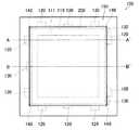
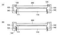
図1は、本発明のガラス基板保持手段の1実施形態を模式的に示した平面図である。図2(A)および図3(A)は図1中A−A´線に沿った断面図である。図2(B)および図3(B)は図1中B−B´線に沿った断面図である。これらの図では、本発明のガラス基板保持手段によって、ガラス基板をどのように保持するかという点を明確にするため、ガラス基板保持手段上にはガラス基板を示している。また、図2(A)、(B)はガラス基板の搬入時または離脱時の状態を示しており、図3(A)、(B)はガラス基板の保持時の状態を示している。
本発明のガラス基板保持手段は、静電チャック機構、および、機械的チャック機構を有しており、これらの機構を用いてガラス基板を保持する。The glass substrate holding means of the present invention will be described below with reference to the drawings.
FIG. 1 is a plan view schematically showing one embodiment of the glass substrate holding means of the present invention. 2A and 3A are cross-sectional views along the line AA ′ in FIG. 2B and 3B are cross-sectional views along the line BB ′ in FIG. In these drawings, a glass substrate is shown on the glass substrate holding means in order to clarify how the glass substrate is held by the glass substrate holding means of the present invention. 2A and 2B show the state when the glass substrate is carried in or removed, and FIGS. 3A and 3B show the state when the glass substrate is held.
The glass substrate holding means of the present invention has an electrostatic chuck mechanism and a mechanical chuck mechanism, and holds the glass substrate using these mechanisms.
本発明のガラス基板保持手段100では、静電チャック機構110によってガラス基板200の裏面を吸着保持する。
ここで、静電チャック機構110によるガラス基板200裏面の吸着保持のみに着目した場合、図2(A)、(B)に示すガラス基板200搬入時の状態から、図3(A)、(B)に示すガラス基板200の保持時の状態に移行するには、ガラス基板200裏面の四隅の端部付近を保持する支持ピン140を下降させて、ガラス基板200の裏面を静電チャック機構110の吸着保持部111の上面(吸着保持面)と接触させればよい。In the glass substrate holding means 100 of the present invention, the back surface of the
Here, when attention is paid only to the adsorption and holding of the back surface of the
上述したように、従来の静電チャックでは、ガラス基板の中心部、より具体的には、ガラス基板の裏面の中心部、を静電チャックの吸着保持面と接触させることによって、ガラス基板を吸着保持していた。
これに対して本発明のガラス基板保持手段100では、ガラス基板200の裏面中心部に存在する品質保証領域ではなく、該品質保証領域より外側の部位(以下、本明細書において、「裏面外周部」という。)を静電チャック110の吸着保持面(吸着保持部111の上面)と接触させることによってガラス基板を吸着保持する。このため、図示したガラス基板保持手段100の静電チャック110では、静電チャック110の上面のうち、外周部に凸部が設けられており、該凸部がガラス基板200の裏面外周部と接触する吸着保持部111をなす。
ここで、ガラス基板200の裏面の品質保証領域は、152.4mm角のガラス基板の場合、通常144mm角の領域であるので、静電チャック110上にガラス基板200を載置した際に、該144mm角の領域よりも外側の部位と接触するように、吸着保持部111をなす凸部を設ければよく、146mm角の領域よりも外側の部位と接触するように、吸着保持部111をなす凸部を設けることが好ましく、147mm角の領域よりも外側の部位と接触するように、吸着保持部111をなす凸部を設けることがより好ましく、148mm角の領域よりも外側の部位と接触するように、吸着保持部111をなす凸部を設けることがさらに好ましい。ガラス基板の裏面の品質保証領域が144mm角の領域とは異なる場合も、上記の同様の考え方で品質保証領域よりも外側の部位、好ましくは品質保証領域+2mm角の領域よりも外側の部位、より好ましくは品質保証領域+3mm角の領域よりも外側の部位、さらに好ましくは品質保証領域+4mm角の領域よりも外側の部位と接触するように、吸着保持部111をなす凸部を設ければよい。As described above, in the conventional electrostatic chuck, the glass substrate is adsorbed by bringing the central portion of the glass substrate, more specifically, the central portion of the back surface of the glass substrate into contact with the adsorption holding surface of the electrostatic chuck. Was holding.
On the other hand, in the glass substrate holding means 100 of the present invention, not the quality assurance region existing in the center of the back surface of the
Here, since the quality assurance area on the back surface of the
図示した静電チャック110のように、静電チャック110の上面のうち外周部に吸着保持部111をなす凸部が設ける方法としては、静電チャックの最表層をなす誘電体層にエンボス加工を施す方法がある。
図示した静電チャック110では、静電チャック110の上面の外周部に沿って枠組み状に、吸着保持部111をなす凸部が設けられているが、静電チャック上にガラス基板を載置した際に、静電チャックの上面に設けられた凸部がガラス基板の裏面外周部と接触する限り、吸着保持部をなす凸部の静電チャックにおける配置、および、個々の凸部の形状、寸法等は限定されない。たとえば、静電チャックの上面の外周部のうち、角部のみに吸着保持部をなす凸部が設けてもよく、その反対に角部以外の部分のみに吸着保持部をなす凸部を設けてもよい。なお、これらの態様の場合、静電チャックの上面に複数の凸部を設けることになるので、静電チャック上にガラス基板を載置した際に、ガラス基板を水平に保持できるよう、静電チャック上での凸部の配置に留意する必要がある。Like the
In the illustrated
静電チャック上にガラス基板を載置した際に、該静電チャックの上面に設けられた凸部のみをガラス基板の裏面と接触させるためには、該凸部の高さが5μm以上であることが好ましく、10μm以上であることがより好ましく、15μm以上であることがさらに好ましい。凸部の高さが5μm未満の場合、吸着保持力による凸部の変形によって、ガラス基板の裏面と、静電チャックの凸部以外の部分と、が接触するおそれがある。また、静電チャックの凸部以外の部分に存在する異物が、ガラス基板の裏面と接触してガラス基板の裏面に異物が転写されるおそれがある。
但し、凸部の高さが大きすぎると、静電チャックによる吸着保持力が低下するおそれがあるので、凸部の高さが100μm以下であることが好ましく、50μm以下であることがより好ましく、30μm以下であることがさらに好ましい。When the glass substrate is placed on the electrostatic chuck, the height of the convex portion is 5 μm or more so that only the convex portion provided on the upper surface of the electrostatic chuck is brought into contact with the back surface of the glass substrate. It is preferably 10 μm or more, more preferably 15 μm or more. When the height of the convex portion is less than 5 μm, the rear surface of the glass substrate and the portion other than the convex portion of the electrostatic chuck may come into contact with each other due to the deformation of the convex portion due to the suction holding force. Moreover, there is a possibility that foreign matters existing in portions other than the convex portion of the electrostatic chuck come into contact with the back surface of the glass substrate and the foreign matters are transferred to the back surface of the glass substrate.
However, if the height of the convex portion is too large, the suction holding force by the electrostatic chuck may be reduced. Therefore, the height of the convex portion is preferably 100 μm or less, more preferably 50 μm or less, More preferably, it is 30 μm or less.
本発明のガラス基板保持手段において 静電チャック機構の最表層をなす誘電体層は、非導通性であり、かつ保持力による変形が少なく剛性を持ち、耐摩耗性に優れた材料で作製されていることが好ましい。その一方で、吸着保持時にガラス基板に傷が生じるのを防止するために、ガラス基板よりも硬度が低い材料で作製されていることが好ましい。このような特性を満たす材料としては、アピカル(登録商標名、カネカ社製)のようなポリイミドフィルム、ニトフロン(登録商標名、日東電工社製)のようなフッ素樹脂フィルム等が挙げられる。これらの中でもアピカル(登録商標名、カネカ社製)のようなポリイミドフィルムが耐摩耗性に優れることから好ましい。
なお、誘電体層の硬度の目安については、後述する機械的チャック機構の押圧部に関する記載を参考にすればよい。In the glass substrate holding means of the present invention, the dielectric layer constituting the outermost layer of the electrostatic chuck mechanism is made of a material that is non-conductive, has little deformation due to holding force, has rigidity, and has excellent wear resistance. Preferably it is. On the other hand, it is preferable that the glass substrate is made of a material having a lower hardness than that of the glass substrate in order to prevent the glass substrate from being scratched during adsorption holding. Examples of the material satisfying such characteristics include a polyimide film such as Apical (registered trade name, manufactured by Kaneka Corporation), and a fluororesin film such as Nitoflon (registered trade name, manufactured by Nitto Denko Corporation). Among these, a polyimide film such as Apical (registered trademark, manufactured by Kaneka Corporation) is preferable because of its excellent wear resistance.
In addition, what is necessary is just to refer to the description regarding the press part of the mechanical chuck mechanism mentioned later about the standard of the hardness of a dielectric material layer.
本発明のガラス基板保持手段100において、機械的チャック機構は押圧部120を有している。該押圧部120でガラス基板200の成膜面の一部を押圧することにより、ガラス基板200を成膜面側および裏面側から挟持して保持することができる。ガラス基板200の保持時の状態は図3(A)に示されている。図3(A)において、ガラス基板200は、押圧部120と、静電チャック110の吸着保持部111をなす凸部と、によって、成膜面側および裏面側から挟持して保持されている。
ここで、押圧部120によるガラス基板200成膜面の押圧のみに着目した場合、図2(A)に示すガラス基板200搬入時の状態から、図3(A)に示すガラス基板の保持時の状態に移行するには、押圧部120が取り付けられたマスク150をガラス基板200に対して相対的に下降させればよい。なお、マスク150は、EUVマスクブランクスの製造時に実施される成膜プロセスの際に、膜材料がガラス基板200の側面側に廻りこむのを防止する目的で設けられている。In the glass substrate holding means 100 of the present invention, the mechanical chuck mechanism has a
Here, when attention is paid only to the pressing of the
本発明のガラス基板保持手段100では、ガラス基板200の成膜面の中心部に位置する品質保証領域より外側の部位(以下、本明細書において、「成膜面外周部」という。)を押圧部120で押圧する。上述したように、静電チャック110の吸着保持面(吸着保持部111の上面)はガラス基板200の裏面外周部と接触するので、ガラス基板200はその外周部(成膜面外周部および裏面外周部)において、成膜面側および裏面側から挟持して保持されることになる。よって、ガラス基板200の成膜面および裏面の中心部に位置する品質保証領域には、機械的チャック機構の押圧部120、および、静電チャック110の吸着保持面(吸着保持部111の上面)といった、ガラス基板保持手段100の構成要素が接触することがない。
これにより、保持によるガラス基板の品質保証領域(成膜面および裏面の品質保証領域)への傷の発生や異物の付着を抑制することができる。
ここで、ガラス基板200の成膜面の品質保証領域は、152.4mm角のガラス基板の場合、通常中心部の148mm角の領域であるので、機械的チャック機構の押圧部120は、該148mm角の領域よりも外側の部位を押圧するように設けられていればよく、150mm角の領域よりも外側の部位を押圧するように設けられていることが好ましい。ガラス基板の成膜面の品質保証領域が148mm角の領域とは異なる場合も、上記の同様の考え方で品質保証領域+2mm角の領域よりも外側の部位、好ましくは品質保証領域+2mm角の領域よりも外側の部位と接触するように、吸着保持部111をなす凸部を設ければよい。
また、ガラス基板の成膜面側の外周部に面取り部が設けられている場合は、該面取り部を押圧するように機械的チャック機構の押圧部が設けられていることがさらに好ましい。In the glass substrate holding means 100 of the present invention, a portion outside the quality assurance region located in the center of the film formation surface of the glass substrate 200 (hereinafter referred to as “film formation surface outer peripheral portion”) is pressed. Press with
Thereby, generation | occurrence | production of the damage | wound and adhesion of a foreign material to the quality assurance area | region (the quality assurance area | region of a film-forming surface and a back surface) of the glass substrate by holding | maintenance can be suppressed.
Here, in the case of a 152.4 mm square glass substrate, the quality assurance area of the film formation surface of the
Moreover, when the chamfering part is provided in the outer peripheral part by the side of the film-forming surface of a glass substrate, it is still more preferable that the press part of a mechanical chuck mechanism is provided so that this chamfering part may be pressed.
図2(A)および図3(A)において、押圧部120の押圧面は、該押圧部120によって押圧されるガラス基板200の成膜面に対して傾斜している。
図示した態様のように、本発明のガラス基板保持手段100において、押圧部120の押圧面は、該押圧部120によって押圧されるガラス基板200の成膜面に対して傾斜していることが好ましい。その理由は、成膜面外周部のうち、より外側の部位を押圧することが可能となるからである。図3(A)では、押圧部120によって、ガラス基板200の成膜面と側面との境界をなす辺を押圧している。
成膜面外周部のうち、より外側の部位を押圧することは、保持によるガラス基板の品質保証領域(成膜面の品質保証領域)への傷の発生や異物の付着を抑制するうえで好ましい。
また、押圧部120の押圧面がガラス基板200の成膜面に対して傾斜していることは以下の点でも好ましい。
特許文献2に記載のガラス基板押圧手段4(以下、特許文献2に関する記載における符号は同文献での記載での符号の通りである。)は、基板1を押圧する際に、該ガラス基板押圧手段4のクランプ部材41先端の爪部41aが基板1の主表面1aの端部と当接するものであるが、当接時において、該爪部41aの当接面と、主表面1aと、が平行な状態、つまり、両者が面接触した状態となる。このような構成の場合、EUVマスクブランクの製造時に実施される成膜手順の際に、基板1の主表面1a(本願における成膜面)および爪部41aの両方に膜材料が連続して付着する部分が生じる。ガラス基板押圧手段4による押圧を解除する際、このような部分の膜が剥離し、異物を発生させるおそれがある。
これに対し、図2(A)および図3(A)に示す態様のように、押圧部120の押圧面が、ガラス基板200の成膜面に対して傾斜していれば、EUVマスクブランクの製造時に実施される成膜手順の際に、ガラス基板200の成膜面および押圧部120の両方に膜材料が連続して付着する部分が生じにくくなるので、押圧部120による押圧を解除する際に、膜が剥離し、異物を発生させるおそれが抑制される。2A and 3A, the pressing surface of the
Like the aspect shown in figure, in the glass substrate holding means 100 of this invention, it is preferable that the press surface of the
It is preferable to press the outer part of the outer peripheral portion of the film formation surface in order to suppress the occurrence of scratches and the adhesion of foreign substances to the quality assurance region (quality assurance region of the film formation surface) of the glass substrate due to the holding. .
Moreover, it is preferable also in the following points that the pressing surface of the
When the substrate 1 is pressed, the glass substrate pressing means 4 described in Patent Document 2 (hereinafter, the reference numerals relating to the Patent Document 2 are the same as those described in the same document). The claw portion 41a at the tip of the clamp member 41 of the means 4 is in contact with the end portion of the main surface 1a of the substrate 1. At the time of contact, the contact surface of the claw portion 41a and the main surface 1a are A parallel state, that is, a state where both are in surface contact. In the case of such a configuration, the film material continuously adheres to both the main surface 1a (deposition surface in the present application) and the claw portion 41a of the substrate 1 during the film formation procedure performed when manufacturing the EUV mask blank. The part to be generated occurs. When the pressing by the glass substrate pressing means 4 is released, such a portion of the film may be peeled off and foreign matter may be generated.
On the other hand, if the pressing surface of the
本発明のガラス基板保持手段100において、押圧部120の押圧面と、ガラス基板200の成膜面と、のなす角度が5〜70度であることが好ましい。両者のなす角度が5度未満だと、また、特許文献2に記載のガラス基板押圧手段の場合のように、両者が平行な状態に近づくため、ガラス基板200の成膜面および押圧部120の両方に膜材料が連続して付着する部分が生じやすくなり、押圧部120による押圧を解除する際に、膜が剥離し、異物を発生させるおそれがある。
また、成膜面外周部のうち、より内側の部位を押圧することになるため、保持によるガラス基板の品質保証領域(成膜面の品質保証領域)への傷の発生や異物の付着を抑制するうえで好ましくない。
一方、両者のなす角度が70度超だと、押圧部がガラス基板の側面に沿った形に変形してしまい、ガラス基板を押圧することが困難となるおそれがある。
両者のなす角度は10〜65度であることが好ましく、20〜60度であることがより好ましく、30〜55度であることがさらに好ましい。In the glass substrate holding means 100 of the present invention, the angle formed by the pressing surface of the
In addition, since the inner part of the outer peripheral part of the film formation surface is pressed, the generation of scratches and adhesion of foreign matter to the glass substrate quality assurance region (deposition surface quality assurance region) due to holding is suppressed. This is not preferable.
On the other hand, if the angle formed by both is more than 70 degrees, the pressing portion is deformed into a shape along the side surface of the glass substrate, and it may be difficult to press the glass substrate.
The angle formed by the two is preferably 10 to 65 degrees, more preferably 20 to 60 degrees, and still more preferably 30 to 55 degrees.
図2(A)および図3(A)において、機械的チャック機構の押圧部120の押圧面は平面をなしているが、機械的チャック機構の押圧部の押圧面は湾曲面であってもよい。この場合、押圧部をなす湾曲面のうち、ガラス基板の成膜面と当接する位置における接線と、ガラス基板の成膜面と、がなす角度が上記した押圧面と、成膜面と、のなす角度に該当する。 2A and 3A, the pressing surface of the
図1において、矩形をしたガラス基板200の成膜面の外縁をなす4辺に対して、機械的チャック機構の押圧部120が各々2つずつ設けられている。別の言い方をすると、ガラス基板200の成膜面の外縁をなす4辺には、それぞれ外縁をなす辺を含む位置、若しくは、外縁をなす辺に近接する位置に、機械的チャック機構(の押圧部120)による被押圧部が2個所ずつ存在する。 In FIG. 1, two
外縁をなす辺を含む位置に機械的チャック機構による被押圧部が存在する場合とは、図3(A)に示す態様のように、ガラス基板200の成膜面の外縁をなす辺上に機械的チャック機構(の押圧部120)による被押圧部が存在する場合を指す。但し、押圧部120の形状によっては、外縁をなす辺だけではなく該辺よりも成膜面の内側部分も押圧する場合もあるため、外縁をなす辺を含む位置に機械的チャック機構による被押圧部が存在すると記載する。
一方、外縁をなす辺に近接する位置に機械的チャック機構による被押圧部が存在する場合とは、ガラス基板200の成膜面の外縁よりもなす辺上には機械的チャック機構(の押圧部120)による被押圧部が存在せず、外縁をなす辺よりも成膜面の内側部分にのみ機械的チャック機構による被押圧部が存在する場合を指す。
以下、本明細書において、成膜面の外縁をなす辺を含む位置に機械的チャック機構による被押圧部が存在する場合と、外縁をなす辺に近接する位置に被押圧部が存在する場合を総称して、成膜面の外縁をなす辺に機械的チャック機構による被押圧部が存在するという。The case where the pressed portion by the mechanical chuck mechanism is present at a position including the edge forming the outer edge means that the machine is formed on the edge forming the outer edge of the film formation surface of the
On the other hand, the case where the pressed portion by the mechanical chuck mechanism is present at a position close to the side forming the outer edge means that the mechanical chuck mechanism (the pressing portion of the mechanical chuck mechanism (on the side formed by the outer edge of the film forming surface of the glass substrate 200) is located. 120) indicates that the pressed part by the mechanical chuck mechanism exists only in the inner part of the film formation surface rather than the side forming the outer edge.
Hereinafter, in the present specification, a case where the pressed portion by the mechanical chuck mechanism exists at a position including the side forming the outer edge of the film forming surface, and a case where the pressed portion exists at a position close to the side forming the outer edge. Collectively, it is said that there is a pressed portion by a mechanical chuck mechanism on the side that forms the outer edge of the film formation surface.
図1では、ガラス基板200の成膜面の外縁をなす4辺に、機械的チャック機構(の押圧部120)による被押圧部がそれぞれ2個所ずつ存在するが、外縁をなす辺に対する被押圧部の数はこれに限定されず、各辺に被押圧部がそれぞれ1個所ずつ存在してもよく、それぞれ3個所以上存在してもよい。また、外縁をなす辺ごとに被押圧部の数が異なっていてもよい。 In FIG. 1, there are two pressed parts by the mechanical chuck mechanism (pressing
また、図1では、ガラス基板200の成膜面の外縁をなす4辺全てに、機械的チャック機構(の押圧部120)による被押圧部が存在するが、これに限定されない。
本発明のガラス基板保持手段100では、ガラス基板200の成膜面の外縁をなす4辺のうち、少なくとも対向する2辺(例えば、図1中、上側の辺と下側の辺)に機械的チャック機構による被押圧部が存在すれば、ガラス基板200を水平に保持することが可能である。
本発明のガラス基板保持手段では、ガラス基板の成膜面の外縁をなす4辺のうち、3辺に機械的チャック機構による被押圧部が存在することが好ましく、4辺全てに機械的チャック機構による被押圧部が存在することがより好ましい。Moreover, in FIG. 1, although the to-be-pressed part by the mechanical chuck | zipper mechanism (pressing part 120) exists in all four sides which make the outer edge of the film-forming surface of the
In the glass substrate holding means 100 of the present invention, at least two sides facing each other (for example, the upper side and the lower side in FIG. 1) among the four sides forming the outer edge of the film formation surface of the
In the glass substrate holding means of the present invention, it is preferable that the pressed part by the mechanical chuck mechanism is present on three sides among the four sides forming the outer edge of the film formation surface of the glass substrate. More preferably, there is a pressed part.
本発明のガラス基板保持手段において、機械的チャック機構の押圧部は、ガラス基板の押圧時に破損することがないよう、十分な硬度を有している必要がある。
しかしながら、押圧部が、押圧されるガラス基板よりも高い硬度を有していると、押圧時にガラス基板に傷が生じるおそれがある。
このため、押圧部が、押圧されるガラス基板よりも硬度が低い材料で作成されていることが好ましい。
押圧部の硬度の目安としては、ビッカース硬さ(HV)が650未満であることが好ましく、100以下であることがより好ましく、30以下であることがさらに好ましい。In the glass substrate holding means of the present invention, the pressing portion of the mechanical chuck mechanism needs to have sufficient hardness so as not to be damaged when the glass substrate is pressed.
However, if the pressing portion has a higher hardness than the glass substrate to be pressed, there is a risk that the glass substrate will be damaged during pressing.
For this reason, it is preferable that the pressing part is made of a material whose hardness is lower than that of the glass substrate to be pressed.
As a measure of the hardness of the pressing part, the Vickers hardness (HV) is preferably less than 650, more preferably 100 or less, and even more preferably 30 or less.
また、本発明のガラス基板保持手段において、機械的チャック機構の押圧部は、EUVマスクブランクスの製造時に実施される成膜プロセス下に置かれるため、成膜容器内の真空雰囲気下において、ガス成分を放出するものであってはならない。さらに、成膜装置では基板などが熱を持つ場合があるため、機械的チャック機構の押圧部は、少なくとも約150℃程度まで化学的・物理的に耐熱性を有していることが求められる。 Further, in the glass substrate holding means of the present invention, the pressing portion of the mechanical chuck mechanism is placed under a film forming process performed at the time of manufacturing EUV mask blanks. Must not release. Further, since the substrate or the like may have heat in the film forming apparatus, the pressing portion of the mechanical chuck mechanism is required to have chemical and physical heat resistance up to at least about 150 ° C.
以上の点を満たすことが必要であることから、機械的チャック機構の押圧部の構成材料としては、パーフロロエラストマー、フッ素ゴム、シリコーンゴム等のエラストマー材料や、ポリエーテルエーテルケトン(PEEK)、ポリイミド、ポリベンゾイミダゾール(PBI)樹脂、フッ素樹脂等を用いることができる。これらの中でも、パーフロロエラストマー、フッ素ゴムが好ましく、パーフロロエラストマーがより好ましい。 Since it is necessary to satisfy the above points, as a constituent material of the pressing portion of the mechanical chuck mechanism, elastomer materials such as perfluoroelastomer, fluororubber, and silicone rubber, polyetheretherketone (PEEK), polyimide Polybenzimidazole (PBI) resin, fluororesin, and the like can be used. Among these, perfluoroelastomer and fluororubber are preferable, and perfluoroelastomer is more preferable.
本発明のガラス基板保持手段は、EUVマスクブランクスの製造時において、位置ずれや脱離が起こすことなくガラス基板を保持することが求められる。
本発明のガラス基板保持手段は、静電チャック機構によるガラス基板の吸着保持力と、機械的チャック機構によるガラス基板の保持力と、の和が、200kgf以上と高いため、EUVマスクブランクスの製造時において、位置ずれや脱離が起こすことなくガラス基板を保持することができる。
本発明のガラス基板保持手段において、静電チャック機構によるガラス基板の吸着保持力と、機械的チャック機構によるガラス基板の保持力と、の和が、240kgf以上であることが好ましく、280kgf以上であることがより好ましい。The glass substrate holding means of the present invention is required to hold the glass substrate without causing displacement or detachment during the production of EUV mask blanks.
The glass substrate holding means of the present invention has a high sum of 200 kgf or more of the glass substrate suction holding force by the electrostatic chuck mechanism and the glass substrate holding force by the mechanical chuck mechanism. In this case, it is possible to hold the glass substrate without causing displacement or detachment.
In the glass substrate holding means of the present invention, the sum of the glass substrate suction holding force by the electrostatic chuck mechanism and the glass substrate holding force by the mechanical chuck mechanism is preferably 240 kgf or more, and preferably 280 kgf or more. It is more preferable.
上述したように、ガラス基板の裏面外周部を静電チャックで吸着保持する場合、ガラス基板の被吸着保持部の表面積が小さくなるため、ガラス基板を保持するのに十分な大きさの吸着保持力を発揮させた場合、被吸着保持部への単位面積当たりの圧力が高くなり、該被吸着保持部での傷の発生やそれによる異物の発生が問題となるおそれがある。また、該被吸着保持部に対して局所的に静電引力(クーロン力や誘電体引力)が加わるため、残留電荷や漏洩電場によって該被吸着保持部に多量の異物を引き付けられるおそれがある。
被吸着保持部は裏面の外縁部に存在するため、傷や異物の発生による影響は裏面の品質保証領域で同様の問題が生じた場合に比べると小さいが、被吸着保持部で発生した異物や、該被吸着保持部に引きつけられた異物の一部が裏面の品質保証領域に転写されるおそれがある。
ガラス基板の成膜面外周部を機械的チャック機構によって保持する場合も同様であり、ガラス基板を保持するのに十分な大きさの保持力を発揮させた場合、ガラス基板の被保持部位への単位面積当たりの圧力が高くなり、ガラス基板の被保持部での傷の発生やそれによる異物の発生が問題となるおそれがある。
なお、ガラス基板の成膜面外周部および裏面外周部における欠点に関する要求については、成膜面および裏面の品質保証領域における欠点に関する要求とともに後述する。As described above, when the outer peripheral portion of the back surface of the glass substrate is attracted and held by the electrostatic chuck, the surface area of the attracted and held portion of the glass substrate is reduced, so that the suction holding force is large enough to hold the glass substrate. When the pressure is exerted, the pressure per unit area to the suction holding unit becomes high, and there is a possibility that the generation of scratches and the generation of foreign matters due to the suction holding unit may occur. In addition, since electrostatic attraction (Coulomb force or dielectric attraction) is locally applied to the attracted / held portion, a large amount of foreign matter may be attracted to the attracted / held portion due to residual charges or leakage electric field.
Since the suction holding part is located on the outer edge of the back surface, the impact of scratches and foreign matter is small compared to the case where the same problem occurs in the quality assurance area on the back side. There is a risk that a part of the foreign matter attracted to the sucked and held portion may be transferred to the quality assurance area on the back surface.
The same applies to the case where the outer peripheral portion of the film formation surface of the glass substrate is held by a mechanical chuck mechanism. When a holding force large enough to hold the glass substrate is exhibited, The pressure per unit area becomes high, and there is a possibility that the generation of scratches and the generation of foreign matters due to the scratch on the held portion of the glass substrate may occur.
In addition, the request | requirement regarding the fault in the film-forming surface outer periphery of a glass substrate and a back surface outer peripheral part is mentioned later with the request regarding the defect in the quality assurance area | region of a film-forming surface and a back surface.
本発明のガラス基板保持手段では、静電チャック機構による吸着保持と、機械的チャック機構による保持を併用することにより、ガラス基板の保持部への単位面積当たりの圧力(静電チャック機構による吸着保持部への単位面積当たりの圧力、および、機械的チャック機構による吸着保持部への単位面積当たりの圧力)を過度に増加することなしに、ガラス基板を保持するのに十分な大きさの保持力を発揮することができる。これにより、EUVマスクブランクの製造時において、ガラス基板の成膜面外周部および裏面外周部への傷の発生や異物の付着を抑制しつつ、ガラス基板の位置ずれや脱離が防止できる。 In the glass substrate holding means of the present invention, the pressure per unit area on the holding portion of the glass substrate (adsorption holding by the electrostatic chuck mechanism) is achieved by using both the adsorption holding by the electrostatic chuck mechanism and the holding by the mechanical chuck mechanism. Holding force large enough to hold the glass substrate without excessively increasing the pressure per unit area on the part and the pressure per unit area on the suction holding part by the mechanical chuck mechanism) Can be demonstrated. Thereby, at the time of manufacture of an EUV mask blank, the position shift | offset | difference and detachment | desorption of a glass substrate can be prevented, suppressing the generation | occurrence | production of the damage | wound and the adhesion of a foreign material to the film-forming surface outer periphery and back surface outer periphery.
本発明のガラス基板保持手段では、静電チャック機構によるガラス基板の吸着保持力と、機械的チャック機構によるガラス基板の保持力と、の和が、200kgf以上であればよく、上限は特に限定されないが、500kgf以下が基板に無理な力をかけずに保持できる目安となる。基板に無理な力をかけると基板が変形する場合もあるので好ましくない。
それぞれのチャック機構による保持力の内訳は特に限定されないが、機械的チャック機構によるガラス基板の単位面積当たりの押圧力が大きすぎると、ガラス基板の被押圧部での傷の発生やそれによる異物の発生が問題となるおそれがある。
このため、機械的チャック機構によるガラス基板の単位面積当たりの押圧力は、25kgf/mm2以下であることが求められる。
本発明のガラス基板保持手段において、機械的チャック機構によるガラス基板の単位面積当たりの押圧力は、10kgf/mm2以下であることが好ましく、5kgf/mm2以下であることがより好ましく、1kgf/mm2以下であることがさらに好ましい。In the glass substrate holding means of the present invention, the sum of the adsorption holding force of the glass substrate by the electrostatic chuck mechanism and the holding force of the glass substrate by the mechanical chuck mechanism may be 200 kgf or more, and the upper limit is not particularly limited. However, 500 kgf or less is an indication that the substrate can be held without applying an excessive force. Unfavorably cases be the substrate and the substrate thatPlacing an excessive force to deform.
The breakdown of the holding force by each chuck mechanism is not particularly limited. However, if the pressing force per unit area of the glass substrate by the mechanical chuck mechanism is too large, scratches on the pressed portion of the glass substrate and the occurrence of foreign substances due to it Occurrence may be a problem.
For this reason, the pressing force per unit area of the glass substrate by the mechanical chuck mechanism is required to be 25 kgf /mm2 or less.
In the glass substrate holding means of the present invention, the pressing force per unit area of the glass substrate by the mechanical chuck mechanism is preferably 10 kgf /mm2 or less, more preferably 5 kgf /mm2 or less, and 1 kgf /mm2. even more preferablymm2 or less.
本発明のガラス基板保持手段において、静電チャック機構によるガラス基板の吸着保持力が30kgf以上であることが好ましく、50kgf以上であることがより好ましく、100kgf以上であることがさらに好ましく、150kgf以上であることがさらに好ましい。また、静電チャック機構によるガラス基板の吸着保持力が250kgf以下であることが好ましく、200kgf以下であることがより好ましい。
本発明のガラス基板保持手段において、機械的チャック機構によるガラス基板の保持力が250kgf以下であることが好ましく、200kgf以下であることがより好ましく、150kgf以下であることがさらに好ましい。また、機械的チャック機構によるガラス基板の保持力が、30kgf以上であることが好ましく、50kgf以上であることがより好ましい。In the glass substrate holding means of the present invention, the adsorption holding force of the glass substrate by the electrostatic chuck mechanism is preferably 30 kgf or more, more preferably 50 kgf or more, further preferably 100 kgf or more, more preferably 150 kgf or more. More preferably it is. Moreover, it is preferable that the adsorption holding force of the glass substrate by an electrostatic chuck mechanism is 250 kgf or less, and it is more preferable that it is 200 kgf or less.
In the glass substrate holding means of the present invention, the holding force of the glass substrate by the mechanical chuck mechanism is preferably 250 kgf or less, more preferably 200 kgf or less, and further preferably 150 kgf or less. Further, the holding force of the glass substrate by the mechanical chuck mechanism is preferably 30 kgf or more, and more preferably 50 kgf or more.
図1〜図3に示すガラス基板保持手段100を使用する際には、ロボットアーム等の搬送手段(図示しない)を用いてガラス基板200を静電チャック機構110の上方の所定の位置(具体的には、ガラス基板200の四隅の端部付近が支持ピン140の上方となる位置)まで搬送し、ガラス基板200裏面の四隅の端部付近を支持ピン140で保持する。以下、本明細書において、搬送手段を用いてガラス基板を静電チャック機構の上方の所定の位置まで搬送し、ガラス基板裏面の四隅の端部付近を支持ピンで保持する手順を、ガラス基板保持手段にガラス基板を載置する手順と言う。
次に、搬送手段によるガラス基板200の保持を解き、搬送手段をガラス基板保持手段100の外部に移動させる。搬送手段が後述するロボットアーム300の場合、該ロボットアーム300を後退させて、ガラス基板保持手段100の外部に移動させる。次に、支持ピン140を下降させて、ガラス基板200の裏面を静電チャック機構110の吸着保持面(吸着保持部111の上面)と接触させることで、静電チャック機構110によってガラス基板200を吸着保持する。その後、押圧部120が取り付けられたマスク150をガラス基板200に対して相対的に下降させることで、押圧部120と、静電チャック110の吸着保持面111と、によって、ガラス基板200を挟持して保持する。When the glass substrate holding means 100 shown in FIGS. 1 to 3 is used, the
Next, the holding of the
上記の過程において、ガラス基板保持手段にガラス基板を載置する際に、ガラス基板保持手段とガラス基板との位置関係が適切な状態となるように位置決めすること、具体的には両者が常に水平となる位置関係を保つように位置決めすることが重要である。以下、本明細書において、ガラス基板保持手段とガラス基板との位置関係が適切であると言った場合、両者が常に水平となる位置関係に保たれていることを指す。
ガラス基板保持手段とガラス基板との位置関係が適切でない場合、EUVマスクブランクの製造時に実施される成膜手順の際に、ガラス基板の成膜面外周部に膜材料が付着するおそれがある。ガラス基板の成膜面外周部への膜材料の付着は、異物の発生源となる等の理由から好ましくない。
また、ガラス基板保持手段100とガラス基板200との位置関係が適切でないと、ガラス基板200裏面の四隅のいずれかが支持ピン140の上方に位置していない状態となり、搬送手段によるガラス基板200の保持を解いた際に、ガラス基板200が支持ピン140から落下したり、ガラス基板200が傾いた状態で静電チャック110の吸着保持面111と接触することで、ガラス基板200の被吸着保持部に傷が発生するおそれがある。
このため、本発明のガラス基板保持手段は、ガラス基板保持手段にガラス基板を載置する際に、ガラス基板保持手段とガラス基板との位置関係が適切な状態となるように位置決めする位置決め手段を有していることが好ましい。In the above process, when placing the glass substrate on the glass substrate holding means, positioning so that the positional relationship between the glass substrate holding means and the glass substrate is in an appropriate state, specifically, both are always horizontal. It is important to perform positioning so as to maintain the positional relationship. Hereinafter, in this specification, when it is said that the positional relationship between the glass substrate holding means and the glass substrate is appropriate, it means that both are always maintained in a horizontal positional relationship.
When the positional relationship between the glass substrate holding means and the glass substrate is not appropriate, there is a possibility that the film material adheres to the outer peripheral portion of the film forming surface of the glass substrate during the film forming procedure performed when manufacturing the EUV mask blank. Adhesion of the film material to the outer peripheral portion of the film formation surface of the glass substrate is not preferable because it becomes a source of foreign matter.
Further, if the positional relationship between the glass substrate holding means 100 and the
For this reason, the glass substrate holding means of the present invention includes positioning means for positioning so that the positional relationship between the glass substrate holding means and the glass substrate is in an appropriate state when the glass substrate is placed on the glass substrate holding means. It is preferable to have.
図示したガラス基板保持手段100は、位置決め手段130を有している。但し、上述した点から明らかなように、本発明のガラス基板保持手段において、位置決め手段は必須の構成要件ではない。
図2(B)に示すように、位置決め手段130はガラス基板200の側面および底面(裏面)に対して傾斜したガイド面を有しており、ガラス基板保持手段100にガラス基板200を載置する際に、該ガイド面がガラス基板200の側面と底面(裏面)との境界をなす辺(以下、本明細書において、「ガラス基板の底辺」という。)と当接する。ここで、位置決め手段130のガイド面は、ガラス基板200の側面および底面(裏面)に対して傾斜しているので、位置決め手段130のガイド面にガラス基板200の底辺を当接させた際、ガラス基板200は自重によって下方に移動する。ここで、位置決め手段130をガラス基板保持手段100の静電チャック機構110に対して適切な位置に配置しておけば、ガラス基板200は自重によって下方に移動することで、ガラス基板保持手段100とガラス基板200との位置関係、より具体的には、ガラス基板保持手段100の静電チャック機構110とガラス基板200との位置関係が適切な状態となるように位置決めすることができる。The illustrated glass substrate holding means 100 has positioning means 130. However, as is apparent from the above points, in the glass substrate holding means of the present invention, the positioning means is not an essential component.
As shown in FIG. 2B, the positioning means 130 has a guide surface that is inclined with respect to the side surface and the bottom surface (back surface) of the
図4(a)〜(e)は、ガラス基板保持手段100にガラス基板200を載置する際に、位置決め手段130によって、ガラス基板保持手段100とガラス基板200との位置関係が適切な状態となるように位置決めする手順を示した図であり、図1中B−B´線に沿った断面図に相当する。但し、理解を容易にするため、ガラス基板保持手段100の構成要素のうち、マスク部150と該マスク部150に取り付けられた機械的チャック機構の押圧部120は省略されている。 4A to 4E show a state in which the positional relationship between the glass substrate holding means 100 and the
図4(a)〜(e)では、ガラス基板200の搬送手段として、ロボットアーム300を使用する。図4(a)において、ガラス基板200はガラス基板保持手段100の外部でロボットアーム300に載せられている。この状態から、ロボットアーム300を前進させて、図4(b)に示すように、ガラス基板200をガラス基板保持手段100の静電チャック機構110の上方に移動させる。ここで、ロボットアーム300を図中左方向に移動させることをロボットアーム300を前進させると言い、ロボットアーム300を図中右方向に移動させることをロボットアーム300を後退させると言う。また、ロボットアーム300を図中上方向に移動させることをロボットアーム300を上昇させると言い、ロボットアーム300を図中下方向に移動させることをロボットアーム300を下降させると言う。 4A to 4E, a
次に、ロボットアーム300を下降させて、図4(c)に示すように、ガラス基板200の底辺を位置決め手段130のガイド面に当接させる。図4(c)では図中左側にのみ位置決め手段130が示されているが、図1に示すように、ガラス基板200の4辺全てに対して、位置決め手段130が存在する。ここで、図中、右側のみ位置決め手段130の位置が異なるのは、図中右側からロボットアーム300が進入することを想定しているためである。
その後、ロボットアーム300をさらに下降させて、ガラス基板200裏面の四隅の端部付近を支持ピン140で保持し、ロボットアーム300によるガラス基板200の保持を解く。
ここで、ガラス基板200の底辺を位置決め手段130のガイド面に当接した状態からロボットアーム300を下降させると、ガラス基板200が自重によって下方に移動することによって、ガラス基板保持手段100の静電チャック機構110とガラス基板200との位置関係が適切な状態となるように位置決めされ、その後にガラス基板200裏面の四隅の端部付近が支持ピン140で保持される。この手順を達成するため、位置決め手段130のガイド面のガラス基板200の底辺と当接する部位が、ガラス基板200の支持ピン140の上端よりも上方に位置する必要がある。Next, the
Thereafter, the
Here, when the
次に、図4(d)に示すように、ロボットアーム300をガラス基板保持手段100の外部に後退させる。図2(B)はこの段階に相当する。
次に、支持ピン140と位置決め手段130(実際には位置決め手段130が取り付けられたマスク150)を下降させて、図4(e)に示すように、ガラス基板200の裏面を静電チャック機構110の吸着保持面(吸着保持部111の上面)と接触させることによって、ガラス基板200が静電チャック機構110で吸着保持される。Next, as shown in FIG. 4D, the
Next, the support pins 140 and the positioning means 130 (actually the
本発明のガラス基板保持手段において、位置決め手段130のガイド面と、ガラス基板200の底面(裏面)と、がなす角度は5度以上90度未満である。
両者がなす角度が5度未満の場合、ガラス基板200の底辺を位置決め手段130のガイド面に当接させた際にガラス基板200の保持が不十分となり、ガラス基板200が自重によって下方に移動する際にガラス基板200が傾くおそれがある。自重によって下方に移動する際にガラス基板200が傾くと、静電チャック機構110とガラス基板200との位置関係が適切な状態となるように位置決めできなくなるおそれがあるうえ、支持ピン140と接した際にガラス基板200が水平方向に移動することによって、ガラス基板200の裏面に傷が発生するおそれがある。
両者がなす角度は20〜70度であることが好ましく、30〜60度であることがより好ましい。
図示した態様において、支持部材130のガイド面は平面をなしているが、支持部材130のガイド面は湾曲面であってもよい。この場合、ガイド面をなす湾曲面のうち、ガラス基板の底辺と当接する位置における接線と、ガラス基板200の底面(裏面)と、がなす角度が、上記した位置決め手段のガイド面と、ガラス基板の底面(裏面)と、がなす角度に該当する。In the glass substrate holding means of the present invention, the angle formed by the guide surface of the positioning means 130 and the bottom surface (back surface) of the
When the angle formed by the two is less than 5 degrees, the
The angle formed by the two is preferably 20 to 70 degrees, and more preferably 30 to 60 degrees.
In the illustrated embodiment, the guide surface of the
図1では、ガラス基板200の4辺全てに対して支持部材130が設けられているが、これに限定されない。
本発明のガラス基板保持手段では、ガラス基板の4つの底辺のうち、少なくとも直交する2辺(例えば、図1中、上側の辺と左側の辺)に対して支持部材が設ければ、ガラス基板保持手段100の静電チャック機構110とガラス基板200との位置関係が適切な状態となるように位置決めすることができる。
本発明のガラス基板保持手段では、ガラス基板の4つの底辺のうち、少なくとも直交する2辺に対して1つずつ位置決め手段を設ければ、ガラス基板保持手段の静電チャック機構とガラス基板との位置関係が適切な状態となるように位置決めすることができる。
本発明のガラス基板保持手段では、ガラス基板の4つの底辺のうち、3辺に対して支持部材を設けることが好ましく、4辺全てに対して支持部材を設けることがより好ましい。
また、図1に示すガラス基板保持手段100では、ガラス基板200の4つの底辺のうち、3辺については1つの位置決め手段130、図中右側の辺については2つの位置決め手段130が設けられているが、各底辺に対する位置決め手段の数はこれに限定されず、各辺に対して2つ以上の位置決め手段を設けてもよく、各辺に対して位置決め手段を1つずつ設けたのでもよい。In FIG. 1, the
In the glass substrate holding means of the present invention, if the supporting member is provided on at least two orthogonal sides (for example, the upper side and the left side in FIG. 1) among the four bottom sides of the glass substrate, the glass substrate Positioning can be performed so that the positional relationship between the
In the glass substrate holding means of the present invention, if one positioning means is provided for each of at least two orthogonal sides among the four bottom sides of the glass substrate, the electrostatic chuck mechanism of the glass substrate holding means and the glass substrate Positioning can be performed so that the positional relationship is in an appropriate state.
In the glass substrate holding means of the present invention, it is preferable to provide support members for three sides of the four bottom sides of the glass substrate, and it is more preferable to provide support members for all four sides.
Further, in the glass substrate holding means 100 shown in FIG. 1, among the four bottom sides of the
本発明のガラス基板保持手段において、ガラス基板の4つの底辺のうち、直交する2辺に対して1つずつ位置決め手段が設ける場合、位置決め手段が設けられた底辺の長さをL(mm)とするとき、該底辺のうち、位置決め手段のガイド面と当接する部分の端部と、該底辺の端部と、の距離が0.1L以上となる位置に位置決め手段を設けることが好ましい。
直交する2つの底辺に対して1つずつ位置決め手段が設けた場合に、位置決め手段のガイド面と当接する部分の端部と、該底辺の端部と、の距離が0.1L未満だと、ガラス基板200の底辺を位置決め手段130のガイド面に当接させた際にガラス基板200の保持が不十分となり、ガラス基板200が自重によって下方に移動する際にガラス基板200が傾くおそれがある。自重によって下方に移動する際にガラス基板200が傾くと、静電チャック機構110とガラス基板200との位置関係が適切な状態となるように位置決めできなくなるおそれがあるうえ、支持ピン140と接した際にガラス基板200が水平方向に移動することによって、ガラス基板200の裏面に傷が発生するおそれがある。
直交する2つの底辺に対して1つずつ位置決め手段が設ける場合に、支持部材のガイド面と当接する部分の端部と、該底辺の端部と、の距離が0.2L以上であることが好ましく、0.3L以上であることがより好ましい。
ガラス基板の4つの底辺のうち、直交する2辺に対して位置決め手段が設ける場合であっても、各底辺に対して2つ以上の位置決め手段を設ければ、上記の問題が起こらないため、支持部材のガイド面と当接する部分の端部と、該底辺の端部と、の距離がこれに限定されない。In the glass substrate holding means of the present invention, when the positioning means is provided one by one with respect to two orthogonal sides among the four bottom edges of the glass substrate, the length of the bottom edge on which the positioning means is provided is L (mm). In this case, it is preferable that the positioning means is provided at a position where the distance between the end of the portion contacting the guide surface of the positioning means and the end of the bottom becomes 0.1 L or more.
When positioning means are provided one by one for two orthogonal bottom sides, if the distance between the end of the portion that contacts the guide surface of the positioning means and the end of the bottom is less than 0.1 L, When the bottom of the
When positioning means are provided for each of two orthogonal bottom sides, the distance between the end portion of the support member in contact with the guide surface and the end portion of the bottom side is 0.2 L or more. Preferably, it is 0.3 L or more.
Even if the positioning means is provided for two sides orthogonal to each other among the four bottom sides of the glass substrate, if two or more positioning means are provided for each bottom side, the above problem does not occur. The distance between the end portion of the support member that contacts the guide surface and the bottom end portion is not limited to this.
本発明のガラス基板保持手段において、位置決め手段は、ガラス基板の底辺との当接時に破損することがないよう、十分な硬度を有している必要がある。
しかしながら、位置決め手段がガラス基板よりも高い硬度を有していると、当接時にガラス基板に傷が生じるおそれがある。
このため、位置決め手段はガラス基板よりも硬度が低い材料で作成されていることが好ましい。
位置決め手段の硬度の目安としては、ビッカース硬さ(HV)が650未満であることが好ましく、100以下であることがより好ましく、30以下であることがさらに好ましい。In the glass substrate holding means of the present invention, the positioning means needs to have sufficient hardness so as not to be damaged when contacting the bottom side of the glass substrate.
However, if the positioning means has a higher hardness than the glass substrate, the glass substrate may be damaged at the time of contact.
For this reason, it is preferable that the positioning means is made of a material whose hardness is lower than that of the glass substrate.
As a measure of the hardness of the positioning means, the Vickers hardness (HV) is preferably less than 650, more preferably 100 or less, and even more preferably 30 or less.
また、本発明のガラス基板保持手段において、位置決め手段は、EUVマスクブランクスの製造時に実施される成膜プロセス下に置かれるため、成膜容器内の真空雰囲気下において、ガス成分を放出しないことが好ましい。さらに、成膜装置では基板などが熱を持つ場合があるため、位置決め手段は、少なくとも約150℃程度まで化学的・物理的に耐熱性を有していることが好ましい。 Further, in the glass substrate holding means of the present invention, the positioning means is placed under a film forming process performed at the time of manufacturing the EUV mask blanks, so that it does not release a gas component in a vacuum atmosphere in the film forming container. preferable. Further, since the substrate or the like may have heat in the film forming apparatus, it is preferable that the positioning means has chemical and physical heat resistance up to at least about 150 ° C.
以上の点を満たすことを考慮すると、位置決め手段の構成材料としては、ポリエーテルエーテルケトン(PEEK)、ポリイミド、ポリベンゾイミダゾール(PBI)樹脂、フッ素樹脂、フッ素ゴム、等の樹脂材料やエラストマー材料を用いることができる。これらの中でも、ポリエーテルエーテルケトン(PEEK)、ポリイミド、フッ素ゴム、が好ましく、ポリエーテルエーテルケトン(PEEK)がより好ましい。 In consideration of satisfying the above points, the constituent materials of the positioning means include resin materials such as polyether ether ketone (PEEK), polyimide, polybenzimidazole (PBI) resin, fluororesin, fluororubber, and elastomer materials. Can be used. Among these, polyether ether ketone (PEEK), polyimide, and fluororubber are preferable, and polyether ether ketone (PEEK) is more preferable.
次に、本発明のEUVマスクブランクスの製造方法について説明する。
EUVマスクブランクスは、ガラス基板の成膜面にEUV光を反射する反射層、および、EUV光を吸収する吸収層がこの順に形成されたものを基本構成とする。EUVマスクブランクスの反射層としては、EUV波長域において高反射率を達成できることから、高屈折率膜と低屈折率膜とを交互に複数回積層させた多層反射膜が広く用いられている。
本発明の方法によって製造されるEUVマスクブランクスは、上記以外の各種機能層を有していてもよい。このような機能層の具体例としては、反射層の表面が酸化されるのを防止する目的で反射層上に必要に応じて形成される反射層の保護層、パターニングの際に反射層がダメージを受けるのを防止する目的で反射層と吸収層との間に必要に応じて形成されるバッファ層、マスクパターンの検査時のコントラストを向上させる目的で吸収層上に必要に応じて形成されるマスクパターンの検査光に対する低反射層が挙げられる。
また、ガラス基板の裏面には裏面導電膜を有していてもよい。Next, the manufacturing method of the EUV mask blanks of the present invention will be described.
The EUV mask blank has a basic configuration in which a reflective layer for reflecting EUV light and an absorption layer for absorbing EUV light are formed in this order on the film formation surface of a glass substrate. As a reflective layer of EUV mask blanks, since a high reflectance can be achieved in the EUV wavelength region, a multilayer reflective film in which a high refractive index film and a low refractive index film are alternately laminated a plurality of times is widely used.
EUV mask blanks produced by the method of the present invention may have various functional layers other than those described above. Specific examples of such a functional layer include a protective layer for the reflective layer that is formed on the reflective layer as necessary to prevent the surface of the reflective layer from being oxidized, and damage to the reflective layer during patterning. A buffer layer formed as necessary between the reflective layer and the absorption layer for the purpose of preventing exposure, and formed on the absorption layer as needed for the purpose of improving the contrast during the inspection of the mask pattern Examples include a low reflection layer for mask pattern inspection light.
Moreover, you may have a back surface electrically conductive film in the back surface of a glass substrate.
本発明のEUVマスクブランクス製造方法では、マグネトロンスパッタリング法、イオンビームスパッタリング法といったスパッタリング法、CVD法、および、真空蒸着法といった乾式成膜法によって、ガラス基板の成膜面上に反射層および吸収層を形成する。
必要に応じて形成される上記の各種機能膜を有するEUVマスクブランクスを製造する場合には、乾式成膜法によってガラス基板の成膜面上に上記の各種機能膜を形成する。
これらの成膜法のうち、いずれを使用するかは形成する膜によって適宜選択することができるが、マグネトロンスパッタリング法、イオンビームスパッタリング法といったスパッタリング法が、均質な膜厚を作成し易い点、タクトが短い点から好ましい。In the EUV mask blank manufacturing method of the present invention, a reflective layer and an absorption layer are formed on a film formation surface of a glass substrate by a sputtering method such as a magnetron sputtering method and an ion beam sputtering method, a CVD method, and a dry film formation method such as a vacuum evaporation method. Form.
When manufacturing EUV mask blanks having the various functional films formed as necessary, the various functional films are formed on the film formation surface of the glass substrate by a dry film forming method.
Of these film forming methods, which one to use can be appropriately selected depending on the film to be formed. However, sputtering methods such as magnetron sputtering and ion beam sputtering can easily produce a uniform film thickness. Is preferable from a short point.
本発明のEUVマスクブランクス製造方法を用いて、上述した基本構成のEUVマスクブランクスを製造する場合、乾式成膜法によって反射層および吸収層のうち少なくとも1つを形成する際に、本発明のガラス基板保持手段を用いてガラス基板を保持する。
したがって、反射層および吸収層のうち、いずれか一方を形成する際のみ、本発明のガラス基板保持手段を用いてガラス基板を保持し、残りの一方を形成する際には他の保持手段(例えば、通常の静電チャック)を用いてガラス基板を保持してもよい。
但し、上述したように、本発明のガラス基板保持手段でガラス基板を保持した場合、EUVマスクブランクの製造時において、ガラス基板の位置ずれや脱離が生じることがなく、かつ、保持によるガラス基板への傷の発生や異物の付着を抑制することができることから、これら全てを形成する際に、本発明のガラス基板保持手段を用いてガラス基板を保持することが好ましい。
必要に応じて形成される上記の各種機能膜を有するEUVマスクブランクスを製造する場合には、乾式成膜法によって上記各種機能膜を形成する際にも、本発明のガラス基板保持手段を用いてガラス基板を保持することが好ましい。
ここで、上述したように、基板位置決め手段を有するガラス基板保持手段に用いることにより、ガラス基板保持手段とガラス基板との位置関係が適切な状態となるように位置決めすることができる。When manufacturing the EUV mask blank having the above-described basic configuration using the EUV mask blank manufacturing method of the present invention, the glass of the present invention is formed when forming at least one of the reflective layer and the absorbing layer by a dry film forming method. The glass substrate is held using the substrate holding means.
Therefore, only when forming one of the reflective layer and the absorbing layer, the glass substrate is held using the glass substrate holding means of the present invention, and when forming the remaining one, other holding means (for example, A normal electrostatic chuck) may be used to hold the glass substrate.
However, as described above, when the glass substrate is held by the glass substrate holding means of the present invention, the glass substrate is not displaced or detached during the production of the EUV mask blank, and the glass substrate is held by holding. Since the generation | occurrence | production of the damage | wound and adhesion of a foreign material can be suppressed, when forming all these, it is preferable to hold | maintain a glass substrate using the glass substrate holding means of this invention.
When manufacturing EUV mask blanks having the above-mentioned various functional films formed as necessary, the glass substrate holding means of the present invention is also used when forming the various functional films by a dry film forming method. It is preferable to hold a glass substrate.
Here, as described above, by using the glass substrate holding means having the substrate positioning means, the glass substrate holding means and the glass substrate can be positioned so as to be in an appropriate state.
上述した基本構成のEUVマスクブランクスの吸収層を形成する前の状態、すなわち、ガラス基板の成膜面上に反射層を形成したものが本発明の方法により製造されるEUVL用反射層付基板であり、EUVマスクブランクスの前駆体をなすものである。
本発明のEUVL用反射層付基板の製造方法では、ガラス基板の成膜面上に、乾式成膜法によって反射層を形成する際に、本発明のガラス基板保持手段を用いてガラス基板を保持する。The state before forming the absorption layer of the EUV mask blank having the basic structure described above, that is, the substrate with the reflective layer for EUVL manufactured by the method of the present invention is the one in which the reflective layer is formed on the film formation surface of the glass substrate. Yes, it is a precursor of EUV mask blanks.
In the method for producing a substrate with a reflective layer for EUVL of the present invention, when the reflective layer is formed on the film deposition surface of the glass substrate by a dry film deposition method, the glass substrate is retained using the glass substrate retaining means of the present invention. To do.
以下、本発明の方法により製造されるEUVマスクブランクスの構成例を示す。 Hereafter, the structural example of EUV mask blanks manufactured by the method of this invention is shown.
ガラス基板は、EUVマスクブランクス用の基板としての特性を満たすことが要求される。
そのため、ガラス基板は、低熱膨張係数(0±1.0×10⁻⁷/℃であることが好ましく、より好ましくは0±0.3×10-7/℃、さらに好ましくは0±0.2×10-7/℃、さらに好ましくは0±0.1×10-7/℃、特に好ましくは0±0.05×10-7/℃)を有し、平滑性、平坦度、およびマスクブランクスまたはパターン形成後のフォトマスクの洗浄等に用いる洗浄液への耐性に優れたものが好ましい。ガラス基板としては、具体的には低熱膨張係数を有するガラス、例えばSiO2−TiO2系ガラス等を用いることができる。
ガラス基板は、0.15nm rms以下の平滑な表面と100nm以下の平坦度を有していることがパターン形成後のフォトマスクにおいて高反射率および転写精度が得られるために好ましい。
ガラス基板の大きさや厚みなどはマスクの設計値等により適宜決定されるものである。後で示す実施例では外形6インチ(152.4mm)角で、厚さ0.25インチ(6.3mm)のSiO2−TiO2系ガラスを用いた。The glass substrate is required to satisfy characteristics as a substrate for EUV mask blanks.
Therefore, the glass substrate preferably has a low thermal expansion coefficient (0 ± 1.0 × 10⁻⁷ / ° C., more preferably 0 ± 0.3 × 10⁻⁷ / ° C., and further preferably 0 ± 0.2). × 10−7 / ° C., more preferably 0 ± 0.1 × 10⁻⁷ / ° C., particularly preferably 0 ± 0.05 × 10⁻⁷ / ° C.), smoothness, flatness, and mask blanks Or the thing excellent in the tolerance to the washing | cleaning liquid used for the washing | cleaning etc. of the photomask after pattern formation is preferable. Specifically, a glass having a low thermal expansion coefficient such as SiO2 —TiO2 glass can be used as the glass substrate.
The glass substrate preferably has a smooth surface of 0.15 nm rms or less and a flatness of 100 nm or less in order to obtain high reflectance and transfer accuracy in a photomask after pattern formation.
The size, thickness, etc. of the glass substrate are appropriately determined according to the design value of the mask. In the examples described later, SiO2 —TiO2 glass having an outer shape of 6 inches (152.4 mm) square and a thickness of 0.25 inches (6.3 mm) was used.
ガラス基板の成膜面、特に成膜面の品質保証領域には欠点が存在しないことが好ましい。しかし、存在している場合であっても、凹状欠点および/または凸状欠点によって位相欠点が生じないように、凹状欠点の深さおよび凸状欠点の高さが2nm以下であり、かつこれら凹状欠点および凸状欠点の半値幅が60nm以下であることが好ましい。
成膜面外周部については、品質保証領域に転写される可能性のある、高さが2nmを超える、もしくは半値幅が60nmを超える凸状欠点が存在しないことが好ましい。
ガラス基板の裏面、特に裏面の品質保証領域については、高さが1μmを超える凸状欠点が存在しないことが好ましい。また、裏面外周部についても、裏面の品質保証領域に転写される可能性があるので、高さ1μm以上の凸状欠点は存在しないことが好ましい。It is preferable that there are no defects in the quality assurance region of the film formation surface of the glass substrate, particularly the film formation surface. However, even if it exists, the depth of the concave defect and the height of the convex defect are not more than 2 nm so that the phase defect does not occur due to the concave defect and / or the convex defect. It is preferable that the half width of the defect and the convex defect is 60 nm or less.
For the outer peripheral portion of the film formation surface, it is preferable that there is no convex defect that has a height exceeding 2 nm or a half width exceeding 60 nm, which may be transferred to the quality assurance region.
It is preferable that the back surface of the glass substrate, particularly the quality assurance region on the back surface, does not have a convex defect having a height exceeding 1 μm. Moreover, since there is a possibility that the back surface outer peripheral portion may be transferred to the quality assurance region on the back surface, it is preferable that there is no convex defect having a height of 1 μm or more.
EUVマスクブランクスの反射層に特に要求される特性は、高EUV光線反射率であることである。具体的には、EUV光の波長領域の光線を反射層表面に入射角度6度で照射した際に、波長13.5nm付近の光線反射率の最大値が60%以上であることが好ましく、65%以上であることがより好ましい。 A characteristic particularly required for the reflective layer of EUV mask blanks is a high EUV light reflectance. Specifically, when the light ray in the wavelength region of EUV light is irradiated onto the reflection layer surface at an incident angle of 6 degrees, the maximum value of the light reflectance near the wavelength of 13.5 nm is preferably 60% or more, 65 % Or more is more preferable.
EUVマスクブランクの反射層としては、EUV波長域において高反射率を達成できることから、高屈折率膜と低屈折率膜とを交互に複数回積層させた多層反射膜が広く用いられている。多層反射膜の具体例としては、高屈折率膜としてのMo膜と、低屈折率膜としてのSi膜とを交互に複数回積層させたMo/Si多層反射膜が挙げられる。
Mo/Si多層反射膜の場合に、EUV光線反射率の最大値が60%以上の反射層とするには、膜厚2.3±0.1nmのMo層と、膜厚4.5±0.1nmのSi層とを繰り返し単位数が30〜60になるように積層させればよい。As a reflective layer of an EUV mask blank, since a high reflectance can be achieved in the EUV wavelength region, a multilayer reflective film in which a high refractive index film and a low refractive index film are alternately laminated a plurality of times is widely used. A specific example of the multilayer reflective film is a Mo / Si multilayer reflective film in which a Mo film as a high refractive index film and a Si film as a low refractive index film are alternately laminated a plurality of times.
In the case of a Mo / Si multilayer reflective film, in order to obtain a reflective layer having a maximum EUV light reflectance of 60% or more, a Mo layer with a film thickness of 2.3 ± 0.1 nm and a film thickness of 4.5 ± 0 are used. A 1 nm Si layer may be laminated so that the number of repeating units is 30 to 60.
なお、Mo/Si多層反射膜を構成する各層は、乾式成膜法、具体的にはマグネトロンスパッタリング法、イオンビームスパッタリング法などのスパッタリング法を用いて所望の厚さになるように成膜すればよい。例えば、イオンビームスパッタリング法を用いてMo/Si多層反射膜を形成する場合、ターゲットとしてMoターゲットを用い、スパッタガスとしてArガス(ガス圧1.3×10-2Pa〜2.7×10-2Pa)を使用して、イオン加速電圧300〜1500V、成膜速度0.03〜0.30nm/secで厚さ2.3nmとなるようにMo層を成膜し、次に、ターゲットとしてSiターゲットを用い、スパッタガスとしてArガス(ガス圧1.3×10-2Pa〜2.7×10-2Pa)を使用して、イオン加速電圧300〜1500V、成膜速度0.03〜0.30nm/secで厚さ4.5nmとなるようにSi層を成膜することが好ましい。これを1周期として、Mo層およびSi層を40〜50周期積層させることによりMo/Si多層反射膜が成膜される。Each layer constituting the Mo / Si multilayer reflective film is formed to have a desired thickness by using a dry film forming method, specifically, a sputtering method such as a magnetron sputtering method or an ion beam sputtering method. Good. For example, when an Mo / Si multilayer reflective film is formed by ion beam sputtering, a Mo target is used as a target, and Ar gas (gas pressure 1.3 × 10⁻² Pa to 2.7 × 10− is used as a sputtering gas.2 Pa), an Mo layer is formed to have a thickness of 2.3 nm at an ion acceleration voltage of 300 to 1500 V and a film formation rate of 0.03 to 0.30 nm / sec. using a target, using an Ar gas (gas pressure1.3 × 10 -2 Pa~2.7 × 10 -2 Pa), an
吸収層に特に要求される特性は、EUV光線反射率が極めて低いことである。具体的には、EUV光の波長領域の光線を吸収体層表面に照射した際に、波長13.5nm付近の最大光線反射率が0.5%以下であることが好ましく、0.1%以下であることがより好ましい。
上記の特性を達成するため、EUV光の吸収係数が高い材料で構成されることが好ましい。EUV光の吸収係数が高い材料の具体例としては、タンタル(Ta)を主成分とする材料が挙げられる。
タンタル(Ta)を主成分とする材料で構成される吸収層の具体例としては、Ta、B、Siおよび窒素(N)を以下に述べる比率で含有する吸収層(TaBSiN膜)が挙げられる。
Bの含有率 1at%以上5at%未満、好ましくは1〜4.5at%、より好ましくは1.5〜4at%
Siの含有率 1〜25at%、好ましくは1〜20at%、より好ましくは2〜12at%
TaとNとの組成比(Ta:N) 8:1〜1:1
Taの含有率 好ましくは50〜90at%、より好ましくは60〜80at%
Nの含有率 好ましくは5〜30at%、より好ましくは10〜25at%The characteristic particularly required for the absorption layer is that the EUV light reflectance is extremely low. Specifically, when the absorber layer surface is irradiated with light in the wavelength region of EUV light, the maximum light reflectance near a wavelength of 13.5 nm is preferably 0.5% or less, and 0.1% or less. It is more preferable that
In order to achieve the above characteristics, it is preferable that the material is made of a material having a high EUV light absorption coefficient. As a specific example of a material having a high EUV light absorption coefficient, a material containing tantalum (Ta) as a main component can be given.
A specific example of the absorption layer made of a material containing tantalum (Ta) as a main component is an absorption layer (TaBSiN film) containing Ta, B, Si, and nitrogen (N) in the ratio described below.
B content 1 at% or more and less than 5 at%, preferably 1 to 4.5 at%, more preferably 1.5 to 4 at%
Si content 1-25 at%, preferably 1-20 at%, more preferably 2-12 at%
Composition ratio of Ta and N (Ta: N) 8: 1 to 1: 1
Ta content preferably 50 to 90 at%, more preferably 60 to 80 at%
N content preferably 5-30 at%, more preferably 10-25 at%
上記組成の吸収層(TaBSiN膜)は、その結晶状態はアモルファスであり、表面の平滑性に優れている。
上記組成の吸収層(TaBSiN膜)であれば、吸収層表面の表面粗さを0.5nm rms以下とすることができる。吸収層表面の表面粗さが大きいと、吸収層に形成されるパターンのエッジラフネスが大きくなり、パターンの寸法精度が悪くなる。パターンが微細になるに従いエッジラフネスの影響が顕著になるため、吸収体表面は平滑であることが要求される。
吸収層表面の表面粗さが0.5nm rms以下であれば、吸収層表面が十分平滑であるため、エッジラフネスの影響によってパターンの寸法精度が悪化するおそれがない。The absorption layer (TaBSiN film) having the above composition has an amorphous crystal state and excellent surface smoothness.
If the absorption layer (TaBSiN film) has the above composition, the surface roughness of the absorption layer surface can be 0.5 nm rms or less. When the surface roughness of the absorption layer is large, the edge roughness of the pattern formed on the absorption layer increases, and the dimensional accuracy of the pattern deteriorates. Since the influence of edge roughness becomes conspicuous as the pattern becomes finer, the absorber surface is required to be smooth.
If the surface roughness of the absorbing layer surface is 0.5 nm rms or less, the absorbing layer surface is sufficiently smooth, and there is no possibility that the dimensional accuracy of the pattern will deteriorate due to the influence of edge roughness.
吸収層の厚さは、50〜100nmであることが好ましい。 The thickness of the absorption layer is preferably 50 to 100 nm.
上記組成の吸収層(TaBSiN膜)は、乾式成膜法、具体的にはマグネトロンスパッタリング法、イオンビームスパッタリング法などのスパッタリング法を用いて形成することができる。マグネトロンスパッタリング法を用いる場合、下記(1)〜(3)の方法で吸収層(TaBSiN膜)を形成することができる。
(1)Taターゲット、BターゲットおよびSiターゲットを使用し、Arで希釈した窒素(N2)雰囲気中でこれらの個々のターゲットを同時に放電させることによって吸収層(TaBSiN膜)を形成する。
(2)TaB化合物ターゲットおよびSiターゲットを用いて、これらのターゲットをArで希釈したN2雰囲気中で同時放電させることによって吸収層(TaBSiN膜)を形成する。
(3)TaBSi化合物ターゲットを用いて、この3元素が一体化されたターゲットをArで希釈したN2雰囲気中で放電させることによって吸収層(TaBSiN膜)を形成する。
なお、上述した方法のうち、2以上のターゲットを同時に放電させる方法((1)、(2))では、各ターゲットの投入電力を調節することによって、形成される吸収層の組成を制御することができる。
上記の中でも(2)および(3)の方法が、放電の不安定化や膜の組成や膜厚のばらつきを回避できる点で好ましく、(3)の方法が特に好ましい。TaBSi化合物ターゲットは、その組成がTa=50〜94at%、Si=5〜30at%、B=1〜20at%であることが、放電の不安定化や膜の組成や膜厚のばらつきを回避できる点で特に好ましい。The absorption layer (TaBSiN film) having the above composition can be formed by a dry film formation method, specifically, a sputtering method such as a magnetron sputtering method or an ion beam sputtering method. When the magnetron sputtering method is used, the absorption layer (TaBSiN film) can be formed by the following methods (1) to (3).
(1) An absorption layer (TaBSiN film) is formed by simultaneously discharging these individual targets in a nitrogen (N2 ) atmosphere diluted with Ar using a Ta target, a B target, and an Si target.
(2) Using a TaB compound target and a Si target, an absorption layer (TaBSiN film) is formed by simultaneously discharging these targets in an N2 atmosphere diluted with Ar.
(3) Using a TaBSi compound target, an absorbing layer (TaBSiN film) is formed by discharging the target in which these three elements are integrated in an N2 atmosphere diluted with Ar.
Of the methods described above, in the method of simultaneously discharging two or more targets ((1), (2)), the composition of the formed absorption layer is controlled by adjusting the input power of each target. Can do.
Among these, the methods (2) and (3) are preferable from the viewpoint of avoiding unstable discharge and variations in film composition and film thickness, and the method (3) is particularly preferable. The composition of the TaBSi compound target is Ta = 50 to 94 at%, Si = 5 to 30 at%, and B = 1 to 20 at%, thereby avoiding unstable discharge and variations in film composition and film thickness. Particularly preferred in terms.
上記例示した方法で吸収層(TaBSiN膜)を形成するには、具体的には以下の成膜条件で実施すればよい。
TaB化合物ターゲットおよびSiターゲットを使用する方法(2)
スパッタガス:ArとN2の混合ガス(N2ガス濃度3〜80vol%、好ましくは5〜30vol%、より好ましくは8〜15vol%。ガス圧1.0×10⁻¹Pa〜10×10-1Pa、好ましくは1.0×10⁻¹Pa〜5×10⁻¹Pa、より好ましくは1.0×10⁻¹Pa〜3×10⁻¹Pa。)
投入電力(各ターゲットについて):30〜1000W、好ましくは50〜750W、より好ましくは80〜500W
成膜速度:2.0〜60nm/sec、好ましくは3.5〜45nm/sec、より好ましくは5〜30nm/sec
TaBSi化合物ターゲットを使用する方法(3)
スパッタガス:ArとN2の混合ガス(N2ガス濃度3〜80vol%、好ましくは5〜30vol%、より好ましくは8〜15vol%。ガス圧1.0×10⁻¹Pa〜10×10-1Pa、好ましくは1.0×10⁻¹Pa〜5×10⁻¹Pa、より好ましくは1.0×10⁻¹Pa〜3×10⁻¹Pa。)
投入電力:30〜1000W、好ましくは50〜750W、より好ましくは80〜500W
成膜速度:2.0〜60nm/sec、好ましくは3.5〜45nm/sec、より好ましくは5〜30nm/secIn order to form the absorption layer (TaBSiN film) by the method exemplified above, specifically, the following film formation conditions may be used.
Method using TaB compound target and Si target (2)
Sputtering gas: Ar and N2 mixed gas (N2 gas concentration: 3 to 80 vol%, preferably 5 to 30 vol%, more preferably 8 to 15 vol%. Gas pressure: 1.0 × 10⁻¹ Pa to 10 × 10− 1 Pa, preferably1.0 × 10 -1 Pa~5 × 10 -1 Pa, more preferably1.0 × 10 -1 Pa~3 × 10 -1 Pa.)
Input power (for each target): 30 to 1000 W, preferably 50 to 750 W, more preferably 80 to 500 W
Deposition rate: 2.0-60 nm / sec, preferably 3.5-45 nm / sec, more preferably 5-30 nm / sec
Method using TaBSi compound target (3)
Sputtering gas: Ar and N2 mixed gas (N2 gas concentration: 3 to 80 vol%, preferably 5 to 30 vol%, more preferably 8 to 15 vol%. Gas pressure: 1.0 × 10⁻¹ Pa to 10 × 10− 1 Pa, preferably1.0 × 10 -1 Pa~5 × 10 -1 Pa, more preferably1.0 × 10 -1 Pa~3 × 10 -1 Pa.)
Input power: 30 to 1000 W, preferably 50 to 750 W, more preferably 80 to 500 W
Deposition rate: 2.0-60 nm / sec, preferably 3.5-45 nm / sec, more preferably 5-30 nm / sec
以下に、実施例を用いて本発明を詳細に説明する。ただし、本発明はこれに限定されるものではない。
(実施例1)
実施例1では、152.4mm角のガラス基板200(厚さは6.3mm)を図1〜3に示すガラス基板保持手段100で保持した。EUVマスクブランクスの基板として使用する場合、152.4mm角のガラス基板の品質保証領域は、成膜面側が中央148mm角であり、裏面側が中央146mm角である。ガラス基板200は、主成分をSiO2としたゼロ膨張ガラス(SiO2−TiO2系ガラス)製であり、22℃における熱膨張係数が0/℃であり、ビッカース硬さ(HV)が650である。
静電チャック機構110の最表層をなす誘電体層(アピカル(登録商標名、カネカ社製))にエンボス加工を施すことによって、150mm角の上面のうち、幅1mmの外周部に高さ50μmの凸部(吸着保持部111)が設けた。
ガラス基板保持手段100において、マスク150の開口部は150mm角であり、該マスク150に取り付けられた機械的チャック機構の押圧部120および位置決め手段130は以下の通りである。
押圧部120
押圧部120の押圧面と、ガラス基板200の成膜面と、のなす角度:45度
材質:PEEK(ビッカース硬さ(HV)=30)
位置決め手段130
位置決め手段130のガイド面と、ガラス基板200の底面と、がなす角度:50度
材質:PEEK(ビッカース硬さ(HV)=30)Hereinafter, the present invention will be described in detail with reference to examples. However, the present invention is not limited to this.
Example 1
In Example 1, a 152.4 mm square glass substrate 200 (thickness: 6.3 mm) was held by the glass substrate holding means 100 shown in FIGS. When used as a substrate for EUV mask blanks, the quality assurance area of a 152.4 mm square glass substrate is a central 148 mm square on the film forming surface side and a central 146 mm square on the back surface side. The
By embossing the dielectric layer (Apical (registered trademark, manufactured by Kaneka Corp.)) that is the outermost layer of the
In the glass substrate holding means 100, the opening part of the
Angle formed by the pressing surface of the
Positioning means 130
Angle formed by the guide surface of the positioning means 130 and the bottom surface of the glass substrate 200: 50 degrees Material: PEEK (Vickers hardness (HV) = 30)
図4(a)〜(e)に示す手順にしたがって、ガラス基板200の裏面を静電チャック機構110により吸着保持した。すなわち、ロボットアーム300を用いてガラス基板200を静電チャック機構110の上方に搬送し、ガラス基板200の底辺を位置決め手段130のガイド面に当接させた後、ガラス基板200を自重によって下降させることによって静電チャック機構110とガラス基板200との位置関係が適切な状態となるように位置決めした。その後、ガラス基板200裏面の四隅を支持ピン140で保持し、該支持ピン140と位置決め手段130(実際には位置決め手段130が取り付けられたマスク150)を下降させてガラス基板200の裏面を静電チャック機構110の吸着保持面(吸着保持部111の上面)と接触させることによって、ガラス基板200を静電チャック機構110で吸着保持した。
次に、押圧部120が取り付けられたマスク150を下降させることによって、図3(A)に示すように、押圧部120と、静電チャック110の凸部111と、でガラス基板200を挟持した。
静電チャック機構110によるガラス基板200の吸着保持力、および、機械的チャック機構の押圧部120によるガラス基板の保持力は、それぞれ以下の通りであった。
静電チャック機構110による吸着保持力:150kgf
押圧部120による保持力:100kgf
(単位面積当たりの押圧力:1kgf/mm2)
EUVマスクブランクス製造時に実施される成膜プロセス時の状況を再現するため、ガラス基板保持手段100を30rpmで回転させながら30分間保持した。
上記の手順の実施前後でのガラス基板200の位置ずれを以下の手順で測定した。
ガラス基板の位置ずれ測定方法(1)
ロボットアーム300の表面にあらかじめ目盛を記入しておき、図4(a)の段階で写真を撮影した。次いで、ガラス基板保持手段100の回転終了後、ロボットアーム300を用いて、ガラス基板保持手段100からガラス基板200を取りだした段階で再び撮影して両者の比較からガラス基板200の位置ずれの有無を判定した。
判定の結果、ガラス基板200の位置ずれは0.5mm未満であり、検知されなかった。The back surface of the
Next, the
The adsorption holding force of the
Adsorption holding force by the electrostatic chuck mechanism 110: 150 kgf
Holding force by the pressing part 120: 100 kgf
(Pressing force per unit area: 1 kgf / mm2 )
In order to reproduce the situation during the film forming process performed at the time of manufacturing the EUV mask blanks, the glass substrate holding means 100 was held for 30 minutes while rotating at 30 rpm.
The positional deviation of the
Measurement method of glass substrate displacement (1)
A scale was previously written on the surface of the
As a result of the determination, the positional deviation of the
上記の手順の実施後、ガラス基板200の成膜面(上面)および裏面における欠点数を以下の手順で測定した。
欠点数の測定方法
ガラス基板保持手段100から取りだしたガラス基板200の成膜面(上面)および裏面について、市販の欠陥検査装置(レーザーテック社製M1350)にて200nm以上の欠陥数を測定した。ここで、検査領域は152mm□の領域全体とし、成膜面については基板中央の148mm□の領域(中心部)と、該148mm□を除いた領域(外周部)に、裏面については基板中央の144mm□の領域(中心部)と、該144mm□を除いた領域(外周部)を対象に欠点数をそれぞれ評価した。その結果、成膜面および外周部(中心部および外周部のいずれも)における200nm以上の欠陥数は0個であった。After performing the above procedure, the number of defects on the film formation surface (upper surface) and the back surface of the
Method for Measuring Number of Defects The number of defects of 200 nm or more was measured with a commercially available defect inspection apparatus (M1350 manufactured by Lasertec Corporation) on the film formation surface (upper surface) and the back surface of the
(実施例2)
静電チャック機構110によるガラス基板200の吸着保持力、および、機械的チャック機構の押圧部120によるガラス基板の保持力をそれぞれ以下の通りとした。また、押圧部120のガラス基板200との接触面積をより小さくすることにより、単位面積当たりの押圧力を変更した。それ以外は実施例1と同様の手順を実施した。
静電チャック機構110による吸着保持力:50kgf
押圧部120による保持力:200kgf
(単位面積当たりの押圧力:20kgf/mm2)
ガラス基板200の位置ずれは0.5mm未満であり、検知されなかった。また、ガラス基板200の成膜面および裏面(中心部および外周部のいずれも)における200nm以上の欠陥数は0個であった。(Example 2)
The adsorption holding force of the
Adsorption holding force by the electrostatic chuck mechanism 110: 50 kgf
Holding force by the pressing part 120: 200 kgf
(Pressing force per unit area: 20 kgf / mm2 )
The positional deviation of the
(比較例1)
静電チャック機構110によるガラス基板200の吸着保持力、および、機械的チャック機構の押圧部120によるガラス基板の保持力をそれぞれ以下の通りとした以外は実施例1と同様の手順を実施した。
静電チャック機構110による吸着保持力:50kgf
押圧部120による保持力:100kgf
(単位面積当たりの押圧力:1kgf/mm2)
上記の手順実施前後でガラス基板200に1mmの位置ずれがみられた。ガラス基板の位置ずれが認められたため、欠点数の測定は実施しなかった。(Comparative Example 1)
The same procedure as in Example 1 was performed except that the adsorption holding force of the
Adsorption holding force by the electrostatic chuck mechanism 110: 50 kgf
Holding force by the pressing part 120: 100 kgf
(Pressing force per unit area: 1 kgf / mm2 )
A position shift of 1 mm was observed on the
(比較例2)
静電チャック機構110によるガラス基板200の吸着保持力、および、機械的チャック機構の押圧部120によるガラス基板の保持力をそれぞれ以下の通りとした。また、押圧部120のガラス基板200との接触面積をより小さくすることにより、単位面積当たりの押圧力を変更した。それ以外は実施例1と同様の手順を実施した。
静電チャック機構110による吸着保持力:50kgf
押圧部120による保持力:100kgf
(単位面積当たりの押圧力:30kgf/mm2)
上記の手順実施前後でガラス基板200に1.5mmの位置ずれがみられた。ガラス基板の位置ずれが認められたため、欠点数の測定は実施しなかった。(Comparative Example 2)
The adsorption holding force of the
Adsorption holding force by the electrostatic chuck mechanism 110: 50 kgf
Holding force by the pressing part 120: 100 kgf
(Pressing force per unit area: 30 kgf / mm2 )
A position shift of 1.5 mm was observed on the
(比較例3)
また、押圧部120のガラス基板200との接触面積をより小さくすることにより、単位面積当たりの押圧力を変更したこと以外は実施例1と同様の手順を実施した。
静電チャック機構110による吸着保持力:150kgf
押圧部120による保持力:100kgf
(単位面積当たりの押圧力:30kgf/mm2)
ガラス基板200の位置ずれは0.5mm未満であり、検知されなかった。しかし、ガラス基板200の成膜面外周部における200nm以上の欠陥数が20個であった。(Comparative Example 3)
Moreover, the procedure similar to Example 1 was implemented except having changed the pressing force per unit area by making the contact area of the
Adsorption holding force by the electrostatic chuck mechanism 110: 150 kgf
Holding force by the pressing part 120: 100 kgf
(Pressing force per unit area: 30 kgf / mm2 )
The positional deviation of the
(比較例4)
外周部に凸部を設けていない静電チャック機構110(この場合、静電チャック機構の上面全体が吸着保持面となる)を使用し、静電チャック機構110によるガラス基板200の吸着保持力、および、機械的チャック機構の押圧部120によるガラス基板の保持力をそれぞれ以下の通りとした以外は実施例1と同様の手順を実施した。
静電チャック機構110による吸着保持力:50kgf
押圧部120による保持力:100kgf
(単位面積当たりの押圧力:1kgf/mm2)
上記の手順実施前後でガラス基板200に1.5mmの位置ずれがみられた。ガラス基板の位置ずれが認められたため、欠点数の測定は実施しなかった。(Comparative Example 4)
Using an
Adsorption holding force by the electrostatic chuck mechanism 110: 50 kgf
Holding force by the pressing part 120: 100 kgf
(Pressing force per unit area: 1 kgf / mm2 )
A position shift of 1.5 mm was observed on the
(比較例5)
また、押圧部120のガラス基板200との接触面積をより小さくすることにより、単位面積当たりの押圧力を変更した以外は比較例4と同様の手順を実施した。
静電チャック機構110による吸着保持力:50kgf
押圧部120による保持力:100kgf
(単位面積当たりの押圧力:30kgf/mm2)
上記の手順実施前後でガラス基板200に1.5mmの位置ずれがみられた。ガラス基板の位置ずれが認められたため、欠点数の測定は実施しなかった。(Comparative Example 5)
Moreover, the procedure similar to the comparative example 4 was implemented except having changed the pressing force per unit area by making the contact area with the
Adsorption holding force by the electrostatic chuck mechanism 110: 50 kgf
Holding force by the pressing part 120: 100 kgf
(Pressing force per unit area: 30 kgf / mm2 )
A position shift of 1.5 mm was observed on the
(比較例6)
静電チャック機構110によるガラス基板200の吸着保持力、および、機械的チャック機構の押圧部120によるガラス基板の保持力をそれぞれ以下の通りとした以外は比較例4と同様の手順を実施した。
静電チャック機構110による吸着保持力:150kgf
押圧部120による保持力:100kgf
(単位面積当たりの押圧力:1kgf/mm2)
ガラス基板200の位置ずれは0.5mm未満であり、検知されなかった。しかし、ガラス基板200の裏面中心部における200nm以上の欠陥数が220個であった。(Comparative Example 6)
The same procedure as in Comparative Example 4 was performed except that the adsorption holding force of the
Adsorption holding force by the electrostatic chuck mechanism 110: 150 kgf
Holding force by the pressing part 120: 100 kgf
(Pressing force per unit area: 1 kgf / mm2 )
The positional deviation of the
(比較例7)
また、押圧部120のガラス基板200との接触面積をより小さくすることにより、単位面積当たりの押圧力を変更したこと以外は比較例5と同様の手順を実施した。
静電チャック機構110による吸着保持力:150kgf
押圧部120による保持力:100kgf
(単位面積当たりの押圧力:30kgf/mm2)
ガラス基板200の位置ずれは0.5mm未満であり、検知されなかった。しかし、ガラス基板200の裏面中心部における200nm以上の欠陥数が112個、成膜面外周部における200nm以上の欠陥数が11個であった。(Comparative Example 7)
Moreover, the procedure similar to the comparative example 5 was implemented except having changed the pressing force per unit area by making the contact area with the
Adsorption holding force by the electrostatic chuck mechanism 110: 150 kgf
Holding force by the pressing part 120: 100 kgf
(Pressing force per unit area: 30 kgf / mm2 )
The positional deviation of the
(参考例1)
本例では位置決め手段130による位置決め効果を評価した。具体的には、実施例1と同様に、図4(a)〜(e)に示す手順にしたがって、ロボットアーム300を用いてガラス基板200を静電チャック機構110の上方に搬送し、ガラス基板200の底辺を位置決め手段130のガイド面に当接させた後、ガラス基板200を自重によって下降させることによって静電チャック機構110とガラス基板200との位置関係が適切な状態となるように位置決めした。その後、ガラス基板200裏面の四隅を支持ピン140で保持し、支持ピン140と位置決め手段130(実際には位置決め手段130が取り付けられたマスク150)を下降させて該支持ピン140を下降させてガラス基板200の裏面を静電チャック機構110の吸着保持面(吸着保持部111の上面)と接触させることによって、際のガラス基板200の位置ずれを以下の手順で測定した。
ガラス基板の位置ずれ測定方法(2)
実施例1と同様に、ガラス基板200を静電チャック機構110と機械的チャック機構と保持した状態で、段落番号[0067]に記載する手順でガラス基板200の成膜面にMo/Si多層反射膜を形成した。ここで、静電チャック機構110によるガラス基板200の吸着保持力、押圧部120によるガラス基板の保持力、および、押圧部120による単位面積当たりの押圧力は実施例1と同一であり、Mo/Si多層反射膜の形成時、ガラス基板200はガラス基板保持手段ごと30rpmで回転させた。Mo/Si多層反射膜の形成後、ガラス基板200の成膜面側を写真で撮影した。ガラス基板200の外形の矩形と、成膜エリアの矩形と、が、図1における上下方向・左右方向で平行かつ等間隔であるかを画像解析評価して位置ずれの有無を判定した。
判定の結果、ガラス基板200の外形の矩形と、成膜エリアの矩形と、は平行であり、図1における上下方向・左右方向の間隔の差はいずれも0.05mm未満であった。(Reference Example 1)
In this example, the positioning effect by the positioning means 130 was evaluated. Specifically, in the same manner as in the first embodiment, the
Measurement method of displacement of glass substrate (2)
Similar to Example 1, with the
As a result of the determination, the rectangle of the outer shape of the
(参考例2)
図1において、図中上側と左側の2個所のみに位置決め手段を設けたガラス基板保持手段を用いて、参考例1と同様の手順を実施した。
ガラス基板200の外形の矩形と、成膜エリアの矩形と、は平行であり、図1における上下方向・左右方向の間隔の差はいずれも0.05mm未満であった。(Reference Example 2)
In FIG. 1, the same procedure as in Reference Example 1 was performed using glass substrate holding means provided with positioning means only at two locations on the upper and left sides in the figure.
The rectangle of the outer shape of the
(参考例3)
ガイド面と、ガラス基板の底面と、がなす角度が5度の位置決め手段を設けたガラス基板保持手段を用いて、参考例1と同様の手順を実施した。
ガラス基板200の外形の矩形と、成膜エリアの矩形と、は平行であり、図1における上下方向・左右方向の間隔の差はいずれも0.05mm未満であった。(Reference Example 3)
The same procedure as in Reference Example 1 was carried out using a glass substrate holding means provided with positioning means having an angle formed by the guide surface and the bottom surface of the glass substrate of 5 degrees.
The rectangle of the outer shape of the
(参考例4)
ガイド面と、ガラス基板の底面と、がなす角度が80度の位置決め手段を設けたガラス基板保持手段を用いて、参考例1と同様の手順を実施した。
ガラス基板200の外形の矩形と、成膜エリアの矩形と、は平行であり、上下方向・左右方向の間隔の差はいずれも0.05mm未満であった。(Reference Example 4)
The same procedure as in Reference Example 1 was performed using a glass substrate holding means provided with positioning means having an angle of 80 degrees formed by the guide surface and the bottom surface of the glass substrate.
The rectangle of the outer shape of the
(参考例5)
図1において、図中上側と下側の2個所のみに位置決め手段を設けたガラス基板保持手段を用いて、参考例1と同様の手順を実施した。
ガラス基板200の外形の矩形と、成膜エリアの矩形と、は平行であった。図1における上下方向の間隔の差は0.05mm未満であったが、左右方向の間隔の差は0.6mmであった。(Reference Example 5)
In FIG. 1, the same procedure as in Reference Example 1 was performed using glass substrate holding means provided with positioning means only at two locations on the upper and lower sides in the figure.
The rectangle of the outer shape of the
(参考例6)
図1において、図中上側1個所のみに位置決め手段を設けたガラス基板保持手段を用いて、参考例1と同様の手順を実施した。
施した。
ガラス基板200の外形の矩形と、成膜エリアの矩形と、は平行であった。図1における上下方向の間隔の差は0.05mm未満であったが、左右方向の間隔の差は0.9mmであった。(Reference Example 6)
In FIG. 1, the same procedure as in Reference Example 1 was carried out using a glass substrate holding means provided with positioning means only at one place on the upper side in the figure.
gave.
The rectangle of the outer shape of the
(参考例7)
ガイド面と、ガラス基板の底面と、がなす角度が3度の位置決め手段を設けたガラス基板保持手段を用いて、参考例1と同様の手順を実施した。
ガラス基板200の外形の矩形と、成膜エリアの矩形と、はわずかに平行から外れており、図1における上下・左右方向の間隔の差は最大0.3mmであった。(Reference Example 7)
A procedure similar to that in Reference Example 1 was performed using a glass substrate holding means provided with positioning means having an angle formed by the guide surface and the bottom surface of the glass substrate of 3 degrees.
The rectangle of the outer shape of the
(参考例8)
図1において、図中上側と左側の2個所のみに位置決め手段を設け、かつ、ガラス基板200の位置決め手段のガイド面と当接する部分の端部と、ガラス基板の端部と、の距離を7.6mmとしたガラス基板保持手段を用いて、参考例1と同様の手順を実施した。
ガラス基板200の外形の矩形と、成膜エリアの矩形と、はわずかに平行から外れており、図1における上下・左右方向の間隔の差は最大0.6mmであった。(Reference Example 8)
In FIG. 1, positioning means are provided only at two positions on the upper and left sides in the drawing, and the distance between the end of the
The rectangle of the outer shape of the
100:ガラス基板保持手段
110:静電チャック機構
111:吸着保持部
120:押圧部
130:位置決め手段
140:支持ピン
150:マスク部
200:ガラス基板
300:基板搬送用アーム100: Glass substrate holding means 110: Electrostatic chuck mechanism 111: Suction holding part 120: Pressing part 130: Positioning means 140: Support pin 150: Mask part 200: Glass substrate 300: Arm for substrate transfer
Claims (11)
Translated fromJapanese前記ガラス基板の保持手段は、
ガラス基板の裏面の一部を吸着保持する静電チャック機構と、
押圧部を有し、該押圧部で前記ガラス基板の成膜面側の一部を押圧することにより、前記ガラス基板を成膜面側および裏面側から挟持して保持する機械的チャック機構と、を有し、
前記静電チャック機構による前記ガラス基板の被吸着保持部、および、前記機械的チャック機構による前記ガラス基板の被押圧部が、それぞれ前記ガラス基板の成膜面および裏面の品質保証領域より外側にあり、
前記静電チャック機構による前記ガラス基板の吸着保持力と、前記機械的チャック機構による前記ガラス基板の保持力と、の和が、200kgf以上であり、
前記機械的チャック機構による前記ガラス基板の単位面積当たりの押圧力が、25kgf/mm2以下であり、
前記押圧部の押圧面と、前記ガラス基板の成膜面と、のなす角度が5〜70度であることを特徴とするガラス基板保持手段。A means for holding a glass substrate used when manufacturing a reflective mask blank for EUV lithography (EUVL),
The glass substrate holding means includes:
An electrostatic chuck mechanism that holds and holds a part of the back surface of the glass substrate;
A mechanical chuck mechanism having a pressing portion, and holding and holding the glass substrate from the film forming surface side and the back surface side by pressing a part of the glass substrate on the film forming surface side with the pressing portion; Have
The glass substrate attracted holding portion by the electrostatic chuck mechanism and the glass substrate pressed portion by the mechanical chuck mechanism are outside the quality assurance areas on the film formation surface and the back surface of the glass substrate, respectively. ,
The sum of the adsorption holding force of the glass substrate by the electrostatic chuck mechanism and the holding force of the glass substrate by the mechanical chuck mechanism is 200 kgf or more,
The pressing force per unit area of the glass substrate by the mechanical chuck mechanism isstate, and are 25 kgf / mm2 orless,
A pressing surface of the pressing portion, the glass substrate holding meansfor deposition surface and, the angle of the glass substrate and whereinfrom 5 to 70 degrees der Rukoto.
(1)前記位置決め手段は、前記ガラス基板の側面および底面に対して傾斜したガイド面もしくはガイド湾曲面を有し、前記ガラス基板保持手段にガラス基板を載置する際に、該ガイド面もしくはガイド湾曲面が、前記ガラス基板の側面と底面との境界をなす辺と当接する。
(2)前記位置決め手段は、基板の側面と底面との境界をなす4辺のうち、直交する2辺に対して少なくとも1つずつ設けられている。
(3)前記位置決め手段のガイド面もしくはガイド湾曲面と、前記ガラス基板の側面と底面との境界をなす辺と、が当接した際に、該ガイド面もしくはガイド湾曲面と、該ガラス基板の底面と、のなす角度が5度以上90度未満である。The glass substrate holding means according to any one of claims 1 to 3, wherein the glass substrate holding means is a means for holding a glass substrate having a rectangular planar shape, and further includes a substrate positioning means that satisfies the following.
(1) The positioning means has a guide surface or a guide curved surface inclined with respect to the side surface and the bottom surface of the glass substrate, and when the glass substrate is placed on the glass substrate holding means, the guide surface or guide The curved surface is in contact with the side that forms the boundary between the side surface and the bottom surface of the glass substrate.
(2) The positioning means is provided at least one for two orthogonal sides among the four sides forming the boundary between the side surface and the bottom surface of the substrate.
(3) When the guide surface or the guide curved surface of the positioning means and the side forming the boundary between the side surface and the bottom surface of the glass substrate are in contact with each other, the guide surface or the curved guide surface and the glass substrate The angle formed by the bottom surface is not less than 5 degrees and less than 90 degrees .
前記ガラス基板の保持手段は、
ガラス基板の裏面の一部を吸着保持する静電チャック機構と、
押圧部を有し、該押圧部で前記ガラス基板の成膜面側の一部を押圧することにより、前記ガラス基板を成膜面側および裏面側から挟持して保持する機械的チャック機構と、を有し、
前記静電チャック機構による前記ガラス基板の被吸着保持部、および、前記機械的チャック機構による前記ガラス基板の被押圧部が、それぞれ前記ガラス基板の成膜面および裏面の品質保証領域より外側にあり、
前記静電チャック機構による前記ガラス基板の吸着保持力と、前記機械的チャック機構による前記ガラス基板の保持力と、の和が、200kgf以上であり、
前記機械的チャック機構による前記ガラス基板の単位面積当たりの押圧力が、25kgf/mm2以下であり、
さらに、下記を満たす基板の位置決め手段を有することを特徴とするガラス基板保持手段。
(1)前記位置決め手段は、前記ガラス基板の側面および底面に対して傾斜したガイド面もしくはガイド湾曲面を有し、前記ガラス基板保持手段にガラス基板を載置する際に、該ガイド面もしくはガイド湾曲面が、前記ガラス基板の側面と底面との境界をなす辺と当接する。
(2)前記位置決め手段は、基板の側面と底面との境界をなす4辺のうち、直交する2辺に対して少なくとも1つずつ設けられている。
(3)前記位置決め手段のガイド面もしくはガイド湾曲面と、前記ガラス基板の側面と底面との境界をなす辺と、が当接した際に、該ガイド面もしくはガイド湾曲面と、該ガラス基板の底面と、のなす角度が5度以上90度未満である。A means for holding a glass substrate used when manufacturing a reflective mask blank for EUV lithography (EUVL),
The glass substrate holding means includes:
An electrostatic chuck mechanism that holds and holds a part of the back surface of the glass substrate;
A mechanical chuck mechanism having a pressing portion, and holding and holding the glass substrate from the film forming surface side and the back surface side by pressing a part of the glass substrate on the film forming surface side with the pressing portion; Have
The glass substrate attracted holding portion by the electrostatic chuck mechanism and the glass substrate pressed portion by the mechanical chuck mechanism are outside the quality assurance areas on the film formation surface and the back surface of the glass substrate, respectively. ,
The sum of the adsorption holding force of the glass substrate by the electrostatic chuck mechanism and the holding force of the glass substrate by the mechanical chuck mechanism is 200 kgf or more,
The pressing force per unit area of the glass substrate by the mechanical chuck mechanism is 25 kgf / mm2or less,
The glass substrate holding means further comprises a substrate positioning means satisfying the following.
(1) The positioning means has a guide surface or a guide curved surface inclined with respect to the side surface and the bottom surface of the glass substrate, and when the glass substrate is placed on the glass substrate holding means, the guide surface or guide The curved surface is in contact with the side that forms the boundary between the side surface and the bottom surface of the glass substrate.
(2) The positioning means is provided at least one for two orthogonal sides among the four sides forming the boundary between the side surface and the bottom surface of the substrate.
(3) When the guide surface or the guide curved surface of the positioning means and the side forming the boundary between the side surface and the bottom surface of the glass substrate are in contact with each other, the guide surface or the curved guide surface and the glass substrate The angle formed by the bottom surface is not less than 5 degrees and less than 90 degrees .
前記位置決め手段が設けられた辺の長さをL(mm)とするとき、前記辺のうち、前記ガイド面もしくはガイド湾曲面と当接する部分の端部と、前記辺の端部と、の距離が0.1L以上であることを特徴とする請求項4または5に記載のガラス基板保持手段。One positioning means is provided for each of the two orthogonal sides;
When the length of the side on which the positioning means is provided is L (mm), the distance between the end of the side that contacts the guide surface or the curved guide surface and the end of the side. The glass substrate holding means according to claim4 or 5, wherein is not less than 0.1L.
乾式成膜法によって、前記ガラス基板上に前記反射層を形成する際に、請求項1〜3のいずれかに記載のガラス基板保持手段を用いてガラス基板を保持することを特徴とするEUVL用反射層付基板の製造方法。A method for manufacturing a substrate with a reflective layer for EUV lithography (EUVL) in which a reflective layer that reflects EUV light is formed on one surface of a glass substrate,
When the reflective layer is formed on the glass substrate by a dry film forming method, the glass substrate is held by using the glass substrate holding means according to any one of claims 1 to3 . A method for manufacturing a substrate with a reflective layer.
乾式成膜法によって、前記ガラス基板上に、前記反射層、および、前記吸収層のうち、少なくとも1つを形成する際に、請求項1〜3のいずれかに記載のガラス基板保持手段を用いてガラス基板を保持することを特徴とするEUVL用反射型マスクブランクの製造方法。A method of manufacturing a reflective mask blank for EUV lithography (EUVL), in which a reflective layer that reflects EUV light on one surface of a glass substrate and an absorption layer that absorbs EUV light are formed at least in this order,
The glass substrate holding means according to any one of claims 1 to3 is used when forming at least one of the reflective layer and the absorbing layer on the glass substrate by a dry film forming method. A method for producing a reflective mask blank for EUVL, comprising holding a glass substrate.
乾式成膜法によって、前記ガラス基板上に、前記反射層、および、前記吸収層のうち、少なくとも1つを形成する際に、請求項4〜7のいずれかに記載のガラス基板保持手段を用いて前記ガラス基板を保持し、前記ガラス基板保持手段にガラス基板を載置する際に、該ガイド面もしくはガイド湾曲面を前記ガラス基板の側面と底面との境界をなす辺と当接させることにより、前記ガラス基板保持手段と前記ガラス基板との位置決めを行うことを特徴とするEUVL用反射型マスクブランクの製造方法。A method of manufacturing a reflective mask blank for EUV lithography (EUVL), in which a reflective layer that reflects EUV light on one surface of a glass substrate and an absorption layer that absorbs EUV light are formed at least in this order,
The glass substrate holding means according to any one of claims4 to 7 is used when forming at least one of the reflective layer and the absorbing layer on the glass substrate by a dry film forming method. When the glass substrate is held and the glass substrate is placed on the glass substrate holding means, the guide surface or the guide curved surface is brought into contact with the side that forms the boundary between the side surface and the bottom surface of the glass substrate. A method for producing a reflective mask blank for EUVL, wherein the glass substrate holding means and the glass substrate are positioned.
Priority Applications (4)
| Application Number | Priority Date | Filing Date | Title |
|---|---|---|---|
| JP2011007760AJP5609663B2 (en) | 2011-01-18 | 2011-01-18 | Glass substrate holding means and EUV mask blank manufacturing method using the same |
| KR1020110135582AKR20120083842A (en) | 2011-01-18 | 2011-12-15 | Glass substrates holding means and method for producing euv mask blank using the same |
| SG2012000436ASG182910A1 (en) | 2011-01-18 | 2012-01-04 | Glass substrate-holding tool and method for producing an euv mask blank by employing the same |
| US13/347,150US8967608B2 (en) | 2011-01-18 | 2012-01-10 | Glass substrate-holding tool and method for producing an EUV mask blank by employing the same |
Applications Claiming Priority (1)
| Application Number | Priority Date | Filing Date | Title |
|---|---|---|---|
| JP2011007760AJP5609663B2 (en) | 2011-01-18 | 2011-01-18 | Glass substrate holding means and EUV mask blank manufacturing method using the same |
Publications (2)
| Publication Number | Publication Date |
|---|---|
| JP2012151218A JP2012151218A (en) | 2012-08-09 |
| JP5609663B2true JP5609663B2 (en) | 2014-10-22 |
Family
ID=46490967
Family Applications (1)
| Application Number | Title | Priority Date | Filing Date |
|---|---|---|---|
| JP2011007760AActiveJP5609663B2 (en) | 2011-01-18 | 2011-01-18 | Glass substrate holding means and EUV mask blank manufacturing method using the same |
Country Status (4)
| Country | Link |
|---|---|
| US (1) | US8967608B2 (en) |
| JP (1) | JP5609663B2 (en) |
| KR (1) | KR20120083842A (en) |
| SG (1) | SG182910A1 (en) |
Families Citing this family (393)
| Publication number | Priority date | Publication date | Assignee | Title |
|---|---|---|---|---|
| US10378106B2 (en) | 2008-11-14 | 2019-08-13 | Asm Ip Holding B.V. | Method of forming insulation film by modified PEALD |
| US9394608B2 (en) | 2009-04-06 | 2016-07-19 | Asm America, Inc. | Semiconductor processing reactor and components thereof |
| US8802201B2 (en) | 2009-08-14 | 2014-08-12 | Asm America, Inc. | Systems and methods for thin-film deposition of metal oxides using excited nitrogen-oxygen species |
| CN102615605A (en)* | 2011-01-31 | 2012-08-01 | 进准光学(江苏)有限公司 | Fixture |
| US9312155B2 (en) | 2011-06-06 | 2016-04-12 | Asm Japan K.K. | High-throughput semiconductor-processing apparatus equipped with multiple dual-chamber modules |
| US9793148B2 (en) | 2011-06-22 | 2017-10-17 | Asm Japan K.K. | Method for positioning wafers in multiple wafer transport |
| US10364496B2 (en) | 2011-06-27 | 2019-07-30 | Asm Ip Holding B.V. | Dual section module having shared and unshared mass flow controllers |
| US10854498B2 (en) | 2011-07-15 | 2020-12-01 | Asm Ip Holding B.V. | Wafer-supporting device and method for producing same |
| US20130023129A1 (en) | 2011-07-20 | 2013-01-24 | Asm America, Inc. | Pressure transmitter for a semiconductor processing environment |
| US9017481B1 (en) | 2011-10-28 | 2015-04-28 | Asm America, Inc. | Process feed management for semiconductor substrate processing |
| US8946830B2 (en) | 2012-04-04 | 2015-02-03 | Asm Ip Holdings B.V. | Metal oxide protective layer for a semiconductor device |
| US9558931B2 (en) | 2012-07-27 | 2017-01-31 | Asm Ip Holding B.V. | System and method for gas-phase sulfur passivation of a semiconductor surface |
| US9659799B2 (en) | 2012-08-28 | 2017-05-23 | Asm Ip Holding B.V. | Systems and methods for dynamic semiconductor process scheduling |
| US9021985B2 (en) | 2012-09-12 | 2015-05-05 | Asm Ip Holdings B.V. | Process gas management for an inductively-coupled plasma deposition reactor |
| US9324811B2 (en) | 2012-09-26 | 2016-04-26 | Asm Ip Holding B.V. | Structures and devices including a tensile-stressed silicon arsenic layer and methods of forming same |
| US10714315B2 (en) | 2012-10-12 | 2020-07-14 | Asm Ip Holdings B.V. | Semiconductor reaction chamber showerhead |
| KR102047001B1 (en)* | 2012-10-16 | 2019-12-03 | 삼성디스플레이 주식회사 | electrostatic chuck |
| US9640416B2 (en) | 2012-12-26 | 2017-05-02 | Asm Ip Holding B.V. | Single-and dual-chamber module-attachable wafer-handling chamber |
| US20160376700A1 (en) | 2013-02-01 | 2016-12-29 | Asm Ip Holding B.V. | System for treatment of deposition reactor |
| JP2014167963A (en)* | 2013-02-28 | 2014-09-11 | Toshiba Corp | Electrostatic chuck, reticle, and electrostatic chucking method |
| US9484191B2 (en) | 2013-03-08 | 2016-11-01 | Asm Ip Holding B.V. | Pulsed remote plasma method and system |
| US9589770B2 (en) | 2013-03-08 | 2017-03-07 | Asm Ip Holding B.V. | Method and systems for in-situ formation of intermediate reactive species |
| US8993054B2 (en) | 2013-07-12 | 2015-03-31 | Asm Ip Holding B.V. | Method and system to reduce outgassing in a reaction chamber |
| US9018111B2 (en) | 2013-07-22 | 2015-04-28 | Asm Ip Holding B.V. | Semiconductor reaction chamber with plasma capabilities |
| US9793115B2 (en) | 2013-08-14 | 2017-10-17 | Asm Ip Holding B.V. | Structures and devices including germanium-tin films and methods of forming same |
| US9240412B2 (en) | 2013-09-27 | 2016-01-19 | Asm Ip Holding B.V. | Semiconductor structure and device and methods of forming same using selective epitaxial process |
| US9556516B2 (en) | 2013-10-09 | 2017-01-31 | ASM IP Holding B.V | Method for forming Ti-containing film by PEALD using TDMAT or TDEAT |
| US10179947B2 (en) | 2013-11-26 | 2019-01-15 | Asm Ip Holding B.V. | Method for forming conformal nitrided, oxidized, or carbonized dielectric film by atomic layer deposition |
| US10683571B2 (en) | 2014-02-25 | 2020-06-16 | Asm Ip Holding B.V. | Gas supply manifold and method of supplying gases to chamber using same |
| US9447498B2 (en) | 2014-03-18 | 2016-09-20 | Asm Ip Holding B.V. | Method for performing uniform processing in gas system-sharing multiple reaction chambers |
| US10167557B2 (en) | 2014-03-18 | 2019-01-01 | Asm Ip Holding B.V. | Gas distribution system, reactor including the system, and methods of using the same |
| US11015245B2 (en) | 2014-03-19 | 2021-05-25 | Asm Ip Holding B.V. | Gas-phase reactor and system having exhaust plenum and components thereof |
| US9343350B2 (en)* | 2014-04-03 | 2016-05-17 | Asm Ip Holding B.V. | Anti-slip end effector for transporting workpiece using van der waals force |
| US9404587B2 (en) | 2014-04-24 | 2016-08-02 | ASM IP Holding B.V | Lockout tagout for semiconductor vacuum valve |
| US10858737B2 (en) | 2014-07-28 | 2020-12-08 | Asm Ip Holding B.V. | Showerhead assembly and components thereof |
| US9543180B2 (en) | 2014-08-01 | 2017-01-10 | Asm Ip Holding B.V. | Apparatus and method for transporting wafers between wafer carrier and process tool under vacuum |
| US9890456B2 (en) | 2014-08-21 | 2018-02-13 | Asm Ip Holding B.V. | Method and system for in situ formation of gas-phase compounds |
| US9657845B2 (en) | 2014-10-07 | 2017-05-23 | Asm Ip Holding B.V. | Variable conductance gas distribution apparatus and method |
| US10941490B2 (en) | 2014-10-07 | 2021-03-09 | Asm Ip Holding B.V. | Multiple temperature range susceptor, assembly, reactor and system including the susceptor, and methods of using the same |
| KR102300403B1 (en) | 2014-11-19 | 2021-09-09 | 에이에스엠 아이피 홀딩 비.브이. | Method of depositing thin film |
| KR102263121B1 (en) | 2014-12-22 | 2021-06-09 | 에이에스엠 아이피 홀딩 비.브이. | Semiconductor device and manufacuring method thereof |
| US9478415B2 (en) | 2015-02-13 | 2016-10-25 | Asm Ip Holding B.V. | Method for forming film having low resistance and shallow junction depth |
| US10529542B2 (en) | 2015-03-11 | 2020-01-07 | Asm Ip Holdings B.V. | Cross-flow reactor and method |
| US10276355B2 (en) | 2015-03-12 | 2019-04-30 | Asm Ip Holding B.V. | Multi-zone reactor, system including the reactor, and method of using the same |
| US10458018B2 (en) | 2015-06-26 | 2019-10-29 | Asm Ip Holding B.V. | Structures including metal carbide material, devices including the structures, and methods of forming same |
| US10600673B2 (en) | 2015-07-07 | 2020-03-24 | Asm Ip Holding B.V. | Magnetic susceptor to baseplate seal |
| US10043661B2 (en) | 2015-07-13 | 2018-08-07 | Asm Ip Holding B.V. | Method for protecting layer by forming hydrocarbon-based extremely thin film |
| US9899291B2 (en) | 2015-07-13 | 2018-02-20 | Asm Ip Holding B.V. | Method for protecting layer by forming hydrocarbon-based extremely thin film |
| US10083836B2 (en) | 2015-07-24 | 2018-09-25 | Asm Ip Holding B.V. | Formation of boron-doped titanium metal films with high work function |
| US10087525B2 (en) | 2015-08-04 | 2018-10-02 | Asm Ip Holding B.V. | Variable gap hard stop design |
| US9647114B2 (en) | 2015-08-14 | 2017-05-09 | Asm Ip Holding B.V. | Methods of forming highly p-type doped germanium tin films and structures and devices including the films |
| US9711345B2 (en) | 2015-08-25 | 2017-07-18 | Asm Ip Holding B.V. | Method for forming aluminum nitride-based film by PEALD |
| US9960072B2 (en) | 2015-09-29 | 2018-05-01 | Asm Ip Holding B.V. | Variable adjustment for precise matching of multiple chamber cavity housings |
| US9909214B2 (en) | 2015-10-15 | 2018-03-06 | Asm Ip Holding B.V. | Method for depositing dielectric film in trenches by PEALD |
| US10211308B2 (en) | 2015-10-21 | 2019-02-19 | Asm Ip Holding B.V. | NbMC layers |
| US10322384B2 (en) | 2015-11-09 | 2019-06-18 | Asm Ip Holding B.V. | Counter flow mixer for process chamber |
| US9455138B1 (en) | 2015-11-10 | 2016-09-27 | Asm Ip Holding B.V. | Method for forming dielectric film in trenches by PEALD using H-containing gas |
| US9905420B2 (en) | 2015-12-01 | 2018-02-27 | Asm Ip Holding B.V. | Methods of forming silicon germanium tin films and structures and devices including the films |
| US9607837B1 (en) | 2015-12-21 | 2017-03-28 | Asm Ip Holding B.V. | Method for forming silicon oxide cap layer for solid state diffusion process |
| US9735024B2 (en) | 2015-12-28 | 2017-08-15 | Asm Ip Holding B.V. | Method of atomic layer etching using functional group-containing fluorocarbon |
| US9627221B1 (en) | 2015-12-28 | 2017-04-18 | Asm Ip Holding B.V. | Continuous process incorporating atomic layer etching |
| US11139308B2 (en) | 2015-12-29 | 2021-10-05 | Asm Ip Holding B.V. | Atomic layer deposition of III-V compounds to form V-NAND devices |
| US9754779B1 (en) | 2016-02-19 | 2017-09-05 | Asm Ip Holding B.V. | Method for forming silicon nitride film selectively on sidewalls or flat surfaces of trenches |
| US10529554B2 (en) | 2016-02-19 | 2020-01-07 | Asm Ip Holding B.V. | Method for forming silicon nitride film selectively on sidewalls or flat surfaces of trenches |
| US10468251B2 (en) | 2016-02-19 | 2019-11-05 | Asm Ip Holding B.V. | Method for forming spacers using silicon nitride film for spacer-defined multiple patterning |
| US10501866B2 (en) | 2016-03-09 | 2019-12-10 | Asm Ip Holding B.V. | Gas distribution apparatus for improved film uniformity in an epitaxial system |
| US10343920B2 (en) | 2016-03-18 | 2019-07-09 | Asm Ip Holding B.V. | Aligned carbon nanotubes |
| US9892913B2 (en) | 2016-03-24 | 2018-02-13 | Asm Ip Holding B.V. | Radial and thickness control via biased multi-port injection settings |
| US10190213B2 (en) | 2016-04-21 | 2019-01-29 | Asm Ip Holding B.V. | Deposition of metal borides |
| US10087522B2 (en) | 2016-04-21 | 2018-10-02 | Asm Ip Holding B.V. | Deposition of metal borides |
| US10865475B2 (en) | 2016-04-21 | 2020-12-15 | Asm Ip Holding B.V. | Deposition of metal borides and silicides |
| US10032628B2 (en) | 2016-05-02 | 2018-07-24 | Asm Ip Holding B.V. | Source/drain performance through conformal solid state doping |
| US10367080B2 (en) | 2016-05-02 | 2019-07-30 | Asm Ip Holding B.V. | Method of forming a germanium oxynitride film |
| KR102592471B1 (en) | 2016-05-17 | 2023-10-20 | 에이에스엠 아이피 홀딩 비.브이. | Method of forming metal interconnection and method of fabricating semiconductor device using the same |
| US11453943B2 (en) | 2016-05-25 | 2022-09-27 | Asm Ip Holding B.V. | Method for forming carbon-containing silicon/metal oxide or nitride film by ALD using silicon precursor and hydrocarbon precursor |
| US10388509B2 (en) | 2016-06-28 | 2019-08-20 | Asm Ip Holding B.V. | Formation of epitaxial layers via dislocation filtering |
| US9859151B1 (en) | 2016-07-08 | 2018-01-02 | Asm Ip Holding B.V. | Selective film deposition method to form air gaps |
| US10612137B2 (en) | 2016-07-08 | 2020-04-07 | Asm Ip Holdings B.V. | Organic reactants for atomic layer deposition |
| US9793135B1 (en) | 2016-07-14 | 2017-10-17 | ASM IP Holding B.V | Method of cyclic dry etching using etchant film |
| US10714385B2 (en) | 2016-07-19 | 2020-07-14 | Asm Ip Holding B.V. | Selective deposition of tungsten |
| KR102354490B1 (en) | 2016-07-27 | 2022-01-21 | 에이에스엠 아이피 홀딩 비.브이. | Method of processing a substrate |
| KR102532607B1 (en) | 2016-07-28 | 2023-05-15 | 에이에스엠 아이피 홀딩 비.브이. | Substrate processing apparatus and method of operating the same |
| US10395919B2 (en) | 2016-07-28 | 2019-08-27 | Asm Ip Holding B.V. | Method and apparatus for filling a gap |
| US9887082B1 (en) | 2016-07-28 | 2018-02-06 | Asm Ip Holding B.V. | Method and apparatus for filling a gap |
| US9812320B1 (en) | 2016-07-28 | 2017-11-07 | Asm Ip Holding B.V. | Method and apparatus for filling a gap |
| US10177025B2 (en) | 2016-07-28 | 2019-01-08 | Asm Ip Holding B.V. | Method and apparatus for filling a gap |
| US10090316B2 (en) | 2016-09-01 | 2018-10-02 | Asm Ip Holding B.V. | 3D stacked multilayer semiconductor memory using doped select transistor channel |
| US10410943B2 (en) | 2016-10-13 | 2019-09-10 | Asm Ip Holding B.V. | Method for passivating a surface of a semiconductor and related systems |
| US10643826B2 (en) | 2016-10-26 | 2020-05-05 | Asm Ip Holdings B.V. | Methods for thermally calibrating reaction chambers |
| US11532757B2 (en) | 2016-10-27 | 2022-12-20 | Asm Ip Holding B.V. | Deposition of charge trapping layers |
| US10435790B2 (en) | 2016-11-01 | 2019-10-08 | Asm Ip Holding B.V. | Method of subatmospheric plasma-enhanced ALD using capacitively coupled electrodes with narrow gap |
| US10229833B2 (en) | 2016-11-01 | 2019-03-12 | Asm Ip Holding B.V. | Methods for forming a transition metal nitride film on a substrate by atomic layer deposition and related semiconductor device structures |
| US10714350B2 (en) | 2016-11-01 | 2020-07-14 | ASM IP Holdings, B.V. | Methods for forming a transition metal niobium nitride film on a substrate by atomic layer deposition and related semiconductor device structures |
| US10643904B2 (en) | 2016-11-01 | 2020-05-05 | Asm Ip Holdings B.V. | Methods for forming a semiconductor device and related semiconductor device structures |
| US10134757B2 (en) | 2016-11-07 | 2018-11-20 | Asm Ip Holding B.V. | Method of processing a substrate and a device manufactured by using the method |
| KR102546317B1 (en) | 2016-11-15 | 2023-06-21 | 에이에스엠 아이피 홀딩 비.브이. | Gas supply unit and substrate processing apparatus including the same |
| US10340135B2 (en) | 2016-11-28 | 2019-07-02 | Asm Ip Holding B.V. | Method of topologically restricted plasma-enhanced cyclic deposition of silicon or metal nitride |
| KR102762543B1 (en) | 2016-12-14 | 2025-02-05 | 에이에스엠 아이피 홀딩 비.브이. | Substrate processing apparatus |
| US11447861B2 (en) | 2016-12-15 | 2022-09-20 | Asm Ip Holding B.V. | Sequential infiltration synthesis apparatus and a method of forming a patterned structure |
| US11581186B2 (en) | 2016-12-15 | 2023-02-14 | Asm Ip Holding B.V. | Sequential infiltration synthesis apparatus |
| US9916980B1 (en) | 2016-12-15 | 2018-03-13 | Asm Ip Holding B.V. | Method of forming a structure on a substrate |
| KR102700194B1 (en) | 2016-12-19 | 2024-08-28 | 에이에스엠 아이피 홀딩 비.브이. | Substrate processing apparatus |
| US10269558B2 (en) | 2016-12-22 | 2019-04-23 | Asm Ip Holding B.V. | Method of forming a structure on a substrate |
| US10867788B2 (en) | 2016-12-28 | 2020-12-15 | Asm Ip Holding B.V. | Method of forming a structure on a substrate |
| US11390950B2 (en) | 2017-01-10 | 2022-07-19 | Asm Ip Holding B.V. | Reactor system and method to reduce residue buildup during a film deposition process |
| US10655221B2 (en) | 2017-02-09 | 2020-05-19 | Asm Ip Holding B.V. | Method for depositing oxide film by thermal ALD and PEALD |
| US10468261B2 (en) | 2017-02-15 | 2019-11-05 | Asm Ip Holding B.V. | Methods for forming a metallic film on a substrate by cyclical deposition and related semiconductor device structures |
| US10529563B2 (en) | 2017-03-29 | 2020-01-07 | Asm Ip Holdings B.V. | Method for forming doped metal oxide films on a substrate by cyclical deposition and related semiconductor device structures |
| US10283353B2 (en) | 2017-03-29 | 2019-05-07 | Asm Ip Holding B.V. | Method of reforming insulating film deposited on substrate with recess pattern |
| US10103040B1 (en) | 2017-03-31 | 2018-10-16 | Asm Ip Holding B.V. | Apparatus and method for manufacturing a semiconductor device |
| USD830981S1 (en) | 2017-04-07 | 2018-10-16 | Asm Ip Holding B.V. | Susceptor for semiconductor substrate processing apparatus |
| KR102457289B1 (en) | 2017-04-25 | 2022-10-21 | 에이에스엠 아이피 홀딩 비.브이. | Method for depositing a thin film and manufacturing a semiconductor device |
| JP7012454B2 (en)* | 2017-04-27 | 2022-01-28 | 株式会社岡本工作機械製作所 | Manufacturing method of electrostatic suction chuck and manufacturing method of semiconductor device |
| US10446393B2 (en) | 2017-05-08 | 2019-10-15 | Asm Ip Holding B.V. | Methods for forming silicon-containing epitaxial layers and related semiconductor device structures |
| US10770286B2 (en) | 2017-05-08 | 2020-09-08 | Asm Ip Holdings B.V. | Methods for selectively forming a silicon nitride film on a substrate and related semiconductor device structures |
| US10892156B2 (en) | 2017-05-08 | 2021-01-12 | Asm Ip Holding B.V. | Methods for forming a silicon nitride film on a substrate and related semiconductor device structures |
| US10504742B2 (en) | 2017-05-31 | 2019-12-10 | Asm Ip Holding B.V. | Method of atomic layer etching using hydrogen plasma |
| US10886123B2 (en) | 2017-06-02 | 2021-01-05 | Asm Ip Holding B.V. | Methods for forming low temperature semiconductor layers and related semiconductor device structures |
| US12040200B2 (en) | 2017-06-20 | 2024-07-16 | Asm Ip Holding B.V. | Semiconductor processing apparatus and methods for calibrating a semiconductor processing apparatus |
| US11306395B2 (en) | 2017-06-28 | 2022-04-19 | Asm Ip Holding B.V. | Methods for depositing a transition metal nitride film on a substrate by atomic layer deposition and related deposition apparatus |
| US10685834B2 (en) | 2017-07-05 | 2020-06-16 | Asm Ip Holdings B.V. | Methods for forming a silicon germanium tin layer and related semiconductor device structures |
| KR20190009245A (en) | 2017-07-18 | 2019-01-28 | 에이에스엠 아이피 홀딩 비.브이. | Methods for forming a semiconductor device structure and related semiconductor device structures |
| US10541333B2 (en) | 2017-07-19 | 2020-01-21 | Asm Ip Holding B.V. | Method for depositing a group IV semiconductor and related semiconductor device structures |
| US11018002B2 (en) | 2017-07-19 | 2021-05-25 | Asm Ip Holding B.V. | Method for selectively depositing a Group IV semiconductor and related semiconductor device structures |
| US11374112B2 (en) | 2017-07-19 | 2022-06-28 | Asm Ip Holding B.V. | Method for depositing a group IV semiconductor and related semiconductor device structures |
| US10312055B2 (en) | 2017-07-26 | 2019-06-04 | Asm Ip Holding B.V. | Method of depositing film by PEALD using negative bias |
| US10605530B2 (en) | 2017-07-26 | 2020-03-31 | Asm Ip Holding B.V. | Assembly of a liner and a flange for a vertical furnace as well as the liner and the vertical furnace |
| US10590535B2 (en) | 2017-07-26 | 2020-03-17 | Asm Ip Holdings B.V. | Chemical treatment, deposition and/or infiltration apparatus and method for using the same |
| TWI815813B (en) | 2017-08-04 | 2023-09-21 | 荷蘭商Asm智慧財產控股公司 | Showerhead assembly for distributing a gas within a reaction chamber |
| US10692741B2 (en) | 2017-08-08 | 2020-06-23 | Asm Ip Holdings B.V. | Radiation shield |
| US10770336B2 (en) | 2017-08-08 | 2020-09-08 | Asm Ip Holding B.V. | Substrate lift mechanism and reactor including same |
| US11769682B2 (en) | 2017-08-09 | 2023-09-26 | Asm Ip Holding B.V. | Storage apparatus for storing cassettes for substrates and processing apparatus equipped therewith |
| US11139191B2 (en) | 2017-08-09 | 2021-10-05 | Asm Ip Holding B.V. | Storage apparatus for storing cassettes for substrates and processing apparatus equipped therewith |
| US10249524B2 (en) | 2017-08-09 | 2019-04-02 | Asm Ip Holding B.V. | Cassette holder assembly for a substrate cassette and holding member for use in such assembly |
| US10236177B1 (en) | 2017-08-22 | 2019-03-19 | ASM IP Holding B.V.. | Methods for depositing a doped germanium tin semiconductor and related semiconductor device structures |
| USD900036S1 (en) | 2017-08-24 | 2020-10-27 | Asm Ip Holding B.V. | Heater electrical connector and adapter |
| US11830730B2 (en) | 2017-08-29 | 2023-11-28 | Asm Ip Holding B.V. | Layer forming method and apparatus |
| KR102491945B1 (en) | 2017-08-30 | 2023-01-26 | 에이에스엠 아이피 홀딩 비.브이. | Substrate processing apparatus |
| US11295980B2 (en) | 2017-08-30 | 2022-04-05 | Asm Ip Holding B.V. | Methods for depositing a molybdenum metal film over a dielectric surface of a substrate by a cyclical deposition process and related semiconductor device structures |
| US11056344B2 (en) | 2017-08-30 | 2021-07-06 | Asm Ip Holding B.V. | Layer forming method |
| KR102401446B1 (en) | 2017-08-31 | 2022-05-24 | 에이에스엠 아이피 홀딩 비.브이. | Substrate processing apparatus |
| US10607895B2 (en) | 2017-09-18 | 2020-03-31 | Asm Ip Holdings B.V. | Method for forming a semiconductor device structure comprising a gate fill metal |
| KR102630301B1 (en) | 2017-09-21 | 2024-01-29 | 에이에스엠 아이피 홀딩 비.브이. | Method of sequential infiltration synthesis treatment of infiltrateable material and structures and devices formed using same |
| US10844484B2 (en) | 2017-09-22 | 2020-11-24 | Asm Ip Holding B.V. | Apparatus for dispensing a vapor phase reactant to a reaction chamber and related methods |
| US10658205B2 (en) | 2017-09-28 | 2020-05-19 | Asm Ip Holdings B.V. | Chemical dispensing apparatus and methods for dispensing a chemical to a reaction chamber |
| US10403504B2 (en) | 2017-10-05 | 2019-09-03 | Asm Ip Holding B.V. | Method for selectively depositing a metallic film on a substrate |
| US10319588B2 (en) | 2017-10-10 | 2019-06-11 | Asm Ip Holding B.V. | Method for depositing a metal chalcogenide on a substrate by cyclical deposition |
| US10923344B2 (en) | 2017-10-30 | 2021-02-16 | Asm Ip Holding B.V. | Methods for forming a semiconductor structure and related semiconductor structures |
| KR102443047B1 (en) | 2017-11-16 | 2022-09-14 | 에이에스엠 아이피 홀딩 비.브이. | Method of processing a substrate and a device manufactured by the same |
| US10910262B2 (en) | 2017-11-16 | 2021-02-02 | Asm Ip Holding B.V. | Method of selectively depositing a capping layer structure on a semiconductor device structure |
| US11022879B2 (en) | 2017-11-24 | 2021-06-01 | Asm Ip Holding B.V. | Method of forming an enhanced unexposed photoresist layer |
| WO2019103613A1 (en) | 2017-11-27 | 2019-05-31 | Asm Ip Holding B.V. | A storage device for storing wafer cassettes for use with a batch furnace |
| CN111344522B (en) | 2017-11-27 | 2022-04-12 | 阿斯莫Ip控股公司 | Including clean mini-environment device |
| US10290508B1 (en) | 2017-12-05 | 2019-05-14 | Asm Ip Holding B.V. | Method for forming vertical spacers for spacer-defined patterning |
| US10872771B2 (en) | 2018-01-16 | 2020-12-22 | Asm Ip Holding B. V. | Method for depositing a material film on a substrate within a reaction chamber by a cyclical deposition process and related device structures |
| KR102695659B1 (en) | 2018-01-19 | 2024-08-14 | 에이에스엠 아이피 홀딩 비.브이. | Method for depositing a gap filling layer by plasma assisted deposition |
| TWI799494B (en) | 2018-01-19 | 2023-04-21 | 荷蘭商Asm 智慧財產控股公司 | Deposition method |
| USD903477S1 (en) | 2018-01-24 | 2020-12-01 | Asm Ip Holdings B.V. | Metal clamp |
| JP6930734B2 (en)* | 2018-01-25 | 2021-09-01 | 株式会社ブイ・テクノロジー | Board holding device and board inspection device |
| US11018047B2 (en) | 2018-01-25 | 2021-05-25 | Asm Ip Holding B.V. | Hybrid lift pin |
| USD880437S1 (en) | 2018-02-01 | 2020-04-07 | Asm Ip Holding B.V. | Gas supply plate for semiconductor manufacturing apparatus |
| US10535516B2 (en) | 2018-02-01 | 2020-01-14 | Asm Ip Holdings B.V. | Method for depositing a semiconductor structure on a surface of a substrate and related semiconductor structures |
| US11081345B2 (en) | 2018-02-06 | 2021-08-03 | Asm Ip Holding B.V. | Method of post-deposition treatment for silicon oxide film |
| WO2019158960A1 (en) | 2018-02-14 | 2019-08-22 | Asm Ip Holding B.V. | A method for depositing a ruthenium-containing film on a substrate by a cyclical deposition process |
| US10896820B2 (en) | 2018-02-14 | 2021-01-19 | Asm Ip Holding B.V. | Method for depositing a ruthenium-containing film on a substrate by a cyclical deposition process |
| US10731249B2 (en) | 2018-02-15 | 2020-08-04 | Asm Ip Holding B.V. | Method of forming a transition metal containing film on a substrate by a cyclical deposition process, a method for supplying a transition metal halide compound to a reaction chamber, and related vapor deposition apparatus |
| KR102636427B1 (en) | 2018-02-20 | 2024-02-13 | 에이에스엠 아이피 홀딩 비.브이. | Substrate processing method and apparatus |
| US10658181B2 (en) | 2018-02-20 | 2020-05-19 | Asm Ip Holding B.V. | Method of spacer-defined direct patterning in semiconductor fabrication |
| US10975470B2 (en) | 2018-02-23 | 2021-04-13 | Asm Ip Holding B.V. | Apparatus for detecting or monitoring for a chemical precursor in a high temperature environment |
| US11473195B2 (en) | 2018-03-01 | 2022-10-18 | Asm Ip Holding B.V. | Semiconductor processing apparatus and a method for processing a substrate |
| US11629406B2 (en) | 2018-03-09 | 2023-04-18 | Asm Ip Holding B.V. | Semiconductor processing apparatus comprising one or more pyrometers for measuring a temperature of a substrate during transfer of the substrate |
| US11114283B2 (en) | 2018-03-16 | 2021-09-07 | Asm Ip Holding B.V. | Reactor, system including the reactor, and methods of manufacturing and using same |
| KR102646467B1 (en) | 2018-03-27 | 2024-03-11 | 에이에스엠 아이피 홀딩 비.브이. | Method of forming an electrode on a substrate and a semiconductor device structure including an electrode |
| US11230766B2 (en) | 2018-03-29 | 2022-01-25 | Asm Ip Holding B.V. | Substrate processing apparatus and method |
| US11088002B2 (en) | 2018-03-29 | 2021-08-10 | Asm Ip Holding B.V. | Substrate rack and a substrate processing system and method |
| US10510536B2 (en) | 2018-03-29 | 2019-12-17 | Asm Ip Holding B.V. | Method of depositing a co-doped polysilicon film on a surface of a substrate within a reaction chamber |
| KR102501472B1 (en) | 2018-03-30 | 2023-02-20 | 에이에스엠 아이피 홀딩 비.브이. | Substrate processing method |
| KR102600229B1 (en) | 2018-04-09 | 2023-11-10 | 에이에스엠 아이피 홀딩 비.브이. | Substrate supporting device, substrate processing apparatus including the same and substrate processing method |
| US12025484B2 (en) | 2018-05-08 | 2024-07-02 | Asm Ip Holding B.V. | Thin film forming method |
| TWI811348B (en) | 2018-05-08 | 2023-08-11 | 荷蘭商Asm 智慧財產控股公司 | Methods for depositing an oxide film on a substrate by a cyclical deposition process and related device structures |
| US12272527B2 (en) | 2018-05-09 | 2025-04-08 | Asm Ip Holding B.V. | Apparatus for use with hydrogen radicals and method of using same |
| KR20190129718A (en) | 2018-05-11 | 2019-11-20 | 에이에스엠 아이피 홀딩 비.브이. | Methods for forming a doped metal carbide film on a substrate and related semiconductor device structures |
| KR102596988B1 (en) | 2018-05-28 | 2023-10-31 | 에이에스엠 아이피 홀딩 비.브이. | Method of processing a substrate and a device manufactured by the same |
| TWI840362B (en) | 2018-06-04 | 2024-05-01 | 荷蘭商Asm Ip私人控股有限公司 | Wafer handling chamber with moisture reduction |
| US11718913B2 (en) | 2018-06-04 | 2023-08-08 | Asm Ip Holding B.V. | Gas distribution system and reactor system including same |
| US11286562B2 (en) | 2018-06-08 | 2022-03-29 | Asm Ip Holding B.V. | Gas-phase chemical reactor and method of using same |
| KR102568797B1 (en) | 2018-06-21 | 2023-08-21 | 에이에스엠 아이피 홀딩 비.브이. | Substrate processing system |
| US10797133B2 (en) | 2018-06-21 | 2020-10-06 | Asm Ip Holding B.V. | Method for depositing a phosphorus doped silicon arsenide film and related semiconductor device structures |
| TWI873894B (en) | 2018-06-27 | 2025-02-21 | 荷蘭商Asm Ip私人控股有限公司 | Cyclic deposition methods for forming metal-containing material and films and structures including the metal-containing material |
| KR102854019B1 (en) | 2018-06-27 | 2025-09-02 | 에이에스엠 아이피 홀딩 비.브이. | Periodic deposition method for forming a metal-containing material and films and structures comprising the metal-containing material |
| US10612136B2 (en) | 2018-06-29 | 2020-04-07 | ASM IP Holding, B.V. | Temperature-controlled flange and reactor system including same |
| KR102686758B1 (en) | 2018-06-29 | 2024-07-18 | 에이에스엠 아이피 홀딩 비.브이. | Method for depositing a thin film and manufacturing a semiconductor device |
| US10388513B1 (en) | 2018-07-03 | 2019-08-20 | Asm Ip Holding B.V. | Method for depositing silicon-free carbon-containing film as gap-fill layer by pulse plasma-assisted deposition |
| US10755922B2 (en) | 2018-07-03 | 2020-08-25 | Asm Ip Holding B.V. | Method for depositing silicon-free carbon-containing film as gap-fill layer by pulse plasma-assisted deposition |
| US10767789B2 (en) | 2018-07-16 | 2020-09-08 | Asm Ip Holding B.V. | Diaphragm valves, valve components, and methods for forming valve components |
| US10483099B1 (en) | 2018-07-26 | 2019-11-19 | Asm Ip Holding B.V. | Method for forming thermally stable organosilicon polymer film |
| US11053591B2 (en) | 2018-08-06 | 2021-07-06 | Asm Ip Holding B.V. | Multi-port gas injection system and reactor system including same |
| US10883175B2 (en) | 2018-08-09 | 2021-01-05 | Asm Ip Holding B.V. | Vertical furnace for processing substrates and a liner for use therein |
| US10829852B2 (en) | 2018-08-16 | 2020-11-10 | Asm Ip Holding B.V. | Gas distribution device for a wafer processing apparatus |
| US11430674B2 (en) | 2018-08-22 | 2022-08-30 | Asm Ip Holding B.V. | Sensor array, apparatus for dispensing a vapor phase reactant to a reaction chamber and related methods |
| KR102707956B1 (en) | 2018-09-11 | 2024-09-19 | 에이에스엠 아이피 홀딩 비.브이. | Method for deposition of a thin film |
| US11024523B2 (en) | 2018-09-11 | 2021-06-01 | Asm Ip Holding B.V. | Substrate processing apparatus and method |
| US11049751B2 (en) | 2018-09-14 | 2021-06-29 | Asm Ip Holding B.V. | Cassette supply system to store and handle cassettes and processing apparatus equipped therewith |
| CN110970344B (en) | 2018-10-01 | 2024-10-25 | Asmip控股有限公司 | Substrate holding apparatus, system comprising the same and method of using the same |
| US11232963B2 (en) | 2018-10-03 | 2022-01-25 | Asm Ip Holding B.V. | Substrate processing apparatus and method |
| KR102592699B1 (en) | 2018-10-08 | 2023-10-23 | 에이에스엠 아이피 홀딩 비.브이. | Substrate support unit and apparatuses for depositing thin film and processing the substrate including the same |
| US10847365B2 (en) | 2018-10-11 | 2020-11-24 | Asm Ip Holding B.V. | Method of forming conformal silicon carbide film by cyclic CVD |
| US10811256B2 (en) | 2018-10-16 | 2020-10-20 | Asm Ip Holding B.V. | Method for etching a carbon-containing feature |
| KR102546322B1 (en) | 2018-10-19 | 2023-06-21 | 에이에스엠 아이피 홀딩 비.브이. | Substrate processing apparatus and substrate processing method |
| KR102605121B1 (en) | 2018-10-19 | 2023-11-23 | 에이에스엠 아이피 홀딩 비.브이. | Substrate processing apparatus and substrate processing method |
| USD948463S1 (en) | 2018-10-24 | 2022-04-12 | Asm Ip Holding B.V. | Susceptor for semiconductor substrate supporting apparatus |
| US10381219B1 (en) | 2018-10-25 | 2019-08-13 | Asm Ip Holding B.V. | Methods for forming a silicon nitride film |
| US12378665B2 (en) | 2018-10-26 | 2025-08-05 | Asm Ip Holding B.V. | High temperature coatings for a preclean and etch apparatus and related methods |
| US11087997B2 (en) | 2018-10-31 | 2021-08-10 | Asm Ip Holding B.V. | Substrate processing apparatus for processing substrates |
| KR102748291B1 (en) | 2018-11-02 | 2024-12-31 | 에이에스엠 아이피 홀딩 비.브이. | Substrate support unit and substrate processing apparatus including the same |
| US11572620B2 (en) | 2018-11-06 | 2023-02-07 | Asm Ip Holding B.V. | Methods for selectively depositing an amorphous silicon film on a substrate |
| US11031242B2 (en) | 2018-11-07 | 2021-06-08 | Asm Ip Holding B.V. | Methods for depositing a boron doped silicon germanium film |
| US10818758B2 (en) | 2018-11-16 | 2020-10-27 | Asm Ip Holding B.V. | Methods for forming a metal silicate film on a substrate in a reaction chamber and related semiconductor device structures |
| US10847366B2 (en) | 2018-11-16 | 2020-11-24 | Asm Ip Holding B.V. | Methods for depositing a transition metal chalcogenide film on a substrate by a cyclical deposition process |
| US10559458B1 (en) | 2018-11-26 | 2020-02-11 | Asm Ip Holding B.V. | Method of forming oxynitride film |
| US12040199B2 (en) | 2018-11-28 | 2024-07-16 | Asm Ip Holding B.V. | Substrate processing apparatus for processing substrates |
| US11217444B2 (en) | 2018-11-30 | 2022-01-04 | Asm Ip Holding B.V. | Method for forming an ultraviolet radiation responsive metal oxide-containing film |
| KR102636428B1 (en) | 2018-12-04 | 2024-02-13 | 에이에스엠 아이피 홀딩 비.브이. | A method for cleaning a substrate processing apparatus |
| US11158513B2 (en) | 2018-12-13 | 2021-10-26 | Asm Ip Holding B.V. | Methods for forming a rhenium-containing film on a substrate by a cyclical deposition process and related semiconductor device structures |
| TWI874340B (en) | 2018-12-14 | 2025-03-01 | 荷蘭商Asm Ip私人控股有限公司 | Method of forming device structure, structure formed by the method and system for performing the method |
| TWI866480B (en) | 2019-01-17 | 2024-12-11 | 荷蘭商Asm Ip 私人控股有限公司 | Methods of forming a transition metal containing film on a substrate by a cyclical deposition process |
| KR102727227B1 (en) | 2019-01-22 | 2024-11-07 | 에이에스엠 아이피 홀딩 비.브이. | Semiconductor processing device |
| CN111524788B (en) | 2019-02-01 | 2023-11-24 | Asm Ip私人控股有限公司 | Method for forming topologically selective films of silicon oxide |
| TWI845607B (en) | 2019-02-20 | 2024-06-21 | 荷蘭商Asm Ip私人控股有限公司 | Cyclical deposition method and apparatus for filling a recess formed within a substrate surface |
| TWI838458B (en) | 2019-02-20 | 2024-04-11 | 荷蘭商Asm Ip私人控股有限公司 | Apparatus and methods for plug fill deposition in 3-d nand applications |
| KR102626263B1 (en) | 2019-02-20 | 2024-01-16 | 에이에스엠 아이피 홀딩 비.브이. | Cyclical deposition method including treatment step and apparatus for same |
| TWI873122B (en) | 2019-02-20 | 2025-02-21 | 荷蘭商Asm Ip私人控股有限公司 | Method of filling a recess formed within a surface of a substrate, semiconductor structure formed according to the method, and semiconductor processing apparatus |
| TWI842826B (en) | 2019-02-22 | 2024-05-21 | 荷蘭商Asm Ip私人控股有限公司 | Substrate processing apparatus and method for processing substrate |
| KR102782593B1 (en) | 2019-03-08 | 2025-03-14 | 에이에스엠 아이피 홀딩 비.브이. | Structure Including SiOC Layer and Method of Forming Same |
| US11742198B2 (en) | 2019-03-08 | 2023-08-29 | Asm Ip Holding B.V. | Structure including SiOCN layer and method of forming same |
| KR102858005B1 (en) | 2019-03-08 | 2025-09-09 | 에이에스엠 아이피 홀딩 비.브이. | Method for Selective Deposition of Silicon Nitride Layer and Structure Including Selectively-Deposited Silicon Nitride Layer |
| JP2020167398A (en) | 2019-03-28 | 2020-10-08 | エーエスエム・アイピー・ホールディング・ベー・フェー | Door openers and substrate processing equipment provided with door openers |
| JP2020163529A (en)* | 2019-03-29 | 2020-10-08 | 株式会社荏原製作所 | Polishing head for holding base board and base board processing device |
| KR102809999B1 (en) | 2019-04-01 | 2025-05-19 | 에이에스엠 아이피 홀딩 비.브이. | Method of manufacturing semiconductor device |
| KR20200123380A (en) | 2019-04-19 | 2020-10-29 | 에이에스엠 아이피 홀딩 비.브이. | Layer forming method and apparatus |
| KR20200125453A (en) | 2019-04-24 | 2020-11-04 | 에이에스엠 아이피 홀딩 비.브이. | Gas-phase reactor system and method of using same |
| US11289326B2 (en) | 2019-05-07 | 2022-03-29 | Asm Ip Holding B.V. | Method for reforming amorphous carbon polymer film |
| KR20200130121A (en) | 2019-05-07 | 2020-11-18 | 에이에스엠 아이피 홀딩 비.브이. | Chemical source vessel with dip tube |
| KR20200130652A (en) | 2019-05-10 | 2020-11-19 | 에이에스엠 아이피 홀딩 비.브이. | Method of depositing material onto a surface and structure formed according to the method |
| JP7598201B2 (en) | 2019-05-16 | 2024-12-11 | エーエスエム・アイピー・ホールディング・ベー・フェー | Wafer boat handling apparatus, vertical batch furnace and method |
| JP7612342B2 (en) | 2019-05-16 | 2025-01-14 | エーエスエム・アイピー・ホールディング・ベー・フェー | Wafer boat handling apparatus, vertical batch furnace and method |
| USD947913S1 (en) | 2019-05-17 | 2022-04-05 | Asm Ip Holding B.V. | Susceptor shaft |
| USD975665S1 (en) | 2019-05-17 | 2023-01-17 | Asm Ip Holding B.V. | Susceptor shaft |
| USD935572S1 (en) | 2019-05-24 | 2021-11-09 | Asm Ip Holding B.V. | Gas channel plate |
| USD922229S1 (en) | 2019-06-05 | 2021-06-15 | Asm Ip Holding B.V. | Device for controlling a temperature of a gas supply unit |
| KR20200141002A (en) | 2019-06-06 | 2020-12-17 | 에이에스엠 아이피 홀딩 비.브이. | Method of using a gas-phase reactor system including analyzing exhausted gas |
| KR20200141931A (en) | 2019-06-10 | 2020-12-21 | 에이에스엠 아이피 홀딩 비.브이. | Method for cleaning quartz epitaxial chambers |
| KR20200143254A (en) | 2019-06-11 | 2020-12-23 | 에이에스엠 아이피 홀딩 비.브이. | Method of forming an electronic structure using an reforming gas, system for performing the method, and structure formed using the method |
| USD944946S1 (en) | 2019-06-14 | 2022-03-01 | Asm Ip Holding B.V. | Shower plate |
| USD931978S1 (en) | 2019-06-27 | 2021-09-28 | Asm Ip Holding B.V. | Showerhead vacuum transport |
| KR20210005515A (en) | 2019-07-03 | 2021-01-14 | 에이에스엠 아이피 홀딩 비.브이. | Temperature control assembly for substrate processing apparatus and method of using same |
| JP7499079B2 (en) | 2019-07-09 | 2024-06-13 | エーエスエム・アイピー・ホールディング・ベー・フェー | Plasma device using coaxial waveguide and substrate processing method |
| CN112216646A (en) | 2019-07-10 | 2021-01-12 | Asm Ip私人控股有限公司 | Substrate supporting assembly and substrate processing device comprising same |
| KR20210010307A (en) | 2019-07-16 | 2021-01-27 | 에이에스엠 아이피 홀딩 비.브이. | Substrate processing apparatus |
| KR102860110B1 (en) | 2019-07-17 | 2025-09-16 | 에이에스엠 아이피 홀딩 비.브이. | Methods of forming silicon germanium structures |
| KR20210010816A (en) | 2019-07-17 | 2021-01-28 | 에이에스엠 아이피 홀딩 비.브이. | Radical assist ignition plasma system and method |
| US11643724B2 (en) | 2019-07-18 | 2023-05-09 | Asm Ip Holding B.V. | Method of forming structures using a neutral beam |
| TWI839544B (en) | 2019-07-19 | 2024-04-21 | 荷蘭商Asm Ip私人控股有限公司 | Method of forming topology-controlled amorphous carbon polymer film |
| KR20210010817A (en) | 2019-07-19 | 2021-01-28 | 에이에스엠 아이피 홀딩 비.브이. | Method of Forming Topology-Controlled Amorphous Carbon Polymer Film |
| TWI851767B (en) | 2019-07-29 | 2024-08-11 | 荷蘭商Asm Ip私人控股有限公司 | Methods for selective deposition utilizing n-type dopants and/or alternative dopants to achieve high dopant incorporation |
| CN112309900A (en) | 2019-07-30 | 2021-02-02 | Asm Ip私人控股有限公司 | Substrate processing apparatus |
| CN112309899A (en) | 2019-07-30 | 2021-02-02 | Asm Ip私人控股有限公司 | Substrate processing apparatus |
| US12169361B2 (en) | 2019-07-30 | 2024-12-17 | Asm Ip Holding B.V. | Substrate processing apparatus and method |
| US11227782B2 (en) | 2019-07-31 | 2022-01-18 | Asm Ip Holding B.V. | Vertical batch furnace assembly |
| US11587814B2 (en) | 2019-07-31 | 2023-02-21 | Asm Ip Holding B.V. | Vertical batch furnace assembly |
| US11587815B2 (en) | 2019-07-31 | 2023-02-21 | Asm Ip Holding B.V. | Vertical batch furnace assembly |
| CN112323048B (en) | 2019-08-05 | 2024-02-09 | Asm Ip私人控股有限公司 | Liquid level sensor for chemical source container |
| CN112342526A (en) | 2019-08-09 | 2021-02-09 | Asm Ip私人控股有限公司 | Heater assembly including cooling device and method of using same |
| USD965044S1 (en) | 2019-08-19 | 2022-09-27 | Asm Ip Holding B.V. | Susceptor shaft |
| USD965524S1 (en) | 2019-08-19 | 2022-10-04 | Asm Ip Holding B.V. | Susceptor support |
| JP2021031769A (en) | 2019-08-21 | 2021-03-01 | エーエスエム アイピー ホールディング ビー.ブイ. | Production apparatus of mixed gas of film deposition raw material and film deposition apparatus |
| USD940837S1 (en) | 2019-08-22 | 2022-01-11 | Asm Ip Holding B.V. | Electrode |
| KR20210024423A (en) | 2019-08-22 | 2021-03-05 | 에이에스엠 아이피 홀딩 비.브이. | Method for forming a structure with a hole |
| USD930782S1 (en) | 2019-08-22 | 2021-09-14 | Asm Ip Holding B.V. | Gas distributor |
| USD949319S1 (en) | 2019-08-22 | 2022-04-19 | Asm Ip Holding B.V. | Exhaust duct |
| USD979506S1 (en) | 2019-08-22 | 2023-02-28 | Asm Ip Holding B.V. | Insulator |
| KR20210024420A (en) | 2019-08-23 | 2021-03-05 | 에이에스엠 아이피 홀딩 비.브이. | Method for depositing silicon oxide film having improved quality by peald using bis(diethylamino)silane |
| US11286558B2 (en) | 2019-08-23 | 2022-03-29 | Asm Ip Holding B.V. | Methods for depositing a molybdenum nitride film on a surface of a substrate by a cyclical deposition process and related semiconductor device structures including a molybdenum nitride film |
| KR102806450B1 (en) | 2019-09-04 | 2025-05-12 | 에이에스엠 아이피 홀딩 비.브이. | Methods for selective deposition using a sacrificial capping layer |
| KR102733104B1 (en) | 2019-09-05 | 2024-11-22 | 에이에스엠 아이피 홀딩 비.브이. | Substrate processing apparatus |
| US11562901B2 (en) | 2019-09-25 | 2023-01-24 | Asm Ip Holding B.V. | Substrate processing method |
| CN112593212B (en) | 2019-10-02 | 2023-12-22 | Asm Ip私人控股有限公司 | Method for forming topologically selective silicon oxide film by cyclic plasma enhanced deposition process |
| TWI846953B (en) | 2019-10-08 | 2024-07-01 | 荷蘭商Asm Ip私人控股有限公司 | Substrate processing device |
| TW202128273A (en) | 2019-10-08 | 2021-08-01 | 荷蘭商Asm Ip私人控股有限公司 | Gas injection system, reactor system, and method of depositing material on surface of substratewithin reaction chamber |
| KR20210042810A (en) | 2019-10-08 | 2021-04-20 | 에이에스엠 아이피 홀딩 비.브이. | Reactor system including a gas distribution assembly for use with activated species and method of using same |
| TWI846966B (en) | 2019-10-10 | 2024-07-01 | 荷蘭商Asm Ip私人控股有限公司 | Method of forming a photoresist underlayer and structure including same |
| US12009241B2 (en) | 2019-10-14 | 2024-06-11 | Asm Ip Holding B.V. | Vertical batch furnace assembly with detector to detect cassette |
| TWI834919B (en) | 2019-10-16 | 2024-03-11 | 荷蘭商Asm Ip私人控股有限公司 | Method of topology-selective film formation of silicon oxide |
| US11637014B2 (en) | 2019-10-17 | 2023-04-25 | Asm Ip Holding B.V. | Methods for selective deposition of doped semiconductor material |
| KR102845724B1 (en) | 2019-10-21 | 2025-08-13 | 에이에스엠 아이피 홀딩 비.브이. | Apparatus and methods for selectively etching films |
| KR20210050453A (en) | 2019-10-25 | 2021-05-07 | 에이에스엠 아이피 홀딩 비.브이. | Methods for filling a gap feature on a substrate surface and related semiconductor structures |
| US11646205B2 (en) | 2019-10-29 | 2023-05-09 | Asm Ip Holding B.V. | Methods of selectively forming n-type doped material on a surface, systems for selectively forming n-type doped material, and structures formed using same |
| KR20210054983A (en) | 2019-11-05 | 2021-05-14 | 에이에스엠 아이피 홀딩 비.브이. | Structures with doped semiconductor layers and methods and systems for forming same |
| US11501968B2 (en) | 2019-11-15 | 2022-11-15 | Asm Ip Holding B.V. | Method for providing a semiconductor device with silicon filled gaps |
| KR102861314B1 (en) | 2019-11-20 | 2025-09-17 | 에이에스엠 아이피 홀딩 비.브이. | Method of depositing carbon-containing material on a surface of a substrate, structure formed using the method, and system for forming the structure |
| CN112951697B (en) | 2019-11-26 | 2025-07-29 | Asmip私人控股有限公司 | Substrate processing apparatus |
| US11450529B2 (en) | 2019-11-26 | 2022-09-20 | Asm Ip Holding B.V. | Methods for selectively forming a target film on a substrate comprising a first dielectric surface and a second metallic surface |
| CN120432376A (en) | 2019-11-29 | 2025-08-05 | Asm Ip私人控股有限公司 | Substrate processing apparatus |
| CN112885692B (en) | 2019-11-29 | 2025-08-15 | Asmip私人控股有限公司 | Substrate processing apparatus |
| JP7527928B2 (en) | 2019-12-02 | 2024-08-05 | エーエスエム・アイピー・ホールディング・ベー・フェー | Substrate processing apparatus and substrate processing method |
| KR20210070898A (en) | 2019-12-04 | 2021-06-15 | 에이에스엠 아이피 홀딩 비.브이. | Substrate processing apparatus |
| KR20210078405A (en) | 2019-12-17 | 2021-06-28 | 에이에스엠 아이피 홀딩 비.브이. | Method of forming vanadium nitride layer and structure including the vanadium nitride layer |
| KR20210080214A (en) | 2019-12-19 | 2021-06-30 | 에이에스엠 아이피 홀딩 비.브이. | Methods for filling a gap feature on a substrate and related semiconductor structures |
| JP7636892B2 (en) | 2020-01-06 | 2025-02-27 | エーエスエム・アイピー・ホールディング・ベー・フェー | Channeled Lift Pins |
| JP7730637B2 (en) | 2020-01-06 | 2025-08-28 | エーエスエム・アイピー・ホールディング・ベー・フェー | Gas delivery assembly, components thereof, and reactor system including same |
| US11993847B2 (en) | 2020-01-08 | 2024-05-28 | Asm Ip Holding B.V. | Injector |
| KR20210093163A (en) | 2020-01-16 | 2021-07-27 | 에이에스엠 아이피 홀딩 비.브이. | Method of forming high aspect ratio features |
| KR102675856B1 (en) | 2020-01-20 | 2024-06-17 | 에이에스엠 아이피 홀딩 비.브이. | Method of forming thin film and method of modifying surface of thin film |
| TWI889744B (en) | 2020-01-29 | 2025-07-11 | 荷蘭商Asm Ip私人控股有限公司 | Contaminant trap system, and baffle plate stack |
| TW202513845A (en) | 2020-02-03 | 2025-04-01 | 荷蘭商Asm Ip私人控股有限公司 | Semiconductor structures and methods for forming the same |
| KR20210100010A (en) | 2020-02-04 | 2021-08-13 | 에이에스엠 아이피 홀딩 비.브이. | Method and apparatus for transmittance measurements of large articles |
| US11776846B2 (en) | 2020-02-07 | 2023-10-03 | Asm Ip Holding B.V. | Methods for depositing gap filling fluids and related systems and devices |
| KR20210103956A (en) | 2020-02-13 | 2021-08-24 | 에이에스엠 아이피 홀딩 비.브이. | Substrate processing apparatus including light receiving device and calibration method of light receiving device |
| TW202146691A (en) | 2020-02-13 | 2021-12-16 | 荷蘭商Asm Ip私人控股有限公司 | Gas distribution assembly, shower plate assembly, and method of adjusting conductance of gas to reaction chamber |
| TWI855223B (en) | 2020-02-17 | 2024-09-11 | 荷蘭商Asm Ip私人控股有限公司 | Method for growing phosphorous-doped silicon layer |
| CN113410160A (en) | 2020-02-28 | 2021-09-17 | Asm Ip私人控股有限公司 | System specially used for cleaning parts |
| KR20210113043A (en) | 2020-03-04 | 2021-09-15 | 에이에스엠 아이피 홀딩 비.브이. | Alignment fixture for a reactor system |
| KR20210116240A (en) | 2020-03-11 | 2021-09-27 | 에이에스엠 아이피 홀딩 비.브이. | Substrate handling device with adjustable joints |
| US11876356B2 (en) | 2020-03-11 | 2024-01-16 | Asm Ip Holding B.V. | Lockout tagout assembly and system and method of using same |
| KR102775390B1 (en) | 2020-03-12 | 2025-02-28 | 에이에스엠 아이피 홀딩 비.브이. | Method for Fabricating Layer Structure Having Target Topological Profile |
| US12173404B2 (en) | 2020-03-17 | 2024-12-24 | Asm Ip Holding B.V. | Method of depositing epitaxial material, structure formed using the method, and system for performing the method |
| KR102755229B1 (en) | 2020-04-02 | 2025-01-14 | 에이에스엠 아이피 홀딩 비.브이. | Thin film forming method |
| TWI887376B (en) | 2020-04-03 | 2025-06-21 | 荷蘭商Asm Ip私人控股有限公司 | Method for manufacturing semiconductor device |
| TWI888525B (en) | 2020-04-08 | 2025-07-01 | 荷蘭商Asm Ip私人控股有限公司 | Apparatus and methods for selectively etching silcon oxide films |
| US11821078B2 (en) | 2020-04-15 | 2023-11-21 | Asm Ip Holding B.V. | Method for forming precoat film and method for forming silicon-containing film |
| KR20210128343A (en) | 2020-04-15 | 2021-10-26 | 에이에스엠 아이피 홀딩 비.브이. | Method of forming chromium nitride layer and structure including the chromium nitride layer |
| US11996289B2 (en) | 2020-04-16 | 2024-05-28 | Asm Ip Holding B.V. | Methods of forming structures including silicon germanium and silicon layers, devices formed using the methods, and systems for performing the methods |
| KR20210130646A (en) | 2020-04-21 | 2021-11-01 | 에이에스엠 아이피 홀딩 비.브이. | Method for processing a substrate |
| KR102866804B1 (en) | 2020-04-24 | 2025-09-30 | 에이에스엠 아이피 홀딩 비.브이. | Vertical batch furnace assembly comprising a cooling gas supply |
| KR20210132612A (en) | 2020-04-24 | 2021-11-04 | 에이에스엠 아이피 홀딩 비.브이. | Methods and apparatus for stabilizing vanadium compounds |
| KR20210132600A (en) | 2020-04-24 | 2021-11-04 | 에이에스엠 아이피 홀딩 비.브이. | Methods and systems for depositing a layer comprising vanadium, nitrogen, and a further element |
| CN113555279A (en) | 2020-04-24 | 2021-10-26 | Asm Ip私人控股有限公司 | Methods of forming vanadium nitride-containing layers and structures comprising the same |
| TW202208671A (en) | 2020-04-24 | 2022-03-01 | 荷蘭商Asm Ip私人控股有限公司 | Methods of forming structures including vanadium boride and vanadium phosphide layers |
| KR102783898B1 (en) | 2020-04-29 | 2025-03-18 | 에이에스엠 아이피 홀딩 비.브이. | Solid source precursor vessel |
| KR20210134869A (en) | 2020-05-01 | 2021-11-11 | 에이에스엠 아이피 홀딩 비.브이. | Fast FOUP swapping with a FOUP handler |
| JP7726664B2 (en) | 2020-05-04 | 2025-08-20 | エーエスエム・アイピー・ホールディング・ベー・フェー | Substrate processing system for processing a substrate |
| KR102788543B1 (en) | 2020-05-13 | 2025-03-27 | 에이에스엠 아이피 홀딩 비.브이. | Laser alignment fixture for a reactor system |
| TW202146699A (en) | 2020-05-15 | 2021-12-16 | 荷蘭商Asm Ip私人控股有限公司 | Method of forming a silicon germanium layer, semiconductor structure, semiconductor device, method of forming a deposition layer, and deposition system |
| KR20210143653A (en) | 2020-05-19 | 2021-11-29 | 에이에스엠 아이피 홀딩 비.브이. | Substrate processing apparatus |
| KR20210145079A (en) | 2020-05-21 | 2021-12-01 | 에이에스엠 아이피 홀딩 비.브이. | Flange and apparatus for processing substrates |
| KR102795476B1 (en) | 2020-05-21 | 2025-04-11 | 에이에스엠 아이피 홀딩 비.브이. | Structures including multiple carbon layers and methods of forming and using same |
| TWI873343B (en) | 2020-05-22 | 2025-02-21 | 荷蘭商Asm Ip私人控股有限公司 | Reaction system for forming thin film on substrate |
| KR20210146802A (en) | 2020-05-26 | 2021-12-06 | 에이에스엠 아이피 홀딩 비.브이. | Method for depositing boron and gallium containing silicon germanium layers |
| TWI876048B (en) | 2020-05-29 | 2025-03-11 | 荷蘭商Asm Ip私人控股有限公司 | Substrate processing device |
| TW202212620A (en) | 2020-06-02 | 2022-04-01 | 荷蘭商Asm Ip私人控股有限公司 | Apparatus for processing substrate, method of forming film, and method of controlling apparatus for processing substrate |
| TW202208659A (en) | 2020-06-16 | 2022-03-01 | 荷蘭商Asm Ip私人控股有限公司 | Method for depositing boron containing silicon germanium layers |
| TW202218133A (en) | 2020-06-24 | 2022-05-01 | 荷蘭商Asm Ip私人控股有限公司 | Method for forming a layer provided with silicon |
| TWI873359B (en) | 2020-06-30 | 2025-02-21 | 荷蘭商Asm Ip私人控股有限公司 | Substrate processing method |
| US12431354B2 (en) | 2020-07-01 | 2025-09-30 | Asm Ip Holding B.V. | Silicon nitride and silicon oxide deposition methods using fluorine inhibitor |
| TW202202649A (en) | 2020-07-08 | 2022-01-16 | 荷蘭商Asm Ip私人控股有限公司 | Substrate processing method |
| KR20220010438A (en) | 2020-07-17 | 2022-01-25 | 에이에스엠 아이피 홀딩 비.브이. | Structures and methods for use in photolithography |
| KR20220011092A (en) | 2020-07-20 | 2022-01-27 | 에이에스엠 아이피 홀딩 비.브이. | Method and system for forming structures including transition metal layers |
| TWI878570B (en) | 2020-07-20 | 2025-04-01 | 荷蘭商Asm Ip私人控股有限公司 | Method and system for depositing molybdenum layers |
| US12322591B2 (en) | 2020-07-27 | 2025-06-03 | Asm Ip Holding B.V. | Thin film deposition process |
| KR20220021863A (en) | 2020-08-14 | 2022-02-22 | 에이에스엠 아이피 홀딩 비.브이. | Method for processing a substrate |
| US12040177B2 (en) | 2020-08-18 | 2024-07-16 | Asm Ip Holding B.V. | Methods for forming a laminate film by cyclical plasma-enhanced deposition processes |
| TW202228863A (en) | 2020-08-25 | 2022-08-01 | 荷蘭商Asm Ip私人控股有限公司 | Method for cleaning a substrate, method for selectively depositing, and reaction system |
| US11725280B2 (en) | 2020-08-26 | 2023-08-15 | Asm Ip Holding B.V. | Method for forming metal silicon oxide and metal silicon oxynitride layers |
| TW202229601A (en) | 2020-08-27 | 2022-08-01 | 荷蘭商Asm Ip私人控股有限公司 | Method of forming patterned structures, method of manipulating mechanical property, device structure, and substrate processing system |
| TW202217045A (en) | 2020-09-10 | 2022-05-01 | 荷蘭商Asm Ip私人控股有限公司 | Methods for depositing gap filing fluids and related systems and devices |
| USD990534S1 (en) | 2020-09-11 | 2023-06-27 | Asm Ip Holding B.V. | Weighted lift pin |
| KR20220036866A (en) | 2020-09-16 | 2022-03-23 | 에이에스엠 아이피 홀딩 비.브이. | Silicon oxide deposition method |
| USD1012873S1 (en) | 2020-09-24 | 2024-01-30 | Asm Ip Holding B.V. | Electrode for semiconductor processing apparatus |
| TWI889903B (en) | 2020-09-25 | 2025-07-11 | 荷蘭商Asm Ip私人控股有限公司 | Semiconductor processing method |
| US12009224B2 (en) | 2020-09-29 | 2024-06-11 | Asm Ip Holding B.V. | Apparatus and method for etching metal nitrides |
| KR20220045900A (en) | 2020-10-06 | 2022-04-13 | 에이에스엠 아이피 홀딩 비.브이. | Deposition method and an apparatus for depositing a silicon-containing material |
| CN114293174A (en) | 2020-10-07 | 2022-04-08 | Asm Ip私人控股有限公司 | Gas supply unit and substrate processing apparatus including the same |
| TW202229613A (en) | 2020-10-14 | 2022-08-01 | 荷蘭商Asm Ip私人控股有限公司 | Method of depositing material on stepped structure |
| TW202232565A (en) | 2020-10-15 | 2022-08-16 | 荷蘭商Asm Ip私人控股有限公司 | Method of manufacturing semiconductor device, and substrate treatment apparatus using ether-cat |
| TW202217037A (en) | 2020-10-22 | 2022-05-01 | 荷蘭商Asm Ip私人控股有限公司 | Method of depositing vanadium metal, structure, device and a deposition assembly |
| TW202223136A (en) | 2020-10-28 | 2022-06-16 | 荷蘭商Asm Ip私人控股有限公司 | Method for forming layer on substrate, and semiconductor processing system |
| TW202229620A (en) | 2020-11-12 | 2022-08-01 | 特文特大學 | Deposition system, method for controlling reaction condition, method for depositing |
| TW202229795A (en) | 2020-11-23 | 2022-08-01 | 荷蘭商Asm Ip私人控股有限公司 | A substrate processing apparatus with an injector |
| TW202235649A (en) | 2020-11-24 | 2022-09-16 | 荷蘭商Asm Ip私人控股有限公司 | Methods for filling a gap and related systems and devices |
| TW202235675A (en) | 2020-11-30 | 2022-09-16 | 荷蘭商Asm Ip私人控股有限公司 | Injector, and substrate processing apparatus |
| US12255053B2 (en) | 2020-12-10 | 2025-03-18 | Asm Ip Holding B.V. | Methods and systems for depositing a layer |
| TW202233884A (en) | 2020-12-14 | 2022-09-01 | 荷蘭商Asm Ip私人控股有限公司 | Method of forming structures for threshold voltage control |
| US11946137B2 (en) | 2020-12-16 | 2024-04-02 | Asm Ip Holding B.V. | Runout and wobble measurement fixtures |
| TW202232639A (en) | 2020-12-18 | 2022-08-16 | 荷蘭商Asm Ip私人控股有限公司 | Wafer processing apparatus with a rotatable table |
| TW202242184A (en) | 2020-12-22 | 2022-11-01 | 荷蘭商Asm Ip私人控股有限公司 | Precursor capsule, precursor vessel, vapor deposition assembly, and method of loading solid precursor into precursor vessel |
| TW202226899A (en) | 2020-12-22 | 2022-07-01 | 荷蘭商Asm Ip私人控股有限公司 | Plasma treatment device having matching box |
| TW202231903A (en) | 2020-12-22 | 2022-08-16 | 荷蘭商Asm Ip私人控股有限公司 | Transition metal deposition method, transition metal layer, and deposition assembly for depositing transition metal on substrate |
| USD980813S1 (en) | 2021-05-11 | 2023-03-14 | Asm Ip Holding B.V. | Gas flow control plate for substrate processing apparatus |
| USD980814S1 (en) | 2021-05-11 | 2023-03-14 | Asm Ip Holding B.V. | Gas distributor for substrate processing apparatus |
| USD1023959S1 (en) | 2021-05-11 | 2024-04-23 | Asm Ip Holding B.V. | Electrode for substrate processing apparatus |
| USD981973S1 (en) | 2021-05-11 | 2023-03-28 | Asm Ip Holding B.V. | Reactor wall for substrate processing apparatus |
| USD990441S1 (en) | 2021-09-07 | 2023-06-27 | Asm Ip Holding B.V. | Gas flow control plate |
| USD1060598S1 (en) | 2021-12-03 | 2025-02-04 | Asm Ip Holding B.V. | Split showerhead cover |
Family Cites Families (26)
| Publication number | Priority date | Publication date | Assignee | Title |
|---|---|---|---|---|
| US4412133A (en)* | 1982-01-05 | 1983-10-25 | The Perkin-Elmer Corp. | Electrostatic cassette |
| JPS6059104B2 (en)* | 1982-02-03 | 1985-12-23 | 株式会社東芝 | electrostatic chuck board |
| WO1988009054A1 (en)* | 1987-05-06 | 1988-11-17 | Labtam Limited | Electrostatic chuck using ac field excitation |
| US5166856A (en)* | 1991-01-31 | 1992-11-24 | International Business Machines Corporation | Electrostatic chuck with diamond coating |
| US5511799A (en)* | 1993-06-07 | 1996-04-30 | Applied Materials, Inc. | Sealing device useful in semiconductor processing apparatus for bridging materials having a thermal expansion differential |
| US5535507A (en)* | 1993-12-20 | 1996-07-16 | International Business Machines Corporation | Method of making electrostatic chuck with oxide insulator |
| US5474614A (en)* | 1994-06-10 | 1995-12-12 | Texas Instruments Incorporated | Method and apparatus for releasing a semiconductor wafer from an electrostatic clamp |
| JP3598479B2 (en)* | 1996-03-14 | 2004-12-08 | 株式会社オーク製作所 | Exposure apparatus and positioning method in exposure apparatus |
| US6669783B2 (en)* | 2001-06-28 | 2003-12-30 | Lam Research Corporation | High temperature electrostatic chuck |
| DE10314212B4 (en) | 2002-03-29 | 2010-06-02 | Hoya Corp. | Method for producing a mask blank, method for producing a transfer mask |
| JP2005301304A (en) | 2002-03-29 | 2005-10-27 | Hoya Corp | Substrate for mask blank, mask blank, and mask for transfer |
| JP2004153122A (en)* | 2002-10-31 | 2004-05-27 | Nikon Corp | Aligner |
| JP2004335513A (en)* | 2003-04-30 | 2004-11-25 | Nikon Corp | Reticle holding method, holding apparatus and exposure apparatus |
| JP2005077845A (en) | 2003-09-01 | 2005-03-24 | Hoya Corp | Sputtering system, method for manufacturing substrate with thin film, method for manufacturing mask blank, and method for manufacturing the transfer mask |
| JP4393150B2 (en)* | 2003-10-01 | 2010-01-06 | キヤノン株式会社 | Exposure equipment |
| US20050238922A1 (en) | 2003-12-25 | 2005-10-27 | Hoya Corporation | Substrate with a multilayer reflection film, reflection type mask blank for exposure, reflection type mask for exposure and methods of manufacturing them |
| JP2005210093A (en) | 2003-12-25 | 2005-08-04 | Hoya Corp | Substrate with muti-layer reflective film, exposure reflection type mask blank, exposure reflection type mask, and manufacturing methods for these |
| JP2006013208A (en)* | 2004-06-28 | 2006-01-12 | Canon Inc | Exposure equipment |
| DE102004038548A1 (en) | 2004-08-06 | 2006-03-16 | Schott Ag | Mask blank manufacturing method for photolithography processing, involves designing handling portion so that multilayered layer on front surface of substrate is exposed in each handling portion and pressed by mechanical clamp |
| WO2008007521A1 (en)* | 2006-07-11 | 2008-01-17 | Nikon Corporation | Reticle holding member, reticle stage, exposure apparatus, projection exposure method and device manufacturing method |
| JP2009176776A (en)* | 2008-01-21 | 2009-08-06 | Nikon Corp | Holding apparatus, exposure apparatus, and device manufacturing method |
| JP5166058B2 (en) | 2008-02-05 | 2013-03-21 | 信越化学工業株式会社 | Substrate holder and substrate flash irradiation method |
| JP2009267113A (en) | 2008-04-25 | 2009-11-12 | Shin Etsu Chem Co Ltd | Substrate supporting apparatus and flash irradiating system including the same |
| WO2010095540A1 (en)* | 2009-02-18 | 2010-08-26 | 株式会社アルバック | Wafer conveying tray and method of securing wafer on tray |
| CN102822744B (en)* | 2010-04-02 | 2015-04-01 | 信越化学工业株式会社 | Photomask unit and manufacturing method thereof |
| US8192901B2 (en)* | 2010-10-21 | 2012-06-05 | Asahi Glass Company, Limited | Glass substrate-holding tool |
- 2011
- 2011-01-18JPJP2011007760Apatent/JP5609663B2/enactiveActive
- 2011-12-15KRKR1020110135582Apatent/KR20120083842A/ennot_activeWithdrawn
- 2012
- 2012-01-04SGSG2012000436Apatent/SG182910A1/enunknown
- 2012-01-10USUS13/347,150patent/US8967608B2/ennot_activeExpired - Fee Related
Also Published As
| Publication number | Publication date |
|---|---|
| SG182910A1 (en) | 2012-08-30 |
| KR20120083842A (en) | 2012-07-26 |
| JP2012151218A (en) | 2012-08-09 |
| US8967608B2 (en) | 2015-03-03 |
| US20120183683A1 (en) | 2012-07-19 |
Similar Documents
| Publication | Publication Date | Title |
|---|---|---|
| JP5609663B2 (en) | Glass substrate holding means and EUV mask blank manufacturing method using the same | |
| US8192901B2 (en) | Glass substrate-holding tool | |
| KR101287697B1 (en) | Reflective-type mask blank for euv lithography | |
| US7736821B2 (en) | Reflective mask blank for EUV lithography and substrate with a conductive film for the mask blank | |
| JP5268168B2 (en) | MANUFACTURING METHOD FOR SUBSTRATE WITH MULTILAYER REFLECTIVE FILM, MANUFACTURING METHOD FOR REFLECTIVE MASK BLANK FOR EXPOSURE AND MANUFACTURING METHOD FOR REFLECTIVE MASK FOR EXPOSURE | |
| TWI446405B (en) | Ultraviolet (EUV) mask base | |
| JP6111243B2 (en) | Method for manufacturing substrate with multilayer reflective film, method for manufacturing reflective mask blank, and method for manufacturing reflective mask | |
| JP5949777B2 (en) | Method for manufacturing a reflective mask blank for EUV lithography | |
| JP2005210093A (en) | Substrate with muti-layer reflective film, exposure reflection type mask blank, exposure reflection type mask, and manufacturing methods for these | |
| WO2010087345A1 (en) | Method of manufacturing reflective mask blanks for euv lithography | |
| JP5724657B2 (en) | Glass substrate holding means and EUV mask blank manufacturing method using the same | |
| US20080153010A1 (en) | Method for depositing reflective multilayer film of reflective mask blank for euv lithography and method for producing reflective mask blank for euv lithography | |
| JP5533395B2 (en) | Method for manufacturing a reflective mask blank for EUV lithography | |
| JP2011181810A (en) | Method of manufacturing reflection type mask blanks for euv lithography | |
| JP2010286632A (en) | Cleaning method for photomask blanks | |
| TWI825296B (en) | Substrate for mask base, substrate with multi-layer reflective film, reflective mask base, reflective mask, translucent mask substrate, translucent mask and method for manufacturing semiconductor device | |
| WO2007055401A1 (en) | Method for depositing reflective multilayer film of reflective mask blank for euv lithography and method for producing reflective mask blank for euv lithography | |
| JP5772499B2 (en) | Method for producing a reflective mask blank for EUV lithography (EUVL) and method for producing a substrate with a reflective layer for EUVL | |
| JP2021118323A (en) | Electrostatic Chuck Cleaner and Cleaning Method for Electrostatic Chuck | |
| JP2004273705A (en) | Aligner |
Legal Events
| Date | Code | Title | Description |
|---|---|---|---|
| A621 | Written request for application examination | Free format text:JAPANESE INTERMEDIATE CODE: A621 Effective date:20130902 | |
| A977 | Report on retrieval | Free format text:JAPANESE INTERMEDIATE CODE: A971007 Effective date:20140226 | |
| A131 | Notification of reasons for refusal | Free format text:JAPANESE INTERMEDIATE CODE: A131 Effective date:20140304 | |
| A521 | Request for written amendment filed | Free format text:JAPANESE INTERMEDIATE CODE: A523 Effective date:20140318 | |
| TRDD | Decision of grant or rejection written | ||
| A01 | Written decision to grant a patent or to grant a registration (utility model) | Free format text:JAPANESE INTERMEDIATE CODE: A01 Effective date:20140805 | |
| A61 | First payment of annual fees (during grant procedure) | Free format text:JAPANESE INTERMEDIATE CODE: A61 Effective date:20140818 | |
| R150 | Certificate of patent or registration of utility model | Ref document number:5609663 Country of ref document:JP Free format text:JAPANESE INTERMEDIATE CODE: R150 | |
| S533 | Written request for registration of change of name | Free format text:JAPANESE INTERMEDIATE CODE: R313533 | |
| R350 | Written notification of registration of transfer | Free format text:JAPANESE INTERMEDIATE CODE: R350 | |
| R250 | Receipt of annual fees | Free format text:JAPANESE INTERMEDIATE CODE: R250 | |
| R250 | Receipt of annual fees | Free format text:JAPANESE INTERMEDIATE CODE: R250 | |
| R250 | Receipt of annual fees | Free format text:JAPANESE INTERMEDIATE CODE: R250 | |
| R250 | Receipt of annual fees | Free format text:JAPANESE INTERMEDIATE CODE: R250 | |
| R250 | Receipt of annual fees | Free format text:JAPANESE INTERMEDIATE CODE: R250 | |
| R250 | Receipt of annual fees | Free format text:JAPANESE INTERMEDIATE CODE: R250 | |
| R250 | Receipt of annual fees | Free format text:JAPANESE INTERMEDIATE CODE: R250 | |
| R250 | Receipt of annual fees | Free format text:JAPANESE INTERMEDIATE CODE: R250 |