JP5599350B2 - Film forming apparatus and film forming method - Google Patents
Film forming apparatus and film forming methodDownload PDFInfo
- Publication number
- JP5599350B2 JP5599350B2JP2011073193AJP2011073193AJP5599350B2JP 5599350 B2JP5599350 B2JP 5599350B2JP 2011073193 AJP2011073193 AJP 2011073193AJP 2011073193 AJP2011073193 AJP 2011073193AJP 5599350 B2JP5599350 B2JP 5599350B2
- Authority
- JP
- Japan
- Prior art keywords
- gas
- substrate
- etching
- reaction
- supply unit
- Prior art date
- Legal status (The legal status is an assumption and is not a legal conclusion. Google has not performed a legal analysis and makes no representation as to the accuracy of the status listed.)
- Active
Links
Images


Classifications
- H—ELECTRICITY
- H01—ELECTRIC ELEMENTS
- H01L—SEMICONDUCTOR DEVICES NOT COVERED BY CLASS H10
- H01L21/00—Processes or apparatus adapted for the manufacture or treatment of semiconductor or solid state devices or of parts thereof
- H01L21/02—Manufacture or treatment of semiconductor devices or of parts thereof
- H01L21/04—Manufacture or treatment of semiconductor devices or of parts thereof the devices having potential barriers, e.g. a PN junction, depletion layer or carrier concentration layer
- H01L21/18—Manufacture or treatment of semiconductor devices or of parts thereof the devices having potential barriers, e.g. a PN junction, depletion layer or carrier concentration layer the devices having semiconductor bodies comprising elements of Group IV of the Periodic Table or AIIIBV compounds with or without impurities, e.g. doping materials
- H01L21/30—Treatment of semiconductor bodies using processes or apparatus not provided for in groups H01L21/20 - H01L21/26
- H01L21/31—Treatment of semiconductor bodies using processes or apparatus not provided for in groups H01L21/20 - H01L21/26 to form insulating layers thereon, e.g. for masking or by using photolithographic techniques; After treatment of these layers; Selection of materials for these layers
- H—ELECTRICITY
- H01—ELECTRIC ELEMENTS
- H01L—SEMICONDUCTOR DEVICES NOT COVERED BY CLASS H10
- H01L21/00—Processes or apparatus adapted for the manufacture or treatment of semiconductor or solid state devices or of parts thereof
- H01L21/02—Manufacture or treatment of semiconductor devices or of parts thereof
- H01L21/02104—Forming layers
- H01L21/02107—Forming insulating materials on a substrate
- H01L21/02225—Forming insulating materials on a substrate characterised by the process for the formation of the insulating layer
- H01L21/0226—Forming insulating materials on a substrate characterised by the process for the formation of the insulating layer formation by a deposition process
- H01L21/02263—Forming insulating materials on a substrate characterised by the process for the formation of the insulating layer formation by a deposition process deposition from the gas or vapour phase
- H01L21/02271—Forming insulating materials on a substrate characterised by the process for the formation of the insulating layer formation by a deposition process deposition from the gas or vapour phase deposition by decomposition or reaction of gaseous or vapour phase compounds, i.e. chemical vapour deposition
- H01L21/0228—Forming insulating materials on a substrate characterised by the process for the formation of the insulating layer formation by a deposition process deposition from the gas or vapour phase deposition by decomposition or reaction of gaseous or vapour phase compounds, i.e. chemical vapour deposition deposition by cyclic CVD, e.g. ALD, ALE, pulsed CVD
- C—CHEMISTRY; METALLURGY
- C23—COATING METALLIC MATERIAL; COATING MATERIAL WITH METALLIC MATERIAL; CHEMICAL SURFACE TREATMENT; DIFFUSION TREATMENT OF METALLIC MATERIAL; COATING BY VACUUM EVAPORATION, BY SPUTTERING, BY ION IMPLANTATION OR BY CHEMICAL VAPOUR DEPOSITION, IN GENERAL; INHIBITING CORROSION OF METALLIC MATERIAL OR INCRUSTATION IN GENERAL
- C23C—COATING METALLIC MATERIAL; COATING MATERIAL WITH METALLIC MATERIAL; SURFACE TREATMENT OF METALLIC MATERIAL BY DIFFUSION INTO THE SURFACE, BY CHEMICAL CONVERSION OR SUBSTITUTION; COATING BY VACUUM EVAPORATION, BY SPUTTERING, BY ION IMPLANTATION OR BY CHEMICAL VAPOUR DEPOSITION, IN GENERAL
- C23C16/00—Chemical coating by decomposition of gaseous compounds, without leaving reaction products of surface material in the coating, i.e. chemical vapour deposition [CVD] processes
- C23C16/04—Coating on selected surface areas, e.g. using masks
- C23C16/045—Coating cavities or hollow spaces, e.g. interior of tubes; Infiltration of porous substrates
- C—CHEMISTRY; METALLURGY
- C23—COATING METALLIC MATERIAL; COATING MATERIAL WITH METALLIC MATERIAL; CHEMICAL SURFACE TREATMENT; DIFFUSION TREATMENT OF METALLIC MATERIAL; COATING BY VACUUM EVAPORATION, BY SPUTTERING, BY ION IMPLANTATION OR BY CHEMICAL VAPOUR DEPOSITION, IN GENERAL; INHIBITING CORROSION OF METALLIC MATERIAL OR INCRUSTATION IN GENERAL
- C23C—COATING METALLIC MATERIAL; COATING MATERIAL WITH METALLIC MATERIAL; SURFACE TREATMENT OF METALLIC MATERIAL BY DIFFUSION INTO THE SURFACE, BY CHEMICAL CONVERSION OR SUBSTITUTION; COATING BY VACUUM EVAPORATION, BY SPUTTERING, BY ION IMPLANTATION OR BY CHEMICAL VAPOUR DEPOSITION, IN GENERAL
- C23C16/00—Chemical coating by decomposition of gaseous compounds, without leaving reaction products of surface material in the coating, i.e. chemical vapour deposition [CVD] processes
- C23C16/22—Chemical coating by decomposition of gaseous compounds, without leaving reaction products of surface material in the coating, i.e. chemical vapour deposition [CVD] processes characterised by the deposition of inorganic material, other than metallic material
- C23C16/30—Deposition of compounds, mixtures or solid solutions, e.g. borides, carbides, nitrides
- C23C16/40—Oxides
- C23C16/401—Oxides containing silicon
- C23C16/402—Silicon dioxide
- C—CHEMISTRY; METALLURGY
- C23—COATING METALLIC MATERIAL; COATING MATERIAL WITH METALLIC MATERIAL; CHEMICAL SURFACE TREATMENT; DIFFUSION TREATMENT OF METALLIC MATERIAL; COATING BY VACUUM EVAPORATION, BY SPUTTERING, BY ION IMPLANTATION OR BY CHEMICAL VAPOUR DEPOSITION, IN GENERAL; INHIBITING CORROSION OF METALLIC MATERIAL OR INCRUSTATION IN GENERAL
- C23C—COATING METALLIC MATERIAL; COATING MATERIAL WITH METALLIC MATERIAL; SURFACE TREATMENT OF METALLIC MATERIAL BY DIFFUSION INTO THE SURFACE, BY CHEMICAL CONVERSION OR SUBSTITUTION; COATING BY VACUUM EVAPORATION, BY SPUTTERING, BY ION IMPLANTATION OR BY CHEMICAL VAPOUR DEPOSITION, IN GENERAL
- C23C16/00—Chemical coating by decomposition of gaseous compounds, without leaving reaction products of surface material in the coating, i.e. chemical vapour deposition [CVD] processes
- C23C16/44—Chemical coating by decomposition of gaseous compounds, without leaving reaction products of surface material in the coating, i.e. chemical vapour deposition [CVD] processes characterised by the method of coating
- C23C16/455—Chemical coating by decomposition of gaseous compounds, without leaving reaction products of surface material in the coating, i.e. chemical vapour deposition [CVD] processes characterised by the method of coating characterised by the method used for introducing gases into reaction chamber or for modifying gas flows in reaction chamber
- C23C16/45523—Pulsed gas flow or change of composition over time
- C23C16/45525—Atomic layer deposition [ALD]
- C23C16/45527—Atomic layer deposition [ALD] characterized by the ALD cycle, e.g. different flows or temperatures during half-reactions, unusual pulsing sequence, use of precursor mixtures or auxiliary reactants or activations
- C23C16/45534—Use of auxiliary reactants other than used for contributing to the composition of the main film, e.g. catalysts, activators or scavengers
- C—CHEMISTRY; METALLURGY
- C23—COATING METALLIC MATERIAL; COATING MATERIAL WITH METALLIC MATERIAL; CHEMICAL SURFACE TREATMENT; DIFFUSION TREATMENT OF METALLIC MATERIAL; COATING BY VACUUM EVAPORATION, BY SPUTTERING, BY ION IMPLANTATION OR BY CHEMICAL VAPOUR DEPOSITION, IN GENERAL; INHIBITING CORROSION OF METALLIC MATERIAL OR INCRUSTATION IN GENERAL
- C23C—COATING METALLIC MATERIAL; COATING MATERIAL WITH METALLIC MATERIAL; SURFACE TREATMENT OF METALLIC MATERIAL BY DIFFUSION INTO THE SURFACE, BY CHEMICAL CONVERSION OR SUBSTITUTION; COATING BY VACUUM EVAPORATION, BY SPUTTERING, BY ION IMPLANTATION OR BY CHEMICAL VAPOUR DEPOSITION, IN GENERAL
- C23C16/00—Chemical coating by decomposition of gaseous compounds, without leaving reaction products of surface material in the coating, i.e. chemical vapour deposition [CVD] processes
- C23C16/44—Chemical coating by decomposition of gaseous compounds, without leaving reaction products of surface material in the coating, i.e. chemical vapour deposition [CVD] processes characterised by the method of coating
- C23C16/455—Chemical coating by decomposition of gaseous compounds, without leaving reaction products of surface material in the coating, i.e. chemical vapour deposition [CVD] processes characterised by the method of coating characterised by the method used for introducing gases into reaction chamber or for modifying gas flows in reaction chamber
- C23C16/45523—Pulsed gas flow or change of composition over time
- C23C16/45525—Atomic layer deposition [ALD]
- C23C16/45527—Atomic layer deposition [ALD] characterized by the ALD cycle, e.g. different flows or temperatures during half-reactions, unusual pulsing sequence, use of precursor mixtures or auxiliary reactants or activations
- C23C16/45536—Use of plasma, radiation or electromagnetic fields
- C23C16/4554—Plasma being used non-continuously in between ALD reactions
- C—CHEMISTRY; METALLURGY
- C23—COATING METALLIC MATERIAL; COATING MATERIAL WITH METALLIC MATERIAL; CHEMICAL SURFACE TREATMENT; DIFFUSION TREATMENT OF METALLIC MATERIAL; COATING BY VACUUM EVAPORATION, BY SPUTTERING, BY ION IMPLANTATION OR BY CHEMICAL VAPOUR DEPOSITION, IN GENERAL; INHIBITING CORROSION OF METALLIC MATERIAL OR INCRUSTATION IN GENERAL
- C23C—COATING METALLIC MATERIAL; COATING MATERIAL WITH METALLIC MATERIAL; SURFACE TREATMENT OF METALLIC MATERIAL BY DIFFUSION INTO THE SURFACE, BY CHEMICAL CONVERSION OR SUBSTITUTION; COATING BY VACUUM EVAPORATION, BY SPUTTERING, BY ION IMPLANTATION OR BY CHEMICAL VAPOUR DEPOSITION, IN GENERAL
- C23C16/00—Chemical coating by decomposition of gaseous compounds, without leaving reaction products of surface material in the coating, i.e. chemical vapour deposition [CVD] processes
- C23C16/44—Chemical coating by decomposition of gaseous compounds, without leaving reaction products of surface material in the coating, i.e. chemical vapour deposition [CVD] processes characterised by the method of coating
- C23C16/455—Chemical coating by decomposition of gaseous compounds, without leaving reaction products of surface material in the coating, i.e. chemical vapour deposition [CVD] processes characterised by the method of coating characterised by the method used for introducing gases into reaction chamber or for modifying gas flows in reaction chamber
- C23C16/45523—Pulsed gas flow or change of composition over time
- C23C16/45525—Atomic layer deposition [ALD]
- C23C16/45544—Atomic layer deposition [ALD] characterized by the apparatus
- C23C16/45548—Atomic layer deposition [ALD] characterized by the apparatus having arrangements for gas injection at different locations of the reactor for each ALD half-reaction
- C23C16/45551—Atomic layer deposition [ALD] characterized by the apparatus having arrangements for gas injection at different locations of the reactor for each ALD half-reaction for relative movement of the substrate and the gas injectors or half-reaction reactor compartments
- H—ELECTRICITY
- H01—ELECTRIC ELEMENTS
- H01L—SEMICONDUCTOR DEVICES NOT COVERED BY CLASS H10
- H01L21/00—Processes or apparatus adapted for the manufacture or treatment of semiconductor or solid state devices or of parts thereof
- H01L21/02—Manufacture or treatment of semiconductor devices or of parts thereof
- H01L21/02104—Forming layers
- H01L21/02107—Forming insulating materials on a substrate
- H01L21/02109—Forming insulating materials on a substrate characterised by the type of layer, e.g. type of material, porous/non-porous, pre-cursors, mixtures or laminates
- H01L21/02112—Forming insulating materials on a substrate characterised by the type of layer, e.g. type of material, porous/non-porous, pre-cursors, mixtures or laminates characterised by the material of the layer
- H01L21/02123—Forming insulating materials on a substrate characterised by the type of layer, e.g. type of material, porous/non-porous, pre-cursors, mixtures or laminates characterised by the material of the layer the material containing silicon
- H01L21/02164—Forming insulating materials on a substrate characterised by the type of layer, e.g. type of material, porous/non-porous, pre-cursors, mixtures or laminates characterised by the material of the layer the material containing silicon the material being a silicon oxide, e.g. SiO2
- H—ELECTRICITY
- H01—ELECTRIC ELEMENTS
- H01L—SEMICONDUCTOR DEVICES NOT COVERED BY CLASS H10
- H01L21/00—Processes or apparatus adapted for the manufacture or treatment of semiconductor or solid state devices or of parts thereof
- H01L21/02—Manufacture or treatment of semiconductor devices or of parts thereof
- H01L21/02104—Forming layers
- H01L21/02107—Forming insulating materials on a substrate
- H01L21/02296—Forming insulating materials on a substrate characterised by the treatment performed before or after the formation of the layer
- H01L21/02318—Forming insulating materials on a substrate characterised by the treatment performed before or after the formation of the layer post-treatment
- H01L21/02337—Forming insulating materials on a substrate characterised by the treatment performed before or after the formation of the layer post-treatment treatment by exposure to a gas or vapour
- H01L21/0234—Forming insulating materials on a substrate characterised by the treatment performed before or after the formation of the layer post-treatment treatment by exposure to a gas or vapour treatment by exposure to a plasma
Landscapes
- Chemical & Material Sciences (AREA)
- Engineering & Computer Science (AREA)
- Chemical Kinetics & Catalysis (AREA)
- Physics & Mathematics (AREA)
- Organic Chemistry (AREA)
- Metallurgy (AREA)
- General Chemical & Material Sciences (AREA)
- Materials Engineering (AREA)
- Mechanical Engineering (AREA)
- Condensed Matter Physics & Semiconductors (AREA)
- General Physics & Mathematics (AREA)
- Manufacturing & Machinery (AREA)
- Computer Hardware Design (AREA)
- Microelectronics & Electronic Packaging (AREA)
- Power Engineering (AREA)
- Plasma & Fusion (AREA)
- Electromagnetism (AREA)
- Inorganic Chemistry (AREA)
- Chemical Vapour Deposition (AREA)
- Formation Of Insulating Films (AREA)
Description
Translated fromJapanese本発明は、基板に対して複数の反応ガスを交互に供給し、基板表面で反応ガスを互いに反応させ、反応生成物から構成される膜を基板に成膜する成膜装置及び成膜方法に関する。 The present invention relates to a film forming apparatus and a film forming method for alternately supplying a plurality of reaction gases to a substrate, causing reaction gases to react with each other on the substrate surface, and forming a film composed of a reaction product on the substrate. .
半導体デバイスの回路パターンの更なる微細化に伴い、半導体デバイスを構成する種々の膜についても、更なる薄膜化および均一化が要求されている。このような要求に応える成膜方法として、第1の反応ガスを基板に供給して基板の表面に第1の反応ガスを吸着させ、次に第2の反応ガスを基板に供給して基板の表面に吸着された第1の反応ガスと第2の反応ガスとを反応させることにより、反応生成物から構成される膜を基板に堆積する、いわゆる分子層成膜法(原子層成膜法とも言う)が知られている(例えば特許文献1)。このような成膜方法によれば、反応ガスが(準)自己飽和的に基板表面に吸着し得るため、高い膜厚制御性、優れた均一性、及び優れた埋め込み特性を実現することできる。 Along with further miniaturization of circuit patterns of semiconductor devices, further thinning and uniformization are required for various films constituting the semiconductor devices. As a film forming method that meets such a demand, a first reaction gas is supplied to the substrate, the first reaction gas is adsorbed on the surface of the substrate, and then a second reaction gas is supplied to the substrate. A so-called molecular layer deposition method (also called an atomic layer deposition method) in which a film composed of a reaction product is deposited on a substrate by reacting the first reaction gas and the second reaction gas adsorbed on the surface. Is known) (for example, Patent Document 1). According to such a film forming method, the reactive gas can be adsorbed on the substrate surface in a (quasi) self-saturation manner, so that high film thickness controllability, excellent uniformity, and excellent embedding characteristics can be realized.
しかしながら、回路パターンの微細化に伴って、例えばトレンチ素子分離構造におけるトレンチや、ライン・スペース・パターンにおけるスペースのアスペクト比が大きくなるにつれて、分子層成膜法においても、トレンチやスペースを埋め込むことが困難な場合がある。たとえば、例えば30nm程度の幅を有するスペースを酸化シリコン膜で埋め込もうとすると、狭いスペースの底部に反応ガスが進入しにくいため、スペースを画成するライン側壁の上端部近傍での膜厚が厚くなり、底部側で膜厚が薄くなる傾向がある。そのため、スペースに埋め込まれた酸化シリコン膜にはボイドが生じる場合がある。そのような酸化シリコン膜が、例えば後続のエッチング工程においてエッチングされると、酸化シリコン膜の上面に、ボイドと連通する開口が形成されることがある。そうすると、そのような開口からボイドにエッチングガス(又はエッチング液)が進入して汚染が生じたり、または、後のメタライゼーションの際にボイド中に金属が入り込み、欠陥が生じたりする可能性がある。 However, as the circuit pattern becomes finer, for example, as the aspect ratio of the trench in the trench isolation structure and the space in the line space pattern increases, the molecular layer deposition method also embeds the trench or space. It can be difficult. For example, if a space having a width of about 30 nm is embedded with a silicon oxide film, for example, the reactive gas hardly enters the bottom of the narrow space, so the film thickness in the vicinity of the upper end of the line sidewall defining the space is small. There is a tendency for the film thickness to increase and to decrease on the bottom side. Therefore, voids may occur in the silicon oxide film embedded in the space. When such a silicon oxide film is etched in a subsequent etching process, for example, an opening communicating with the void may be formed on the upper surface of the silicon oxide film. Then, etching gas (or etchant) may enter the void from such an opening and cause contamination, or metal may enter the void during subsequent metallization and cause defects. .
このような問題は、ALDに限らず、化学的気相堆積(CVD)法においても生じ得る。例えば、半導体基板に形成される接続孔を導電性物質の膜で埋め込んで、導電性の接続孔(いわゆるプラグ)を形成する際に、プラグ中にボイドが形成されてしまう場合がある。これを抑制するため、接続孔を導電性物質で埋め込む際に、接続孔の上部に形成される導電性物質のオーバーハング形状部をエッチバックにより除去する工程を繰り返して行うことにより、ボイドが抑制された導電性接続孔(いわゆるプラグ)を形成する方法が提案されている(特許文献2)。 Such a problem can occur not only in ALD but also in chemical vapor deposition (CVD). For example, when a connection hole formed in a semiconductor substrate is filled with a conductive material film to form a conductive connection hole (so-called plug), a void may be formed in the plug. In order to suppress this, voids are suppressed by repeatedly performing the process of removing the overhang shape portion of the conductive material formed on the upper part of the connection hole by etching back when the connection hole is embedded with the conductive material. A method of forming a conductive connection hole (so-called plug) has been proposed (Patent Document 2).
しかし、特許文献2に開示される発明においては、導電性物質の膜の成膜とエッチバックとを異なる装置で行わなければならず、装置間でのウエハの搬送や、各装置内での処理条件の安定化に時間がかかるため、スループットを向上できないという問題がある。 However, in the invention disclosed in
本発明は、上記の事情に鑑みて為され、基板に形成される凹部をボイドの形成を低減しつつ、高スループットで埋め込むことが可能な成膜方法及び成膜装置を提供する。 The present invention has been made in view of the above circumstances, and provides a film forming method and a film forming apparatus capable of filling a recess formed in a substrate with high throughput while reducing formation of voids.
本発明の第1の態様によれば、凹部を含むパターンが形成された基板を真空容器内に搬入するステップと、第1の反応ガス供給部から前記基板に対して第1の反応ガスを供給し、前記第1の反応ガスを前記基板に吸着させる吸着ステップと、第2の反応ガス供給部から前記基板に対して、前記第1の反応ガスと反応する第2の反応ガスを供給し、前記基板に吸着される前記第1の反応ガスと前記第2の反応ガスを反応させて、前記基板に反応生成物を形成する形成ステップと、前記真空容器内に設けられガスを活性化可能な活性化ガス供給部により改質ガスと、前記反応生成物をエッチングするエッチングガスとを活性化して前記基板に供給し、前記反応生成物の改質及びエッチングを行う改質−エッチングステップと、前記反応生成物が形成されない雰囲気下で、前記活性化ガス供給部によりエッチングガスを活性化して前記基板に供給し、前記反応生成物をエッチングするエッチングステップと、を含み、前記エッチングステップは、前記吸着ステップと前記形成ステップと前記改質−エッチングステップとをこの順に繰り返し行った後に行われる、成膜方法が提供される。According to the first aspect of the present invention, the step of carrying the substrate on which the pattern including the recesses is formed into the vacuum vessel, and the first reaction gas is supplied from the first reaction gas supply unit to the substrate. An adsorption step for adsorbing the first reaction gas to the substrate; and a second reaction gas that reacts with the first reaction gas is supplied from the second reaction gas supply unit to the substrate; A step of reacting the first reaction gas and the second reaction gas adsorbed on the substrate to form a reaction product on the substrate; and a gas provided in the vacuum vessel to activate the gas.a reformed gas by the activated gas supplyunit, the reaction product was activatedand the etching gas for etching is supplied to the substrate, reformingthereby modifying and etching of said reaction product- andetch step, the The reaction product is in shape In an atmosphere non is, activated etching gas by the activated gas supply unit is supplied to the substrate,viewed it contains a etching step of etching the reactionproduct, the etching step, the formation and the adsorption step There is provideda film forming method which isperformed after the step and the modification-etching step are repeated in this order .
本発明の第3の態様によれば、基板が載置される基板載置部を含み、真空容器内に回転可能に設けられる回転テーブルと、前記基板載置部に載置される前記基板に対して第1の反応ガスを供給し、該第1の反応ガスを前記基板に吸着させる第1の反応ガス供給部と、前記第1の反応ガス供給部から前記回転テーブルの周方向に離間して設けられ、前記基板に対して第2の反応ガスを供給し、前記基板に吸着する前記第1の反応ガスと前記第2の反応ガスとを反応させて反応生成物を前記基板に形成する第2の反応ガス供給部と、前記第1及び前記第2の反応ガス供給部から前記回転テーブルの周方向に離間して設けられ、前記反応生成物を改質する改質ガスと前記反応生成物をエッチングするエッチングガスとを活性化して前記基板に供給する活性化ガス供給部と、前記第1の反応ガス、前記第2の反応ガス、前記改質ガス及び前記エッチングガスを供給した状態で前記回転テーブルを回転させた後、前記第1の反応ガスの供給を停止した状態で前記回転テーブルを回転させるように、前記回転テーブル、前記第1の反応ガス供給部、前記第2の反応ガス供給部及び前記活性化ガス供給部を制御する制御部とを含む成膜装置が提供される。According to the third aspect of the present invention, the substrate mounting unit on which the substrate is mounted, the rotary table rotatably provided in the vacuum vessel, and the substrate mounted on the substrate mounting unit A first reaction gas is supplied to the substrate, and the first reaction gas is adsorbed on the substrate. The first reaction gas supply unit is spaced from the first reaction gas supply unit in the circumferential direction of the rotary table. The second reaction gas is supplied to the substrate, and the first reaction gas adsorbed on the substrate reacts with the second reaction gas to form a reaction product on the substrate. A reformed gas for reforming the reaction product and the reaction product, which are provided apart from the second reaction gas supply unit, and in the circumferential direction of the rotary table from the first and second reaction gas supply units Activating an etching gas for etching an object and supplying it to the substrate And activating the gas supplyunit, the first reaction gas, the second reaction gas, after rotating the rotary table while supplying the reformed gas and the etching gas, the first reaction gas A control unit for controlling the rotary table, the first reactive gas supply unit, the second reactive gas supply unit, and the activated gas supply unit so as to rotate the rotary table in a state where supply is stopped ; A film forming apparatus is provided.
本発明の実施形態によれば、基板に形成される凹部をボイドの形成を低減しつつ、高スループットで埋め込むことが可能な成膜方法及び成膜装置が提供される。 According to the embodiment of the present invention, there is provided a film forming method and a film forming apparatus capable of filling a recess formed in a substrate with high throughput while reducing formation of voids.
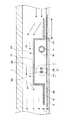
以下、添付の図面を参照しながら、本発明の限定的でない例示の実施形態について説明する。添付の全図面中、同一又は対応する部材又は部品については、同一又は対応する参照符号を付し、重複する説明を省略する。また、図面は、部材もしくは部品間の相対比を示すことを目的とせず、したがって、具体的な厚さや寸法は、以下の限定的でない実施形態に照らし、当業者により決定されるべきものである。 Hereinafter, exemplary embodiments of the present invention will be described with reference to the accompanying drawings. In all the attached drawings, the same or corresponding members or parts are denoted by the same or corresponding reference numerals, and redundant description is omitted. Also, the drawings are not intended to show relative ratios between members or parts, and therefore specific thicknesses and dimensions should be determined by those skilled in the art in light of the following non-limiting embodiments. .
図1から図3までを参照すると、本発明の実施形態による成膜装置は、ほぼ円形の平面形状を有する扁平な真空容器1と、この真空容器1内に設けられ、真空容器1の中心に回転中心を有する回転テーブル2と、を備えている。真空容器1は、有底の円筒形状を有する容器本体12と、容器本体12の上面に対して、例えばOリングなどのシール部材13(図1)を介して気密に着脱可能に配置される天板11とを有している。 Referring to FIGS. 1 to 3, a film forming apparatus according to an embodiment of the present invention is a
回転テーブル2は、中心部にて円筒形状のコア部21に固定され、このコア部21は、鉛直方向に伸びる回転軸22の上端に固定されている。回転軸22は真空容器1の底部14を貫通し、その下端が回転軸22(図1)を鉛直軸回りに回転させる駆動部23に取り付けられている。回転軸22及び駆動部23は、上面が開口した筒状のケース体20内に収納されている。このケース体20はその上面に設けられたフランジ部分が真空容器1の底部14の下面に気密に取り付けられており、ケース体20の内部雰囲気と外部雰囲気との気密状態が維持されている。 The rotary table 2 is fixed to a
回転テーブル2の表面部には、図2及び図3に示すように回転方向(周方向)に沿って複数(図示の例では5枚)の基板である半導体ウエハ(以下「ウエハ」という)Wを載置するための円形状の凹部24が設けられている。なお図3には便宜上1個の凹部24だけにウエハWを示す。この凹部24は、ウエハWの直径よりも僅かに例えば4mm大きい内径と、ウエハWの厚さにほぼ等しい深さとを有している。したがって、ウエハWを凹部24に載置すると、ウエハWの表面と回転テーブル2の表面(ウエハWが載置されない領域)とが同じ高さになる。凹部24の底面には、ウエハWの裏面を支えてウエハWを昇降させるための例えば3本の昇降ピンが貫通する貫通孔(いずれも図示せず)が形成されている。 As shown in FIGS. 2 and 3, a semiconductor wafer (hereinafter referred to as “wafer”) W that is a plurality of (five in the illustrated example) substrates along the rotation direction (circumferential direction) is provided on the surface portion of the
図2及び図3に示すように、回転テーブル2の上方には、各々例えば石英からなる反応ガスノズル31、反応ガスノズル32、分離ガスノズル41,42、及び活性化ガスインジェクタ220が真空容器1の周方向(回転テーブル2の回転方向)に互いに間隔をおいて配置されている。図示の例では、後述の搬送口15から時計回り(回転テーブル2の回転方向)に活性化ガスインジェクタ220、分離ガスノズル41、反応ガスノズル31、分離ガスノズル42、及び反応ガスノズル32がこの順番で配列されており、これらの活性化ガスインジェクタ220及びノズル31、32、41、42は、各ノズル31、32、41、42の基端部であるガス導入ポート31a、32a、41a、42aを容器本体12の外周壁に固定することにより、真空容器1の外周壁から真空容器1内に導入され、容器本体12の半径方向に沿って回転テーブル12に対して水平に伸びるように取り付けられている。活性化ガスインジェクタ220については後に説明する。 As shown in FIGS. 2 and 3, a
反応ガスノズル31は、不図示の配管及び流量調整器などを介して、第1の反応ガスとしてのSi(シリコン)含有ガスの供給源(図示せず)に接続されている。反応ガスノズル32は、不図示の配管及び流量調整器などを介して、第2の反応ガスとしての酸化ガスの供給源(図示せず)に接続されている。分離ガスノズル41、42は、いずれも不図示の配管及び流量調整バルブなどを介して、分離ガスとしての窒素(N2)ガスの供給源(図示せず)に接続されている。The
Si含有ガスとしては、例えば有機アミノシランガスを用いることができ、酸化ガスとしては、例えばO3(オゾン)ガス若しくはO2(酸素)ガス又はこれらの混合ガスを用いることができる。As the Si-containing gas, for example, an organic aminosilane gas can be used, and as the oxidizing gas, for example, O3 (ozone) gas, O2 (oxygen) gas, or a mixed gas thereof can be used.
反応ガスノズル31、32には、回転テーブル2に向かって開口する複数のガス吐出孔33が、反応ガスノズル31、32の長さ方向に沿って、例えば10mmの間隔で配列されている。反応ガスノズル31の下方領域は、Si含有ガスをウエハWに吸着させるための第1の処理領域P1となる。反応ガスノズル32の下方領域は、第1の処理領域P1においてウエハWに吸着されたSi含有ガスを酸化させる第2の処理領域P2となる。
図2及び図3を参照すると、分離ガスノズル41、42とともに分離領域Dを構成する、天板11の裏面から回転テーブル2に向かって突出する凸状部4が真空容器1に設けられている。凸状部4は、頂部が円弧状に切断された扇型の平面形状を有し、本実施形態においては、内円弧が突出部5(後述)に連結し、外円弧が、真空容器1の容器本体12の内周面に沿うように配置されている。In the
Referring to FIGS. 2 and 3, the
反応ガスノズル31から反応ガスノズル32まで回転テーブル2の同心円に沿った真空容器1の断面を示す図4を参照すると、真空容器1内には、凸状部4によって、凸状部4の下面である平坦な低い天井面44(第1の天井面)と、この天井面44の周方向両側に位置する、天井面44よりも高い天井面45(第2の天井面)とが存在する。天井面44は、頂部が円弧状に切断された扇型の平面形状を有している。また、図示のとおり、凸状部4には周方向中央において、半径方向に伸びるように形成された溝部43が形成され、分離ガスノズル42が溝部43内に収容されている。もう一つの凸状部4にも同様に溝部43が形成され、ここに分離ガスノズル41が収容されている。また、高い天井面45の下方の空間に反応ガスノズル31、32がそれぞれ設けられている。これらのノズル31、32は、天井面45から離間してウエハWの近傍に設けられている。なお、説明の便宜上、図4に示すように、反応ガスノズル31が設けられる、高い天井面45の下方の空間を空間481とし、反応ガスノズル32が設けられる、高い天井面45の下方の空間を空間482とする。 Referring to FIG. 4 showing a cross section of the
天井面44は、回転テーブル2に対し、狭隘な空間である分離空間Hを形成している。分離空間Hは、第1の領域P1からのSi含有ガスと、第2の領域P2からの酸化ガスとを分離することができる。具体的には、分離ガスノズル42からN2ガスを吐出すると、N2ガスは、分離空間Hを通して空間481及び空間482へ向かって流れる。このとき、空間481及び482に比べて容積の小さい分離空間HをN2ガスが流れるため、分離空間Hの圧力は空間481及び482の圧力に比べて高くすることができる。すなわち、空間481と482の間に圧力障壁が形成される。また、分離空間Hから空間481及び482へ流れ出るN2ガスが、第1の領域P1からのSi含有ガスと、第2の領域P2からの酸化ガスとに対するカウンターフローとして働く。したがって、Si含有ガスも酸化ガスも分離空間Hへ流入することは殆どできない。よって、真空容器1内においてSi含有ガスと酸化ガスとが混合し、反応することが抑制される。The
一方、天板11の下面には、図2及び図3に示すように、回転テーブル2を固定するコア部21の外周を囲む突出部5が設けられている。この突出部5は、本実施形態においては、凸状部4における回転中心側の部位と連続しており、その下面が天井面44と同じ高さに形成されている。 On the other hand, as shown in FIGS. 2 and 3, a
なお、図2及び図3においては、説明の便宜上、天井面45よりも低くかつ分離ガスノズル41、42よりも高い位置にて容器本体12が切断されているように、容器本体12及びその内部を示している。 2 and 3, for convenience of explanation, the
先に参照した図1は、図3のI−I'線に沿った断面図であり、天井面45が設けられている領域を示している一方、図5は、天井面44が設けられている領域を示す断面図である。図5に示すように、扇型の凸状部4の周縁部(真空容器1の外縁側の部位)には、回転テーブル2の外端面に対向するようにL字型に屈曲する屈曲部46が形成されている。この屈曲部46は、凸状部4と同様に、分離領域Dの両側から反応ガスが侵入することを抑制して、両反応ガスの混合を抑制する。扇型の凸状部4は天板11に設けられ、天板11が容器本体12から取り外せるようになっていることから、屈曲部46の外周面と容器本体12との間には僅かに隙間がある。屈曲部46の内周面と回転テーブル2の外端面との隙間、及び屈曲部46の外周面と容器本体12との隙間は、例えば回転テーブル2の表面に対する天井面44の高さと同様の寸法に設定されている。 FIG. 1 referred to above is a cross-sectional view taken along the line II ′ of FIG. 3 and shows a region where the
容器本体12の内周壁は、分離領域Dにおいては図4に示すように屈曲部46の外周面と接近して垂直面に形成されているが、分離領域D以外の部位においては、図1に示すように例えば回転テーブル2の外端面と対向する部位から底部14に亘って外方側に窪んでいる。以下、説明の便宜上、矩形の断面形状を有する、この窪んだ部分を排気領域と記す。具体的には、第1の処理領域P1に連通する排気領域を第1の排気領域E1と記し、第2の処理領域P2に連通する領域を第2の排気領域E2と記す。これらの第1の排気領域E1及び第2の排気領域E2の底部には、図1から図3に示すように、それぞれ、第1の排気口610及び第2の排気口620が形成されている。第1の排気口610及び第2の排気口620は、図1に示すように各々排気管630を介して真空排気手段である例えば真空ポンプ640に接続されている。なお図1中、参照符号650は圧力調整手段である。 As shown in FIG. 4, the inner peripheral wall of the container
回転テーブル2と真空容器1の底部14との間の空間には、図1及び図4に示すように加熱手段であるヒータユニット7が設けられ、回転テーブル2を介して回転テーブル2上のウエハWが、プロセスレシピで決められた温度(例えば450℃)に加熱される。回転テーブル2の周縁付近の下方側には、回転テーブル2の上方空間から排気領域E1、E2に至るまでの雰囲気とヒータユニット7が置かれている雰囲気とを区画して回転テーブル2の下方領域へのガスの侵入を抑えるために、リング状のカバー部材71が設けられている(図5)。このカバー部材71は、回転テーブル2の外縁部及び外縁部よりも外周側を下方側から臨むように設けられた内側部材71aと、この内側部材71aと真空容器1の内壁面との間に設けられた外側部材71bと、を備えている。外側部材71bは、分離領域Dにおいて凸状部4の外縁部に形成された屈曲部46の下方にて、屈曲部46と近接して設けられ、内側部材71aは、回転テーブル2の外縁部下方(及び外縁部よりも僅かに外側の部分の下方)において、ヒータユニット7を全周に亘って取り囲んでいる。 As shown in FIGS. 1 and 4, a heater unit 7 serving as a heating unit is provided in the space between the
ヒータユニット7が配置されている空間よりも回転中心寄りの部位における底部14は、回転テーブル2の下面の中心部付近におけるコア部21に接近するように上方側に突出して突出部12aをなしている。この突出部12aとコア部21との間は狭い空間になっており、また底部14を貫通する回転軸22の貫通穴の内周面と回転軸22との隙間が狭くなっていて、これら狭い空間はケース体20に連通している。そしてケース体20にはパージガスであるN2ガスを狭い空間内に供給してパージするためのパージガス供給管72が設けられている。また真空容器1の底部14には、ヒータユニット7の下方において周方向に所定の角度間隔で、ヒータユニット7の配置空間をパージするための複数のパージガス供給管73が設けられている(図5には一つのパージガス供給管73を示す)。また、ヒータユニット7と回転テーブル2との間には、ヒータユニット7が設けられた領域へのガスの侵入を抑えるために、外側部材71bの内周壁(内側部材71aの上面)から突出部12aの上端部との間を周方向に亘って覆う蓋部材7aが設けられている。蓋部材7aは例えば石英で作製することができる。The
また、真空容器1の天板11の中心部には分離ガス供給管51が接続されていて、天板11とコア部21との間の空間52に分離ガスであるN2ガスを供給するように構成されている。この空間52に供給された分離ガスは、突出部5と回転テーブル2との狭い隙間50を介して回転テーブル2のウエハ載置領域側の表面に沿って周縁に向けて吐出される。空間50は分離ガスにより空間481及び空間482よりも高い圧力に維持され得る。したがって、空間50により、第1の処理領域P1に供給されるSi含有ガスと第2の処理領域P2に供給される酸化ガスとが、中心領域Cを通って混合することが抑制される。すなわち、空間50(又は中心領域C)は分離空間H(又は分離領域D)と同様に機能することができる。Further, a separation
さらに、真空容器1の側壁には、図2、図3に示すように、外部の搬送アーム10と回転テーブル2との間で基板であるウエハWの受け渡しを行うための搬送口15が形成されている。この搬送口15は図示しないゲートバルブにより開閉される。また回転テーブル2におけるウエハ載置領域である凹部24はこの搬送口15に臨む位置にて搬送アーム10との間でウエハWの受け渡しが行われることから、回転テーブル2の下方側において受け渡し位置に対応する部位に、凹部24を貫通してウエハWを裏面から持ち上げるための受け渡し用の昇降ピン及びその昇降機構(いずれも図示せず)が設けられている。 Further, as shown in FIGS. 2 and 3, a
次に、図3、図6、及び図7を参照しながら、活性化ガスインジェクタ220について説明する。活性化ガスインジェクタ220は、ウエハW上に成膜された膜に対して活性化された改質ガス及びエッチングガスを供給し、その膜を改質するとともにエッチングすることができる。図6及び図7に示すように、活性化ガスインジェクタ220には、改質ガス及びエッチングガスを真空容器1内に供給する改質ガス供給部として機能するガス導入ノズル34が設けられている。ガス導入ノズル34は、ガス導入ノズル34の長さ方向に沿って所定の間隔で形成された複数のガス孔341を有している。ガス導入ノズル34は例えば石英ガラスで作製することができる。また、ガス導入ノズル34よりも回転テーブル2の回転方向下流側には、ガス導入ノズル34から導入される改質ガス及びエッチングガスをプラズマ化するために、互いに平行な1対の棒状のシース管35a、35bからなるプラズマ発生部80が配置されている。シース管35a、35bは、互いに平行となるように設けられており、互いに等しい長さを有している。
ガス導入ノズル34及びプラズマ発生部80は、回転テーブル2のほぼ中心に向かう方向、かつ回転テーブル2の接線方向に直交する方向に、回転テーブル2の上面と平行に延びている。また、ガス導入ノズル34及びプラズマ発生部80は、容器本体12の外周面に取り付けられた導入管80aにより、真空容器1内の気密が維持されるように支持されている。Next, the activated
The
図3に示すように、ガス導入ノズル34には、ガス導入管271の一端が接続され、ガス導入管271の他端には、改質ガス導入管251とエッチングガス導入管261が接続されている。改質ガス導入管251には、開閉バルブ252及び流量調整器253を介して、改質ガスが貯留された改質ガス供給源254が接続されている。改質ガスとしては、例えば酸素(O2)ガスを使用することができ、O2ガスに代えて又はO2ガスとともに、例えばアルゴン(Ar)ガスまたはヘリウム(He)ガスなどの希ガスを用いても良い。また、エッチングガス導入管261には、開閉バルブ262及び流量調整器263を介して、エッチングガスが貯留されたエッチングガス供給源264が接続されている。エッチングガスとしては、エッチング対象膜をエッチング可能なガスを用いることができ、本実施形態においては、酸化シリコン膜をエッチングする例えばトリフルオロメタン(CHF3)などのハイドロフルオロカーボン、四フッ化メタン(CF4)などのフルオロカーボン等のフッ素系ガスを用いることができる。As shown in FIG. 3, one end of a
一方、プラズマ発生部80は、図7に示すように、互いに平行に延びるシース管35a、35bと、シース管35a内に挿入されている電極36aと、シース管35b内に挿入されている電極36bとを有している。シース管35a、35bは、例えば石英、アルミナ(酸化アルミニウム)、又はイットリア(酸化イットリウム、Y2O3)等の絶縁体により作製されている。電極36a、36bは、平行電極として機能し、例えばニッケル合金やチタンなどから作製されている。図3に示すように、電極36a、36bには、整合器225を介して高周波電源224が接続されている。例えば13.56MHz、例えば500Wの高周波電力が高周波電源224から電極36a、36bに供給される。なお、シース管35a、35bは、図7に示すように、基端側(真空容器1の内壁側)において保護管37に挿入されている。保護管37は図5などでは省略されている。また、図6以外では、シース管35a、35bを簡略化している。On the other hand, as shown in FIG. 7, the
図6及び図7に示すように、容器本体12の内部において、活性化ガスインジェクタ220には、ガス導入ノズル34及びシース管35a、35bを覆うカバー体221が設けられている。カバー体221は例えば石英などの絶縁体により作製されている。また、カバー体221における回転テーブル2のほぼ半径方向に延びる下端縁には気流規制板222が取り付けられている。気流規制板222は、カバー体221と同様に例えば石英ガラスなどの絶縁体により作製されている。また、カバー体221は、気流規制板22の下面と回転テーブル2の上面との間隔t(図7)が、この間隔tを通してカバー体221の内部へガスが流入するのを抑制できる程度に小さくなるように、例えば天板11の下面から吊り下げられている。さらに、気流規制板222の幅u(図7)は、回転テーブル2の外周に向かう方向に沿って広がっている。回転テーブル2の外周側においては、ガスの回転方向に沿った流速が速くなるが、気流規制板22の幅uが外周に向かうほど広くなっているため、カバー体221の内部へのガスの流入を抑制することができる。 As shown in FIGS. 6 and 7, inside the container
また、本実施形態による成膜装置には、装置全体の動作のコントロールを行うためのコンピュータからなる制御部100が設けられており、この制御部100のメモリ内には、制御部100の制御の下に、後述する成膜方法を成膜装置に実施させるプログラムが格納されている。このプログラムは後述の装置の動作を実行するようにステップ群が組まれており、ハードディスク、コンパクトディスク、光磁気ディスク、メモリカード、フレキシブルディスクなどの記憶部101から制御部100内にインストールされる。 In addition, the film forming apparatus according to the present embodiment is provided with a
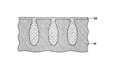
次に、本発明の実施形態による成膜方法について本実施形態による成膜装置を用いて行う場合を例にとり説明する。以下では、反応ガスノズル32から供給される酸化ガスとしてO3ガスを用い、活性化ガスインジェクタ220から供給される改質ガスとしてO2ガスとArガスとの混合ガス(以下、O2/Arガスと記す)、エッチングガスとしてCHF3ガスを用いることとする。また、使用するウエハWには図8A(a)に示すようなライン・スペース・パターンが形成されているものとし、スペースSを酸化シリコンで埋め込む場合を説明する。スペースSは、凹状に湾曲した側壁を有し、上端及び底部に比べて、これらの間における幅が広くなっている。Next, the film forming method according to the embodiment of the present invention will be described by taking as an example the case where the film forming apparatus according to the present embodiment is used. Hereinafter, O3 gas is used as the oxidizing gas supplied from the
(ウエハの搬入ステップ)
先ず、図示しないゲートバルブを開き、外部から搬送アーム10により搬送口15を介してウエハWを回転テーブル2の凹部24内に受け渡す。この受け渡しは、凹部24が搬送口15に臨む位置に停止したときに凹部24の底面の貫通孔を介して真空容器1の底部側から不図示の昇降ピンが昇降することにより行われる。このようなウエハWの受け渡しを回転テーブル2を間欠的に回転させて行い、回転テーブル2の5つの凹部24内に夫々ウエハWを載置する。(Wafer loading step)
First, a gate valve (not shown) is opened, and the wafer W is transferred from the outside to the
(保護層成膜ステップ)
続いてゲートバルブを閉じ、真空ポンプ640により真空容器1内を引き切りの状態にした後、分離ガスノズル41、42から分離ガスであるN2ガスを所定の流量で吐出し、分離カス供給管51及びパージガス供給管72、72からもN2ガスを所定の流量で吐出する。これに伴い、圧力調整手段650により真空容器1内を予め設定した処理圧力に調整する。次いで、回転テーブル2を時計回りに例えば20rpmの回転速度で回転させながらヒータユニット7によりウエハWを例えば450℃に加熱する。(Protective layer deposition step)
Subsequently, the gate valve is closed, and the inside of the
この後、反応ガスノズル31、32から夫々Si含有ガス及びO3ガスを吐出する。また、ガス導入ノズル34からO2/Arガスのみを吐出し、夫々のシース管35a、35b間に13.56MHzの周波数を有する高周波を400Wの電力で供給する。これにより、活性化ガスインジェクタ220のカバー体221の内部空間(プラズマ発生部80近傍)において酸素プラズマが生成される。Thereafter, the Si-containing gas and the O3 gas are discharged from the
回転テーブル2の回転により、ウエハWは、第1の処理領域P1、分離領域D、第2の処理領域P2、改質領域150(活性化ガスインジェクタ220の下方領域、図3及び図6参照)、分離領域Dを通過する。第1の処理領域P1において、図8A(b)に示すように、ウエハWの表面並びにスペースS内の側壁及び底部にSi含有ガスが吸着し、Si含有ガス分子層61が形成され、第2の処理領域P2において、図8A(c)に示すように、ウエハW上に吸着したSi含有ガスがO3ガスにより酸化されて1又は複数分子層の酸化シリコン膜62が堆積される。Due to the rotation of the
酸化シリコン膜62中には、例えばSi含有ガス中に含まれる残留基のため、水分(OH基)や有機物などの不純物が含まれている場合がある。しかしながら、ウエハWが改質領域150に到達すると、酸素プラズマにより酸化シリコン膜62が改質される。具体的には、酸化シリコン膜62が酸素プラズマに曝されることにより、例えば酸化シリコン膜中に残る有機不純物が酸化されて気相中に放出されたり、プラズマ中の高エネルギー粒子の衝撃により酸化シリコン膜内の元素が再配列されて酸化シリコン膜の緻密化(高密度化)が図られたりすることになる。このようにウエハW(回転テーブル2)が1回転する間に、1又は複数分子層の酸化シリコン膜62が堆積され改質されて、高品位な酸化シリコン膜63(図8A(d))がウエハWに形成される。その後、ウエハWの回転を所定の回数繰り返すと、酸化シリコン膜63は、所定の膜厚(例えば5nmから100nm)を有するに至る。ここまでのステップで得られる酸化シリコン膜は、ウエハWの表面及びスペースSの内壁が、後に供給されるエッチングガスにより腐食されるのを防ぐ保護層として機能する。 The
(第1のステップ)
次に、活性化ガスインジェクタ220のガス導入ノズル34からO2/Arガスに加えてCHF3ガスを供給し、ウエハWの回転を更に継続することにより、図8A(a)から(d)を参照しながら説明したSi含有ガスの吸着、O3ガスによるSi含有ガスの酸化、及び酸化シリコン膜の改質を繰り返す。この場合には、堆積された酸化シリコン膜62が改質されるとともに、電極36a、36b間に供給される高周波によりCHF3ガスが活性化されるため、酸化シリコン膜62、63がエッチングされる。すなわち、第1のステップにおいては、酸化シリコンの堆積とエッチングとが、堆積速度>エッチング速度となるように同時に行われる。また、このとき、CHF3ガスの供給量、真空容器1内の圧力、高周波電力などの成膜条件は、酸化シリコン膜のエッチング速度が、スペースSの開口付近で大きく、スペースSの底部側で小さくなるように(換言すると、酸化シリコン膜の堆積速度が、スペースSの開口付近で遅く底部側で速くなるように)設定される。このような条件は、予備実験等から予め決定することができる。そのような条件によれば、スペースSの開口が酸化シリコンで塞がれることなく、酸化シリコンの堆積が継続される。(First step)
Next, CHF3 gas is supplied from the
(第2のステップ)
所定の回数ウエハWが回転すると、スペースSの側壁及び底部に堆積される酸化シリコン膜64の断面は、概ね、図8B(e)に示すようになる。すなわち、スペースSの底部側での膜厚は、スペースSの開口付近及びウエハWの表面における膜厚よりも厚くなり、スペースSの側壁において、僅かに凹状に湾曲している(凹状の湾曲の程度は、元のスペースSの側壁における凹状の湾曲の程度よりも軽減されている)。(Second step)
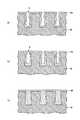
When the wafer W is rotated a predetermined number of times, the cross section of the
次に、回転テーブル2の回転、ウエハWの加熱、反応ガスノズル32からのO3ガスの供給、活性化ガスインジェクタ220のガス導入ノズル34からのO2/Arガス及びCHF3ガスの供給、及び活性化ガスインジェクタ220の電極36a、36bへの高周波の供給などを第1のステップのときと同じ条件で継続しつつ、反応ガスノズル31からのSi含有ガスの供給のみを停止する。このため、酸化シリコンの堆積が停止されるが、酸化シリコン膜64のエッチングは継続される。酸化シリコン膜64のエッチング速度は、スペースSの開口付近で速く底部側で遅いため、所定の時間が経過した後、酸化シリコン膜64は、図8(f)に示すように、スペースSは、開口が広く底部に向かって幅が狭くなるテーパ状の断面形状を有することとなる。なお、このエッチングの時間は、ウエハWの上面及びスペースSの開口付近でウエハWが露出しない程度に、例えば予備実験等から決定することができる。Next, rotation of the
(第3のステップ)
次に、反応ガスノズル31からのSi含有ガスの供給を再開する。これにより、第1のステップと同様に酸化シリコンの堆積とエッチングとが同時に行われることとなる。すなわち、ウエハWが第1の処理領域P1を通過する際に、図8C(g)に示すように、テーパ状の断面形状を有するスペースSの内面にSi含有ガスが吸着してSi含有ガス分子層61が形成され、処理領域P2を通過する際に、Si含有ガス分子層61がO3ガスにより酸化されて酸化シリコン膜62が形成され、処理領域150を通過する際に、酸化シリコン膜62が改質されるとともにエッチングされて、改質された酸化シリコン膜63が得られる。これを継続していくと、スペースSの両方の側壁に形成される酸化シリコン膜63が互いに近づくことにより、スペースSが埋め込まれるよりもむしろ、テーパ角度が小さくなるように、換言すると、スペースSの底部から酸化シリコン膜63が厚くなるようにしてスペースSが埋め込まれていく。そして、所定の時間が経過すると、図8Dに示すように、ボイドが形成されることなく、スペースSが酸化シリコン膜66で埋め込まれるに至る。(Third step)
Next, the supply of the Si-containing gas from the
以降、反応ガスノズル31からのSi含有ガスの供給、反応ガスノズル32からのO3ガスの供給、活性化ガスインジェクタ220のガス導入ノズル34からのO2/Arガス及びCHF3ガスの供給、並びに活性化ガスインジェクタ220の電極36a、36bへの高周波の供給を停止し、真空容器1内をN2ガスによりパージした後、ウエハ搬入ステップにおける手順と逆の手順によりウエハWが真空容器1から搬出される。以上により、本実施形態による酸化シリコン膜の成膜方法が終了する。Thereafter, supply of Si-containing gas from the
以上説明したとおり、本実施形態においては、反応ガスノズル31、反応ガスノズル32、及び活性化ガスインジェクタ220が一つの真空容器1内に設けられた成膜装置において、反応ガスノズル31からSi含有ガスが供給される第1の処理領域P1と、反応ガスノズル32からO3ガスが供給される第2の処理領域P2と、酸素プラズマ及び活性化されたCHF3ガスが供給される処理領域150とを、回転テーブル2の回転によりウエハWが通過する。このため、第1の処理領域P1においてウエハWに吸着するSi含有ガスが、第2の処理領域P2においてO3ガスにより酸化され、ウエハW上に酸化シリコン膜62が形成される。この酸化シリコン膜62は、処理領域150において酸素プラズマにより改質されるとともに、活性化されたCHF3ガスによりエッチングされる(第1のステップ)。このとき、酸化シリコン膜63の堆積速度は、見かけ上、スペースSの開口付近で遅く底部で速いため、スペースSの開口が塞がり難い。したがって、スペースS内が埋め込まれる前に、スペースSの開口が塞がってしまうと、スペースS内にはボイドが形成されることとなるが、本実施形態によれば、ボイドの形成を軽減することが可能となる。As described above, in the present embodiment, the Si-containing gas is supplied from the
また、本実施形態においては、第2のステップとして、Si含有ガスの供給を停止してエッチングが行われ、スペースSの断面を、底部から開口に向かう方向に沿って幅が広がるテーパ状にすることができる(図8B(f)参照)。この後、第1のステップと同様の第3のステップを行うと、スペースSは、スペースSの底部に堆積される酸化シリコン膜の膜厚が厚くなるように埋め込まれる。 In the present embodiment, as a second step, the supply of the Si-containing gas is stopped and etching is performed, and the cross section of the space S is tapered so that the width increases in the direction from the bottom toward the opening. (See FIG. 8B (f)). Thereafter, when a third step similar to the first step is performed, the space S is embedded so that the thickness of the silicon oxide film deposited on the bottom of the space S is increased.
なお、ALDによりスペースを酸化シリコンで埋め込もうとすると、スペースの両方の側壁に成膜される酸化シリコン膜の表面が互いに近づいていき、互いに接触してスペースが埋め込まれる傾向がある。このような場合、特に、両側から酸化シリコン膜の表面が接する直前においては両者間の隙間が極めて狭いため、副生成物が外部へ排気され難くなる。そのため、副生成物が酸化シリコン中に取り込まれてしまう可能性がある。この場合、互いの表面が接触した界面(シーム)においては不純物濃度が高くなったり、シームにおいて酸素原子とシリコン原子との間の結合手が形成されずに多数の欠陥が生成されたりするおそれがある。すなわち、このようなシーム近傍においては、酸化シリコンの膜質が悪化している可能性がある。この場合、例えば後のエッチング工程において、シームに沿ってエッチングが速く進行して溝が形成される可能性がある。 Note that, when an ALD is used to fill a space with silicon oxide, the surfaces of the silicon oxide films formed on both side walls of the space tend to approach each other, and the space tends to be buried in contact with each other. In such a case, particularly, immediately before the surface of the silicon oxide film comes into contact from both sides, the gap between the two is extremely narrow, so that the by-product is hardly exhausted to the outside. Therefore, there is a possibility that by-products are taken into silicon oxide. In this case, there is a possibility that the impurity concentration is high at the interface (seam) where the surfaces are in contact with each other or a large number of defects are generated without the formation of bonds between oxygen atoms and silicon atoms in the seam. is there. That is, in the vicinity of such a seam, the film quality of silicon oxide may be deteriorated. In this case, for example, in the subsequent etching process, there is a possibility that the etching proceeds fast along the seam to form a groove.
しかし、本実施形態による成膜方法によれば、スペースSの両側壁に堆積される酸化シリコン膜の表面が互いに近づきあってシームを形成するのが抑制されるため、シーム面及びその近傍における酸化シリコンの性質の悪化を抑制することができる。 However, according to the film forming method according to the present embodiment, the surfaces of the silicon oxide films deposited on the both side walls of the space S are prevented from approaching each other to form a seam. Deterioration of the properties of silicon can be suppressed.
また、反応ガスノズル31、反応ガスノズル32、及び活性化ガスインジェクタ220が一つの真空容器1内に設けられた本発明の実施形態による成膜装置において本発明の実施形態による成膜方法を実施することにより、酸化シリコン膜の堆積、改質、及びエッチングを一つの真空容器1内で行うことができる。したがって、堆積とエッチングを異なる装置で行う場合に比べ、ウエハWの搬送時間の必要が無いため、スループットを向上できるという利点がある。また、反応ガスノズル31からSi含有ガスがウエハWの表面に吸着し、吸着されたSi含有ガスが酸化ガスにより酸化されて酸化シリコンの分子層が形成された直後に改質を行うことができるため、活性化された改質ガスは、分子層レベルの膜厚を有する酸化シリコン膜に対して作用することとなり、改質効率が向上される。 In addition, the film forming method according to the embodiment of the present invention is performed in the film forming apparatus according to the embodiment of the present invention in which the
なお、図8A(a)から図8Dまでを参照しながら、図8A(a)に示すような側壁が凹状に湾曲したスペースSを埋め込む場合について説明したが、本実施形態による成膜方法は、そのようなスペースSにのみ適用されるものではない。例えば、図9に示すように側壁が平坦な矩形の断面形状を有するスペースSについても、ボイドの形成を抑制しつつ埋め込むことができる。すなわち、まず、上述のウエハ搬入ステップから第1のステップまでを行って所定の膜厚を有する(改質されて高品位な)酸化シリコン膜64(図9(a)参照)が堆積される。次に、第2のステップを行うと、図9(b)に示すように、底部から開口に向かう方向に沿って幅が広がるテーパ状のスペースが形成される。そして、第3のステップを行うと、ボイドが形成されることなく、ウエハWのスペースが酸化シリコン膜66により埋め込まれ得る。 8A (a) to FIG. 8D, the case where the space S whose side wall is curved in a concave shape as shown in FIG. 8A (a) has been described. However, the film forming method according to the present embodiment is It is not applied only to such a space S. For example, as shown in FIG. 9, a space S having a rectangular cross-sectional shape with a flat side wall can be embedded while suppressing the formation of voids. That is, first, the silicon oxide film 64 (see FIG. 9A) having a predetermined film thickness (modified and high quality) is deposited by performing the above-described wafer carry-in step to the first step. Next, when a 2nd step is performed, as shown in FIG.9 (b), the taper-shaped space which a width spreads along the direction which goes to an opening from a bottom part is formed. Then, when the third step is performed, the space of the wafer W can be filled with the
さらに、図10に示す、底部から開口に向かう方向に沿って幅が狭くなる逆テーパ状のスペースを埋め込むことも可能である。すなわち、まず、上述のウエハ搬入ステップから第1のステップまでを行って所定の膜厚を有する(改質されて高品位な)酸化シリコン膜64(図10(a)参照)が堆積される。図示のとおり、活性化ガスインジェクタ220によってエッチングも行われるため、スペースSの逆テーパ状の断面形状は緩和されている。次に、第2のステップを行った後に、図10(b)に示すように、スペースSの断面形状がほぼ矩形となったとする。このような矩形の断面形状は、図9(a)示すウエハWに形成されるスペーサSの断面形状とほぼ同様である。したがって、図9(a)から図(c)までを参照しながら説明した成膜方法を行うことにより、図10(c)に示すように逆テーパ状の断面を有するスペースSもまた埋め込むことができる。すなわち、この場合には、上述のウエハ搬入ステップから第1のステップを行った後、第2のステップ、第3のステップ(第1のステップと実質的に同一)、第2のステップ、及び第3のステップが行われることとなる。換言すると、本実施形態による成膜方法において、第2のステップの回数は1回に限られることなく、第1のステップ(又は第3のステップ)と交互に複数回行っても良い。 Furthermore, it is also possible to embed an inversely tapered space whose width becomes narrower along the direction from the bottom toward the opening, as shown in FIG. That is, first, the silicon oxide film 64 (see FIG. 10A) having a predetermined film thickness (modified and high quality) is deposited by performing the above-described wafer carry-in step to the first step. As shown in the drawing, since etching is also performed by the activated
ここで各ステップにおける成膜条件を例示すると、以下のとおりである。ただし、以下の成膜条件は本発明を限定するものではない。成膜条件は、使用する成膜装置の形状やサイズ、成膜する膜の材質、使用する反応ガス、改質ガス、及びエッチングガスに応じて適宜決定されるべきものである。
(1)保護層成膜ステップ
・回転テーブル2の回転速度: 1rpm〜500rpm(300mm径のウエハWを用いる場合)
・真空容器1内の圧力: 133Pa(1Torr)
・反応ガスノズル31からのSi含有ガスの流量: 100sccm
・反応ガスノズル32からのO3ガスの流量: 10000sccm
・活性化ガスインジェクタ220からのO2/Arガスの流量: 10000sccm(O2ガス流量: 1000sccm、Arガス流量: 9000sccm)
・活性化ガスインジェクタ220へ供給される高周波電力: 500〜900W(周波数13.56MHz)
・回転テーブル2の回転速度: 1から500rpm
(2)第1のステップ及び第3のステップ
・活性化ガスインジェクタ220からのCHF3ガスの流量: 0.5〜3sccm
・回転テーブル2の回転速度: 1から500rpm
(その他の条件は、保護層成膜ステップと同じ)
(3)第2のステップ
・反応ガスノズル31からのSi含有ガスの流量: 0sccm
(その他の条件は、第1のステップ及び第3のステップと同じ)
以上、実施形態を参照しながら本発明を説明したが、本発明は開示された実施形態に限定されさるものではなく、添付の特許請求の範囲内で種々の変形や変更が可能である。Here, the film forming conditions in each step are exemplified as follows. However, the following film forming conditions do not limit the present invention. The film forming conditions should be appropriately determined according to the shape and size of the film forming apparatus used, the material of the film to be formed, the reaction gas used, the reforming gas, and the etching gas.
(1) Protective layer deposition step / Rotation speed of turntable 2: 1 rpm to 500 rpm (when using 300 mm diameter wafer W)
-Pressure in the vacuum vessel 1: 133 Pa (1 Torr)
-Flow rate of Si-containing gas from the reaction gas nozzle 31: 100 sccm
-Flow rate of O3 gas from the reaction gas nozzle 32: 10,000 sccm
O2 / Ar gas flow rate from the activated gas injector 220: 10,000 sccm (O2 gas flow rate: 1000 sccm, Ar gas flow rate: 9000 sccm)
High frequency power supplied to the activated gas injector 220: 500 to 900 W (frequency 13.56 MHz)
・ Rotational speed of rotary table 2: 1 to 500 rpm
(2) First step and third step-CHF3 gas flow rate from the activated gas injector 220: 0.5-3 sccm
・ Rotational speed of rotary table 2: 1 to 500 rpm
(Other conditions are the same as the protective layer deposition step)
(3) Second step-Si-containing gas flow rate from the reactive gas nozzle 31: 0 sccm
(Other conditions are the same as the first step and the third step)
The present invention has been described above with reference to the embodiments. However, the present invention is not limited to the disclosed embodiments, and various modifications and changes can be made within the scope of the appended claims.
例えば、底部から開口に向かう方向に沿って幅が広がるテーパ状の断面形状を有するスペースを酸化シリコンで埋め込む場合には、第2のステップを行わずに、第1のステップにおける堆積(改質を含んでもよい、以下同じ)と同時のエッチングだけでも埋め込み得る。また、そのようなスペースにおいては、第1のステップ及び第3のステップにおいては堆積のみ行い、第2のステップでのエッチングを行うことにより埋め込むことが可能である。 For example, in the case where a space having a tapered cross-sectional shape whose width increases in the direction from the bottom toward the opening is filled with silicon oxide, the deposition (modification in the first step is performed without performing the second step). It may be embedded only by etching at the same time as the same may be included. Further, in such a space, it is possible to embed by performing only deposition in the first step and the third step and performing etching in the second step.
また、プラズマ発生手段80は、2つ以上設けても良い。更に、既述のように平行電極(電極36a、36b)を用いて容量結合型プラズマを発生させたが、コイル型の電極を用いて誘導結合型のプラズマを発生させても良い。
また、上述の実施形態においては、保護層成膜ステップを説明したが、スペースSの内面が、活性化された改質ガスやエッチングガスにより腐食されない場合には、保護層成膜ステップは不要である。例えば、Si基板に形成されたスペースに対して例えば窒化シリコン膜などの保護層が形成されている場合には、保護層成膜ステップを行うことなく、第1のステップから始めても良い。Two or more plasma generating means 80 may be provided. Furthermore, as described above, the capacitively coupled plasma is generated using the parallel electrodes (
In the above-described embodiment, the protective layer film forming step has been described. However, when the inner surface of the space S is not corroded by the activated reforming gas or etching gas, the protective layer film forming step is unnecessary. is there. For example, when a protective layer such as a silicon nitride film is formed in the space formed on the Si substrate, the first step may be started without performing the protective layer forming step.
また、第2のステップにおいては、上述のとおり、Si含有ガスの供給を停止して酸化シリコンの堆積を停止する。Si含有ガスの供給量は、上述のとおり、O3ガス(酸化ガス)の供給量やN2ガスの供給に対して大幅に少ないため、Si含有ガスの供給を停止しても真空容器1内の圧力変動は少なく、ガスの流れが乱されることは殆ど無い。したがって、Si含有ガスの供給のみを停止することには、ウエハWの面内及び面間における膜厚や膜質の均一性に悪影響を与えることがないという利点がある。しかし、酸化ガスの供給量が少ない場合には、酸化ガスの供給を停止しても良い。また、Si含有ガスの供給を停止するとともに、N2ガスや希ガスなどの不活性ガスを反応ガスノズル31から供給するように、反応ガスノズル31に対するガス供給系を構成しても良い。In the second step, as described above, the supply of the Si-containing gas is stopped and the deposition of silicon oxide is stopped. As described above, the supply amount of the Si-containing gas is much smaller than the supply amount of O3 gas (oxidation gas) and the supply of N2 gas. The pressure fluctuation is small, and the gas flow is hardly disturbed. Therefore, stopping only the supply of the Si-containing gas has an advantage that the uniformity of the film thickness and film quality within and between the surfaces of the wafer W is not adversely affected. However, when the supply amount of the oxidizing gas is small, the supply of the oxidizing gas may be stopped. Further, the gas supply system for the
既述の各例では、ガス供給系(ノズル31〜34、41、42(300))に対して回転テーブル2を回転させたが、この回転テーブル2に対してガス供給系を回転させても良い。 In each of the above-described examples, the rotary table 2 is rotated with respect to the gas supply system (
また、既述の例では2種類の反応ガスを用いて反応生成物を形成する例について説明したが、2種類以上例えば3種類あるいは4種類の反応ガスを用いて反応生成物を形成する場合に本発明を適用しても良い。
既述の酸化シリコン膜を成膜するためのSi含有ガスとしては、第1の反応ガスとしてBTBAS[ビスターシャルブチルアミノシラン]、DCS[ジクロロシラン]、HCD[ヘキサクロロジシラン]、3DMAS[トリスジメチルアミノシラン]、モノアミノシランなどを用いても良い。また、TMA[トリメチルアルミニウム]、TEMAZ[テトラキスエチルメチルアミノジルコニウム]、TEMAH[テトラキスエチルメチルアミノハフニウム]、Sr(THD)2[ストロンチウムビステトラメチルヘプタンジオナト]、Ti(MPD)(THD)[チタニウムメチルペンタンジオナトビステトラメチルヘプタンジオナト]などを第1の反応ガスとして用いて、酸化アルミニウム膜、酸化ジルコニウム膜、酸化ハフニウム膜、酸化ストロンチウム膜、酸化チタン膜などをそれぞれ成膜しても良い。これらの反応ガスを酸化する酸化ガスである第2の反応ガスとしては、水蒸気などを採用しても良い。また、第2の反応ガスとしてO3ガスを用いないプロセス例えばTiN(窒化チタン)膜などにおいてTiN膜の改質を行う場合には、ガス導入ノズル34から供給するプラズマ発生用の改質ガスとしては、NH3(アンモニア)ガスなどのN(窒素)含有ガスを用いても良い。また、改質ガス及びエッチングガスについては成膜する膜の材料に応じて適宜選択して良い。Further, in the above-described example, the example in which the reaction product is formed using two kinds of reaction gases has been described. However, in the case where the reaction product is formed using two or more kinds, for example, three kinds or four kinds of reaction gases. The present invention may be applied.
As the Si-containing gas for forming the above-described silicon oxide film, the first reaction gas is BTBAS [Vistal Butylaminosilane], DCS [Dichlorosilane], HCD [Hexachlorodisilane], 3DMAS [Trisdimethylaminosilane]. Monoaminosilane or the like may be used. Also, TMA [trimethylaluminum], TEMAZ [tetrakisethylmethylaminozirconium], TEMAH [tetrakisethylmethylaminohafnium], Sr (THD)2 [strontium bistetramethylheptanedionato], Ti (MPD) (THD) [titanium An aluminum oxide film, a zirconium oxide film, a hafnium oxide film, a strontium oxide film, a titanium oxide film, or the like may be formed using a methylpentanedionate bistetramethylheptanedionate] or the like as a first reaction gas. . Water vapor or the like may be employed as the second reaction gas that is an oxidizing gas that oxidizes these reaction gases. Further, when a TiN film is reformed in a process that does not use O3 gas as the second reaction gas, such as a TiN (titanium nitride) film, as a reforming gas for plasma generation supplied from the
また、分離ガスとしては、窒素(N2)ガスに限られず、アルゴン(Ar)ガスなどの希ガスを用いても良い。
また、本発明はウエハに形成されたトレンチやライン・スペース・パターンだけでなく、例えば、ウエハ上に形成されたメタルラインにより形成されるライン・スペース・パターンなどに対しても適用可能である。Further, the separation gas is not limited to nitrogen (N2 ) gas, and a rare gas such as argon (Ar) gas may be used.
The present invention is applicable not only to trenches and line / space patterns formed on a wafer, but also to line / space patterns formed by metal lines formed on a wafer, for example.
1・・・真空容器、2・・・回転テーブル、4・・・凸状部、5・・・突出部、7・・・ヒータユニット、10・・・搬送アーム、11・・・天板、12・・・容器本体、15・・・搬送口、21・・・コア部、24・・・凹部(基板載置部)、31,32・・・反応ガスノズル、34・・・ガス導入ノズル、41,42・・・分離ガスノズル、43・・・溝部、44・・・(低い)天井面、45・・・(高い)天井面、51・・・分離ガス供給管、610,620・・・排気口、640・・・真空ポンプ、71・・・パージガス供給管、80・・・プラズマ発生部、220・・・活性化ガスインジェクタ、221・・・カバー体、222・・・気流規制板、224・・・高周波電源、C・・・中心領域、D・・・分離領域、E1,E2・・・排気領域、W・・・ウエハ。 DESCRIPTION OF
Claims (7)
Translated fromJapanese第1の反応ガス供給部から前記基板に対して第1の反応ガスを供給し、前記第1の反応ガスを前記基板に吸着させる吸着ステップと、
第2の反応ガス供給部から前記基板に対して、前記第1の反応ガスと反応する第2の反応ガスを供給し、前記基板に吸着される前記第1の反応ガスと前記第2の反応ガスを反応させて、前記基板に反応生成物を形成する形成ステップと、
前記真空容器内に設けられガスを活性化可能な活性化ガス供給部により改質ガスと、前記反応生成物をエッチングするエッチングガスとを活性化して前記基板に供給し、前記反応生成物の改質及びエッチングを行う改質−エッチングステップと、
前記反応生成物が形成されない雰囲気下で、前記活性化ガス供給部によりエッチングガスを活性化して前記基板に供給し、前記反応生成物をエッチングするエッチングステップと、
を含み、
前記エッチングステップは、前記吸着ステップと前記形成ステップと前記改質−エッチングステップとをこの順に繰り返し行った後に行われる、
成膜方法。Carrying a substrate on which a pattern including a recess is formed into a vacuum vessel;
An adsorption step of supplying a first reaction gas to the substrate from a first reaction gas supply unit, and adsorbing the first reaction gas to the substrate;
A second reaction gas that reacts with the first reaction gas is supplied from a second reaction gas supply unit to the substrate, and the first reaction gas and the second reaction adsorbed on the substrate are supplied. A forming step of reacting a gas to form a reaction product on the substrate;
A reforming gasand an etching gas for etching the reaction product are activated and supplied to the substrate by an activation gas supply unit provided in the vacuum vessel and capable of activating the gas,and the reaction product ismodified. A quality-etching modification-etching step;
An etching step of activating an etching gas by the activation gas supply unit and supplying the substrate to the substrate under an atmosphere in which the reaction product is not formed, and etching the reaction product;
Only including,
The etching step is performed after the adsorption step, the formation step, and the modification-etching step are repeated in this order.
Film forming method.
前記基板載置部に載置される前記基板に対して第1の反応ガスを供給し、該第1の反応ガスを前記基板に吸着させる第1の反応ガス供給部と、
前記第1の反応ガス供給部から前記回転テーブルの周方向に離間して設けられ、前記基板に対して第2の反応ガスを供給し、前記基板に吸着する前記第1の反応ガスと前記第2の反応ガスとを反応させて反応生成物を前記基板に形成する第2の反応ガス供給部と、
前記第1及び前記第2の反応ガス供給部から前記回転テーブルの周方向に離間して設けられ、前記反応生成物を改質する改質ガスと前記反応生成物をエッチングするエッチングガスとを活性化して前記基板に供給する活性化ガス供給部と、
前記第1の反応ガス、前記第2の反応ガス、前記改質ガス及び前記エッチングガスを供給した状態で前記回転テーブルを回転させた後、前記第1の反応ガスの供給を停止した状態で前記回転テーブルを回転させるように、前記回転テーブル、前記第1の反応ガス供給部、前記第2の反応ガス供給部及び前記活性化ガス供給部を制御する制御部と
を含む成膜装置。A rotary table that includes a substrate placement unit on which a substrate is placed and is rotatably provided in the vacuum vessel;
A first reaction gas supply unit configured to supply a first reaction gas to the substrate placed on the substrate placement unit, and to adsorb the first reaction gas to the substrate;
The first reaction gas and the first reaction gas that are provided apart from the first reaction gas supply unit in the circumferential direction of the turntable, supply the second reaction gas to the substrate, and adsorb to the substrate. A second reaction gas supply unit that reacts with two reaction gases to form a reaction product on the substrate;
The first and second reaction gas supply units are spaced apart from each other in the circumferential direction of the rotary table and activate a reformed gas for modifying the reaction product and an etching gas for etching the reaction product. An activated gas supply unit for supplying the substrate with the activated gas;
The rotary table is rotated in a state where the first reactive gas, the second reactive gas, the reformed gas, and the etching gas are supplied, and then the supply of the first reactive gas is stopped. A film forming apparatus comprising:a control unit that controls the rotary table, the first reactive gas supply unit, the second reactive gas supply unit, and the activated gas supply unit so as to rotate the rotary table .
Priority Applications (5)
| Application Number | Priority Date | Filing Date | Title |
|---|---|---|---|
| JP2011073193AJP5599350B2 (en) | 2011-03-29 | 2011-03-29 | Film forming apparatus and film forming method |
| CN201210084592.0ACN102732854B (en) | 2011-03-29 | 2012-03-27 | Film deposition system and film |
| US13/430,871US8906246B2 (en) | 2011-03-29 | 2012-03-27 | Film deposition apparatus and film deposition method |
| TW101110671ATWI497592B (en) | 2011-03-29 | 2012-03-28 | Film deposition apparatus and film deposition method |
| KR1020120031394AKR101502205B1 (en) | 2011-03-29 | 2012-03-28 | Film deposition apparatus and film deposition method |
Applications Claiming Priority (1)
| Application Number | Priority Date | Filing Date | Title |
|---|---|---|---|
| JP2011073193AJP5599350B2 (en) | 2011-03-29 | 2011-03-29 | Film forming apparatus and film forming method |
Related Child Applications (1)
| Application Number | Title | Priority Date | Filing Date |
|---|---|---|---|
| JP2014163454ADivisionJP5750190B2 (en) | 2014-08-11 | 2014-08-11 | Film forming apparatus and film forming method |
Publications (2)
| Publication Number | Publication Date |
|---|---|
| JP2012209394A JP2012209394A (en) | 2012-10-25 |
| JP5599350B2true JP5599350B2 (en) | 2014-10-01 |
Family
ID=46989140
Family Applications (1)
| Application Number | Title | Priority Date | Filing Date |
|---|---|---|---|
| JP2011073193AActiveJP5599350B2 (en) | 2011-03-29 | 2011-03-29 | Film forming apparatus and film forming method |
Country Status (5)
| Country | Link |
|---|---|
| US (1) | US8906246B2 (en) |
| JP (1) | JP5599350B2 (en) |
| KR (1) | KR101502205B1 (en) |
| CN (1) | CN102732854B (en) |
| TW (1) | TWI497592B (en) |
Cited By (2)
| Publication number | Priority date | Publication date | Assignee | Title |
|---|---|---|---|---|
| US9865499B2 (en) | 2015-06-23 | 2018-01-09 | Tokyo Electron Limited | Method and apparatus for gap fill using deposition and etch processes |
| JP2019024080A (en)* | 2017-06-06 | 2019-02-14 | アプライド マテリアルズ インコーポレイテッドApplied Materials,Incorporated | Bottom-up growth of silicon oxide and silicon nitride using a continuous deposition-etch-treatment method |
Families Citing this family (37)
| Publication number | Priority date | Publication date | Assignee | Title |
|---|---|---|---|---|
| US9416448B2 (en)* | 2008-08-29 | 2016-08-16 | Tokyo Electron Limited | Film deposition apparatus, substrate processing apparatus, film deposition method, and computer-readable storage medium for film deposition method |
| JP5107185B2 (en) | 2008-09-04 | 2012-12-26 | 東京エレクトロン株式会社 | Film forming apparatus, substrate processing apparatus, film forming method, and recording medium recording program for executing this film forming method |
| US9297072B2 (en) | 2008-12-01 | 2016-03-29 | Tokyo Electron Limited | Film deposition apparatus |
| JP5423529B2 (en)* | 2010-03-29 | 2014-02-19 | 東京エレクトロン株式会社 | Film forming apparatus, film forming method, and storage medium |
| US20140124788A1 (en)* | 2012-11-06 | 2014-05-08 | Intermolecular, Inc. | Chemical Vapor Deposition System |
| JP6010451B2 (en)* | 2012-12-21 | 2016-10-19 | 東京エレクトロン株式会社 | Deposition method |
| JP5913079B2 (en) | 2012-12-21 | 2016-04-27 | 東京エレクトロン株式会社 | Deposition method |
| JP6115244B2 (en)* | 2013-03-28 | 2017-04-19 | 東京エレクトロン株式会社 | Deposition equipment |
| US9798317B2 (en) | 2013-07-03 | 2017-10-24 | Tokyo Electron Limited | Substrate processing method and control apparatus |
| JP2015056632A (en)* | 2013-09-13 | 2015-03-23 | 東京エレクトロン株式会社 | Method for manufacturing silicone oxide film |
| JP6262115B2 (en) | 2014-02-10 | 2018-01-17 | 東京エレクトロン株式会社 | Substrate processing method and substrate processing apparatus |
| JP6221932B2 (en)* | 2014-05-16 | 2017-11-01 | 東京エレクトロン株式会社 | Deposition equipment |
| US9396983B2 (en)* | 2014-06-02 | 2016-07-19 | Epistar Corporation | Susceptor |
| JP6294194B2 (en)* | 2014-09-02 | 2018-03-14 | 東京エレクトロン株式会社 | Substrate processing method and substrate processing apparatus |
| JP6388553B2 (en)* | 2015-03-03 | 2018-09-12 | 東京エレクトロン株式会社 | Substrate processing apparatus and substrate processing method |
| JP6388552B2 (en)* | 2015-03-03 | 2018-09-12 | 東京エレクトロン株式会社 | Substrate processing apparatus and substrate processing method |
| JP6412466B2 (en)* | 2015-06-02 | 2018-10-24 | 東京エレクトロン株式会社 | Substrate processing apparatus and substrate processing method |
| JP6494443B2 (en)* | 2015-06-15 | 2019-04-03 | 東京エレクトロン株式会社 | Film forming method and film forming apparatus |
| JP6447393B2 (en)* | 2015-07-06 | 2019-01-09 | 東京エレクトロン株式会社 | Film forming apparatus, film forming method, and storage medium |
| JP6735549B2 (en)* | 2015-11-04 | 2020-08-05 | 東京エレクトロン株式会社 | Substrate processing apparatus, substrate processing method and ring-shaped member |
| JP6587514B2 (en)* | 2015-11-11 | 2019-10-09 | 東京エレクトロン株式会社 | Plasma processing method and plasma processing apparatus |
| JP6545094B2 (en)* | 2015-12-17 | 2019-07-17 | 東京エレクトロン株式会社 | Film forming method and film forming apparatus |
| JP6723135B2 (en)* | 2015-12-25 | 2020-07-15 | 東京エレクトロン株式会社 | Protective film formation method |
| US10115601B2 (en)* | 2016-02-03 | 2018-10-30 | Tokyo Electron Limited | Selective film formation for raised and recessed features using deposition and etching processes |
| JP6548586B2 (en) | 2016-02-03 | 2019-07-24 | 東京エレクトロン株式会社 | Deposition method |
| JP6583081B2 (en)* | 2016-03-22 | 2019-10-02 | 東京エレクトロン株式会社 | Manufacturing method of semiconductor device |
| JP6608332B2 (en)* | 2016-05-23 | 2019-11-20 | 東京エレクトロン株式会社 | Deposition equipment |
| JP6733516B2 (en) | 2016-11-21 | 2020-08-05 | 東京エレクトロン株式会社 | Method of manufacturing semiconductor device |
| JP6869024B2 (en)* | 2016-12-20 | 2021-05-12 | 東京エレクトロン株式会社 | Particle removal method and substrate processing method |
| JP2019079867A (en)* | 2017-10-20 | 2019-05-23 | 漢民科技股▲分▼有限公司 | Gaseous phase deposition device |
| JP2019096666A (en)* | 2017-11-20 | 2019-06-20 | 東京エレクトロン株式会社 | Etching method and hollow pattern embedding method using the same |
| US11037780B2 (en)* | 2017-12-12 | 2021-06-15 | Asm Ip Holding B.V. | Method for manufacturing semiconductor device with helium-containing gas |
| JP6843087B2 (en)* | 2018-03-12 | 2021-03-17 | 株式会社Kokusai Electric | Semiconductor device manufacturing methods, substrate processing devices and programs |
| KR20200142601A (en)* | 2018-05-16 | 2020-12-22 | 어플라이드 머티어리얼스, 인코포레이티드 | Atomic layer self-aligned substrate processing and integrated toolset |
| JP7278146B2 (en)* | 2019-05-20 | 2023-05-19 | 東京エレクトロン株式会社 | Deposition method |
| US11450562B2 (en)* | 2019-09-16 | 2022-09-20 | Tokyo Electron Limited | Method of bottom-up metallization in a recessed feature |
| JP7662285B2 (en)* | 2021-03-02 | 2025-04-15 | 東京エレクトロン株式会社 | Film forming method, processing apparatus and processing system |
Family Cites Families (30)
| Publication number | Priority date | Publication date | Assignee | Title |
|---|---|---|---|---|
| US6565759B1 (en)* | 1999-08-16 | 2003-05-20 | Vanguard International Semiconductor Corporation | Etching process |
| JP2003078034A (en)* | 2001-09-06 | 2003-03-14 | Hitachi Ltd | Method for manufacturing semiconductor integrated circuit device |
| JP2003142484A (en) | 2001-10-31 | 2003-05-16 | Mitsubishi Electric Corp | Method for manufacturing semiconductor device |
| US6869880B2 (en)* | 2002-01-24 | 2005-03-22 | Applied Materials, Inc. | In situ application of etch back for improved deposition into high-aspect-ratio features |
| US7153542B2 (en)* | 2002-08-06 | 2006-12-26 | Tegal Corporation | Assembly line processing method |
| US7081414B2 (en)* | 2003-05-23 | 2006-07-25 | Applied Materials, Inc. | Deposition-selective etch-deposition process for dielectric film gapfill |
| US6903031B2 (en)* | 2003-09-03 | 2005-06-07 | Applied Materials, Inc. | In-situ-etch-assisted HDP deposition using SiF4 and hydrogen |
| KR100554828B1 (en)* | 2004-04-08 | 2006-02-22 | 주식회사 하이닉스반도체 | Device Separator Formation Method of Semiconductor Device |
| CN1787186A (en)* | 2004-12-09 | 2006-06-14 | 富士通株式会社 | Semiconductor device fabrication method |
| US7482247B1 (en)* | 2004-12-30 | 2009-01-27 | Novellus Systems, Inc. | Conformal nanolaminate dielectric deposition and etch bag gap fill process |
| JP5023505B2 (en)* | 2006-02-09 | 2012-09-12 | 東京エレクトロン株式会社 | Film forming method, plasma film forming apparatus, and storage medium |
| JP5171625B2 (en)* | 2006-07-20 | 2013-03-27 | 株式会社日立国際電気 | Semiconductor device manufacturing method and substrate processing apparatus |
| JP2008078253A (en)* | 2006-09-20 | 2008-04-03 | Sony Corp | Manufacturing method of semiconductor device |
| US7939422B2 (en)* | 2006-12-07 | 2011-05-10 | Applied Materials, Inc. | Methods of thin film process |
| KR100818714B1 (en)* | 2007-04-10 | 2008-04-02 | 주식회사 하이닉스반도체 | Device Separating Method of Semiconductor Device |
| KR101275025B1 (en)* | 2007-07-12 | 2013-06-14 | 삼성전자주식회사 | Wiring structure for a semiconductor device and method of forming the same |
| KR100905278B1 (en)* | 2007-07-19 | 2009-06-29 | 주식회사 아이피에스 | Thin film deposition apparatus, thin film deposition method and gap-fill method of semiconductor device |
| US7867921B2 (en)* | 2007-09-07 | 2011-01-11 | Applied Materials, Inc. | Reduction of etch-rate drift in HDP processes |
| US7745350B2 (en)* | 2007-09-07 | 2010-06-29 | Applied Materials, Inc. | Impurity control in HDP-CVD DEP/ETCH/DEP processes |
| KR101002493B1 (en)* | 2007-12-28 | 2010-12-17 | 주식회사 하이닉스반도체 | Device Separation Method of Semiconductor Memory Device |
| JP5190307B2 (en)* | 2008-06-29 | 2013-04-24 | 東京エレクトロン株式会社 | Film forming method, film forming apparatus, and storage medium |
| JP2010027648A (en) | 2008-07-15 | 2010-02-04 | Toshiba Corp | Semiconductor device, semiconductor manufacturing apparatus, and method for manufacturing semiconductor device |
| US7972968B2 (en)* | 2008-08-18 | 2011-07-05 | Applied Materials, Inc. | High density plasma gapfill deposition-etch-deposition process etchant |
| JP5195174B2 (en) | 2008-08-29 | 2013-05-08 | 東京エレクトロン株式会社 | Film forming apparatus and film forming method |
| JP2010087475A (en) | 2008-09-03 | 2010-04-15 | Hitachi Kokusai Electric Inc | Method and device for manufacturing semiconductor device |
| JP5107185B2 (en)* | 2008-09-04 | 2012-12-26 | 東京エレクトロン株式会社 | Film forming apparatus, substrate processing apparatus, film forming method, and recording medium recording program for executing this film forming method |
| US7910491B2 (en)* | 2008-10-16 | 2011-03-22 | Applied Materials, Inc. | Gapfill improvement with low etch rate dielectric liners |
| JP5131240B2 (en) | 2009-04-09 | 2013-01-30 | 東京エレクトロン株式会社 | Film forming apparatus, film forming method, and storage medium |
| CN101996922B (en)* | 2009-08-13 | 2013-09-04 | 上海丽恒光微电子科技有限公司 | Silicon on insulator (SOI) wafer and formation method thereof |
| JP2012104695A (en)* | 2010-11-11 | 2012-05-31 | Elpida Memory Inc | Method of manufacturing semiconductor device |
- 2011
- 2011-03-29JPJP2011073193Apatent/JP5599350B2/enactiveActive
- 2012
- 2012-03-27USUS13/430,871patent/US8906246B2/enactiveActive
- 2012-03-27CNCN201210084592.0Apatent/CN102732854B/enactiveActive
- 2012-03-28TWTW101110671Apatent/TWI497592B/ennot_activeIP Right Cessation
- 2012-03-28KRKR1020120031394Apatent/KR101502205B1/enactiveActive
Cited By (5)
| Publication number | Priority date | Publication date | Assignee | Title |
|---|---|---|---|---|
| US9865499B2 (en) | 2015-06-23 | 2018-01-09 | Tokyo Electron Limited | Method and apparatus for gap fill using deposition and etch processes |
| JP2019024080A (en)* | 2017-06-06 | 2019-02-14 | アプライド マテリアルズ インコーポレイテッドApplied Materials,Incorporated | Bottom-up growth of silicon oxide and silicon nitride using a continuous deposition-etch-treatment method |
| JP7203515B2 (en) | 2017-06-06 | 2023-01-13 | アプライド マテリアルズ インコーポレイテッド | Bottom-up growth of silicon oxide and silicon nitride using a sequential deposition-etch-processing method |
| JP2023052113A (en)* | 2017-06-06 | 2023-04-11 | アプライド マテリアルズ インコーポレイテッド | Bottom-up growth of silicon oxide and silicon nitride using a sequential deposition-etch-processing method |
| JP7499834B2 (en) | 2017-06-06 | 2024-06-14 | アプライド マテリアルズ インコーポレイテッド | Bottom-up growth of silicon oxide and silicon nitride using a sequential deposition-etch-processing method |
Also Published As
| Publication number | Publication date |
|---|---|
| KR101502205B1 (en) | 2015-03-12 |
| JP2012209394A (en) | 2012-10-25 |
| TWI497592B (en) | 2015-08-21 |
| CN102732854B (en) | 2015-09-23 |
| US8906246B2 (en) | 2014-12-09 |
| KR20120112116A (en) | 2012-10-11 |
| US20120267341A1 (en) | 2012-10-25 |
| TW201304003A (en) | 2013-01-16 |
| CN102732854A (en) | 2012-10-17 |
Similar Documents
| Publication | Publication Date | Title |
|---|---|---|
| JP5599350B2 (en) | Film forming apparatus and film forming method | |
| JP6728087B2 (en) | Film forming method and film forming apparatus | |
| JP5423529B2 (en) | Film forming apparatus, film forming method, and storage medium | |
| JP5287592B2 (en) | Deposition equipment | |
| JP6545094B2 (en) | Film forming method and film forming apparatus | |
| JP6468955B2 (en) | Method and apparatus for forming silicon-containing film | |
| JP5131240B2 (en) | Film forming apparatus, film forming method, and storage medium | |
| JP6873007B2 (en) | Silicon nitride film deposition method and film deposition equipment | |
| KR101879022B1 (en) | Substrate processing method and substrate processing apparatus | |
| JP7175209B2 (en) | Deposition method | |
| JP2018117038A (en) | Method for forming protective film | |
| CN105938796B (en) | Substrate processing apparatus and substrate processing method | |
| KR101989657B1 (en) | Substrate processing apparatus and substrate processing method | |
| KR102058264B1 (en) | Substrate processing apparatus and substrate processing method | |
| JP2019102807A (en) | Protective film forming method | |
| JP5750190B2 (en) | Film forming apparatus and film forming method | |
| KR102106666B1 (en) | Substrate treatment apparatus, substrate treatment method and substrate retainer member | |
| JP2017120884A (en) | Method for forming protective film | |
| JP7090568B2 (en) | Film formation method | |
| JP6453727B2 (en) | Substrate processing apparatus and semiconductor device manufacturing method using the same | |
| US20190157098A1 (en) | Etching Method and Method of Filling Recessed Pattern Using the Same | |
| JP5692337B2 (en) | Film forming apparatus, film forming method, and storage medium |
Legal Events
| Date | Code | Title | Description |
|---|---|---|---|
| A621 | Written request for application examination | Free format text:JAPANESE INTERMEDIATE CODE: A621 Effective date:20130909 | |
| A977 | Report on retrieval | Free format text:JAPANESE INTERMEDIATE CODE: A971007 Effective date:20140306 | |
| A131 | Notification of reasons for refusal | Free format text:JAPANESE INTERMEDIATE CODE: A131 Effective date:20140401 | |
| A521 | Request for written amendment filed | Free format text:JAPANESE INTERMEDIATE CODE: A523 Effective date:20140508 | |
| TRDD | Decision of grant or rejection written | ||
| A01 | Written decision to grant a patent or to grant a registration (utility model) | Free format text:JAPANESE INTERMEDIATE CODE: A01 Effective date:20140729 | |
| A61 | First payment of annual fees (during grant procedure) | Free format text:JAPANESE INTERMEDIATE CODE: A61 Effective date:20140812 | |
| R150 | Certificate of patent or registration of utility model | Ref document number:5599350 Country of ref document:JP Free format text:JAPANESE INTERMEDIATE CODE: R150 | |
| R250 | Receipt of annual fees | Free format text:JAPANESE INTERMEDIATE CODE: R250 | |
| R250 | Receipt of annual fees | Free format text:JAPANESE INTERMEDIATE CODE: R250 | |
| R250 | Receipt of annual fees | Free format text:JAPANESE INTERMEDIATE CODE: R250 | |
| R250 | Receipt of annual fees | Free format text:JAPANESE INTERMEDIATE CODE: R250 | |
| R250 | Receipt of annual fees | Free format text:JAPANESE INTERMEDIATE CODE: R250 | |
| R250 | Receipt of annual fees | Free format text:JAPANESE INTERMEDIATE CODE: R250 | |
| R250 | Receipt of annual fees | Free format text:JAPANESE INTERMEDIATE CODE: R250 |