JP5597891B2 - Substrate processing apparatus and substrate processing method - Google Patents
Substrate processing apparatus and substrate processing methodDownload PDFInfo
- Publication number
- JP5597891B2 JP5597891B2JP2010540561AJP2010540561AJP5597891B2JP 5597891 B2JP5597891 B2JP 5597891B2JP 2010540561 AJP2010540561 AJP 2010540561AJP 2010540561 AJP2010540561 AJP 2010540561AJP 5597891 B2JP5597891 B2JP 5597891B2
- Authority
- JP
- Japan
- Prior art keywords
- substrate
- plasma
- stage
- substrate processing
- chamber
- Prior art date
- Legal status (The legal status is an assumption and is not a legal conclusion. Google has not performed a legal analysis and makes no representation as to the accuracy of the status listed.)
- Expired - Fee Related
Links
- 239000000758substrateSubstances0.000titleclaimsdescription190
- 238000003672processing methodMethods0.000titleclaimsdescription13
- 239000007789gasSubstances0.000claimsdescription36
- 238000000034methodMethods0.000claimsdescription21
- 238000009832plasma treatmentMethods0.000claimsdescription10
- 239000012495reaction gasSubstances0.000claimsdescription9
- IJGRMHOSHXDMSA-UHFFFAOYSA-NAtomic nitrogenChemical compoundN#NIJGRMHOSHXDMSA-UHFFFAOYSA-N0.000claimsdescription6
- 239000000460chlorineSubstances0.000claimsdescription5
- YCKRFDGAMUMZLT-UHFFFAOYSA-NFluorine atomChemical compound[F]YCKRFDGAMUMZLT-UHFFFAOYSA-N0.000claimsdescription4
- 239000001257hydrogenSubstances0.000claimsdescription3
- 229910052739hydrogenInorganic materials0.000claimsdescription3
- 125000004435hydrogen atomChemical class[H]*0.000claimsdescription3
- 239000011261inert gasSubstances0.000claimsdescription3
- 229910052757nitrogenInorganic materials0.000claimsdescription3
- ZAMOUSCENKQFHK-UHFFFAOYSA-NChlorine atomChemical compound[Cl]ZAMOUSCENKQFHK-UHFFFAOYSA-N0.000claims2
- 238000005530etchingMethods0.000description18
- 239000010409thin filmSubstances0.000description12
- 238000010586diagramMethods0.000description5
- 239000002245particleSubstances0.000description5
- 238000001816coolingMethods0.000description3
- 238000009434installationMethods0.000description3
- 238000000427thin-film depositionMethods0.000description3
- 229910052801chlorineInorganic materials0.000description2
- 238000004140cleaningMethods0.000description2
- 238000011109contaminationMethods0.000description2
- 238000004049embossingMethods0.000description2
- 238000002347injectionMethods0.000description2
- 239000007924injectionSubstances0.000description2
- 238000004519manufacturing processMethods0.000description2
- 229910018072Al 2 O 3Inorganic materials0.000description1
- -1CF 4Chemical compound0.000description1
- 238000013459approachMethods0.000description1
- QVGXLLKOCUKJST-UHFFFAOYSA-Natomic oxygenChemical compound[O]QVGXLLKOCUKJST-UHFFFAOYSA-N0.000description1
- 238000005452bendingMethods0.000description1
- 230000000903blocking effectEffects0.000description1
- 239000006227byproductSubstances0.000description1
- 238000000151depositionMethods0.000description1
- 230000008021depositionEffects0.000description1
- 238000005137deposition processMethods0.000description1
- 238000009826distributionMethods0.000description1
- 230000000694effectsEffects0.000description1
- 238000005485electric heatingMethods0.000description1
- 239000010408filmSubstances0.000description1
- 239000011521glassSubstances0.000description1
- 238000010438heat treatmentMethods0.000description1
- 239000011810insulating materialSubstances0.000description1
- 239000000463materialSubstances0.000description1
- 239000001301oxygenSubstances0.000description1
- 229910052760oxygenInorganic materials0.000description1
- 230000002093peripheral effectEffects0.000description1
- 230000001681protective effectEffects0.000description1
- 239000003507refrigerantSubstances0.000description1
- 239000004065semiconductorSubstances0.000description1
- 238000007740vapor depositionMethods0.000description1
- 238000005019vapor deposition processMethods0.000description1
Images


Classifications
- H—ELECTRICITY
- H01—ELECTRIC ELEMENTS
- H01L—SEMICONDUCTOR DEVICES NOT COVERED BY CLASS H10
- H01L21/00—Processes or apparatus adapted for the manufacture or treatment of semiconductor or solid state devices or of parts thereof
- H01L21/67—Apparatus specially adapted for handling semiconductor or electric solid state devices during manufacture or treatment thereof; Apparatus specially adapted for handling wafers during manufacture or treatment of semiconductor or electric solid state devices or components ; Apparatus not specifically provided for elsewhere
- H01L21/67005—Apparatus not specifically provided for elsewhere
- H01L21/67011—Apparatus for manufacture or treatment
- H01L21/67017—Apparatus for fluid treatment
- H01L21/67063—Apparatus for fluid treatment for etching
- H01L21/67069—Apparatus for fluid treatment for etching for drying etching
- H—ELECTRICITY
- H01—ELECTRIC ELEMENTS
- H01J—ELECTRIC DISCHARGE TUBES OR DISCHARGE LAMPS
- H01J37/00—Discharge tubes with provision for introducing objects or material to be exposed to the discharge, e.g. for the purpose of examination or processing thereof
- H01J37/02—Details
- H01J37/20—Means for supporting or positioning the object or the material; Means for adjusting diaphragms or lenses associated with the support
- H—ELECTRICITY
- H01—ELECTRIC ELEMENTS
- H01J—ELECTRIC DISCHARGE TUBES OR DISCHARGE LAMPS
- H01J37/00—Discharge tubes with provision for introducing objects or material to be exposed to the discharge, e.g. for the purpose of examination or processing thereof
- H01J37/32—Gas-filled discharge tubes
- H01J37/32009—Arrangements for generation of plasma specially adapted for examination or treatment of objects, e.g. plasma sources
- H01J37/32366—Localised processing
- H01J37/32385—Treating the edge of the workpieces
- H—ELECTRICITY
- H01—ELECTRIC ELEMENTS
- H01J—ELECTRIC DISCHARGE TUBES OR DISCHARGE LAMPS
- H01J37/00—Discharge tubes with provision for introducing objects or material to be exposed to the discharge, e.g. for the purpose of examination or processing thereof
- H01J37/32—Gas-filled discharge tubes
- H01J37/32431—Constructional details of the reactor
- H01J37/3244—Gas supply means
- H01J37/32449—Gas control, e.g. control of the gas flow
- H—ELECTRICITY
- H01—ELECTRIC ELEMENTS
- H01J—ELECTRIC DISCHARGE TUBES OR DISCHARGE LAMPS
- H01J37/00—Discharge tubes with provision for introducing objects or material to be exposed to the discharge, e.g. for the purpose of examination or processing thereof
- H01J37/32—Gas-filled discharge tubes
- H01J37/32431—Constructional details of the reactor
- H01J37/32715—Workpiece holder
- H—ELECTRICITY
- H01—ELECTRIC ELEMENTS
- H01L—SEMICONDUCTOR DEVICES NOT COVERED BY CLASS H10
- H01L21/00—Processes or apparatus adapted for the manufacture or treatment of semiconductor or solid state devices or of parts thereof
- H01L21/67—Apparatus specially adapted for handling semiconductor or electric solid state devices during manufacture or treatment thereof; Apparatus specially adapted for handling wafers during manufacture or treatment of semiconductor or electric solid state devices or components ; Apparatus not specifically provided for elsewhere
- H01L21/683—Apparatus specially adapted for handling semiconductor or electric solid state devices during manufacture or treatment thereof; Apparatus specially adapted for handling wafers during manufacture or treatment of semiconductor or electric solid state devices or components ; Apparatus not specifically provided for elsewhere for supporting or gripping
- H01L21/687—Apparatus specially adapted for handling semiconductor or electric solid state devices during manufacture or treatment thereof; Apparatus specially adapted for handling wafers during manufacture or treatment of semiconductor or electric solid state devices or components ; Apparatus not specifically provided for elsewhere for supporting or gripping using mechanical means, e.g. chucks, clamps or pinches
- H01L21/68714—Apparatus specially adapted for handling semiconductor or electric solid state devices during manufacture or treatment thereof; Apparatus specially adapted for handling wafers during manufacture or treatment of semiconductor or electric solid state devices or components ; Apparatus not specifically provided for elsewhere for supporting or gripping using mechanical means, e.g. chucks, clamps or pinches the wafers being placed on a susceptor, stage or support
- H01L21/68742—Apparatus specially adapted for handling semiconductor or electric solid state devices during manufacture or treatment thereof; Apparatus specially adapted for handling wafers during manufacture or treatment of semiconductor or electric solid state devices or components ; Apparatus not specifically provided for elsewhere for supporting or gripping using mechanical means, e.g. chucks, clamps or pinches the wafers being placed on a susceptor, stage or support characterised by a lifting arrangement, e.g. lift pins
- H—ELECTRICITY
- H01—ELECTRIC ELEMENTS
- H01L—SEMICONDUCTOR DEVICES NOT COVERED BY CLASS H10
- H01L21/00—Processes or apparatus adapted for the manufacture or treatment of semiconductor or solid state devices or of parts thereof
- H01L21/67—Apparatus specially adapted for handling semiconductor or electric solid state devices during manufacture or treatment thereof; Apparatus specially adapted for handling wafers during manufacture or treatment of semiconductor or electric solid state devices or components ; Apparatus not specifically provided for elsewhere
- H01L21/683—Apparatus specially adapted for handling semiconductor or electric solid state devices during manufacture or treatment thereof; Apparatus specially adapted for handling wafers during manufacture or treatment of semiconductor or electric solid state devices or components ; Apparatus not specifically provided for elsewhere for supporting or gripping
- H01L21/687—Apparatus specially adapted for handling semiconductor or electric solid state devices during manufacture or treatment thereof; Apparatus specially adapted for handling wafers during manufacture or treatment of semiconductor or electric solid state devices or components ; Apparatus not specifically provided for elsewhere for supporting or gripping using mechanical means, e.g. chucks, clamps or pinches
- H01L21/68714—Apparatus specially adapted for handling semiconductor or electric solid state devices during manufacture or treatment thereof; Apparatus specially adapted for handling wafers during manufacture or treatment of semiconductor or electric solid state devices or components ; Apparatus not specifically provided for elsewhere for supporting or gripping using mechanical means, e.g. chucks, clamps or pinches the wafers being placed on a susceptor, stage or support
- H01L21/68785—Apparatus specially adapted for handling semiconductor or electric solid state devices during manufacture or treatment thereof; Apparatus specially adapted for handling wafers during manufacture or treatment of semiconductor or electric solid state devices or components ; Apparatus not specifically provided for elsewhere for supporting or gripping using mechanical means, e.g. chucks, clamps or pinches the wafers being placed on a susceptor, stage or support characterised by the mechanical construction of the susceptor, stage or support
- H—ELECTRICITY
- H01—ELECTRIC ELEMENTS
- H01J—ELECTRIC DISCHARGE TUBES OR DISCHARGE LAMPS
- H01J2237/00—Discharge tubes exposing object to beam, e.g. for analysis treatment, etching, imaging
- H01J2237/20—Positioning, supporting, modifying or maintaining the physical state of objects being observed or treated
- H01J2237/2002—Controlling environment of sample
- H—ELECTRICITY
- H01—ELECTRIC ELEMENTS
- H01J—ELECTRIC DISCHARGE TUBES OR DISCHARGE LAMPS
- H01J2237/00—Discharge tubes exposing object to beam, e.g. for analysis treatment, etching, imaging
- H01J2237/20—Positioning, supporting, modifying or maintaining the physical state of objects being observed or treated
- H01J2237/202—Movement
- H01J2237/20221—Translation
- H01J2237/20235—Z movement or adjustment
Landscapes
- Engineering & Computer Science (AREA)
- Chemical & Material Sciences (AREA)
- Analytical Chemistry (AREA)
- Physics & Mathematics (AREA)
- Plasma & Fusion (AREA)
- General Physics & Mathematics (AREA)
- Condensed Matter Physics & Semiconductors (AREA)
- Manufacturing & Machinery (AREA)
- Computer Hardware Design (AREA)
- Microelectronics & Electronic Packaging (AREA)
- Power Engineering (AREA)
- Drying Of Semiconductors (AREA)
- Chemical Vapour Deposition (AREA)
- Cleaning Or Drying Semiconductors (AREA)
- Plasma Technology (AREA)
Description
Translated fromJapanese本発明は基板処理装置及び基板処理方法に係り、特に、基板のエッジ領域及び背面領域にプラズマ処理を単一チャンバ内で個別的に行うことができる基板処理装置及び基板処理方法に関する。 The present invention relates to a substrate processing apparatus and a substrate processing method, and more particularly to a substrate processing apparatus and a substrate processing method capable of individually performing plasma processing on an edge region and a back region of a substrate in a single chamber.
半導体素子は薄膜蒸着工程とエッチング工程を行って製作される。即ち、蒸着工程を行って基板の所定領域に薄膜を形成し、エッチングマスクを利用したエッチング工程を行って不要な薄膜の一部を取り除いて基板上に所望の所定回路パターン又は回路素子を形成することで製作される。このような蒸着工程及びエッチング工程は所望の回路パターンを得るまで数回繰り返されるのが一般である。The semiconductor device is manufactured by performing a thin film deposition process and an etching process. That is, a vapor deposition process is performed to form a thin film in a predetermined region of the substrate, an etching process using an etching mask is performed to remove a part of the unnecessary thin film, and a desired predetermined circuit pattern or circuit element is formed on the substrate. It is manufactured by. Such a deposition process and an etching process are generally repeated several times until a desired circuit pattern is obtained.
一方、薄膜蒸着の時には、所望の基板の中央領域だけでなく、基板のエッジ領域及び背面領域にも薄膜が蒸着される。また、薄膜エッチングの際にもエッチング装置に残る各種の副産物、即ち、パーティクルが基板のエッジ領域及び背面領域に吸着される。なお、通常、基板を配置するステージの上には基板を固定させるための静電チャックなどが使われるが、基板と静電チャックの間には基板と静電チャックの間に存在するガスなどを排出できる溝が形成されることもある。更に、ステージの表面が凸凹するようにエムボシング処理されることもある。この時、前記溝や前記エムボシングの間のギャップを通して基板の背面全体にも薄膜及びパーティクルが堆積されることもある。もし、基板に堆積された薄膜及びパーティクルを取り除かない状態で、後続工程を行う場合、基板が曲がったり基板の整列が難しくなるなど、多くの問題が発生されるおそれがある。従って、別途のエッジエッチング装置及び背面エッチング装置を利用して蒸着及びエッチングが完了された基板のエッジ領域又は背面領域をエッチングして不要な薄膜及びパーティクルを取り除かなければならない。On the other hand, at the time of thin film deposition, the thin film is deposited not only on the center region of the desired substrate but also on the edge region and the back region of the substrate. Also, various by-products remaining in the etching apparatus during thin film etching, that is, particles are adsorbed to the edge region and the back region of the substrate. Normally, an electrostatic chuck or the like for fixing the substrate is used on the stage on which the substrate is placed. However, a gas or the like existing between the substrate and the electrostatic chuck is interposed between the substrate and the electrostatic chuck. A groove that can be discharged may be formed. Furthermore, embossing may be performed so that the surface of the stage is uneven. At this time, a thin film and particles may be deposited on the entire back surface of the substrate through the gap between the groove and the embossing. If the subsequent process is performed in a state where the thin film and particles deposited on the substrate are not removed, many problems may occur such as bending of the substrate and difficulty in aligning the substrate. Therefore, it is necessary to remove unnecessary thin films and particles by etching the edge region or the back surface region of the substrate after the deposition and etching using a separate edge etching device and back surface etching device.
しかし、従来にはこのようなエッジエッチング装置と背面エッチング装置が別途の独立的な装置であったので広い設置空間が必要であった。また、多くのチャンバの間で基板を移動しながら工程を行い、これによって工程中の基板が大気中に露出して汚染する可能性が高く、チャンバ移動による待機時間が増加して全体的な工程時間の増加する問題があった。Conventionally, however, such an edge etching device and a back surface etching device are separate independent devices, so that a large installation space is required. In addition, the process is performed while moving the substrate between many chambers, so that the substrate in the process is highly likely to be exposed to the atmosphere and contaminated, and the waiting time due to the chamber movement increases and the overall process is increased. There was a problem of increasing time.
本発明は前記の問題を解決するために案出されたもので、工程中に基板の移動なしに単一チャンバ内で、基板のエッジ領域及び背面領域にプラズマ処理を個別的に行うことができる基板処理装置及び基板処理方法を提供することにその目的がある。The present invention has been devised to solve the above-mentioned problems, and it is possible to individually perform plasma processing on the edge region and the back surface region of a substrate in a single chamber without moving the substrate during the process. The object is to provide a substrate processing apparatus and a substrate processing method.
前記の目的を果たすための本発明の実施形態による基板処理装置は、反応空間を提供するチャンバと、前記チャンバ内部に設けられるステージと、前記ステージに対向して前記チャンバ内部に設けられるプラズマ遮蔽部と、前記ステージと前記プラズマ遮蔽部との間に基板を支持する支持台と、前記ステージに備えられ、前記基板の一面に反応ガス又は非反応ガスを供給する第1供給口と、前記プラズマ遮蔽部に備えられ、前記基板の他面に反応ガスを供給する第2供給口及び非反応ガスを供給する第3供給口と、を含み、前記支持台は、他の構成物に対して電気的に干渉しないように構成され、前記支持台は、前記チャンバ内部で伸縮自在のアーム部と、前記アーム部の端部で内側に折り曲げられて上面に前記基板のエッジ領域が支持される支持部とを備え、前記支持部は傾斜をもつように形成される。
In order to achieve the above object, a substrate processing apparatus according to an embodiment of the present invention includes a chamber for providing a reaction space, a stage provided in the chamber, and a plasma shield provided in the chamber so as to face the stage. A support base that supports the substrate between the stage and the plasma shield, a first supply port that is provided in the stage and supplies a reactive gas or a non-reactive gas to one surface of the substrate, and the plasma shield A second supply port for supplying a reactive gas to the other surface of the substrate and a third supply port for supplying a non-reactive gas, and the support base is electrically connected to other components. is configured so as not to interfere with, the support base includesan arm portion of telescopic within said chamber, an edge region of the substrate is supportedbent inward on the upper surface at the end of the arm portion Anda support portion, the support portion is formed to have a slope.
前記ステージ及び前記プラズマ遮蔽部の中で少なくとも一つを昇降させるための駆動部を更に含むことが望ましい。It is preferable to further include a driving unit for moving up and down at least one of the stage and the plasma shielding unit.
前記ステージ及び前記プラズマ遮蔽部の中で少なくとも一つは前記基板方向に突出された突出部を備えることが望ましい。It is preferable that at least one of the stage and the plasma shielding portion includes a protruding portion protruding toward the substrate.
前記突出部の平面面積は、前記基板の平面面積より小さく形成されることが望ましい。The planar area of the protrusion is preferably smaller than the planar area of the substrate.
前記突出部の平面直径は、前記支持台の内側直径より小さく形成されることが望ましい。It is preferable that a planar diameter of the protrusion is smaller than an inner diameter of the support base.
前記アーム部は、チャンバの上部又は下部に装着できる。The arm part can be attached to the upper part or the lower part of the chamber.
前記支持部は、単一のリング状又は単一のリングが複数に分割された分割片の形に形成されることが望ましい。The support part is preferably formed in a single ring shape or in the form of a divided piece obtained by dividing a single ring into a plurality of pieces.
前記第2供給口は前記基板のエッジ領域に反応ガスを供給し、前記第3供給口は前記基板の中央領域に非反応ガスを供給することが望ましい。Preferably, the second supply port supplies a reactive gas to an edge region of the substrate, and the third supply port supplies a non-reactive gas to a central region of the substrate.
前記の目的を果たすための本発明の他の実施形態による基板処理方法は、チャンバ内部で伸縮されるアーム部と、前記アーム部の端部で内側に折り曲げられて上面に基板のエッジ領域が支持される支持部とを備える支持台の前記支持部に基板を支持して、ステージとプラズマ遮蔽部との間に基板を配置する段階と、前記ステージを上昇させて、前記ステージの上に基板を配置した状態で、前記基板と前記プラズマ遮蔽部との間を第1間隔に調節する段階と、前記プラズマ遮蔽部を通して前記基板のエッジ領域に反応ガスを供給し、プラズマを形成して、前記基板のエッジ領域をプラズマ処理する第1プラズマ処理を行う段階と、前記ステージを下降させて前記基板を前記支持台の上に支持して、前記ステージと前記基板を離隔させた状態で、前記基板と前記プラズマ遮蔽部の間を第2間隔に調節する段階と、前記ステージを通して前記基板の背面の中央領域を含む背面領域に反応ガスを供給し、プラズマを形成して、前記基板の前記背面領域をプラズマ処理する第2プラズマ処理を行う段階と、を含み、上記の過程は単一チャンバー内で行われる。
The substrate processing method according to another embodiment of the present invention for achieving the above object includesan arm part that is expanded and contracted inside achamber, and an edge part of the substrate supported on an upper surface by being bent inward at an end part of the arm part. Supporting the substrate on the support portion of the support table provided with a support portion, disposing the substrate between the stage and the plasma shielding portion, raising the stage, and placing the substrate on the stage Adjusting the first gap between the substrate and the plasma shield in the disposed state; supplying a reactive gas to the edge region of the substrate through the plasma shield to form plasma; and of performing a first plasma treatment of the edge regions to plasma treatment,and supporting the substrate on the support base is lowered to the stage, while being spaced apart from the said stage substrate, And adjusting between serial substrate and the plasma shielding member to the second interval, and supplying a reaction gas to the back regionincluding a central region of the back surface of the substrate through the stage, to form a plasma,the said substrate Performing a second plasma treatment for plasma treating the back region, and the above process is performed in a single chamber.
前記第1間隔と前記第2間隔は前記基板の中央領域と前記プラズマ遮蔽部の間にプラズマが活性化されない距離、例えば、0.1ないし0.7mmの範囲に設定されることが望ましい。The first distance and the second distance may be set to a distance where plasma is not activated between the central region of the substrate and the plasma shield, for example, in a range of 0.1 to 0.7 mm.
前記反応ガスはCF4、CHF4、SF6、C2F6、C4F8及びNF3の中で少なくとも一つを含むフッ素ラジカル、又はBCl3及びCl2の中で少なくとも一つを含む塩素ラジカルを使うことが望ましい。The reaction gas includes a fluorine radical containing at least one of CF4 , CHF4 , SF6 , C2 F6 , C4 F8 and NF3 , or at least one of BCl3 and Cl2. It is desirable to use chlorine radicals.
前記第1プラズマ処理を行う段階は、前記プラズマ遮蔽部を通して前記基板の中央領域に非反応ガスを供給しながら行うことが望ましい。The first plasma treatment may be performed while supplying a non-reactive gas to the central region of the substrate through the plasma shielding unit.
前記非反応ガスは水素、窒素及び不活性ガスの中で少なくとも一つを含むことが望ましい。The non-reactive gas may include at least one of hydrogen, nitrogen, and an inert gas.
前記基板を支持台上に支持させてステージとプラズマ遮蔽部の間に配置することが望ましい。It is desirable that the substrate is supported on a support table and disposed between the stage and the plasma shielding part.
前記支持台、前記ステージ及び前記プラズマ遮蔽部の中で少なくとも一つを昇降させて前記第1間隔と前記第2間隔を調節することが望ましい。It is preferable that at least one of the support base, the stage, and the plasma shielding unit is moved up and down to adjust the first interval and the second interval.
前記第1間隔と前記第2間隔は0.1ないし0.7mmの範囲に設定されることが望ましい。The first interval and the second interval are preferably set in a range of 0.1 to 0.7 mm.
本発明は基板前面の中央領域及び基板背面の中央領域を保護しながら露出した基板のエッジ領域をプラズマ処理し、基板の前面を保護しながら基板の背面領域をプラズマ処理する方式で、単一チャンバ内で基板のエッジ領域及び背面領域にプラズマ処理を個別的に行うことができる。よって、装置の設置空間が減り、生産ラインの空間活用性を高めることができる。そして、チャンバ移動による大気露出がないので基板汚染が少なく、チャンバ移動による待機時間がないので全体の工程時間を節約できる。The present invention is a method of plasma processing the exposed edge region of the substrate while protecting the central region of the front surface of the substrate and the central region of the back surface of the substrate, and plasma-treating the rear surface region of the substrate while protecting the front surface of the substrate. The plasma treatment can be individually performed on the edge region and the back region of the substrate. Therefore, the installation space for the apparatus is reduced, and the space utilization of the production line can be improved. Further, since there is no exposure to the atmosphere due to the chamber movement, there is little substrate contamination and there is no waiting time due to the chamber movement, so that the entire process time can be saved.
以下、添付された図面を参照して、本発明による実施形態を詳しく説明する。Hereinafter, exemplary embodiments of the present invention will be described in detail with reference to the accompanying drawings.
しかしながら、本発明は後述する実施形態に限定されるものではなく、相違なる形態に実現され、単にこれらの実施形態は本発明の開示が完全たるものとし、通常の知識を有する者に発明の範疇を完全に知らせるために提供されるものである。図中、同し符号は同じ構成要素を示す。However, the present invention is not limited to the embodiments described below, and is realized in different forms. These embodiments are merely intended to complete the disclosure of the present invention, and the scope of the invention is understood by those having ordinary knowledge. Is provided to fully inform you. In the figure, the same reference numerals indicate the same components.
<第1実施形態><First Embodiment>
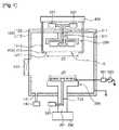
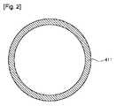
図1は本発明の第1実施形態による基板処理装置を示す模式図であり、図2及び図3は本発明の第1実施形態による支持台の支持部を示す底面図である。FIG. 1 is a schematic view showing a substrate processing apparatus according to a first embodiment of the present invention, and FIGS. 2 and 3 are bottom views showing a support portion of a support base according to the first embodiment of the present invention.
図1を参照すると、本実施形態による基板処理装置は反応空間を提供するチャンバ100と、前記チャンバ100内部の下部に設けられるステージ200と、前記ステージ200に対向して前記チャンバ100内部の上部に設けられるプラズマ遮蔽部300と、前記ステージ200と前記プラズマ遮蔽部300との間に基板10を支持する支持台410と、前記ステージ200と前記ステージ200と前記プラズマ遮蔽部300との間にプラズマを形成するためのプラズマ発生手段510、520、530と、を含む。ここで、基板10はプラズマ処理、例えば、エッチング、蒸着、洗浄などが要求される板状の被処理体、例えば、ウェーハ、ガラスパネルなどを通称する意味で使われる。Referring to FIG. 1, the substrate processing apparatus according to the present embodiment includes a
チャンバ100は、内部に所定空間を備えるチャンバ本体110と、チャンバ本体110を覆うチャンバリッド120を備える。この時、前記チャンバリッド120は、前記チャンバ本体110の上部と気密するように接続され、チャンバ100内部に密閉された反応空間を形成する。もちろん、チャンバ本体110とチャンバリッド120は一体的に形成できる。このようなチャンバ100には基板10の搬入又は搬出のための開閉手段と、残留ガスの排気のための排気手段が備えられる。例えば、本実施形態はチャンバ100の側壁にゲート130を形成して前記開閉手段を構成し、チャンバ100の下壁に排気口141及び前記排気口141に排気ポンプ140を連結して前記排気手段を構成する。一方、前記のチャンバ100は接地電源に連結されてチャンバ100を通して電流が流れないように構成することが望ましい。The
ステージ200は本体部の上部中央に突出部が備えられる。前記突出部は基板10のエッジエッチングの際に基板10背面の中央部を配置する配置領域を提供する。また、前記ステージ200は基板10の背面に反応ガス又は非反応ガスを供給する第1供給口210を備え、前記第1供給口210の一側はチャンバ100外側に延長されて第1ガス供給部220と連通される。この時、チャンバ100外側から供給された反応ガス又は非反応ガスが基板10背面に噴射される前に複数の流れに分割されるように第1供給口210の基板噴射方向の他端、即ち、基板に向けられた端部は複数の開口で形成される。これにより、基板10の背面領域に均一なガス供給が可能である。また、前記ステージ200は駆動手段によって昇降運動及び回転運動ができるように設けられることが望ましい。本実施形態はステージ200の本体部の下部が駆動側231の一端に結合され、前記駆動側231の他端はチャンバ100の下壁を貫通して前記駆動側231に昇降力及び回転力を印加する第1駆動部230に結合される。The
一方、図示してないが、前記ステージ200の突出部には基板10を固定するためのチャック手段、例えば、機械力、静電力、真空吸入力などを利用するチャック部材を備え、前記ステージ200の本体部にはチャンバ100内部の工程温度を一定に維持させるための冷却手段、例えば、冷却管及び前記冷却管を循環する冷媒材を備え、又は加熱手段、例えば、電気発熱ヒーター、ランプヒーターなどを備えることができる。On the other hand, although not shown, the projecting portion of the
プラズマ遮蔽部300は本体の下部中央に突出部が備えられる。前記突出部は基板10の背面エッチングの際、基板10前面の中央領域に接するように配置されて基板10前面の中央領域にプラズマが流入されることを防止する役割だけではなく、局所的なプラズマ発生を誘導できる。また、前記プラズマ遮蔽部300は基板10前面のエッジ領域に反応ガスを供給する第2供給口311及び基板10前面の中央領域に非反応ガスを供給する第3供給口312を備える。前記第2供給口311の一側はチャンバ100外側に延長されて第2ガス供給部321と連通され、前記第3供給部312の一側はチャンバ100外側に延長されて第3ガス供給部322と連通される。この時、チャンバ100外側から供給されたガスが基板方向に噴射される前に複数の流れに分割されるように第2及び第3供給口311、312の基板噴射方向の他端、即ち、基板に向けられた端部は複数の開口で形成される。これにより、基板10前面のエッジ領域又は中央領域に均一なガス供給が可能である。The
一方、前記ステージ200と前記プラズマ遮蔽部300の突出部は基板10と同じ形に製作されることが望ましく、基板10の大きさよりすこし小さく製作されることが望ましいが、その大きさは工程によって変更可能である。これにより、前記ステージ200の突出部の上に、基板10の背面を配置するか、前記プラズマ遮蔽部300の突出部を基板10の前面に接近しても、基板10のエッジ領域が露出されて基板10のエッジ領域にプラズマが自由に流入できるので、基板10のエッジエッチングを容易に行える。この時、露出する基板10のエッジ領域は、基板10の端部でおおよそ0.1ないし5mmであることが望ましい。また、前記ステージ200の突出部は、その上部の少なくとも一部が支持台410の内側の空間に挿入できるように、その平面直径d2が支持台410の内側の直径d1より小さく製作されることが望ましい。これにより、第1駆動部230を動作させてステージ200を上昇させると、支持台410に支持された基板10がステージ200の突出部の上に配置されて一緒に上昇することによって、基板10がプラズマ遮蔽部300に近接できる。Meanwhile, the protrusions of the
支持台410はステージ200とプラズマ遮蔽部300の間の空間で基板10を支持し、前記基板10を上下に移動させて基板10とステージ200の間の間隔及び基板10とプラズマ遮蔽部300の間の間隔を調節する。このような支持台410はチャンバ100の上部に設けられ、上部から下部に伸縮されるアーム部413及び前記アーム部413の端部で内側に折り曲げられて上面に基板10のエッジ領域が支持される支持部411を含む。The support table 410 supports the
前記アーム部413は内側に基板10を配置することができ、基板10の荷重を安定的に支持できる構造、例えば、一対の長い棒状又は筒状に製作されることが望ましい。このようなアーム部413の一端は、チャンバ100外側に備えられる第2駆動部420と連結されて上下に伸縮可能に構成され、前記第2駆動部420によって前記アーム部413の他端がステージ200とプラズマ遮蔽部300の間で上下に移動可能に構成される。前記支持部411は基板10と同じ形に製作され、その上面が基板10のエッジ領域を安定的に支持できる構造、例えば、基板10が円形であれば、図2に示されるように単一のリング状、又は図3に示されるように単一のリングが複数に分割された分割片の形に製作されることが望ましい。この時、リング状の内周直径d1は基板10の大きさよりすこし小さく製作されることが望ましい。従って、基板10背面はエッジ領域を除いての大部分の中央領域を露出できる。また、前記支持部411と前記アーム部413の間に形成される折曲部412は内側で平らに、又は外側から内側に下向きに傾斜を持つように形成されることが望ましい。これにより、基板10が平面に安定的に配置されるか、又は傾斜に沿って案内されながら支持部411上に自動整列される効果を得ることができる。一方、前記の支持台410は、基板処理装置のその他の構成によって電気的に干渉されないように浮遊(floating)状態で構成されるのが望ましく、このためAl2O3のような絶縁物質に形成されることが望ましい。The
プラズマ発生手段は、基板10のプラズマ処理のためにステージ200とプラズマ遮蔽部300の間にプラズマを形成する役割をする。本実施形態はステージ200が下部電極として機能し、プラズマ遮蔽部300が上部電極として機能するように構成される。この時、プラズマ遮蔽部300は接地電源に接続され、ステージ200は電源供給部530に接続されてプラズマ電源が印加される。本実施形態では、電源供給部530はステージ200に高周波(Radio Frequency)電源を供給し、インピーダンス整合部531は高周波電源の最大パワー(power)とステージ200の負荷(load)の間のインピーダンス(impedance)を整合(matching)する。もちろん、前記プラズマ発生手段は、これに限定されるのではなく、ステージ200とプラズマ遮蔽部300の間にプラズマを形成できれば、どんな手段でも変更可能である。例えば、プラズマ発生のための電極はアンテナの形態でチャンバ100外側に設けられることができ、高周波電源の代わりに直流DC電源を使うこともできる。また、ステージ200に接地電源を印加し、プラズマ遮蔽部300に高周波電源を印加することもできる。The plasma generating unit serves to form plasma between the
一方、このような構成の本実施形態による基板処理装置は、基板のエッジ領域だけではなく、背面領域にプラズマ処理を単一チャンバ内で個別的に行うことができ、これを次のようにより詳しく説明する。On the other hand, the substrate processing apparatus according to the present embodiment having such a configuration can perform plasma processing individually in a single chamber not only in the edge region of the substrate but also in the back surface region. explain.
図4は本発明の第1実施形態によるプラズマ処理動作を説明するための工程フローチャートであり、図5は本発明の第1実施形態による第1プラズマ処理動作を説明するためのチャンバ模式図であり、図6は本発明の第1実施形態による第2プラズマ処理動作を説明するためのチャンバ模式図である。FIG. 4 is a process flowchart for explaining the plasma processing operation according to the first embodiment of the present invention, and FIG. 5 is a schematic chamber diagram for explaining the first plasma processing operation according to the first embodiment of the present invention. FIG. 6 is a schematic view of the chamber for explaining the second plasma processing operation according to the first embodiment of the present invention.
図4及び図5を参照すると、第1プラズマ処理動作では基板10のエッジ領域にプラズマ処理を行う。まず、所定の薄膜が形成された基板10をチャンバ100内部に搬入させて支持台410に支持する。引き続き、ステージ200を上昇させてステージ200の突出部の上に基板10の背面を配置した後、ステージ200をもっと上昇させて基板10前面の中央領域とプラズマ遮蔽部300の間をプラズマが非活性化される第1間隔、即ち、0.1ないし0.7mmの範囲に調節する(S110)。引き続き、プラズマ遮蔽部300の第2供給口311を通して基板100前面のエッジ領域に反応ガスを供給し、第3供給口312を通して基板100前面の中央領域に非反応ガスを供給する(S120)。その後、ステージ200にプラズマ電源を印加すると、プラズマが形成されて基板10表面にプラズマ処理が実施される(S130)。この時、基板10背面の中央領域はステージ200の突出部の上に配置されて密閉され、基板10前面の中央領域には第3供給口311を通して供給される非反応ガスによって一種の遮断膜が形成される。従って、前記の第1プラズマ処理動作では基板10前面の中央領域及び基板背面の中央領域が保護されながら、露出した基板のエッジ領域だけがプラズマ処理される。Referring to FIGS. 4 and 5, in the first plasma processing operation, plasma processing is performed on the edge region of the
図4及び図6を参照すると、第2プラズマ処理動作では基板10の背面領域にプラズマ処理を行う。前記の第1プラズマ処理動作が終われば、ステージ200を下降させて基板10とプラズマ遮蔽部300の間を離隔させる。これによって、基板10は支持台410の上に支持される。引き続き、支持台410を上昇させて基板10前面の中央領域とプラズマ遮蔽部300の間をプラズマが非活性化される第2間隔、即ち、0.1ないし0.7mmの範囲に調節する(S140)。引き続き、ステージ200の第1供給口210を通して基板10背面に反応ガスを供給して(S150)、ステージ200にプラズマ電源を印加すると、プラズマが形成されて基板10背面にプラズマ処理が実施される(S160)。この時、基板10の前面領域はプラズマ遮蔽部300に近接されてプラズマ露出が防止される。従って、前記の第2プラズマ処理動作では基板10の前面が保護されながら基板10の背面領域だけがプラズマ処理される。Referring to FIGS. 4 and 6, in the second plasma processing operation, plasma processing is performed on the back surface region of the
一方、前記第1及び第2プラズマ処理過程で反応ガスはCF4、CHF4、SF6、C2F6、C4F8又はNF3のようなフッ素ラジカル、BCl3又はCl2のような塩素ラジカルの少なくとも一つを含むことが望ましい。そのほかの基板10に堆積された薄膜やパーティクルなどを化学的にエッチングできる多様なエッチングガスを含むことができる。また、非反応ガスは酸素、水素、窒素及び不活性ガスを含むことができ、そのほかの基板10に形成された薄膜を保護できる多様な保護ガスを含むことができる。もちろん、工程によって前記反応、非反応ガスを混合して使うこともできる。Meanwhile, in the first and second plasma treatment processes, the reactive gas is a fluorine radical such as CF4 , CHF4 , SF6 , C2 F6 , C4 F8 or NF3 , such as BCl3 or Cl2 . It is desirable to include at least one of chlorine radicals. Various etching gases capable of chemically etching thin films and particles deposited on
<第2実施形態>Second Embodiment
一方、前述の基板処理装置は前述の構成に限定されることではなく、多様な実施形態が可能である。下記では、このような可能性の一例として本発明の第2実施形態による基板処理装置について説明する。この時、前述の実施形態と重複される説明は省略して簡単に説明する。On the other hand, the above-described substrate processing apparatus is not limited to the above-described configuration, and various embodiments are possible. In the following, a substrate processing apparatus according to a second embodiment of the present invention will be described as an example of such a possibility. At this time, the description which overlaps with the above-mentioned embodiment is omitted, and it demonstrates simply.
図7は本発明の第2実施形態による基板処理装置を示す模式図である。FIG. 7 is a schematic view showing a substrate processing apparatus according to the second embodiment of the present invention.
図7を参照すると、本実施形態による基板処理装置は反応空間を提供するチャンバ100と、前記チャンバ100内部の下部に設けられるステージ200と、前記ステージ200に対向して前記チャンバ100内部の上部に設けられるプラズマ遮蔽部600と、前記ステージ200と前記プラズマ遮蔽部600の間に基板10を支持する支持台710と、前記ステージ200と前記プラズマ遮蔽部600の間にプラズマを形成するためのプラズマ発生手段810、820と、を含む。Referring to FIG. 7, the substrate processing apparatus according to the present embodiment includes a
前述の第1実施形態とは違い、前記支持台710はチャンバ100の下部に設けられ、前記プラズマ遮蔽部600は駆動手段によって昇降運動及び回転運動ができるように設けられる。即ち、支持台710はチャンバ100の下部に設けられて下部から上部に伸縮されるアーム部713と、前記アーム部713の後端で内側に折り曲げられて上面に基板10のエッジ領域が支持される支持部711と、を備え、支持部711とアーム部713の間の折曲部713には基板を配置するために平らな面、又は基板整列のための傾斜面を持つように形成される。このようなアーム部713の一端はチャンバ100外側に備えられる第2駆動部720と連結されて上下に伸縮可能に構成され、前記第2駆動部720によって前記アーム部713の他端がステージ200とプラズマ遮蔽部600の間で上下に移動可能に構成される。また、プラズマ遮蔽部600の本体部の上部は駆動側611の一端に結合され、前記駆動側611の他端はチャンバ100の上壁を貫通して前記駆動側611に昇降力及び回転力を印加する第3駆動部610に結合される。これにより、ステージ200と基板10、又は基板10とプラズマ遮蔽部600の間の間隔は支持台710の昇降だけではなく、ステージ200又はプラズマ遮蔽部600の昇降によっても自由に調節できるので、工程条件をより容易に調節できる。Unlike the first embodiment described above, the support base 710 is provided in the lower part of the
プラズマ発生手段810、820は支持台710の外側領域に備えられるプラズマ電極810と、前記プラズマ電極にプラズマ電源を供給する電源供給部820と、を含む。本実施形態の電源供給部820はプラズマ電極810に高周波電源を供給し、インピーダンス整合部821は高周波電源の最大パワーとプラズマ電極810の負荷の間のインピーダンスを整合する。一方、前記プラズマ電極810は基板10の形に対応して平板、又はリング状に製作され、基板10のエッジ領域により高密度の分布を持つプラズマを発生できるので、基板10のエッジ領域にプラズマ処理をより効果的に行うことができる。The plasma generating means 810 and 820 include a
一方、前述の第1及び第2実施形態では薄膜エッチングのためにプラズマを利用する基板処理装置について説明したが、本発明はこれに限定されることなく、本発明による基板処理装置はプラズマを利用する多様な工程、例えば、薄膜蒸着、薄膜洗浄などにも使われることができる。Meanwhile, in the first and second embodiments described above, the substrate processing apparatus using plasma for thin film etching has been described. However, the present invention is not limited to this, and the substrate processing apparatus according to the present invention uses plasma. It can also be used for various processes such as thin film deposition and thin film cleaning.
以上、本発明について実施形態及び添付された図面に基づいて説明したが、本発明はこれに限定されるものではなく、後述される特許請求範囲によって限定される。従って、本技術分野の通常の知識を持った者なら、後述される特許請求範囲の技術的思想の範囲内で、本発明が多様に変形及び修正できると理解できるはずである。As mentioned above, although this invention was demonstrated based on embodiment and attached drawing, this invention is not limited to this, It is limited by the claim mentioned later. Therefore, it should be understood by those skilled in the art that the present invention can be variously modified and modified within the scope of the technical idea of the claims described later.
本発明では、プラズマ処理は単一チャンバ内で基板のエッジ領域及び背面領域のそれぞれで個別的に行っている。よって、装置の設置空間が減り、生産ラインの空間活用性を高めることができる。更にチャンバ間で基板の移動による雰囲気への基板の露出がないので、基板汚染が少ない。またチャンバ間の基板の移動による待機時間がないので、全体の処理時間を減少できる。In the present invention, plasma processing is performed individually in the edge region and the back region of the substrate in a single chamber. Therefore, the installation space for the apparatus is reduced, and the space utilization of the production line can be improved. Further, since the substrate is not exposed to the atmosphere due to the movement of the substrate between the chambers, there is little substrate contamination. In addition, since there is no waiting time due to the movement of the substrate between the chambers, the entire processing time can be reduced.
Claims (16)
Translated fromJapanese前記チャンバ内部に設けられるステージと、
前記ステージに対向して前記チャンバ内部に設けられるプラズマ遮蔽部と、
前記ステージと前記プラズマ遮蔽部との間に基板を支持する支持台と、
前記ステージに備えられ、前記基板の一面に反応ガス又は非反応ガスを供給する第1供給口と、
前記プラズマ遮蔽部に備えられ、前記基板の他面に反応ガスを供給する第2供給口及び非反応ガスを供給する第3供給口と、を含み、
前記支持台は、他の構成物に対して電気的に干渉しないように構成され、
前記支持台は、前記チャンバ内部で伸縮自在のアーム部と、前記アーム部の端部で内側に折り曲げられて上面に前記基板のエッジ領域が支持される支持部とを備え、前記支持部は傾斜をもつように形成される基板処理装置。A chamber providing a reaction space;
A stage provided inside the chamber;
A plasma shield provided inside the chamber facing the stage;
A support for supporting the substrate between the stage and the plasma shielding unit;
A first supply port provided in the stage for supplying a reactive gas or a non-reactive gas to one surface of the substrate;
A second supply port for supplying a reactive gas to the other surface of the substrate; and a third supply port for supplying a non-reactive gas.
The support base is configured not to electrically interfere with other components,
The support base includesan arm portion that can be expanded and contracted inside the chamber , and a supportportion that is bent inward at an end portion of the arm portion to support an edge region of the substrateon an upper surface,and the support portion is inclined. A substrate processing apparatus formed to have
前記ステージを上昇させて、前記ステージの上に基板を配置した状態で、前記基板と前記プラズマ遮蔽部との間を第1間隔に調節する段階と、
前記プラズマ遮蔽部を通して前記基板のエッジ領域に反応ガスを供給し、プラズマを形成して、前記基板のエッジ領域をプラズマ処理する第1プラズマ処理を行う段階と、
前記ステージを下降させて前記基板を前記支持台の上に支持して、前記ステージと前記基板を離隔させた状態で、前記基板と前記プラズマ遮蔽部の間を第2間隔に調節する段階と、
前記ステージを通して前記基板の背面の中央領域を含む背面領域に反応ガスを供給し、プラズマを形成して、前記基板の前記背面領域をプラズマ処理する第2プラズマ処理を行う段階と、を含み、
上記の過程は単一チャンバー内で行われる基板処理方法。The substrate is supported on the support portion of the support table including an arm portion that is expanded and contracted inside the chamber, and a support portion that is bent inward at an end portion of the arm portion and an edge region of the substrate is supported on the upper surface, Placing the substrate between the stage and the plasma shield;
Is raised the stage, in the state in which the substrate on the stage, and adjusting between the substrate and the plasma shielding member in a first interval,
Supplying a reactive gas to the edge region of the substrate through the plasma shield, forming a plasma, and performing a first plasma process for plasma processing the edge region of the substrate;
Lowering the stage and supporting the substrate on the support, and adjusting the second interval between the substrate and the plasma shielding unit in a state where the stage and the substrate are separated from each other;
Supplying a reactive gas to the back regionincluding a central region of the back surface of the substrate through the stage, to form a plasma, it comprises the steps of performing a second plasma treatment using a plasma treatmentthe rear region of the substrate,
The above process is a substrate processing method performed in a single chamber.
前記プラズマ遮蔽部を通して前記基板の中央領域に非反応ガスを供給しながら行う請求項9記載の基板処理方法。Performing the first plasma treatment comprises:
The substrate processing method according to claim9, wherein the non-reactive gas is supplied to the central region of the substrate through the plasma shielding portion.
Applications Claiming Priority (3)
| Application Number | Priority Date | Filing Date | Title |
|---|---|---|---|
| KR1020070141363AKR101432562B1 (en) | 2007-12-31 | 2007-12-31 | Substrate processing apparatus and substrate processing method |
| KR10-2007-0141363 | 2007-12-31 | ||
| PCT/KR2008/007291WO2009084823A1 (en) | 2007-12-31 | 2008-12-10 | Apparatus and method for processing substrate |
Publications (2)
| Publication Number | Publication Date |
|---|---|
| JP2011512021A JP2011512021A (en) | 2011-04-14 |
| JP5597891B2true JP5597891B2 (en) | 2014-10-01 |
Family
ID=40824504
Family Applications (1)
| Application Number | Title | Priority Date | Filing Date |
|---|---|---|---|
| JP2010540561AExpired - Fee RelatedJP5597891B2 (en) | 2007-12-31 | 2008-12-10 | Substrate processing apparatus and substrate processing method |
Country Status (6)
| Country | Link |
|---|---|
| US (1) | US8864936B2 (en) |
| JP (1) | JP5597891B2 (en) |
| KR (1) | KR101432562B1 (en) |
| CN (1) | CN101911251B (en) |
| TW (1) | TWI460805B (en) |
| WO (1) | WO2009084823A1 (en) |
Families Citing this family (21)
| Publication number | Priority date | Publication date | Assignee | Title |
|---|---|---|---|---|
| EP2551240B1 (en)* | 2008-05-21 | 2020-11-11 | Basf Se | Cu containing zeolites having CHA structure |
| US9695502B2 (en) | 2012-03-30 | 2017-07-04 | Applied Materials, Inc. | Process kit with plasma-limiting gap |
| US9388494B2 (en)* | 2012-06-25 | 2016-07-12 | Novellus Systems, Inc. | Suppression of parasitic deposition in a substrate processing system by suppressing precursor flow and plasma outside of substrate region |
| US9399228B2 (en) | 2013-02-06 | 2016-07-26 | Novellus Systems, Inc. | Method and apparatus for purging and plasma suppression in a process chamber |
| US20140225502A1 (en)* | 2013-02-08 | 2014-08-14 | Korea Institute Of Machinery & Materials | Remote plasma generation apparatus |
| US9633824B2 (en) | 2013-03-05 | 2017-04-25 | Applied Materials, Inc. | Target for PVD sputtering system |
| US9355876B2 (en)* | 2013-03-15 | 2016-05-31 | Applied Materials, Inc. | Process load lock apparatus, lift assemblies, electronic device processing systems, and methods of processing substrates in load lock locations |
| JP6178488B2 (en)* | 2013-03-15 | 2017-08-09 | アプライド マテリアルズ インコーポレイテッドApplied Materials,Incorporated | Processing system, apparatus and method adapted for substrate processing in electronic device manufacturing |
| KR101568273B1 (en)* | 2013-12-27 | 2015-11-19 | 엘지디스플레이 주식회사 | Apparatus for processing flexible substrate and method of processing flexible substrate using the same |
| JP5837962B1 (en)* | 2014-07-08 | 2015-12-24 | 株式会社日立国際電気 | Substrate processing apparatus, semiconductor device manufacturing method, and gas rectifier |
| US9633862B2 (en)* | 2015-08-31 | 2017-04-25 | Kabushiki Kaisha Toshiba | Semiconductor manufacturing apparatus and semiconductor manufacturing method |
| US10403515B2 (en)* | 2015-09-24 | 2019-09-03 | Applied Materials, Inc. | Loadlock integrated bevel etcher system |
| US9758868B1 (en) | 2016-03-10 | 2017-09-12 | Lam Research Corporation | Plasma suppression behind a showerhead through the use of increased pressure |
| US10403474B2 (en)* | 2016-07-11 | 2019-09-03 | Lam Research Corporation | Collar, conical showerheads and/or top plates for reducing recirculation in a substrate processing system |
| KR102528559B1 (en)* | 2016-07-26 | 2023-05-04 | 삼성전자주식회사 | Apparatus for manufacturing a large size substrate |
| TWI656235B (en)* | 2017-07-28 | 2019-04-11 | 漢民科技股份有限公司 | Chemical vapor deposition system |
| KR102225958B1 (en)* | 2019-06-05 | 2021-03-11 | 세메스 주식회사 | A Substrate processing apparatus and method |
| KR102214333B1 (en) | 2019-06-27 | 2021-02-10 | 세메스 주식회사 | Apparatus and method for treating substrate |
| US12087573B2 (en) | 2019-07-17 | 2024-09-10 | Lam Research Corporation | Modulation of oxidation profile for substrate processing |
| US20230314954A1 (en)* | 2020-06-22 | 2023-10-05 | Lam Research Corporation | Dry backside and bevel edge clean of photoresist |
| US20250037974A1 (en)* | 2023-07-27 | 2025-01-30 | Applied Materials, Inc. | Chamber for substrate backside and bevel deposition |
Family Cites Families (12)
| Publication number | Priority date | Publication date | Assignee | Title |
|---|---|---|---|---|
| US6159299A (en)* | 1999-02-09 | 2000-12-12 | Applied Materials, Inc. | Wafer pedestal with a purge ring |
| CN101038863B (en)* | 2001-02-15 | 2011-07-06 | 东京毅力科创株式会社 | Method and apparatus for processing workpiece |
| US6586886B1 (en)* | 2001-12-19 | 2003-07-01 | Applied Materials, Inc. | Gas distribution plate electrode for a plasma reactor |
| JP2003193229A (en)* | 2001-12-21 | 2003-07-09 | Toshiba Corp | Piezoelectric substrate film forming apparatus and film forming method |
| JP2004022821A (en)* | 2002-06-17 | 2004-01-22 | Shibaura Mechatronics Corp | Dry etching method and apparatus |
| CN100397589C (en)* | 2003-05-12 | 2008-06-25 | 索绍株式会社 | Plasma etching chamber and plasma etching system using same |
| JP2006165093A (en)* | 2004-12-03 | 2006-06-22 | Tokyo Electron Ltd | Plasma processing device |
| US20060237138A1 (en)* | 2005-04-26 | 2006-10-26 | Micron Technology, Inc. | Apparatuses and methods for supporting microelectronic devices during plasma-based fabrication processes |
| JP2006319043A (en)* | 2005-05-11 | 2006-11-24 | Hitachi High-Technologies Corp | Plasma processing equipment |
| JP4705816B2 (en)* | 2005-07-27 | 2011-06-22 | 株式会社日立ハイテクノロジーズ | Plasma processing equipment |
| KR101218114B1 (en)* | 2005-08-04 | 2013-01-18 | 주성엔지니어링(주) | Etching apparatus using the plasma |
| KR20070034811A (en)* | 2005-09-26 | 2007-03-29 | 삼성전자주식회사 | Substrate Processing Apparatus and Method |
- 2007
- 2007-12-31KRKR1020070141363Apatent/KR101432562B1/ennot_activeExpired - Fee Related
- 2008
- 2008-12-10WOPCT/KR2008/007291patent/WO2009084823A1/enactiveApplication Filing
- 2008-12-10CNCN2008801234343Apatent/CN101911251B/ennot_activeExpired - Fee Related
- 2008-12-10USUS12/810,915patent/US8864936B2/enactiveActive
- 2008-12-10JPJP2010540561Apatent/JP5597891B2/ennot_activeExpired - Fee Related
- 2008-12-29TWTW097151219Apatent/TWI460805B/ennot_activeIP Right Cessation
Also Published As
| Publication number | Publication date |
|---|---|
| TW200943455A (en) | 2009-10-16 |
| US20100288728A1 (en) | 2010-11-18 |
| CN101911251A (en) | 2010-12-08 |
| KR20090073425A (en) | 2009-07-03 |
| WO2009084823A1 (en) | 2009-07-09 |
| KR101432562B1 (en) | 2014-08-21 |
| TWI460805B (en) | 2014-11-11 |
| JP2011512021A (en) | 2011-04-14 |
| CN101911251B (en) | 2012-03-28 |
| US8864936B2 (en) | 2014-10-21 |
Similar Documents
| Publication | Publication Date | Title |
|---|---|---|
| JP5597891B2 (en) | Substrate processing apparatus and substrate processing method | |
| TWI633573B (en) | Plasma processing device and method | |
| KR20220036933A (en) | Systems and methods for in-situ wafer edge and backside plasma cleaning | |
| TWI840355B (en) | Cleaning method and substrate processing apparatus | |
| KR101050641B1 (en) | Substrate Processing Unit and Shower Head | |
| JP4970434B2 (en) | Plasma reactor and method of using plasma reactor | |
| JP4757856B2 (en) | Plasma processing equipment | |
| TWI725034B (en) | Plasma processing method | |
| KR101985601B1 (en) | Plasma Processing Apparatus | |
| KR100900703B1 (en) | Plasma treatment apparatus and plasma treatment method | |
| JP2007220926A (en) | Apparatus and method for plasma treatment | |
| KR100777466B1 (en) | Plasma etching device for simultaneously etching the edge and back of the substrate to be processed and substrate lifting device therefor | |
| WO2021250981A1 (en) | Plasma processing apparatus and plasma processing method | |
| JP6807558B2 (en) | Plasma processing method and plasma processing equipment | |
| CN114068279A (en) | Stage and Plasma Processing Device | |
| KR101517720B1 (en) | Electrostatic chuck and plasma generation apparatus using the same | |
| CN117637431B (en) | Cleaning method and plasma treatment device | |
| KR101390785B1 (en) | Apparatus for processing substrate and method for processing substrate | |
| JP2019046865A (en) | Plasma processing apparatus and method | |
| JP2022104964A (en) | Shadow frame with sides with different profiles to improve sedimentation uniformity | |
| KR20090057840A (en) | Plasma treatment apparatus and plasma treatment method | |
| TW201426897A (en) | Deposition shield for plasma enhanced substrate processing | |
| KR20150034435A (en) | Substrate processing apparatus | |
| KR101418368B1 (en) | Substrate supporting apparatus and substrate edge etching apparatus having the same | |
| KR20090106258A (en) | Plasma processing apparatus and plasma processing method |
Legal Events
| Date | Code | Title | Description |
|---|---|---|---|
| A621 | Written request for application examination | Free format text:JAPANESE INTERMEDIATE CODE: A621 Effective date:20111209 | |
| A977 | Report on retrieval | Free format text:JAPANESE INTERMEDIATE CODE: A971007 Effective date:20120927 | |
| A131 | Notification of reasons for refusal | Free format text:JAPANESE INTERMEDIATE CODE: A131 Effective date:20121002 | |
| A521 | Request for written amendment filed | Free format text:JAPANESE INTERMEDIATE CODE: A523 Effective date:20121207 | |
| A131 | Notification of reasons for refusal | Free format text:JAPANESE INTERMEDIATE CODE: A131 Effective date:20131001 | |
| A521 | Request for written amendment filed | Free format text:JAPANESE INTERMEDIATE CODE: A523 Effective date:20131213 | |
| TRDD | Decision of grant or rejection written | ||
| A01 | Written decision to grant a patent or to grant a registration (utility model) | Free format text:JAPANESE INTERMEDIATE CODE: A01 Effective date:20140701 | |
| A711 | Notification of change in applicant | Free format text:JAPANESE INTERMEDIATE CODE: A711 Effective date:20140722 | |
| A61 | First payment of annual fees (during grant procedure) | Free format text:JAPANESE INTERMEDIATE CODE: A61 Effective date:20140725 | |
| A521 | Request for written amendment filed | Free format text:JAPANESE INTERMEDIATE CODE: A821 Effective date:20140722 | |
| R150 | Certificate of patent or registration of utility model | Ref document number:5597891 Country of ref document:JP Free format text:JAPANESE INTERMEDIATE CODE: R150 | |
| R250 | Receipt of annual fees | Free format text:JAPANESE INTERMEDIATE CODE: R250 | |
| R250 | Receipt of annual fees | Free format text:JAPANESE INTERMEDIATE CODE: R250 | |
| R250 | Receipt of annual fees | Free format text:JAPANESE INTERMEDIATE CODE: R250 | |
| LAPS | Cancellation because of no payment of annual fees |