JP5597583B2 - Touch panel device and electronic device - Google Patents
Touch panel device and electronic deviceDownload PDFInfo
- Publication number
- JP5597583B2 JP5597583B2JP2011071250AJP2011071250AJP5597583B2JP 5597583 B2JP5597583 B2JP 5597583B2JP 2011071250 AJP2011071250 AJP 2011071250AJP 2011071250 AJP2011071250 AJP 2011071250AJP 5597583 B2JP5597583 B2JP 5597583B2
- Authority
- JP
- Japan
- Prior art keywords
- touch panel
- vibration element
- piezoelectric vibration
- glass substrate
- panel device
- Prior art date
- Legal status (The legal status is an assumption and is not a legal conclusion. Google has not performed a legal analysis and makes no representation as to the accuracy of the status listed.)
- Active
Links
Images


Classifications
- G—PHYSICS
- G06—COMPUTING OR CALCULATING; COUNTING
- G06F—ELECTRIC DIGITAL DATA PROCESSING
- G06F1/00—Details not covered by groups G06F3/00 - G06F13/00 and G06F21/00
- G06F1/16—Constructional details or arrangements
- G06F1/1613—Constructional details or arrangements for portable computers
- G06F1/1626—Constructional details or arrangements for portable computers with a single-body enclosure integrating a flat display, e.g. Personal Digital Assistants [PDAs]
- G—PHYSICS
- G06—COMPUTING OR CALCULATING; COUNTING
- G06F—ELECTRIC DIGITAL DATA PROCESSING
- G06F3/00—Input arrangements for transferring data to be processed into a form capable of being handled by the computer; Output arrangements for transferring data from processing unit to output unit, e.g. interface arrangements
- G06F3/01—Input arrangements or combined input and output arrangements for interaction between user and computer
- G06F3/03—Arrangements for converting the position or the displacement of a member into a coded form
- G06F3/041—Digitisers, e.g. for touch screens or touch pads, characterised by the transducing means
- G—PHYSICS
- G06—COMPUTING OR CALCULATING; COUNTING
- G06F—ELECTRIC DIGITAL DATA PROCESSING
- G06F1/00—Details not covered by groups G06F3/00 - G06F13/00 and G06F21/00
- G06F1/16—Constructional details or arrangements
- G06F1/1613—Constructional details or arrangements for portable computers
- G06F1/1633—Constructional details or arrangements of portable computers not specific to the type of enclosures covered by groups G06F1/1615 - G06F1/1626
- G06F1/1637—Details related to the display arrangement, including those related to the mounting of the display in the housing
- G06F1/1643—Details related to the display arrangement, including those related to the mounting of the display in the housing the display being associated to a digitizer, e.g. laptops that can be used as penpads
- G—PHYSICS
- G06—COMPUTING OR CALCULATING; COUNTING
- G06F—ELECTRIC DIGITAL DATA PROCESSING
- G06F3/00—Input arrangements for transferring data to be processed into a form capable of being handled by the computer; Output arrangements for transferring data from processing unit to output unit, e.g. interface arrangements
- G06F3/01—Input arrangements or combined input and output arrangements for interaction between user and computer
- G06F3/016—Input arrangements with force or tactile feedback as computer generated output to the user
Landscapes
- Engineering & Computer Science (AREA)
- General Engineering & Computer Science (AREA)
- Theoretical Computer Science (AREA)
- Human Computer Interaction (AREA)
- Physics & Mathematics (AREA)
- General Physics & Mathematics (AREA)
- Computer Hardware Design (AREA)
- Position Input By Displaying (AREA)
- User Interface Of Digital Computer (AREA)
Description
Translated fromJapanese本発明は、タッチパネル装置及び電子機器に関し、更に具体的には、圧電振動素子を用いたフォースフィードバック機能(ないしハプティック機能)を備えたタッチパネル装置及びそれを備えた電子機器に関するものである。 The present invention relates to a touch panel device and an electronic device, and more specifically to a touch panel device having a force feedback function (or haptic function) using a piezoelectric vibration element and an electronic device including the touch panel device.
携帯電話等に用いられる液晶パネルなどの表示装置に、入力装置として感圧式や静電容量式のタッチパネルが用いられるが、通常の機械式スイッチと異なり、押下したときの沈み込み深さが小さいため、押したのかどうかを指先等で感知することが難しい。そのため、押下に合わせて振動等の機械的な動きを発生させ、触覚的に押下を感知せしめるハプティック機能を備えたタッチパネル装置が開発されている。 A pressure-sensitive or capacitive touch panel is used as an input device for a display device such as a liquid crystal panel used in a mobile phone or the like, but unlike a normal mechanical switch, the depth of depression when pressed is small. It is difficult to detect with the fingertip or not. For this reason, a touch panel device having a haptic function that generates a mechanical movement such as vibration in response to the pressing and senses the pressing tactilely has been developed.
ハプティック機能を実現させるための駆動源としては、例えば、下記特許文献1の振動素子を有するパネル部材に示すような圧電アクチュエータや、下記特許文献2のハプティックパネル装置に示すような電磁式のアクチュエータが用いられる。また、表示用パネルへのアクチュエータの取り付けに関しては、例えば、下記特許文献3の触覚提示機能付き表示装置に示される液晶,タッチパネル,ハプティックパネルを積層した構造や、下記特許文献4の携帯型電子デバイスおよび制御方法に示される液晶の下側からユニットを駆動するblackberryタイプのように、液晶パネルの下側にアクチュエータを配置する例がある。このような配置により、表示装置の画像が遮られることなく、振動を指先に伝達することができる。また、前記特許文献1や特許文献2に示す技術のように、駆動源となるアクチュエータを、パネル面内の表示されない周囲部分に配置することで、視覚的な表示と触覚による呈示を両立させる例もある。 As a driving source for realizing the haptic function, for example, a piezoelectric actuator as shown in a panel member having a vibration element of Patent Document 1 below, or an electromagnetic actuator as shown in a haptic panel device of Patent Document 2 below. Used. Regarding the attachment of the actuator to the display panel, for example, a structure in which a liquid crystal, a touch panel, and a haptic panel are stacked as shown in the display device with a tactile presentation function of Patent Document 3 below, or a portable electronic device of Patent Document 4 below. In addition, there is an example in which an actuator is arranged on the lower side of the liquid crystal panel as in the blackberry type in which the unit is driven from the lower side of the liquid crystal shown in the control method. With such an arrangement, vibrations can be transmitted to the fingertip without blocking the image of the display device. In addition, as in the techniques shown in Patent Document 1 and Patent Document 2, an actuator that serves as a drive source is arranged in a peripheral portion that is not displayed in the panel surface, thereby achieving both visual display and tactile presentation. There is also.
これらのハプティック機能を備えた装置では、タッチパネルが押下されることに対応してアクチュエータが変形し、変位や振動がパネルから指先などに伝達され、タッチパネルを押下したことを感知せしめている。この際、入力する信号としては、単純な正弦波信号や矩形波信号で感知せしめる場合もあるが、下記特許文献5のアクチュエータを用い触覚効果を生成する方法及び装置に示されるような特殊な信号を入力することにより、操作者にスイッチを押下したと錯覚させる方式もある。また、構成によっては、アクチュエータに音声信号を入力することで、パネル全体を振動させて音楽や音声などを再生するスピーカとしての機能を持たせることも可能である In the devices having these haptic functions, the actuator is deformed in response to the touch panel being pressed, and displacement and vibration are transmitted from the panel to a fingertip or the like to detect that the touch panel is pressed. At this time, the input signal may be detected by a simple sine wave signal or rectangular wave signal, but a special signal as shown in the method and apparatus for generating a haptic effect using the actuator of Patent Document 5 below. There is also a method of making the illusion that the operator has pressed the switch by inputting. In addition, depending on the configuration, it is possible to provide a function as a speaker that reproduces music or voice by vibrating the entire panel by inputting a voice signal to the actuator.
しかしながら、前記特許文献1〜4に示されるハプティック構造では、アクチュエータが液晶パネルやタッチパネルの下面(背面)に実装されており、アクチュエータが駆動しなければならない質量が大きくなることから、ハプティック機能によって十分に振動等を感知させるためには、アクチュエータに大きな振動の発生力と変位が必要になる。そのためには、大きな電圧を加える必要があり、特に、携帯機器等においては実現が困難であった。また、液晶パネルやタッチパネルとは別にアクチュエータが必要となるため、結果的に表示装置が厚くなり、薄型化の障害になるという不都合もある。 However, in the haptic structure shown in Patent Documents 1 to 4, the actuator is mounted on the lower surface (rear surface) of the liquid crystal panel or touch panel, and the mass that the actuator must drive increases, so the haptic function is sufficient. In order for the actuator to sense vibration or the like, a large vibration generating force and displacement are required for the actuator. For this purpose, it is necessary to apply a large voltage, and in particular, it has been difficult to realize in portable devices and the like. In addition, since an actuator is required in addition to the liquid crystal panel and the touch panel, there is a disadvantage that the display device becomes thick as a result, resulting in an obstacle to thinning.
本発明は、以上のような点に着目したもので、少ない力や変位であってもパネル表面へ確実に振動を伝達し、かつ、厚みを出さずにハプティック機能を実現することができるタッチパネル装置及び電子機器を提供することを、その目的とする。 The present invention pays attention to the above points, and can reliably transmit vibration to the panel surface even with a small force or displacement, and can realize a haptic function without increasing the thickness. It is another object of the present invention to provide an electronic device.
本発明のタッチパネル装置は、タッチパネルと、該タッチパネルの背面側に設けられた表示部と、前記タッチパネルの表面側に形成された透明な保護基板と、圧電振動素子とを有するタッチパネル装置であって、前記保護基板を、表面側の第1のガラス基板と前記タッチパネル側の第2のガラス基板の接合により構成するとともに、前記第1又は第2のガラス基板のいずれか一方のガラス基板の前記接合される面側に厚み方向に前記圧電振動素子の厚みより厚い段差部を有し、前記段差部に前記圧電振動素子を配置し、該圧電振動素子を第1のガラス基板に接合したことを特徴とするタッチパネル装置。 The touch panel device of the present invention is a touch panel device having a touch panel, a display unit provided on the back side of the touch panel, a transparent protective substrate formed on the surface side of the touch panel, and a piezoelectric vibration element, The protective substrate is configured by bonding the first glass substrate on the front surface side and the second glass substrate on the touch panel side, and the bonding of the glass substrate of either the first or second glass substrate is performed. A step portion thicker than the thickness of the piezoelectric vibration element in the thickness direction on the surface side, the piezoelectric vibration element is disposed on the step portion, and the piezoelectric vibration element is bonded to a first glass substrate. Touch panel device.
主要な形態の一つは、前記段差部を、前記第2のガラス基板側に設けたことを特徴とする。他の形態は、前記段差部を貫通孔としたことを特徴とする。更に他の形態は、前記圧電振動素子と前記タッチパネルの間に緩衝材を設けたことを特徴とする。更に他の形態は、前記第1のガラス基板の厚さが、前記第2のガラス基板の厚さよりも薄いことを特徴とする。更に他の形態は、前記段差部の側面が、前記第1のガラス基板側へ向けて広がったテーパ面であることを特徴とする。更に他の形態は、前記圧電振動素子が、複数の圧電体層と電極層とを交互に積層した積層構造であることを特徴とする。更に他の形態は、前記圧電振動素子が、厚み方向中心の上下で、電界に対する分極方向が逆になるように分極したバイモルフ構造であることを特徴とする。更に他の形態は、前記圧電振動素子の振動が、前記第1のガラス基板に表面弾性波として変換されて伝達することを特徴とする。 One of the main forms is characterized in that the step portion is provided on the second glass substrate side. Another embodiment is characterized in that the stepped portion is a through hole. Still another embodiment is characterized in that a buffer material is provided between the piezoelectric vibration element and the touch panel. Yet another embodiment is characterized in that the thickness of the first glass substrate is thinner than the thickness of the second glass substrate. Yet another embodiment is characterized in that a side surface of the stepped portion is a tapered surface that widens toward the first glass substrate side. Yet another embodiment is characterized in that the piezoelectric vibration element has a laminated structure in which a plurality of piezoelectric layers and electrode layers are alternately laminated. Yet another embodiment is characterized in that the piezoelectric vibration element has a bimorph structure that is polarized so that the polarization direction with respect to the electric field is reversed above and below the center in the thickness direction. Still another embodiment is characterized in that the vibration of the piezoelectric vibration element is converted and transmitted as a surface acoustic wave to the first glass substrate.
本発明の電子機器は、前記いずれかに記載のタッチパネル装置を備えたことを特徴とする。本発明の前記及び他の目的,特徴,利点は、以下の詳細な説明及び添付図面から明瞭になろう。 An electronic apparatus according to the present invention includes any one of the touch panel devices described above. The above and other objects, features and advantages of the present invention will become apparent from the following detailed description and the accompanying drawings.
本発明によれば、表示部やタッチパネルを保護する透明な保護基板を、第1及び第2のガラス基板の接合により構成し、該第1又は第2のガラス基板のいずれか一方のガラス基板の前記接合する面側に、厚み方向に圧電振動素子の厚みより厚い段差部を有し、前記段差部に圧電振動素子を配置して第1のガラス基板に接合することとした。そのため、圧電振動素子は、比較的薄い保護基板のみを振動させればよく、少ない力や変位であっても、保護基板表面に十分な振動を伝達することが可能になるとともに、タッチパネル装置の厚みを増すことなくハプティック機能を付与することができる。 According to the present invention, the transparent protective substrate that protects the display unit and the touch panel is configured by joining the first and second glass substrates, and either one of the first or second glass substrate is used. A step portion thicker than the thickness of the piezoelectric vibration element is formed in the thickness direction on the surface to be bonded, and the piezoelectric vibration element is disposed on the step portion to be bonded to the first glass substrate. For this reason, the piezoelectric vibration element only needs to vibrate only a relatively thin protective substrate, and can transmit sufficient vibration to the surface of the protective substrate even with a small force or displacement, and the thickness of the touch panel device. A haptic function can be imparted without increasing.
以下、本発明を実施するための最良の形態を、実施例に基づいて詳細に説明する。 Hereinafter, the best mode for carrying out the present invention will be described in detail based on examples.
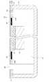
最初に、図1〜図3を参照しながら本発明の実施例1を説明する。本発明は、例えば、携帯電話やスマートフォン,あるいは、カーナビゲーション装置やゲーム機など、表示装置とそれに付随するタッチパネル機能を備えた電子機器に対し、入力を触覚で感知せしめるハプティック機能を実装する技術に関するものであるが、本実施例では、前記電子機器としてスマートフォンを例示して説明する。図1は、本実施例のスマートフォンを示す図であり、(A)は全体の外観斜視図,(B)はパネル表示部の分解斜視図である。図2は、前記図1(A)を#A−#A線に沿って切断し矢印方向に見た圧電振動素子の実装部分の断面図であり、図3は、前記図1(B)を#B−#B線に沿って切断し矢印方向に見た圧電振動素子の断面図である。 First, Embodiment 1 of the present invention will be described with reference to FIGS. The present invention relates to a technique for mounting a haptic function that senses an input with a tactile sensation for an electronic device having a display device and a touch panel function associated therewith, such as a mobile phone, a smartphone, a car navigation device, or a game machine. However, in the present embodiment, a smartphone will be exemplified and described as the electronic device. 1A and 1B are diagrams showing a smartphone according to the present embodiment, in which FIG. 1A is an overall perspective view of the appearance, and FIG. 1B is an exploded perspective view of a panel display unit. 2 is a cross-sectional view of the mounting portion of the piezoelectric vibration element when FIG. 1A is cut along the line # A- # A and viewed in the direction of the arrow, and FIG. 3 is a cross-sectional view of FIG. It is sectional drawing of the piezoelectric vibration element cut | disconnected along the # B- # B line | wire and seeing in the arrow direction.
図1及び図2に示すように、本実施例のスマートフォン10は、筐体12の収納部14内に、表示装置18及びタッチパネル20が配置されており、表面のほぼ全面が透明な保護パネル22(保護基板)で覆われた構成となっており、該保護パネル22は、筐体12の縁部16に支持されている。なお、透明とは、保護基板を通して、該保護基板の背面に設けられた表示部で表示された内容が視覚的に判別できることをいう。前記保護パネル22には、受話用の放音孔24や操作用スイッチ26のための開口部28が設けられている。なお、画像等が実際に表示される表示領域46は、前記保護パネル22の中央部の制限された範囲となっている。前記保護パネル22は、表面側の第1のガラス基板22Aと、前記タッチパネル20側の第2のガラス基板22Bを接合した接合基板となっており、前記第1のガラス基板22A及び第2のガラス基板22Bとしては、化学的に強化された強化ガラス等が用いられる。なお、本発明では、タッチパネル装置を視覚的に見る方向を、表面側(上側ないし上)と定義し、反対方向を、背面側(下側ないし下)と定義する。 As shown in FIGS. 1 and 2, in the
前記保護パネル22の下(ないし背面側)には、前記タッチパネル20が設けられる。該タッチパネル20としては、静電容量式のほか、抵抗膜方式などの公知の既存の方式を用いることができる。更に、タッチパネル20の下には前記表示装置18が配置されているが、該表示装置18(表示部)についても、液晶表示装置のほか、有機ELを用いた表示装置等が利用可能である。前記保護パネル22とタッチパネル20の間、該タッチパネル20と表示装置18の間は、それぞれ図示しない光学的に透明な接着剤や粘着テープなどによって固定されている。前記接着剤としては、エポキシをはじめとする一般的な材料が用いられ、また、粘着剤としては、アクリル系粘着剤をはじめとする一般的な材料が用いられる。 The
また、前記保護パネル22には、圧電振動素子40が実装されている。本実施例では、下側のガラス基板22Bに、2ヶ所の段差部30A,30B(本実施例では、凹部30A,30Bとも表記する)を設け、その部分に圧電振動素子40を実装する。段差部30A,30B(本実施例では、凹部30A,30B)の段差は、前記圧電振動素子40の厚みよりも深くしている。前記圧電振動素子40の厚みとは、該圧電振動素子40が振動するときの変位量を考慮し、圧電振動素子40が振動しないときの厚みと、変位量とを少なくとも合わせたものである。該圧電振動素子40は、上面が上側のガラス基板22Aに対して接着剤や粘着剤,あるいは、両面テープなどを用いて接合され、底面側が前記凹部30A,30Bの底面により支持されている。本実施例では、圧電振動素子40の平面形状が長方形であるが、その両端部を強固に固定し、中央部は柔らかく固定することにより、発生した振動を効率よくガラス基板22に伝達させることができる。そのために、例えば、周辺(ないし両端部)の接合部にはエポキシなどの接着剤や、基材がPETなどの両面テープを用いることが望ましく、中央部の接合にはウレタンやシリコンなどの柔らかい接着剤や、基材がゴムやエラストマーでできた柔らかい両面テープを用いることが望ましい。前記凹部30A,30Bの寸法は、圧電振動素子40の寸法に応じて決定される。 A
前記保護パネル22の厚みは、実装する装置等の構成によっても異なるが、ガラス基板22A及び22Bを貼り合わせた状態で1mm以下となることが一般的であり、本実施例では、下側のガラス基板22Bよりも、上側のガラス基板22Aの厚さを薄くすることで、より少ない力での振動伝達を可能としている。また、前記圧電振動素子40の実装位置は、図2に示すように前記タッチパネル20の配置されている範囲外であるため、圧電振動素子40の振動がタッチパネル20によって妨げられることがない。 Although the thickness of the
次に、前記圧電振動素子40について説明する。圧電振動素子40は、図3に示すように、複数の圧電体層42と電極層44を交互に積層した構造となっており、本実施例では、厚み方向中心の上側40Aと下側40Bで、電界に対する分極方向が逆になるように分極したバイモルフ構造のものを利用した。該圧電振動素子40は、実装する電子機器の構造にもよるが、全く積層していない単板構造としてもよいし、積層する場合でも、電界に対して全ての圧電体層が同じ方向に分極されているユニモルフ構造を採用することも可能であるが、入力電圧を低く抑えるという観点からは積層構造とする方が望ましく、また、発生変位や発生力を大きくするという観点からはバイモルフ構造とすることが望ましい。前記圧電体層42の材料としては、例えば、チタン酸ジルコン酸鉛に添加物を加えた圧電材料が用いられるが、一般的に知られている圧電セラミックスであれば、他の材料を用いてもよい。電極層44の材料としては、例えば、銀や白金など、公知の各種の電極材料が利用可能である。 Next, the
前記圧電振動素子40は、保護パネル22のガラス基板22Bに埋め込むように実装することから、発生変位・発生力や保護パネル22として必要な厚みを確保することを合わせて考えると、厚みは0.4〜0.6mmとすることが望ましい。また、圧電振動素子40の長さと幅は、実装する電子機器の構成によるが、本実施例で例示しているスマートフォン10では、例えば、長さを60mm以下、幅を5mm以下とすることが望ましく、更に、十分に振動をガラス面に伝達するためには、幅は2mm以上とすることが好ましい。本実施例では、上記寸法範囲を考慮し、圧電振動素子40の厚さを0.5mm,長さを50mm,幅を3mmとした。また、圧電体層42は、一層あたりの厚みを18μmとし、26層積層することとした。 Since the
前記圧電振動素子40の表面に形成された電極層44には、図示しない駆動回路が接続されるが、接続用の電路は、ガラス基板22A,22Bの表面に印刷やスパッタリングなどの方法で設けるようにしてもよいし、極細の金属線で形成してもよい。以上のような圧電振動素子40を実装した保護パネル22と、タッチパネル20,表示装置18を貼り合わせることにより、本発明に係るハプティック機能を有するタッチパネル装置(ないしパネル表示部)が形成される。 A drive circuit (not shown) is connected to the
次に、本実施例の作用を説明する。前記表示領域46に表示された表示内容に応じた位置の保護パネル22が押されると、前記タッチパネル20が押下されることを検出し、それに合わせて前記圧電振動素子40に信号を入力して振動させる。ガラス基板22Bの凹部30A,30B内で圧電振動素子40が振動するとき、該圧電振動素子40の周囲(側面部側)のガラスの厚みは、上方のガラスの厚み(ガラス基板22Aの厚み)と比べて厚く剛性が高いため、振動は表面弾性波となり、保護パネル22を押した指やスタイラスペンのペン先に振動が伝達される。このため、ガラス基板(保護パネル22)を厚み方向全体で振動する場合に比較して、少ないパワーでも、触覚的にスイッチ押下を感知させることが可能となる。 Next, the operation of this embodiment will be described. When the
このとき入力される信号としては、単純な正弦波信号や矩形波信号,あるいは、それらの組み合わせでもよいし、上述した背景技術の特許文献5に示されるようなスイッチ押下を錯覚させるような信号であってもよい。本実施例では、2つの圧電振動素子40を用いているため、各々に入力される信号の振幅や位相を制御することにより、保護パネル22の面内の特定の場所に強い振幅を誘起することができ、指などが触れている部分を選択的に振動させることが可能となる。 The signal input at this time may be a simple sine wave signal, a rectangular wave signal, or a combination thereof, or a signal that causes the illusion of switch pressing as shown in Patent Document 5 of the background art described above. There may be. In the present embodiment, since two
このような構造のタッチパネル装置(パネル表示部)を用い、入力信号として、人間の指先の感度が最も高いとされる200Hzの正弦波信号を用いて、保護パネル22の変位量を測定した。また、同じタッチパネル装置を用いて100Hzの正弦波信号を入力し、保護パネル22の表面から10cmの位置においたマイクによって発生する音を測定した。その結果、変位量に関しては、入力電圧8Vrmsで4μmの変位量が得られた。また、音圧は90dBと高かった。比較例として、圧電振動素子40を表示装置18の下側に配置した構造のタッチパネル装置を作製し、同様の方法で変位量と音圧を測定した。その結果、同じ入力電圧8Vrmsで変位は0.3μm,音圧は70dBであり、実施例に比べて変位量及び音圧とも大幅に低下することが確認された。 Using the touch panel device (panel display unit) having such a structure, a displacement amount of the
このように、実施例1によれば、次のような効果がある。
(1)表示装置18やタッチパネル20を保護する透明な保護パネル22を、2枚のガラス基板22A,22Bの接合により構成し、タッチパネル20側のガラス基板22Bの接合面側に圧電振動素子40の厚みよりも深い凹部30A,30Bを設けて、該凹部30A,30B内に圧電振動素子40を配置して表面側のガラス基板22Aに接合することとした。そのため、圧電振動素子40の振動は、表面弾性波として保護パネル22の表面に伝わり、わずかな力や変位であっても、保護パネル22の表面に十分な振動をさせ、指先などに確実に振動を伝達する。また、タッチパネル装置の薄型化を図りながら、ハプティック機能の実装が可能となる。Thus, according to the first embodiment, there are the following effects.
(1) A transparent
(2)ガラス基板22Bに設けた凹部30A,30Bの底面によって圧電振動素子40の底面側を支持するため、タッチパネル20と重なっていない部分に圧電振動素子40を設けることができるため、タッチパネル20による振動の妨げを防止することができる。
(3)表面側のガラス基板22Aを、タッチパネル側のガラス基板22Bよりも薄くしたので、より小さい力でも振動の伝達が可能となる。
(4)圧電振動素子40を2ヶ所に設けたので、各々に入力される信号の振幅や位相を制御することにより、保護パネル22の面内の特定の場所に強い振幅を誘起することができ、指などが触れている部分を選択的に振動させることが可能となる。(2) Since the bottom surface side of the
(3) Since the
(4) Since the piezoelectric vibrating
(5)圧電振動素子40の平面形状を長方形とし、その両端部を強固に固定し、中央部は柔らかく固定することとしたので、発生した振動を効率よく保護パネル22に伝達させることができる。
(6)圧電振動素子40が、圧電体層42と電極層44を複数交互に積層した積層構造であるため、入力電圧を低く抑えることができる。
(7)圧電振動素子40をバイモルフ構造としたので、発生変位や発生力を大きくすることができる。(5) Since the planar shape of the
(6) Since the
(7) Since the
なお、本発明は、上述した実施例に限定されるものではなく、本発明の要旨を逸脱しない範囲内において種々変更を加え得ることができる。例えば、以下のものも含まれる。
(1)前記実施例で示した形状,寸法などは一例であり、必要に応じて適宜変更してよい。例えば、前記実施例では、圧電振動素子40の形状を長方形とし、その寸法の具体例を示したが、これも一例であり、圧電振動素子40の長さ,幅,厚みは、同様の効果を奏する範囲内で適宜増減してよい。形状についても同様に、円形にするなど、適宜変更可能である。
(2)前記実施例で示した圧電振動素子40ではバイモルフ構造としたが、これも一例でありユニモルフ構造としてもよい。
(3)前記実施例では圧電振動素子40を積層構造としたが、これも一例であり、単板構造としてもよいし、積層構造とする場合も必要に応じて適宜積層数を増減してよい。In addition, this invention is not limited to the Example mentioned above, A various change can be added in the range which does not deviate from the summary of this invention. For example, the following are also included.
(1) The shapes, dimensions, etc. shown in the above embodiments are merely examples, and may be changed as appropriate. For example, in the above-described embodiment, the shape of the
(2) Although the piezoelectric vibrating
(3) In the above-described embodiment, the
(4)前記圧電振動素子40を形成する材料についても公知の各種の材料が利用可能である。
(5)圧電振動素子40の実装数も一例であり、前記実施例では2つ実装することとしたが、タッチパネル装置やそれを設ける電子機器(スマートフォン10など)の構成次第では、圧電振動素子40の実装数は1つとしてもよいし、3つ以上であってもよい。
(6)前記実施例では、凹部30A,30Bをタッチパネル20側のガラス基板22Bに設けることとしたが、表面側のガラス基板22Aに凹部を設けてその内側に圧電振動素子40を配置してもよい。(4) Various known materials can be used as the material for forming the
(5) The number of
(6) In the above-described embodiment, the
(7)前記実施例では、圧電振動素子40を凹部30A,30Bの底面で支持する構成としたが、これも一例であり、図4(A)に示す例のように、凹部の代わりに貫通孔50をガラス基板22Bに設け、その内側に配置した圧電振動素子40の底面とタッチパネル20の間に、柔らかい緩衝材52を設けることで、間接的にタッチパネル20で支持するようにしてもよい。前記緩衝材52を設けることにより、圧電振動素子40から保護パネル22への振動の伝達がタッチパネル20によって妨げられるのを防止することができる。前記緩衝材52の弾性率は、10〜100MPaが好ましい。 (7) In the above-described embodiment, the
(8)前記実施例で示した凹部30A,30Bの形状も一例であり、必要に応じて適宜変更してよい。例えば、図4(B)に示す例のように、ガラス基板22Bに、上方へ向かって広がる20°程度の傾きのテーパ面62を有する凹部(ないし段差部)60を形成し、その内側に圧電振動素子40を配置してもよい。前記テーパ面62を上に向けて広げることにより、振動の妨げが低減し、振動伝達の効率が向上する。
(9)前記実施例では、本発明のタッチパネル装置をスマートフォン10に適用することとしたが、これは一例であり、本発明は、携帯電話,カーナビゲーション装置,ゲーム機など、表示装置とそれに付随するタッチパネル機能を備えた電子機器全般に適用可能である。(8) The shape of the
(9) In the above embodiment, the touch panel device of the present invention is applied to the
本発明によれば、表示部やタッチパネルを保護する透明な保護基板を、第1及び第2のガラス基板の接合により構成し、該第1又は第2のガラス基板のいずれか一方のガラス基板の前記接合する面側に厚み方向に圧電振動素子の厚みより厚い段差部を有し、前記段差部に圧電振動素子を配置して第1のガラス基板に接合することで、わずかな力や変位であっても、保護基板表面への十分な振動の伝達が可能となるため、タッチパネル装置やそれを利用した電子機器の用途に適用できる。特に、薄型化が要望される機器等へのハプティック機能の実装に好適である。 According to the present invention, the transparent protective substrate that protects the display unit and the touch panel is configured by joining the first and second glass substrates, and either one of the first or second glass substrate is used. By having a step portion thicker than the thickness of the piezoelectric vibration element in the thickness direction on the surface to be joined, and disposing the piezoelectric vibration element in the step portion and joining to the first glass substrate, a slight force or displacement can be achieved. Even if it exists, since transmission of sufficient vibration to the surface of a protective substrate is attained, it can apply to the use of a touchscreen device or an electronic device using the same. In particular, it is suitable for mounting a haptic function to a device or the like that is required to be thin.
10:スマートフォン
12:筐体
14:収納部
16:縁部
18:表示装置
20:タッチパネル
22:保護パネル(保護基板)
22A,22B:ガラス基板
24:放音孔
26:操作用スイッチ
28:開口部
30A,30B:凹部(段差部)
40:圧電振動素子
40A:上側
40B:下側
42:圧電体層
44:電極層
46:表示領域
50:貫通孔
52:緩衝材
60:凹部(段差部)
62:テーパ面10: Smartphone 12: Housing 14: Storage unit 16: Edge 18: Display device 20: Touch panel 22: Protective panel (protective substrate)
22A, 22B: Glass substrate 24: Sound emission hole 26: Operation switch 28:
40:
62: Tapered surface
Claims (10)
Translated fromJapanese前記保護基板を、表面側の第1のガラス基板と前記タッチパネル側の第2のガラス基板の接合により構成するとともに、
前記第1又は第2のガラス基板のいずれか一方のガラス基板の前記接合される面側に厚み方向に前記圧電振動素子の厚みより厚い段差部を有し、前記段差部に前記圧電振動素子を配置し、該圧電振動素子を第1のガラス基板に接合したことを特徴とするタッチパネル装置。A touch panel device having a touch panel, a display unit provided on the back side of the touch panel, a transparent protective substrate formed on the surface side of the touch panel, and a piezoelectric vibration element,
The protective substrate is configured by bonding the first glass substrate on the front surface side and the second glass substrate on the touch panel side,
There is a step portion thicker than the thickness of the piezoelectric vibration element in the thickness direction on the side of the surface to be joined of one of the first or second glass substrates, and the piezoelectric vibration element is disposed on the step portion. A touch panel device, wherein the piezoelectric vibration element is disposed and bonded to a first glass substrate.
Priority Applications (2)
| Application Number | Priority Date | Filing Date | Title |
|---|---|---|---|
| JP2011071250AJP5597583B2 (en) | 2011-03-28 | 2011-03-28 | Touch panel device and electronic device |
| US13/431,619US8884897B2 (en) | 2011-03-28 | 2012-03-27 | Touch panel device and electronic device with improved haptic feedback |
Applications Claiming Priority (1)
| Application Number | Priority Date | Filing Date | Title |
|---|---|---|---|
| JP2011071250AJP5597583B2 (en) | 2011-03-28 | 2011-03-28 | Touch panel device and electronic device |
Publications (2)
| Publication Number | Publication Date |
|---|---|
| JP2012203895A JP2012203895A (en) | 2012-10-22 |
| JP5597583B2true JP5597583B2 (en) | 2014-10-01 |
Family
ID=46926541
Family Applications (1)
| Application Number | Title | Priority Date | Filing Date |
|---|---|---|---|
| JP2011071250AActiveJP5597583B2 (en) | 2011-03-28 | 2011-03-28 | Touch panel device and electronic device |
Country Status (2)
| Country | Link |
|---|---|
| US (1) | US8884897B2 (en) |
| JP (1) | JP5597583B2 (en) |
Cited By (1)
| Publication number | Priority date | Publication date | Assignee | Title |
|---|---|---|---|---|
| US11978276B2 (en) | 2020-05-13 | 2024-05-07 | Samsung Electronics Co., Ltd. | Electronic device comprising optical sensor module |
Families Citing this family (52)
| Publication number | Priority date | Publication date | Assignee | Title |
|---|---|---|---|---|
| US8405618B2 (en)* | 2006-03-24 | 2013-03-26 | Northwestern University | Haptic device with indirect haptic feedback |
| JP5597583B2 (en)* | 2011-03-28 | 2014-10-01 | 太陽誘電株式会社 | Touch panel device and electronic device |
| JP5926950B2 (en)* | 2011-12-22 | 2016-05-25 | 京セラ株式会社 | Electronics |
| US20150062458A1 (en)* | 2012-03-29 | 2015-03-05 | Kyocera Corporation | Input device, display device, and electronic device |
| US9684382B2 (en) | 2012-06-13 | 2017-06-20 | Microsoft Technology Licensing, Llc | Input device configuration having capacitive and pressure sensors |
| US9459160B2 (en) | 2012-06-13 | 2016-10-04 | Microsoft Technology Licensing, Llc | Input device sensor configuration |
| JP5909682B2 (en)* | 2012-10-09 | 2016-04-27 | パナソニックIpマネジメント株式会社 | Electronics |
| JP5960587B2 (en)* | 2012-12-19 | 2016-08-02 | 京セラ株式会社 | Input device, display device, and electronic device |
| JP2014126949A (en) | 2012-12-25 | 2014-07-07 | Kyocera Corp | Portable terminal equipment, screen control method and program |
| JP6063734B2 (en) | 2012-12-25 | 2017-01-18 | 京セラ株式会社 | Mobile terminal device, unlocking method and program |
| WO2014104040A1 (en) | 2012-12-25 | 2014-07-03 | 京セラ株式会社 | Mobile terminal device |
| CN104903825B (en)* | 2013-01-18 | 2017-08-15 | 株式会社村田制作所 | Displacement detecting sensor and operation input unit |
| US10578499B2 (en)* | 2013-02-17 | 2020-03-03 | Microsoft Technology Licensing, Llc | Piezo-actuated virtual buttons for touch surfaces |
| US20140232679A1 (en)* | 2013-02-17 | 2014-08-21 | Microsoft Corporation | Systems and methods to protect against inadvertant actuation of virtual buttons on touch surfaces |
| JP6133619B2 (en)* | 2013-02-22 | 2017-05-24 | 京セラ株式会社 | Vibration device, electronic device, and portable terminal |
| JP6001482B2 (en)* | 2013-03-25 | 2016-10-05 | 京セラ株式会社 | Input device and electronic device |
| SG11201510027RA (en) | 2013-06-07 | 2016-01-28 | 3M Innovative Properties Co | Method of forming a recess in a substrate, abrasive wheel, and cover |
| JP2015005426A (en)* | 2013-06-21 | 2015-01-08 | 株式会社東芝 | Non-aqueous electrolyte battery |
| WO2014208691A1 (en) | 2013-06-26 | 2014-12-31 | 京セラ株式会社 | Portable device and method for controlling portable device |
| JP5820846B2 (en)* | 2013-07-11 | 2015-11-24 | 太陽誘電株式会社 | Vibrating device and electronic device using the same |
| JP5914426B2 (en)* | 2013-07-18 | 2016-05-11 | 京セラ株式会社 | Electronics |
| JP5815612B2 (en)* | 2013-07-29 | 2015-11-17 | 京セラ株式会社 | Electronics |
| CN105378614B (en)* | 2013-08-06 | 2019-05-21 | 株式会社村田制作所 | Pressing detection sensors |
| EP3072169B1 (en) | 2013-11-21 | 2020-01-01 | 3M Innovative Properties Company | Multi-layer piezoelectric polymer film device |
| WO2015098090A1 (en)* | 2013-12-26 | 2015-07-02 | 京セラ株式会社 | Electronic instrument |
| JP6272022B2 (en)* | 2013-12-26 | 2018-01-31 | 京セラ株式会社 | Electronics |
| US9448631B2 (en) | 2013-12-31 | 2016-09-20 | Microsoft Technology Licensing, Llc | Input device haptics and pressure sensing |
| DE102014000829B4 (en)* | 2014-01-21 | 2019-02-28 | Harald Kobolla | Portable computer with a haptic output device |
| JP6046064B2 (en) | 2014-01-29 | 2016-12-14 | 京セラ株式会社 | Mobile device, touch position correction method and program |
| JP2015153406A (en)* | 2014-02-19 | 2015-08-24 | Fdk株式会社 | Tactile transmission device |
| JP6360367B2 (en) | 2014-06-26 | 2018-07-18 | 京セラ株式会社 | Portable electronic device, control method and program for portable electronic device |
| JP2016080465A (en)* | 2014-10-15 | 2016-05-16 | 日本写真印刷株式会社 | Pressure detector |
| KR101655923B1 (en)* | 2014-12-09 | 2016-09-08 | 엘지전자 주식회사 | Sensor-actuator for touch input device and terminal using the same |
| US10416799B2 (en) | 2015-06-03 | 2019-09-17 | Microsoft Technology Licensing, Llc | Force sensing and inadvertent input control of an input device |
| US10222889B2 (en) | 2015-06-03 | 2019-03-05 | Microsoft Technology Licensing, Llc | Force inputs and cursor control |
| JP6062519B1 (en) | 2015-09-28 | 2017-01-18 | 京セラ株式会社 | Electronic device and method of operating electronic device |
| DE102015226321A1 (en) | 2015-12-21 | 2017-06-22 | Zf Friedrichshafen Ag | Gear selector switch for a motor vehicle and method for detecting actuation of a gear selector switch for a motor vehicle |
| JP6143838B2 (en)* | 2015-12-24 | 2017-06-07 | 京セラ株式会社 | Electronics |
| US10061385B2 (en) | 2016-01-22 | 2018-08-28 | Microsoft Technology Licensing, Llc | Haptic feedback for a touch input device |
| US10206044B2 (en)* | 2016-09-08 | 2019-02-12 | Microsoft Technology Licensing, Llc | Display structure having a visual display and an audio output |
| FR3061568B1 (en)* | 2017-01-04 | 2021-09-10 | Hap2U | VIBRATING TOUCH SLAB |
| JP6732688B2 (en)* | 2017-03-30 | 2020-07-29 | 京セラ株式会社 | Display device |
| DE102017212011B3 (en)* | 2017-07-13 | 2018-11-22 | Bayerische Motoren Werke Aktiengesellschaft | Display device and motor vehicle with display device |
| KR102420554B1 (en) | 2017-08-10 | 2022-07-14 | 삼성디스플레이 주식회사 | Display panel, bracket and display device comprising the same |
| CN107506092B (en)* | 2017-09-30 | 2021-02-19 | 联想(北京)有限公司 | Input control method and terminal |
| JP6609649B2 (en)* | 2018-01-22 | 2019-11-20 | 株式会社丸和製作所 | Tactile sense imparting device and program |
| JP6604391B2 (en)* | 2018-01-22 | 2019-11-13 | 株式会社丸和製作所 | Actuator |
| JP7243517B2 (en)* | 2019-08-09 | 2023-03-22 | Tdk株式会社 | vibration unit |
| JP7429506B2 (en) | 2019-08-29 | 2024-02-08 | 太陽誘電株式会社 | Vibration panels and electronic equipment |
| JP7360281B2 (en)* | 2019-09-10 | 2023-10-12 | 株式会社東海理化電機製作所 | Control device, control method, and program |
| CN111124127B (en)* | 2019-12-25 | 2021-08-20 | 吉林大学 | Method and device for tactile rendering of digital keys based on vibration and lamination effect |
| CN115867877A (en)* | 2020-08-31 | 2023-03-28 | 阿尔卑斯阿尔派株式会社 | Input device |
Family Cites Families (48)
| Publication number | Priority date | Publication date | Assignee | Title |
|---|---|---|---|---|
| US6087198A (en)* | 1998-02-12 | 2000-07-11 | Texas Instruments Incorporated | Low cost packaging for thin-film resonators and thin-film resonator-based filters |
| JP3992840B2 (en)* | 1998-06-22 | 2007-10-17 | 北陸電気工業株式会社 | Piezoelectric sounder and manufacturing method thereof |
| JP2001218001A (en)* | 2000-02-04 | 2001-08-10 | Ricoh Co Ltd | Document reading device |
| KR100522528B1 (en)* | 2000-10-13 | 2005-10-19 | 가부시키가이샤 덴소 | Touch panel and display device |
| JP4527315B2 (en)* | 2001-05-14 | 2010-08-18 | セイコーインスツル株式会社 | Display device |
| JP3834494B2 (en)* | 2001-09-19 | 2006-10-18 | 株式会社ケンウッド | Piezoelectric speaker device |
| JP2004129223A (en)* | 2002-07-31 | 2004-04-22 | Murata Mfg Co Ltd | Piezoelectric component and manufacturing method thereof |
| JP2004125571A (en)* | 2002-10-01 | 2004-04-22 | National Institute Of Advanced Industrial & Technology | Transparent piezoelectric sensor and input device having the same |
| JP2004127073A (en)* | 2002-10-04 | 2004-04-22 | Smk Corp | Instruction input device |
| JP2004163262A (en)* | 2002-11-13 | 2004-06-10 | Touch Panel Systems Kk | Acoustic wave contact detector |
| JP4177142B2 (en)* | 2003-03-10 | 2008-11-05 | 富士通コンポーネント株式会社 | Coordinate input device and drive device |
| DE602004013534D1 (en)* | 2004-03-09 | 2008-06-19 | Infineon Technologies Ag | Acoustic volume wave filter and method for avoiding unwanted side passages |
| US20060097996A1 (en)* | 2004-11-10 | 2006-05-11 | Alps Electric Co., Ltd. | Input device |
| JP2006146611A (en) | 2004-11-19 | 2006-06-08 | Fujitsu Component Ltd | Haptic panel device |
| JP2007065800A (en)* | 2005-08-29 | 2007-03-15 | Seiko Epson Corp | Touch panel device |
| JP2007086990A (en)* | 2005-09-21 | 2007-04-05 | Smk Corp | Touch panel |
| DE102005051289B3 (en)* | 2005-10-26 | 2007-05-16 | Siemens Ag | Piezoelectric actuator and method for producing the same |
| US8780053B2 (en)* | 2007-03-21 | 2014-07-15 | Northwestern University | Vibrating substrate for haptic interface |
| US20100141580A1 (en)* | 2007-08-22 | 2010-06-10 | Oh Eui Jin | Piezo-electric sensing unit and data input device using piezo-electric sensing |
| US8457325B2 (en)* | 2007-11-06 | 2013-06-04 | Magna International, Inc. | Acoustical window assembly for vehicle |
| CN102265246B (en)* | 2008-12-22 | 2015-05-27 | 京瓷株式会社 | input device |
| EP2202619A1 (en) | 2008-12-23 | 2010-06-30 | Research In Motion Limited | Portable electronic device including tactile touch-sensitive input device and method of controlling same |
| JP2010157037A (en) | 2008-12-26 | 2010-07-15 | Nissha Printing Co Ltd | Panel member having oscillating element |
| US8760413B2 (en)* | 2009-01-08 | 2014-06-24 | Synaptics Incorporated | Tactile surface |
| CN102333737A (en)* | 2009-02-25 | 2012-01-25 | 精工电子有限公司 | Glass substrate polishing method, package manufacturing method, piezoelectric oscillator, oscillator, electronic device, and radio-controlled watch |
| US9696803B2 (en)* | 2009-03-12 | 2017-07-04 | Immersion Corporation | Systems and methods for friction displays and additional haptic effects |
| JP5343871B2 (en)* | 2009-03-12 | 2013-11-13 | 株式会社リコー | Touch panel device, display device with touch panel including the same, and control method for touch panel device |
| EP3410262A1 (en)* | 2009-03-12 | 2018-12-05 | Immersion Corporation | System and method for providing features in a friction display |
| DE102009015991A1 (en)* | 2009-04-02 | 2010-10-07 | Pi Ceramic Gmbh Keramische Technologien Und Bauelemente | Device for generating a haptic feedback of a keyless input unit |
| CN102439549A (en)* | 2009-04-06 | 2012-05-02 | 3M创新有限公司 | Touch sensor with modular sensing components |
| US8493364B2 (en)* | 2009-04-30 | 2013-07-23 | Motorola Mobility Llc | Dual sided transparent display module and portable electronic device incorporating the same |
| CN101893977B (en)* | 2009-05-19 | 2012-07-25 | 北京京东方光电科技有限公司 | Touch screen, color film base plate and manufacture method thereof |
| US10401961B2 (en) | 2009-06-09 | 2019-09-03 | Immersion Corporation | Method and apparatus for generating haptic effects using actuators |
| JP2011002926A (en) | 2009-06-17 | 2011-01-06 | Hitachi Ltd | Display device with tactile exhibition function |
| KR101667801B1 (en)* | 2009-06-19 | 2016-10-20 | 삼성전자주식회사 | Touch panel and electronic device including the touch panel |
| KR20110024531A (en)* | 2009-09-02 | 2011-03-09 | 삼성모바일디스플레이주식회사 | Organic light emitting display device |
| EP2325733B1 (en)* | 2009-11-02 | 2013-06-12 | SMK Corporation | Holding structure for a touch panel |
| JP4811965B2 (en)* | 2009-11-02 | 2011-11-09 | Smk株式会社 | Touch panel holding structure |
| EP2325731B1 (en)* | 2009-11-02 | 2013-11-13 | SMK Corporation | Holding structure for a touch panel |
| KR20110111031A (en)* | 2010-04-02 | 2011-10-10 | 삼성전자주식회사 | Composite touch screen panel device |
| JP2011242386A (en)* | 2010-04-23 | 2011-12-01 | Immersion Corp | Transparent compound piezoelectric material aggregate of contact sensor and tactile sense actuator |
| JP5026574B2 (en)* | 2010-04-27 | 2012-09-12 | 日本電波工業株式会社 | Piezoelectric device |
| JP5580155B2 (en)* | 2010-09-27 | 2014-08-27 | スタンレー電気株式会社 | Method for manufacturing touch panel input device |
| US9143668B2 (en)* | 2010-10-29 | 2015-09-22 | Apple Inc. | Camera lens structures and display structures for electronic devices |
| US8467177B2 (en)* | 2010-10-29 | 2013-06-18 | Apple Inc. | Displays with polarizer windows and opaque masking layers for electronic devices |
| US8780060B2 (en)* | 2010-11-02 | 2014-07-15 | Apple Inc. | Methods and systems for providing haptic control |
| KR101289648B1 (en)* | 2010-11-10 | 2013-07-30 | 엘지디스플레이 주식회사 | Electrophoresis display device having a touch screen and method for driving the touch screen |
| JP5597583B2 (en)* | 2011-03-28 | 2014-10-01 | 太陽誘電株式会社 | Touch panel device and electronic device |
- 2011
- 2011-03-28JPJP2011071250Apatent/JP5597583B2/enactiveActive
- 2012
- 2012-03-27USUS13/431,619patent/US8884897B2/enactiveActive
Cited By (1)
| Publication number | Priority date | Publication date | Assignee | Title |
|---|---|---|---|---|
| US11978276B2 (en) | 2020-05-13 | 2024-05-07 | Samsung Electronics Co., Ltd. | Electronic device comprising optical sensor module |
Also Published As
| Publication number | Publication date |
|---|---|
| US8884897B2 (en) | 2014-11-11 |
| US20120249459A1 (en) | 2012-10-04 |
| JP2012203895A (en) | 2012-10-22 |
Similar Documents
| Publication | Publication Date | Title |
|---|---|---|
| JP5597583B2 (en) | Touch panel device and electronic device | |
| JP5820846B2 (en) | Vibrating device and electronic device using the same | |
| JP4697095B2 (en) | Touch panel display device, electronic device and game device | |
| CN103282868B (en) | Electronic equipment | |
| KR101187980B1 (en) | Haptic feedback device and electronic device including the same | |
| JP5833028B2 (en) | System and method for haptic feedback using laterally driven piezoelectric actuators | |
| JP2022106937A (en) | Flexible vibration module and display device including the same | |
| US9740288B2 (en) | Electronic device | |
| JP4229098B2 (en) | Touch panel display device, electronic device including touch panel display device, and camera including touch panel display device | |
| JP6055612B2 (en) | Electronics | |
| WO2010150563A1 (en) | Electronic device | |
| JP6073071B2 (en) | Electronics | |
| CN102917299A (en) | Screen sounder | |
| JP2008186188A (en) | Touch panel display device, production method therefor and electronic device | |
| WO2012114763A1 (en) | Electronic device | |
| JPWO2016035628A1 (en) | Vibration device | |
| JP5738105B2 (en) | Touch panel device and electronic device | |
| JP6133619B2 (en) | Vibration device, electronic device, and portable terminal | |
| KR20210018703A (en) | Display device | |
| JP4604902B2 (en) | INPUT / OUTPUT DEVICE AND ELECTRONIC DEVICE HAVING INPUT / OUTPUT DEVICE | |
| WO2012137443A1 (en) | Electronic apparatus | |
| JP5894850B2 (en) | Panel device | |
| JP5816130B2 (en) | Panel device | |
| JP2013008151A (en) | Electronic apparatus and portable terminal with the same | |
| JP2010245842A (en) | Bending vibration actuator |
Legal Events
| Date | Code | Title | Description |
|---|---|---|---|
| A621 | Written request for application examination | Free format text:JAPANESE INTERMEDIATE CODE: A621 Effective date:20131122 | |
| A977 | Report on retrieval | Free format text:JAPANESE INTERMEDIATE CODE: A971007 Effective date:20140618 | |
| TRDD | Decision of grant or rejection written | ||
| A01 | Written decision to grant a patent or to grant a registration (utility model) | Free format text:JAPANESE INTERMEDIATE CODE: A01 Effective date:20140805 | |
| A61 | First payment of annual fees (during grant procedure) | Free format text:JAPANESE INTERMEDIATE CODE: A61 Effective date:20140811 | |
| R150 | Certificate of patent or registration of utility model | Ref document number:5597583 Country of ref document:JP Free format text:JAPANESE INTERMEDIATE CODE: R150 | |
| R250 | Receipt of annual fees | Free format text:JAPANESE INTERMEDIATE CODE: R250 | |
| R250 | Receipt of annual fees | Free format text:JAPANESE INTERMEDIATE CODE: R250 | |
| R250 | Receipt of annual fees | Free format text:JAPANESE INTERMEDIATE CODE: R250 | |
| R250 | Receipt of annual fees | Free format text:JAPANESE INTERMEDIATE CODE: R250 | |
| R250 | Receipt of annual fees | Free format text:JAPANESE INTERMEDIATE CODE: R250 | |
| R250 | Receipt of annual fees | Free format text:JAPANESE INTERMEDIATE CODE: R250 | |
| R250 | Receipt of annual fees | Free format text:JAPANESE INTERMEDIATE CODE: R250 | |
| R250 | Receipt of annual fees | Free format text:JAPANESE INTERMEDIATE CODE: R250 | |
| R250 | Receipt of annual fees | Free format text:JAPANESE INTERMEDIATE CODE: R250 |