JP5590874B2 - Nitride semiconductor device - Google Patents
Nitride semiconductor deviceDownload PDFInfo
- Publication number
- JP5590874B2 JP5590874B2JP2009287938AJP2009287938AJP5590874B2JP 5590874 B2JP5590874 B2JP 5590874B2JP 2009287938 AJP2009287938 AJP 2009287938AJP 2009287938 AJP2009287938 AJP 2009287938AJP 5590874 B2JP5590874 B2JP 5590874B2
- Authority
- JP
- Japan
- Prior art keywords
- nitride semiconductor
- ohmic
- recess portion
- semiconductor layer
- ohmic recess
- Prior art date
- Legal status (The legal status is an assumption and is not a legal conclusion. Google has not performed a legal analysis and makes no representation as to the accuracy of the status listed.)
- Expired - Fee Related
Links
Images


Classifications
- H—ELECTRICITY
- H10—SEMICONDUCTOR DEVICES; ELECTRIC SOLID-STATE DEVICES NOT OTHERWISE PROVIDED FOR
- H10D—INORGANIC ELECTRIC SEMICONDUCTOR DEVICES
- H10D30/00—Field-effect transistors [FET]
- H10D30/40—FETs having zero-dimensional [0D], one-dimensional [1D] or two-dimensional [2D] charge carrier gas channels
- H10D30/47—FETs having zero-dimensional [0D], one-dimensional [1D] or two-dimensional [2D] charge carrier gas channels having 2D charge carrier gas channels, e.g. nanoribbon FETs or high electron mobility transistors [HEMT]
- H10D30/471—High electron mobility transistors [HEMT] or high hole mobility transistors [HHMT]
- H10D30/475—High electron mobility transistors [HEMT] or high hole mobility transistors [HHMT] having wider bandgap layer formed on top of lower bandgap active layer, e.g. undoped barrier HEMTs such as i-AlGaN/GaN HEMTs
- H—ELECTRICITY
- H10—SEMICONDUCTOR DEVICES; ELECTRIC SOLID-STATE DEVICES NOT OTHERWISE PROVIDED FOR
- H10D—INORGANIC ELECTRIC SEMICONDUCTOR DEVICES
- H10D62/00—Semiconductor bodies, or regions thereof, of devices having potential barriers
- H10D62/40—Crystalline structures
- H10D62/405—Orientations of crystalline planes
- H—ELECTRICITY
- H10—SEMICONDUCTOR DEVICES; ELECTRIC SOLID-STATE DEVICES NOT OTHERWISE PROVIDED FOR
- H10D—INORGANIC ELECTRIC SEMICONDUCTOR DEVICES
- H10D64/00—Electrodes of devices having potential barriers
- H10D64/20—Electrodes characterised by their shapes, relative sizes or dispositions
- H10D64/23—Electrodes carrying the current to be rectified, amplified, oscillated or switched, e.g. sources, drains, anodes or cathodes
- H10D64/251—Source or drain electrodes for field-effect devices
- H10D64/256—Source or drain electrodes for field-effect devices for lateral devices wherein the source or drain electrodes are recessed in semiconductor bodies
- H—ELECTRICITY
- H10—SEMICONDUCTOR DEVICES; ELECTRIC SOLID-STATE DEVICES NOT OTHERWISE PROVIDED FOR
- H10D—INORGANIC ELECTRIC SEMICONDUCTOR DEVICES
- H10D62/00—Semiconductor bodies, or regions thereof, of devices having potential barriers
- H10D62/80—Semiconductor bodies, or regions thereof, of devices having potential barriers characterised by the materials
- H10D62/85—Semiconductor bodies, or regions thereof, of devices having potential barriers characterised by the materials being Group III-V materials, e.g. GaAs
- H10D62/8503—Nitride Group III-V materials, e.g. AlN or GaN
Landscapes
- Junction Field-Effect Transistors (AREA)
- Electrodes Of Semiconductors (AREA)
Description
Translated fromJapanese本発明は、窒化物半導体素子およびその製造方法に関する。 The present invention relates to a nitride semiconductor device and a method for manufacturing the same.
窒化ガリウム(GaN)をはじめとするIII族窒化物半導体は、シリコン(Si)や砒化ガリウム(GaAs)よりも禁制帯幅や電子の飽和速度が大きく絶縁破壊電界が高い。このため、III族窒化物半導体を材料として用いた高周波大電力の電界効果トランジスタ(Field Effect Transistor:FET)などの開発が活発に行われている。 Group III nitride semiconductors such as gallium nitride (GaN) have a larger forbidden band width and higher electron saturation rate than silicon (Si) and gallium arsenide (GaAs) and a higher dielectric breakdown electric field. For this reason, development of a high-frequency, high-power field effect transistor (FET) using a group III nitride semiconductor as a material has been actively conducted.
III族窒化物半導体FETには結晶成長の容易さからウルツ鉱構造の結晶を用いるが、このときAlGaNとGaNとでヘテロ接合界面を作製すると、圧電分極と自発分極によって界面に電荷が形成される。これにより、不純物をドーピングしなくともヘテロ接合界面近傍に2次元電子ガスが形成される。III族窒化物半導体FETにおいてはこれを電子の通り道であるチャネルとして利用する。 A group III nitride semiconductor FET uses a wurtzite structure crystal for ease of crystal growth. At this time, if a heterojunction interface is made of AlGaN and GaN, a charge is formed at the interface due to piezoelectric polarization and spontaneous polarization. . As a result, a two-dimensional electron gas is formed in the vicinity of the heterojunction interface without doping impurities. In the group III nitride semiconductor FET, this is used as a channel which is a path for electrons.
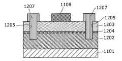
次に、図10を用いて一般的な窒化物半導体FETの構造について説明する。まず、有機金属化学気相成長法(MOCVD法)によって、基板1101上にGaNチャネル層1102、AlGaNバリア層1103を順次成長する。このとき、前述のようにGaNチャネル層1102のAlGaNバリア層1103とのヘテロ界面近傍に、図10の点線部のように、2次元電子ガスによるチャネル1104が形成されている。 Next, the structure of a general nitride semiconductor FET will be described with reference to FIG. First, a GaN
次に、AlGaNバリア層1103上にゲート電極1108と、ソース、ドレインとして用いるオーミック電極1107を作製する。このとき、AlGaNバリア層1103が電子に対する大きなポテンシャル障壁として働くため、オーミック電極1107からチャネル1104への電子の流入を妨げる。このためにオーミック電極1107におけるコンタクト抵抗が増大する。 Next, a
そこで、図11のように、AlGaNバリア層1203をGaNチャネル層1202に到達するまでドライエッチングし、オーミックリセス部1205を形成することでチャネル1204を露出させ、チャネル1204に直接オーミック電極1207を接触させることがコンタクト抵抗の低減に効果的であることについて開示されている(たとえば、特許文献1参照)。 Therefore, as shown in FIG. 11, the AlGaN
また、ドライエッチングにより、AlGaNバリア層1203を貫いて、AlGaNバリア層1203の表面からチャネル1204より深い位置のGaNチャネル層1202までオーミックリセス部1205を形成し、オーミックリセス部1205の側面の面積を増大させることが、コンタクト抵抗の低減に有効であることについて開示されている(たとえば、特許文献2参照)。 Further, by dry etching, an
しかしながら、ドライエッチングによりオーミックリセス部の形成を行った場合、オーミックリセス部側面の面積は増大するが、ドライエッチングによってオーミックリセス部の側面に結晶欠陥が形成されて高抵抗層となることがある。この高抵抗層により、コンタクト抵抗が増大する。 However, when the ohmic recess portion is formed by dry etching, the area of the side surface of the ohmic recess portion is increased, but crystal defects may be formed on the side surface of the ohmic recess portion by dry etching to form a high resistance layer. This high resistance layer increases the contact resistance.
本発明は、かかる課題を解決し、オーミック電極とオーミックリセス部とのコンタクト抵抗を低減した窒化物半導体素子および窒化物半導体素子の製造方法を提供することを目的とする。 An object of the present invention is to solve such problems and to provide a nitride semiconductor device and a method for manufacturing the nitride semiconductor device in which the contact resistance between the ohmic electrode and the ohmic recess portion is reduced.
上記の目的を達成するため、本発明の一形態における窒化物半導体素子は、基板上に形成された第1の窒化物半導体層と、前記第1の窒化物半導体層上に形成され、前記第1の窒化物半導体層と比べてバンドギャップが大きい第2の窒化物半導体層と、少なくとも前記第2の窒化物半導体層に形成されたオーミックリセス部と、前記オーミックリセス部に接触して設けられたオーミック電極とを備え、前記オーミックリセス部は、前記オーミック電極と接触する面の少なくとも一部に凹凸構造を有する。 In order to achieve the above object, a nitride semiconductor device according to an aspect of the present invention is formed on a first nitride semiconductor layer formed on a substrate, the first nitride semiconductor layer, and the first nitride semiconductor layer. A second nitride semiconductor layer having a band gap larger than that of the first nitride semiconductor layer, at least an ohmic recess formed in the second nitride semiconductor layer, and in contact with the ohmic recess The ohmic recess portion has a concavo-convex structure on at least a part of a surface in contact with the ohmic electrode.
この構成によれば、オーミックリセス部の端面(壁面、底面)の少なくとも一部に凹凸構造を有するので、オーミックリセス部の表面積が大きくなる。したがって、オーミック電極とオーミックリセス部との接触面積を増大して、オーミック電極とオーミックリセス部とのコンタクト抵抗を低減することができる。 According to this configuration, since the concavo-convex structure is provided on at least a part of the end surface (wall surface, bottom surface) of the ohmic recess portion, the surface area of the ohmic recess portion is increased. Therefore, the contact area between the ohmic electrode and the ohmic recess portion can be increased, and the contact resistance between the ohmic electrode and the ohmic recess portion can be reduced.
ここで、前記凹凸構造は、ウェットエッチングにより形成されているようにしてもよい。 Here, the uneven structure may be formed by wet etching.
この構成によれば、ウェットエッチングにより、結晶欠陥による高抵抗層を除去するとともに、オーミックリセス部の端面(壁面、底面)の少なくとも一部に凹凸構造を形成することができる。したがって、オーミック電極とオーミックリセス部との接触面積を増大してコンタクト抵抗を低減することができる。 According to this configuration, the high resistance layer due to crystal defects can be removed by wet etching, and a concavo-convex structure can be formed on at least a part of the end face (wall surface, bottom face) of the ohmic recess portion. Therefore, the contact area between the ohmic electrode and the ohmic recess portion can be increased to reduce the contact resistance.
ここで、前記凹凸構造は、主に(−1100)面と(01−10)面とからなる三角形状により構成されているようにしてもよい。 Here, the concavo-convex structure may be configured by a triangular shape mainly including a (−1100) plane and a (01-10) plane.
また、前記第1の窒化物半導体層および前記第2の窒化物半導体層は、<0001>方向に積層され、前記凹凸構造は、前記オーミックリセス部において<11−20>方向と垂直な面に形成されているようにしてもよい。 The first nitride semiconductor layer and the second nitride semiconductor layer are stacked in a <0001> direction, and the concavo-convex structure is on a plane perpendicular to the <11-20> direction in the ohmic recess portion. It may be formed.
また、前記第1の窒化物半導体層および前記第2の窒化物半導体層は、<1−100>方向に積層され、前記凹凸構造は、前記オーミックリセス部において<11−20>方向と垂直な面に形成されているようにしてもよい。 The first nitride semiconductor layer and the second nitride semiconductor layer are stacked in a <1-100> direction, and the concavo-convex structure is perpendicular to the <11-20> direction in the ohmic recess portion. It may be formed on the surface.
また、前記第1の窒化物半導体層および前記第2の窒化物半導体層は、<11−20>方向に積層され、前記凹凸構造は、前記オーミックリセス部において<11−20>方向と垂直な面に形成されているようにしてもよい。 The first nitride semiconductor layer and the second nitride semiconductor layer are stacked in a <11-20> direction, and the uneven structure is perpendicular to the <11-20> direction in the ohmic recess portion. It may be formed on the surface.
この構成によれば、結晶格子の(−1100)面と(01−10)面とを利用して、(−1100)面と(01−10)面とからなる三角形状の微小な凹凸構造を形成することができる。 According to this configuration, by using the (−1100) plane and the (01-10) plane of the crystal lattice, a triangular fine concavo-convex structure composed of the (−1100) plane and the (01-10) plane is formed. Can be formed.
また、前記凹凸構造は、前記オーミックリセス部において<1−100>方向と垂直な面に、<11−20>方向と平行に形成された(10−10)面を含む溝形状により構成されているようにしてもよい。 The concavo-convex structure is configured by a groove shape including a (10-10) plane formed in parallel to the <11-20> direction on a plane perpendicular to the <1-100> direction in the ohmic recess portion. You may make it.
この構成によれば、結晶格子の(10−10)面を利用して、<11−20>方向と平行に溝形状の微小な凹凸構造を形成することができる。 According to this configuration, it is possible to form a groove-shaped minute concavo-convex structure in parallel with the <11-20> direction by using the (10-10) plane of the crystal lattice.
また、上記課題を解決するために本発明の一形態における窒化物半導体素子の製造方法は、オーミック電極を有する窒化物半導体素子の製造方法であって、基板上に第1の窒化物半導体層を形成する工程と、前記第1の窒化物半導体層上に、前記第1の窒化物半導体層と比べてバンドギャップが大きい第2の窒化物半導体層を形成する工程と、少なくとも前記第2の窒化物半導体層にオーミックリセス部を形成する工程と、前記オーミックリセス部において前記オーミック電極と接触される面の少なくとも一部に、凹凸構造を形成する工程とを含む。 In order to solve the above problems, a method for manufacturing a nitride semiconductor device according to an embodiment of the present invention is a method for manufacturing a nitride semiconductor device having an ohmic electrode, wherein the first nitride semiconductor layer is provided on a substrate. Forming a second nitride semiconductor layer having a band gap larger than that of the first nitride semiconductor layer on the first nitride semiconductor layer, and at least the second nitride semiconductor layer. A step of forming an ohmic recess in the physical semiconductor layer, and a step of forming a concavo-convex structure on at least a part of the surface in contact with the ohmic electrode in the ohmic recess.
この構成によれば、オーミックリセス部の端面(壁面、底面)の少なくとも一部に凹凸構造が形成されるので、オーミックリセス部の表面積が大きくなる。したがって、オーミック電極とオーミックリセス部との接触面積を増大して、オーミック電極とオーミックリセス部とのコンタクト抵抗を低減することができる。 According to this configuration, since the concavo-convex structure is formed on at least a part of the end surface (wall surface, bottom surface) of the ohmic recess portion, the surface area of the ohmic recess portion is increased. Therefore, the contact area between the ohmic electrode and the ohmic recess portion can be increased, and the contact resistance between the ohmic electrode and the ohmic recess portion can be reduced.
ここで、前記凹凸構造を形成する工程において、前記凹凸構造はウェットエッチングにより形成されるようにしてもよい。 Here, in the step of forming the concavo-convex structure, the concavo-convex structure may be formed by wet etching.
この構成によれば、ウェットエッチングにより、結晶欠陥による高抵抗層を除去するとともに、オーミックリセス部の端面(壁面、底面)の少なくとも一部に凹凸構造を形成することができる。したがって、オーミック電極とオーミックリセス部との接触面積を増大してコンタクト抵抗を低減することができる。 According to this configuration, the high resistance layer due to crystal defects can be removed by wet etching, and a concavo-convex structure can be formed on at least a part of the end face (wall surface, bottom face) of the ohmic recess portion. Therefore, the contact area between the ohmic electrode and the ohmic recess portion can be increased to reduce the contact resistance.
ここで、前記オーミックリセス部に、前記オーミック電極を接触して形成する工程をさらに含むようにしてもよい。 Here, a step of forming the ohmic electrode in contact with the ohmic recess may be further included.
この構成によれば、微小な凹凸構造を有するオーミックリセス部の端面(壁面、底面)にオーミック電極が接触して形成されるので、オーミック電極とオーミックリセス部との接触面積を増大してコンタクト抵抗を低減することができる。 According to this configuration, since the ohmic electrode is formed in contact with the end face (wall surface, bottom surface) of the ohmic recess portion having a minute concavo-convex structure, the contact resistance between the ohmic electrode and the ohmic recess portion is increased and contact resistance is increased. Can be reduced.
本発明にかかる窒化物半導体素子によれば、オーミック電極とオーミックリセス部とのコンタクト抵抗を低減することができる。 According to the nitride semiconductor device of the present invention, the contact resistance between the ohmic electrode and the ohmic recess portion can be reduced.
以下、本発明にかかる窒化物半導体素子の実施の形態について、図面を参照しながら説明する。なお、本発明について、以下の実施の形態および添付の図面を用いて説明を行うが、これは例示を目的としており、本発明がこれらに限定されることを意図しない。 Embodiments of a nitride semiconductor device according to the present invention will be described below with reference to the drawings. In addition, although this invention is demonstrated using the following embodiment and attached drawing, this is for the purpose of illustration and this invention is not intended to be limited to these.
(実施の形態1)
本発明の実施の形態1にかかる窒化物半導体素子の構成について説明する。本実施の形態では、基板上に形成された第1の窒化物半導体層と、第1の窒化物半導体層上に形成され、第1の窒化物半導体層と比べてバンドギャップが大きい第2の窒化物半導体層と、少なくとも第2の窒化物半導体層に形成されたオーミックリセス部と、オーミックリセス部に接触して設けられたオーミック電極とを備え、オーミックリセス部は、オーミック電極と接触する面の少なくとも一部に凹凸構造を有する窒化物半導体素子について説明する。これにより、オーミック電極とオーミックリセス部とのコンタクト抵抗を低減することができる。(Embodiment 1)
The configuration of the nitride semiconductor device according to the first embodiment of the present invention will be described. In the present embodiment, the first nitride semiconductor layer formed on the substrate and the second nitride semiconductor layer formed on the first nitride semiconductor layer and having a larger band gap than the first nitride semiconductor layer. A nitride semiconductor layer, an ohmic recess formed in at least the second nitride semiconductor layer, and an ohmic electrode provided in contact with the ohmic recess, wherein the ohmic recess is in contact with the ohmic electrode A nitride semiconductor device having a concavo-convex structure at least in part will be described. Thereby, the contact resistance between the ohmic electrode and the ohmic recess portion can be reduced.
まず、本願発明者が見出した、従来よりもコンタクト抵抗を低減する方法について示す。 First, a method for reducing contact resistance as compared with the prior art discovered by the present inventors will be described.
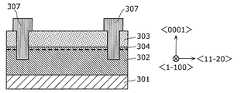
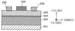
図1Aに示すように、有機金属化学気相成長(MOCVD)法により、シリコン(Si)もしくは窒化ガリウム(GaN)、サファイア、もしくはシリコンカーバイド(SiC)からなる基板301の主面上に、膜厚が2μmのGaNチャネル層302、膜厚が25nm(10〜500nm)のたとえばAl0.30Ga0.70NからなるAlGaNバリア層303を順次成長する。AlGaNバリア層303のバンドギャップは、GaNチャネル層302のバンドギャップよりも大きい。これにより、GaNチャネル層302とAlGaNバリア層303とのヘテロ接合界面には、2次元電子ガスによるチャネル304が形成される。GaNチャネル層302は、窒化物半導体AlxInyGa1-x-yN(0≦x≦1、0≦y≦1、0≦x+y≦1)において、x=0、y=0とした窒化物半導体からなるチャネル層、Al0.30Ga0.70Nは、x=0.30、y=0とした窒化物半導体からなるバリア層である。As shown in FIG. 1A, a film thickness is formed on the main surface of a
次に、所定のパターンを有するマスクをAlGaNバリア層303の上面に配置して、AlGaNバリア層303をドライエッチングすることにより、図1Bに示すように、凹状のオーミックリセス部305が形成される。オーミックリセス部305は、図1Cに示すように、FETのソース電極、ドレイン電極であるオーミック電極307をGaNチャネル層302、AlGaNバリア層303に接触して設けるための、コンタクト部分である。オーミックリセス部305は、AlGaNバリア層303の上面からAlGaNバリア層303を貫通してGaNチャネル層302に凹状に形成され、図1Bに示すように、壁面305aと底面305bを有する。以上により、窒化物半導体素子を構成する積層構造体306が形成される。 Next, a mask having a predetermined pattern is disposed on the upper surface of the
この際、前記オーミックリセス部305の壁面305aには、ドライエッチングにより高抵抗層が形成される。つまり、オーミックリセス部305はドライエッチングにより形成されたため、オーミックリセス部305の壁面はエッチングにより結晶欠陥が発生することがある。この結晶欠陥により、オーミックリセス部305の壁面は高抵抗化し、この高抵抗化された高抵抗層によりコンタクト抵抗が上昇する。そこで、コンタクト抵抗の低減のため、ウェットエッチングなどにより高抵抗層を除去する必要がある。 At this time, a high resistance layer is formed on the
高抵抗層の除去は、積層構造体306を、25℃、濃度0.1mol/lの水酸化カリウム(KOH)溶液に40分間浸しウェットエッチングを行う。これにより、前記オーミックリセス部305は、横方向、つまり、壁面305aと垂直な方向にエッチングされ、高抵抗層が除去される。 The high resistance layer is removed by dipping the
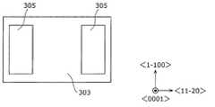
図2Aおよび図2Bは、それぞれウェットエッチング前後の積層構造体306の上面図である。 2A and 2B are top views of the
図2Aに示した窒化物半導体素子の上面図のように、オーミックリセス部305の長手方向の端面を<1−100>方向に実質的に平行に形成すると、KOH溶液でウェットエッチング処理することで、図2Bのような凹凸構造が形成される。具体的には、<11−20>方向に垂直な面と<1−100>方向に垂直な面では、面方位が異なるため、エッチングにより形成される凹凸構造が異なる。 As shown in the top view of the nitride semiconductor device shown in FIG. 2A, when the end face in the longitudinal direction of the
図3は、図2Bに示した窒化物半導体素子の上面図の詳細な説明のための図である。
ここで、図3(a)は、窒化物半導体AlxInyGa1-x-yN(0≦x≦1、0≦y≦1、0≦x+y≦1)の面方位を示している。AlxInyGa1-x-yNは、ウルツ鉱構造の結晶であり、図3(a)に示すように、サファイアやSiC等と同様の六方晶系結晶構造の結晶面の表記により面方位が定められる。また、図3(b)に示すように、オーミックリセス部305は、AlGaNバリア層303の上面から見て、<1−100>方向に長手方向を有する長方形状に、2箇所に形成される。FIG. 3 is a diagram for explaining in detail the top view of the nitride semiconductor device shown in FIG. 2B.
Here, FIG. 3A shows the plane orientation of the nitride semiconductor Alx Iny Ga1-xy N (0 ≦ x ≦ 1, 0 ≦ y ≦ 1, 0 ≦ x + y ≦ 1). Alx Iny Ga1-xy N is a wurtzite crystal, and as shown in FIG. 3 (a), the crystal orientation of the crystal plane of the hexagonal crystal structure is similar to that of sapphire or SiC. Determined. Further, as shown in FIG. 3B, the
上記したように、オーミックリセス部305の壁面305aをKOH溶液によりウェットエッチング処理する場合、オーミックリセス部305の壁面305aには、微小な凹凸構造が形成される。これは、ウェットエッチングにより、オーミックリセス部305の壁面305aにおいて、AlxInyGa1-x-yNが結晶格子単位でエッチングされ、図3(b)に示すように、<11−20>方向と垂直なオーミックリセス部305の壁面305aでは(−1100)面および(01−10)面からなるファセットが、<1−100>方向と垂直なオーミックリセス部305の壁面305aでは(10−10)面を含むファセットが露出するためである。As described above, when the
これにより、オーミックリセス部305において<11−20>方向と垂直なオーミックリセス部305の壁面305aには、図3(b)に示すように、上面から見て主に(−1100)面と(01−10)面とからなる、一辺が30nm或いは約10nm〜500nmほどの微小な三角形状の凹凸構造が形成される。このとき、オーミックリセス部305の長手方向が完全に<1−100>方向と平行でない場合であっても、AlxInyGa1-x-yNは結晶格子単位でエッチングされるので、KOH溶液によるウェットエッチング処理により(−1100)面と(01−10)面とからなる三角形状の凹凸構造が形成される。(−1100)面と(01−10)面とからなる三角形状の一辺は、KOH溶液のモル濃度が高いほど長くなり、たとえば、KOH溶液のモル濃度が3mol/lのとき三角形状の一辺は100nmほど、0.1mol/lのときには30nmほどとなる。Thus, in the
また、オーミックリセス部305において<1−100>方向と垂直なオーミックリセス部305の壁面305aには、(10−10)面を含む溝形状が<11−20>方向と平行に多数形成される。このため、<1−100>方向と垂直なオーミックリセス部305の壁面305aは、図3(b)に示すように、上面から見てほぼ直線状((10−10)面と実質的に平行)となる。なお、ウェットエッチングに用いる溶液はKOHに限らず、NaOHなどその他のアルカリ系溶液を用いてもよい。 Further, in the
オーミック電極307とオーミックリセス部305とのコンタクト抵抗を低減するには、オーミック電極307とオーミックリセス部305との接触面積が大きいほうがよく、オーミックリセス部305の壁面305aに凹凸構造を設けることは、接触面積を増大するのに効果的である。一方、凹凸構造が大きいと、電界が凹凸構造に集中してデバイスが破壊されることがある。したがって、電界集中を防止するためには凹凸構造は微小なほうがよく、三角形状の一辺は可能な限り小さいほうがよい。微小な凹凸構造をするために、たとえば、電子線(Electron Beam:EB)露光により数nmオーダーの微細な形状をレジストにパターニングし、その後レジストマスクによりドライエッチングを行う方法も挙げられる。しかし、この場合、ドライエッチングやレジストの剥離等により、形成されたパターンの壁面には多量の結晶欠陥が形成されてしまう。この欠陥により、コンタクト抵抗は高くなる。また、パターンの壁面の結晶欠陥を除去しようとして本手法以外のウェットエッチングにより欠陥除去を行うと、形成された微細なパターンがエッチングにより消失してしまう。しかし、発明者らは、本手法により一辺が数十nmから数百nmほどの三角形状からなる微細な形状を自己形成させることができることを見出した。 In order to reduce the contact resistance between the
なお、ドライエッチングにより形成されたオーミックリセス部305の長手方向の壁面305aは、上記した実施の形態に示したように<1−100>方向と平行でなくてもよい。<1−100>方向に対して、−45°〜45°程度傾いていても、オーミックリセス部305の壁面305aおよび底面305bは、ウェットエッチングにより結晶格子単位でエッチングされるため、オーミックリセス部305の壁面305aおよび底面305bには、微小な凹凸構造を形成することができるため、本発明の効果を奏する。 Note that the
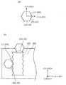
ここで、KOH溶液エッチングによるコンタクト抵抗低減の効果を調べるため、オーミックリセス部305を<11−20>方向と<1−100>方向に矩形に形成し、KOH溶液で40分間処理し、<1−100>方向、<11−20>方向に通電した場合のTLM(Transfer Lign Method:TLM)によるコンタクト抵抗の評価を実施した。 Here, in order to examine the effect of contact resistance reduction by KOH solution etching,
図4は、矩形のオーミックリセス部305を0.1mol/lの濃度で25℃のKOH溶液にて40分間ウェットエッチングし、オーミックリセス部305に、たとえば、図1Cに示すように、Ti/Alからなるオーミック電極307を形成し、オーミック電極307の通電端面をそれぞれ<1−100>方向、<11−20>方向として通電を行った場合のコンタクト抵抗値を示す。 FIG. 4 shows that a rectangular
図4より、KOH溶液によるウェットエッチング処理を行った場合は、<11−20>方向に通電を行った場合のコンタクト抵抗値(0.9Ω・mm程度)のほうが、<1−100>方向に通電を行った場合のコンタクト抵抗値(1.1Ω・mm程度)よりも明瞭に低かった。これは、<11−20>方向では、上記したように(−1100)面と(01−10)面とからなる三角形状の凹凸構造が形成され、<1−100>方向よりも表面積が増大しているので、コンタクト抵抗が下がったことによる。また、KOH溶液処理を行わなかった場合、オーミックリセス部305の壁面305aにドライエッチングに伴う結晶欠陥が発生し、これにより高抵抗化したためコンタクトがとれなかった。 As shown in FIG. 4, when the wet etching process using the KOH solution is performed, the contact resistance value (about 0.9 Ω · mm) in the <11-20> direction is more in the <1-100> direction. It was clearly lower than the contact resistance value (about 1.1 Ω · mm) when energized. This is because, in the <11-20> direction, a triangular concavo-convex structure composed of the (−1100) plane and the (01-10) plane is formed as described above, and the surface area is larger than in the <1-100> direction. This is because the contact resistance has decreased. In addition, when the KOH solution treatment was not performed, crystal defects associated with dry etching occurred on the
次に、本願発明者が見出したコンタクト抵抗を低減する条件を適用した窒化物半導体素子について以下に説明する。 Next, a nitride semiconductor device to which the condition for reducing the contact resistance found by the present inventor is applied will be described below.
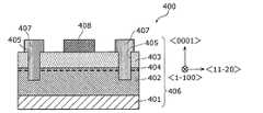
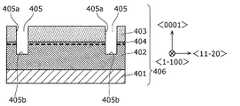
図5は、本実施の形態にかかる窒化物半導体素子400の構成を示す断面図である。
図5に示すように、本実施の形態にかかる窒化物半導体素子400は、基板401と、第1の窒化物半導体層であるGaNチャネル層402と、第2の窒化物半導体層であるAlGaNバリア層403と、オーミックリセス部405とにより構成される積層構造体406と、オーミック電極407と、ゲート電極408とを備えている。AlGaNバリア層403のバンドギャップは、GaNチャネル層402のバンドギャップよりも大きく、GaNチャネル層402とAlGaNバリア層403とのヘテロ界面近傍には、2次元電子ガスによるチャネル404が形成されている。FIG. 5 is a cross-sectional view showing the configuration of the
As shown in FIG. 5, the
図6A〜図6Dは、本実施の形態にかかる窒化物半導体素子400の製造工程を示す断面図である。 6A to 6D are cross-sectional views illustrating the manufacturing process of the
図6Aに示すように、MOCVD法により、Si、GaN、サファイア、SiCなどからなる基板401の主面上に、膜厚が2μmのGaNチャネル層402、膜厚が25nm(10〜500nm)のAl0.30Ga0.70NからなるAlGaNバリア層403を+c面方向(<0001>方向)に順次成長する。このとき、前記GaNチャネル層402の一部には、2次元電子ガスによるチャネル404が形成される。なお、基板401の主面は、GaNチャネル層402およびAlGaNバリア層403が+c面方向に成長する面となっている。また、基板401がGaNからなる場合は、基板401とGaNチャネル層402との間に、バッファ層が必要となる。バッファ層は、高抵抗なAlNが好ましいが、AlGaN、GaNでもよい。また、基板401がSi、サファイア、SiCからなる場合も、同様に、基板401とGaNチャネル層402との間に、GaN、AlGaN、AlN等からなるバッファ層を形成してもよい。As shown in FIG. 6A, a
次に、図6Bに示すように、所定のパターンを有するマスクを配置してAlGaNバリア層403をドライエッチングしてオーミックリセス部405を形成する。このとき、前記オーミックリセス部405は長手方向が<1−100>方向に実質的に平行となるように形成する。また、オーミックリセス部405は、AlGaNバリア層403を貫通し、GaNチャネル層402は貫通せず、2次元電子ガスによるチャネル404よりも下まで届くように形成する。 Next, as shown in FIG. 6B, a mask having a predetermined pattern is disposed, and the
以上により形成された積層構造体406を、25℃、0.1mol/lの濃度のKOH溶液に40分間浸し、ウェットエッチングを行う。これにより、ドライエッチングによる結晶欠陥により形成された高抵抗層が除去されると同時に、オーミックリセス部405の<11−20>方向と垂直な壁面405aには(−1100)面と(01−10)面とからなるファセットによる凹凸構造が形成される。 The
次に、図6Cに示すように、オーミックリセス部405を覆うように、たとえばTi/Alからなるオーミック電極407を形成する。オーミック電極407は、オーミックリセス部405の壁面405aにおいて、AlGaNバリア層403およびGaNチャネル層402に接し、オーミックリセス部405の底面405bにおいて、GaNチャネル層402に接する。 Next, as shown in FIG. 6C, an
次に、図6Dに示すように、たとえばNi/Auからなるゲート電極408を形成する。このとき、ゲート電極408は<1−100>方向、つまり、オーミックリセス部405に形成されたオーミック電極407の長手方向と平行な方向に長手方向を有する直方体状に形成する。オーミック電極407およびゲート電極408は、たとえば、スパッタリング法により形成される。 Next, as shown in FIG. 6D, a
以上により、オーミックリセス部405をKOH溶液にてウェットエッチングし、オーミックリセス部405の壁面405aに形成された高抵抗層を除去すると同時に、オーミックリセス部405の壁面405aに形成された微小な凹凸構造により、たとえば結晶欠陥部分に電界が集中するのを抑制しつつ、オーミックリセス部405の壁面405aとオーミック電極407との接触面積を増大して、コンタクト抵抗を従来のものよりも低減することができる。 As described above, the
なお、オーミックリセス部405はAlGaNバリア層403を貫通しなくても、AlGaNバリア層403のみに凹状に形成されてもよい。この場合であっても、オーミックリセス部405の壁面405aにおけるAlGaNバリア層403には微小な凹凸構造が形成されるため、本発明の効果を奏する。 The
また、凹凸構造は、オーミックリセス部405の壁面405aに限らず底面405bにも形成されてもよい。この場合、底面405bでもオーミックリセス部405とオーミック電極407との接触面積がより増大するため、コンタクト抵抗がさらに低減される。 The uneven structure may be formed not only on the
(実施の形態2)
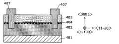
次に、本発明の実施の形態2について説明する。実施の形態2が実施の形態1と異なる点は、実施の形態1において結晶成長が+c面方向(<0001>方向)になされていたものが、実施の形態2においては結晶成長が+m面方向(<1−100>方向)になされている点である。実施の形態2においては、実施の形態1の場合と同様、オーミックリセス部の壁面の表面積を増大させることによってコンタクト抵抗低減が可能となる。(Embodiment 2)
Next, a second embodiment of the present invention will be described. The second embodiment is different from the first embodiment in that the crystal growth in the first embodiment is in the + c plane direction (<0001> direction), but the crystal growth in the second embodiment is in the + m plane direction. (<1-100> direction). In the second embodiment, as in the case of the first embodiment, the contact resistance can be reduced by increasing the surface area of the wall surface of the ohmic recess portion.
図7A〜図7Dは、本実施の形態にかかる窒化物半導体素子の製造工程を示す断面図である。 7A to 7D are cross-sectional views illustrating the manufacturing steps of the nitride semiconductor device according to the present embodiment.
図7Aに示すように、MOCVD法により、Si、GaN、サファイア、SiCなどからなる基板501の主面上に、膜厚が2μmのGaNチャネル層502、膜厚が25nm(10〜500nm)のSiドーピングを行った、n型Al0.30Ga0.70NからなるAlGaNバリア層503を、+m面方向(<1−100>方向)に順次成長する。このとき、SiドーピングによってAlGaNバリア層503とGaNチャネル層502とのヘテロ界面には電界が発生し、ヘテロ界面に電荷が引き寄せられる。これにより、GaNチャネル層502の一部には、2次元電子ガスによるチャネル504が形成される。As shown in FIG. 7A, a
なお、基板501の主面は、GaNチャネル層502およびAlGaNバリア層503が+m面方向に成長する面となっている。基板501がGaNからなる場合は、基板501とGaNチャネル層502との間に、バッファ層が必要となる。バッファ層は、高抵抗なAlNが好ましいが、AlGaN、GaNでもよい。また、基板501がSi、サファイア、SiCからなる場合も、同様に、基板501とGaNチャネル層502との間に、GaN、AlGaN、AlN等からなるバッファ層を形成してもよい。 The main surface of the
次に、図7Bに示すように、所定のパターンを有するマスクを配置してAlGaNバリア層503をドライエッチングしてオーミックリセス部505を形成する。このとき、前記オーミックリセス部505は長手方向が<0001>方向に実質的に平行となるように形成する。また、オーミックリセス部505は、AlGaNバリア層503を貫通し、GaNチャネル層502は貫通せず、2次元電子ガスによるチャネル504よりも下まで届くように形成する。 Next, as shown in FIG. 7B, a mask having a predetermined pattern is disposed, and the
以上により形成された積層構造体506を、25℃、0.1mol/lの濃度のKOH溶液に40分間浸し、ウェットエッチングを行う。これにより、ドライエッチングによる結晶欠陥により形成された高抵抗層が除去されると同時に、オーミックリセス部505の<11−20>方向と垂直な壁面505aには(−1100)面と(01−10)面とからなるファセットによる凹凸構造が形成される。 The
次に、図7Cに示すように、オーミックリセス部505を覆うように、たとえばTi/Alからなるオーミック電極507を形成する。オーミック電極507は、オーミックリセス部505の壁面505aにおいて、AlGaNバリア層503およびGaNチャネル層502に接し、オーミックリセス部505の底面505bにおいて、GaNチャネル層502に接する。 Next, as shown in FIG. 7C, an
次に、図7Dに示すように、たとえばNi/Auからなるゲート電極508を形成する。このとき、ゲート電極508は<0001>方向、つまり、オーミックリセス部505に形成されたオーミック電極507の長手方向と平行な方向に長手方向を有する直方体状に形成する。オーミック電極507およびゲート電極508は、たとえば、スパッタリング法により形成される。 Next, as shown in FIG. 7D, a
以上により、オーミックリセス部505をKOH溶液にてウェットエッチングし、オーミックリセス部505の壁面505aに形成された高抵抗層を除去すると同時に、オーミックリセス部505の壁面505aに形成された微小な凹凸構造により、たとえば結晶欠陥部分に電界が集中するのを抑制しつつ、オーミックリセス部505の壁面505aとオーミック電極507との接触面積を増大して、コンタクト抵抗を従来のものよりも低減することができる。 As described above, the
(実施の形態3)
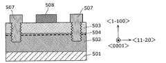
次に、本発明の実施の形態3について説明する。実施の形態3が実施の形態1と異なる点は、本実施の形態にかかる窒化物半導体素子において、オーミックリセス部が第2の窒化物半導体層であるAlGaNバリア層のみに形成される点である。実施の形態1においては、オーミックリセス部の壁面における表面積の増大を図ったが、オーミックリセス部の底面がAlGaN/GaN界面よりも表面側に位置する場合、オーミックリセス部の底面から電流が流れる。このため、オーミックリセス部の底面の表面積が増大することにより電流が流れやすくなるため、コンタクト抵抗低減が可能となる。(Embodiment 3)
Next, a third embodiment of the present invention will be described. The third embodiment is different from the first embodiment in that, in the nitride semiconductor device according to the present embodiment, the ohmic recess portion is formed only in the AlGaN barrier layer that is the second nitride semiconductor layer. . In the first embodiment, the surface area of the wall surface of the ohmic recess portion is increased. However, when the bottom surface of the ohmic recess portion is located on the surface side of the AlGaN / GaN interface, a current flows from the bottom surface of the ohmic recess portion. For this reason, since the current flows easily by increasing the surface area of the bottom surface of the ohmic recess portion, the contact resistance can be reduced.
以下、実施の形態3にかかる窒化物半導体素子600について、製造方法と共に説明する。 Hereinafter, the
図8は本実施の形態にかかる窒化物半導体素子600の構成を示す断面図である。
図8に示すように、本実施の形態にかかる窒化物半導体素子600は、基板601と、第1の窒化物半導体層であるGaNチャネル層602と、第2の窒化物半導体層であるAlGaNバリア層603と、オーミックリセス部607と、オーミック電極608と、ゲート電極609とを備えている。AlGaNバリア層603のバンドギャップは、GaNチャネル層602のバンドギャップよりも大きく、GaNチャネル層602とAlGaNバリア層603とのヘテロ界面近傍には、2次元電子ガスによるチャネル604が形成されている。FIG. 8 is a cross-sectional view showing the configuration of the
As shown in FIG. 8, a
図9A〜図9Dは、本実施の形態にかかる窒化物半導体素子600の製造工程を示す断面図である。 9A to 9D are cross-sectional views showing the manufacturing process of the
図9Aに示すように、MOCVD法により、Si、GaN、サファイア、SiCなどからなる基板601の主面上に、膜厚が2μmのGaNチャネル層602、膜厚が25nm(10〜500nm)のSiドーピングを行った、n型Al0.30Ga0.70NからなるAlGaNバリア層603を、+a面方向(<11−20>方向)に順次成長する。このとき、SiドーピングによってAlGaNバリア層603とGaNチャネル層602とのヘテロ界面には電界が発生し、ヘテロ界面に電荷が引き寄せられる。これにより、GaNチャネル層602の一部には、2次元電子ガスによるチャネル604が形成される。As shown in FIG. 9A, a
なお、基板601の主面は、GaNチャネル層602およびAlGaNバリア層603が+a面方向に成長する面となっている。また、基板601がGaNからなる場合は、基板601とGaNチャネル層602との間に、バッファ層が必要となる。バッファ層は、高抵抗なAlNが好ましいが、AlGaN、GaNでもよい。また、基板601がSi、サファイア、SiCからなる場合も、同様に、基板601とGaNチャネル層602との間に、GaN、AlGaN、AlN等からなるバッファ層を形成してもよい。 The main surface of the
次に、図9Bに示すように、AlGaNバリア層603上に、たとえばSiO2からなるマスク605を形成する。マスク605は、AlGaNバリア層603上にSiO2層を設けた後、SiO2層の上面にレジストを塗布してパターニングを行うことにより、所定位置に凹部を形成する。その後、フッ酸によりウェットエッチングを行い、レジスト除去を行うことで、オーミックリセス部607を形成するようにマスク605のパターニングを行っている。これにより、積層構造体606が形成される。なお、オーミックリセス部607は、壁面607aと底面607bを有し、壁面607aはマスク605を構成する材料であるSiO2、底面607bはAlGaNバリア層603からなる構成となる。Next, as shown in FIG. 9B, a
以上により形成された積層構造体606を、25℃、0.1mol/lの濃度のKOH溶液に120分間浸し、ウェットエッチングを行う。これにより、ドライエッチングによる結晶欠陥により形成された高抵抗層が除去されると同時に、AlGaNバリア層603の<11−20>方向と垂直な表面に形成されたオーミックリセス部607の底面607bには、(−1100)面と(01−10)面とからなるファセット(1辺が約10nm〜500nm)による凹凸構造が形成される。 The
次に、図9Cに示すように、マスク605をフッ酸により除去し、所定のパターンを有するマスクを配置して、上記したオーミックリセス部607の底面607bの位置に、たとえばTi/Alからなるオーミック電極608を形成する。次に、図9Dに示すように、たとえばNi/Auからなるゲート電極609を形成する。オーミック電極608およびゲート電極609は、たとえば、スパッタリング法により形成される。 Next, as shown in FIG. 9C, the
以上により、オーミックリセス部607をKOH溶液にてウェットエッチングし、オーミックリセス部607の底面607bに形成された高抵抗層を除去すると同時に、オーミックリセス部607の底面607bに形成された微小な凹凸構造により、たとえば結晶欠陥部分に電界が集中するのを抑制しつつ、オーミックリセス部607の底面607bとオーミック電極608の接触面積を増大することが可能である。これにより、コンタクト抵抗を従来のものよりも低減することができる。 As described above, the
なお、本発明は、上記した実施形態に限定されるものではなく、本発明の要旨を逸脱しない範囲内で種々の改良、変形を行ってもよい。 In addition, this invention is not limited to above-described embodiment, You may perform a various improvement and deformation | transformation within the range which does not deviate from the summary of this invention.
たとえば、基板、第1の窒化物半導体層、第2の窒化物半導体層、マスクの材料は、上記した実施の形態に示した例に限らず適宜変更してもよい。たとえば、GaNチャネル層、AlGaNバリア層は、窒化物半導体AlxInyGa1-x-yN(0≦x≦1、0≦y≦1、0≦x+y≦1)のx、yを変更して各原子の割合を変更してもよいし、これらの材料に限らず、その他の窒化物半導体材料であってもよい。For example, the materials of the substrate, the first nitride semiconductor layer, the second nitride semiconductor layer, and the mask are not limited to the examples shown in the above-described embodiments, and may be changed as appropriate. For example, the GaN channel layer and the AlGaN barrier layer are obtained by changing x and y of the nitride semiconductor Alx Iny Ga1-xy N (0 ≦ x ≦ 1, 0 ≦ y ≦ 1, 0 ≦ x + y ≦ 1). The ratio of each atom may be changed, and not only these materials but also other nitride semiconductor materials may be used.
また、基板の種類は上記した実施の形態に示した例に限らず適宜変更してもよい。また、基板の主面は+c面(<0001>方向)、+a面(<11−20>方向)、+m面(<1−100>方向)に限らず、オフ角を有する面、つまり、面方位がウエハ面からずれたものであってもよい。基板がSi、サファイア、SiCからなる場合は、基板とGaNチャネル層との間に、GaN、AlGaN、AlN等からなるバッファ層を形成してもよい。 Further, the type of the substrate is not limited to the example shown in the above embodiment, and may be changed as appropriate. The main surface of the substrate is not limited to the + c plane (<0001> direction), the + a plane (<11-20> direction), and the + m plane (<1-100> direction). The orientation may deviate from the wafer surface. When the substrate is made of Si, sapphire, or SiC, a buffer layer made of GaN, AlGaN, AlN, or the like may be formed between the substrate and the GaN channel layer.
また、窒化物半導体素子の形成方法やエッチング方法は、上記した方法に限定されず、これらの方法を組み合わせたり、その他の方法であってもよい。 Further, the method of forming the nitride semiconductor element and the etching method are not limited to the above-described methods, and these methods may be combined or other methods may be used.
また、オーミックリセス部の長手方向の壁面は、上記した実施の形態に示したように<1−100>方向や<0001>方向と平行でなくてもよい。<1−100>方向や<0001>方向に対して、−45°〜45°程度傾いていても、オーミックリセス部の壁面および底面は、ウェットエッチングにより結晶格子単位でエッチングされるため、オーミックリセス部の長手方向の壁面および底面には、微小な凹凸構造を形成することができるため、本発明の効果を奏する。 Further, the wall surface in the longitudinal direction of the ohmic recess portion may not be parallel to the <1-100> direction or the <0001> direction as shown in the above-described embodiment. Even if it is inclined by about −45 ° to 45 ° with respect to the <1-100> direction or the <0001> direction, the wall surface and the bottom surface of the ohmic recess portion are etched in units of crystal lattices by wet etching. Since the minute concavo-convex structure can be formed on the wall surface and the bottom surface in the longitudinal direction of the portion, the effect of the present invention is achieved.
また、本発明にかかる窒化物半導体には、上記実施の形態における任意の構成要素を組み合わせて実現される別の実施の形態や、実施の形態に対して本発明の主旨を逸脱しない範囲で当業者が思いつく各種変形を施して得られる変形例や、本発明にかかる窒化物半導体素子を備えた各種デバイスなども本発明に含まれる。たとえば、本発明にかかる窒化物半導体素子を備えた高周波用デバイスも本発明に含まれる。 In addition, the nitride semiconductor according to the present invention is applicable to other embodiments realized by combining arbitrary constituent elements in the above-described embodiments and to the embodiments without departing from the gist of the present invention. Modifications obtained by performing various modifications conceived by a contractor and various devices including the nitride semiconductor element according to the present invention are also included in the present invention. For example, a high-frequency device including the nitride semiconductor device according to the present invention is also included in the present invention.
本発明にかかる窒化物半導体素子は、特に、高周波用のトランジスタおよびその製造方法等として有用である。 The nitride semiconductor device according to the present invention is particularly useful as a high-frequency transistor and a manufacturing method thereof.
301、401、501、601、1101 基板
302、402、502、602、1102、1202 GaNチャネル層(第1の窒化物半導体層)
303、403、503、603、1103,1203 AlGaNバリア層(第2の窒化物半導体層)
304、404、504、604、1104、1204 チャネル
305、405、505、607、1205 オーミックリセス部
307、407、507、608、1107、1207 オーミック電極
400、600 窒化物半導体素子301, 401, 501, 601, 1101
303, 403, 503, 603, 1103, 1203 AlGaN barrier layer (second nitride semiconductor layer)
304, 404, 504, 604, 1104, 1204
Claims (4)
Translated fromJapanese前記第1の窒化物半導体層上に形成され、前記第1の窒化物半導体層と比べてバンドギャップが大きい第2の窒化物半導体層と、
前記第2の窒化物半導体層の上面から貫通し、前記第1の窒化物半導体層に凹状に形成されたオーミックリセス部と、
前記オーミックリセス部に接触して設けられたオーミック電極とを備え、
前記オーミックリセス部は、前記オーミック電極と接触する面の少なくとも一部に、主に(−1100)面と(01−10)面とからなる三角形状により構成される凹凸構造を有し、
前記第1の窒化物半導体層および前記第2の窒化物半導体層は、<0001>方向に積層され、
前記凹凸構造は、前記オーミックリセス部において<11−20>方向と垂直な面に形成されている
窒化物半導体素子。A first nitride semiconductor layer formed on the substrate;
A second nitride semiconductor layer formed on the first nitride semiconductor layer and having a larger band gap than the first nitride semiconductor layer;
An ohmic recess portion penetrating from the upper surface of the second nitride semiconductor layer and formed in a concave shape in the first nitride semiconductor layer;
An ohmic electrode provided in contact with the ohmic recess portion;
The ohmic recess portion has a concavo-convex structure mainly formed by a triangular shape including a (−1100) plane and a (01-10) plane on at least a part of a surface in contact with the ohmic electrode,
The first nitride semiconductor layer and the second nitride semiconductor layer are stacked in a <0001> direction,
The concavo-convex structure is a nitride semiconductor device formed in a plane perpendicular to the <11-20> direction in the ohmic recess.
前記第1の窒化物半導体層上に形成され、前記第1の窒化物半導体層と比べてバンドギャップが大きい第2の窒化物半導体層と、
前記第2の窒化物半導体層の上面から貫通し、前記第1の窒化物半導体層に凹状に形成されたオーミックリセス部と、
前記オーミックリセス部に接触して設けられたオーミック電極とを備え、
前記オーミックリセス部は、前記オーミック電極と接触する面の少なくとも一部に、主に(−1100)面と(01−10)面とからなる三角形状により構成される凹凸構造を有し、
前記第1の窒化物半導体層および前記第2の窒化物半導体層は、<1−100>方向に積層され、
前記凹凸構造は、前記オーミックリセス部において<11−20>方向と垂直な面に形成されている
窒化物半導体素子。A first nitride semiconductor layer formed on the substrate;
A second nitride semiconductor layer formed on the first nitride semiconductor layer and having a larger band gap than the first nitride semiconductor layer;
An ohmic recess portion penetrating from the upper surface of the second nitride semiconductor layer and formed in a concave shape in the first nitride semiconductor layer;
An ohmic electrode provided in contact with the ohmic recess portion;
The ohmic recess portion has a concavo-convex structure mainly formed by a triangular shape including a (−1100) plane and a (01-10) plane on at least a part of a surface in contact with the ohmic electrode,
The first nitride semiconductor layer and the second nitride semiconductor layer are stacked in a <1-100> direction,
The concavo-convex structure is a nitride semiconductor device formed in a plane perpendicular to the <11-20> direction in the ohmic recess.
前記第1の窒化物半導体層上に形成され、前記第1の窒化物半導体層と比べてバンドギャップが大きい第2の窒化物半導体層と、
前記第2の窒化物半導体層の上面から凹状に形成されたオーミックリセス部と、
前記オーミックリセス部に接触して設けられたオーミック電極とを備え、
前記オーミックリセス部は、前記オーミック電極と接触する面の少なくとも一部に、主に(−1100)面と(01−10)面とからなる三角形状により構成される凹凸構造を有し、
前記第1の窒化物半導体層および前記第2の窒化物半導体層は、<11−20>方向に積層され、
前記凹凸構造は、前記オーミックリセス部において<11−20>方向と垂直な面に形成されている
窒化物半導体素子。A first nitride semiconductor layer formed on the substrate;
A second nitride semiconductor layer formed on the first nitride semiconductor layer and having a larger band gap than the first nitride semiconductor layer;
An ohmic recessed portion formed on the upper surface oret concave shape of said second nitride semiconductor layer,
An ohmic electrode provided in contact with the ohmic recess portion;
The ohmic recess portion has a concavo-convex structure mainly formed by a triangular shape including a (−1100) plane and a (01-10) plane on at least a part of a surface in contact with the ohmic electrode,
The first nitride semiconductor layer and the second nitride semiconductor layer are stacked in a <11-20> direction,
The concavo-convex structure is a nitride semiconductor device formed in a plane perpendicular to the <11-20> direction in the ohmic recess.
請求項1〜3のいずれかに記載の窒化物半導体素子。The concavo-convex structure is configured by a groove shape including a (10-10) plane formed in a plane perpendicular to the <1-100> direction and parallel to the <11-20> direction in the ohmic recess portion. Item 4. The nitride semiconductor device according to any one of Items 1 to 3.
Priority Applications (3)
| Application Number | Priority Date | Filing Date | Title |
|---|---|---|---|
| JP2009287938AJP5590874B2 (en) | 2009-12-18 | 2009-12-18 | Nitride semiconductor device |
| PCT/JP2010/006267WO2011074166A1 (en) | 2009-12-18 | 2010-10-22 | Nitride semiconductor element, and process for production of nitride semiconductor element |
| US13/494,321US8592871B2 (en) | 2009-12-18 | 2012-06-12 | Nitride semiconductor device and method of manufacturing nitride semiconductor device |
Applications Claiming Priority (1)
| Application Number | Priority Date | Filing Date | Title |
|---|---|---|---|
| JP2009287938AJP5590874B2 (en) | 2009-12-18 | 2009-12-18 | Nitride semiconductor device |
Publications (2)
| Publication Number | Publication Date |
|---|---|
| JP2011129769A JP2011129769A (en) | 2011-06-30 |
| JP5590874B2true JP5590874B2 (en) | 2014-09-17 |
Family
ID=44166941
Family Applications (1)
| Application Number | Title | Priority Date | Filing Date |
|---|---|---|---|
| JP2009287938AExpired - Fee RelatedJP5590874B2 (en) | 2009-12-18 | 2009-12-18 | Nitride semiconductor device |
Country Status (3)
| Country | Link |
|---|---|
| US (1) | US8592871B2 (en) |
| JP (1) | JP5590874B2 (en) |
| WO (1) | WO2011074166A1 (en) |
Families Citing this family (24)
| Publication number | Priority date | Publication date | Assignee | Title |
|---|---|---|---|---|
| US9666705B2 (en)* | 2012-05-14 | 2017-05-30 | Infineon Technologies Austria Ag | Contact structures for compound semiconductor devices |
| US9660043B2 (en)* | 2012-06-04 | 2017-05-23 | Sensor Electronic Technology, Inc. | Ohmic contact to semiconductor layer |
| US9793439B2 (en) | 2012-07-12 | 2017-10-17 | Sensor Electronic Technology, Inc. | Metallic contact for optoelectronic semiconductor device |
| JPWO2014103125A1 (en)* | 2012-12-26 | 2017-01-12 | パナソニックIpマネジメント株式会社 | Nitride semiconductor device and nitride semiconductor substrate |
| WO2015011870A1 (en)* | 2013-07-25 | 2015-01-29 | パナソニックIpマネジメント株式会社 | Semiconductor device |
| JP2015072973A (en)* | 2013-10-02 | 2015-04-16 | 株式会社豊田中央研究所 | Semiconductor device and manufacturing method of the same |
| JP2015159138A (en)* | 2014-02-21 | 2015-09-03 | 豊田合成株式会社 | Semiconductor device and manufacturing method thereof |
| JP2016058546A (en) | 2014-09-09 | 2016-04-21 | 株式会社東芝 | Semiconductor device |
| WO2016043748A1 (en) | 2014-09-18 | 2016-03-24 | Intel Corporation | Wurtzite heteroepitaxial structures with inclined sidewall facets for defect propagation control in silicon cmos-compatible semiconductor devices |
| US10229991B2 (en) | 2014-09-25 | 2019-03-12 | Intel Corporation | III-N epitaxial device structures on free standing silicon mesas |
| WO2016068935A1 (en) | 2014-10-30 | 2016-05-06 | Intel Corporation | Source/drain regrowth for low contact resistance to 2d electron gas in gallium nitride transistors |
| US10573647B2 (en) | 2014-11-18 | 2020-02-25 | Intel Corporation | CMOS circuits using n-channel and p-channel gallium nitride transistors |
| US10056456B2 (en) | 2014-12-18 | 2018-08-21 | Intel Corporation | N-channel gallium nitride transistors |
| WO2016186654A1 (en) | 2015-05-19 | 2016-11-24 | Intel Corporation | Semiconductor devices with raised doped crystalline structures |
| US10388777B2 (en) | 2015-06-26 | 2019-08-20 | Intel Corporation | Heteroepitaxial structures with high temperature stable substrate interface material |
| KR102700750B1 (en)* | 2015-12-04 | 2024-08-28 | 큐로미스, 인크 | Wide band gap device integrated circuit architecture on fabricated substrates |
| WO2017111869A1 (en) | 2015-12-24 | 2017-06-29 | Intel Corporation | Transition metal dichalcogenides (tmdcs) over iii-nitride heteroepitaxial layers |
| WO2019066953A1 (en) | 2017-09-29 | 2019-04-04 | Intel Corporation | Group iii-nitride (iii-n) devices with reduced contact resistance and their methods of fabrication |
| US12125888B2 (en) | 2017-09-29 | 2024-10-22 | Intel Corporation | Group III-nitride (III-N) devices with reduced contact resistance and their methods of fabrication |
| CN108493233A (en)* | 2018-05-08 | 2018-09-04 | 大连芯冠科技有限公司 | GaN HEMT devices with reduced on-resistance and improved operational reliability |
| US12034053B2 (en) | 2019-05-30 | 2024-07-09 | National Research Council Of Canada | Ohmic contacts with direct access pathways to two-dimensional electron sheets |
| WO2021246227A1 (en)* | 2020-06-01 | 2021-12-09 | ヌヴォトンテクノロジージャパン株式会社 | Semiconductor device and production method for semiconductor device |
| CN113838928A (en)* | 2020-06-23 | 2021-12-24 | 复旦大学 | High efficiency and high linearity radio frequency GaN power device and preparation method thereof |
| US12040368B2 (en)* | 2020-11-30 | 2024-07-16 | Innoscience (suzhou) Semiconductor Co., Ltd. | Semiconductor device and manufacturing method thereof |
Family Cites Families (10)
| Publication number | Priority date | Publication date | Assignee | Title |
|---|---|---|---|---|
| JP2630440B2 (en)* | 1988-08-26 | 1997-07-16 | 富士通株式会社 | Semiconductor device |
| JP4595198B2 (en)* | 2000-12-15 | 2010-12-08 | ソニー株式会社 | Semiconductor light emitting device and method for manufacturing semiconductor light emitting device |
| JP2004071657A (en)* | 2002-08-01 | 2004-03-04 | Nec Corp | Group III nitride semiconductor device, group III nitride semiconductor substrate, and method of manufacturing group III nitride semiconductor device |
| WO2006123580A1 (en)* | 2005-05-19 | 2006-11-23 | Matsushita Electric Industrial Co., Ltd. | Nitride semiconductor device and method for manufacturing same |
| JP4333652B2 (en) | 2005-08-17 | 2009-09-16 | 沖電気工業株式会社 | Ohmic electrode, ohmic electrode manufacturing method, field effect transistor, field effect transistor manufacturing method, and semiconductor device |
| JP2007158149A (en)* | 2005-12-07 | 2007-06-21 | Sharp Corp | Semiconductor device |
| JP2007165446A (en) | 2005-12-12 | 2007-06-28 | Oki Electric Ind Co Ltd | Ohmic contact structure of semiconductor device |
| US8013320B2 (en)* | 2006-03-03 | 2011-09-06 | Panasonic Corporation | Nitride semiconductor device and method for fabricating the same |
| JP5313457B2 (en)* | 2007-03-09 | 2013-10-09 | パナソニック株式会社 | Nitride semiconductor device and manufacturing method thereof |
| US8390010B2 (en)* | 2010-03-25 | 2013-03-05 | Micron Technology, Inc. | Solid state lighting devices with cellular arrays and associated methods of manufacturing |
- 2009
- 2009-12-18JPJP2009287938Apatent/JP5590874B2/ennot_activeExpired - Fee Related
- 2010
- 2010-10-22WOPCT/JP2010/006267patent/WO2011074166A1/enactiveApplication Filing
- 2012
- 2012-06-12USUS13/494,321patent/US8592871B2/ennot_activeExpired - Fee Related
Also Published As
| Publication number | Publication date |
|---|---|
| WO2011074166A1 (en) | 2011-06-23 |
| JP2011129769A (en) | 2011-06-30 |
| US8592871B2 (en) | 2013-11-26 |
| US20120248500A1 (en) | 2012-10-04 |
Similar Documents
| Publication | Publication Date | Title |
|---|---|---|
| JP5590874B2 (en) | Nitride semiconductor device | |
| US10566450B2 (en) | Normally-off HEMT transistor with selective generation of 2DEG channel, and manufacturing method thereof | |
| CN101853881B (en) | Semiconductor device and method for manufacturing the same | |
| JP5906004B2 (en) | Field effect transistor and manufacturing method thereof | |
| CN103915337B (en) | Semiconductor devices and its manufacture method | |
| TWI484632B (en) | Compound semiconductor device and method of manufacturing same | |
| JP5032965B2 (en) | Nitride semiconductor transistor and manufacturing method thereof | |
| JP5529595B2 (en) | Semiconductor device and manufacturing method thereof | |
| JP5799604B2 (en) | Semiconductor device | |
| JP2006261642A (en) | Field effect transistor and manufacturing method thereof | |
| JP2008124262A (en) | Method of manufacturing AlGaN / GaN-HEMT using selective regrowth | |
| JP2012074705A (en) | Gallium nitride-based semiconductor element, and method for manufacturing gallium nitride-based semiconductor element | |
| JP5792922B2 (en) | Schottky barrier diode and manufacturing method thereof | |
| JP7216523B2 (en) | Nitride semiconductor device | |
| JP2005183551A (en) | Semiconductor device, field effect transistor, and method for manufacturing same | |
| CN108376707A (en) | A kind of enhanced HEMT device of GaN base and preparation method thereof | |
| JP2007088185A (en) | Semiconductor device and manufacturing method thereof | |
| JP2012234984A (en) | Semiconductor device | |
| JP5158470B2 (en) | Manufacturing method of nitride semiconductor device | |
| CN114521293B (en) | Semiconductor device and method for manufacturing semiconductor device | |
| JP5056206B2 (en) | Group III nitride semiconductor transistor and group III nitride semiconductor laminated wafer | |
| JP4517077B2 (en) | Heterojunction field effect transistor using nitride semiconductor material | |
| JP2018101755A (en) | Heterojunction field effect transistor and manufacturing method of the same | |
| JP2009246307A (en) | Semiconductor device and method of manufacturing the same | |
| JP6301863B2 (en) | Nitride semiconductor device and manufacturing method thereof |
Legal Events
| Date | Code | Title | Description |
|---|---|---|---|
| A621 | Written request for application examination | Free format text:JAPANESE INTERMEDIATE CODE: A621 Effective date:20120607 | |
| A131 | Notification of reasons for refusal | Free format text:JAPANESE INTERMEDIATE CODE: A131 Effective date:20140107 | |
| A521 | Request for written amendment filed | Free format text:JAPANESE INTERMEDIATE CODE: A523 Effective date:20140310 | |
| A131 | Notification of reasons for refusal | Free format text:JAPANESE INTERMEDIATE CODE: A131 Effective date:20140408 | |
| A521 | Request for written amendment filed | Free format text:JAPANESE INTERMEDIATE CODE: A523 Effective date:20140603 | |
| TRDD | Decision of grant or rejection written | ||
| A01 | Written decision to grant a patent or to grant a registration (utility model) | Free format text:JAPANESE INTERMEDIATE CODE: A01 Effective date:20140708 | |
| A61 | First payment of annual fees (during grant procedure) | Free format text:JAPANESE INTERMEDIATE CODE: A61 Effective date:20140729 | |
| R151 | Written notification of patent or utility model registration | Ref document number:5590874 Country of ref document:JP Free format text:JAPANESE INTERMEDIATE CODE: R151 | |
| LAPS | Cancellation because of no payment of annual fees |