JP5587572B2 - Precursors for silicon-containing film deposition and methods of making and using the same - Google Patents
Precursors for silicon-containing film deposition and methods of making and using the sameDownload PDFInfo
- Publication number
- JP5587572B2 JP5587572B2JP2009184479AJP2009184479AJP5587572B2JP 5587572 B2JP5587572 B2JP 5587572B2JP 2009184479 AJP2009184479 AJP 2009184479AJP 2009184479 AJP2009184479 AJP 2009184479AJP 5587572 B2JP5587572 B2JP 5587572B2
- Authority
- JP
- Japan
- Prior art keywords
- silicon
- aminosilane
- deposition
- carbon atoms
- precursor
- Prior art date
- Legal status (The legal status is an assumption and is not a legal conclusion. Google has not performed a legal analysis and makes no representation as to the accuracy of the status listed.)
- Expired - Fee Related
Links
- XGERQJNGCCMROW-UHFFFAOYSA-NCC(C)(C)N[SiH2+]NC(C)(C)C(F)(F)FChemical compoundCC(C)(C)N[SiH2+]NC(C)(C)C(F)(F)FXGERQJNGCCMROW-UHFFFAOYSA-N0.000description1
- OPFHEHLPNFMXRV-UHFFFAOYSA-NCN(CC(F)(F)F)CC(F)(F)FChemical compoundCN(CC(F)(F)F)CC(F)(F)FOPFHEHLPNFMXRV-UHFFFAOYSA-N0.000description1
- HUSGIMGPSCQRKA-UHFFFAOYSA-NCN(CC1)CC1(F)FChemical compoundCN(CC1)CC1(F)FHUSGIMGPSCQRKA-UHFFFAOYSA-N0.000description1
- HERYDAYTRWKYHW-UHFFFAOYSA-NCN(CCC1)C1(F)FChemical compoundCN(CCC1)C1(F)FHERYDAYTRWKYHW-UHFFFAOYSA-N0.000description1
- DSRWBPDMEPWZPG-UHFFFAOYSA-NCN(CCC1)CC1(F)FChemical compoundCN(CCC1)CC1(F)FDSRWBPDMEPWZPG-UHFFFAOYSA-N0.000description1
- QDTSRDWJVLECRT-UHFFFAOYSA-NCN(CCCC1)C1(F)FChemical compoundCN(CCCC1)C1(F)FQDTSRDWJVLECRT-UHFFFAOYSA-N0.000description1
- LDCZMVCTWDIRAI-UHFFFAOYSA-NCN(COC)COCChemical compoundCN(COC)COCLDCZMVCTWDIRAI-UHFFFAOYSA-N0.000description1
- SJRJJKPEHAURKC-UHFFFAOYSA-NCN1CCOCC1Chemical compoundCN1CCOCC1SJRJJKPEHAURKC-UHFFFAOYSA-N0.000description1
Images


Classifications
- C—CHEMISTRY; METALLURGY
- C07—ORGANIC CHEMISTRY
- C07F—ACYCLIC, CARBOCYCLIC OR HETEROCYCLIC COMPOUNDS CONTAINING ELEMENTS OTHER THAN CARBON, HYDROGEN, HALOGEN, OXYGEN, NITROGEN, SULFUR, SELENIUM OR TELLURIUM
- C07F7/00—Compounds containing elements of Groups 4 or 14 of the Periodic Table
- C07F7/02—Silicon compounds
- C07F7/08—Compounds having one or more C—Si linkages
- C07F7/10—Compounds having one or more C—Si linkages containing nitrogen having a Si-N linkage
- C—CHEMISTRY; METALLURGY
- C23—COATING METALLIC MATERIAL; COATING MATERIAL WITH METALLIC MATERIAL; CHEMICAL SURFACE TREATMENT; DIFFUSION TREATMENT OF METALLIC MATERIAL; COATING BY VACUUM EVAPORATION, BY SPUTTERING, BY ION IMPLANTATION OR BY CHEMICAL VAPOUR DEPOSITION, IN GENERAL; INHIBITING CORROSION OF METALLIC MATERIAL OR INCRUSTATION IN GENERAL
- C23C—COATING METALLIC MATERIAL; COATING MATERIAL WITH METALLIC MATERIAL; SURFACE TREATMENT OF METALLIC MATERIAL BY DIFFUSION INTO THE SURFACE, BY CHEMICAL CONVERSION OR SUBSTITUTION; COATING BY VACUUM EVAPORATION, BY SPUTTERING, BY ION IMPLANTATION OR BY CHEMICAL VAPOUR DEPOSITION, IN GENERAL
- C23C16/00—Chemical coating by decomposition of gaseous compounds, without leaving reaction products of surface material in the coating, i.e. chemical vapour deposition [CVD] processes
- C23C16/22—Chemical coating by decomposition of gaseous compounds, without leaving reaction products of surface material in the coating, i.e. chemical vapour deposition [CVD] processes characterised by the deposition of inorganic material, other than metallic material
- C23C16/30—Deposition of compounds, mixtures or solid solutions, e.g. borides, carbides, nitrides
- C23C16/34—Nitrides
- C23C16/345—Silicon nitride
- C—CHEMISTRY; METALLURGY
- C07—ORGANIC CHEMISTRY
- C07F—ACYCLIC, CARBOCYCLIC OR HETEROCYCLIC COMPOUNDS CONTAINING ELEMENTS OTHER THAN CARBON, HYDROGEN, HALOGEN, OXYGEN, NITROGEN, SULFUR, SELENIUM OR TELLURIUM
- C07F7/00—Compounds containing elements of Groups 4 or 14 of the Periodic Table
- C07F7/02—Silicon compounds
- C07F7/025—Silicon compounds without C-silicon linkages
- C—CHEMISTRY; METALLURGY
- C23—COATING METALLIC MATERIAL; COATING MATERIAL WITH METALLIC MATERIAL; CHEMICAL SURFACE TREATMENT; DIFFUSION TREATMENT OF METALLIC MATERIAL; COATING BY VACUUM EVAPORATION, BY SPUTTERING, BY ION IMPLANTATION OR BY CHEMICAL VAPOUR DEPOSITION, IN GENERAL; INHIBITING CORROSION OF METALLIC MATERIAL OR INCRUSTATION IN GENERAL
- C23C—COATING METALLIC MATERIAL; COATING MATERIAL WITH METALLIC MATERIAL; SURFACE TREATMENT OF METALLIC MATERIAL BY DIFFUSION INTO THE SURFACE, BY CHEMICAL CONVERSION OR SUBSTITUTION; COATING BY VACUUM EVAPORATION, BY SPUTTERING, BY ION IMPLANTATION OR BY CHEMICAL VAPOUR DEPOSITION, IN GENERAL
- C23C16/00—Chemical coating by decomposition of gaseous compounds, without leaving reaction products of surface material in the coating, i.e. chemical vapour deposition [CVD] processes
- C23C16/22—Chemical coating by decomposition of gaseous compounds, without leaving reaction products of surface material in the coating, i.e. chemical vapour deposition [CVD] processes characterised by the deposition of inorganic material, other than metallic material
- C23C16/30—Deposition of compounds, mixtures or solid solutions, e.g. borides, carbides, nitrides
- C23C16/42—Silicides
- H—ELECTRICITY
- H01—ELECTRIC ELEMENTS
- H01L—SEMICONDUCTOR DEVICES NOT COVERED BY CLASS H10
- H01L21/00—Processes or apparatus adapted for the manufacture or treatment of semiconductor or solid state devices or of parts thereof
- H01L21/02—Manufacture or treatment of semiconductor devices or of parts thereof
- H01L21/04—Manufacture or treatment of semiconductor devices or of parts thereof the devices having potential barriers, e.g. a PN junction, depletion layer or carrier concentration layer
- H01L21/18—Manufacture or treatment of semiconductor devices or of parts thereof the devices having potential barriers, e.g. a PN junction, depletion layer or carrier concentration layer the devices having semiconductor bodies comprising elements of Group IV of the Periodic Table or AIIIBV compounds with or without impurities, e.g. doping materials
- H01L21/20—Deposition of semiconductor materials on a substrate, e.g. epitaxial growth solid phase epitaxy
Landscapes
- Chemical & Material Sciences (AREA)
- Organic Chemistry (AREA)
- Engineering & Computer Science (AREA)
- Chemical Kinetics & Catalysis (AREA)
- General Chemical & Material Sciences (AREA)
- Materials Engineering (AREA)
- Mechanical Engineering (AREA)
- Metallurgy (AREA)
- Inorganic Chemistry (AREA)
- Physics & Mathematics (AREA)
- Condensed Matter Physics & Semiconductors (AREA)
- General Physics & Mathematics (AREA)
- Manufacturing & Machinery (AREA)
- Computer Hardware Design (AREA)
- Microelectronics & Electronic Packaging (AREA)
- Power Engineering (AREA)
- Chemical Vapour Deposition (AREA)
- Formation Of Insulating Films (AREA)
Description
Translated fromJapanese本明細書には、前駆体、特に、限定されないが窒化ケイ素、酸化ケイ素、シリコンカーボナイトライド、および酸窒化ケイ素を含む、シリコン含有膜の堆積に用いられるアミノシラン前駆体が記載されている。本明細書では、1つの態様においてアミノシラン前駆体の製造方法が記載されている。さらに他の態様において、本明細書では集積回路素子製造におけるシリコン含有誘電膜を堆積させるためのアミノシラン前駆体の使用方法が記載されている。これら又は他の態様において、アミノシラン前駆体は、限定されないが原子層成長(“ALD”)、化学蒸着(“CVD”)、プラズマ化学気相成長法(“PECD”)、低圧化学蒸着(“LPCVD”)、および常圧化学蒸着を含む様々な堆積法に用いられ得る。 Described herein are precursors, in particular aminosilane precursors used for the deposition of silicon-containing films, including but not limited to silicon nitride, silicon oxide, silicon carbonitride, and silicon oxynitride. In this description, in one aspect, a method for producing an aminosilane precursor is described. In yet another aspect, described herein is a method of using an aminosilane precursor to deposit a silicon-containing dielectric film in integrated circuit device fabrication. In these or other embodiments, the aminosilane precursor may be, but is not limited to, atomic layer deposition (“ALD”), chemical vapor deposition (“CVD”), plasma enhanced chemical vapor deposition (“PECD”), low pressure chemical vapor deposition (“LPCVD”). "), And can be used for various deposition methods including atmospheric pressure chemical vapor deposition.
シリコン含有誘電体膜は半導体素子又は集積回路の製造において重要な役割を果たしている。半導体素子の製造において、化学的に不活性な誘電体材料、例えば窒化ケイ素の不動態薄層は必須であり得る。窒化ケイ素の1つ以上の薄層は素子内で、例えば拡散マスク又は拡散障壁、酸化障壁、トレンチ分離のためのゲート絶縁物、キャパシタ誘電体、高絶縁破壊電圧を有する金属間材料、および/又はパッシベーション層としての役割を果し得る。同様に、窒化ケイ素は金属酸化物半導体の側壁スペーサーとして素子、例えばグループIVおよび11−Vのトランジスタに単独で又は酸化ケイ素および/又は酸窒化ケイ素誘電体と組み合わせて用いられ得る。シリコン含有誘電体、例えば窒化ケイ素膜の他の応用は、例えば非特許文献1に見い出される。 Silicon-containing dielectric films play an important role in the manufacture of semiconductor devices or integrated circuits. In the manufacture of semiconductor devices, a passive thin layer of a chemically inert dielectric material, such as silicon nitride, may be essential. One or more thin layers of silicon nitride are formed in the device, for example, diffusion masks or diffusion barriers, oxidation barriers, gate insulators for trench isolation, capacitor dielectrics, intermetallic materials with high breakdown voltage, and / or It can serve as a passivation layer. Similarly, silicon nitride can be used as a metal oxide semiconductor sidewall spacer in devices such as group IV and 11-V transistors alone or in combination with silicon oxide and / or silicon oxynitride dielectrics. Other applications of silicon-containing dielectrics such as silicon nitride films can be found, for example, in Non-Patent
いくつかの種類のシリコン含有化合物はシリコン含有膜、例えば窒化ケイ素膜の前駆体として用いられ得る。前駆体としての使用に適したこれらシリコン含有化合物の例として、シラン、クロロシラン、ポリシラザン、アミノシラン、およびアジドシランが挙げられる。不活性ガス又は希釈剤、例えば限定されないがヘリウム、水素、窒素などが同様に用いられる。 Several types of silicon-containing compounds can be used as precursors for silicon-containing films, such as silicon nitride films. Examples of these silicon-containing compounds suitable for use as precursors include silane, chlorosilane, polysilazane, aminosilane, and azidosilane. Inert gases or diluents are used as well, such as but not limited to helium, hydrogen, nitrogen and the like.
低圧化学蒸着(LPCVD)法は、シリコン含有膜の堆積のために半導体産業により用いられ幅広く受け入れられている方法の1つである。アンモニアを用いる低圧化学蒸着(LPCVD)は適度な成長速度および均一性を得るために750℃より高い堆積温度を必要とし得る。改良された膜特性を提供するために典型的にはさらに高い堆積温度が用いられる。窒化ケイ素又は他のシリコン含有膜を成長させるためのさらに一般的な工業的な方法の1つは前駆体のシラン、ジクロロシラン、および/又はアンモニアを用いて>750℃の温度の高温壁反応器での低圧化学蒸着による。しかしながら、この方法を用いるといくつかの欠点がある。例えば、ある種の前駆体、例えばシランおよびジクロロシランは自然発火性である。これは、取り扱いおよび使用におけるいくつかの問題を与える。同様に、シランおよびジクロロシランから堆積した膜はある種の不純物を含み得る。例えば、ジクロロシランを用いて堆積した膜はある種の不純物、例えば堆積工程の間に副生成物として形成される塩素および塩化アンモニウムを含み得る。シランを用いて堆積した膜は水素を含み得る。 Low pressure chemical vapor deposition (LPCVD) is one of the widely accepted methods used by the semiconductor industry for the deposition of silicon-containing films. Low pressure chemical vapor deposition (LPCVD) using ammonia may require deposition temperatures higher than 750 ° C. to obtain reasonable growth rates and uniformity. Higher deposition temperatures are typically used to provide improved film properties. One of the more common industrial methods for growing silicon nitride or other silicon-containing films is a hot wall reactor at temperatures> 750 ° C. using precursor silane, dichlorosilane, and / or ammonia. By low pressure chemical vapor deposition at However, using this method has several drawbacks. For example, certain precursors, such as silane and dichlorosilane, are pyrophoric. This gives some problems in handling and use. Similarly, films deposited from silane and dichlorosilane may contain certain impurities. For example, a film deposited using dichlorosilane may contain certain impurities, such as chlorine and ammonium chloride formed as by-products during the deposition process. Films deposited using silane may contain hydrogen.
特許文献1は一般式(R1R2N)nSiH4−nを有する有機シランを用いてアンモニア又は窒素の存在下のプラズマ化学気相成長又は熱的化学蒸着のいずれかによる窒化ケイ素膜の形成方法を記載している。これらの有機シラン前駆体は第3アミンでありNH結合を含まない。堆積実験は単一ウエハー反応器内で400℃、80〜100トールの範囲の圧力で行われた。
非特許文献2は、LPCVD法においてジクロロシランとアンモニアとを用いる窒化ケイ素の蒸着を記載している。この方法における主要な生成物はアミノクロロシラン、窒化ケイ素および塩化アンモニウムである。上記の通り、塩化アンモニウムの形成は、Si−Cl含有前駆体を用いる主要な欠点であり得る。塩化アンモニウムの形成は、チューブの後端並びに配管ライン及びポンプ装置における塩化アンモニウムの粒子形成及び堆積を招き得る。同様に、前駆体に塩素を含む方法はNH4Clの形成をもたらし得る。これらの方法は度々の清浄化が必要でありそして反応器の多くの停止時間をもたらし得る。Non-Patent
非特許文献3は、基材温度を200〜500℃に維持しつつ、500〜800℃の範囲のガス温度での均一CVD法によるシランとアンモニアとを用いた窒化ケイ素の蒸着を記載している。上記のように、前駆体としてのシランの使用は膜中に水素不純物を導入させ得る。 Non-Patent
非特許文献4は、600〜700℃の範囲の温度を用いてLPCVD法によりジ第3ブチルシランとアンモニアとを用いる窒化ケイ素の蒸着を記載している。蒸着した窒化ケイ素膜はほぼ10原子量%の炭素不純物で汚染された。 Non-Patent Document 4 describes the deposition of silicon nitride using di-tert-butylsilane and ammonia by LPCVD using a temperature in the range of 600-700 ° C. The deposited silicon nitride film was contaminated with approximately 10 atomic percent carbon impurities.
非特許文献5は、350℃近くでのヘキサクロロジシランとヒドラジンとを用いるケイ素−窒素膜の低温蒸着を記載している。膜は空気中で不安定でありそしてゆっくりとケイ素−酸素膜に変化した。 Non-Patent
非特許文献6は、ジエチルシランをアンモニアおよび酸化窒素とともに用いたLPCVDによる窒化ケイ素および酸窒化ケイ素膜の形成を記載している。蒸着は650℃〜700℃の温度範囲で行われる。蒸着は、低い温度では蒸着速度が4オングストローム/分以下に落ちるということで一般的には650℃の温度に制限される。LPCVD法では、直接Si−Cの炭素結合を含有する前駆体は膜に炭素汚染をもたらす。炭素を含まない蒸着は5:1より大きいNH3対前駆体の比を必要とする。低いアンモニア濃度では、膜が炭素を含有することが見出された。ジエチルシランとアンモニアとのプロセスはウエハー全面での均一性を改良するために典型的にはフタ付のボート又は温度上昇を必要とする。Non-Patent Document 6 describes the formation of silicon nitride and silicon oxynitride films by LPCVD using diethylsilane together with ammonia and nitric oxide. Deposition is performed in a temperature range of 650 ° C to 700 ° C. Vapor deposition is generally limited to a temperature of 650 ° C. because the vapor deposition rate drops below 4 angstroms / minute at low temperatures. In LPCVD, precursors containing direct Si-C carbon bonds cause carbon contamination in the film. Carbon free deposition requires a NH3 to precursor ratio greater than 5: 1. At low ammonia concentrations, it has been found that the membrane contains carbon. The diethylsilane and ammonia process typically requires a boat with a lid or an increase in temperature to improve uniformity across the wafer.
特許文献2(“869特許”)は、反応剤としてSi(N(CH3)2)4とアンモニアとを用いた700℃そして0.5トールの圧力でのLPCVDによる窒化ケイ素の形成を記載している。同様に、アンモニア又は窒素と組み合わせた、SiH(N(CH3)2)3、SiH2(N(CH3)2)2およびSiH3(N(CH3)2)からなる群から選択される他の反応剤も反応剤として提案された。同様に、‘869特許は、紫外線ビームを放射することによってガスから又はガスを励起して生成したプラズマの使用による蒸着温度300℃までへの低減を開示している。U.S. Patent No. 5,099,086 ("869 patent") describes the formation of silicon nitride by LPCVD at 700 ° C and 0.5 Torr pressure using Si (N (CH3 )2 )4 and ammonia as reactants. ing. Similarly, selected from the group consisting of SiH (N (CH3 )2 )3 , SiH2 (N (CH3 )2 )2 and SiH3 (N (CH3 )2 ) in combination with ammonia or nitrogen. Other reactants have also been proposed as reactants. Similarly, the '869 patent discloses a reduction to a deposition temperature of 300 ° C. by using a plasma generated from or by exciting a gas by emitting an ultraviolet beam.
非特許文献7は、アミノシラン、例えばテトラキス(ジメチルアミノ)シランを含有する窒化ケイ素膜における炭素量を低減するための他の試みを開示している。この文献は、前駆体テトラキス(ジメチルアミド)シランSi(NMe2)4とアンモニアを用いて600−750℃の範囲の蒸着温度でAPCVDによる窒化ケイ素膜の堆積を開示している。また、この文献は、アンモニアを用いないでSi(NMen)4−nを用いた750℃の堆積温度での膜蒸着は低い成長速度および多量の炭素(22−30%の)と酸素(15−17%)との汚染で得られる膜をもたらしたことを教示している。Non-Patent
特許文献3(“368特許”)は、500〜800℃の温度範囲でのLPCVD法による窒化ケイ素を蒸着するためのビス(第3ブチルアミノ)シラン((t−C4H9NH)2SiH2)とアンモニアとの使用を記載している。Patent Document 3 ( "368 patent"), the screws for depositing silicon nitride by LPCVD method at a temperature range of 500 to 800 ° C. (3-butylamino) silane((t-C 4 H 9 NH) 2 SiH2 ) and the use of ammonia.
窒化ケイ素膜の堆積に用いられる前駆体、例えばBTBASおよびクロロシランは通常550℃より高い温度で膜を堆積させる。半導体素子の微細化および低熱量の傾向はさらに低いプロセス温度とさらに高い堆積速度とを必要としている。窒化ケイ素膜が堆積される温度は、格子内での、特に金属化層を含む基材に対しておよび多くのIII−VおよびII−VI群の素子でのイオン拡散を防止するために低減しなければならない。現在、入手可能な窒化ケイ素前駆体のなかで、550℃未満の温度でCVD又はALDによって膜蒸着が起ることを可能とする化学的に十分活性的なものはない。従って、当業界では、550℃以下の温度で、CVD、ALD又は他の方法によって膜堆積を可能とする化学的に十分活性的である窒化ケイ素又は他のシリコン含有膜の堆積用前駆体を提供することが必要である。 Precursors used for deposition of silicon nitride films, such as BTBAS and chlorosilane, typically deposit films at temperatures above 550 ° C. The trend toward semiconductor device miniaturization and low calorific value requires lower process temperatures and higher deposition rates. The temperature at which the silicon nitride film is deposited is reduced to prevent ion diffusion within the lattice, especially for substrates containing metallized layers and in many III-V and II-VI group devices. There must be. Currently, none of the silicon nitride precursors available are chemically sufficiently active that allow film deposition to occur by CVD or ALD at temperatures below 550 ° C. Accordingly, the industry provides precursors for the deposition of chemically sufficiently active silicon nitride or other silicon-containing films that allow film deposition by CVD, ALD, or other methods at temperatures up to 550 ° C. It is necessary to.
本明細書に記載されるものは、シリコン含有膜の堆積に用いられるアミノシラン前駆体、前記アミノシラン前駆体の製造方法、および前記アミノシラン前駆体の、例えばシリコン含有膜の堆積での使用方法である。1つの態様において、シリコン含有膜を堆積させるためのものであって、次式(I):
(R1R2N)nSiR34−n (I)
(式中、置換基R1およびR2はそれぞれ独立に1〜20個の炭素原子を含むアルキル基および6〜30個の炭素原子を含むアリール基から選択され、置換基R1およびR2の少なくとも1つはF、Cl、Br、I、CN、NO2、PO(OR)2、OR、RCOO、SO、SO2、SO2Rから選択される少なくとも1つの電子吸引性置換基を含みそして少なくとも1つの電子吸引性置換基におけるRはアルキル基又はアリール基から選択され、R3は水素原子、1〜20個の炭素原子を含むアルキル基、又は6〜12個の炭素原子を含むアリール基から選択され、そしてnは1〜4の範囲の数である。)から成るアミノシラン前駆体が提供される。Described herein are aminosilane precursors used for deposition of silicon-containing films, methods for producing the aminosilane precursors, and methods of using the aminosilane precursors, for example, in the deposition of silicon-containing films. In one embodiment, for depositing a silicon-containing film, the following formula (I):
(R1 R2 N)n SiR34-n (I)
Wherein the substituents R1 and R2 are each independently selected from alkyl groups containing 1 to 20 carbon atoms and aryl groups containing 6 to 30 carbon atoms, and the substituents R1 and R2 At least one includes at least one electron withdrawing substituent selected from F, Cl, Br, I, CN, NO2 , PO (OR)2 , OR, RCOO, SO, SO2 , SO2 R; R in at least one electron-withdrawing substituent is selected from an alkyl group or an aryl group, and R3 is a hydrogen atom, an alkyl group containing 1 to 20 carbon atoms, or an aryl group containing 6 to 12 carbon atoms. And n is a number in the range of 1 to 4).
さらに他の態様において、化学蒸着法によって基材上にシリコン含有膜を堆積させる方法であって、
処理室内に基材を提供すること、そして
処理室にアミノシラン前駆体を、それを反応させそして基材上にシリコン含有膜を堆積させるのに十分な温度および圧力で導入すること、
を含み、その際にアミノシラン前駆体が次式(I):
(R1R2N)nSiR34−n (I)
(式中、置換基R1およびR2はそれぞれ独立に1〜20個の炭素原子を含むアルキル基および6〜30個の炭素原子を含むアリール基から選択され、置換基R1およびR2の少なくとも1つはF、Cl、Br、I、CN、NO2、PO(OR)2、OR、RCOO、SO、SO2、SO2Rから選択される少なくとも1つの電子吸引性置換基を含みそして少なくとも1つの電子吸引性置換基におけるRはアルキル基又はアリール基から選択され、R3は水素原子、1〜20個の炭素原子を含むアルキル基、又は6〜12個の炭素原子を含むアリール基から選択され、そしてnは1〜4の範囲の数である。)により表される方法が提供される。In yet another aspect, a method of depositing a silicon-containing film on a substrate by chemical vapor deposition, comprising:
Providing a substrate in the process chamber, and introducing the aminosilane precursor into the process chamber at a temperature and pressure sufficient to react it and deposit a silicon-containing film on the substrate;
Wherein the aminosilane precursor is represented by the following formula (I):
(R1 R2 N)n SiR34-n (I)
Wherein the substituents R1 and R2 are each independently selected from alkyl groups containing 1 to 20 carbon atoms and aryl groups containing 6 to 30 carbon atoms, and the substituents R1 and R2 At least one includes at least one electron withdrawing substituent selected from F, Cl, Br, I, CN, NO2 , PO (OR)2 , OR, RCOO, SO, SO2 , SO2 R; R in at least one electron-withdrawing substituent is selected from an alkyl group or an aryl group, and R3 is a hydrogen atom, an alkyl group containing 1 to 20 carbon atoms, or an aryl group containing 6 to 12 carbon atoms. And n is a number ranging from 1 to 4).
さらなる態様において、シリコン含有膜を堆積させるためのものであって、次式(II):
AnSiR44−n (II)
(式中、Aは次の(a)〜(j)のアミノ基群から選択される少なくとも1つの基で、R4は1〜20個の炭素原子を含むアルキル基又は6〜12個の炭素原子を含むアリール基から選択され、nは1〜4の範囲の数である。)から成るアミノシラン前駆体が提供される。In a further embodiment, for depositing a silicon-containing film, the following formula (II):
AnSiR44-n (II)
(In the formula, A is at least one group selected from the following amino group groups (a) to (j), and R4 is an alkyl group containing 1 to 20 carbon atoms or 6 to 12 carbons. An aminosilane precursor is provided consisting of an aryl group containing atoms, n being a number in the range of 1-4.

本明細書に開示されているものは、例えば窒化ケイ素又は他のシリコンおよび/又は窒素含有膜の化学蒸着に用いられ得るアミノシラン類である。これらのアミノシラン前駆体は、550℃以下の温度でシリコン含有膜、例えば窒化ケイ素膜の堆積を可能にし得る前駆体を提供することによって当業界における少なくとも1つの要求を満足する。本明細書に記載のアミノシラン前駆体は少なくとも1つの電子吸引性置換基を含有する。前駆体に少なくとも1つの電子吸引性置換基が存在するとアミノシラン前駆体の堆積に関して反応エネルギー、活性化エネルギー、又はそれらの両方の低減を引き起こすと考えられる。特定の1つの態様において、反応エネルギーは本明細書では式(2)で規定される。この又は他の態様において、反応エネルギーと活性化エネルギーとの相関は図3で示される。反応エネルギー、活性化エネルギー、又はそれらの両方の低減は、少なくとも1つの電子吸引性置換基を含有しない類似のアミノシラン前駆体に比べて本明細書に記載の前駆体が化学的により反応性であることを可能とし得ると考えられる。より好適なエネルギー論の結果として、アミノシラン前駆体はシリコン含有膜、例えば窒化ケイ素膜をより低い堆積温度(例えば、550℃以下)で堆積させるために用いられ得る。 Disclosed herein are aminosilanes that can be used, for example, for chemical vapor deposition of silicon nitride or other silicon and / or nitrogen containing films. These aminosilane precursors meet at least one requirement in the art by providing precursors that can allow the deposition of silicon-containing films, such as silicon nitride films, at temperatures up to 550 ° C. The aminosilane precursors described herein contain at least one electron withdrawing substituent. The presence of at least one electron-withdrawing substituent in the precursor is believed to cause a reduction in reaction energy, activation energy, or both, with respect to the deposition of the aminosilane precursor. In one particular embodiment, the reaction energy is defined herein by formula (2). In this or other embodiments, the correlation between reaction energy and activation energy is shown in FIG. The reduction in reaction energy, activation energy, or both is that the precursors described herein are chemically more reactive compared to similar aminosilane precursors that do not contain at least one electron withdrawing substituent. It is thought that this could be possible. As a result of better energetics, aminosilane precursors can be used to deposit silicon-containing films, such as silicon nitride films, at lower deposition temperatures (eg, 550 ° C. or lower).
1つの態様において、一般式(I)を有するアミノシランが提供される。
(R1R2N)nSiR34−n (I)
式(I)において、置換基R1およびR2はそれぞれ独立に1〜20個の炭素原子を含むアルキル基および6〜30個の炭素原子を含むアリール基から選択され、置換基R1およびR2の少なくとも1つはF、Cl、Br、I、CN、NO2、PO(OR)2、OR、RCOO、SO、SO2、SO2Rから選択される少なくとも1つの電子吸引性基を含み、そして少なくとも1つの電子吸引性置換基中のRはアルキル基又はアリール基から選択され、R3はH原子、1〜20個の炭素原子を含むアルキル基、又は6〜12個の炭素原子を含むアリール基から選択され、そしてnは1〜4の範囲の数である。本明細書で用いられるとき、用語“アルキル基”とは1〜20個、又は1〜12個、又は1〜6個の炭素原子を有する置換又は非置換のアルキル基を言いそして直鎖、分岐又は環状の基を含み得る。適したアルキル基の例として、限定されないが、メチル、エチル、イソプロピル、sec−ブチル、tert−ブチル、tert−アミル、n−ペンチル、n−ヘキシル、シクロプロピル、シクロペンチル、およびシクロヘキシルが挙げられる。本明細書で用いられるとき、用語“アリール”基とは6〜30個又は6〜12個又は6〜10個の炭素原子を有する置換又は非置換のアリール基を言う。アリール基の例として、限定されないが、フェニル、ベンジル、トリル、メシチル、およびキシリルが挙げられる。In one embodiment, an aminosilane having the general formula (I) is provided.
(R1 R2 N)n SiR34-n (I)
In formula (I), the substituents R1 and R2 are each independently selected from alkyl groups containing 1 to 20 carbon atoms and aryl groups containing 6 to 30 carbon atoms, and the substituents R1 and
式(I)から選択される電子吸引性置換基を有するアミノシランの更なる例は式(II):
AnSiR44−n (II)
として示される。式(II)において、Aは次のアミノ基(a)〜(j)から選択され、R4は1〜20個の炭素原子を含むアルキル基又は6〜12個の炭素原子を含むアリール基から選択され、nは1〜4の範囲の数である。アミノ基(a)〜(j)は示されるようにSi原子に結合されている。Further examples of aminosilanes having electron withdrawing substituents selected from formula (I) are those of formula (II):
An SiR44-n (II)
As shown. In the formula (II), A is selected from the following amino groups (a) to (j), and R4 is an alkyl group containing 1 to 20 carbon atoms or an aryl group containing 6 to 12 carbon atoms. N is a number in the range of 1-4. The amino groups (a) to (j) are bonded to Si atoms as shown.
特定の態様において、R1、R2、R、R3、R4の任意の1つ又はすべておよび少なくとも1つの電子吸引性置換基は置換されている。この又は他の態様において、R1、R2、R、R3、R4の任意の1つ又はすべておよび少なくとも1つの電子吸引性置換基はヘテロ原子、例えば、限定されないが、N、S、P、Oで置換されている。他の態様において、R1、R2、R、R3、R4の任意の1つ又はすべておよび少なくとも1つの電子吸引性置換基は非置換である。In certain embodiments, any one or all of R1 , R2 , R, R3 , R4 and at least one electron withdrawing substituent are substituted. In this or other embodiments, any one or all of R1 , R2 , R, R3 , R4 and at least one electron withdrawing substituent are heteroatoms such as, but not limited to, N, S, Substituted with P, O. In other embodiments, any one or all of R1 , R2 , R, R3 , R4 and at least one electron withdrawing substituent are unsubstituted.
本明細書で用いられるとき、用語“電子吸引性置換基”とはSi−N結合から電子を引き離す作用をする原子又はその基を言う。適した電子吸引性置換基の例として、限定されないが、ハロゲン(F、Cl、Br、I)、ニトリル(CN)、カルボン酸(COOH)、およびカルボニル(CO)が挙げられる。特定の態様において、電子吸引性置換基は式(I)のNに隣接して又は近接してあり得る。 As used herein, the term “electron withdrawing substituent” refers to an atom or group that acts to pull electrons away from a Si—N bond. Examples of suitable electron withdrawing substituents include, but are not limited to, halogen (F, Cl, Br, I), nitrile (CN), carboxylic acid (COOH), and carbonyl (CO). In certain embodiments, the electron withdrawing substituent can be adjacent to or in close proximity to N of formula (I).
特定の態様において、置換基R1およびR2は式(I)において環構造を形成するために結び付いている。他の態様において、置換基R1およびR2は式(I)において結び付いていない。In certain embodiments, substituents R1 and R2 are linked to form a ring structure in formula (I). In other embodiments, the substituents R1 and R2 are not linked in formula (I).
理論には束縛されないが、低温(例えば、550℃以下の温度)で堆積されるための窒化ケイ素前駆体にとっての必要条件の1つは、基材表面にSi−Nの堆積を促進するために通常90kcal/molより弱いアミノシラン前駆体内のSi−N結合を有していることであり得る。このためには、それぞれの前駆体のSi−N結合エネルギーを評価することが必要である。しかしながら、均一の結合解離モデルに基く厳格な結合エネルギー計算は、結合エネルギーの弱い感度に起因して堆積温度にほぼ比例していると予想される結合強度と堆積温度との間の定性的な関係を確実に特徴付けることに失敗する可能性がある。結合エネルギー計算に対する代替案として、次式(1):
(R1R2N)nSiR34−n+NH3→
(R1R2N)n−1Si(NH2)R34−n+R1R2NH (1)
に従ってSi−N結合の相対的強弱度を定量化するために用いられるSi−N形成エネルギーがここに規定される。
上記式(1)において、R1およびR2は一般に用いられる当業界で周知の前駆体の置換基であり、アミノシラン、β−アミノエチルシラン、環状シラザン、イミノシラン、ビシクロシラザン、ヒドロジノシラン、擬似ハロシラン、およびヘテロ環状置換シランであり得る。Si−N形成エネルギーはカリフォルニア州、サンジェゴのAccelyrs社により提供の表題がDMol3の、マテリアルスタジオv.4.2.0.2の化学モデリングソフトウエアープログラムで式(I)を用いて計算した。式(I)を適用しそして前記モデリングソフトウエアーを用いて形成エネルギーを決めると、強いSi−N結合はより高い反応エネルギーそしてそれ故により高い堆積温度(550℃より高い)をもたらすであろう。低い処理温度(例えば、550℃以下)で堆積させるアミノシラン前駆体を開発するためには、Si−N結合の近傍に電子吸引性基を導入してSi−N結合から電子密度を除去することによりSi−N結合を弱めることを望んでもよい。Without being bound by theory, one of the requirements for a silicon nitride precursor to be deposited at low temperatures (eg, temperatures below 550 ° C.) is to promote Si-N deposition on the substrate surface. It can be that it has Si-N bonds in the aminosilane precursor which is usually weaker than 90 kcal / mol. For this purpose, it is necessary to evaluate the Si—N bond energy of each precursor. However, a rigorous bond energy calculation based on a uniform bond dissociation model is a qualitative relationship between bond strength and deposition temperature that is expected to be approximately proportional to the deposition temperature due to weak sensitivity of the binding energy. May fail to characterize reliably. As an alternative to binding energy calculation, the following equation (1):
(R1 R2 N)n SiR34-n + NH3 →
(R1 R2 N)n-1 Si (NH2 ) R34-n + R1 R2 NH (1)
The Si—N formation energy used to quantify the relative strength of the Si—N bond is defined here.
In the above formula (1), R1 and R2 are commonly used precursor substituents well known in the art, and include aminosilane, β-aminoethylsilane, cyclic silazane, iminosilane, bicyclosilazane, hydrozinosilane, pseudo It can be a halosilane and a heterocyclic substituted silane. Si-N formation energies California, title of DMol3 of provided by the Accelyrs Inc. of San Diego, Materials Studio v. Calculations were made using formula (I) with a chemical modeling software program of 4.2.0.2. Applying formula (I) and determining the formation energy using the modeling software, strong Si-N bonds will result in higher reaction energies and hence higher deposition temperatures (above 550 ° C). In order to develop an aminosilane precursor to be deposited at a low processing temperature (for example, 550 ° C. or lower), an electron withdrawing group is introduced near the Si—N bond to remove the electron density from the Si—N bond. It may be desired to weaken the Si-N bond.
量子力学の密度汎関数理論を用いて、様々な少なくとも1つの電子吸引性置換基で順次置換された種々のSiN前駆体の反応エネルギーを系統的に評価するためにコンピューターモデリングソフトウエアーを用いて多数の計算が行われた。それらの計算は、Perdew−Wang(PW91)により提案された交換相関汎関数を分極関数で補強した倍数的原子基準一式との組み合わせで用いる汎用勾配近似(GGA)で行った。すべての分子構造はエネルギー的に最も好ましい配列を得るために十分に最適化された。続いて、反応エネルギーは次式(2)を用いて評価された:
△E=−[E((R1R2N)n−1Si(NH2)R34−n)+
E(R1R2NH)−E(NH3)−E(R1R2N)nSiR34−n](2)
式(2)において、△E値が小さければ小さいほど、Si−N結合は弱くそしてそれ故により低い堆積温度が達成され得る。Using computer modeling software to systematically evaluate the reaction energies of various SiN precursors sequentially substituted with various at least one electron withdrawing substituents using density functional theory of quantum mechanics Calculations were made. These calculations were performed by general-purpose gradient approximation (GGA) using the exchange correlation functional proposed by Perdew-Wang (PW91) in combination with a set of multiple atomic criteria augmented with a polarization function. All molecular structures were fully optimized to obtain the most energetically favorable sequences. Subsequently, the reaction energy was evaluated using the following equation (2):
ΔE = − [E ((R1 R2 N)n−1 Si (NH2 ) R34-n ) +
E (R 1 R 2 NH) -E (NH 3) -E (R 1 R 2 N)
In equation (2), the smaller the ΔE value, the weaker the Si—N bond and hence a lower deposition temperature can be achieved.
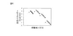
図1は、後述の特定のアミノシラン前駆体1〜6、すなわち、トリス(1,1−ジメチルヒドラジノ)−tert−ブチルシラン、ビス(1,1−ジメチルヒドラジノ)エチルシラン、ビス(1,1−ジメチルヒドラジノ)メチルシラン、ビス(ジエチルアミノ)シラン、トリス(イソ−プロピルアミノ)シラン、およびトリス(tert−ブチルアミノ)シランの各々に対して実験的に測定された堆積温度とコンピューターモデリングソフトウエアーを用いて計算した活性化バリヤーレベルとの相関のグラフ表示を示している。図1は活性化バリヤーが堆積温度と共に増加することを示す。図2はアミノシラン前駆体1〜6に対する実験的に測定した堆積温度およびコンピューターモデリングソフトウエアーを用いて計算した反応熱のグラフ表示を示している。図2は堆積温度が反応熱と共に増加することを示す。図3はアミノシラン前駆体1〜6に対する実験的に測定した活性化エネルギーとコンピューターモデリングソフトウエアーを用いて計算した反応熱の相関のグラフ表示を示している。この例は活性化バリヤーが反応熱と共に増加することを示している。図1〜図3の結果の検討により、特定の態様においては、前駆体の堆積温度は上述の式(2)を適用することによる反応熱によりコンピューター的に予測され得る。特定の態様において、アミノシラン前駆体の活性化エネルギーは約45kcal/mol以下、又は約40kcal/mol以下、又は約35kcal/mol以下、又は約30kcal/mol以下、又は約25kcal/mol以下が望ましい。この又は他の態様において、アミノシラン前駆体の反応エネルギーは約5.5kcal/mol以下、又は約4.0kcal/mol以下、又は約3.5kcal/mol以下、又は約3.0kcal/mol以下、又は約2.5kcal/mol以下が望ましい。 FIG. 1 shows
図1〜図3で用いた前駆体1〜6、すなわち、トリス(1,1−ジメチルヒドラジノ)−tert−ブチルシラン、ビス(1,1−ジメチルヒドラジン)エチルシラン、ビス(1,1−ジメチルヒドラジノ)メチルシラン、ビス(ジエチルアミノ)シラン、トリス(イソ−プロピルアミノ)シラン、およびトリス(tert−ブチルアミノ)シランの構造を以下に示す。 The
1つの態様において、式(I)又は(II)で示されるように少なくとも1つの電子吸引性置換基を有するアミノシラン前駆体はクロロシランと対応するアミンとのアミノ化反応によって製造され得る。反応に良く適した代表的なアミンはアルキル、環式、およびヘテロ環式である。好適なアミンは低級アルキル、例えばエチル、イソ−プロピル、t−ブチル、およびシクロヘキシルアミンである。さらに、アミンは望まれる生成物に依存して、1級又は2級であり得る。アミン化反応は典型的には室温以下で行われる。炭化水素溶媒、例えばヘキサンおよびペンタンが通常反応媒体として用いられる。1つの特定の態様において、式(I)又は(II)を有するアミノシラン前駆体は次の典型的な反応(A)、(B)、および(C)によって示されるように製造され得る。
R1R2NH+ClSiH3→R1R2N−SiH3+R1R2NH−HCl(A)
4R1R2NH+H2SiCl2→R1R2N−SiH2−NR1R2
+2R1R2NH−HCl(B)
6R1R2NH+HSiCl3→(R1R2N)3SiH
+3R1R2NH−HCl(C)In one embodiment, an aminosilane precursor having at least one electron withdrawing substituent as shown in formula (I) or (II) can be prepared by amination reaction of chlorosilane with the corresponding amine. Representative amines well suited for the reaction are alkyl, cyclic, and heterocyclic. Suitable amines are lower alkyls such as ethyl, iso-propyl, t-butyl, and cyclohexylamine. Furthermore, the amine can be primary or secondary depending on the desired product. The amination reaction is typically performed at room temperature or lower. Hydrocarbon solvents such as hexane and pentane are usually used as reaction media. In one particular embodiment, an aminosilane precursor having formula (I) or (II) can be prepared as shown by the following exemplary reactions (A), (B), and (C).
R1 R2 NH + ClSiH3 → R1 R2 N—SiH3 + R1 R2 NH—HCl (A)
4R1 R2 NH + H2 SiCl2 → R1 R2 N—SiH2 —NR1 R2
+ 2R1 R2 NH—HCl (B)
6R1 R2 NH + HSiCl3 → (R1 R2 N)3 SiH
+ 3R1 R2 NH—HCl (C)
他の態様において、式(I)のアミノシラン前駆体は本明細書の実施例4、5、および6に記載されている方法を用いて製造される。これら又は他の態様において、本明細書に記載されたアミノシラン前駆体はより一般的に入手可能であるアミノシランからのアミノ基転移反応により製造され得る。 In other embodiments, the aminosilane precursor of formula (I) is prepared using the methods described in Examples 4, 5, and 6 herein. In these or other embodiments, the aminosilane precursors described herein can be prepared by transamination reactions from aminosilanes that are more commonly available.
前述したように、本明細書に記載の式(I)又は(II)のアミノシラン前駆体は基材にシリコン含有膜、例えば限定されないが窒化ケイ素、酸化ケイ素、シリコンカーボナイトライド、および酸窒化ケイ素の膜の堆積用前駆体として用いられ得る。適した基材の例として、限定されないが半導体材料、例えばガリウムヒ化物(“GaAs”)、窒化ホウ素(“BN”)、シリコン、およびシリコン含有組成物、例えば結晶シリコン、ポリシリコン、アモルファスシリコン、エピタキシャルシリコン、二酸化ケイ素(“SiO2”)、炭化ケイ素(“SiC”)、シリコンオキシカーバイド(“SiOC”)、窒化ケイ素(“SiN”)、シリコンカーボナイトライド(“SiCN”)、有機ケイ酸塩ガラス(“OSG”)、有機フルオロケイ酸塩ガラス(“OFSG”)、フルオロケイ酸塩ガラス(“FSG”)、および他の適した基材又はそれらの混合物が挙げられる。基材は、さらに膜が適用される種々の層、例えば反射防止塗膜、フォトレジスト、有機ポリマー、多孔質の有機および無機材料、金属、例えば銅およびアルミニウム、又は拡散バリヤー層を含み得る。式(I)のアミノシラン前駆体は本明細書に記載の又は当業界で周知の任意の技術を用いて堆積され得る。例示的な堆積技術として、限定されないが化学蒸着(“CVD”)、原子層成長法(“ALD”)、パルスCVD、プラズマ補助化学蒸着(“PACVD”)およびプラズマ化学気相成長法(“PECD”)が挙げられる。As noted above, the aminosilane precursors of formula (I) or (II) described herein are formed from a silicon-containing film, such as, but not limited to, silicon nitride, silicon oxide, silicon carbonitride, and silicon oxynitride on a substrate. It can be used as a precursor for film deposition. Examples of suitable substrates include, but are not limited to, semiconductor materials such as gallium arsenide (“GaAs”), boron nitride (“BN”), silicon, and silicon-containing compositions such as crystalline silicon, polysilicon, amorphous silicon, epitaxial Silicon, silicon dioxide (“SiO2 ”), silicon carbide (“SiC”), silicon oxycarbide (“SiOC”), silicon nitride (“SiN”), silicon carbonitride (“SiCN”), organosilicate glass ("OSG"), organofluorosilicate glass ("OFSG"), fluorosilicate glass ("FSG"), and other suitable substrates or mixtures thereof. The substrate can further include various layers to which the film is applied, such as antireflective coatings, photoresists, organic polymers, porous organic and inorganic materials, metals such as copper and aluminum, or diffusion barrier layers. The aminosilane precursor of formula (I) may be deposited using any technique described herein or known in the art. Exemplary deposition techniques include, but are not limited to, chemical vapor deposition (“CVD”), atomic layer deposition (“ALD”), pulsed CVD, plasma assisted chemical vapor deposition (“PACVD”), and plasma enhanced chemical vapor deposition (“PECD”). )).
特定の態様において、アミノシラン前駆体はCVD又はALD技術を用いて基材に蒸着(堆積)される。特定の態様において、式(I)又は(II)のアミノシラン前駆体の堆積は、550℃以下、又は500℃以下、又は400℃以下、又は300℃以下又は200℃以下、又は100℃以下、又はこれらの端点の任意の範囲、例えば300℃〜550℃の温度で行われ得る。用いられ得る堆積技術に依存して、50mトール〜100トールの圧力が例示される。典型的なCVD堆積法において、アミノシラン前駆体はプロセス室、例えば真空室中に導入される。特定の態様において、式(I)のアミノシラン前駆体以外の他の化学反応剤がアミノシラン前駆体の導入の前、その間、および/又はその後に導入され得る。エネルギー源、例えば、熱的、プラズマ又は他の源はアミノシラン前駆体および任意的な化学反応剤にエネルギーを与え、よって、基材の少なくとも一部に膜を形成する。 In certain embodiments, the aminosilane precursor is deposited (deposited) on the substrate using CVD or ALD techniques. In certain embodiments, the deposition of the aminosilane precursor of formula (I) or (II) is 550 ° C. or lower, or 500 ° C. or lower, or 400 ° C. or lower, or 300 ° C. or lower, 200 ° C. or lower, or 100 ° C. or lower, or It can be carried out at any range of these end points, for example at a temperature of 300 ° C to 550 ° C. Depending on the deposition technique that can be used, pressures of 50 mTorr to 100 Torr are exemplified. In a typical CVD deposition method, the aminosilane precursor is introduced into a process chamber, such as a vacuum chamber. In certain embodiments, other chemical reactants other than the aminosilane precursor of formula (I) may be introduced before, during and / or after the introduction of the aminosilane precursor. An energy source, such as a thermal, plasma or other source, energizes the aminosilane precursor and optional chemical reactants, thus forming a film on at least a portion of the substrate.
原子層成長法(ALD)は第1前駆体そして、特定の態様においては第2前駆体のパルスの逐次的導入を含む。ALD法で1種より多い前駆体が用いられる態様においては、第1前駆体のパルスの逐次的導入、それに続くパージガスのパルスおよび/又はポンプ排気があり、続いて第2前駆体のパルスがあり、パージガスのパルスおよび/又はポンプ排気が続く。別々のパルスの逐次的導入は、基材表面での各前駆体よりなる単一層の交互自己限定的化学吸着をもたらしそして各サイクル毎に堆積材料からなる単一層を形成する。サイクルは望ましい厚さの膜を作り出すために必要に応じて繰り返される。ALD処理の間、基材は化学吸着を促進する温度範囲で、すなわち吸着種と下層の基材間の正常な結合を保つために十分低く、しかし前駆体の凝縮を避けるために十分に高く、そして各処理サイクルで望ましい表面反応に十分な活性化エネルギーを提供するために十分な温度範囲に保たれる。処理室温度は0℃から400℃に、又は0℃から300℃に、又は0℃から275℃に及び得る。ALD処理の間の処理室内の圧力は0.1〜1000トール、又は0.1〜15トール、又は0.1〜10トールであり得る。しかしながら、任意の特定のALD処理に対する温度および圧力は含まれる1種以上の前駆体に依存して変わり得ることが理解される。 Atomic layer deposition (ALD) involves the sequential introduction of a pulse of a first precursor and, in a particular embodiment, a second precursor. In embodiments where more than one precursor is used in the ALD method, there is a sequential introduction of a first precursor pulse, followed by a purge gas pulse and / or pump exhaust, followed by a second precursor pulse. Followed by a pulse of purge gas and / or pump exhaust. Sequential introduction of separate pulses results in alternating self-limited chemisorption of a single layer of each precursor at the substrate surface and forms a single layer of deposited material with each cycle. The cycle is repeated as necessary to create a film of the desired thickness. During the ALD process, the substrate is at a temperature range that promotes chemisorption, i.e. low enough to maintain normal bonding between the adsorbed species and the underlying substrate, but high enough to avoid condensation of the precursor, Each treatment cycle is then kept at a temperature range sufficient to provide sufficient activation energy for the desired surface reaction. The processing chamber temperature can range from 0 ° C to 400 ° C, or from 0 ° C to 300 ° C, or from 0 ° C to 275 ° C. The pressure in the process chamber during the ALD process can be 0.1 to 1000 Torr, or 0.1 to 15 Torr, or 0.1 to 10 Torr. However, it is understood that the temperature and pressure for any particular ALD process may vary depending on the one or more precursors included.
ALDの成長速度は通常のCVD法と比較して低い。ALD法の典型的な成長速度は1〜2Å/サイクルである。成長速度の増加への1つのアプローチはより高い基材温度で堆積を行うことによる。本明細書に記載のアミノシラン前駆体は比較的低い温度でシリコン含有膜を堆積可能であり、それ故に膜の成長速度を増加させ得る。 The growth rate of ALD is low as compared with the normal CVD method. A typical growth rate of the ALD method is 1-2 Å / cycle. One approach to increasing the growth rate is by performing the deposition at a higher substrate temperature. The aminosilane precursors described herein can deposit silicon-containing films at relatively low temperatures, and therefore can increase the growth rate of the film.
望ましい膜に依存して、シリコン含有膜の堆積法に通常の酸化剤が用いられ得る。代表的な酸化剤として、過酸化水素、亜酸化窒素、オゾン、および分子酸素が挙げられる。典型的には、酸化剤とアミノシラン前駆体との割合は有機アミノシラン前駆体1モルに対して酸化剤が0.1モルより大、好適には0.1〜6モルである。 Depending on the desired film, conventional oxidants can be used in the deposition of the silicon-containing film. Representative oxidizing agents include hydrogen peroxide, nitrous oxide, ozone, and molecular oxygen. Typically, the ratio of the oxidizing agent to the aminosilane precursor is such that the oxidizing agent is greater than 0.1 mole, preferably 0.1 to 6 moles per mole of the organic aminosilane precursor.
式(I)又は(II)のアミノシラン前駆体の堆積は、活性窒素源、例えばアンモニア、ヒドラジン、アルキルヒドラジン、ジアルキルヒドラジンおよびそれらの混合物の不存在下又は存在下に行われ得る。窒素源とアミノシランとのモル比は通常0:〜>10:1の範囲内と広い。上限は前駆体への希釈効果によって限定されそして希釈効果は堆積速度を大きく減じるであろう。好適な範囲は0.1〜4:1である。また、堆積による膜の形成は不活性ガス、例えば窒素およびヘリウムとともに含む他のガスを用いて又は用いないで行われ得る。対応する前駆体の希釈を達成するための製造装置による複数のガスの使用は堆積の追従性(conformality)を改良するか又は化学蒸気浸透法での浸透を改良し得る。 Deposition of the aminosilane precursor of formula (I) or (II) can be carried out in the absence or presence of an active nitrogen source such as ammonia, hydrazine, alkyl hydrazine, dialkyl hydrazine and mixtures thereof. The molar ratio of nitrogen source to aminosilane is usually as wide as 0: to> 10: 1. The upper limit is limited by the dilution effect on the precursor and the dilution effect will greatly reduce the deposition rate. The preferred range is 0.1-4: 1. Also, film formation by deposition can be performed with or without other gases including inert gases, such as nitrogen and helium. The use of multiple gases by the manufacturing equipment to achieve corresponding precursor dilution may improve deposition conformality or improve penetration with chemical vapor infiltration.
前述のように、特定の態様においては、処理室への式(I)又は(II)のアミノシラン前駆体の導入の前、その間、および/又はその後に追加の化学反応剤又は前駆体を導入し得る。化学反応剤の選択は望ましい最終的に得る膜の組成に依存し得る。典型的な化学反応剤としては、限定されないが酸化剤(すなわち、O2、NO、NO2、O3、CO、CO2等)、水、ハロゲン化物、ハロゲン含有シラン、アルキルクロロシラン、アルキルブロモシラン、又はアルキルヨードシラン、シリコンハロゲン化物錯体、例えばシリコンテトラクロライド、シリコンテトラブロマイド、又はシリコンテトラヨーダイド、又はそれらの組み合わせが挙げられる。また、上記錯体の誘導体も用いられ得ると予想される。化学反応剤は、処理室にガスとして直接供給され、反応室中へ蒸気化した液体、昇華した固体として供給されおよび/又は不活性キャリヤーガスによって反応室へ移送され得る。不活性ガスの例として、窒素、水素、アルゴン、キセノン等が挙げられる。As mentioned above, in certain embodiments, additional chemical reactants or precursors are introduced before, during, and / or after the introduction of the aminosilane precursor of formula (I) or (II) into the process chamber. obtain. The choice of the chemical reactant may depend on the desired final membrane composition. Typical chemical reactants include, but are not limited to, oxidizing agents (ie, O2 , NO, NO2 , O3 , CO, CO2 etc.), water, halides, halogen-containing silanes, alkylchlorosilanes, alkylbromosilanes. Or alkyliodosilanes, silicon halide complexes such as silicon tetrachloride, silicon tetrabromide, or silicon tetraiodide, or combinations thereof. It is also anticipated that derivatives of the above complexes may be used. The chemical reactant may be supplied directly as a gas to the processing chamber, supplied as a vaporized liquid, sublimated solid into the reaction chamber, and / or transferred to the reaction chamber by an inert carrier gas. Examples of the inert gas include nitrogen, hydrogen, argon, xenon and the like.
堆積処理を行う際に、本明細書に記載のアミノシランは膜の特性を変えるために他のシリル前駆体と混合され得る。他の前駆体の例として、ビス−tert−ブチルアミノシラン、トリス−イソープロピルアミノシラン、ビスージエチルアミノシラン、トリス−ジメチルアミノシラン、およびビス−イソープロピルアミノシランが挙げられる。 In performing the deposition process, the aminosilanes described herein can be mixed with other silyl precursors to alter the film properties. Examples of other precursors include bis-tert-butylaminosilane, tris-isopropylaminosilane, bis-diethylaminosilane, tris-dimethylaminosilane, and bis-isopropylaminosilane.
本明細書に記載の前述の膜形成の任意の方法ならびに当業界で周知の他の膜形成方法が単独で又は組み合わせて用いられ得る。 Any of the aforementioned film formation methods described herein, as well as other film formation methods well known in the art, may be used alone or in combination.
以下の実施例は本明細書に記載されたアミノシラン前駆体を説明するものであってなんら限定されるものではない。 The following examples illustrate the aminosilane precursors described herein and are not intended to be limiting in any way.
実施例1(BTBASにおける−CH3の−CF3による置換効果)
ビス(tert−ブチルアミノ)シランBTBASのt−ブチル基におけるメチル基の1つを以下の化学構造7に示すように−CF3基で逐次的に置換した。Example 1 (Substitution effect of —CH3 with —CF3 in BTBAS)
One of the methyl groups in the t-butyl group of bis (tert-butylamino) silane BTBAS was sequentially substituted with a —CF3 group as shown in
上記分子に対してのおよび置換された2又は3個のメチル基を有する類似の分子に対する反応エネルギーが前記式(2)およびカリフォルニア州サンジェゴのAccelyrs社により提供の表題がDMol3、マテリアルスタジオv.4.2.0.2の化学モデリングソフトウエアープログラムを用いて決定されそして結果を図4に示される。図4はメチル基の−CF3基への全部の置換が反応エネルギーの低減をもたらすことを示す。特に、分子内の全部のメチル基の−CF3基による全置換は反応を吸熱から発熱に変える。それ故、Si−N結合の開裂はBTBAS内におけるよりも大幅に低い温度で起りその際に低い堆積温度を可能とすると予想される。The reaction energies for the above molecules and for similar molecules with 2 or 3 substituted methyl groups are given above by the formula (2) and Accelyrs, Inc., San Diego, Calif., DMol3 , Materials Studio v. Determined using the 4.2.0.2 chemical modeling software program and the results are shown in FIG. FIG. 4 shows that all substitution of methyl groups with —CF3 groups results in a reduction in reaction energy. In particular, total substitution of all methyl groups in the molecule with —CF3 groups changes the reaction from endothermic to exothermic. Therefore, Si-N bond cleavage is expected to occur at a much lower temperature than in BTBAS, thereby allowing for lower deposition temperatures.
実施例2(BTBASにおける−CH3の−CNによる置換効果)
BTBASのt−ブチル基におけるメチル基を−CN基で逐次的に置換した。BTBASに対してのおよび−CN基で置換された1、2又は3個のメチル基を有する式(1)のアミノシラン前駆体に対しての反応エネルギーが前記式(2)およびカリフォルニア州サンジェゴのAccelyrs社により提供の表題がDMol3、マテリアルスタジオv.4.2.0.2の化学モデリングソフトウエアープログラムを用いて決定された。結果を図5に示す。置換は、当初は分子内の水素結合の形成に起因して反応エネルギーの増加をもたらす。しかしながら、全部の置換では、反応エネルギーはBTBASに対するよりも約1.6kcal/molほど低い。それ故、Si−N結合の開裂はBTBAS内におけるよりも低い温度で起ると予想される。Example 2 (Substitution effect of —CH3 with —CN in BTBAS)
The methyl group in the t-butyl group of BTBAS was sequentially replaced with a -CN group. The reaction energies for BTBAS and for aminosilane precursors of formula (1) having 1, 2 or 3 methyl groups substituted with -CN groups are the above formula (2) and Accelyrs of San Diego, CA The title provided by the company is DMol3 , Material Studio v. It was determined using the 4.2.0.2 chemical modeling software program. The results are shown in FIG. The substitution initially results in an increase in reaction energy due to the formation of intramolecular hydrogen bonds. However, for all substitutions, the reaction energy is about 1.6 kcal / mol lower than for BTBAS. Therefore, the cleavage of the Si-N bond is expected to occur at a lower temperature than in BTBAS.
実施例3(−F置換の効果)
少なくとも1種の電子吸引性置換基又はフッ素を含むアルキル基又はアリール基を有する一連のアミノシラン前駆体が、フッ素を含有しないかそれよりも水素を含有する類似のアミノシラン前駆体と比較された。表1に記載した分子に対してHのFによる置換を調べるために計算が行われ、また、表1には、本明細書に記載の式(2)およびカリフォルニア州サンジェゴのAccelyrs社により提供の表題がDMol3、マテリアルスタジオv.4.2.0.2の化学モデリングソフトウエアープログラムを用いて計算した反応熱が示されている。比較の結果を以下の表1に示す。Example 3 (Effect of -F substitution)
A series of aminosilane precursors having at least one electron-withdrawing substituent or fluorine-containing alkyl or aryl group were compared to similar aminosilane precursors containing no fluorine or more hydrogen. Calculations were performed to examine the substitution of H by F for the molecules listed in Table 1, and Table 1 includes the formula (2) described herein and provided by Accelyrs of San Diego, California. Title is DMol3 , Material Studio v. The heat of reaction calculated using the chemical modeling software program of 4.2.0.2 is shown. The results of comparison are shown in Table 1 below.
上記の結果は、HのFによる置換によってすべてのケースで反応エネルギーが低下され得ることを示している。特に、温度降下効果はα−サイトで顕著であり、次いでβ−サイトそしてその次にγ−サイトである。より高い水準の置換はより好ましい反応エネルギーを生み出す。 The above results show that the reaction energy can be reduced in all cases by substitution of H with F. In particular, the temperature drop effect is significant at α-sites, then β-sites and then γ-sites. Higher levels of substitution produce more favorable reaction energies.
実施例4a[ビス(3,3,−ジフルオロピペリジン)シランに至る3,3−ジフルオロピペリジン前駆体の調製]
磁気攪拌棒、N2パージバルブおよびゴム隔膜を備えた240mLのテフロン(登録商標)反応器にCH2Cl2(50mL)中のN−t−ブチル−3−ピペリドン(25g、0.1255mol)溶液を入れそして0℃に冷却した。この溶液に、ビス(2−メトキシエチル)アミノ硫黄トリフルオリド(41.58g、0.1882mol)を加えた。次いで、この混合物を室温とし、16時間にわたって撹拌した。次いで、混合物を250mLのガラスフラスコに注ぎ込みそして1℃の氷水25mLで処理した。有機相を分液ロートで分離した。有機溶液を15%NaOH水を用いてアルカリ性とし次いで乾燥(MgSO4)し、ろ過しそして真空で蒸発させた。残部を磁気攪拌棒および窒素注入管を備えた250mLの丸底フラスコ内で3MのHClと混合しそして60℃で90分間加熱した。混合物を15%NaOH水で中和し、ジエチルエーテル中に抽出し、水性相から分離し、乾燥(MgSO4)し、ろ過し次いで真空で蒸発させた。3,3−ジフルオロピペリジンの純生成物が40℃(0.1トール)での蒸留によって得られそしてG.C.M.S.マススペクトルで分析した。Example 4a [Preparation of 3,3-difluoropiperidine precursor leading to bis (3,3, -difluoropiperidine) silane]
A 240 mL Teflon reactor equipped with a magnetic stir bar, N2 purge valve and rubber septum was charged with a solution of Nt-butyl-3-piperidone (25 g, 0.1255 mol) in CH2 Cl2 (50 mL). And cooled to 0 ° C. To this solution was added bis (2-methoxyethyl) aminosulfur trifluoride (41.58 g, 0.1882 mol). The mixture was then brought to room temperature and stirred for 16 hours. The mixture was then poured into a 250 mL glass flask and treated with 25 mL of 1 ° C. ice water. The organic phase was separated with a separatory funnel. The organic solution was made alkaline with 15% aqueous NaOH and then dried (MgSO4 ), filtered and evaporated in vacuo. The remainder was mixed with 3M HCl in a 250 mL round bottom flask equipped with a magnetic stir bar and nitrogen inlet tube and heated at 60 ° C. for 90 minutes. The mixture was neutralized with 15% aqueous NaOH, extracted into diethyl ether, separated from the aqueous phase, dried (MgSO4 ), filtered and evaporated in vacuo. A pure product of 3,3-difluoropiperidine was obtained by distillation at 40 ° C. (0.1 torr) and G.P. C. M.M. S. Analyzed by mass spectrum.
実施例4b[アミノ基転移反応によるビス(3,3,−ジフルオロピペリジン)シランの調製]
0.1モルの3,3−ジフルオロピペリジンおよび0.1モルのビス(t−ブチルアミノ)シランの量を窒素で保護してフラスコ内で混合しそして攪拌した。毎4時間毎に、混合物はポンプで30分間100トールの真空にした。48時間後、最終の生成物ビス(3,3−ジフルオロピペリジノ)シランが118℃/10トールでの真空蒸留で得られた。Example 4b [Preparation of bis (3,3, -difluoropiperidine) silane by transamination reaction]
An amount of 0.1 mol of 3,3-difluoropiperidine and 0.1 mol of bis (t-butylamino) silane was mixed in the flask protected with nitrogen and stirred. Every 4 hours, the mixture was pumped to 100 torr vacuum for 30 minutes. After 48 hours, the final product bis (3,3-difluoropiperidino) silane was obtained by vacuum distillation at 118 ° C./10 torr.
実施例5[アミノ基転移反応によるビス[ビス(2−メトキシエチル)]アミノシランの調製]
0.1モルのビス(2−メトキシエチル)アミンおよび0.1モルのビス(t−ブチルアミノ)シランの量を窒素で保護してフラスコ内で混合しそして攪拌した。毎4時間毎に、混合物はポンプで30分間100トールの真空にした。48時間後、生成物ビス[ビス(2−メトキシエチル)アミノ]シランが54℃/10トールでの真空蒸留で得られた。Example 5 [Preparation of bis [bis (2-methoxyethyl)] aminosilane by transamination reaction]
An amount of 0.1 mol bis (2-methoxyethyl) amine and 0.1 mol bis (t-butylamino) silane was mixed in the flask protected with nitrogen and stirred. Every 4 hours, the mixture was pumped to 100 torr vacuum for 30 minutes. After 48 hours, the product bis [bis (2-methoxyethyl) amino] silane was obtained by vacuum distillation at 54 ° C./10 torr.
実施例6[アミノ基転移反応によるビス(2−メトキシエチル)アミノシランの調製]
0.1モルのビス(2−メトキシエチル)アミンおよび0.1モルのジエチルアミノシランの量を窒素で保護してフラスコ内で混合しそして攪拌した。毎4時間毎に、混合物はポンプで30分間100トールの真空にした。48時間後、生成物ビス[ビス(2−メトキシエチル)アミノ]シランが40℃/10トールでの真空蒸留で得られた。
本発明の実施態様は、次のとおりである:
[1]
次式(I):
(R1R2N)nSiR34−n (I)
(式中、置換基R1およびR2はそれぞれ独立に1〜20個の炭素原子を含むアルキル基および6〜30個の炭素原子を含むアリール基から選択され、
置換基R1およびR2の少なくとも1つはF、Cl、Br、I、CN、NO2、PO(OR)2、OR、RCOO、SO、SO2、SO2Rから選択される少なくとも1つの電子吸引性置換基を含みそして少なくとも1つの電子吸引性置換基におけるRはアルキル基又はアリール基から選択され、
R3はH、1〜20個の炭素原子を含むアルキル基、又は6〜12個の炭素原子を含むアリール基から選択され、そして
nは1〜4の範囲の数である。)
から成るシリコン含有膜を堆積させるためのアミノシラン前駆体。
[2]
R1およびR2が結合して環構造を形成している請求項1に記載のアミノシラン前駆体。
[3]
前記前駆体が、トリス(1,1−ジメチルヒドラジノ)−tert−ブチルシラン、ビス(1,1−ジメチルヒドラジン)エチルシラン、ビス(1,1−ジメチルヒドラジノ)メチルシラン、ビス(ジエチルアミノ)シラン、トリス(イソプロピルアミノ)シラン、トリス(tert−ブチルアミノ)シランおよびビス(3,3−ジフルオロピペリジン)シランから選択される請求項1に記載のアミノシラン前駆体。
[4]
トリス(1,1−ジメチルヒドラジノ)−tert−ブチルシランを含む請求項3に記載のアミノシラン前駆体。
[5]
ビス(1,1−ジメチルヒドラジン)エチルシランを含む請求項3に記載のアミノシラン前駆体。
[6]
ビス(1,1−ジメチルヒドラジノ)メチルシランを含む請求項3に記載のアミノシラン前駆体。
[7]
ビス(ジエチルアミノ)シランを含む請求項3に記載のアミノシラン前駆体。
[8]
トリス(イソ−プロピルアミノ)シランを含む請求項3に記載のアミノシラン前駆体。
[9]
トリス(tert−ブチルアミノ)シランを含む請求項3に記載のアミノシラン前駆体。
[10]
ビス(3,3−ジフルオロピペリジン)シランを含む請求項3に記載のアミノシラン前駆体。
[11]
化学蒸着によって基材にシリコン含有膜を堆積させるための方法であって、下記の工程:
処理室内に基材を提供すること、
アミノシラン前駆体を、反応させそして基材にシリコン含有膜を堆積させるのに十分な温度および圧力で処理室に導入すること、
を含み、その際にアミノシラン前駆体が次式(I):
(R1R2N)nSiR34−n (I)
(式中、置換基R1およびR2はそれぞれ独立に1〜20個の炭素原子を含むアルキル基および6〜30個の炭素原子を含むアリール基から選択され、
置換基R1およびR2の少なくとも1つはF、Cl、Br、I、CN、NO2、PO(OR)2、OR、RCOO、SO、SO2、SO2Rから選択される少なくとも1つの電子吸引性置換基を含みそして少なくとも1つの電子吸引性置換基におけるRはアルキル基又はアリール基から選択され、
R3はH、1〜20個の炭素原子を含むアルキル基、又は6〜12個の炭素原子を含むアリール基から選択され、そして
nは1〜4の範囲の数である。)
を有する、方法。
[12]
前記導入工程が、アンモニア、窒素およびヒドラジンから選択される窒素源をさらに含む請求項11に記載の方法。
[13]
前記窒素源が、アンモニア又は窒素であり且つ窒素源が窒素源:前駆体が0.1〜4:1の範囲で存在している請求項12に記載の方法。
[14]
前記温度が、約400℃〜約700℃の範囲である請求項11に記載の方法。
[15]
前記圧力が、約20mトール〜約20トールの範囲である請求項11に記載の方法。
[16]
次式(II):
AnSiR44−n (II)
(式中、Aは次の(a)〜(j)
から成るシリコン含有膜を堆積させるためのアミノシラン前駆体。
Example 6 [Preparation of bis (2-methoxyethyl) aminosilane by transamination reaction]
An amount of 0.1 mole bis (2-methoxyethyl) amine and 0.1 mole diethylaminosilane was mixed in a flask protected with nitrogen and stirred. Every 4 hours, the mixture was pumped to 100 torr vacuum for 30 minutes. After 48 hours, the product bis [bis (2-methoxyethyl) amino] silane was obtained by vacuum distillation at 40 ° C./10 torr.
Embodiments of the present invention are as follows:
[1]
Formula (I):
(R1R2N)nSiR34-n(I)
Wherein the substituents R1and R2are each independently selected from alkyl groups containing 1 to 20 carbon atoms and aryl groups containing 6 to 30 carbon atoms,
Atleast one of thesubstituents R1and R2is at least one selected from F, Cl, Br, I, CN, NO2, PO (OR)2, OR, RCOO, SO, SO2, SO2R Including an electron withdrawing substituent and R in at least one electron withdrawing substituent is selected from an alkyl group or an aryl group;
R3is selected from H, an alkyl group containing 1-20 carbon atoms, or an aryl group containing 6-12 carbon atoms, and
n is a number in the range of 1-4. )
An aminosilane precursor for depositing a silicon-containing film comprising:
[2]
The aminosilane precursor according to
[3]
The precursor is tris (1,1-dimethylhydrazino) -tert-butylsilane, bis (1,1-dimethylhydrazine) ethylsilane, bis (1,1-dimethylhydrazino) methylsilane, bis (diethylamino) silane, tris The aminosilane precursor of
[4]
The aminosilane precursor of
[5]
The aminosilane precursor of
[6]
The aminosilane precursor of
[7]
The aminosilane precursor of
[8]
4. The aminosilane precursor of
[9]
The aminosilane precursor according to
[10]
The aminosilane precursor of
[11]
A method for depositing a silicon-containing film on a substrate by chemical vapor deposition, comprising the following steps:
Providing a substrate in the processing chamber;
Introducing the aminosilane precursor into the processing chamber at a temperature and pressure sufficient to react and deposit a silicon-containing film on the substrate;
Wherein the aminosilane precursor is represented by the following formula (I):
(R1R2N)nSiR34-n(I)
Wherein the substituents R1and R2are each independently selected from alkyl groups containing 1 to 20 carbon atoms and aryl groups containing 6 to 30 carbon atoms,
Atleast one of thesubstituents R1and R2is at least one selected from F, Cl, Br, I, CN, NO2, PO (OR)2, OR, RCOO, SO, SO2, SO2R Including an electron withdrawing substituent and R in at least one electron withdrawing substituent is selected from an alkyl group or an aryl group;
R3is selected from H, an alkyl group containing 1-20 carbon atoms, or an aryl group containing 6-12 carbon atoms, and
n is a number in the range of 1-4. )
Having a method.
[12]
The method of claim 11, wherein the introducing step further comprises a nitrogen source selected from ammonia, nitrogen and hydrazine.
[13]
13. The method of claim 12, wherein the nitrogen source is ammonia or nitrogen and the nitrogen source is present in a range of 0.1-4: 1 nitrogen source: precursor.
[14]
The method of claim 11, wherein the temperature ranges from about 400 ° C. to about 700 ° C.
[15]
The method of claim 11, wherein the pressure ranges from about 20 mTorr to about 20 Torr.
[16]
Formula (II):
AnSiR44-n(II)
(In the formula, A is the following (a) to (j)
An aminosilane precursor for depositing a silicon-containing film comprising:
Claims (10)
Translated fromJapanese処理室内に基材を提供すること、
アミノシラン化合物を、反応させそして基材にシリコン含有膜を堆積させるのに十分な温度および圧力で処理室に導入すること、
を含み、その際にアミノシラン化合物が次式(I):
(R1R2N)nSiHR33−n (I)
(式中、置換基R1およびR2はそれぞれ独立に1〜20個の炭素原子を含むアルキル基および6〜30個の炭素原子を含むアリール基から選択され、
置換基R1およびR2の少なくとも1つはF、Cl、Br、I、CN、NO2、PO(OR)2、OR、RCOO、SO、SO2、SO2Rから選択される少なくとも1つの電子吸引性置換基を含みそして少なくとも1つの電子吸引性置換基におけるRはアルキル基又はアリール基から選択され、
R3はH、1〜20個の炭素原子を含むアルキル基、又は6〜12個の炭素原子を含むアリール基から選択され、そして
nは1〜3の範囲の数である。)
を有する、方法。A method for depositing a silicon-containing film on a substrate by chemical vapor deposition, comprising the following steps:
Providing a substrate in the processing chamber;
Introducing the aminosilane compound into the processing chamber at a temperature and pressure sufficient to react and deposit a silicon-containing film on the substrate;
In this case, the aminosilane compound is represented by the following formula (I):
(R1 R2 N)n SiHR33-n (I)
Wherein the substituents R1 and R2 are each independently selected from alkyl groups containing 1 to 20 carbon atoms and aryl groups containing 6 to 30 carbon atoms,
At least one of the substituents R1 and R2 is at least one selected from F, Cl, Br, I, CN, NO2 , PO (OR)2 , OR, RCOO, SO, SO2 , SO2 R Including an electron withdrawing substituent and R in at least one electron withdrawing substituent is selected from an alkyl group or an aryl group;
R3 is selected from H, an alkyl group containing 1-20 carbon atoms, or an aryl group containing 6-12 carbon atoms, and n is a number in the range of 1-3. )
Having a method.
AnSiHR43−n (II)
(式中、Aは次の(a)〜(d)及び(f)〜(j)
から成るシリコン含有膜を堆積させるためのアミノシラン化合物。Formula (II):
An SiHR43-n (II)
(In the formula, A represents the following (a) to (d) and (f) to (j)
An aminosilane compound for depositing a silicon-containing film comprising:
Applications Claiming Priority (2)
| Application Number | Priority Date | Filing Date | Title |
|---|---|---|---|
| US12/190,125 | 2008-08-12 | ||
| US12/190,125US8129555B2 (en) | 2008-08-12 | 2008-08-12 | Precursors for depositing silicon-containing films and methods for making and using same |
Related Child Applications (1)
| Application Number | Title | Priority Date | Filing Date |
|---|---|---|---|
| JP2014096335ADivisionJP2014177471A (en) | 2008-08-12 | 2014-05-07 | Precursor for silicon-containing film accumulation and its manufacturing and use method |
Publications (2)
| Publication Number | Publication Date |
|---|---|
| JP2010043081A JP2010043081A (en) | 2010-02-25 |
| JP5587572B2true JP5587572B2 (en) | 2014-09-10 |
Family
ID=41354086
Family Applications (4)
| Application Number | Title | Priority Date | Filing Date |
|---|---|---|---|
| JP2009184479AExpired - Fee RelatedJP5587572B2 (en) | 2008-08-12 | 2009-08-07 | Precursors for silicon-containing film deposition and methods of making and using the same |
| JP2014096335AWithdrawnJP2014177471A (en) | 2008-08-12 | 2014-05-07 | Precursor for silicon-containing film accumulation and its manufacturing and use method |
| JP2016078162AExpired - Fee RelatedJP6290961B2 (en) | 2008-08-12 | 2016-04-08 | Precursors for silicon-containing film deposition and methods of making and using the same |
| JP2017163063APendingJP2017210485A (en) | 2008-08-12 | 2017-08-28 | Precursors for depositing silicon-containing films and methods for production and use thereof |
Family Applications After (3)
| Application Number | Title | Priority Date | Filing Date |
|---|---|---|---|
| JP2014096335AWithdrawnJP2014177471A (en) | 2008-08-12 | 2014-05-07 | Precursor for silicon-containing film accumulation and its manufacturing and use method |
| JP2016078162AExpired - Fee RelatedJP6290961B2 (en) | 2008-08-12 | 2016-04-08 | Precursors for silicon-containing film deposition and methods of making and using the same |
| JP2017163063APendingJP2017210485A (en) | 2008-08-12 | 2017-08-28 | Precursors for depositing silicon-containing films and methods for production and use thereof |
Country Status (6)
| Country | Link |
|---|---|
| US (1) | US8129555B2 (en) |
| EP (2) | EP2644609B1 (en) |
| JP (4) | JP5587572B2 (en) |
| KR (2) | KR20100020440A (en) |
| CN (1) | CN101648964A (en) |
| TW (1) | TWI374887B (en) |
Cited By (1)
| Publication number | Priority date | Publication date | Assignee | Title |
|---|---|---|---|---|
| JP2014177471A (en)* | 2008-08-12 | 2014-09-25 | Air Products And Chemicals Inc | Precursor for silicon-containing film accumulation and its manufacturing and use method |
Families Citing this family (481)
| Publication number | Priority date | Publication date | Assignee | Title |
|---|---|---|---|---|
| US7875556B2 (en) | 2005-05-16 | 2011-01-25 | Air Products And Chemicals, Inc. | Precursors for CVD silicon carbo-nitride and silicon nitride films |
| US8357435B2 (en)* | 2008-05-09 | 2013-01-22 | Applied Materials, Inc. | Flowable dielectric equipment and processes |
| JP4638550B2 (en) | 2008-09-29 | 2011-02-23 | 東京エレクトロン株式会社 | Mask pattern forming method, fine pattern forming method, and film forming apparatus |
| US20100081293A1 (en)* | 2008-10-01 | 2010-04-01 | Applied Materials, Inc. | Methods for forming silicon nitride based film or silicon carbon based film |
| US10378106B2 (en) | 2008-11-14 | 2019-08-13 | Asm Ip Holding B.V. | Method of forming insulation film by modified PEALD |
| US8189364B2 (en) | 2008-12-17 | 2012-05-29 | Qs Semiconductor Australia Pty Ltd. | Charge retention structures and techniques for implementing charge controlled resistors in memory cells and arrays of memory |
| SG174296A1 (en)* | 2009-03-10 | 2011-10-28 | Air Liquide | Cyclic amino compounds for low-k silylation |
| US9394608B2 (en) | 2009-04-06 | 2016-07-19 | Asm America, Inc. | Semiconductor processing reactor and components thereof |
| US8511281B2 (en)* | 2009-07-10 | 2013-08-20 | Tula Technology, Inc. | Skip fire engine control |
| US8980382B2 (en)* | 2009-12-02 | 2015-03-17 | Applied Materials, Inc. | Oxygen-doping for non-carbon radical-component CVD films |
| US8741788B2 (en)* | 2009-08-06 | 2014-06-03 | Applied Materials, Inc. | Formation of silicon oxide using non-carbon flowable CVD processes |
| US8802201B2 (en) | 2009-08-14 | 2014-08-12 | Asm America, Inc. | Systems and methods for thin-film deposition of metal oxides using excited nitrogen-oxygen species |
| US20110042685A1 (en)* | 2009-08-18 | 2011-02-24 | Qs Semiconductor Australia Pty Ltd | Substrates and methods of fabricating epitaxial silicon carbide structures with sequential emphasis |
| US8449942B2 (en)* | 2009-11-12 | 2013-05-28 | Applied Materials, Inc. | Methods of curing non-carbon flowable CVD films |
| US20110159213A1 (en)* | 2009-12-30 | 2011-06-30 | Applied Materials, Inc. | Chemical vapor deposition improvements through radical-component modification |
| JP2013516763A (en) | 2009-12-30 | 2013-05-13 | アプライド マテリアルズ インコーポレイテッド | Dielectric film growth using radicals generated using a flexible nitrogen / hydrogen ratio |
| US8329262B2 (en) | 2010-01-05 | 2012-12-11 | Applied Materials, Inc. | Dielectric film formation using inert gas excitation |
| SG182336A1 (en)* | 2010-01-06 | 2012-08-30 | Applied Materials Inc | Flowable dielectric using oxide liner |
| KR101837648B1 (en) | 2010-01-07 | 2018-04-19 | 어플라이드 머티어리얼스, 인코포레이티드 | Insitu ozone cure for radicalcomponent cvd |
| US8236708B2 (en)* | 2010-03-09 | 2012-08-07 | Applied Materials, Inc. | Reduced pattern loading using bis(diethylamino)silane (C8H22N2Si) as silicon precursor |
| US20130078376A1 (en)* | 2010-04-01 | 2013-03-28 | L'air Liquide, Societe Anonyme Pour L'etude Et L'exploitation Des Procedes Georges Claude | Metal nitride containing film deposition using combination of amino-metal and halogenated metal precursors |
| US9892917B2 (en) | 2010-04-15 | 2018-02-13 | Lam Research Corporation | Plasma assisted atomic layer deposition of multi-layer films for patterning applications |
| US9373500B2 (en) | 2014-02-21 | 2016-06-21 | Lam Research Corporation | Plasma assisted atomic layer deposition titanium oxide for conformal encapsulation and gapfill applications |
| US9257274B2 (en) | 2010-04-15 | 2016-02-09 | Lam Research Corporation | Gapfill of variable aspect ratio features with a composite PEALD and PECVD method |
| US8637411B2 (en) | 2010-04-15 | 2014-01-28 | Novellus Systems, Inc. | Plasma activated conformal dielectric film deposition |
| US9997357B2 (en) | 2010-04-15 | 2018-06-12 | Lam Research Corporation | Capped ALD films for doping fin-shaped channel regions of 3-D IC transistors |
| US9285168B2 (en) | 2010-10-05 | 2016-03-15 | Applied Materials, Inc. | Module for ozone cure and post-cure moisture treatment |
| US8664127B2 (en) | 2010-10-15 | 2014-03-04 | Applied Materials, Inc. | Two silicon-containing precursors for gapfill enhancing dielectric liner |
| US10283321B2 (en) | 2011-01-18 | 2019-05-07 | Applied Materials, Inc. | Semiconductor processing system and methods using capacitively coupled plasma |
| US8450191B2 (en) | 2011-01-24 | 2013-05-28 | Applied Materials, Inc. | Polysilicon films by HDP-CVD |
| JP5624492B2 (en)* | 2011-02-10 | 2014-11-12 | 大陽日酸株式会社 | Calculation method, activation evaluation method, and selection method of activation energy of silicon-containing precursor |
| US8716154B2 (en) | 2011-03-04 | 2014-05-06 | Applied Materials, Inc. | Reduced pattern loading using silicon oxide multi-layers |
| US8647993B2 (en)* | 2011-04-11 | 2014-02-11 | Novellus Systems, Inc. | Methods for UV-assisted conformal film deposition |
| US8445078B2 (en) | 2011-04-20 | 2013-05-21 | Applied Materials, Inc. | Low temperature silicon oxide conversion |
| US8771807B2 (en) | 2011-05-24 | 2014-07-08 | Air Products And Chemicals, Inc. | Organoaminosilane precursors and methods for making and using same |
| US8466073B2 (en) | 2011-06-03 | 2013-06-18 | Applied Materials, Inc. | Capping layer for reduced outgassing |
| US9312155B2 (en) | 2011-06-06 | 2016-04-12 | Asm Japan K.K. | High-throughput semiconductor-processing apparatus equipped with multiple dual-chamber modules |
| US9070758B2 (en)* | 2011-06-20 | 2015-06-30 | Imec | CMOS compatible method for manufacturing a HEMT device and the HEMT device thereof |
| US9793148B2 (en) | 2011-06-22 | 2017-10-17 | Asm Japan K.K. | Method for positioning wafers in multiple wafer transport |
| JP2013008828A (en)* | 2011-06-24 | 2013-01-10 | Taiyo Nippon Sanso Corp | Formation method of silicon insulating film |
| US10364496B2 (en) | 2011-06-27 | 2019-07-30 | Asm Ip Holding B.V. | Dual section module having shared and unshared mass flow controllers |
| US10854498B2 (en) | 2011-07-15 | 2020-12-01 | Asm Ip Holding B.V. | Wafer-supporting device and method for producing same |
| US9404178B2 (en) | 2011-07-15 | 2016-08-02 | Applied Materials, Inc. | Surface treatment and deposition for reduced outgassing |
| US20130023129A1 (en) | 2011-07-20 | 2013-01-24 | Asm America, Inc. | Pressure transmitter for a semiconductor processing environment |
| US8617989B2 (en) | 2011-09-26 | 2013-12-31 | Applied Materials, Inc. | Liner property improvement |
| US8551891B2 (en) | 2011-10-04 | 2013-10-08 | Applied Materials, Inc. | Remote plasma burn-in |
| US9017481B1 (en) | 2011-10-28 | 2015-04-28 | Asm America, Inc. | Process feed management for semiconductor substrate processing |
| US8912101B2 (en)* | 2012-03-15 | 2014-12-16 | Asm Ip Holding B.V. | Method for forming Si-containing film using two precursors by ALD |
| US8946830B2 (en) | 2012-04-04 | 2015-02-03 | Asm Ip Holdings B.V. | Metal oxide protective layer for a semiconductor device |
| JP6242026B2 (en) | 2012-07-20 | 2017-12-06 | レール・リキード−ソシエテ・アノニム・プール・レテュード・エ・レクスプロワタシオン・デ・プロセデ・ジョルジュ・クロード | Organosilane precursor for ALD / CVD silicon-containing films |
| US9558931B2 (en) | 2012-07-27 | 2017-01-31 | Asm Ip Holding B.V. | System and method for gas-phase sulfur passivation of a semiconductor surface |
| US9659799B2 (en) | 2012-08-28 | 2017-05-23 | Asm Ip Holding B.V. | Systems and methods for dynamic semiconductor process scheduling |
| KR101380317B1 (en)* | 2012-08-31 | 2014-04-04 | 주식회사 유진테크 머티리얼즈 | Cyclic aminosilane compounds having excellent affinity towards silicon and metal atoms, preparing method thereof, and its application |
| US8889566B2 (en) | 2012-09-11 | 2014-11-18 | Applied Materials, Inc. | Low cost flowable dielectric films |
| US9021985B2 (en) | 2012-09-12 | 2015-05-05 | Asm Ip Holdings B.V. | Process gas management for an inductively-coupled plasma deposition reactor |
| US9324811B2 (en) | 2012-09-26 | 2016-04-26 | Asm Ip Holding B.V. | Structures and devices including a tensile-stressed silicon arsenic layer and methods of forming same |
| US10714315B2 (en) | 2012-10-12 | 2020-07-14 | Asm Ip Holdings B.V. | Semiconductor reaction chamber showerhead |
| JP6538300B2 (en) | 2012-11-08 | 2019-07-03 | ノベラス・システムズ・インコーポレーテッドNovellus Systems Incorporated | Method for depositing a film on a sensitive substrate |
| US9640416B2 (en) | 2012-12-26 | 2017-05-02 | Asm Ip Holding B.V. | Single-and dual-chamber module-attachable wafer-handling chamber |
| US9018108B2 (en) | 2013-01-25 | 2015-04-28 | Applied Materials, Inc. | Low shrinkage dielectric films |
| US20160376700A1 (en) | 2013-02-01 | 2016-12-29 | Asm Ip Holding B.V. | System for treatment of deposition reactor |
| US9589770B2 (en) | 2013-03-08 | 2017-03-07 | Asm Ip Holding B.V. | Method and systems for in-situ formation of intermediate reactive species |
| US9484191B2 (en) | 2013-03-08 | 2016-11-01 | Asm Ip Holding B.V. | Pulsed remote plasma method and system |
| US9564309B2 (en) | 2013-03-14 | 2017-02-07 | Asm Ip Holding B.V. | Si precursors for deposition of SiN at low temperatures |
| US9824881B2 (en) | 2013-03-14 | 2017-11-21 | Asm Ip Holding B.V. | Si precursors for deposition of SiN at low temperatures |
| KR102106885B1 (en)* | 2013-03-15 | 2020-05-06 | 삼성전자 주식회사 | Precursors for deposition of silicon dioxide film, and method for fabricating semiconductor device using the same |
| CN103938181B (en)* | 2013-05-30 | 2016-09-14 | 南京理工大学泰州科技学院 | A kind of preparation method of silica-based oxynitride film |
| US9796739B2 (en)* | 2013-06-26 | 2017-10-24 | Versum Materials Us, Llc | AZA-polysilane precursors and methods for depositing films comprising same |
| US8993054B2 (en) | 2013-07-12 | 2015-03-31 | Asm Ip Holding B.V. | Method and system to reduce outgassing in a reaction chamber |
| TW201509799A (en) | 2013-07-19 | 2015-03-16 | Air Liquide | Hexacoordinate silicon-containing precursors for ALD/CVD silicon-containing film applications |
| US9382268B1 (en) | 2013-07-19 | 2016-07-05 | American Air Liquide, Inc. | Sulfur containing organosilane precursors for ALD/CVD silicon-containing film applications |
| US9018111B2 (en) | 2013-07-22 | 2015-04-28 | Asm Ip Holding B.V. | Semiconductor reaction chamber with plasma capabilities |
| US9793115B2 (en) | 2013-08-14 | 2017-10-17 | Asm Ip Holding B.V. | Structures and devices including germanium-tin films and methods of forming same |
| US9240412B2 (en) | 2013-09-27 | 2016-01-19 | Asm Ip Holding B.V. | Semiconductor structure and device and methods of forming same using selective epitaxial process |
| US9556516B2 (en) | 2013-10-09 | 2017-01-31 | ASM IP Holding B.V | Method for forming Ti-containing film by PEALD using TDMAT or TDEAT |
| US9576790B2 (en) | 2013-10-16 | 2017-02-21 | Asm Ip Holding B.V. | Deposition of boron and carbon containing materials |
| US9543140B2 (en) | 2013-10-16 | 2017-01-10 | Asm Ip Holding B.V. | Deposition of boron and carbon containing materials |
| US20150140833A1 (en)* | 2013-11-18 | 2015-05-21 | Applied Materials, Inc. | Method of depositing a low-temperature, no-damage hdp sic-like film with high wet etch resistance |
| US10179947B2 (en) | 2013-11-26 | 2019-01-15 | Asm Ip Holding B.V. | Method for forming conformal nitrided, oxidized, or carbonized dielectric film by atomic layer deposition |
| US9401273B2 (en) | 2013-12-11 | 2016-07-26 | Asm Ip Holding B.V. | Atomic layer deposition of silicon carbon nitride based materials |
| US10683571B2 (en) | 2014-02-25 | 2020-06-16 | Asm Ip Holding B.V. | Gas supply manifold and method of supplying gases to chamber using same |
| US9447498B2 (en) | 2014-03-18 | 2016-09-20 | Asm Ip Holding B.V. | Method for performing uniform processing in gas system-sharing multiple reaction chambers |
| US10167557B2 (en) | 2014-03-18 | 2019-01-01 | Asm Ip Holding B.V. | Gas distribution system, reactor including the system, and methods of using the same |
| US11015245B2 (en) | 2014-03-19 | 2021-05-25 | Asm Ip Holding B.V. | Gas-phase reactor and system having exhaust plenum and components thereof |
| US9404587B2 (en) | 2014-04-24 | 2016-08-02 | ASM IP Holding B.V | Lockout tagout for semiconductor vacuum valve |
| US9412581B2 (en) | 2014-07-16 | 2016-08-09 | Applied Materials, Inc. | Low-K dielectric gapfill by flowable deposition |
| US10858737B2 (en) | 2014-07-28 | 2020-12-08 | Asm Ip Holding B.V. | Showerhead assembly and components thereof |
| US9543180B2 (en) | 2014-08-01 | 2017-01-10 | Asm Ip Holding B.V. | Apparatus and method for transporting wafers between wafer carrier and process tool under vacuum |
| US9890456B2 (en) | 2014-08-21 | 2018-02-13 | Asm Ip Holding B.V. | Method and system for in situ formation of gas-phase compounds |
| US9576792B2 (en) | 2014-09-17 | 2017-02-21 | Asm Ip Holding B.V. | Deposition of SiN |
| US10941490B2 (en) | 2014-10-07 | 2021-03-09 | Asm Ip Holding B.V. | Multiple temperature range susceptor, assembly, reactor and system including the susceptor, and methods of using the same |
| US9657845B2 (en) | 2014-10-07 | 2017-05-23 | Asm Ip Holding B.V. | Variable conductance gas distribution apparatus and method |
| KR102300403B1 (en) | 2014-11-19 | 2021-09-09 | 에이에스엠 아이피 홀딩 비.브이. | Method of depositing thin film |
| US9564312B2 (en) | 2014-11-24 | 2017-02-07 | Lam Research Corporation | Selective inhibition in atomic layer deposition of silicon-containing films |
| US10570513B2 (en) | 2014-12-13 | 2020-02-25 | American Air Liquide, Inc. | Organosilane precursors for ALD/CVD silicon-containing film applications and methods of using the same |
| KR102263121B1 (en) | 2014-12-22 | 2021-06-09 | 에이에스엠 아이피 홀딩 비.브이. | Semiconductor device and manufacuring method thereof |
| US10421766B2 (en)* | 2015-02-13 | 2019-09-24 | Versum Materials Us, Llc | Bisaminoalkoxysilane compounds and methods for using same to deposit silicon-containing films |
| US9478415B2 (en) | 2015-02-13 | 2016-10-25 | Asm Ip Holding B.V. | Method for forming film having low resistance and shallow junction depth |
| US10529542B2 (en) | 2015-03-11 | 2020-01-07 | Asm Ip Holdings B.V. | Cross-flow reactor and method |
| US10276355B2 (en) | 2015-03-12 | 2019-04-30 | Asm Ip Holding B.V. | Multi-zone reactor, system including the reactor, and method of using the same |
| US10566187B2 (en) | 2015-03-20 | 2020-02-18 | Lam Research Corporation | Ultrathin atomic layer deposition film accuracy thickness control |
| US11001599B2 (en) | 2015-03-23 | 2021-05-11 | Gelest Technologies, Inc. | N-alkyl substituted cyclic and oligomeric perhydridosilazanes, methods of preparation thereof, and silicon nitride films formed therefrom |
| TWI716333B (en)* | 2015-03-30 | 2021-01-11 | 法商液態空氣喬治斯克勞帝方法研究開發股份有限公司 | Catalyst dehydrogenative coupling of carbosilanes with ammonia, amnines and amidines |
| US9815858B2 (en) | 2015-06-16 | 2017-11-14 | Gelest Technologies, Inc. | Hydridosilapyrroles, hydridosilaazapyrroles, thiasilacyclopentanes, method for preparation thereof, and reaction products therefrom |
| US10458018B2 (en) | 2015-06-26 | 2019-10-29 | Asm Ip Holding B.V. | Structures including metal carbide material, devices including the structures, and methods of forming same |
| US10600673B2 (en) | 2015-07-07 | 2020-03-24 | Asm Ip Holding B.V. | Magnetic susceptor to baseplate seal |
| US10043661B2 (en) | 2015-07-13 | 2018-08-07 | Asm Ip Holding B.V. | Method for protecting layer by forming hydrocarbon-based extremely thin film |
| US9899291B2 (en) | 2015-07-13 | 2018-02-20 | Asm Ip Holding B.V. | Method for protecting layer by forming hydrocarbon-based extremely thin film |
| US10083836B2 (en) | 2015-07-24 | 2018-09-25 | Asm Ip Holding B.V. | Formation of boron-doped titanium metal films with high work function |
| US10087525B2 (en) | 2015-08-04 | 2018-10-02 | Asm Ip Holding B.V. | Variable gap hard stop design |
| US9647114B2 (en) | 2015-08-14 | 2017-05-09 | Asm Ip Holding B.V. | Methods of forming highly p-type doped germanium tin films and structures and devices including the films |
| US10410857B2 (en) | 2015-08-24 | 2019-09-10 | Asm Ip Holding B.V. | Formation of SiN thin films |
| US9711345B2 (en) | 2015-08-25 | 2017-07-18 | Asm Ip Holding B.V. | Method for forming aluminum nitride-based film by PEALD |
| US9960072B2 (en) | 2015-09-29 | 2018-05-01 | Asm Ip Holding B.V. | Variable adjustment for precise matching of multiple chamber cavity housings |
| US9909214B2 (en) | 2015-10-15 | 2018-03-06 | Asm Ip Holding B.V. | Method for depositing dielectric film in trenches by PEALD |
| US10211308B2 (en) | 2015-10-21 | 2019-02-19 | Asm Ip Holding B.V. | NbMC layers |
| US10322384B2 (en) | 2015-11-09 | 2019-06-18 | Asm Ip Holding B.V. | Counter flow mixer for process chamber |
| US9455138B1 (en) | 2015-11-10 | 2016-09-27 | Asm Ip Holding B.V. | Method for forming dielectric film in trenches by PEALD using H-containing gas |
| US9786491B2 (en) | 2015-11-12 | 2017-10-10 | Asm Ip Holding B.V. | Formation of SiOCN thin films |
| US9520284B1 (en)* | 2015-11-13 | 2016-12-13 | Varian Semiconductor Equipment Associates, Inc. | Ion beam activated directional deposition |
| US9905420B2 (en) | 2015-12-01 | 2018-02-27 | Asm Ip Holding B.V. | Methods of forming silicon germanium tin films and structures and devices including the films |
| US9607837B1 (en) | 2015-12-21 | 2017-03-28 | Asm Ip Holding B.V. | Method for forming silicon oxide cap layer for solid state diffusion process |
| KR20210028742A (en)* | 2015-12-21 | 2021-03-12 | 버슘머트리얼즈 유에스, 엘엘씨 | Compositions and methods using same for deposition of silicon-containing film |
| US9735024B2 (en) | 2015-12-28 | 2017-08-15 | Asm Ip Holding B.V. | Method of atomic layer etching using functional group-containing fluorocarbon |
| US9627221B1 (en) | 2015-12-28 | 2017-04-18 | Asm Ip Holding B.V. | Continuous process incorporating atomic layer etching |
| US11139308B2 (en) | 2015-12-29 | 2021-10-05 | Asm Ip Holding B.V. | Atomic layer deposition of III-V compounds to form V-NAND devices |
| US10283348B2 (en)* | 2016-01-20 | 2019-05-07 | Versum Materials Us, Llc | High temperature atomic layer deposition of silicon-containing films |
| US10529554B2 (en) | 2016-02-19 | 2020-01-07 | Asm Ip Holding B.V. | Method for forming silicon nitride film selectively on sidewalls or flat surfaces of trenches |
| US9754779B1 (en) | 2016-02-19 | 2017-09-05 | Asm Ip Holding B.V. | Method for forming silicon nitride film selectively on sidewalls or flat surfaces of trenches |
| US10468251B2 (en) | 2016-02-19 | 2019-11-05 | Asm Ip Holding B.V. | Method for forming spacers using silicon nitride film for spacer-defined multiple patterning |
| US10501866B2 (en) | 2016-03-09 | 2019-12-10 | Asm Ip Holding B.V. | Gas distribution apparatus for improved film uniformity in an epitaxial system |
| US10343920B2 (en) | 2016-03-18 | 2019-07-09 | Asm Ip Holding B.V. | Aligned carbon nanotubes |
| US9892913B2 (en) | 2016-03-24 | 2018-02-13 | Asm Ip Holding B.V. | Radial and thickness control via biased multi-port injection settings |
| US10190213B2 (en) | 2016-04-21 | 2019-01-29 | Asm Ip Holding B.V. | Deposition of metal borides |
| US10865475B2 (en) | 2016-04-21 | 2020-12-15 | Asm Ip Holding B.V. | Deposition of metal borides and silicides |
| US10087522B2 (en) | 2016-04-21 | 2018-10-02 | Asm Ip Holding B.V. | Deposition of metal borides |
| US10367080B2 (en) | 2016-05-02 | 2019-07-30 | Asm Ip Holding B.V. | Method of forming a germanium oxynitride film |
| US10032628B2 (en) | 2016-05-02 | 2018-07-24 | Asm Ip Holding B.V. | Source/drain performance through conformal solid state doping |
| KR102378021B1 (en)* | 2016-05-06 | 2022-03-23 | 에이에스엠 아이피 홀딩 비.브이. | Formation of SiOC thin films |
| KR102592471B1 (en) | 2016-05-17 | 2023-10-20 | 에이에스엠 아이피 홀딩 비.브이. | Method of forming metal interconnection and method of fabricating semiconductor device using the same |
| US11453943B2 (en) | 2016-05-25 | 2022-09-27 | Asm Ip Holding B.V. | Method for forming carbon-containing silicon/metal oxide or nitride film by ALD using silicon precursor and hydrocarbon precursor |
| US10388509B2 (en) | 2016-06-28 | 2019-08-20 | Asm Ip Holding B.V. | Formation of epitaxial layers via dislocation filtering |
| US9773643B1 (en) | 2016-06-30 | 2017-09-26 | Lam Research Corporation | Apparatus and method for deposition and etch in gap fill |
| US10062563B2 (en) | 2016-07-01 | 2018-08-28 | Lam Research Corporation | Selective atomic layer deposition with post-dose treatment |
| US10612137B2 (en) | 2016-07-08 | 2020-04-07 | Asm Ip Holdings B.V. | Organic reactants for atomic layer deposition |
| US9859151B1 (en) | 2016-07-08 | 2018-01-02 | Asm Ip Holding B.V. | Selective film deposition method to form air gaps |
| US9793135B1 (en) | 2016-07-14 | 2017-10-17 | ASM IP Holding B.V | Method of cyclic dry etching using etchant film |
| US10714385B2 (en) | 2016-07-19 | 2020-07-14 | Asm Ip Holding B.V. | Selective deposition of tungsten |
| KR102354490B1 (en) | 2016-07-27 | 2022-01-21 | 에이에스엠 아이피 홀딩 비.브이. | Method of processing a substrate |
| KR102532607B1 (en) | 2016-07-28 | 2023-05-15 | 에이에스엠 아이피 홀딩 비.브이. | Substrate processing apparatus and method of operating the same |
| US9887082B1 (en) | 2016-07-28 | 2018-02-06 | Asm Ip Holding B.V. | Method and apparatus for filling a gap |
| US9812320B1 (en) | 2016-07-28 | 2017-11-07 | Asm Ip Holding B.V. | Method and apparatus for filling a gap |
| US10177025B2 (en) | 2016-07-28 | 2019-01-08 | Asm Ip Holding B.V. | Method and apparatus for filling a gap |
| US10395919B2 (en) | 2016-07-28 | 2019-08-27 | Asm Ip Holding B.V. | Method and apparatus for filling a gap |
| US10037884B2 (en) | 2016-08-31 | 2018-07-31 | Lam Research Corporation | Selective atomic layer deposition for gapfill using sacrificial underlayer |
| US10090316B2 (en) | 2016-09-01 | 2018-10-02 | Asm Ip Holding B.V. | 3D stacked multilayer semiconductor memory using doped select transistor channel |
| US10410943B2 (en) | 2016-10-13 | 2019-09-10 | Asm Ip Holding B.V. | Method for passivating a surface of a semiconductor and related systems |
| US10643826B2 (en) | 2016-10-26 | 2020-05-05 | Asm Ip Holdings B.V. | Methods for thermally calibrating reaction chambers |
| US11532757B2 (en) | 2016-10-27 | 2022-12-20 | Asm Ip Holding B.V. | Deposition of charge trapping layers |
| US10435790B2 (en) | 2016-11-01 | 2019-10-08 | Asm Ip Holding B.V. | Method of subatmospheric plasma-enhanced ALD using capacitively coupled electrodes with narrow gap |
| US10714350B2 (en) | 2016-11-01 | 2020-07-14 | ASM IP Holdings, B.V. | Methods for forming a transition metal niobium nitride film on a substrate by atomic layer deposition and related semiconductor device structures |
| US10229833B2 (en) | 2016-11-01 | 2019-03-12 | Asm Ip Holding B.V. | Methods for forming a transition metal nitride film on a substrate by atomic layer deposition and related semiconductor device structures |
| US10643904B2 (en) | 2016-11-01 | 2020-05-05 | Asm Ip Holdings B.V. | Methods for forming a semiconductor device and related semiconductor device structures |
| US10134757B2 (en) | 2016-11-07 | 2018-11-20 | Asm Ip Holding B.V. | Method of processing a substrate and a device manufactured by using the method |
| KR102546317B1 (en) | 2016-11-15 | 2023-06-21 | 에이에스엠 아이피 홀딩 비.브이. | Gas supply unit and substrate processing apparatus including the same |
| US10340135B2 (en) | 2016-11-28 | 2019-07-02 | Asm Ip Holding B.V. | Method of topologically restricted plasma-enhanced cyclic deposition of silicon or metal nitride |
| KR102762543B1 (en) | 2016-12-14 | 2025-02-05 | 에이에스엠 아이피 홀딩 비.브이. | Substrate processing apparatus |
| US11581186B2 (en) | 2016-12-15 | 2023-02-14 | Asm Ip Holding B.V. | Sequential infiltration synthesis apparatus |
| US11447861B2 (en) | 2016-12-15 | 2022-09-20 | Asm Ip Holding B.V. | Sequential infiltration synthesis apparatus and a method of forming a patterned structure |
| US9916980B1 (en) | 2016-12-15 | 2018-03-13 | Asm Ip Holding B.V. | Method of forming a structure on a substrate |
| KR102700194B1 (en) | 2016-12-19 | 2024-08-28 | 에이에스엠 아이피 홀딩 비.브이. | Substrate processing apparatus |
| US10269558B2 (en) | 2016-12-22 | 2019-04-23 | Asm Ip Holding B.V. | Method of forming a structure on a substrate |
| US10867788B2 (en) | 2016-12-28 | 2020-12-15 | Asm Ip Holding B.V. | Method of forming a structure on a substrate |
| US11390950B2 (en) | 2017-01-10 | 2022-07-19 | Asm Ip Holding B.V. | Reactor system and method to reduce residue buildup during a film deposition process |
| US10655221B2 (en) | 2017-02-09 | 2020-05-19 | Asm Ip Holding B.V. | Method for depositing oxide film by thermal ALD and PEALD |
| US10176984B2 (en)* | 2017-02-14 | 2019-01-08 | Lam Research Corporation | Selective deposition of silicon oxide |
| US10468261B2 (en) | 2017-02-15 | 2019-11-05 | Asm Ip Holding B.V. | Methods for forming a metallic film on a substrate by cyclical deposition and related semiconductor device structures |
| JP6812855B2 (en)* | 2017-03-10 | 2021-01-13 | Jnc株式会社 | Method for producing dialkylaminosilane |
| US10529563B2 (en) | 2017-03-29 | 2020-01-07 | Asm Ip Holdings B.V. | Method for forming doped metal oxide films on a substrate by cyclical deposition and related semiconductor device structures |
| US10283353B2 (en) | 2017-03-29 | 2019-05-07 | Asm Ip Holding B.V. | Method of reforming insulating film deposited on substrate with recess pattern |
| US10103040B1 (en) | 2017-03-31 | 2018-10-16 | Asm Ip Holding B.V. | Apparatus and method for manufacturing a semiconductor device |
| USD830981S1 (en) | 2017-04-07 | 2018-10-16 | Asm Ip Holding B.V. | Susceptor for semiconductor substrate processing apparatus |
| KR102457289B1 (en) | 2017-04-25 | 2022-10-21 | 에이에스엠 아이피 홀딩 비.브이. | Method for depositing a thin film and manufacturing a semiconductor device |
| CN114875388A (en) | 2017-05-05 | 2022-08-09 | Asm Ip 控股有限公司 | Plasma enhanced deposition method for controlled formation of oxygen-containing films |
| US10770286B2 (en) | 2017-05-08 | 2020-09-08 | Asm Ip Holdings B.V. | Methods for selectively forming a silicon nitride film on a substrate and related semiconductor device structures |
| US10892156B2 (en) | 2017-05-08 | 2021-01-12 | Asm Ip Holding B.V. | Methods for forming a silicon nitride film on a substrate and related semiconductor device structures |
| US10446393B2 (en) | 2017-05-08 | 2019-10-15 | Asm Ip Holding B.V. | Methods for forming silicon-containing epitaxial layers and related semiconductor device structures |
| US10504742B2 (en) | 2017-05-31 | 2019-12-10 | Asm Ip Holding B.V. | Method of atomic layer etching using hydrogen plasma |
| US11056353B2 (en) | 2017-06-01 | 2021-07-06 | Asm Ip Holding B.V. | Method and structure for wet etch utilizing etch protection layer comprising boron and carbon |
| US10886123B2 (en) | 2017-06-02 | 2021-01-05 | Asm Ip Holding B.V. | Methods for forming low temperature semiconductor layers and related semiconductor device structures |
| US12040200B2 (en) | 2017-06-20 | 2024-07-16 | Asm Ip Holding B.V. | Semiconductor processing apparatus and methods for calibrating a semiconductor processing apparatus |
| US11306395B2 (en) | 2017-06-28 | 2022-04-19 | Asm Ip Holding B.V. | Methods for depositing a transition metal nitride film on a substrate by atomic layer deposition and related deposition apparatus |
| US10685834B2 (en) | 2017-07-05 | 2020-06-16 | Asm Ip Holdings B.V. | Methods for forming a silicon germanium tin layer and related semiconductor device structures |
| KR20190009245A (en) | 2017-07-18 | 2019-01-28 | 에이에스엠 아이피 홀딩 비.브이. | Methods for forming a semiconductor device structure and related semiconductor device structures |
| US11018002B2 (en) | 2017-07-19 | 2021-05-25 | Asm Ip Holding B.V. | Method for selectively depositing a Group IV semiconductor and related semiconductor device structures |
| US10541333B2 (en) | 2017-07-19 | 2020-01-21 | Asm Ip Holding B.V. | Method for depositing a group IV semiconductor and related semiconductor device structures |
| US11374112B2 (en) | 2017-07-19 | 2022-06-28 | Asm Ip Holding B.V. | Method for depositing a group IV semiconductor and related semiconductor device structures |
| US10605530B2 (en) | 2017-07-26 | 2020-03-31 | Asm Ip Holding B.V. | Assembly of a liner and a flange for a vertical furnace as well as the liner and the vertical furnace |
| US10590535B2 (en) | 2017-07-26 | 2020-03-17 | Asm Ip Holdings B.V. | Chemical treatment, deposition and/or infiltration apparatus and method for using the same |
| US10312055B2 (en) | 2017-07-26 | 2019-06-04 | Asm Ip Holding B.V. | Method of depositing film by PEALD using negative bias |
| TWI815813B (en) | 2017-08-04 | 2023-09-21 | 荷蘭商Asm智慧財產控股公司 | Showerhead assembly for distributing a gas within a reaction chamber |
| US10692741B2 (en) | 2017-08-08 | 2020-06-23 | Asm Ip Holdings B.V. | Radiation shield |
| US10770336B2 (en) | 2017-08-08 | 2020-09-08 | Asm Ip Holding B.V. | Substrate lift mechanism and reactor including same |
| US10249524B2 (en) | 2017-08-09 | 2019-04-02 | Asm Ip Holding B.V. | Cassette holder assembly for a substrate cassette and holding member for use in such assembly |
| US11769682B2 (en) | 2017-08-09 | 2023-09-26 | Asm Ip Holding B.V. | Storage apparatus for storing cassettes for substrates and processing apparatus equipped therewith |
| US11139191B2 (en) | 2017-08-09 | 2021-10-05 | Asm Ip Holding B.V. | Storage apparatus for storing cassettes for substrates and processing apparatus equipped therewith |
| US10236177B1 (en) | 2017-08-22 | 2019-03-19 | ASM IP Holding B.V.. | Methods for depositing a doped germanium tin semiconductor and related semiconductor device structures |
| USD900036S1 (en) | 2017-08-24 | 2020-10-27 | Asm Ip Holding B.V. | Heater electrical connector and adapter |
| US11830730B2 (en) | 2017-08-29 | 2023-11-28 | Asm Ip Holding B.V. | Layer forming method and apparatus |
| KR102491945B1 (en) | 2017-08-30 | 2023-01-26 | 에이에스엠 아이피 홀딩 비.브이. | Substrate processing apparatus |
| US11295980B2 (en) | 2017-08-30 | 2022-04-05 | Asm Ip Holding B.V. | Methods for depositing a molybdenum metal film over a dielectric surface of a substrate by a cyclical deposition process and related semiconductor device structures |
| US11056344B2 (en) | 2017-08-30 | 2021-07-06 | Asm Ip Holding B.V. | Layer forming method |
| KR102401446B1 (en) | 2017-08-31 | 2022-05-24 | 에이에스엠 아이피 홀딩 비.브이. | Substrate processing apparatus |
| US10269559B2 (en) | 2017-09-13 | 2019-04-23 | Lam Research Corporation | Dielectric gapfill of high aspect ratio features utilizing a sacrificial etch cap layer |
| US10607895B2 (en) | 2017-09-18 | 2020-03-31 | Asm Ip Holdings B.V. | Method for forming a semiconductor device structure comprising a gate fill metal |
| KR102630301B1 (en) | 2017-09-21 | 2024-01-29 | 에이에스엠 아이피 홀딩 비.브이. | Method of sequential infiltration synthesis treatment of infiltrateable material and structures and devices formed using same |
| US10844484B2 (en) | 2017-09-22 | 2020-11-24 | Asm Ip Holding B.V. | Apparatus for dispensing a vapor phase reactant to a reaction chamber and related methods |
| US10658205B2 (en) | 2017-09-28 | 2020-05-19 | Asm Ip Holdings B.V. | Chemical dispensing apparatus and methods for dispensing a chemical to a reaction chamber |
| US10403504B2 (en) | 2017-10-05 | 2019-09-03 | Asm Ip Holding B.V. | Method for selectively depositing a metallic film on a substrate |
| US10319588B2 (en) | 2017-10-10 | 2019-06-11 | Asm Ip Holding B.V. | Method for depositing a metal chalcogenide on a substrate by cyclical deposition |
| US10923344B2 (en) | 2017-10-30 | 2021-02-16 | Asm Ip Holding B.V. | Methods for forming a semiconductor structure and related semiconductor structures |
| US10910262B2 (en) | 2017-11-16 | 2021-02-02 | Asm Ip Holding B.V. | Method of selectively depositing a capping layer structure on a semiconductor device structure |
| KR102443047B1 (en) | 2017-11-16 | 2022-09-14 | 에이에스엠 아이피 홀딩 비.브이. | Method of processing a substrate and a device manufactured by the same |
| US11022879B2 (en) | 2017-11-24 | 2021-06-01 | Asm Ip Holding B.V. | Method of forming an enhanced unexposed photoresist layer |
| CN111344522B (en) | 2017-11-27 | 2022-04-12 | 阿斯莫Ip控股公司 | Including clean mini-environment device |
| WO2019103613A1 (en) | 2017-11-27 | 2019-05-31 | Asm Ip Holding B.V. | A storage device for storing wafer cassettes for use with a batch furnace |
| US10290508B1 (en) | 2017-12-05 | 2019-05-14 | Asm Ip Holding B.V. | Method for forming vertical spacers for spacer-defined patterning |
| US10872771B2 (en) | 2018-01-16 | 2020-12-22 | Asm Ip Holding B. V. | Method for depositing a material film on a substrate within a reaction chamber by a cyclical deposition process and related device structures |
| KR102695659B1 (en) | 2018-01-19 | 2024-08-14 | 에이에스엠 아이피 홀딩 비.브이. | Method for depositing a gap filling layer by plasma assisted deposition |
| TWI799494B (en) | 2018-01-19 | 2023-04-21 | 荷蘭商Asm 智慧財產控股公司 | Deposition method |
| USD903477S1 (en) | 2018-01-24 | 2020-12-01 | Asm Ip Holdings B.V. | Metal clamp |
| US11018047B2 (en) | 2018-01-25 | 2021-05-25 | Asm Ip Holding B.V. | Hybrid lift pin |
| US10535516B2 (en) | 2018-02-01 | 2020-01-14 | Asm Ip Holdings B.V. | Method for depositing a semiconductor structure on a surface of a substrate and related semiconductor structures |
| USD880437S1 (en) | 2018-02-01 | 2020-04-07 | Asm Ip Holding B.V. | Gas supply plate for semiconductor manufacturing apparatus |
| US11081345B2 (en) | 2018-02-06 | 2021-08-03 | Asm Ip Holding B.V. | Method of post-deposition treatment for silicon oxide film |
| WO2019158960A1 (en) | 2018-02-14 | 2019-08-22 | Asm Ip Holding B.V. | A method for depositing a ruthenium-containing film on a substrate by a cyclical deposition process |
| US10896820B2 (en) | 2018-02-14 | 2021-01-19 | Asm Ip Holding B.V. | Method for depositing a ruthenium-containing film on a substrate by a cyclical deposition process |
| US10731249B2 (en) | 2018-02-15 | 2020-08-04 | Asm Ip Holding B.V. | Method of forming a transition metal containing film on a substrate by a cyclical deposition process, a method for supplying a transition metal halide compound to a reaction chamber, and related vapor deposition apparatus |
| KR102636427B1 (en) | 2018-02-20 | 2024-02-13 | 에이에스엠 아이피 홀딩 비.브이. | Substrate processing method and apparatus |
| US10658181B2 (en) | 2018-02-20 | 2020-05-19 | Asm Ip Holding B.V. | Method of spacer-defined direct patterning in semiconductor fabrication |
| US10975470B2 (en) | 2018-02-23 | 2021-04-13 | Asm Ip Holding B.V. | Apparatus for detecting or monitoring for a chemical precursor in a high temperature environment |
| US11473195B2 (en) | 2018-03-01 | 2022-10-18 | Asm Ip Holding B.V. | Semiconductor processing apparatus and a method for processing a substrate |
| CN112005343B (en) | 2018-03-02 | 2025-05-06 | 朗姆研究公司 | Selective deposition using hydrolysis |
| US11629406B2 (en) | 2018-03-09 | 2023-04-18 | Asm Ip Holding B.V. | Semiconductor processing apparatus comprising one or more pyrometers for measuring a temperature of a substrate during transfer of the substrate |
| US11114283B2 (en) | 2018-03-16 | 2021-09-07 | Asm Ip Holding B.V. | Reactor, system including the reactor, and methods of manufacturing and using same |
| KR102646467B1 (en) | 2018-03-27 | 2024-03-11 | 에이에스엠 아이피 홀딩 비.브이. | Method of forming an electrode on a substrate and a semiconductor device structure including an electrode |
| US11230766B2 (en) | 2018-03-29 | 2022-01-25 | Asm Ip Holding B.V. | Substrate processing apparatus and method |
| US11088002B2 (en) | 2018-03-29 | 2021-08-10 | Asm Ip Holding B.V. | Substrate rack and a substrate processing system and method |
| US10510536B2 (en) | 2018-03-29 | 2019-12-17 | Asm Ip Holding B.V. | Method of depositing a co-doped polysilicon film on a surface of a substrate within a reaction chamber |
| KR102501472B1 (en) | 2018-03-30 | 2023-02-20 | 에이에스엠 아이피 홀딩 비.브이. | Substrate processing method |
| KR102173384B1 (en)* | 2018-03-30 | 2020-11-03 | 에스케이트리켐 주식회사 | PRECURSOR FOR SiO2 THIN FILM, DEPOSITION METHOD OF SiO2 THIN FILM USING THE SAME |
| KR102600229B1 (en) | 2018-04-09 | 2023-11-10 | 에이에스엠 아이피 홀딩 비.브이. | Substrate supporting device, substrate processing apparatus including the same and substrate processing method |
| US10580645B2 (en) | 2018-04-30 | 2020-03-03 | Asm Ip Holding B.V. | Plasma enhanced atomic layer deposition (PEALD) of SiN using silicon-hydrohalide precursors |
| TWI811348B (en) | 2018-05-08 | 2023-08-11 | 荷蘭商Asm 智慧財產控股公司 | Methods for depositing an oxide film on a substrate by a cyclical deposition process and related device structures |
| US12025484B2 (en) | 2018-05-08 | 2024-07-02 | Asm Ip Holding B.V. | Thin film forming method |
| US12272527B2 (en) | 2018-05-09 | 2025-04-08 | Asm Ip Holding B.V. | Apparatus for use with hydrogen radicals and method of using same |
| KR20190129718A (en) | 2018-05-11 | 2019-11-20 | 에이에스엠 아이피 홀딩 비.브이. | Methods for forming a doped metal carbide film on a substrate and related semiconductor device structures |
| KR102596988B1 (en) | 2018-05-28 | 2023-10-31 | 에이에스엠 아이피 홀딩 비.브이. | Method of processing a substrate and a device manufactured by the same |
| TWI840362B (en) | 2018-06-04 | 2024-05-01 | 荷蘭商Asm Ip私人控股有限公司 | Wafer handling chamber with moisture reduction |
| US11718913B2 (en) | 2018-06-04 | 2023-08-08 | Asm Ip Holding B.V. | Gas distribution system and reactor system including same |
| US11286562B2 (en) | 2018-06-08 | 2022-03-29 | Asm Ip Holding B.V. | Gas-phase chemical reactor and method of using same |
| KR102568797B1 (en) | 2018-06-21 | 2023-08-21 | 에이에스엠 아이피 홀딩 비.브이. | Substrate processing system |
| US10797133B2 (en) | 2018-06-21 | 2020-10-06 | Asm Ip Holding B.V. | Method for depositing a phosphorus doped silicon arsenide film and related semiconductor device structures |
| KR102854019B1 (en) | 2018-06-27 | 2025-09-02 | 에이에스엠 아이피 홀딩 비.브이. | Periodic deposition method for forming a metal-containing material and films and structures comprising the metal-containing material |
| TWI873894B (en) | 2018-06-27 | 2025-02-21 | 荷蘭商Asm Ip私人控股有限公司 | Cyclic deposition methods for forming metal-containing material and films and structures including the metal-containing material |
| KR102686758B1 (en) | 2018-06-29 | 2024-07-18 | 에이에스엠 아이피 홀딩 비.브이. | Method for depositing a thin film and manufacturing a semiconductor device |
| US10612136B2 (en) | 2018-06-29 | 2020-04-07 | ASM IP Holding, B.V. | Temperature-controlled flange and reactor system including same |
| US10388513B1 (en) | 2018-07-03 | 2019-08-20 | Asm Ip Holding B.V. | Method for depositing silicon-free carbon-containing film as gap-fill layer by pulse plasma-assisted deposition |
| US10755922B2 (en) | 2018-07-03 | 2020-08-25 | Asm Ip Holding B.V. | Method for depositing silicon-free carbon-containing film as gap-fill layer by pulse plasma-assisted deposition |
| WO2020014631A1 (en)* | 2018-07-12 | 2020-01-16 | Lotus Applied Technology, Llc | Water-insensitive methods of forming metal oxide films and products related thereto |
| US10767789B2 (en) | 2018-07-16 | 2020-09-08 | Asm Ip Holding B.V. | Diaphragm valves, valve components, and methods for forming valve components |
| US10483099B1 (en) | 2018-07-26 | 2019-11-19 | Asm Ip Holding B.V. | Method for forming thermally stable organosilicon polymer film |
| US11053591B2 (en) | 2018-08-06 | 2021-07-06 | Asm Ip Holding B.V. | Multi-port gas injection system and reactor system including same |
| US10883175B2 (en) | 2018-08-09 | 2021-01-05 | Asm Ip Holding B.V. | Vertical furnace for processing substrates and a liner for use therein |
| US10829852B2 (en) | 2018-08-16 | 2020-11-10 | Asm Ip Holding B.V. | Gas distribution device for a wafer processing apparatus |
| US11430674B2 (en) | 2018-08-22 | 2022-08-30 | Asm Ip Holding B.V. | Sensor array, apparatus for dispensing a vapor phase reactant to a reaction chamber and related methods |
| KR102707956B1 (en) | 2018-09-11 | 2024-09-19 | 에이에스엠 아이피 홀딩 비.브이. | Method for deposition of a thin film |
| US11024523B2 (en) | 2018-09-11 | 2021-06-01 | Asm Ip Holding B.V. | Substrate processing apparatus and method |
| US11049751B2 (en) | 2018-09-14 | 2021-06-29 | Asm Ip Holding B.V. | Cassette supply system to store and handle cassettes and processing apparatus equipped therewith |
| CN110970344B (en) | 2018-10-01 | 2024-10-25 | Asmip控股有限公司 | Substrate holding apparatus, system comprising the same and method of using the same |
| US11232963B2 (en) | 2018-10-03 | 2022-01-25 | Asm Ip Holding B.V. | Substrate processing apparatus and method |
| KR102592699B1 (en) | 2018-10-08 | 2023-10-23 | 에이에스엠 아이피 홀딩 비.브이. | Substrate support unit and apparatuses for depositing thin film and processing the substrate including the same |
| US10847365B2 (en) | 2018-10-11 | 2020-11-24 | Asm Ip Holding B.V. | Method of forming conformal silicon carbide film by cyclic CVD |
| US10811256B2 (en) | 2018-10-16 | 2020-10-20 | Asm Ip Holding B.V. | Method for etching a carbon-containing feature |
| KR102605121B1 (en) | 2018-10-19 | 2023-11-23 | 에이에스엠 아이피 홀딩 비.브이. | Substrate processing apparatus and substrate processing method |
| KR102546322B1 (en) | 2018-10-19 | 2023-06-21 | 에이에스엠 아이피 홀딩 비.브이. | Substrate processing apparatus and substrate processing method |
| USD948463S1 (en) | 2018-10-24 | 2022-04-12 | Asm Ip Holding B.V. | Susceptor for semiconductor substrate supporting apparatus |
| US10381219B1 (en) | 2018-10-25 | 2019-08-13 | Asm Ip Holding B.V. | Methods for forming a silicon nitride film |
| US12378665B2 (en) | 2018-10-26 | 2025-08-05 | Asm Ip Holding B.V. | High temperature coatings for a preclean and etch apparatus and related methods |
| US11087997B2 (en) | 2018-10-31 | 2021-08-10 | Asm Ip Holding B.V. | Substrate processing apparatus for processing substrates |
| KR102748291B1 (en) | 2018-11-02 | 2024-12-31 | 에이에스엠 아이피 홀딩 비.브이. | Substrate support unit and substrate processing apparatus including the same |
| US11572620B2 (en) | 2018-11-06 | 2023-02-07 | Asm Ip Holding B.V. | Methods for selectively depositing an amorphous silicon film on a substrate |
| US11031242B2 (en) | 2018-11-07 | 2021-06-08 | Asm Ip Holding B.V. | Methods for depositing a boron doped silicon germanium film |
| US10847366B2 (en) | 2018-11-16 | 2020-11-24 | Asm Ip Holding B.V. | Methods for depositing a transition metal chalcogenide film on a substrate by a cyclical deposition process |
| US10818758B2 (en) | 2018-11-16 | 2020-10-27 | Asm Ip Holding B.V. | Methods for forming a metal silicate film on a substrate in a reaction chamber and related semiconductor device structures |
| US10559458B1 (en) | 2018-11-26 | 2020-02-11 | Asm Ip Holding B.V. | Method of forming oxynitride film |
| US12040199B2 (en) | 2018-11-28 | 2024-07-16 | Asm Ip Holding B.V. | Substrate processing apparatus for processing substrates |
| US11217444B2 (en) | 2018-11-30 | 2022-01-04 | Asm Ip Holding B.V. | Method for forming an ultraviolet radiation responsive metal oxide-containing film |
| KR102157137B1 (en)* | 2018-11-30 | 2020-09-17 | 주식회사 한솔케미칼 | Silicon precursor and fabrication method of silicon-containing thin film using the same |
| KR102636428B1 (en) | 2018-12-04 | 2024-02-13 | 에이에스엠 아이피 홀딩 비.브이. | A method for cleaning a substrate processing apparatus |
| US11158513B2 (en) | 2018-12-13 | 2021-10-26 | Asm Ip Holding B.V. | Methods for forming a rhenium-containing film on a substrate by a cyclical deposition process and related semiconductor device structures |
| TWI874340B (en) | 2018-12-14 | 2025-03-01 | 荷蘭商Asm Ip私人控股有限公司 | Method of forming device structure, structure formed by the method and system for performing the method |
| TWI866480B (en) | 2019-01-17 | 2024-12-11 | 荷蘭商Asm Ip 私人控股有限公司 | Methods of forming a transition metal containing film on a substrate by a cyclical deposition process |
| KR102727227B1 (en) | 2019-01-22 | 2024-11-07 | 에이에스엠 아이피 홀딩 비.브이. | Semiconductor processing device |
| CN111524788B (en) | 2019-02-01 | 2023-11-24 | Asm Ip私人控股有限公司 | Method for forming topologically selective films of silicon oxide |
| TWI873122B (en) | 2019-02-20 | 2025-02-21 | 荷蘭商Asm Ip私人控股有限公司 | Method of filling a recess formed within a surface of a substrate, semiconductor structure formed according to the method, and semiconductor processing apparatus |
| TWI845607B (en) | 2019-02-20 | 2024-06-21 | 荷蘭商Asm Ip私人控股有限公司 | Cyclical deposition method and apparatus for filling a recess formed within a substrate surface |
| KR102626263B1 (en) | 2019-02-20 | 2024-01-16 | 에이에스엠 아이피 홀딩 비.브이. | Cyclical deposition method including treatment step and apparatus for same |
| TWI838458B (en) | 2019-02-20 | 2024-04-11 | 荷蘭商Asm Ip私人控股有限公司 | Apparatus and methods for plug fill deposition in 3-d nand applications |
| TWI842826B (en) | 2019-02-22 | 2024-05-21 | 荷蘭商Asm Ip私人控股有限公司 | Substrate processing apparatus and method for processing substrate |
| KR102858005B1 (en) | 2019-03-08 | 2025-09-09 | 에이에스엠 아이피 홀딩 비.브이. | Method for Selective Deposition of Silicon Nitride Layer and Structure Including Selectively-Deposited Silicon Nitride Layer |
| US11742198B2 (en) | 2019-03-08 | 2023-08-29 | Asm Ip Holding B.V. | Structure including SiOCN layer and method of forming same |
| KR102782593B1 (en) | 2019-03-08 | 2025-03-14 | 에이에스엠 아이피 홀딩 비.브이. | Structure Including SiOC Layer and Method of Forming Same |
| JP2020167398A (en) | 2019-03-28 | 2020-10-08 | エーエスエム・アイピー・ホールディング・ベー・フェー | Door openers and substrate processing equipment provided with door openers |
| KR102809999B1 (en) | 2019-04-01 | 2025-05-19 | 에이에스엠 아이피 홀딩 비.브이. | Method of manufacturing semiconductor device |
| KR20200123380A (en) | 2019-04-19 | 2020-10-29 | 에이에스엠 아이피 홀딩 비.브이. | Layer forming method and apparatus |
| KR20200125453A (en) | 2019-04-24 | 2020-11-04 | 에이에스엠 아이피 홀딩 비.브이. | Gas-phase reactor system and method of using same |
| KR102726216B1 (en) | 2019-05-01 | 2024-11-04 | 램 리써치 코포레이션 | Modulated atomic layer deposition |
| KR20200130121A (en) | 2019-05-07 | 2020-11-18 | 에이에스엠 아이피 홀딩 비.브이. | Chemical source vessel with dip tube |
| US11289326B2 (en) | 2019-05-07 | 2022-03-29 | Asm Ip Holding B.V. | Method for reforming amorphous carbon polymer film |
| KR20200130652A (en) | 2019-05-10 | 2020-11-19 | 에이에스엠 아이피 홀딩 비.브이. | Method of depositing material onto a surface and structure formed according to the method |
| JP7598201B2 (en) | 2019-05-16 | 2024-12-11 | エーエスエム・アイピー・ホールディング・ベー・フェー | Wafer boat handling apparatus, vertical batch furnace and method |
| JP7612342B2 (en) | 2019-05-16 | 2025-01-14 | エーエスエム・アイピー・ホールディング・ベー・フェー | Wafer boat handling apparatus, vertical batch furnace and method |
| USD947913S1 (en) | 2019-05-17 | 2022-04-05 | Asm Ip Holding B.V. | Susceptor shaft |
| USD975665S1 (en) | 2019-05-17 | 2023-01-17 | Asm Ip Holding B.V. | Susceptor shaft |
| USD935572S1 (en) | 2019-05-24 | 2021-11-09 | Asm Ip Holding B.V. | Gas channel plate |
| KR102837863B1 (en) | 2019-06-04 | 2025-07-23 | 램 리써치 코포레이션 | Polymeric protective liner for reactive ion etching during patterning |
| USD922229S1 (en) | 2019-06-05 | 2021-06-15 | Asm Ip Holding B.V. | Device for controlling a temperature of a gas supply unit |
| KR20200141002A (en) | 2019-06-06 | 2020-12-17 | 에이에스엠 아이피 홀딩 비.브이. | Method of using a gas-phase reactor system including analyzing exhausted gas |
| JP2022534793A (en) | 2019-06-07 | 2022-08-03 | ラム リサーチ コーポレーション | In situ control of film properties during atomic layer deposition |
| KR20200141931A (en) | 2019-06-10 | 2020-12-21 | 에이에스엠 아이피 홀딩 비.브이. | Method for cleaning quartz epitaxial chambers |
| KR20200143254A (en) | 2019-06-11 | 2020-12-23 | 에이에스엠 아이피 홀딩 비.브이. | Method of forming an electronic structure using an reforming gas, system for performing the method, and structure formed using the method |
| USD944946S1 (en) | 2019-06-14 | 2022-03-01 | Asm Ip Holding B.V. | Shower plate |
| USD931978S1 (en) | 2019-06-27 | 2021-09-28 | Asm Ip Holding B.V. | Showerhead vacuum transport |
| KR20210005515A (en) | 2019-07-03 | 2021-01-14 | 에이에스엠 아이피 홀딩 비.브이. | Temperature control assembly for substrate processing apparatus and method of using same |
| JP7499079B2 (en) | 2019-07-09 | 2024-06-13 | エーエスエム・アイピー・ホールディング・ベー・フェー | Plasma device using coaxial waveguide and substrate processing method |
| CN112216646A (en) | 2019-07-10 | 2021-01-12 | Asm Ip私人控股有限公司 | Substrate supporting assembly and substrate processing device comprising same |
| KR20210010307A (en) | 2019-07-16 | 2021-01-27 | 에이에스엠 아이피 홀딩 비.브이. | Substrate processing apparatus |
| KR102860110B1 (en) | 2019-07-17 | 2025-09-16 | 에이에스엠 아이피 홀딩 비.브이. | Methods of forming silicon germanium structures |
| KR20210010816A (en) | 2019-07-17 | 2021-01-28 | 에이에스엠 아이피 홀딩 비.브이. | Radical assist ignition plasma system and method |
| US11643724B2 (en) | 2019-07-18 | 2023-05-09 | Asm Ip Holding B.V. | Method of forming structures using a neutral beam |
| KR20210010817A (en) | 2019-07-19 | 2021-01-28 | 에이에스엠 아이피 홀딩 비.브이. | Method of Forming Topology-Controlled Amorphous Carbon Polymer Film |
| TWI839544B (en) | 2019-07-19 | 2024-04-21 | 荷蘭商Asm Ip私人控股有限公司 | Method of forming topology-controlled amorphous carbon polymer film |
| TWI851767B (en) | 2019-07-29 | 2024-08-11 | 荷蘭商Asm Ip私人控股有限公司 | Methods for selective deposition utilizing n-type dopants and/or alternative dopants to achieve high dopant incorporation |
| CN112309899A (en) | 2019-07-30 | 2021-02-02 | Asm Ip私人控股有限公司 | Substrate processing apparatus |
| US12169361B2 (en) | 2019-07-30 | 2024-12-17 | Asm Ip Holding B.V. | Substrate processing apparatus and method |
| CN112309900A (en) | 2019-07-30 | 2021-02-02 | Asm Ip私人控股有限公司 | Substrate processing apparatus |
| US11227782B2 (en) | 2019-07-31 | 2022-01-18 | Asm Ip Holding B.V. | Vertical batch furnace assembly |
| US11587815B2 (en) | 2019-07-31 | 2023-02-21 | Asm Ip Holding B.V. | Vertical batch furnace assembly |
| US11587814B2 (en) | 2019-07-31 | 2023-02-21 | Asm Ip Holding B.V. | Vertical batch furnace assembly |
| CN112323048B (en) | 2019-08-05 | 2024-02-09 | Asm Ip私人控股有限公司 | Liquid level sensor for chemical source container |
| CN114207184A (en) | 2019-08-06 | 2022-03-18 | 朗姆研究公司 | Thermal Atomic Layer Deposition of Silicon-Containing Films |
| CN112342526A (en) | 2019-08-09 | 2021-02-09 | Asm Ip私人控股有限公司 | Heater assembly including cooling device and method of using same |
| USD965524S1 (en) | 2019-08-19 | 2022-10-04 | Asm Ip Holding B.V. | Susceptor support |
| USD965044S1 (en) | 2019-08-19 | 2022-09-27 | Asm Ip Holding B.V. | Susceptor shaft |
| JP2021031769A (en) | 2019-08-21 | 2021-03-01 | エーエスエム アイピー ホールディング ビー.ブイ. | Production apparatus of mixed gas of film deposition raw material and film deposition apparatus |
| USD979506S1 (en) | 2019-08-22 | 2023-02-28 | Asm Ip Holding B.V. | Insulator |
| USD930782S1 (en) | 2019-08-22 | 2021-09-14 | Asm Ip Holding B.V. | Gas distributor |
| USD940837S1 (en) | 2019-08-22 | 2022-01-11 | Asm Ip Holding B.V. | Electrode |
| KR20210024423A (en) | 2019-08-22 | 2021-03-05 | 에이에스엠 아이피 홀딩 비.브이. | Method for forming a structure with a hole |
| USD949319S1 (en) | 2019-08-22 | 2022-04-19 | Asm Ip Holding B.V. | Exhaust duct |
| US11286558B2 (en) | 2019-08-23 | 2022-03-29 | Asm Ip Holding B.V. | Methods for depositing a molybdenum nitride film on a surface of a substrate by a cyclical deposition process and related semiconductor device structures including a molybdenum nitride film |
| KR20210024420A (en) | 2019-08-23 | 2021-03-05 | 에이에스엠 아이피 홀딩 비.브이. | Method for depositing silicon oxide film having improved quality by peald using bis(diethylamino)silane |
| KR102806450B1 (en) | 2019-09-04 | 2025-05-12 | 에이에스엠 아이피 홀딩 비.브이. | Methods for selective deposition using a sacrificial capping layer |
| KR102733104B1 (en) | 2019-09-05 | 2024-11-22 | 에이에스엠 아이피 홀딩 비.브이. | Substrate processing apparatus |
| US11562901B2 (en) | 2019-09-25 | 2023-01-24 | Asm Ip Holding B.V. | Substrate processing method |
| CN112593212B (en) | 2019-10-02 | 2023-12-22 | Asm Ip私人控股有限公司 | Method for forming topologically selective silicon oxide film by cyclic plasma enhanced deposition process |
| US10988490B1 (en)* | 2019-10-03 | 2021-04-27 | Entegris, Inc. | Triiodosilylamine precursor compounds |
| KR20210042810A (en) | 2019-10-08 | 2021-04-20 | 에이에스엠 아이피 홀딩 비.브이. | Reactor system including a gas distribution assembly for use with activated species and method of using same |
| TWI846953B (en) | 2019-10-08 | 2024-07-01 | 荷蘭商Asm Ip私人控股有限公司 | Substrate processing device |
| TW202128273A (en) | 2019-10-08 | 2021-08-01 | 荷蘭商Asm Ip私人控股有限公司 | Gas injection system, reactor system, and method of depositing material on surface of substratewithin reaction chamber |
| TWI846966B (en) | 2019-10-10 | 2024-07-01 | 荷蘭商Asm Ip私人控股有限公司 | Method of forming a photoresist underlayer and structure including same |
| US12009241B2 (en) | 2019-10-14 | 2024-06-11 | Asm Ip Holding B.V. | Vertical batch furnace assembly with detector to detect cassette |
| TWI834919B (en) | 2019-10-16 | 2024-03-11 | 荷蘭商Asm Ip私人控股有限公司 | Method of topology-selective film formation of silicon oxide |
| US11637014B2 (en) | 2019-10-17 | 2023-04-25 | Asm Ip Holding B.V. | Methods for selective deposition of doped semiconductor material |
| KR102845724B1 (en) | 2019-10-21 | 2025-08-13 | 에이에스엠 아이피 홀딩 비.브이. | Apparatus and methods for selectively etching films |
| KR20210050453A (en) | 2019-10-25 | 2021-05-07 | 에이에스엠 아이피 홀딩 비.브이. | Methods for filling a gap feature on a substrate surface and related semiconductor structures |
| US11646205B2 (en) | 2019-10-29 | 2023-05-09 | Asm Ip Holding B.V. | Methods of selectively forming n-type doped material on a surface, systems for selectively forming n-type doped material, and structures formed using same |
| KR20210054983A (en) | 2019-11-05 | 2021-05-14 | 에이에스엠 아이피 홀딩 비.브이. | Structures with doped semiconductor layers and methods and systems for forming same |
| WO2021097022A1 (en)* | 2019-11-12 | 2021-05-20 | Applied Materials, Inc. | Silyl pseudohalides for silicon containing films |
| US11501968B2 (en) | 2019-11-15 | 2022-11-15 | Asm Ip Holding B.V. | Method for providing a semiconductor device with silicon filled gaps |
| KR102861314B1 (en) | 2019-11-20 | 2025-09-17 | 에이에스엠 아이피 홀딩 비.브이. | Method of depositing carbon-containing material on a surface of a substrate, structure formed using the method, and system for forming the structure |
| CN112951697B (en) | 2019-11-26 | 2025-07-29 | Asmip私人控股有限公司 | Substrate processing apparatus |
| US11450529B2 (en) | 2019-11-26 | 2022-09-20 | Asm Ip Holding B.V. | Methods for selectively forming a target film on a substrate comprising a first dielectric surface and a second metallic surface |
| CN112885692B (en) | 2019-11-29 | 2025-08-15 | Asmip私人控股有限公司 | Substrate processing apparatus |
| CN120432376A (en) | 2019-11-29 | 2025-08-05 | Asm Ip私人控股有限公司 | Substrate processing apparatus |
| JP7527928B2 (en) | 2019-12-02 | 2024-08-05 | エーエスエム・アイピー・ホールディング・ベー・フェー | Substrate processing apparatus and substrate processing method |
| KR20210070898A (en) | 2019-12-04 | 2021-06-15 | 에이에스엠 아이피 홀딩 비.브이. | Substrate processing apparatus |
| KR20210078405A (en) | 2019-12-17 | 2021-06-28 | 에이에스엠 아이피 홀딩 비.브이. | Method of forming vanadium nitride layer and structure including the vanadium nitride layer |
| KR20210080214A (en) | 2019-12-19 | 2021-06-30 | 에이에스엠 아이피 홀딩 비.브이. | Methods for filling a gap feature on a substrate and related semiconductor structures |
| JP7730637B2 (en) | 2020-01-06 | 2025-08-28 | エーエスエム・アイピー・ホールディング・ベー・フェー | Gas delivery assembly, components thereof, and reactor system including same |
| JP7636892B2 (en) | 2020-01-06 | 2025-02-27 | エーエスエム・アイピー・ホールディング・ベー・フェー | Channeled Lift Pins |
| US11993847B2 (en) | 2020-01-08 | 2024-05-28 | Asm Ip Holding B.V. | Injector |
| KR20210093163A (en) | 2020-01-16 | 2021-07-27 | 에이에스엠 아이피 홀딩 비.브이. | Method of forming high aspect ratio features |
| KR102675856B1 (en) | 2020-01-20 | 2024-06-17 | 에이에스엠 아이피 홀딩 비.브이. | Method of forming thin film and method of modifying surface of thin film |
| TWI889744B (en) | 2020-01-29 | 2025-07-11 | 荷蘭商Asm Ip私人控股有限公司 | Contaminant trap system, and baffle plate stack |
| TW202513845A (en) | 2020-02-03 | 2025-04-01 | 荷蘭商Asm Ip私人控股有限公司 | Semiconductor structures and methods for forming the same |
| KR20210100010A (en) | 2020-02-04 | 2021-08-13 | 에이에스엠 아이피 홀딩 비.브이. | Method and apparatus for transmittance measurements of large articles |
| US11776846B2 (en) | 2020-02-07 | 2023-10-03 | Asm Ip Holding B.V. | Methods for depositing gap filling fluids and related systems and devices |
| KR20210103956A (en) | 2020-02-13 | 2021-08-24 | 에이에스엠 아이피 홀딩 비.브이. | Substrate processing apparatus including light receiving device and calibration method of light receiving device |
| TW202146691A (en) | 2020-02-13 | 2021-12-16 | 荷蘭商Asm Ip私人控股有限公司 | Gas distribution assembly, shower plate assembly, and method of adjusting conductance of gas to reaction chamber |
| TWI855223B (en) | 2020-02-17 | 2024-09-11 | 荷蘭商Asm Ip私人控股有限公司 | Method for growing phosphorous-doped silicon layer |
| CN113410160A (en) | 2020-02-28 | 2021-09-17 | Asm Ip私人控股有限公司 | System specially used for cleaning parts |
| KR20210113043A (en) | 2020-03-04 | 2021-09-15 | 에이에스엠 아이피 홀딩 비.브이. | Alignment fixture for a reactor system |
| KR20210116240A (en) | 2020-03-11 | 2021-09-27 | 에이에스엠 아이피 홀딩 비.브이. | Substrate handling device with adjustable joints |
| US11876356B2 (en) | 2020-03-11 | 2024-01-16 | Asm Ip Holding B.V. | Lockout tagout assembly and system and method of using same |
| KR102775390B1 (en) | 2020-03-12 | 2025-02-28 | 에이에스엠 아이피 홀딩 비.브이. | Method for Fabricating Layer Structure Having Target Topological Profile |
| US12173404B2 (en) | 2020-03-17 | 2024-12-24 | Asm Ip Holding B.V. | Method of depositing epitaxial material, structure formed using the method, and system for performing the method |
| US11492364B2 (en)* | 2020-03-31 | 2022-11-08 | Entegris, Inc. | Silicon hydrazido precursor compounds |
| KR102755229B1 (en) | 2020-04-02 | 2025-01-14 | 에이에스엠 아이피 홀딩 비.브이. | Thin film forming method |
| TWI887376B (en) | 2020-04-03 | 2025-06-21 | 荷蘭商Asm Ip私人控股有限公司 | Method for manufacturing semiconductor device |
| TWI888525B (en) | 2020-04-08 | 2025-07-01 | 荷蘭商Asm Ip私人控股有限公司 | Apparatus and methods for selectively etching silcon oxide films |
| KR20210128343A (en) | 2020-04-15 | 2021-10-26 | 에이에스엠 아이피 홀딩 비.브이. | Method of forming chromium nitride layer and structure including the chromium nitride layer |
| US11821078B2 (en) | 2020-04-15 | 2023-11-21 | Asm Ip Holding B.V. | Method for forming precoat film and method for forming silicon-containing film |
| US11996289B2 (en) | 2020-04-16 | 2024-05-28 | Asm Ip Holding B.V. | Methods of forming structures including silicon germanium and silicon layers, devices formed using the methods, and systems for performing the methods |
| KR20210130646A (en) | 2020-04-21 | 2021-11-01 | 에이에스엠 아이피 홀딩 비.브이. | Method for processing a substrate |
| TW202208671A (en) | 2020-04-24 | 2022-03-01 | 荷蘭商Asm Ip私人控股有限公司 | Methods of forming structures including vanadium boride and vanadium phosphide layers |
| KR102866804B1 (en) | 2020-04-24 | 2025-09-30 | 에이에스엠 아이피 홀딩 비.브이. | Vertical batch furnace assembly comprising a cooling gas supply |
| CN113555279A (en) | 2020-04-24 | 2021-10-26 | Asm Ip私人控股有限公司 | Methods of forming vanadium nitride-containing layers and structures comprising the same |
| KR20210132612A (en) | 2020-04-24 | 2021-11-04 | 에이에스엠 아이피 홀딩 비.브이. | Methods and apparatus for stabilizing vanadium compounds |
| KR20210132600A (en) | 2020-04-24 | 2021-11-04 | 에이에스엠 아이피 홀딩 비.브이. | Methods and systems for depositing a layer comprising vanadium, nitrogen, and a further element |
| KR102783898B1 (en) | 2020-04-29 | 2025-03-18 | 에이에스엠 아이피 홀딩 비.브이. | Solid source precursor vessel |
| KR20210134869A (en) | 2020-05-01 | 2021-11-11 | 에이에스엠 아이피 홀딩 비.브이. | Fast FOUP swapping with a FOUP handler |
| JP7726664B2 (en) | 2020-05-04 | 2025-08-20 | エーエスエム・アイピー・ホールディング・ベー・フェー | Substrate processing system for processing a substrate |
| KR102788543B1 (en) | 2020-05-13 | 2025-03-27 | 에이에스엠 아이피 홀딩 비.브이. | Laser alignment fixture for a reactor system |
| TW202146699A (en) | 2020-05-15 | 2021-12-16 | 荷蘭商Asm Ip私人控股有限公司 | Method of forming a silicon germanium layer, semiconductor structure, semiconductor device, method of forming a deposition layer, and deposition system |
| KR20210143653A (en) | 2020-05-19 | 2021-11-29 | 에이에스엠 아이피 홀딩 비.브이. | Substrate processing apparatus |
| KR20210145079A (en) | 2020-05-21 | 2021-12-01 | 에이에스엠 아이피 홀딩 비.브이. | Flange and apparatus for processing substrates |
| KR102795476B1 (en) | 2020-05-21 | 2025-04-11 | 에이에스엠 아이피 홀딩 비.브이. | Structures including multiple carbon layers and methods of forming and using same |
| TWI873343B (en) | 2020-05-22 | 2025-02-21 | 荷蘭商Asm Ip私人控股有限公司 | Reaction system for forming thin film on substrate |
| KR20210146802A (en) | 2020-05-26 | 2021-12-06 | 에이에스엠 아이피 홀딩 비.브이. | Method for depositing boron and gallium containing silicon germanium layers |
| EP4158078A1 (en) | 2020-05-27 | 2023-04-05 | Gelest, Inc. | Silicon-based thin films from n-alkyl substituted perhydridocyclotrisilazanes |
| TWI876048B (en) | 2020-05-29 | 2025-03-11 | 荷蘭商Asm Ip私人控股有限公司 | Substrate processing device |
| TW202212620A (en) | 2020-06-02 | 2022-04-01 | 荷蘭商Asm Ip私人控股有限公司 | Apparatus for processing substrate, method of forming film, and method of controlling apparatus for processing substrate |
| TW202208659A (en) | 2020-06-16 | 2022-03-01 | 荷蘭商Asm Ip私人控股有限公司 | Method for depositing boron containing silicon germanium layers |
| TW202218133A (en) | 2020-06-24 | 2022-05-01 | 荷蘭商Asm Ip私人控股有限公司 | Method for forming a layer provided with silicon |
| TWI873359B (en) | 2020-06-30 | 2025-02-21 | 荷蘭商Asm Ip私人控股有限公司 | Substrate processing method |
| US12431354B2 (en) | 2020-07-01 | 2025-09-30 | Asm Ip Holding B.V. | Silicon nitride and silicon oxide deposition methods using fluorine inhibitor |
| TW202202649A (en) | 2020-07-08 | 2022-01-16 | 荷蘭商Asm Ip私人控股有限公司 | Substrate processing method |
| KR20220010438A (en) | 2020-07-17 | 2022-01-25 | 에이에스엠 아이피 홀딩 비.브이. | Structures and methods for use in photolithography |
| KR20220011092A (en) | 2020-07-20 | 2022-01-27 | 에이에스엠 아이피 홀딩 비.브이. | Method and system for forming structures including transition metal layers |
| TWI878570B (en) | 2020-07-20 | 2025-04-01 | 荷蘭商Asm Ip私人控股有限公司 | Method and system for depositing molybdenum layers |
| US12322591B2 (en) | 2020-07-27 | 2025-06-03 | Asm Ip Holding B.V. | Thin film deposition process |
| CN115735261A (en) | 2020-07-28 | 2023-03-03 | 朗姆研究公司 | Impurity reduction in silicon-containing films |
| KR20220021863A (en) | 2020-08-14 | 2022-02-22 | 에이에스엠 아이피 홀딩 비.브이. | Method for processing a substrate |
| US12040177B2 (en) | 2020-08-18 | 2024-07-16 | Asm Ip Holding B.V. | Methods for forming a laminate film by cyclical plasma-enhanced deposition processes |
| TW202228863A (en) | 2020-08-25 | 2022-08-01 | 荷蘭商Asm Ip私人控股有限公司 | Method for cleaning a substrate, method for selectively depositing, and reaction system |
| US11725280B2 (en) | 2020-08-26 | 2023-08-15 | Asm Ip Holding B.V. | Method for forming metal silicon oxide and metal silicon oxynitride layers |
| TW202229601A (en) | 2020-08-27 | 2022-08-01 | 荷蘭商Asm Ip私人控股有限公司 | Method of forming patterned structures, method of manipulating mechanical property, device structure, and substrate processing system |
| TW202217045A (en) | 2020-09-10 | 2022-05-01 | 荷蘭商Asm Ip私人控股有限公司 | Methods for depositing gap filing fluids and related systems and devices |
| USD990534S1 (en) | 2020-09-11 | 2023-06-27 | Asm Ip Holding B.V. | Weighted lift pin |
| KR20220036866A (en) | 2020-09-16 | 2022-03-23 | 에이에스엠 아이피 홀딩 비.브이. | Silicon oxide deposition method |
| USD1012873S1 (en) | 2020-09-24 | 2024-01-30 | Asm Ip Holding B.V. | Electrode for semiconductor processing apparatus |
| TWI889903B (en) | 2020-09-25 | 2025-07-11 | 荷蘭商Asm Ip私人控股有限公司 | Semiconductor processing method |
| US12009224B2 (en) | 2020-09-29 | 2024-06-11 | Asm Ip Holding B.V. | Apparatus and method for etching metal nitrides |
| KR20220045900A (en) | 2020-10-06 | 2022-04-13 | 에이에스엠 아이피 홀딩 비.브이. | Deposition method and an apparatus for depositing a silicon-containing material |
| CN114293174A (en) | 2020-10-07 | 2022-04-08 | Asm Ip私人控股有限公司 | Gas supply unit and substrate processing apparatus including the same |
| TW202229613A (en) | 2020-10-14 | 2022-08-01 | 荷蘭商Asm Ip私人控股有限公司 | Method of depositing material on stepped structure |
| TW202232565A (en) | 2020-10-15 | 2022-08-16 | 荷蘭商Asm Ip私人控股有限公司 | Method of manufacturing semiconductor device, and substrate treatment apparatus using ether-cat |
| TW202217037A (en) | 2020-10-22 | 2022-05-01 | 荷蘭商Asm Ip私人控股有限公司 | Method of depositing vanadium metal, structure, device and a deposition assembly |
| TW202223136A (en) | 2020-10-28 | 2022-06-16 | 荷蘭商Asm Ip私人控股有限公司 | Method for forming layer on substrate, and semiconductor processing system |
| TW202229620A (en) | 2020-11-12 | 2022-08-01 | 特文特大學 | Deposition system, method for controlling reaction condition, method for depositing |
| TW202229795A (en) | 2020-11-23 | 2022-08-01 | 荷蘭商Asm Ip私人控股有限公司 | A substrate processing apparatus with an injector |
| TW202235649A (en) | 2020-11-24 | 2022-09-16 | 荷蘭商Asm Ip私人控股有限公司 | Methods for filling a gap and related systems and devices |
| TW202235675A (en) | 2020-11-30 | 2022-09-16 | 荷蘭商Asm Ip私人控股有限公司 | Injector, and substrate processing apparatus |
| KR20220081905A (en) | 2020-12-09 | 2022-06-16 | 에이에스엠 아이피 홀딩 비.브이. | Silicon precursors for silicon silicon nitride deposition |
| US12255053B2 (en) | 2020-12-10 | 2025-03-18 | Asm Ip Holding B.V. | Methods and systems for depositing a layer |
| TW202233884A (en) | 2020-12-14 | 2022-09-01 | 荷蘭商Asm Ip私人控股有限公司 | Method of forming structures for threshold voltage control |
| US11946137B2 (en) | 2020-12-16 | 2024-04-02 | Asm Ip Holding B.V. | Runout and wobble measurement fixtures |
| TW202232639A (en) | 2020-12-18 | 2022-08-16 | 荷蘭商Asm Ip私人控股有限公司 | Wafer processing apparatus with a rotatable table |
| TW202226899A (en) | 2020-12-22 | 2022-07-01 | 荷蘭商Asm Ip私人控股有限公司 | Plasma treatment device having matching box |
| TW202242184A (en) | 2020-12-22 | 2022-11-01 | 荷蘭商Asm Ip私人控股有限公司 | Precursor capsule, precursor vessel, vapor deposition assembly, and method of loading solid precursor into precursor vessel |
| TW202231903A (en) | 2020-12-22 | 2022-08-16 | 荷蘭商Asm Ip私人控股有限公司 | Transition metal deposition method, transition metal layer, and deposition assembly for depositing transition metal on substrate |
| US11658025B2 (en) | 2021-01-18 | 2023-05-23 | Applied Materials, Inc. | Chalcogen precursors for deposition of silicon nitride |
| USD980813S1 (en) | 2021-05-11 | 2023-03-14 | Asm Ip Holding B.V. | Gas flow control plate for substrate processing apparatus |
| USD981973S1 (en) | 2021-05-11 | 2023-03-28 | Asm Ip Holding B.V. | Reactor wall for substrate processing apparatus |
| USD980814S1 (en) | 2021-05-11 | 2023-03-14 | Asm Ip Holding B.V. | Gas distributor for substrate processing apparatus |
| USD1023959S1 (en) | 2021-05-11 | 2024-04-23 | Asm Ip Holding B.V. | Electrode for substrate processing apparatus |
| USD990441S1 (en) | 2021-09-07 | 2023-06-27 | Asm Ip Holding B.V. | Gas flow control plate |
| USD1060598S1 (en) | 2021-12-03 | 2025-02-04 | Asm Ip Holding B.V. | Split showerhead cover |
| KR102829807B1 (en)* | 2022-12-28 | 2025-07-03 | 에스케이트리켐 주식회사 | Precursor for silicon-containing film deposition, deposition method of silicon-containing film and semiconductor device comprising the same |
Family Cites Families (18)
| Publication number | Priority date | Publication date | Assignee | Title |
|---|---|---|---|---|
| US4736046A (en)* | 1985-12-23 | 1988-04-05 | The Dow Chemical Company | β-isocyanato organosilanes |
| JP2637265B2 (en) | 1990-06-28 | 1997-08-06 | 株式会社東芝 | Method of forming silicon nitride film |
| JPH06132284A (en) | 1992-10-22 | 1994-05-13 | Kawasaki Steel Corp | Method for forming protective film of semiconductor device |
| US5429673A (en) | 1993-10-01 | 1995-07-04 | Silicon Resources, Inc. | Binary vapor adhesion promoters and methods of using the same |
| US5874368A (en) | 1997-10-02 | 1999-02-23 | Air Products And Chemicals, Inc. | Silicon nitride from bis(tertiarybutylamino)silane |
| US7005392B2 (en) | 2001-03-30 | 2006-02-28 | Advanced Technology Materials, Inc. | Source reagent compositions for CVD formation of gate dielectric thin films using amide precursors and method of using same |
| US6391803B1 (en)* | 2001-06-20 | 2002-05-21 | Samsung Electronics Co., Ltd. | Method of forming silicon containing thin films by atomic layer deposition utilizing trisdimethylaminosilane |
| JP2005534179A (en)* | 2002-07-19 | 2005-11-10 | アヴィザ テクノロジー インコーポレイテッド | Low temperature dielectric deposition using aminosilane and ozone. |
| KR20050069986A (en)* | 2002-08-18 | 2005-07-05 | 에비자 테크놀로지, 인크. | Low termperature deposition of silicon oxides and oxynitrieds |
| US7122222B2 (en)* | 2003-01-23 | 2006-10-17 | Air Products And Chemicals, Inc. | Precursors for depositing silicon containing films and processes thereof |
| JP2005213633A (en)* | 2004-02-02 | 2005-08-11 | L'air Liquide Sa Pour L'etude & L'exploitation Des Procede S Georges Claude | Production method for silicon nitride film or silicon oxynitride film by chemical vapor deposition method |
| US20060045986A1 (en)* | 2004-08-30 | 2006-03-02 | Hochberg Arthur K | Silicon nitride from aminosilane using PECVD |
| US7332618B2 (en)* | 2004-09-28 | 2008-02-19 | Praxair Technology, Inc. | Organometallic precursor compounds |
| US20060182885A1 (en)* | 2005-02-14 | 2006-08-17 | Xinjian Lei | Preparation of metal silicon nitride films via cyclic deposition |
| US7875556B2 (en)* | 2005-05-16 | 2011-01-25 | Air Products And Chemicals, Inc. | Precursors for CVD silicon carbo-nitride and silicon nitride films |
| JP4554446B2 (en)* | 2005-06-21 | 2010-09-29 | ルネサスエレクトロニクス株式会社 | Manufacturing method of semiconductor device |
| US7875312B2 (en)* | 2006-05-23 | 2011-01-25 | Air Products And Chemicals, Inc. | Process for producing silicon oxide films for organoaminosilane precursors |
| US8129555B2 (en)* | 2008-08-12 | 2012-03-06 | Air Products And Chemicals, Inc. | Precursors for depositing silicon-containing films and methods for making and using same |
- 2008
- 2008-08-12USUS12/190,125patent/US8129555B2/ennot_activeExpired - Fee Related
- 2009
- 2009-08-06EPEP13173925.2Apatent/EP2644609B1/ennot_activeNot-in-force
- 2009-08-06EPEP09167403.6Apatent/EP2154141B1/ennot_activeNot-in-force
- 2009-08-07JPJP2009184479Apatent/JP5587572B2/ennot_activeExpired - Fee Related
- 2009-08-10TWTW098126843Apatent/TWI374887B/ennot_activeIP Right Cessation
- 2009-08-11KRKR1020090073983Apatent/KR20100020440A/ennot_activeCeased
- 2009-08-12CNCN200910166911Apatent/CN101648964A/enactivePending
- 2012
- 2012-04-26KRKR1020120043777Apatent/KR101470067B1/ennot_activeExpired - Fee Related
- 2014
- 2014-05-07JPJP2014096335Apatent/JP2014177471A/ennot_activeWithdrawn
- 2016
- 2016-04-08JPJP2016078162Apatent/JP6290961B2/ennot_activeExpired - Fee Related
- 2017
- 2017-08-28JPJP2017163063Apatent/JP2017210485A/enactivePending
Cited By (2)
| Publication number | Priority date | Publication date | Assignee | Title |
|---|---|---|---|---|
| JP2014177471A (en)* | 2008-08-12 | 2014-09-25 | Air Products And Chemicals Inc | Precursor for silicon-containing film accumulation and its manufacturing and use method |
| JP2017210485A (en)* | 2008-08-12 | 2017-11-30 | バーサム マテリアルズ ユーエス,リミティド ライアビリティ カンパニー | Precursors for depositing silicon-containing films and methods for production and use thereof |
Also Published As
| Publication number | Publication date |
|---|---|
| EP2644609B1 (en) | 2015-07-08 |
| JP2014177471A (en) | 2014-09-25 |
| EP2154141A2 (en) | 2010-02-17 |
| KR20100020440A (en) | 2010-02-22 |
| EP2644609A3 (en) | 2013-11-06 |
| US8129555B2 (en) | 2012-03-06 |
| JP2016166421A (en) | 2016-09-15 |
| EP2644609A2 (en) | 2013-10-02 |
| TW201006842A (en) | 2010-02-16 |
| US20100041243A1 (en) | 2010-02-18 |
| JP6290961B2 (en) | 2018-03-07 |
| KR101470067B1 (en) | 2014-12-10 |
| EP2154141B1 (en) | 2016-06-15 |
| TWI374887B (en) | 2012-10-21 |
| JP2017210485A (en) | 2017-11-30 |
| EP2154141A3 (en) | 2011-05-25 |
| JP2010043081A (en) | 2010-02-25 |
| KR20120052214A (en) | 2012-05-23 |
| CN101648964A (en) | 2010-02-17 |
Similar Documents
| Publication | Publication Date | Title |
|---|---|---|
| JP6290961B2 (en) | Precursors for silicon-containing film deposition and methods of making and using the same | |
| JP7320544B2 (en) | Si-containing film-forming composition and method of use thereof | |
| JP6325613B2 (en) | Chemical vapor deposition composition | |
| US7601860B2 (en) | Composition and method for low temperature chemical vapor deposition of silicon-containing films including silicon carbonitride and silicon oxycarbonitride films | |
| JP2010147485A5 (en) | Aminosilane, precursor for forming silicon-containing film, composition for forming silicon-containing film | |
| JP7164789B2 (en) | Precursors and processes for depositing Si-containing films using ALD at temperatures above 550°C | |
| JP2009532582A (en) | Method for depositing silicon nitride film and / or silicon oxynitride film by chemical vapor deposition | |
| WO2005080628A2 (en) | Method for producing silicon nitride films and silicon oxynitride films by chemical vapor deposition | |
| EP3307744B1 (en) | Vapor deposition processes for forming silicon- and oxygen-containing thin films | |
| EP3307745B1 (en) | Vapor deposition processes for forming silicon- and nitrogen-containing thin films |
Legal Events
| Date | Code | Title | Description |
|---|---|---|---|
| A131 | Notification of reasons for refusal | Free format text:JAPANESE INTERMEDIATE CODE: A131 Effective date:20120529 | |
| A601 | Written request for extension of time | Free format text:JAPANESE INTERMEDIATE CODE: A601 Effective date:20120828 | |
| A602 | Written permission of extension of time | Free format text:JAPANESE INTERMEDIATE CODE: A602 Effective date:20120831 | |
| A521 | Request for written amendment filed | Free format text:JAPANESE INTERMEDIATE CODE: A523 Effective date:20121129 | |
| A131 | Notification of reasons for refusal | Free format text:JAPANESE INTERMEDIATE CODE: A131 Effective date:20130528 | |
| A521 | Request for written amendment filed | Free format text:JAPANESE INTERMEDIATE CODE: A523 Effective date:20130828 | |
| A02 | Decision of refusal | Free format text:JAPANESE INTERMEDIATE CODE: A02 Effective date:20140107 | |
| A521 | Request for written amendment filed | Free format text:JAPANESE INTERMEDIATE CODE: A523 Effective date:20140507 | |
| A911 | Transfer to examiner for re-examination before appeal (zenchi) | Free format text:JAPANESE INTERMEDIATE CODE: A911 Effective date:20140514 | |
| TRDD | Decision of grant or rejection written | ||
| A01 | Written decision to grant a patent or to grant a registration (utility model) | Free format text:JAPANESE INTERMEDIATE CODE: A01 Effective date:20140624 | |
| A61 | First payment of annual fees (during grant procedure) | Free format text:JAPANESE INTERMEDIATE CODE: A61 Effective date:20140724 | |
| R150 | Certificate of patent or registration of utility model | Ref document number:5587572 Country of ref document:JP Free format text:JAPANESE INTERMEDIATE CODE: R150 | |
| S111 | Request for change of ownership or part of ownership | Free format text:JAPANESE INTERMEDIATE CODE: R313113 | |
| R350 | Written notification of registration of transfer | Free format text:JAPANESE INTERMEDIATE CODE: R350 | |
| R250 | Receipt of annual fees | Free format text:JAPANESE INTERMEDIATE CODE: R250 | |
| R250 | Receipt of annual fees | Free format text:JAPANESE INTERMEDIATE CODE: R250 | |
| R250 | Receipt of annual fees | Free format text:JAPANESE INTERMEDIATE CODE: R250 | |
| R250 | Receipt of annual fees | Free format text:JAPANESE INTERMEDIATE CODE: R250 | |
| LAPS | Cancellation because of no payment of annual fees |