JP5582879B2 - Semiconductor device and manufacturing method thereof - Google Patents
Semiconductor device and manufacturing method thereofDownload PDFInfo
- Publication number
- JP5582879B2 JP5582879B2JP2010132160AJP2010132160AJP5582879B2JP 5582879 B2JP5582879 B2JP 5582879B2JP 2010132160 AJP2010132160 AJP 2010132160AJP 2010132160 AJP2010132160 AJP 2010132160AJP 5582879 B2JP5582879 B2JP 5582879B2
- Authority
- JP
- Japan
- Prior art keywords
- layer
- film
- metal pad
- semiconductor device
- substrate
- Prior art date
- Legal status (The legal status is an assumption and is not a legal conclusion. Google has not performed a legal analysis and makes no representation as to the accuracy of the status listed.)
- Expired - Fee Related
Links
Images


Classifications
- H—ELECTRICITY
- H01—ELECTRIC ELEMENTS
- H01L—SEMICONDUCTOR DEVICES NOT COVERED BY CLASS H10
- H01L24/00—Arrangements for connecting or disconnecting semiconductor or solid-state bodies; Methods or apparatus related thereto
- H01L24/01—Means for bonding being attached to, or being formed on, the surface to be connected, e.g. chip-to-package, die-attach, "first-level" interconnects; Manufacturing methods related thereto
- H01L24/02—Bonding areas ; Manufacturing methods related thereto
- H01L24/04—Structure, shape, material or disposition of the bonding areas prior to the connecting process
- H01L24/05—Structure, shape, material or disposition of the bonding areas prior to the connecting process of an individual bonding area
- H—ELECTRICITY
- H01—ELECTRIC ELEMENTS
- H01L—SEMICONDUCTOR DEVICES NOT COVERED BY CLASS H10
- H01L23/00—Details of semiconductor or other solid state devices
- H01L23/52—Arrangements for conducting electric current within the device in operation from one component to another, i.e. interconnections, e.g. wires, lead frames
- H01L23/522—Arrangements for conducting electric current within the device in operation from one component to another, i.e. interconnections, e.g. wires, lead frames including external interconnections consisting of a multilayer structure of conductive and insulating layers inseparably formed on the semiconductor body
- H01L23/5222—Capacitive arrangements or effects of, or between wiring layers
- H—ELECTRICITY
- H01—ELECTRIC ELEMENTS
- H01L—SEMICONDUCTOR DEVICES NOT COVERED BY CLASS H10
- H01L23/00—Details of semiconductor or other solid state devices
- H01L23/52—Arrangements for conducting electric current within the device in operation from one component to another, i.e. interconnections, e.g. wires, lead frames
- H01L23/522—Arrangements for conducting electric current within the device in operation from one component to another, i.e. interconnections, e.g. wires, lead frames including external interconnections consisting of a multilayer structure of conductive and insulating layers inseparably formed on the semiconductor body
- H01L23/532—Arrangements for conducting electric current within the device in operation from one component to another, i.e. interconnections, e.g. wires, lead frames including external interconnections consisting of a multilayer structure of conductive and insulating layers inseparably formed on the semiconductor body characterised by the materials
- H01L23/5329—Insulating materials
- H01L23/53295—Stacked insulating layers
- H—ELECTRICITY
- H01—ELECTRIC ELEMENTS
- H01L—SEMICONDUCTOR DEVICES NOT COVERED BY CLASS H10
- H01L23/00—Details of semiconductor or other solid state devices
- H01L23/58—Structural electrical arrangements for semiconductor devices not otherwise provided for, e.g. in combination with batteries
- H01L23/585—Structural electrical arrangements for semiconductor devices not otherwise provided for, e.g. in combination with batteries comprising conductive layers or plates or strips or rods or rings
- H—ELECTRICITY
- H01—ELECTRIC ELEMENTS
- H01L—SEMICONDUCTOR DEVICES NOT COVERED BY CLASS H10
- H01L24/00—Arrangements for connecting or disconnecting semiconductor or solid-state bodies; Methods or apparatus related thereto
- H01L24/01—Means for bonding being attached to, or being formed on, the surface to be connected, e.g. chip-to-package, die-attach, "first-level" interconnects; Manufacturing methods related thereto
- H01L24/42—Wire connectors; Manufacturing methods related thereto
- H01L24/47—Structure, shape, material or disposition of the wire connectors after the connecting process
- H01L24/48—Structure, shape, material or disposition of the wire connectors after the connecting process of an individual wire connector
- H—ELECTRICITY
- H01—ELECTRIC ELEMENTS
- H01L—SEMICONDUCTOR DEVICES NOT COVERED BY CLASS H10
- H01L2224/00—Indexing scheme for arrangements for connecting or disconnecting semiconductor or solid-state bodies and methods related thereto as covered by H01L24/00
- H01L2224/01—Means for bonding being attached to, or being formed on, the surface to be connected, e.g. chip-to-package, die-attach, "first-level" interconnects; Manufacturing methods related thereto
- H01L2224/02—Bonding areas; Manufacturing methods related thereto
- H01L2224/0212—Auxiliary members for bonding areas, e.g. spacers
- H01L2224/02122—Auxiliary members for bonding areas, e.g. spacers being formed on the semiconductor or solid-state body
- H01L2224/02163—Auxiliary members for bonding areas, e.g. spacers being formed on the semiconductor or solid-state body on the bonding area
- H01L2224/02165—Reinforcing structures
- H01L2224/02166—Collar structures
- H—ELECTRICITY
- H01—ELECTRIC ELEMENTS
- H01L—SEMICONDUCTOR DEVICES NOT COVERED BY CLASS H10
- H01L2224/00—Indexing scheme for arrangements for connecting or disconnecting semiconductor or solid-state bodies and methods related thereto as covered by H01L24/00
- H01L2224/01—Means for bonding being attached to, or being formed on, the surface to be connected, e.g. chip-to-package, die-attach, "first-level" interconnects; Manufacturing methods related thereto
- H01L2224/02—Bonding areas; Manufacturing methods related thereto
- H01L2224/03—Manufacturing methods
- H01L2224/038—Post-treatment of the bonding area
- H01L2224/0383—Reworking, e.g. shaping
- H01L2224/03845—Chemical mechanical polishing [CMP]
- H—ELECTRICITY
- H01—ELECTRIC ELEMENTS
- H01L—SEMICONDUCTOR DEVICES NOT COVERED BY CLASS H10
- H01L2224/00—Indexing scheme for arrangements for connecting or disconnecting semiconductor or solid-state bodies and methods related thereto as covered by H01L24/00
- H01L2224/01—Means for bonding being attached to, or being formed on, the surface to be connected, e.g. chip-to-package, die-attach, "first-level" interconnects; Manufacturing methods related thereto
- H01L2224/02—Bonding areas; Manufacturing methods related thereto
- H01L2224/04—Structure, shape, material or disposition of the bonding areas prior to the connecting process
- H01L2224/04042—Bonding areas specifically adapted for wire connectors, e.g. wirebond pads
- H—ELECTRICITY
- H01—ELECTRIC ELEMENTS
- H01L—SEMICONDUCTOR DEVICES NOT COVERED BY CLASS H10
- H01L2224/00—Indexing scheme for arrangements for connecting or disconnecting semiconductor or solid-state bodies and methods related thereto as covered by H01L24/00
- H01L2224/01—Means for bonding being attached to, or being formed on, the surface to be connected, e.g. chip-to-package, die-attach, "first-level" interconnects; Manufacturing methods related thereto
- H01L2224/02—Bonding areas; Manufacturing methods related thereto
- H01L2224/04—Structure, shape, material or disposition of the bonding areas prior to the connecting process
- H01L2224/05—Structure, shape, material or disposition of the bonding areas prior to the connecting process of an individual bonding area
- H01L2224/05001—Internal layers
- H01L2224/05099—Material
- H01L2224/051—Material with a principal constituent of the material being a metal or a metalloid, e.g. boron [B], silicon [Si], germanium [Ge], arsenic [As], antimony [Sb], tellurium [Te] and polonium [Po], and alloys thereof
- H01L2224/05163—Material with a principal constituent of the material being a metal or a metalloid, e.g. boron [B], silicon [Si], germanium [Ge], arsenic [As], antimony [Sb], tellurium [Te] and polonium [Po], and alloys thereof the principal constituent melting at a temperature of greater than 1550°C
- H01L2224/05184—Tungsten [W] as principal constituent
- H—ELECTRICITY
- H01—ELECTRIC ELEMENTS
- H01L—SEMICONDUCTOR DEVICES NOT COVERED BY CLASS H10
- H01L2224/00—Indexing scheme for arrangements for connecting or disconnecting semiconductor or solid-state bodies and methods related thereto as covered by H01L24/00
- H01L2224/01—Means for bonding being attached to, or being formed on, the surface to be connected, e.g. chip-to-package, die-attach, "first-level" interconnects; Manufacturing methods related thereto
- H01L2224/02—Bonding areas; Manufacturing methods related thereto
- H01L2224/04—Structure, shape, material or disposition of the bonding areas prior to the connecting process
- H01L2224/05—Structure, shape, material or disposition of the bonding areas prior to the connecting process of an individual bonding area
- H01L2224/0554—External layer
- H01L2224/0556—Disposition
- H01L2224/05567—Disposition the external layer being at least partially embedded in the surface
- H—ELECTRICITY
- H01—ELECTRIC ELEMENTS
- H01L—SEMICONDUCTOR DEVICES NOT COVERED BY CLASS H10
- H01L2224/00—Indexing scheme for arrangements for connecting or disconnecting semiconductor or solid-state bodies and methods related thereto as covered by H01L24/00
- H01L2224/01—Means for bonding being attached to, or being formed on, the surface to be connected, e.g. chip-to-package, die-attach, "first-level" interconnects; Manufacturing methods related thereto
- H01L2224/02—Bonding areas; Manufacturing methods related thereto
- H01L2224/04—Structure, shape, material or disposition of the bonding areas prior to the connecting process
- H01L2224/05—Structure, shape, material or disposition of the bonding areas prior to the connecting process of an individual bonding area
- H01L2224/0554—External layer
- H01L2224/05599—Material
- H01L2224/056—Material with a principal constituent of the material being a metal or a metalloid, e.g. boron [B], silicon [Si], germanium [Ge], arsenic [As], antimony [Sb], tellurium [Te] and polonium [Po], and alloys thereof
- H01L2224/05617—Material with a principal constituent of the material being a metal or a metalloid, e.g. boron [B], silicon [Si], germanium [Ge], arsenic [As], antimony [Sb], tellurium [Te] and polonium [Po], and alloys thereof the principal constituent melting at a temperature of greater than or equal to 400°C and less than 950°C
- H01L2224/05624—Aluminium [Al] as principal constituent
- H—ELECTRICITY
- H01—ELECTRIC ELEMENTS
- H01L—SEMICONDUCTOR DEVICES NOT COVERED BY CLASS H10
- H01L2224/00—Indexing scheme for arrangements for connecting or disconnecting semiconductor or solid-state bodies and methods related thereto as covered by H01L24/00
- H01L2224/01—Means for bonding being attached to, or being formed on, the surface to be connected, e.g. chip-to-package, die-attach, "first-level" interconnects; Manufacturing methods related thereto
- H01L2224/42—Wire connectors; Manufacturing methods related thereto
- H01L2224/47—Structure, shape, material or disposition of the wire connectors after the connecting process
- H01L2224/48—Structure, shape, material or disposition of the wire connectors after the connecting process of an individual wire connector
- H01L2224/481—Disposition
- H01L2224/48151—Connecting between a semiconductor or solid-state body and an item not being a semiconductor or solid-state body, e.g. chip-to-substrate, chip-to-passive
- H01L2224/48221—Connecting between a semiconductor or solid-state body and an item not being a semiconductor or solid-state body, e.g. chip-to-substrate, chip-to-passive the body and the item being stacked
- H01L2224/48245—Connecting between a semiconductor or solid-state body and an item not being a semiconductor or solid-state body, e.g. chip-to-substrate, chip-to-passive the body and the item being stacked the item being metallic
- H01L2224/48247—Connecting between a semiconductor or solid-state body and an item not being a semiconductor or solid-state body, e.g. chip-to-substrate, chip-to-passive the body and the item being stacked the item being metallic connecting the wire to a bond pad of the item
- H—ELECTRICITY
- H01—ELECTRIC ELEMENTS
- H01L—SEMICONDUCTOR DEVICES NOT COVERED BY CLASS H10
- H01L2224/00—Indexing scheme for arrangements for connecting or disconnecting semiconductor or solid-state bodies and methods related thereto as covered by H01L24/00
- H01L2224/01—Means for bonding being attached to, or being formed on, the surface to be connected, e.g. chip-to-package, die-attach, "first-level" interconnects; Manufacturing methods related thereto
- H01L2224/42—Wire connectors; Manufacturing methods related thereto
- H01L2224/47—Structure, shape, material or disposition of the wire connectors after the connecting process
- H01L2224/48—Structure, shape, material or disposition of the wire connectors after the connecting process of an individual wire connector
- H01L2224/484—Connecting portions
- H01L2224/48463—Connecting portions the connecting portion on the bonding area of the semiconductor or solid-state body being a ball bond
- H—ELECTRICITY
- H01—ELECTRIC ELEMENTS
- H01L—SEMICONDUCTOR DEVICES NOT COVERED BY CLASS H10
- H01L2924/00—Indexing scheme for arrangements or methods for connecting or disconnecting semiconductor or solid-state bodies as covered by H01L24/00
- H01L2924/0001—Technical content checked by a classifier
- H01L2924/00013—Fully indexed content
- H—ELECTRICITY
- H01—ELECTRIC ELEMENTS
- H01L—SEMICONDUCTOR DEVICES NOT COVERED BY CLASS H10
- H01L2924/00—Indexing scheme for arrangements or methods for connecting or disconnecting semiconductor or solid-state bodies as covered by H01L24/00
- H01L2924/0001—Technical content checked by a classifier
- H01L2924/00014—Technical content checked by a classifier the subject-matter covered by the group, the symbol of which is combined with the symbol of this group, being disclosed without further technical details
- H—ELECTRICITY
- H01—ELECTRIC ELEMENTS
- H01L—SEMICONDUCTOR DEVICES NOT COVERED BY CLASS H10
- H01L2924/00—Indexing scheme for arrangements or methods for connecting or disconnecting semiconductor or solid-state bodies as covered by H01L24/00
- H01L2924/0001—Technical content checked by a classifier
- H01L2924/0002—Not covered by any one of groups H01L24/00, H01L24/00 and H01L2224/00
- H—ELECTRICITY
- H01—ELECTRIC ELEMENTS
- H01L—SEMICONDUCTOR DEVICES NOT COVERED BY CLASS H10
- H01L2924/00—Indexing scheme for arrangements or methods for connecting or disconnecting semiconductor or solid-state bodies as covered by H01L24/00
- H01L2924/01—Chemical elements
- H01L2924/01005—Boron [B]
- H—ELECTRICITY
- H01—ELECTRIC ELEMENTS
- H01L—SEMICONDUCTOR DEVICES NOT COVERED BY CLASS H10
- H01L2924/00—Indexing scheme for arrangements or methods for connecting or disconnecting semiconductor or solid-state bodies as covered by H01L24/00
- H01L2924/01—Chemical elements
- H01L2924/01006—Carbon [C]
- H—ELECTRICITY
- H01—ELECTRIC ELEMENTS
- H01L—SEMICONDUCTOR DEVICES NOT COVERED BY CLASS H10
- H01L2924/00—Indexing scheme for arrangements or methods for connecting or disconnecting semiconductor or solid-state bodies as covered by H01L24/00
- H01L2924/01—Chemical elements
- H01L2924/01013—Aluminum [Al]
- H—ELECTRICITY
- H01—ELECTRIC ELEMENTS
- H01L—SEMICONDUCTOR DEVICES NOT COVERED BY CLASS H10
- H01L2924/00—Indexing scheme for arrangements or methods for connecting or disconnecting semiconductor or solid-state bodies as covered by H01L24/00
- H01L2924/01—Chemical elements
- H01L2924/01019—Potassium [K]
- H—ELECTRICITY
- H01—ELECTRIC ELEMENTS
- H01L—SEMICONDUCTOR DEVICES NOT COVERED BY CLASS H10
- H01L2924/00—Indexing scheme for arrangements or methods for connecting or disconnecting semiconductor or solid-state bodies as covered by H01L24/00
- H01L2924/01—Chemical elements
- H01L2924/01029—Copper [Cu]
- H—ELECTRICITY
- H01—ELECTRIC ELEMENTS
- H01L—SEMICONDUCTOR DEVICES NOT COVERED BY CLASS H10
- H01L2924/00—Indexing scheme for arrangements or methods for connecting or disconnecting semiconductor or solid-state bodies as covered by H01L24/00
- H01L2924/01—Chemical elements
- H01L2924/01033—Arsenic [As]
- H—ELECTRICITY
- H01—ELECTRIC ELEMENTS
- H01L—SEMICONDUCTOR DEVICES NOT COVERED BY CLASS H10
- H01L2924/00—Indexing scheme for arrangements or methods for connecting or disconnecting semiconductor or solid-state bodies as covered by H01L24/00
- H01L2924/01—Chemical elements
- H01L2924/01074—Tungsten [W]
- H—ELECTRICITY
- H01—ELECTRIC ELEMENTS
- H01L—SEMICONDUCTOR DEVICES NOT COVERED BY CLASS H10
- H01L2924/00—Indexing scheme for arrangements or methods for connecting or disconnecting semiconductor or solid-state bodies as covered by H01L24/00
- H01L2924/01—Chemical elements
- H01L2924/01082—Lead [Pb]
Landscapes
- Engineering & Computer Science (AREA)
- Computer Hardware Design (AREA)
- Microelectronics & Electronic Packaging (AREA)
- Power Engineering (AREA)
- Physics & Mathematics (AREA)
- Condensed Matter Physics & Semiconductors (AREA)
- General Physics & Mathematics (AREA)
- Internal Circuitry In Semiconductor Integrated Circuit Devices (AREA)
- Wire Bonding (AREA)
Description
Translated fromJapanese本発明の実施形態は、半導体装置及びその製造方法に関する。 Embodiments described herein relate generally to a semiconductor device and a method for manufacturing the same.
一般に、半導体装置において、層間絶縁膜中に配線とビアを設けた多層配線構造が採られている。そして、その最上配線層の上層側に、ボンディング用のメタルパッドが形成され、その上層のパシベーション膜に形成された開口窓において、ワイヤーボンディングが行われる。 In general, a semiconductor device employs a multilayer wiring structure in which wiring and vias are provided in an interlayer insulating film. Then, a bonding metal pad is formed on the upper layer side of the uppermost wiring layer, and wire bonding is performed in the opening window formed in the upper passivation film.
近年、半導体装置の微細化に伴う配線間容量の増大による信号遅延、消費電力の増大といった問題を解決するために、層間絶縁膜として、比誘電率が2.5以下の低誘電率膜(以下low−k膜と記す)が用いられている。このようなlow−k膜として、さらに誘電率を下げるために、有機ポリマー系の材料や、多孔質材料を用いることが種々検討されている。 In recent years, a low dielectric constant film having a relative dielectric constant of 2.5 or lower (hereinafter referred to as an interlayer insulating film) is used as an interlayer insulating film in order to solve problems such as signal delay and increased power consumption due to an increase in inter-wiring capacitance accompanying miniaturization of semiconductor devices a low-k film). As such a low-k film, various studies have been made to use organic polymer materials and porous materials in order to further lower the dielectric constant.
しかしながら、このようなlow−k膜は機械的強度が低く、ワイヤーボンディング時の荷重により、変形やクラッキングが発生してしまう。そのため、low−k膜に吸湿が生じ、配線、ビアなどのバリアメタル膜が酸化することにより半導体装置の信頼性が低下するという問題がある。そこで、メタルパッドの下層を補強することにより、low−k膜の変形やクラッキングを抑制する手法が種々用いられている。 However, such a low-k film has low mechanical strength, and deformation and cracking occur due to a load during wire bonding. Therefore, moisture absorption occurs in the low-k film, and there is a problem that the reliability of the semiconductor device is lowered due to oxidation of the barrier metal film such as the wiring and via. Therefore, various techniques for suppressing deformation and cracking of the low-k film by reinforcing the lower layer of the metal pad are used.
従来の場合には、low−k膜の下層を補強することにより、ワイヤーボンディング時の荷重による変形やクラッキングの発生を抑えているものの、さらなるlow−k膜の低誘電率化による強度低下に十分対応することが困難であるという問題がある。 In the conventional case, the lower layer of the low-k film is reinforced to suppress deformation and cracking due to the load during wire bonding, but it is sufficient for lowering the strength by further reducing the dielectric constant of the low-k film. There is a problem that it is difficult to deal with.
本発明は、low−k膜のワイヤーボンディング時の荷重による変形やクラッキングの発生を回避し、半導体装置の信頼性の低下を抑制することが可能な半導体装置とその製造方法を提供することを目的とするものである。 An object of the present invention is to provide a semiconductor device capable of avoiding deformation and cracking due to a load during wire bonding of a low-k film and suppressing a decrease in reliability of the semiconductor device, and a manufacturing method thereof. It is what.
上記の課題を解決するために、本発明の一実施形態によれば、基板上に形成された絶縁層と、絶縁層上に形成された複数の低誘電率膜を含む層間絶縁膜と、層間絶縁膜中にそれぞれ形成される複数の配線層及びビアからなる多層配線と、複数の配線層のうち最下層の配線層より基板側に形成されたメタルパッドと、メタルパッドの一部の領域上の絶縁層及び層間絶縁膜が除去されて形成された開口部と、メタルパッド上に、複数の層間絶縁膜を貫通し、開口部を取り囲むように設けられるパッドリングと、を備えることを特徴とする半導体装置が提供される。In order to solve the above problems, according to one embodiment of the present invention, an insulating layer formed on a substrate, an interlayer insulating filmincluding a plurality oflow dielectric constant films formed on the insulating layer, and an interlayer A multilayer wiring composed of a plurality of wiring layers and vias formed in the insulating film, a metal pad formed on the substrate side from the lowermost wiring layer among the plurality of wiring layers, and a part of the metal pad And an opening formed by removing the insulating layer and the interlayer insulating film, and a pad ring provided on the metal pad so as to penetrate the plurality of interlayer insulating films and surround the opening. A semiconductor device is provided.
また、本発明の一実施形態によれば、基板上に素子領域を形成し、基板上に絶縁層を形成し、素子領域上の絶縁層に、基板に到達するコンタクトホールを形成するとともに、素子領域以外の領域上の前記絶縁層に開口部を形成し、コンタクトホール内にコンタクトを埋め込み形成し、開口部内にメタルパッドを埋め込み形成し、絶縁層上に複数の低誘電率膜を含む層間絶縁膜と、複数の配線層及びビアを有する多層配線を形成するとともに、メタルパッド上に複数の層間絶縁膜を貫通するようにパッドリングを形成し、パッドリングに取り囲まれた領域の層間絶縁膜を除去し、メタルパッドを露出させる、ことを特徴とする半導体装置の製造方法が提供される。According to one embodiment of the present invention, an element region is formed on a substrate, an insulating layer is formed on the substrate, a contact hole reaching the substrate is formed in the insulating layer on the element region, and the element An interlayer is formed by forming an opening in the insulating layer on a region other than the region, embedding a contact in the contact hole, embedding a metal pad in the opening,and including a plurality oflow dielectric constant films on the insulating layer. A multilayer wiring having a film, a plurality of wiring layers and vias is formed, a pad ring is formed on the metal pad so as to penetrate the plurality of interlayer insulating films, and an interlayer insulating film in a region surrounded by the pad ring is formed. There is provided a method for manufacturing a semiconductor device, characterized in that it is removed and a metal pad is exposed.
以下、本発明の実施の形態について、図を参照して説明する。 Hereinafter, embodiments of the present invention will be described with reference to the drawings.
(第1の実施形態)
図1に、本実施形態の半導体装置の断面図を示す。図に示すように、トランジスタ等の能動素子が形成された素子領域11を表面に有する基板10上に、例えばTEOS(Tetra EthOxy Silane)などからなる絶縁層12が形成されている。基板10は、例えばSiや、SOI(Silicon On Insulator)などからなる。絶縁層12上には、例えばSiOCなどからなる比誘電率が2.5以下であるlow−k膜131a、131b、131cと、例えばSiOなどからなるcap膜132a、132b、132cとが交互に形成された層間絶縁膜13が形成されている。層間絶縁膜13上には、パシベーション膜14が形成されている。(First embodiment)
FIG. 1 is a cross-sectional view of the semiconductor device of this embodiment. As shown in the figure, an
なお、本実施形態において、層間絶縁膜をそれぞれ3層としているが、積層数はこれに限定されるものではなく、例えば10層以上適宜設けることができる。後述する配線層、ビアについても、同様である。 In the present embodiment, the interlayer insulating film has three layers, but the number of stacked layers is not limited to this, and for example, ten or more layers can be provided as appropriate. The same applies to wiring layers and vias described later.
素子領域11上の絶縁層12には、基板コンタクト151が形成されている。さらに、その上層には、多層配線16が形成されている。多層配線16は、Cuなどを含む配線層161a、161b、161cと、配線層161a、161b間及び161b、161c間を接続するビア162a、162bからなる。 A
素子領域11以外の領域である非素子領域17上には、最下層の配線層161aよりも半導体基板10側に、例えばバリアメタル層181、Al層182などから構成されるメタルパッド18が形成されている。メタルパッド18上には、パッドコンタクト152が設けられ、配線層161a、161b、161c、ビア162a、162bを介して、素子領域11上の多層配線16と接続されている。さらに、メタルパッド18に到達する開口窓19が、パシベーション膜14及び層間絶縁膜13を貫通するように設けられている。 On the
そして、メタルパッド18上の層間絶縁膜13を貫通し、開口窓19を取り囲むように、パッドリング20が設けられている。パッドリング20は、パッドコンタクト152、配線層161a、161b、161c、ビア162a、162bとそれぞれ同層に同じ材料で形成されるリング状の金属層200、201a、201b、201c、202a、202bの積層体から構成されている。 A
そして、リードフレーム(図示せず)などと接続されたワイヤ21が、開口窓19を通り、メタルパッド18にボンディングされている。 A wire 21 connected to a lead frame (not shown) or the like passes through the
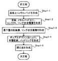
このような半導体装置は、例えば、図2のフローチャートに示す製造工程により形成される。 Such a semiconductor device is formed by, for example, a manufacturing process shown in the flowchart of FIG.
先ず、図3(a)に示すように、基板10の素子領域11にトランジスタ等の能動素子を形成し、続いて基板10上に、バリアメタル層181、Al層182を順次形成する。そして、レジスト膜を塗布形成した後、パターニングして、非素子領域17上の所定領域にマスクを形成し、露出部分をRIE(Reactive Ion Etching)などにより除去することにより、メタルパッド18を形成する(Step1−1)。 First, as shown in FIG. 3A, an active element such as a transistor is formed in the
次いで、図3(b)に示すように、基板10上に絶縁層12を形成した後、基板10及びメタルパッド18に到達するコンタクトホール(図示せず)と、環状の開口部(図示せず)を形成する。そして、コンタクトホール、環状の開口部をWなどで充填することにより、基板コンタクト151、パッドコンタクト152と、リング状の金属層200を形成する(Step1−2)。 Next, as shown in FIG. 3B, after the
そして、図3(c)に示すように、その上層に、low−k膜131aを形成した後、配線パターン及びリングパターンの溝(図示せず)を形成し、Cuめっきにより溝中に、最下層の配線層161a及びリング状の金属層201aを形成する(Step1−3)。なお、金属層201aは金属層200と接触している。 Then, as shown in FIG. 3C, after forming a low-
次いで、図3(d)に示すように、基板10上にcap膜132a、low−k膜131bを順次形成し、デュアルダマシン法により、配線パターン、ビアパターン及びリングパターンの溝を形成した後、ビア162a、配線層161b及びリング状の金属層202a、201bを形成する。ここで、金属層202aは金属層201b及び金属層201aに接触している。同様に、図3(e)に示すように、同様に順次cap膜132b、low−k膜131cを形成し、ビア162b、配線層161c及びリング状の金属層202b、201cを形成する。ここでも、金属層202bは金属層201c及び金属層201bに接触している。このようにして、多層配線16を形成するとともに、パッドリング20を形成する(Step1−4)。 Next, as shown in FIG. 3D, a
さらに、図3(f)に示すように、配線層161c、low−k膜131a及び金属層201c上にcap膜132c、パシベーション膜14を形成した後、レジスト(図示せず)を塗布、パターニングする。そして、パターニングしたレジストをマスクとしてパシベーション膜14及び層間絶縁膜13をRIEなどにより除去することにより、開口窓19を形成し、メタルパッド18表面のAl層182を露出させる(Step1−5)。 Further, as shown in FIG. 3F, after forming the
そして、ワイヤ21により、メタルパッド18が、開口窓19を通して、ボンディングされ、図1に示すような半導体装置が形成される。 Then, the
本実施形態の半導体装置によれば、最下層の配線層161よりも基板10側にメタルパッド18を形成する構造とすることにより、素子領域11上でワイヤーボンディングを行わないため、ワイヤーボンディング時の荷重によるlow−k膜131の変形やクラッキングの発生を回避することができる。そのため、low−k膜131の吸湿によるバリアメタル膜の酸化を抑え、半導体装置の信頼性の低下を抑制することが可能となる。 According to the semiconductor device of this embodiment, since the
また、本実施形態において、最下層の配線層よりも基板10側に位置するメタルパッドに到達する開口窓を設けているため、開口窓壁面に層間絶縁膜が露出し、壁面から水分が侵入する可能性がある。しかしながら、開口窓を取り囲むように、パッドリングを形成することにより、開口窓からの水分の侵入を抑えることができる。従って、low−k膜の吸湿によるバリアメタル膜の酸化を抑え、半導体装置の信頼性の低下を抑制することが可能となる。 In the present embodiment, since the opening window reaching the metal pad located on the
また、従来は、メタルパッド形成の際、例えばi線を用いたリソグラフィを2回行う必要があったが、本実施形態によれば、メタルパッド形成のためのリソグラフィを1回に削減することができる。 Conventionally, when forming a metal pad, it has been necessary to perform lithography using, for example, i-line twice, but according to the present embodiment, the lithography for forming the metal pad can be reduced to one time. it can.
さらに、本実施形態によれば、メタルパッドの表面層をこれまでと同様のAl層とすることができ、これまでの技術との互換性を保つことが可能となる。但し、表面層はAl層に限定されるものではなく、導電性を有する層であればよい。 Furthermore, according to the present embodiment, the surface layer of the metal pad can be the same Al layer as before, and compatibility with conventional techniques can be maintained. However, the surface layer is not limited to the Al layer, and may be any layer having conductivity.
(第2の実施形態)
本実施形態の半導体装置において、層間絶縁膜に開口窓を設ける構造は第1の実施形態と同様であるが、メタルパッドの構造が異なっている。(Second Embodiment)
In the semiconductor device of this embodiment, the structure in which the opening window is provided in the interlayer insulating film is the same as that of the first embodiment, but the structure of the metal pad is different.
図4に、本実施形態の半導体装置の断面図を示す。図に示すように、第1の実施形態と同様に、基板40の素子領域41上に、絶縁層42が形成されている。絶縁層42上には、第1の実施形態と同様に、例えばそれぞれ3層交互に形成された、low−k膜431a、431b、431cと、cap膜432a、432b、432cから構成される層間絶縁膜43が形成されている。層間絶縁膜43上には、パシベーション膜44が形成されている。 FIG. 4 shows a cross-sectional view of the semiconductor device of this embodiment. As shown in the figure, an insulating
なお、本実施形態において、層間絶縁膜をそれぞれ3層としているが、第1の実施形態と同様に、積層数はこれに限定されるものではなく、例えば10層以上で適宜設けることができる。後述する配線層、ビアについても、同様である。 In the present embodiment, each of the interlayer insulating films has three layers, but the number of stacked layers is not limited to this, as in the first embodiment, and for example, ten or more layers can be provided as appropriate. The same applies to wiring layers and vias described later.
素子領域41上の絶縁層42には、基板コンタクト45が形成され、その上層には、それぞれlow−k膜431、cap膜432を介して、それぞれ交互に形成され、所定パターンの配線層461a、461b、461c、ビア462a、462bを有する多層配線46が形成されている。 A
素子領域41以外の領域である非素子領域47上には、最下層の配線層461aよりも半導体基板40側に、W層481、Al層482などから構成されるメタルパッド48が形成されている。メタルパッド48は、配線層461a、461b、461c、ビア462a、462bを介して、素子領域41上の多層配線46と接続されている。さらに、メタルパッド48に到達する開口窓49が、パシベーション膜44及び層間絶縁膜43を貫通するように設けられている。 On the
そして、メタルパッド48上の層間絶縁膜43を貫通し、開口窓49を取り囲むように、パッドリング50が設けられている。パッドリング50は、配線層461a、461b、461c、ビア462a、462bとそれぞれ同層に同じ材料で形成されるリング状の金属層501a、501b、501c、502a、502bの積層体から構成されている。 A
そして、リードフレーム(図示せず)などと接続されたワイヤ51が、開口窓49を通り、メタルパッド48にボンディングされている。 A wire 51 connected to a lead frame (not shown) or the like passes through the opening
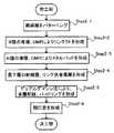
このような半導体装置は、例えば、図5のフローチャートに示す製造工程により形成される。 Such a semiconductor device is formed by, for example, a manufacturing process shown in the flowchart of FIG.
先ず、図6(a)に示すように、基板40の素子領域41にトランジスタ等の能動素子を形成し、続いて基板40上に、絶縁層42を形成する。そして、レジストを塗布、パターニングし、RIEなどにより、基板40の素子領域41上に基板40に到達するコンタクトホール61を形成するとともに、非素子領域47上に開口部62を形成する(Step2−1)。 First, as shown in FIG. 6A, active elements such as transistors are formed in the
次いで、図6(b)に示すように、W膜を堆積し、CMP(Chemical Mechanical Polishing)法により平坦化することにより、コンタクトホール61をWで埋め込み、基板コンタクト45を形成するとともに、開口部62内にW層481を形成する(Step2−2)。 Next, as shown in FIG. 6B, a W film is deposited and planarized by a CMP (Chemical Mechanical Polishing) method, so that the
さらに、図6(c)に示すように、Al膜を堆積し、CMP法により平坦化することにより、W層481の形成された開口部62内にAl層482を形成し、開口部62内にW層481、Al層482を有するメタルパッド48を形成する(Step2−3)。 Further, as shown in FIG. 6C, an Al film is deposited and flattened by a CMP method to form an
なお、このとき、W膜を形成してコンタクトホール61を埋め込み、連続してAl膜を形成した後、CMP法により一括で平坦化してメタルパッド48を形成してもよい。 At this time, a metal film 48 may be formed by forming a W film, filling the
そして、第1の実施形態と同様に、図6(d)に示すように、その上層に、low−k膜431aを形成した後、配線パターン及びリングパターンの溝(図示せず)を形成し、Cuめっきにより溝中に、最下層の配線層461a及びリング状の金属層501aを形成する(Step2−4)。 Then, as in the first embodiment, as shown in FIG. 6D, a low-
次いで、図6(e)に示すように、cap膜431b、low−k膜432aを順次形成し、デュアルダマシン法により、配線パターン、ビアパターン及びリングパターンの溝を形成した後、ビア462a、配線層461b及びリング状の金属層502a、501bを形成する。同様に、図6(f)に示すように、同様に順次cap膜432b、low−k膜431cを形成し、ビア462b、配線層461c及びリング状の金属層501cを形成する。このようにして、多層配線46を形成するとともに、パッドリング50を形成する(Step2−5)。 Next, as shown in FIG. 6E, a
さらに、図6(g)に示すように、cap膜431c、パシベーション膜44を形成した後、レジスト(図示せず)を塗布、パターニングする。そして、露出部分のパシベーション膜44及び層間絶縁膜43をRIEなどにより除去することにより、開口窓49を形成し、メタルパッド48表面のAl層482を露出させる(Step2−6)。 Further, as shown in FIG. 6G, after forming a
そして、ワイヤ51により、メタルパッド48が、開口窓49を通して、ボンディングされ、図4に示すような半導体装置が形成される。 Then, the metal pad 48 is bonded by the wire 51 through the opening
本実施形態の半導体装置によれば、第1の実施形態と同様に、最下層の配線層よりも半導体基板側にメタルパッドを形成する構造とすることにより、素子領域上でワイヤーボンディングを行わないため、ワイヤーボンディング時の荷重によるlow−k膜の変形やクラッキングの発生を回避することができる。そのため、low−k膜の吸湿によるバリアメタル膜の酸化を抑え、半導体装置の信頼性の低下を抑制することが可能となる。 According to the semiconductor device of the present embodiment, as in the first embodiment, wire bonding is not performed on the element region by forming a metal pad on the semiconductor substrate side of the lowermost wiring layer. Therefore, the deformation of the low-k film and the occurrence of cracking due to the load during wire bonding can be avoided. Therefore, it becomes possible to suppress the oxidation of the barrier metal film due to the moisture absorption of the low-k film, and to suppress the deterioration of the reliability of the semiconductor device.
また、第1の実施形態と同様に、最下層の配線層よりも半導体基板側のメタルパッドに到達する開口窓を設ける構造とすることにより、開口窓壁面に層間絶縁膜が露出し、壁面からの水分の侵入が問題となる。そこで、本実施形態のように、開口窓を取り囲むように、パッドリングを形成することにより、開口窓からの水分の侵入を抑えることができる。従って、low−k膜の吸湿によるバリアメタル膜の酸化を抑え、半導体装置の信頼性の低下を抑制することが可能となる。 Further, similarly to the first embodiment, by providing an opening window that reaches the metal pad on the semiconductor substrate side rather than the lowermost wiring layer, the interlayer insulating film is exposed on the wall surface of the opening window. Intrusion of moisture becomes a problem. Therefore, as in the present embodiment, the intrusion of moisture from the opening window can be suppressed by forming the pad ring so as to surround the opening window. Therefore, it is possible to suppress oxidation of the barrier metal film due to moisture absorption of the low-k film, and to suppress a decrease in reliability of the semiconductor device.
また、本実施形態によれば、メタルパッドを絶縁層内にコンタクト形成と同時に埋め込み形成することができるため、新たなリソグラフィ工程を設けることなく、メタルパッドを形成することができる。従って、従来は、メタルパッド形成の際、例えばi線を用いたリソグラフィを2回行う必要があったが、この工程を削減することが可能となる。 Further, according to the present embodiment, the metal pad can be embedded in the insulating layer at the same time as the contact formation, so that the metal pad can be formed without providing a new lithography process. Therefore, conventionally, when forming a metal pad, for example, lithography using i-line had to be performed twice, but this process can be reduced.
さらに、本実施形態によれば、第1の実施形態と同様に、メタルパッドの表面層をこれまでと同様のAl層とすることができ、これまでの技術との互換性を保つことが可能となる。但し、表面層はAl層に限定されるものではなく、導電性を有する層であればよい。 Furthermore, according to the present embodiment, as in the first embodiment, the surface layer of the metal pad can be made the same Al layer as before, and compatibility with conventional techniques can be maintained. It becomes. However, the surface layer is not limited to the Al layer, and may be any layer having conductivity.
これら実施形態において、半導体基板上に設けられる絶縁層として、通常用いられるTEOS膜などを用いることができるが、より高速化、低消費電力化を図るために、low−k膜を用いることも可能である。また、low−k膜としては、SiOC膜のみならず、CVD(Chemical Vapor Deposition)法や、塗布法などにより形成されたMSQ(Methylsilsesquioxane)や、ポリイミド系などの有機ポリマー系などから構成される膜を用いることができる。 In these embodiments, a commonly used TEOS film or the like can be used as the insulating layer provided on the semiconductor substrate, but a low-k film can also be used in order to achieve higher speed and lower power consumption. It is. The low-k film is not only a SiOC film but also a film made of MSQ (Methylsilsesquioxane) formed by a CVD (Chemical Vapor Deposition) method or a coating method, an organic polymer type such as a polyimide type, etc. Can be used.
尚、本発明は、上述した実施形態に限定されるものではない。その他要旨を逸脱しない範囲で種々変形して実施することができる。 In addition, this invention is not limited to embodiment mentioned above. Various other modifications can be made without departing from the scope of the invention.
10、40…基板、11、41…素子領域、12、42…絶縁層、13、43…層間絶縁膜、131a、131b、131c、431a、431b、431c…low−k膜、132a、132b、132c、432a、432b、432c…cap膜、14、44…パシベーション膜、151、45…基板コンタクト、152…パッドコンタクト、16、46…多層配線、161a、161b、161c、461a、461b、461c…配線層、162a、162b、462a、462b…ビア、18、48…メタルパッド、181…バリアメタル層、182、482…Al層、19、49…開口窓、20、50…パッドリング、200、201a、201b、201c、202a、202b、501a、501b、501c、502a、502b…リング状の金属層、21、51…ワイヤ、481…W層、61…コンタクトホール、62…開口部 DESCRIPTION OF
Claims (5)
Translated fromJapanese前記絶縁層上に形成された複数の低誘電率膜を含む層間絶縁膜と、
前記層間絶縁膜中にそれぞれ形成される複数の配線層及びビアからなる多層配線と、
前記複数の配線層のうち最下層の配線層より前記基板側に形成されたメタルパッドと、
前記メタルパッドの一部の領域上の前記絶縁層及び層間絶縁膜が除去されて形成された開口部と、
前記メタルパッド上に、前記複数の層間絶縁膜を貫通し、前記開口部を取り囲むように設けられるパッドリングと、
を備えることを特徴とする半導体装置。An insulating layer formed on the substrate;
An interlayer insulating filmincluding a plurality oflow dielectric constant films formed on the insulating layer;
A multilayer wiring composed of a plurality of wiring layers and vias respectively formed in the interlayer insulating film;
Metal pads formed on the substrate side from the lowermost wiring layer among the plurality of wiring layers,
An opening formed by removing the insulating layer and the interlayer insulating film on a partial region of the metal pad;
A pad ring provided on the metal pad so as to penetrate the plurality of interlayer insulating films and surround the opening;
A semiconductor device comprising:
前記基板上に絶縁層を形成し、
前記素子領域上の前記絶縁層に、前記基板に到達するコンタクトホールを形成するとともに、前記素子領域以外の領域上の前記絶縁層に開口部を形成し、
前記コンタクトホール内にコンタクトを埋め込み形成し、
前記開口部内にメタルパッドを埋め込み形成し、
前記絶縁層上に複数の低誘電率膜を含む層間絶縁膜と、複数の配線層及びビアを有する多層配線を形成するとともに、前記メタルパッド上に前記複数の層間絶縁膜を貫通するようにパッドリングを形成し、
前記パッドリングに取り囲まれた領域の前記層間絶縁膜を除去し、前記メタルパッドを露出させる、
ことを特徴とする半導体装置の製造方法。An element region is formed on the substrate,
Forming an insulating layer on the substrate;
A contact hole reaching the substrate is formed in the insulating layer on the element region, and an opening is formed in the insulating layer on a region other than the element region,
Forming a contact in the contact hole;
A metal pad is embedded in the opening,
An interlayer insulating filmincluding a plurality oflow dielectric constant films and a multilayer wiring having a plurality of wiring layers and vias are formed on the insulating layer, and a pad is formed so as to penetrate the plurality of interlayer insulating films on the metal pad Forming a ring,
Removing the interlayer insulating film in a region surrounded by the pad ring and exposing the metal pad;
A method for manufacturing a semiconductor device.
Priority Applications (2)
| Application Number | Priority Date | Filing Date | Title |
|---|---|---|---|
| JP2010132160AJP5582879B2 (en) | 2010-06-09 | 2010-06-09 | Semiconductor device and manufacturing method thereof |
| US13/048,176US8536710B2 (en) | 2010-06-09 | 2011-03-15 | Semiconductor device and manufacturing method thereof |
Applications Claiming Priority (1)
| Application Number | Priority Date | Filing Date | Title |
|---|---|---|---|
| JP2010132160AJP5582879B2 (en) | 2010-06-09 | 2010-06-09 | Semiconductor device and manufacturing method thereof |
Publications (2)
| Publication Number | Publication Date |
|---|---|
| JP2011258762A JP2011258762A (en) | 2011-12-22 |
| JP5582879B2true JP5582879B2 (en) | 2014-09-03 |
Family
ID=45095570
Family Applications (1)
| Application Number | Title | Priority Date | Filing Date |
|---|---|---|---|
| JP2010132160AExpired - Fee RelatedJP5582879B2 (en) | 2010-06-09 | 2010-06-09 | Semiconductor device and manufacturing method thereof |
Country Status (2)
| Country | Link |
|---|---|
| US (1) | US8536710B2 (en) |
| JP (1) | JP5582879B2 (en) |
Families Citing this family (2)
| Publication number | Priority date | Publication date | Assignee | Title |
|---|---|---|---|---|
| US9570430B2 (en)* | 2014-05-13 | 2017-02-14 | GlobalFoundries, Inc. | Articles including bonded metal structures and methods of preparing the same |
| US11876072B2 (en)* | 2021-09-02 | 2024-01-16 | Nanya Technology Corporation | Method for preparing semiconductor device with wire bond |
Family Cites Families (20)
| Publication number | Priority date | Publication date | Assignee | Title |
|---|---|---|---|---|
| EP0090066B1 (en)* | 1982-03-31 | 1990-05-30 | Ibm Deutschland Gmbh | Solid-state television camera |
| US5543586A (en)* | 1994-03-11 | 1996-08-06 | The Panda Project | Apparatus having inner layers supporting surface-mount components |
| JP3906522B2 (en)* | 1997-06-10 | 2007-04-18 | ソニー株式会社 | Manufacturing method of semiconductor device |
| JP3121311B2 (en)* | 1998-05-26 | 2000-12-25 | 日本電気株式会社 | Multilayer wiring structure, semiconductor device having the same, and manufacturing method thereof |
| JP2000012604A (en)* | 1998-06-22 | 2000-01-14 | Toshiba Corp | Semiconductor device and method of manufacturing the same |
| JP2974022B1 (en)* | 1998-10-01 | 1999-11-08 | ヤマハ株式会社 | Bonding pad structure of semiconductor device |
| JP2001267323A (en) | 2000-03-21 | 2001-09-28 | Matsushita Electric Ind Co Ltd | Semiconductor device and manufacturing method thereof |
| US6362531B1 (en)* | 2000-05-04 | 2002-03-26 | International Business Machines Corporation | Recessed bond pad |
| TW484196B (en)* | 2001-06-05 | 2002-04-21 | United Microelectronics Corp | Bonding pad structure |
| JP4801296B2 (en)* | 2001-09-07 | 2011-10-26 | 富士通セミコンダクター株式会社 | Semiconductor device and manufacturing method thereof |
| JP3811473B2 (en)* | 2003-02-25 | 2006-08-23 | 富士通株式会社 | Semiconductor device |
| US6864578B2 (en)* | 2003-04-03 | 2005-03-08 | International Business Machines Corporation | Internally reinforced bond pads |
| US7067902B2 (en)* | 2003-12-02 | 2006-06-27 | International Business Machines Corporation | Building metal pillars in a chip for structure support |
| US7071575B2 (en)* | 2004-11-10 | 2006-07-04 | United Microelectronics Corp. | Semiconductor chip capable of implementing wire bonding over active circuits |
| JP2006190839A (en)* | 2005-01-06 | 2006-07-20 | Matsushita Electric Ind Co Ltd | Semiconductor device and manufacturing method thereof |
| JP5141550B2 (en)* | 2006-03-08 | 2013-02-13 | 富士通セミコンダクター株式会社 | Semiconductor device and manufacturing method thereof |
| JP5111878B2 (en)* | 2007-01-31 | 2013-01-09 | ルネサスエレクトロニクス株式会社 | Manufacturing method of semiconductor device |
| US20080246152A1 (en)* | 2007-04-04 | 2008-10-09 | Taiwan Semiconductor Manufacturing Co., Ltd. | Semiconductor device with bonding pad |
| JP4609497B2 (en)* | 2008-01-21 | 2011-01-12 | ソニー株式会社 | Solid-state imaging device, manufacturing method thereof, and camera |
| JP2010093161A (en)* | 2008-10-10 | 2010-04-22 | Panasonic Corp | Semiconductor device |
- 2010
- 2010-06-09JPJP2010132160Apatent/JP5582879B2/ennot_activeExpired - Fee Related
- 2011
- 2011-03-15USUS13/048,176patent/US8536710B2/enactiveActive
Also Published As
| Publication number | Publication date |
|---|---|
| JP2011258762A (en) | 2011-12-22 |
| US20110304030A1 (en) | 2011-12-15 |
| US8536710B2 (en) | 2013-09-17 |
Similar Documents
| Publication | Publication Date | Title |
|---|---|---|
| US20220359274A1 (en) | Method and Apparatus for Back End of Line Semiconductor Device Processing | |
| CN106935544B (en) | Semiconductor device and method for forming the same | |
| KR100902581B1 (en) | Stack Capacitors in Semiconductor Devices and Methods of Forming Them | |
| JP4280204B2 (en) | Semiconductor device | |
| US20100244199A1 (en) | Semiconductor device and method for manufacturing semiconductor device | |
| JP2009147218A (en) | Semiconductor device and manufacturing method thereof | |
| JP2011139103A (en) | Semiconductor device | |
| JP2004080044A (en) | Method of forming metal wiring for semiconductor device using buffer layer on trench sidewall and device manufactured thereby | |
| JP2010287831A (en) | Semiconductor device and manufacturing method thereof | |
| JP2012038961A (en) | Semiconductor device and method of manufacturing the same | |
| JP4675393B2 (en) | Semiconductor device and manufacturing method of semiconductor device | |
| KR20130092825A (en) | Semicoductor devices having through vias and methods for fabricating the same | |
| US9287214B2 (en) | Semiconductor device | |
| JP2009295733A (en) | Semiconductor apparatus and method of manufacturing the same | |
| TWI660468B (en) | Package structure and manufacturing method thereof | |
| JP3777182B2 (en) | Method for reducing thermomechanical stress in an interconnect structure and method for forming an interconnect structure | |
| JP5582879B2 (en) | Semiconductor device and manufacturing method thereof | |
| CN110112064A (en) | A kind of semiconductor devices and preparation method thereof | |
| JP4436989B2 (en) | Manufacturing method of semiconductor device | |
| JP2012160547A (en) | Semiconductor device and manufacturing method of the same | |
| JP2003218114A (en) | Semiconductor device and manufacturing method thereof | |
| JP4814694B2 (en) | Semiconductor device | |
| JP5041088B2 (en) | Semiconductor device | |
| JP2014175525A (en) | Semiconductor device and manufacturing method of the same | |
| KR20090055772A (en) | Metal wiring formation method of semiconductor device |
Legal Events
| Date | Code | Title | Description |
|---|---|---|---|
| A621 | Written request for application examination | Free format text:JAPANESE INTERMEDIATE CODE: A621 Effective date:20120810 | |
| A977 | Report on retrieval | Free format text:JAPANESE INTERMEDIATE CODE: A971007 Effective date:20131016 | |
| A131 | Notification of reasons for refusal | Free format text:JAPANESE INTERMEDIATE CODE: A131 Effective date:20131112 | |
| A521 | Request for written amendment filed | Free format text:JAPANESE INTERMEDIATE CODE: A523 Effective date:20140110 | |
| TRDD | Decision of grant or rejection written | ||
| A01 | Written decision to grant a patent or to grant a registration (utility model) | Free format text:JAPANESE INTERMEDIATE CODE: A01 Effective date:20140617 | |
| A61 | First payment of annual fees (during grant procedure) | Free format text:JAPANESE INTERMEDIATE CODE: A61 Effective date:20140715 | |
| R151 | Written notification of patent or utility model registration | Ref document number:5582879 Country of ref document:JP Free format text:JAPANESE INTERMEDIATE CODE: R151 | |
| R250 | Receipt of annual fees | Free format text:JAPANESE INTERMEDIATE CODE: R250 | |
| LAPS | Cancellation because of no payment of annual fees |