JP5581677B2 - Electrophoretic display device and electronic apparatus - Google Patents
Electrophoretic display device and electronic apparatusDownload PDFInfo
- Publication number
- JP5581677B2 JP5581677B2JP2009276411AJP2009276411AJP5581677B2JP 5581677 B2JP5581677 B2JP 5581677B2JP 2009276411 AJP2009276411 AJP 2009276411AJP 2009276411 AJP2009276411 AJP 2009276411AJP 5581677 B2JP5581677 B2JP 5581677B2
- Authority
- JP
- Japan
- Prior art keywords
- electrode
- pixel
- display device
- electrophoretic
- display
- Prior art date
- Legal status (The legal status is an assumption and is not a legal conclusion. Google has not performed a legal analysis and makes no representation as to the accuracy of the status listed.)
- Active
Links
Images


Classifications
- G—PHYSICS
- G09—EDUCATION; CRYPTOGRAPHY; DISPLAY; ADVERTISING; SEALS
- G09G—ARRANGEMENTS OR CIRCUITS FOR CONTROL OF INDICATING DEVICES USING STATIC MEANS TO PRESENT VARIABLE INFORMATION
- G09G3/00—Control arrangements or circuits, of interest only in connection with visual indicators other than cathode-ray tubes
- G09G3/20—Control arrangements or circuits, of interest only in connection with visual indicators other than cathode-ray tubes for presentation of an assembly of a number of characters, e.g. a page, by composing the assembly by combination of individual elements arranged in a matrix no fixed position being assigned to or needed to be assigned to the individual characters or partial characters
- G09G3/34—Control arrangements or circuits, of interest only in connection with visual indicators other than cathode-ray tubes for presentation of an assembly of a number of characters, e.g. a page, by composing the assembly by combination of individual elements arranged in a matrix no fixed position being assigned to or needed to be assigned to the individual characters or partial characters by control of light from an independent source
- G09G3/3433—Control arrangements or circuits, of interest only in connection with visual indicators other than cathode-ray tubes for presentation of an assembly of a number of characters, e.g. a page, by composing the assembly by combination of individual elements arranged in a matrix no fixed position being assigned to or needed to be assigned to the individual characters or partial characters by control of light from an independent source using light modulating elements actuated by an electric field and being other than liquid crystal devices and electrochromic devices
- G09G3/344—Control arrangements or circuits, of interest only in connection with visual indicators other than cathode-ray tubes for presentation of an assembly of a number of characters, e.g. a page, by composing the assembly by combination of individual elements arranged in a matrix no fixed position being assigned to or needed to be assigned to the individual characters or partial characters by control of light from an independent source using light modulating elements actuated by an electric field and being other than liquid crystal devices and electrochromic devices based on particles moving in a fluid or in a gas, e.g. electrophoretic devices
- G09G3/3446—Control arrangements or circuits, of interest only in connection with visual indicators other than cathode-ray tubes for presentation of an assembly of a number of characters, e.g. a page, by composing the assembly by combination of individual elements arranged in a matrix no fixed position being assigned to or needed to be assigned to the individual characters or partial characters by control of light from an independent source using light modulating elements actuated by an electric field and being other than liquid crystal devices and electrochromic devices based on particles moving in a fluid or in a gas, e.g. electrophoretic devices with more than two electrodes controlling the modulating element
- G—PHYSICS
- G02—OPTICS
- G02F—OPTICAL DEVICES OR ARRANGEMENTS FOR THE CONTROL OF LIGHT BY MODIFICATION OF THE OPTICAL PROPERTIES OF THE MEDIA OF THE ELEMENTS INVOLVED THEREIN; NON-LINEAR OPTICS; FREQUENCY-CHANGING OF LIGHT; OPTICAL LOGIC ELEMENTS; OPTICAL ANALOGUE/DIGITAL CONVERTERS
- G02F1/00—Devices or arrangements for the control of the intensity, colour, phase, polarisation or direction of light arriving from an independent light source, e.g. switching, gating or modulating; Non-linear optics
- G02F1/01—Devices or arrangements for the control of the intensity, colour, phase, polarisation or direction of light arriving from an independent light source, e.g. switching, gating or modulating; Non-linear optics for the control of the intensity, phase, polarisation or colour
- G02F1/165—Devices or arrangements for the control of the intensity, colour, phase, polarisation or direction of light arriving from an independent light source, e.g. switching, gating or modulating; Non-linear optics for the control of the intensity, phase, polarisation or colour based on translational movement of particles in a fluid under the influence of an applied field
- G02F1/166—Devices or arrangements for the control of the intensity, colour, phase, polarisation or direction of light arriving from an independent light source, e.g. switching, gating or modulating; Non-linear optics for the control of the intensity, phase, polarisation or colour based on translational movement of particles in a fluid under the influence of an applied field characterised by the electro-optical or magneto-optical effect
- G02F1/167—Devices or arrangements for the control of the intensity, colour, phase, polarisation or direction of light arriving from an independent light source, e.g. switching, gating or modulating; Non-linear optics for the control of the intensity, phase, polarisation or colour based on translational movement of particles in a fluid under the influence of an applied field characterised by the electro-optical or magneto-optical effect by electrophoresis
- G—PHYSICS
- G02—OPTICS
- G02F—OPTICAL DEVICES OR ARRANGEMENTS FOR THE CONTROL OF LIGHT BY MODIFICATION OF THE OPTICAL PROPERTIES OF THE MEDIA OF THE ELEMENTS INVOLVED THEREIN; NON-LINEAR OPTICS; FREQUENCY-CHANGING OF LIGHT; OPTICAL LOGIC ELEMENTS; OPTICAL ANALOGUE/DIGITAL CONVERTERS
- G02F1/00—Devices or arrangements for the control of the intensity, colour, phase, polarisation or direction of light arriving from an independent light source, e.g. switching, gating or modulating; Non-linear optics
- G02F1/01—Devices or arrangements for the control of the intensity, colour, phase, polarisation or direction of light arriving from an independent light source, e.g. switching, gating or modulating; Non-linear optics for the control of the intensity, phase, polarisation or colour
- G02F1/165—Devices or arrangements for the control of the intensity, colour, phase, polarisation or direction of light arriving from an independent light source, e.g. switching, gating or modulating; Non-linear optics for the control of the intensity, phase, polarisation or colour based on translational movement of particles in a fluid under the influence of an applied field
- G02F1/1675—Constructional details
- G02F1/1676—Electrodes
- G02F1/16761—Side-by-side arrangement of working electrodes and counter-electrodes
- G—PHYSICS
- G02—OPTICS
- G02F—OPTICAL DEVICES OR ARRANGEMENTS FOR THE CONTROL OF LIGHT BY MODIFICATION OF THE OPTICAL PROPERTIES OF THE MEDIA OF THE ELEMENTS INVOLVED THEREIN; NON-LINEAR OPTICS; FREQUENCY-CHANGING OF LIGHT; OPTICAL LOGIC ELEMENTS; OPTICAL ANALOGUE/DIGITAL CONVERTERS
- G02F1/00—Devices or arrangements for the control of the intensity, colour, phase, polarisation or direction of light arriving from an independent light source, e.g. switching, gating or modulating; Non-linear optics
- G02F1/01—Devices or arrangements for the control of the intensity, colour, phase, polarisation or direction of light arriving from an independent light source, e.g. switching, gating or modulating; Non-linear optics for the control of the intensity, phase, polarisation or colour
- G02F1/165—Devices or arrangements for the control of the intensity, colour, phase, polarisation or direction of light arriving from an independent light source, e.g. switching, gating or modulating; Non-linear optics for the control of the intensity, phase, polarisation or colour based on translational movement of particles in a fluid under the influence of an applied field
- G02F1/1675—Constructional details
- G02F1/1676—Electrodes
- G02F1/16762—Electrodes having three or more electrodes per pixel
- G—PHYSICS
- G02—OPTICS
- G02F—OPTICAL DEVICES OR ARRANGEMENTS FOR THE CONTROL OF LIGHT BY MODIFICATION OF THE OPTICAL PROPERTIES OF THE MEDIA OF THE ELEMENTS INVOLVED THEREIN; NON-LINEAR OPTICS; FREQUENCY-CHANGING OF LIGHT; OPTICAL LOGIC ELEMENTS; OPTICAL ANALOGUE/DIGITAL CONVERTERS
- G02F1/00—Devices or arrangements for the control of the intensity, colour, phase, polarisation or direction of light arriving from an independent light source, e.g. switching, gating or modulating; Non-linear optics
- G02F1/01—Devices or arrangements for the control of the intensity, colour, phase, polarisation or direction of light arriving from an independent light source, e.g. switching, gating or modulating; Non-linear optics for the control of the intensity, phase, polarisation or colour
- G02F1/165—Devices or arrangements for the control of the intensity, colour, phase, polarisation or direction of light arriving from an independent light source, e.g. switching, gating or modulating; Non-linear optics for the control of the intensity, phase, polarisation or colour based on translational movement of particles in a fluid under the influence of an applied field
- G02F1/1675—Constructional details
- G02F1/1676—Electrodes
- G02F1/16766—Electrodes for active matrices
- G—PHYSICS
- G02—OPTICS
- G02F—OPTICAL DEVICES OR ARRANGEMENTS FOR THE CONTROL OF LIGHT BY MODIFICATION OF THE OPTICAL PROPERTIES OF THE MEDIA OF THE ELEMENTS INVOLVED THEREIN; NON-LINEAR OPTICS; FREQUENCY-CHANGING OF LIGHT; OPTICAL LOGIC ELEMENTS; OPTICAL ANALOGUE/DIGITAL CONVERTERS
- G02F1/00—Devices or arrangements for the control of the intensity, colour, phase, polarisation or direction of light arriving from an independent light source, e.g. switching, gating or modulating; Non-linear optics
- G02F1/01—Devices or arrangements for the control of the intensity, colour, phase, polarisation or direction of light arriving from an independent light source, e.g. switching, gating or modulating; Non-linear optics for the control of the intensity, phase, polarisation or colour
- G02F1/165—Devices or arrangements for the control of the intensity, colour, phase, polarisation or direction of light arriving from an independent light source, e.g. switching, gating or modulating; Non-linear optics for the control of the intensity, phase, polarisation or colour based on translational movement of particles in a fluid under the influence of an applied field
- G02F1/1685—Operation of cells; Circuit arrangements affecting the entire cell
- G—PHYSICS
- G09—EDUCATION; CRYPTOGRAPHY; DISPLAY; ADVERTISING; SEALS
- G09G—ARRANGEMENTS OR CIRCUITS FOR CONTROL OF INDICATING DEVICES USING STATIC MEANS TO PRESENT VARIABLE INFORMATION
- G09G3/00—Control arrangements or circuits, of interest only in connection with visual indicators other than cathode-ray tubes
- G09G3/20—Control arrangements or circuits, of interest only in connection with visual indicators other than cathode-ray tubes for presentation of an assembly of a number of characters, e.g. a page, by composing the assembly by combination of individual elements arranged in a matrix no fixed position being assigned to or needed to be assigned to the individual characters or partial characters
- G09G3/2007—Display of intermediate tones
- G09G3/207—Display of intermediate tones by domain size control
- G—PHYSICS
- G02—OPTICS
- G02F—OPTICAL DEVICES OR ARRANGEMENTS FOR THE CONTROL OF LIGHT BY MODIFICATION OF THE OPTICAL PROPERTIES OF THE MEDIA OF THE ELEMENTS INVOLVED THEREIN; NON-LINEAR OPTICS; FREQUENCY-CHANGING OF LIGHT; OPTICAL LOGIC ELEMENTS; OPTICAL ANALOGUE/DIGITAL CONVERTERS
- G02F1/00—Devices or arrangements for the control of the intensity, colour, phase, polarisation or direction of light arriving from an independent light source, e.g. switching, gating or modulating; Non-linear optics
- G02F1/01—Devices or arrangements for the control of the intensity, colour, phase, polarisation or direction of light arriving from an independent light source, e.g. switching, gating or modulating; Non-linear optics for the control of the intensity, phase, polarisation or colour
- G02F1/165—Devices or arrangements for the control of the intensity, colour, phase, polarisation or direction of light arriving from an independent light source, e.g. switching, gating or modulating; Non-linear optics for the control of the intensity, phase, polarisation or colour based on translational movement of particles in a fluid under the influence of an applied field
- G02F1/1675—Constructional details
- G02F1/16757—Microcapsules
- G—PHYSICS
- G09—EDUCATION; CRYPTOGRAPHY; DISPLAY; ADVERTISING; SEALS
- G09G—ARRANGEMENTS OR CIRCUITS FOR CONTROL OF INDICATING DEVICES USING STATIC MEANS TO PRESENT VARIABLE INFORMATION
- G09G2310/00—Command of the display device
- G09G2310/02—Addressing, scanning or driving the display screen or processing steps related thereto
- G09G2310/0262—The addressing of the pixel, in a display other than an active matrix LCD, involving the control of two or more scan electrodes or two or more data electrodes, e.g. pixel voltage dependent on signals of two data electrodes
- G—PHYSICS
- G09—EDUCATION; CRYPTOGRAPHY; DISPLAY; ADVERTISING; SEALS
- G09G—ARRANGEMENTS OR CIRCUITS FOR CONTROL OF INDICATING DEVICES USING STATIC MEANS TO PRESENT VARIABLE INFORMATION
- G09G3/00—Control arrangements or circuits, of interest only in connection with visual indicators other than cathode-ray tubes
- G09G3/03—Control arrangements or circuits, of interest only in connection with visual indicators other than cathode-ray tubes specially adapted for displays having non-planar surfaces, e.g. curved displays
- G09G3/035—Control arrangements or circuits, of interest only in connection with visual indicators other than cathode-ray tubes specially adapted for displays having non-planar surfaces, e.g. curved displays for flexible display surfaces
Landscapes
- Physics & Mathematics (AREA)
- Nonlinear Science (AREA)
- General Physics & Mathematics (AREA)
- Optics & Photonics (AREA)
- Engineering & Computer Science (AREA)
- Computer Hardware Design (AREA)
- Theoretical Computer Science (AREA)
- Life Sciences & Earth Sciences (AREA)
- Chemical Kinetics & Catalysis (AREA)
- Electrochemistry (AREA)
- Molecular Biology (AREA)
- Chemical & Material Sciences (AREA)
- Health & Medical Sciences (AREA)
- Electrochromic Elements, Electrophoresis, Or Variable Reflection Or Absorption Elements (AREA)
- Control Of Indicators Other Than Cathode Ray Tubes (AREA)
Description
Translated fromJapanese 本発明は、電気泳動表示装置及び電子機器に関するものである。
The present invention relates to an electrophoretic display instrumentation置及 beauty electronics.
中間階調表示が可能な電気泳動表示装置として、1つの画素内に複数のサブピクセルを設け、サブピクセルごとに白表示と黒表示とを切り換えることで上記画素の階調を制御するものが知られている(例えば特許文献1参照)。 As an electrophoretic display device capable of intermediate gray scale display, a device in which a plurality of subpixels are provided in one pixel and the grayscale of the pixel is controlled by switching between white display and black display for each subpixel is known. (See, for example, Patent Document 1).
特許文献1記載の電気泳動表示装置によれば、画素を構成する個々のサブピクセルを中間階調表示させる必要がないため、中間階調における表示色の再現性に優れるという効果が得られる。しかしながら、階調数を増やすためにはサブピクセルの個数を増やさなければならないという課題があった。 According to the electrophoretic display device described in Patent Document 1, since it is not necessary to display the individual sub-pixels constituting the pixel in the intermediate gradation, an effect of excellent display color reproducibility in the intermediate gradation can be obtained. However, there is a problem that the number of subpixels must be increased in order to increase the number of gradations.
本発明は、上記従来技術の問題点に鑑み成されたものであって、サブピクセルの個数を増やすことなく多階調の表示を可能とした電気泳動表示装置及び電子機器を提供することを目的の一つとする。
The present invention, which was made in view of the problems of the prior art, to provide a multi-tone electrophoretic displayequipment and an electronic device which enables display of without increasing the number of subpixels One of the purposes.
本発明の電気泳動表示装置は、一対の基板間に電気泳動素子を挟持してなり、一方の前記基板に画素毎に形成された第1電極及び前記第1電極と同層に形成された第2電極と、他方の前記基板に形成され前記電気泳動素子を介して前記第1電極及び第2電極と対向する対向電極と、を有する電気泳動表示装置であって、前記第1電極が前記画素の中央部に配置された平面視略正方形状の島状部と前記島状部から延びる接続配線部とを有し、前記第2電極が前記島状部の外縁に沿って形成されたCリング形状に形成され、前記第1電極の前記接続配線部が、前記第2電極の前記Cリング形状の先端の開口部を経由して外側に引き出されており、前記第1電極と前記第2電極との電位差により階調を表示することを特徴とする。In the electrophoretic display device of the present invention, an electrophoretic element is sandwiched between a pair of substrates, and a first electrode formed for each pixel on one of the substrates and a first electrode formed in the same layer asthe first electrode . 2. An electrophoretic display device having two electrodes and a counter electrode formed on the other substrate and facing the first electrode and the second electrode through the electrophoretic element, wherein the first electrode is the pixel. A C-ring having a substantially square island-like portion in plan view and a connection wiring portion extending from the island-like portion, the second electrode being formed along an outer edge of the island-like portion The connection wiring portion of the first electrode is drawn out to the outside via the opening at the tip of the C-ring shape of the second electrode, and the first electrode and the second electrode A gray scale is displayed by the potential difference between the two.
この構成では、第1電極と第2電極との電位差に起因して形成される電界の歪みや横方向電界によって電気泳動素子内における電気泳動粒子の配置状態を自在に制御することができる。したがって本発明によれば、サブピクセルの個数を増やすことなく多階調表示を可能とした電気泳動表示装置を実現することができる。 In this configuration, the arrangement state of the electrophoretic particles in the electrophoretic element can be freely controlled by the distortion of the electric field formed due to the potential difference between the first electrode and the second electrode or the lateral electric field. Therefore, according to the present invention, it is possible to realize an electrophoretic display device that enables multi-gradation display without increasing the number of subpixels.
前記第1電極上における所定階調の表示領域の大きさを制御することで階調を表示することが好ましい。例えば、1つの画素内における黒表示領域の大きさを変化させることで、ユーザーに視認される画素の反射濃度を異ならせることができ、中間階調を滑らかに表示することができる。また、上記所定階調の表示領域自体は中間階調の領域ではなく、例えば黒表示や白表示となる。したがって、電気泳動素子の駆動を途中で停止させて中間階調表示を行う場合のように階調値によって応答時間が異なってしまうことはない。 It is preferable to display gradation by controlling the size of a display area of a predetermined gradation on the first electrode. For example, by changing the size of the black display area in one pixel, the reflection density of the pixel visually recognized by the user can be varied, and the intermediate gradation can be displayed smoothly. Further, the display area itself of the predetermined gradation is not an intermediate gradation area, and is, for example, black display or white display. Therefore, the response time does not differ depending on the gradation value as in the case of performing the intermediate gradation display by stopping the driving of the electrophoretic element.
前記画素領域内における第1の階調と第2の階調の割合を制御することで階調を表示することも好ましい。これにより、滑らかな多階調表示を得ることができる。 It is also preferable to display gradation by controlling the ratio between the first gradation and the second gradation in the pixel region. Thereby, a smooth multi-gradation display can be obtained.
前記第1電極と接続された第1スイッチング素子と前記第2電極と接続された第2スイッチング素子とを有し、前記第1スイッチング素子の入力端子と前記第2スイッチング素子の入力端子とが共通のデータ線に接続されていることも好ましい。
この構成によれば、第1電極及び第2電極に対して1本のデータ線を用いて画像信号を入力することができるため、データ線の数を少なくすることができ、駆動回路の規模を小さくすることができる。A first switching element connected to the first electrode; and a second switching element connected to the second electrode; and an input terminal of the first switching element and an input terminal of the second switching element are common. It is also preferable to be connected to the data line.
According to this configuration, since an image signal can be input using one data line for the first electrode and the second electrode, the number of data lines can be reduced, and the scale of the drive circuit can be reduced. Can be small.
複数の前記第1電極が相互に接続されている構成としてもよい。この構成によれば、複数の第1電極を一括して制御できるため、画素スイッチング素子の個数を減らすことができるとともに、駆動回路の規模も小さくすることができる。 A plurality of the first electrodes may be connected to each other. According to this configuration, since the plurality of first electrodes can be controlled collectively, the number of pixel switching elements can be reduced and the scale of the drive circuit can be reduced.
前記第1電極と接続された第3スイッチング素子と前記第2電極と接続された第2スイッチング素子とを有し、前記第3スイッチング素子の制御端子と前記第2スイッチング素子の制御端子とが共通の走査線に接続されていることも好ましい。
この構成によれば、1本の走査線を介した選択信号の入力により第2スイッチング素子と第3スイッチング素子のオンオフ動作を制御できるため、走査線の数を減らすことができ、駆動回路の規模を小さくすることができる。A third switching element connected to the first electrode and a second switching element connected to the second electrode, wherein a control terminal of the third switching element and a control terminal of the second switching element are common It is also preferable to be connected to the scanning line.
According to this configuration, since the on / off operation of the second switching element and the third switching element can be controlled by inputting a selection signal via one scanning line, the number of scanning lines can be reduced, and the scale of the driving circuit can be reduced. Can be reduced.
前記第1電極が前記画素の中央部に配置された島状部と前記島状部から延びる接続配線部とを有しており、前記第2電極が前記島状部の外縁に沿って形成されていることも好ましい。
この構成によれば、画素の中央部の第1電極上に形成される所定階調の表示領域の大きさを制御することで中間階調表示を行う電気泳動表示装置を提供することができる。The first electrode includes an island-like portion disposed at a central portion of the pixel and a connection wiring portion extending from the island-like portion, and the second electrode is formed along an outer edge of the island-like portion. It is also preferable.
According to this configuration, it is possible to provide an electrophoretic display device that performs intermediate gradation display by controlling the size of a display area of a predetermined gradation formed on the first electrode in the center of the pixel.
前記基板上に、前記第2電極と、前記第2電極を覆う絶縁膜と、前記絶縁膜上に部分的に形成された第1電極とがこの順に形成されていることも好ましい。
この構成によれば、第1電極と第2電極との間に電位差を生じさせた場合に、第1電極の端縁(エッジ部)とその近傍の第2電極との間に斜め方向の電界が形成され、かかる斜め電界により電気泳動素子の一部を対向電極側へ移動させないようにすることができる。これにより、多段階の中間階調表示が可能である。It is also preferable that the second electrode, the insulating film covering the second electrode, and the first electrode partially formed on the insulating film are formed in this order on the substrate.
According to this configuration, when a potential difference is generated between the first electrode and the second electrode, an oblique electric field is generated between the edge (edge portion) of the first electrode and the second electrode in the vicinity thereof. Thus, it is possible to prevent a part of the electrophoretic element from being moved to the counter electrode side by the oblique electric field. Thereby, multi-level halftone display is possible.
前記第1電極が櫛歯状の電極であることも好ましい。
この構成によれば、櫛歯状の電極に対応した平面領域に所定階調の表示領域を形成し、かかる表示領域の幅(太さ)を変化させることで階調値を異ならせる中間階調表示が可能である。It is also preferable that the first electrode is a comb-like electrode.
According to this configuration, an intermediate gradation in which a gradation area is formed by changing the width (thickness) of the display area by forming a display area of a predetermined gradation in a planar area corresponding to the comb-like electrode. Display is possible.
前記第1電極又は第2電極上に形成され前記第1電極又は前記第2電極から前記電気泳動素子側へ突出する突起部を有することも好ましい。
この構成によれば、立体構造物である突起部が電気泳動素子に突出されていることで、電気泳動素子内に横方向(基板面方向)の電界が形成されやすくなる。これにより、電気泳動粒子の一部が対向電極側へ移動しないように保持する作用をより確実に得られるようになり、中間階調表示の制御性を向上させることができる。It is also preferable to have a protrusion formed on the first electrode or the second electrode and protruding from the first electrode or the second electrode toward the electrophoretic element.
According to this configuration, since the protruding portion that is a three-dimensional structure protrudes from the electrophoretic element, an electric field in the lateral direction (substrate surface direction) is easily formed in the electrophoretic element. As a result, it is possible to more reliably obtain an action of holding a part of the electrophoretic particles so as not to move to the counter electrode side, and it is possible to improve the controllability of intermediate gradation display.
次に、本発明の電気泳動表示装置の駆動方法は、一対の基板間に電気泳動素子を挟持してなり、一方の前記基板に画素毎に形成された第1電極及び第2電極と、他方の前記基板に形成され前記電気泳動素子を介して前記第1電極及び第2電極と対向する対向電極と、を有する電気泳動表示装置の駆動方法であって、前記第1電極と前記対向電極とに前記画素に第1の階調を表示させる電位を入力するとともに、前記第2電極に所定の電位を入力し、前記画素に前記第1電極と前記第2電極との電位差に基づく階調を表示させることを特徴とする。 Next, according to the driving method of the electrophoretic display device of the present invention, the electrophoretic element is sandwiched between a pair of substrates, the first electrode and the second electrode formed for each pixel on one of the substrates, and the other A driving method for an electrophoretic display device, comprising: a counter electrode formed on the substrate and opposing the first electrode and the second electrode via the electrophoretic element, wherein the first electrode, the counter electrode, A potential for causing the pixel to display a first gradation is input, a predetermined potential is input to the second electrode, and a gradation based on a potential difference between the first electrode and the second electrode is input to the pixel. It is characterized by being displayed.
この駆動方法によれば、サブピクセル数を増やすことなく多段階の中階調表示を行うことができる。 According to this driving method, it is possible to perform multi-level medium gradation display without increasing the number of subpixels.
前記第1電極と前記第2電極との電位差によって前記第1電極上における前記第1の階調の表示領域の大きさを制御することが好ましい。
前記第1電極と前記第2電極との電位差によって前記画素内における前記第1の階調の表示領域の割合と前記第1の階調と異なる第2の階調の表示領域の割合を制御することも好ましい。
これらの駆動方法によれば、滑らかな中間階調表示が可能であるとともに、表示階調によって応答速度が異なってしまうのを回避でき、ユーザーが視認したときの違和感を低減することができる。It is preferable that the size of the display area of the first gradation on the first electrode is controlled by a potential difference between the first electrode and the second electrode.
The ratio of the display area of the first gradation in the pixel and the ratio of the display area of the second gradation different from the first gradation are controlled by the potential difference between the first electrode and the second electrode. It is also preferable.
According to these driving methods, smooth halftone display is possible, and it is possible to avoid that the response speed varies depending on the display gradation, and to reduce the uncomfortable feeling when the user visually recognizes.
本発明の電子機器は、先に記載の電気泳動表示装置を備えたことを特徴とする。
この構成によれば、サブピクセル数を増やすことなく多階調表示を可能とした表示手段を具備した電子機器を提供することができる。An electronic apparatus according to the present invention includes the electrophoretic display device described above.
According to this configuration, it is possible to provide an electronic apparatus including a display unit that can perform multi-gradation display without increasing the number of subpixels.
以下、図面を用いて本発明の実施の形態について説明する。
なお、本発明の範囲は、以下の実施の形態に限定されるものではなく、本発明の技術的思想の範囲内で任意に変更可能である。また、以下の図面においては、各構成をわかりやすくするために、実際の構造と各構造における縮尺や数等を異ならせる場合がある。Hereinafter, embodiments of the present invention will be described with reference to the drawings.
The scope of the present invention is not limited to the following embodiment, and can be arbitrarily changed within the scope of the technical idea of the present invention. Moreover, in the following drawings, in order to make each structure easy to understand, the actual structure may be different from the scale, number, or the like in each structure.
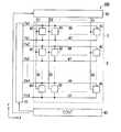
図1は、本発明の一実施の形態である電気泳動表示装置100の概略構成図である。
電気泳動表示装置100は、複数の画素40がマトリクス状に配列された表示部5を備えている。表示部5の周辺には、走査線駆動回路61、データ線駆動回路62、及びコントローラー(制御部)63が配置されている。走査線駆動回路61、及びデータ線駆動回路62は、それぞれコントローラー63と接続されている。コントローラー63は、上位装置から供給される画像データや同期信号に基づき、これらの駆動回路を総合的に制御する。FIG. 1 is a schematic configuration diagram of an
The
表示部5には走査線駆動回路61から延びる複数の第1走査線66及び複数の第2走査線67と、データ線駆動回路62から延びる複数のデータ線68とが形成されている。第1走査線66とデータ線68との交差位置に対応して画素40が設けられている。各々の画素40に対して、第1走査線66と第2走査線67とデータ線68とが接続されている。 In the
走査線駆動回路61は、m本の第1走査線66(Ya1、Ya2、…、Yam)と、m本の第2走査線67(Yb1、Yb2、…、Ybm)とを介して各々の画素40に接続されており、コントローラー63の制御のもと、1行目からm行目までの第1走査線66及び第2走査線67を順次選択し、画素40に設けられた第1トランジスタTR1(第1スイッチング素子;図2参照)及び第2トランジスタTR2(第2スイッチング素子;図2参照)のそれぞれのオンタイミングを規定する選択信号を供給する。より詳しくは、第1走査線66を介して第1トランジスタTR1に選択信号が供給され、第2走査線67を介して第2トランジスタTR2に選択信号が供給される。上記動作において、同一の画素40に接続された第1走査線66及び第2走査線67は同時に選択されることはなく、順に選択される。なお、第1走査線66を駆動する走査線駆動回路と、第2走査線67を駆動する走査線駆動回路とが別々の回路として設けられていてもよい。 The scanning
データ線駆動回路62は、n本のデータ線68(X1、X2、…、Xn)を介して各々の画素40に接続されており、コントローラー63の制御のもと、画素40の各々に対応する画素データを規定する画像信号を画素40に供給する。本実施形態の場合、データ線駆動回路62は、画素40の基準階調を規定する第1画像信号を第1トランジスタTR1に対して供給する一方、上記基準階調からの変位幅を規定する第2画像信号を第2トランジスタTR2に対して供給する。したがって、コントローラー63は、上位装置から入力された画像データ(画素データ)から1組の第1画像信号と第2画像信号を生成し、データ線駆動回路62に順次供給する。 The data line driving
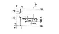
図2は、画素40の回路構成図である。
画素40には、第1トランジスタTR1と、第2トランジスタTR2と、第1電極35aと、第2電極35bと、電気泳動素子32と、共通電極37(対向電極)と、が設けられている。また、画素40には、第1走査線66と、第2走査線67と、データ線68とが接続されている。第1トランジスタTR1と第2トランジスタTR2はいずれもN−MOS(Negative Metal Oxide Semiconductor)トランジスタである。FIG. 2 is a circuit configuration diagram of the
The
画素40において、第1トランジスタTR1のゲートに第1走査線66が接続され、ソースにはデータ線68が接続され、ドレインには第1電極35aが接続されている。第2トランジスタTR2のゲートに第2走査線67が接続され、ソースに第1トランジスタTR1と共通のデータ線68が接続され、ドレインには第2電極35bが接続されている。 In the
なお、第1トランジスタTR1、及び第2トランジスタTR2は、それらと同等の機能を有する他の種類のスイッチング素子と置き換えてもよい。例えば、N−MOSトランジスタに代えてP−MOSトランジスタを用いてもよく、インバータやトランスミッションゲートを用いてもよい。
また、画素40に保持容量を設けてもよい。保持容量を設ける場合には、第1電極35aに接続され第1画像信号を保持する第1保持容量と、第2電極35bに接続され第2画像信号を保持する第2保持容量とを設けることが好ましい。ただし、上記の第1保持容量と第2保持容量のうちいずれか一方のみが設けられた構成とすることを妨げるものではない。The first transistor TR1 and the second transistor TR2 may be replaced with other types of switching elements having functions equivalent to those of the first transistor TR1 and the second transistor TR2. For example, a P-MOS transistor may be used instead of the N-MOS transistor, and an inverter or a transmission gate may be used.
Further, the
第1トランジスタTR1は、本実施形態の場合、画素40に対して基準階調を規定する第1画像信号の入力を制御するスイッチング素子であり、かかる第1画像信号の入力により画素40の階調を制御する領域の表示色(白又は黒)が決定される。
一方、第2トランジスタTR2は、画素40に対して基準階調からの変位幅を規定する第2画像信号の入力を制御するスイッチング素子であり、かかる第2画像信号の入力により画素40の平面領域に占める上記基準階調で表示された領域の大きさ又は形状が決定される。In the present embodiment, the first transistor TR1 is a switching element that controls the input of the first image signal that defines the reference gradation for the
On the other hand, the second transistor TR2 is a switching element that controls the input of the second image signal that defines the displacement width from the reference gradation with respect to the
次に、図3(a)は、表示部5における電気泳動表示装置100の部分断面図である。電気泳動表示装置100は、素子基板(第1基板)30と対向基板(第2基板)31との間に、複数のマイクロカプセル20を配列してなる電気泳動素子32を挟持した構成を備えている。 Next, FIG. 3A is a partial cross-sectional view of the
表示部5において、素子基板30の電気泳動素子32側には、図1や図2に示した第1走査線66、第2走査線67、データ線68、第1トランジスタTR1、第2トランジスタTR2などが形成された回路層34が設けられており、回路層34上に複数の画素電極35(第1電極35a、第2電極35b)が配列形成されている。なお、以下の説明では、1つの画素40に属する第1電極35aと第2電極35bとを合わせて画素電極35と称する場合がある。
素子基板30は、ガラスやプラスチック等からなる基板であり、画像表示面とは反対側に配置されるため透明なものでなくてもよい。画素電極35は、Cu(銅)箔上にニッケルメッキと金メッキとをこの順番で積層したものや、Al(アルミニウム)、ITO(インジウム・スズ酸化物)などにより形成された電気泳動素子32に電圧を印加する電極である。In the
The
一方、対向基板31の電気泳動素子32側には複数の画素電極35と対向する平面形状の共通電極37(対向電極)が形成されており、共通電極37上に電気泳動素子32が設けられている。
対向基板31はガラスやプラスチック等からなる基板であり、画像表示側に配置されるため透明基板とされる。共通電極37は、画素電極35とともに電気泳動素子32に電圧を印加する電極であり、MgAg(マグネシウム銀)、ITO(インジウム・スズ酸化物)、IZO(インジウム・亜鉛酸化物)などから形成された透明電極である。
そして、電気泳動素子32と画素電極35とが、接着剤層33を介して接着されることで、素子基板30と対向基板31とが接合されている。On the other hand, a planar common electrode 37 (opposite electrode) facing the plurality of
The
The
なお、電気泳動素子32は、あらかじめ対向基板31側に形成され、接着剤層33までを含めた電気泳動シートとして取り扱われるのが一般的である。製造工程において、電気泳動シートは接着剤層33の表面に保護用の離型シートが貼り付けられた状態で取り扱われる。そして、別途製造された素子基板30(画素電極35や各種回路などが形成されている)に対して、離型シートを剥がした当該電気泳動シートを貼り付けることによって、表示部5を形成する。このため、接着剤層33は画素電極35側のみに存在することになる。 In general, the
図3(b)は、マイクロカプセル20の模式断面図である。マイクロカプセル20は、例えば50μm程度の粒径を有しており、内部に分散媒21と、複数の白色粒子(電気泳動粒子)27と、複数の黒色粒子(電気泳動粒子)26とを封入した球状体である。マイクロカプセル20は、図3(a)に示すように共通電極37と画素電極35とに挟持され、1つの画素40内に1つ又は複数のマイクロカプセル20が配置される。 FIG. 3B is a schematic cross-sectional view of the
マイクロカプセル20の外殻部(壁膜)は、ポリメタクリル酸メチル、ポリメタクリル酸エチルなどのアクリル樹脂、ユリア樹脂、アラビアガムなどの透光性を持つ高分子樹脂などを用いて形成される。
分散媒21は、白色粒子27と黒色粒子26とをマイクロカプセル20内に分散させる液体である。分散媒21としては、水、アルコール系溶媒(メタノール、エタノール、イソプロパノール、ブタノール、オクタノール、メチルセルソルブなど)、エステル類(酢酸エチル、酢酸ブチルなど)、ケトン類(アセトン、メチルエチルケトン、メチルイソブチルケトンなど)、脂肪族炭化水素(ぺンタン、ヘキサン、オクタンなど)、脂環式炭化水素(シクロへキサン、メチルシクロへキサンなど)、芳香族炭化水素(ベンゼン、トルエン、長鎖アルキル基を有するベンゼン類(キシレン、ヘキシルベンゼン、ヘブチルベンゼン、オクチルベンゼン、ノニルベンゼン、デシルベンゼン、ウンデシルベンゼン、ドデシルベンゼン、トリデシルベンゼン、テトラデシルベンゼンなど))、ハロゲン化炭化水素(塩化メチレン、クロロホルム、四塩化炭素、1,2−ジクロロエタンなど)、カルボン酸塩などを例示することができ、その他の油類であってもよい。これらの物質は単独又は混合物として用いることができ、さらに界面活性剤などを配合してもよい。The outer shell portion (wall film) of the
The
白色粒子27は、例えば、二酸化チタン、亜鉛華、三酸化アンチモン等の白色顔料からなる粒子(高分子あるいはコロイド)であり、例えば負に帯電されて用いられる。黒色粒子26は、例えば、アニリンブラック、カーボンブラック等の黒色顔料からなる粒子(高分子あるいはコロイド)であり、例えば正に帯電されて用いられる。
これらの顔料には、必要に応じ、電解質、界面活性剤、金属石鹸、樹脂、ゴム、油、ワニス、コンパウンドなどの粒子からなる荷電制御剤、チタン系カップリング剤、アルミニウム系カップリング剤、シラン系カップリング剤等の分散剤、潤滑剤、安定化剤などを添加することができる。
また、黒色粒子26及び白色粒子27に代えて、例えば赤色、緑色、青色などの顔料を用いてもよい。かかる構成によれば、表示部5に赤色、緑色、青色などを表示することができる。The
These pigments include electrolytes, surfactants, metal soaps, resins, rubbers, oils, varnishes, compound charge control agents, titanium-based coupling agents, aluminum-based coupling agents, silanes as necessary. A dispersant such as a system coupling agent, a lubricant, a stabilizer, and the like can be added.
Further, instead of the
図3(c)は、素子基板30における画素40の平面図である。画素40には、第1電極35aと第2電極35bとからなる画素電極35が形成されており、画素電極35の辺縁に沿って第1走査線66、第2走査線67、及びデータ線68が形成されている。第1走査線66とデータ線68との交差部の近傍に第1トランジスタTR1が形成され、第2走査線67とデータ線68との交差部の近傍に第2トランジスタTR2が形成されている。 FIG. 3C is a plan view of the
第1電極35aは、平面視略正方形状の島状部351と、島状部351の一辺端から第1走査線66側へ延出され第1トランジスタTR1に接続された接続配線部352とからなる。第2電極35bは、第1電極35aの島状部351の周縁に沿ったCリング状(枠状)に形成されている。第1電極35aの接続配線部352は、島状部351から第2電極35bのCリング先端の開口部を経由して第1トランジスタTR1に接続されている。 The
第1トランジスタTR1は、アモルファスシリコンや多結晶シリコン等からなり第1走査線66上に形成された半導体層69aを有している。半導体層69aには、データ線68から分岐されたソース電極68aと、第1電極35aの接続配線部352(ドレイン電極)とが接続されている。
第2トランジスタTR2は、アモルファスシリコンや多結晶シリコン等からなり第2走査線67上に形成された半導体層69bを有している。半導体層69bには、データ線68から分岐されたソース電極68bと、矩形状のドレイン電極70bとが接続されている。ドレイン電極70bは第2電極35bと接続されている。The first transistor TR1 includes a
The second transistor TR2 includes a
図4は、電気泳動素子の基本的動作を示す説明図である。図4(a)は、画素40の全体を白表示する場合、図4(b)は、画素40の全体を黒表示する場合をそれぞれ示している。
図4(a)に示す白表示の場合には、共通電極37が相対的に高電位、画素電極35が相対的に低電位に保持される。これにより、負に帯電した白色粒子27が共通電極37に引き寄せられる一方、正に帯電した黒色粒子26が画素電極35に引き寄せられる。その結果、表示面側となる共通電極37側からこの画素を見ると、白色(W)が認識される。
図4(b)に示す黒表示の場合、共通電極37が相対的に低電位、画素電極35が相対的に高電位に保持される。これにより、正に帯電した黒色粒子26が共通電極37に引き寄せられる一方、負に帯電した白色粒子27が画素電極35に引き寄せられる。その結果、共通電極37側からこの画素を見ると黒色(B)が認識される。FIG. 4 is an explanatory diagram showing the basic operation of the electrophoretic element. 4A shows a case where the
In the case of white display shown in FIG. 4A, the
In the case of black display shown in FIG. 4B, the
図5(a)は、本実施形態の電気泳動表示装置100において画素40を黒表示させる場合の説明図であり、図5(b)は画素40を中間階調表示(グレー表示)させる場合の説明図である。図5(a)、(b)において、図示上側に配置した図は画素40の断面図であり、図示下側に配置した図は画素40の平面図である。 FIG. 5A is an explanatory diagram when the
図5(a)に示すように、画素40の全体を黒表示させる場合には、共通電極37に負電位−Vo(Vo>0[V])を入力し、第1電極35a及び第2電極35bに0Vを入力する。これにより画素電極35(第1電極35a、第2電極35b)が相対的に高電位、共通電極37が相対的に低電位となり、画素40が黒表示される(図4(b)参照)。
このとき、第1電極35aと第2電極35bはいずれも0Vであるため、画素電極35上における等電位面Eは、図5(a)に示すように画素40の平面領域内で画素電極35及び共通電極37に平行に形成される。これにより、電気泳動粒子(黒色粒子26)は画素電極35と共通電極37とが対向する方向(基板法線方向)に沿って移動し、画素40の表示面側(共通電極37側)において平面領域のほぼ全体に黒色粒子26が分布し、画素40の全体が黒表示される。As shown in FIG. 5A, when displaying the
At this time, since the
一方、画素40を中間階調表示させる場合には、図5(b)に示すように、第1電極35aに第2電極35bに正電位+Vc(Vc>0[V])を入力する。そうすると、画素40の各電極間の電位の高低関係は、第2電極35b(+Vc)>第1電極35a(0V)>共通電極37(−Vo)となるため、画素電極35(第1電極35a、第2電極35b)が相対的に高電位、共通電極37が相対的に低電位である関係は図5(a)の場合と同様である。したがって、図5(b)に示す場合でも共通電極37に正に帯電した黒色粒子が引き寄せられ、第1電極35a及び第2電極35bに負に帯電した白色粒子が引き寄せられる。 On the other hand, when the
しかし、図5(b)に示す場合には、第1電極35aと第2電極35bとの間に電位差があるため、画素40周縁部の第2電極35b上で等電位面が共通電極37側へ歪み、図示のような凹状(すり鉢状)となり、画素40の周縁部の黒色粒子が画素40の中央部寄りに移動する。このようにして画素40の中央部に黒色粒子が偏在されると、黒色粒子のない画素40の周縁部では画素電極35側へ引き寄せられた白色粒子(特に第2電極35bに強く引き寄せられる)が視認されることとなり、1つの画素40内に黒表示領域Rbと白表示領域Rwとが形成される。そして、ユーザーの目には黒表示領域Rbと白表示領域Rwとの面積比率(割合)に応じた中間階調表示が視認される。 However, in the case shown in FIG. 5B, since there is a potential difference between the
また本実施形態において、黒表示領域Rbと白表示領域Rwとの面積比率は、共通電極37の電位を固定した状態で、第1電極35aと第2電極35bとの電位差を変化させれば、自在に制御することができる。第1電極35aと第2電極35bとの電位差を変更すると、図5(b)上側の断面図に示す等電位面の形状が変化し、画素40の周縁部に位置する電気泳動粒子を駆動する電界の方向が変化するからである。 In the present embodiment, the area ratio between the black display region Rb and the white display region Rw can be obtained by changing the potential difference between the
したがって、本実施形態の電気泳動表示装置100の駆動方法において、第1電極35aに対して固定電位レベル(例えば0V)の第1画像信号を入力しつつ、第2電極35bに入力する第2画像信号の電位レベルVcを変化させることで、画素40の表示階調を自在に制御することができる。この場合の表示階調の制御性は、第2画像信号として供給できる電位レベルVcの段数(電圧の種類)に依存し、段数を増やすほど表示可能な階調が増える。 Therefore, in the driving method of the
このように本実施形態の電気泳動表示装置100は、画素40の画素電極35を第1電極35aと第2電極35bとにより構成し、これら第1電極35aと第2電極35bとの電位差により画素40の表示階調を制御する構成としたことで、サブピクセル数を増やすことなく多段階の中間階調表示を実現したものである。そして、多数のサブピクセルにより画素40を構成する必要がないため、製造性に優れるとともに高精細化への対応が容易であり、また駆動回路の性能要求も低く抑えることができる。 As described above, in the
なお、上記では説明の簡単のために第1電極35aの電位を0Vとし、第1電極35aの電位を基準としたが、実際の画像表示動作においては、画素電極35及び共通電極37に上記とは異なる電位が入力されてもよい。例えば、図5(a)に示した黒表示の場合に、第1電極35a及び第2電極35bに15V、共通電極37に0Vを入力し、図5(b)に示した中間階調表示の場合に、第1電極35aに15V、第2電極35bに20V、共通電極37に0Vを入力する。 In the above description, the potential of the
また本実施形態では、黒表示領域Rbと白表示領域Rwとの面積比率によって中間階調を表示するため、画素40を例えば黒表示から白表示に移行させる途中で電気泳動素子32の駆動を停止させて中間階調表示する方式と比較して、中間階調の反射率(濃度)の均一性を向上させることができる。
さらに、黒表示から白表示に移行させる途中で駆動を停止して中間階調を表示させると、中間階調の画素40は応答が速く、白表示の画素40では応答が遅くなるため、ユーザーに違和感を与えるおそれがある。これに対して、本実施形態の電気泳動表示装置100では中間階調表示する画素40と、黒表示又は白表示する画素40とは、応答時間が等しくなるため、上記のような違和感を与えることはない。Further, in the present embodiment, since the intermediate gradation is displayed according to the area ratio between the black display region Rb and the white display region Rw, the driving of the
Further, when the driving is stopped during the transition from black display to white display to display the intermediate gradation, the
<変形例>
次に、本発明の変形例について説明する。以下の説明で参照する図面では、上記実施の形態に係る電気泳動表示装置100と共通の構成要素には同一の符号を付し、それらの詳細な説明は省略することとする。<Modification>
Next, a modified example of the present invention will be described. In the drawings referred to in the following description, the same components as those in the
(第1の変形例)
図6は、第1変形例に係る駆動方法によって画素40を中間階調表示させる場合の説明図である。図6(a)は、画素40を黒表示させる場合の説明図であり、先の実施形態の図5(a)と同様の図である。一方、図6(b)は第1変形例の駆動方法により画素40を中間階調表示(グレー表示)させる場合の説明図である。図6(a)、(b)において、図示上側に配置した図は画素40の断面図であり、図示下側に配置した図は画素40の平面図である。(First modification)
FIG. 6 is an explanatory diagram in a case where the
上記実施形態では、第2電極35bに第1電極35aよりも高い電位を入力する場合について説明したが、第2電極35bの電位を第1電極35aの電位よりも低くすることもできる。すなわち、図6(b)に示すように、第1電極35aを0V、共通電極37を負電位−Vo(Vo>0[V])とした状態で、第2電極35bに負電位−Vc(Vc>0[V])を入力する。
そうすると、図6(b)の断面図に示すように、第2電極35bが形成された画素電極35の周辺部において電位が低くなるため、等電位面Eが図示のような凸状となって、第1電極35aと第2電極35bとの間に強い横電界が生じる。In the above embodiment, the case where a potential higher than that of the
Then, as shown in the cross-sectional view of FIG. 6B, the potential is lowered at the periphery of the
上記のような電界の作用によれば、第1電極35a上に位置する一部の黒色粒子26は第1電極35aと共通電極37との間に形成される電界によって共通電極37に引き寄せられるが、画素40の周縁部に位置する一部の黒色粒子26は、第1電極35aと第2電極35bとの間の横電界によって第2電極35bに引き寄せられる。また第2電極35bと共通電極37との間の電気泳動素子32は、第1電極35a上と比較して黒表示動作しにくくなる。 According to the action of the electric field as described above, some of the
以上の動作により、図6(b)に示す画素40では、第1電極35a上の一部領域(中央部)のみが黒表示され(黒表示領域Rb)、他の領域(周辺部)は白表示される(白表示領域Rwと示す。)ので、画素40が全体として中間階調表示される。
なお、本変形例の場合、黒色粒子26の一部を共通電極37側に移動させないようにして黒表示の濃度を調整するので、図6(b)のように黒表示領域Rbと白表示領域Rwとが明確に分離せず、画素40の全体がグレー表示となったり、黒表示領域Rbの周辺にグレー表示領域が形成されることがある。With the above operation, in the
In the case of this modification, the density of black display is adjusted without moving a part of the
また本変形例においても、黒表示領域Rbと白表示領域Rwとの面積比率は、共通電極37の電位を固定した状態で、第1電極35aと第2電極35bとの電位差を変化させれば、自在に制御することができる。第1電極35aと第2電極35bとの電位差を変更すると、第1電極35aと第2電極35bとの間に生じる横電界の強度が変化し、第2電極35bに引き寄せられる黒色粒子26の割合が変化するからである。 Also in this modification, the area ratio between the black display region Rb and the white display region Rw can be changed by changing the potential difference between the
したがって、第1変形例の駆動方法では、第1電極35aに対して固定電位レベル(例えば0V)の第1画像信号を入力しつつ、第2電極35bに入力する第2画像信号の電位レベル−Vcを変化させることで、画素40の表示階調を自在に制御することができる。この場合の表示階調の制御性は、第2画像信号として供給できる電位レベルVcの段数(電圧の種類)に依存し、段数を増やすほど表示可能な階調が増える。 Therefore, in the driving method of the first modified example, the potential level of the second image signal input to the
このように第1変形例の駆動方法によれば、先の実施形態と同様に、サブピクセル数を増やすことなく多段階の中間階調表示を実現することができる。
なお、上記の説明では、説明の簡単のために第1電極35aの電位を0Vとし、第1電極35aの電位を基準として説明したが、実際の画像表示動作においては、画素電極35及び共通電極37に上記とは異なる電位が入力されてもよい。例えば、図6(b)に示した中間階調表示の場合に、第1電極35aに15V、第2電極35bに5V、共通電極37に0Vを入力することができる。As described above, according to the driving method of the first modified example, multi-level halftone display can be realized without increasing the number of sub-pixels as in the previous embodiment.
In the above description, for the sake of simplicity, the potential of the
また本変形例においても、黒表示領域Rbと白表示領域Rwとの面積比率によって中間階調を表示するため、画素40を例えば黒表示から白表示に移行させる途中で電気泳動素子32の駆動を停止させて中間階調表示する方式と比較して、中間階調の反射率(濃度)の均一性を向上させることができる。さらに、中間階調表示する画素40と、黒表示又は白表示する画素40とは、応答時間が等しくなるため、表示動作時にユーザーに違和感を与えることはない。 Also in this modified example, in order to display an intermediate gradation according to the area ratio of the black display region Rb and the white display region Rw, the
(第2の変形例)
次に、図7は、第2の変形例に係る電気泳動表示装置の素子基板30の平面構成を示す図である。
第2の変形例に係る電気泳動表示装置は、図1及び図3(c)に示した第1走査線66及び第1トランジスタTR1に代えて、電源線71と、第3トランジスタTR3(第3スイッチング素子)とを備えている。より詳細には、表示部5において、電源線71はデータ線68と略平行に延びる共通配線(グローバル配線)であり、電源線71と走査線67との交差部に対応して第3トランジスタTR3が形成されている。第3トランジスタTR3のゲートは走査線67と接続され、ソースは電源線71と接続され、ドレインは共通配線部353と接続されている。共通配線部353は、第3トランジスタTR3から表示部5の画素40が配列された領域へ延び、走査線67に沿って延びる部分において画素40の第1電極35a(接続配線部352)と接続されている。すなわち、共通配線部353は、共通の第3トランジスタTR3に接続された走査線67に属する一群の画素40に接続されている。(Second modification)
Next, FIG. 7 is a diagram illustrating a planar configuration of the
In the electrophoretic display device according to the second modification, a
上記構成を備えた第2変形例に係る電気泳動表示装置の画像表示動作では、電源線71を一定電位(例えば0V)に保持した状態で、走査線駆動回路61及びデータ線駆動回路62による画像書き込み動作が実行される。
具体的には、走査線67を介して選択信号が入力され、走査線67にゲートを接続された第2トランジスタTR2及び第3トランジスタTR3がオン状態とされる。これにより、第3トランジスタTR3を介して共通配線部353に所定の電位(0V)が入力され、共通配線部353と接続された一群の第1電極35aがすべて0Vとされる。
一方、各々の画素40の第2電極35bには第2トランジスタTR2を介してデータ線68から画像信号が入力される。この画像信号は、画像データに基づいて生成された第1電極35aとの電位差を規定する信号である。中間階調を表示させる画素40では画像信号として正電位(+Vc)あるいは負電位(−Vc)が入力され、全体を例えば黒表示させる画素40では画像信号として第1電極35aと同電位(0V)が入力される。また、表示を書き換えない画素40では共通電極37と同電位が入力される。
以上の動作により、各々の画素40において、先の実施形態と同様に、第1電極35aと第2電極35bとの電位差に基づいた中間階調表示を行うことができる。In the image display operation of the electrophoretic display device according to the second modification having the above-described configuration, the image by the scanning
Specifically, a selection signal is input through the
On the other hand, an image signal is input from the
Through the above operation, in each
以上に説明した第2の変形例によれば、複数の第1電極35aを共通配線部353を介して相互に接続し、これらの第1電極35aの電位を一括して制御する。そのため、図1に示した先の実施形態と比較して走査線の本数を減らすことができ、走査線駆動回路61の規模を小さくすることができる。
なお、共通配線部353の電位は第3トランジスタTR3を介して、電源線71から介して与えられる構成となっているが、共通配線部353の電位を個別に制御できれば良く、例えば、図示しない外部に設けた回路から直接電位を与える構成であっても構わない。According to the second modification described above, a plurality of
Note that the potential of the
(第3の変形例)
本発明に係る電気泳動表示装置の技術的範囲は、先の実施形態及び変形例に限定されるものではない。特に画素40の構成については、本発明の技術思想の範囲内で適宜変更することができる。そこで第3変形例では、画素40の複数の構成例について図面を参照して説明する。(Third Modification)
The technical scope of the electrophoretic display device according to the present invention is not limited to the previous embodiments and modifications. In particular, the configuration of the
[第1構成例]
図8(a)は、第3の変形例の第1構成例に係る画素構成を示す平面図である。
図8(a)に示す第1構成例に係る画素40Aは、図3に示した画素40とは逆に、画素電極35の第1電極35aが平面視C形の電極とされており、第2電極35bは第1電極35aに取り囲まれた領域に形成されている。第1電極35aは第1トランジスタTR1のドレイン電極70aに接続されている。第2電極35bは、大略矩形状の島状部451と島状部451から延びる接続配線部452とからなり、接続配線部452と第2トランジスタTR2のドレインとが接続されている。[First configuration example]
FIG. 8A is a plan view showing a pixel configuration according to a first configuration example of the third modification.
In the
上記構成を備えた第1構成例の電気泳動表示装置においても、第1電極35aに第1画像信号を入力し、第2電極35bに第2画像信号を入力して第1電極35aと第2電極35bとの電位差を制御することで、画素40を所望の階調で中間階調表示させることができる。
先の実施形態における図5(b)に示した例と同様の第1画像信号(0V)及び第2画像信号(+Vc)、共通電極電位(−Vo)を用いて本例の電気泳動表示装置を駆動した場合、第1電極35aが画素40の周縁部に配置されているため、画素40の周縁部が黒表示領域Rb、画素40の中央部が白表示領域Rwとなる。
そして、第1電極35aと第2電極35bとの電位差を変更することで、黒表示領域Rbと白表示領域Rwとの比率を変更し、所望の中間階調表示を行うことができる。Also in the electrophoretic display device of the first configuration example having the above configuration, the first image signal is input to the
The electrophoretic display device of this example using the first image signal (0 V), the second image signal (+ Vc), and the common electrode potential (−Vo) similar to the example shown in FIG. 5B in the previous embodiment Is driven, the
Then, by changing the potential difference between the
[第2構成例]
図8(b)は、第2構成例に係る画素構成を示す平面図である。
図8(b)に示す第2構成例に係る画素40Bは、図3に示した画素40において、第1電極35a及び第2電極35bの面積比率を変更したものである。具体的に、第1電極35aの島状部351は、図3(c)に示した島状部351の約1/2の面積であり、島状部351を小さくした分だけ第2電極35bの幅が広く形成されている。[Second configuration example]
FIG. 8B is a plan view showing a pixel configuration according to the second configuration example.
The
このように第1電極35aと第2電極35bとの面積比率を変更した場合にも、第1電極35aに第1画像信号、第2電極35bに第2画像信号を入力することで、第1電極35aと第2電極35bとの電位差を制御し、画素40を所望の階調で中間階調表示させることができる。
本例の場合、先の実施形態と比較して島状の第1電極35aが小さくなっているため、例えば第1電極35a上に黒表示領域Rbを形成した場合には、画素40をより白表示に近い階調領域で制御することができる。Even when the area ratio between the
In the case of this example, since the island-shaped
[第3構成例]
図9(a)は、第3構成例に係る画素構成を示す断面図である。
図9(a)に示す第3構成例に係る画素40Cは、図3に示した画素40では平面的に配置されていた第1電極35a及び第2電極35bを、絶縁膜350を介して積層した構成である。画素40Cにおいて、第2電極35bは画素40Cに相当する大きさの平面視略矩形状に形成されており、第2電極35bを覆うようにして絶縁膜350が形成されている。そして、絶縁膜350を介した第2電極35b上に、第2電極35bよりも小さい平面寸法の第1電極35aが形成されている。[Third configuration example]
FIG. 9A is a cross-sectional view illustrating a pixel configuration according to a third configuration example.
A
このように第1電極35aと第2電極35bとが絶縁膜350を介して積層されている第3構成例の電気泳動表示装置においても、第1電極35aに第1画像信号を入力し、第2電極35bに第2画像信号を入力して第1電極35aと第2電極35bとの電位差を制御することで、画素40を所望の階調で中間階調表示させることができる。
本例の場合には、第1電極35aと第2電極35bとの間に電位差を生じさせると、第1電極35aの端縁(エッジ部)とその近傍の第2電極35bとの間に側断面視で斜め方向の電界が形成される。この電界によって一部の電気泳動粒子が画素電極35側に引き寄せられるので、上記の電界の強度を調整することで共通電極37側に引き寄せられる電気泳動粒子と画素電極35側に引き寄せられる電気泳動粒子の割合を制御することができる。これにより、画素40を中間階調で表示させることができる。Thus, also in the electrophoretic display device of the third configuration example in which the
In the case of this example, when a potential difference is generated between the
[第4構成例]
図9(b)は、第4構成例に係る画素構成を示す平面図であり、図9(c)は図9(b)に対応する断面図である。
図9(b)及び図9(c)に示す第4構成例に係る画素40Dは、図9(a)に示した画素40Cにおいて、第1電極35aの平面形状を変更したものである。具体的に、画素40Dの第1電極35aは、平面視櫛歯状の主電極部551と、主電極部551から第1走査線66側へ延出された平面視L形の接続配線部552とからなる。主電極部551は、データ線68に沿って延びるとともに第1走査線66の延在方向に配列された複数(図示では4本)の帯電極553を有する。帯電極553同士は第1走査線66側の端部同士を接続されている。
図9(c)に示す断面図を見ると、第2電極35b上に絶縁膜350を介して第1電極35aが積層されている。[Fourth configuration example]
FIG. 9B is a plan view showing a pixel configuration according to the fourth configuration example, and FIG. 9C is a cross-sectional view corresponding to FIG. 9B.
A
Referring to the cross-sectional view shown in FIG. 9C, the
以上の構成を備えた第4構成例の電気泳動表示装置においても、第1電極35aに第1画像信号を入力し、第2電極35bに第2画像信号を入力して第1電極35aと第2電極35bとの電位差を制御することで、画素40を所望の階調で中間階調表示させることができる。
本例の場合には、第1電極35aと第2電極35bとの間に電位差を生じさせると、第1電極35aが複数の帯電極553を有しているため、各々の帯電極553の端縁(エッジ部)と第2電極35bとの間に側断面視で斜め方向の電界が形成される。この電界の強度を調整することで画素40を中間階調で表示させることができる。Also in the electrophoretic display device of the fourth configuration example having the above configuration, the first image signal is input to the
In the case of this example, when a potential difference is generated between the
先の実施形態における図5(b)に示した例と同様の第1画像信号(0V)及び第2画像信号(+Vc)、共通電極電位(−Vo)を用いて本例の電気泳動表示装置を駆動すると、第1電極35aの複数の帯電極553に沿った縞状の黒表示領域Rbが形成される。そして、第1電極35aと第2電極35bとの電位差を変更すると縞状の黒表示領域Rbの太さが変化する。 The electrophoretic display device of this example using the first image signal (0 V), the second image signal (+ Vc), and the common electrode potential (−Vo) similar to the example shown in FIG. 5B in the previous embodiment Is driven, a striped black display region Rb is formed along the plurality of
[第5構成例]
図10(a)は、第5構成例に係る画素構成を示す平面図であり、図10(b)は図10(a)に対応する断面図である。
図10に示す第5構成例に係る画素40Eは、図3に示した画素40の第1電極35a上及び第2電極35b上に、電気泳動素子32側へ突出する円錐形の導電体突起部135を設けた構成である。本例では、導電体突起部135は、第1電極35aの中央部と、第2電極35bの四隅に配置されている。
導電体突起部135は、金属や酸化物導電体、導電性高分子等からなる立体構造物であり、図10(b)に示すように、画素電極35から突出して電気泳動素子32内へ進入し、マイクロカプセルの壁膜を凹状に変形させている。[Fifth configuration example]
FIG. 10A is a plan view showing a pixel configuration according to the fifth configuration example, and FIG. 10B is a cross-sectional view corresponding to FIG.
A
The
上記構成を備えた第5構成例の電気泳動表示装置においても、第1電極35aに第1画像信号を入力し、第2電極35bに第2画像信号を入力して第1電極35aと第2電極35bとの電位差を制御することで、画素40を所望の階調で中間階調表示させることができる。特に本例では、導電体突起部135が設けられていることで、電気泳動素子32内に横方向(基板面方向)の電界が形成されやすくなるため、中間階調の制御性が向上するとともに、電気泳動素子32の駆動電力を低減することができる。 Also in the electrophoretic display device of the fifth configuration example having the above-described configuration, the first image signal is input to the
なお、本例では、導電体突起部135が円錐状であるとしたが、これに限られず、多角錐状やドーム状、直方体状であってもよい。また、導電体突起部135を、第1電極35a又は第2電極35bに延在する凸条として形成してもよい。例えば、平面視C形の第2電極35bに沿ったC形の凸条(堰状部材)として形成してもよい。さらに本例では、断面視において導電体突起部135が電気泳動素子32内に配置されているが、例えば画素電極35と電気泳動素子32との間にこれらを接着する接着剤層33が形成されている場合に、導電体突起部135が接着剤層33内にのみ配置されていてもよい。この場合でも導電体突起部135は電気泳動素子32に近接して配置されるため、電気泳動素子32を駆動しやすくなる作用を得ることができる。
また、導電体突起部135を、導電性を有さない突起部に置き換えてもよい。このような構成においても、マイクロカプセルの壁膜が凹状に変形されることにより、突起部がない場合と比較して電気泳動粒子32内において電気泳動粒子が横方向に移動し易くなるため、中間階調の制御性が向上するとともに、電気泳動素子32の駆動電力を低減することができる。In this example, the
Further, the
なお、上記実施の形態及びその変形例では、電気泳動素子32がマイクロカプセル20を備えた方式である場合について説明したが、本発明の技術範囲はこれに限定されない。例えば、素子基板30と対向基板31との間に隔壁で区画された複数の空間が平面的に配列されており、各々の空間に電気泳動粒子と分散媒とが封入されている構成であってもよい。 In the above-described embodiment and its modifications, the case where the
(電子機器)
次に、上記実施形態の電気泳動表示装置100及び変形例に係る電気泳動表示装置を、電子機器に適用した場合について説明する。
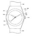
図11は、腕時計1000の正面図である。腕時計1000は、時計ケース1002と、時計ケース1002に連結された一対のバンド1003とを備えている。
時計ケース1002の正面には、上記各実施形態の電気泳動表示装置からなる表示部1005と、秒針1021と、分針1022と、時針1023とが設けられている。時計ケース1002の側面には、操作子としての竜頭1010と操作ボタン1011とが設けられている。竜頭1010は、ケース内部に設けられる巻真(図示は省略)に連結されており、巻真と一体となって多段階(例えば2段階)で押し引き自在、かつ、回転自在に設けられている。表示部1005では、背景となる画像、日付や時間などの文字列、あるいは秒針、分針、時針などを表示することができる。(Electronics)
Next, a case where the
FIG. 11 is a front view of the
On the front surface of the
図12は電子ペーパー1100の構成を示す斜視図である。電子ペーパー1100は、上記実施形態の電気泳動表示装置を表示領域1101に備えている。電子ペーパー1100は可撓性を有し、従来の紙と同様の質感及び柔軟性を有する書き換え可能なシートからなる本体1102を備えて構成されている。 FIG. 12 is a perspective view illustrating a configuration of the
図13は、電子ノート1200の構成を示す斜視図である。電子ノート1200は、上記の電子ペーパー1100が複数枚束ねられ、カバー1201に挟まれているものである。カバー1201は、例えば外部の装置から送られる表示データを入力する図示は省略の表示データ入力手段を備える。これにより、その表示データに応じて、電子ペーパーが束ねられた状態のまま、表示内容の変更や更新を行うことができる。 FIG. 13 is a perspective view showing the configuration of the
以上の腕時計1000、電子ペーパー1100、及び電子ノート1200によれば、本発明に係る電気泳動表示装置が採用されているので、簡素な構成で多階調表示を実現した表示手段を備えた電子機器となる。
なお、上記の電子機器は、本発明に係る電子機器を例示するものであって、本発明の技術範囲を限定するものではない。例えば、携帯電話、携帯用オーディオ機器などの電子機器の表示部にも、本発明に係る電気光学装置は好適に用いることができる。According to the
In addition, said electronic device illustrates the electronic device which concerns on this invention, Comprising: The technical scope of this invention is not limited. For example, the electro-optical device according to the present invention can be suitably used for a display portion of an electronic device such as a mobile phone or a portable audio device.
100 電気泳動表示装置、5 表示部、32 電気泳動素子、35 画素電極、35a 第1電極、35b 第2電極、37 共通電極(対向電極)、40,40A,40B,40C,40D,40E 画素、63 コントローラー(制御部)、66 第1走査線、67 第2走査線、68 データ線、71 電源線、Rb 黒表示領域、Rw 白表示領域、135 導電体突起部、350 絶縁膜、351,451 島状部、352,452,552 接続配線部、353 共通配線部、551 主電極部、553 帯電極、TR1 第1トランジスタ(第1スイッチング素子)、TR2 第2トランジスタ(第2スイッチング素子)、TR3 第3トランジスタ(第3スイッチング素子) 100 electrophoretic display device, 5 display unit, 32 electrophoretic element, 35 pixel electrode, 35a first electrode, 35b second electrode, 37 common electrode (counter electrode), 40, 40A, 40B, 40C, 40D, 40E pixel, 63 Controller (Control Unit), 66 First Scan Line, 67 Second Scan Line, 68 Data Line, 71 Power Line, Rb Black Display Area, Rw White Display Area, 135 Conductor Projection, 350 Insulating Film, 351, 451 Island-shaped part, 352, 452, 552 Connection wiring part, 353 Common wiring part, 551 Main electrode part, 553 Band electrode, TR1 First transistor (first switching element), TR2 Second transistor (second switching element), TR3 Third transistor (third switching element)
Claims (8)
Translated fromJapanese前記第1電極が前記画素の中央部に配置された平面視略正方形状の島状部と前記島状部から延びる接続配線部とを有し、前記第2電極が前記島状部の外縁に沿って形成されたCリング形状に形成され、
前記第1電極の前記接続配線部が、前記第2電極の前記Cリング形状の先端の開口部を経由して外側に引き出されており、
前記第1電極と前記第2電極との電位差により階調を表示することを特徴とする電気泳動表示装置。Will by sandwiching an electrophoretic element between a pair of substrates, and a second electrode formed on the first electrode andthe first electrode and the same layer which is formed for each pixel on one of the substrate, the other of the substrate An electrophoretic display device having a counter electrode formed and opposed to the first electrode and the second electrode via the electrophoretic element,
The first electrode includes an island-like portion having a substantially square shape in plan view disposed at a central portion of the pixel and a connection wiring portion extending from the island-like portion, and the second electrode is disposed on an outer edge of the island-like portion. Formed in a C-ring shape formed along,
The connection wiring portion of the first electrode is drawn to the outside via the opening at the tip of the C-ring shape of the second electrode;
An electrophoretic display device that displays gray scales by a potential difference between the first electrode and the second electrode.
Priority Applications (2)
| Application Number | Priority Date | Filing Date | Title |
|---|---|---|---|
| JP2009276411AJP5581677B2 (en) | 2009-12-04 | 2009-12-04 | Electrophoretic display device and electronic apparatus |
| US12/955,057US8928576B2 (en) | 2009-12-04 | 2010-11-29 | Electrophoretic display device, driving method thereof, and electronic apparatus |
Applications Claiming Priority (1)
| Application Number | Priority Date | Filing Date | Title |
|---|---|---|---|
| JP2009276411AJP5581677B2 (en) | 2009-12-04 | 2009-12-04 | Electrophoretic display device and electronic apparatus |
Publications (2)
| Publication Number | Publication Date |
|---|---|
| JP2011118216A JP2011118216A (en) | 2011-06-16 |
| JP5581677B2true JP5581677B2 (en) | 2014-09-03 |
Family
ID=44081594
Family Applications (1)
| Application Number | Title | Priority Date | Filing Date |
|---|---|---|---|
| JP2009276411AActiveJP5581677B2 (en) | 2009-12-04 | 2009-12-04 | Electrophoretic display device and electronic apparatus |
Country Status (2)
| Country | Link |
|---|---|
| US (1) | US8928576B2 (en) |
| JP (1) | JP5581677B2 (en) |
Families Citing this family (6)
| Publication number | Priority date | Publication date | Assignee | Title |
|---|---|---|---|---|
| WO2012176113A1 (en)* | 2011-06-22 | 2012-12-27 | Koninklijke Philips Electronics N.V. | Autostereoscopic display apparatus having optical magnification |
| CN102654980B (en)* | 2012-01-09 | 2015-01-14 | 京东方科技集团股份有限公司 | Electronic paper display device and driving method thereof |
| US9865195B2 (en)* | 2014-07-02 | 2018-01-09 | James Duane Bennett | Multimode electronic display |
| US10324577B2 (en)* | 2017-02-28 | 2019-06-18 | E Ink Corporation | Writeable electrophoretic displays including sensing circuits and styli configured to interact with sensing circuits |
| JP7446774B2 (en) | 2019-11-07 | 2024-03-11 | 株式会社ジャパンディスプレイ | Semiconductor substrates and display devices |
| US12190836B2 (en) | 2023-01-27 | 2025-01-07 | E Ink Corporation | Multi-element pixel electrode circuits for electro-optic displays and methods for driving the same |
Family Cites Families (18)
| Publication number | Priority date | Publication date | Assignee | Title |
|---|---|---|---|---|
| EP1196814A1 (en)* | 1999-07-21 | 2002-04-17 | E Ink Corporation | Use of a storage capacitor to enhance the performance of an active matrix driven electronic display |
| JP2004012829A (en)* | 2002-06-07 | 2004-01-15 | Canon Inc | Electrophoretic display |
| JP4416380B2 (en)* | 2002-06-14 | 2010-02-17 | キヤノン株式会社 | Electrophoretic display device and driving method thereof |
| US7271947B2 (en) | 2002-08-16 | 2007-09-18 | Sipix Imaging, Inc. | Electrophoretic display with dual-mode switching |
| TWI270835B (en)* | 2002-10-29 | 2007-01-11 | Matsushita Electric Industrial Co Ltd | Display device and generation method of image display particle |
| JP4522101B2 (en)* | 2004-01-27 | 2010-08-11 | キヤノン株式会社 | Electrophoretic display device and driving method of electrophoretic display device |
| JP4367386B2 (en)* | 2004-10-25 | 2009-11-18 | セイコーエプソン株式会社 | Electro-optical device, driving circuit thereof, driving method, and electronic apparatus |
| JP4419944B2 (en) | 2005-03-29 | 2010-02-24 | セイコーエプソン株式会社 | Electrophoretic display device and driving method thereof |
| FR2897224B1 (en)* | 2006-02-08 | 2009-01-16 | Realeyes3D Sa | METHOD FOR ENTRYING, ARCHIVING, CONSULTING AND TRANSMITTING A DOCUMENT TO A RECIPIENT USING A CAMERA |
| TWI344133B (en) | 2006-02-24 | 2011-06-21 | Prime View Int Co Ltd | Thin film transistor array substrate and electronic ink display device |
| JP4816245B2 (en)* | 2006-05-19 | 2011-11-16 | 株式会社日立製作所 | Electrophoretic display device |
| GB2447983A (en)* | 2007-03-30 | 2008-10-01 | Seiko Epson Corp | Electrochromic display apparatus and method for operating said display apparatus |
| JP2009204926A (en)* | 2008-02-28 | 2009-09-10 | Seiko Epson Corp | Method for manufacturing electrophoretic display device, electrophoretic display device and electronic equipment |
| JP2009229832A (en)* | 2008-03-24 | 2009-10-08 | Seiko Epson Corp | Method of driving electrophoretic display device, electrophoretic display device, and electronic apparatus |
| JP5262217B2 (en)* | 2008-03-24 | 2013-08-14 | セイコーエプソン株式会社 | Voltage selection circuit, electrophoretic display device, and electronic device |
| KR20100004031A (en)* | 2008-07-02 | 2010-01-12 | 삼성전자주식회사 | Transparent display device and manufacturing method thereof |
| JP2010102299A (en)* | 2008-09-25 | 2010-05-06 | Seiko Epson Corp | Electrophoretic display device, method of driving same, and electronic apparatus |
| KR101631454B1 (en)* | 2008-10-31 | 2016-06-17 | 가부시키가이샤 한도오따이 에네루기 켄큐쇼 | Logic circuit |
- 2009
- 2009-12-04JPJP2009276411Apatent/JP5581677B2/enactiveActive
- 2010
- 2010-11-29USUS12/955,057patent/US8928576B2/enactiveActive
Also Published As
| Publication number | Publication date |
|---|---|
| US20110134156A1 (en) | 2011-06-09 |
| JP2011118216A (en) | 2011-06-16 |
| US8928576B2 (en) | 2015-01-06 |
Similar Documents
| Publication | Publication Date | Title |
|---|---|---|
| JP5200700B2 (en) | Electrophoretic display device and electronic apparatus | |
| JP5504567B2 (en) | Electrophoretic display device driving method, electrophoretic display device, and electronic apparatus | |
| JP5428211B2 (en) | Driving method of electrophoretic display device | |
| JP5581677B2 (en) | Electrophoretic display device and electronic apparatus | |
| JP5338622B2 (en) | Electrophoretic display device driving method, electrophoretic display device, and electronic apparatus | |
| US8355193B2 (en) | Electrophoretic display device and electronic apparatus | |
| JP2011221097A (en) | Substrate for electrophoretic display device, electrophoretic display device and electronic apparatus | |
| US20110170169A1 (en) | Electrophoretic display device and electronic apparatus | |
| JP2011123216A (en) | Method of driving electrophoretic display device, electrophoretic display device and electronic equipment | |
| JP2011128272A (en) | Electrophoretic display device, driving method of electrophoretic display device, and electronic device | |
| EP2133740A2 (en) | Electrophoretic display device, electronic apparatus, and method of driving electrophoretic display device | |
| JP5375007B2 (en) | Matrix device drive circuit, matrix device, image display device, electrophoretic display device, and electronic apparatus | |
| CN103137078B (en) | Display device and method for controlling display device | |
| KR20090101842A (en) | Driving circuit for electrophoretic display device, electrophoretic display device, method for driving the same, and electronic apparatus | |
| US20100085343A1 (en) | Electrophoretic display, electronic apparatus, and method for driving electrophoretic display | |
| JP2011123282A (en) | Method for driving electrophoretic display device, electrophoretic display device, and electronic device | |
| JP2011095564A (en) | Electrophoretic display device, driving method of the same, and electronic apparatus | |
| JP2011095565A (en) | Electrophoretic display device and method of driving the same, and electronic apparatus | |
| JP2010096915A (en) | Method for driving electrophoretic display, electrophoretic display, and electronic equipment | |
| JP2011145390A (en) | Electrophoretic display device and electronic equipment | |
| JP5286973B2 (en) | Electrophoretic display device, driving method thereof, and electronic apparatus | |
| JP5262539B2 (en) | Electrophoretic display device and electronic apparatus | |
| JP2011180360A (en) | Electrophoretic display apparatus, and electronic device | |
| JP2013152260A (en) | Electro-optical apparatus | |
| JP5527128B2 (en) | Electrophoretic display device driving method, electrophoretic display device, control circuit for electrophoretic display device, electronic apparatus |
Legal Events
| Date | Code | Title | Description |
|---|---|---|---|
| RD04 | Notification of resignation of power of attorney | Free format text:JAPANESE INTERMEDIATE CODE: A7424 Effective date:20120201 | |
| A621 | Written request for application examination | Free format text:JAPANESE INTERMEDIATE CODE: A621 Effective date:20121129 | |
| A977 | Report on retrieval | Free format text:JAPANESE INTERMEDIATE CODE: A971007 Effective date:20130612 | |
| A131 | Notification of reasons for refusal | Free format text:JAPANESE INTERMEDIATE CODE: A131 Effective date:20130806 | |
| A521 | Request for written amendment filed | Free format text:JAPANESE INTERMEDIATE CODE: A523 Effective date:20131007 | |
| A131 | Notification of reasons for refusal | Free format text:JAPANESE INTERMEDIATE CODE: A131 Effective date:20140304 | |
| A521 | Request for written amendment filed | Free format text:JAPANESE INTERMEDIATE CODE: A523 Effective date:20140424 | |
| A131 | Notification of reasons for refusal | Free format text:JAPANESE INTERMEDIATE CODE: A131 Effective date:20140520 | |
| A521 | Request for written amendment filed | Free format text:JAPANESE INTERMEDIATE CODE: A523 Effective date:20140529 | |
| TRDD | Decision of grant or rejection written | ||
| A01 | Written decision to grant a patent or to grant a registration (utility model) | Free format text:JAPANESE INTERMEDIATE CODE: A01 Effective date:20140617 | |
| A61 | First payment of annual fees (during grant procedure) | Free format text:JAPANESE INTERMEDIATE CODE: A61 Effective date:20140630 | |
| R150 | Certificate of patent or registration of utility model | Ref document number:5581677 Country of ref document:JP Free format text:JAPANESE INTERMEDIATE CODE: R150 | |
| S531 | Written request for registration of change of domicile | Free format text:JAPANESE INTERMEDIATE CODE: R313531 | |
| R350 | Written notification of registration of transfer | Free format text:JAPANESE INTERMEDIATE CODE: R350 | |
| S111 | Request for change of ownership or part of ownership | Free format text:JAPANESE INTERMEDIATE CODE: R313113 | |
| R350 | Written notification of registration of transfer | Free format text:JAPANESE INTERMEDIATE CODE: R350 | |
| R250 | Receipt of annual fees | Free format text:JAPANESE INTERMEDIATE CODE: R250 | |
| R250 | Receipt of annual fees | Free format text:JAPANESE INTERMEDIATE CODE: R250 | |
| R250 | Receipt of annual fees | Free format text:JAPANESE INTERMEDIATE CODE: R250 | |
| R250 | Receipt of annual fees | Free format text:JAPANESE INTERMEDIATE CODE: R250 | |
| R250 | Receipt of annual fees | Free format text:JAPANESE INTERMEDIATE CODE: R250 | |
| R250 | Receipt of annual fees | Free format text:JAPANESE INTERMEDIATE CODE: R250 | |
| R250 | Receipt of annual fees | Free format text:JAPANESE INTERMEDIATE CODE: R250 |