JP5581263B2 - Buffer circuit - Google Patents
Buffer circuitDownload PDFInfo
- Publication number
- JP5581263B2 JP5581263B2JP2011104103AJP2011104103AJP5581263B2JP 5581263 B2JP5581263 B2JP 5581263B2JP 2011104103 AJP2011104103 AJP 2011104103AJP 2011104103 AJP2011104103 AJP 2011104103AJP 5581263 B2JP5581263 B2JP 5581263B2
- Authority
- JP
- Japan
- Prior art keywords
- transistor
- terminal
- buffer circuit
- gain
- potential side
- Prior art date
- Legal status (The legal status is an assumption and is not a legal conclusion. Google has not performed a legal analysis and makes no representation as to the accuracy of the status listed.)
- Active
Links
Images
Classifications
- H—ELECTRICITY
- H03—ELECTRONIC CIRCUITRY
- H03K—PULSE TECHNIQUE
- H03K19/00—Logic circuits, i.e. having at least two inputs acting on one output; Inverting circuits
- H03K19/0175—Coupling arrangements; Interface arrangements
- H03K19/0185—Coupling arrangements; Interface arrangements using field effect transistors only
- H03K19/018507—Interface arrangements
- H03K19/018521—Interface arrangements of complementary type, e.g. CMOS
- G—PHYSICS
- G09—EDUCATION; CRYPTOGRAPHY; DISPLAY; ADVERTISING; SEALS
- G09G—ARRANGEMENTS OR CIRCUITS FOR CONTROL OF INDICATING DEVICES USING STATIC MEANS TO PRESENT VARIABLE INFORMATION
- G09G5/00—Control arrangements or circuits for visual indicators common to cathode-ray tube indicators and other visual indicators
- H—ELECTRICITY
- H03—ELECTRONIC CIRCUITRY
- H03K—PULSE TECHNIQUE
- H03K17/00—Electronic switching or gating, i.e. not by contact-making and –breaking
- H03K17/06—Modifications for ensuring a fully conducting state
- H—ELECTRICITY
- H03—ELECTRONIC CIRCUITRY
- H03K—PULSE TECHNIQUE
- H03K17/00—Electronic switching or gating, i.e. not by contact-making and –breaking
- H03K17/16—Modifications for eliminating interference voltages or currents
- H—ELECTRICITY
- H03—ELECTRONIC CIRCUITRY
- H03K—PULSE TECHNIQUE
- H03K17/00—Electronic switching or gating, i.e. not by contact-making and –breaking
- H03K17/51—Electronic switching or gating, i.e. not by contact-making and –breaking characterised by the components used
- H03K17/56—Electronic switching or gating, i.e. not by contact-making and –breaking characterised by the components used by the use, as active elements, of semiconductor devices
- H03K17/687—Electronic switching or gating, i.e. not by contact-making and –breaking characterised by the components used by the use, as active elements, of semiconductor devices the devices being field-effect transistors
- H—ELECTRICITY
- H03—ELECTRONIC CIRCUITRY
- H03K—PULSE TECHNIQUE
- H03K19/00—Logic circuits, i.e. having at least two inputs acting on one output; Inverting circuits
- H03K19/0175—Coupling arrangements; Interface arrangements
- H—ELECTRICITY
- H03—ELECTRONIC CIRCUITRY
- H03K—PULSE TECHNIQUE
- H03K3/00—Circuits for generating electric pulses; Monostable, bistable or multistable circuits
- G—PHYSICS
- G09—EDUCATION; CRYPTOGRAPHY; DISPLAY; ADVERTISING; SEALS
- G09G—ARRANGEMENTS OR CIRCUITS FOR CONTROL OF INDICATING DEVICES USING STATIC MEANS TO PRESENT VARIABLE INFORMATION
- G09G2310/00—Command of the display device
- G09G2310/02—Addressing, scanning or driving the display screen or processing steps related thereto
- G09G2310/0264—Details of driving circuits
- G09G2310/0291—Details of output amplifiers or buffers arranged for use in a driving circuit
Landscapes
- Engineering & Computer Science (AREA)
- Computer Hardware Design (AREA)
- Physics & Mathematics (AREA)
- Computing Systems (AREA)
- General Engineering & Computer Science (AREA)
- Mathematical Physics (AREA)
- General Physics & Mathematics (AREA)
- Theoretical Computer Science (AREA)
- Logic Circuits (AREA)
- Electronic Switches (AREA)
- Shift Register Type Memory (AREA)
Description
Translated fromJapanese本発明は、バッファ回路と該バッファ回路を応用した装置、電子機器などに関する。 The present invention relates to a buffer circuit, an apparatus to which the buffer circuit is applied, an electronic apparatus, and the like.
近年、液晶表示装置や発光装置などの表示装置が広く普及している。一方で、情報化社会の到来により、取り扱われる情報の絶対量が飛躍的に増加し、記憶装置などの開発も進められてきた。 In recent years, display devices such as liquid crystal display devices and light-emitting devices have become widespread. On the other hand, with the advent of the information society, the absolute amount of information handled has increased dramatically, and development of storage devices and the like has been promoted.
このような表示装置や記憶装置には、複数のトランジスタがマトリクス状に設けられている。マトリクス状に設けられた複数のトランジスタは、走査線により制御され、信号線によりデータが供給される。なお、このような同一基板上に形成されたトランジスタは、生産性の点から同一極性(単極性)であることが好ましい。 In such a display device or a memory device, a plurality of transistors are provided in a matrix. The plurality of transistors provided in a matrix are controlled by scanning lines, and data is supplied by signal lines. Note that the transistors formed over the same substrate are preferably of the same polarity (single polarity) from the viewpoint of productivity.
このようなトランジスタがマトリクス状に設けられた基板上において、走査線に供給される信号は、シフトレジスタ回路(例えば、特許文献1)やバッファ回路から供給される。 On a substrate provided with such transistors in a matrix, a signal supplied to the scan line is supplied from a shift register circuit (for example, Patent Document 1) or a buffer circuit.
しかし、従来の単極性のバッファ回路(例えば、図2に示されるもの)に設けられる、ソース及びドレインの一方が出力部に接続され、ソース及びドレインの他方が電源線(Nチャネル型トランジスタの場合は高電位側の電源線Vdd、Pチャネル型トランジスタの場合は低電位側の電源線Vss)に接続されたトランジスタは、該トランジスタ自体の利得を増大させると、バッファ回路としての利得を減少させる方向に作用する。However, in a conventional unipolar buffer circuit (for example, the one shown in FIG. 2), one of the source and the drain is connected to the output section, and the other of the source and the drain is a power line (in the case of an N-channel transistor). Is connected to the high-potential side power line Vdd , and in the case of a P-channel transistor, the transistor connected to the low-potential side power line Vss ) decreases the gain as the buffer circuit when the gain of the transistor itself increases. Acts in the direction of
なお、バッファ回路の利得を確保するためにはこのトランジスタのサイズを十分に大きくすることができず、このトランジスタから流れる電流値により出力部の電圧のスルーレートが決まるので、スルーレートを向上させることが困難であるという問題がある。 In order to secure the gain of the buffer circuit, the size of this transistor cannot be increased sufficiently, and the slew rate of the voltage at the output section is determined by the current value flowing from this transistor, so that the slew rate can be improved. There is a problem that is difficult.
なお、本明細書において、「スルーレート(Slew Rate)」とは、出力電圧を立ち上がり(Nチャネル型トランジスタ)または立ち下がり(Pチャネル型トランジスタ)に要した時間で除したものをいい、立ち上がり特性(Nチャネル型トランジスタ)または立ち下がり特性(Pチャネル型トランジスタ)とも呼ばれるものである。 In this specification, “slew rate” refers to the output voltage divided by the time required for rising (N-channel type transistor) or falling (P-channel type transistor). It is also called a (N-channel transistor) or a falling characteristic (P-channel transistor).
本発明の一態様は、スルーレートが高いバッファ回路を提供することを課題とする。 An object of one embodiment of the present invention is to provide a buffer circuit with a high slew rate.
更には、このようなスルーレートが高いバッファ回路を同一極性のトランジスタにより構成することを課題とする。バッファ回路内のトランジスタを同一極性(Nチャネル型トランジスタまたはPチャネル型トランジスタ)とすることで簡略な工程により作製することができ、生産性が高まるからである。 Furthermore, another object of the present invention is to construct such a buffer circuit having a high slew rate with transistors having the same polarity. This is because when the transistors in the buffer circuit have the same polarity (N-channel transistors or P-channel transistors), the transistors can be manufactured through a simple process and productivity is increased.
そして、上記課題を解決することが可能なバッファ回路を構成するに際し、可能な限り単純な構成とし、バッファ回路の占有面積を小さくすることをも課題とする。 When configuring a buffer circuit capable of solving the above-described problems, it is also an object to make the configuration as simple as possible and reduce the area occupied by the buffer circuit.
本発明の一態様では、バッファ回路のスルーレートを高めるために、駆動能力を向上させ、高周波成分の利得を向上させる。 In one embodiment of the present invention, in order to increase the slew rate of a buffer circuit, driving capability is improved and the gain of a high-frequency component is improved.
本発明の一態様であるバッファ回路は、少なくとも複数のトランジスタと、容量素子と、を有し、該バッファ回路の利得が、前記複数のトランジスタのすべての利得により決定されることを特徴とする。 A buffer circuit which is one embodiment of the present invention includes at least a plurality of transistors and a capacitor, and a gain of the buffer circuit is determined by all gains of the plurality of transistors.
本発明の一態様であるバッファ回路は、第1のトランジスタ乃至第6のトランジスタ、容量素子、入力部及び出力部を有し、第1のトランジスタの第1端子及び第1のトランジスタの第3端子は高電位側の電源線に接続され、第1のトランジスタの第2端子は第2のトランジスタの第1端子及び第3のトランジスタの第3端子に接続され、第2のトランジスタの第2端子は低電位側の電源線に接続され、第2のトランジスタの第3端子はバッファ回路の入力部に接続され、第3のトランジスタの第1端子は高電位側の電源線に接続され、第3のトランジスタの第2端子は第4のトランジスタの第1端子及び第5のトランジスタの第3端子に接続され、第4のトランジスタの第2端子は低電位側の電源線に接続され、第4のトランジスタの第3端子はバッファ回路の入力部に接続され、第5のトランジスタの第1端子は高電位側の電源線に接続され、第5のトランジスタの第2端子は第6のトランジスタの第1端子及びバッファ回路の出力部に接続され、第6のトランジスタの第2端子は低電位側の電源線に接続され、第6のトランジスタの第3端子はバッファ回路の入力部に接続され、前記第1のトランジスタの第2端子は容量素子を介してバッファ回路の出力部に接続され、前記第1のトランジスタ乃至第6のトランジスタはすべてNチャネル型トランジスタである。なお、高電位側の電源線は第1の配線と呼んでもよいし、低電位側の電源線は第2の配線と呼んでもよい。第1の配線及び第2の配線は一定の電位とするとよい。 A buffer circuit which is one embodiment of the present invention includes first to sixth transistors, a capacitor, an input portion, and an output portion, and includes a first terminal of the first transistor and a third terminal of the first transistor. Is connected to the power line on the high potential side, the second terminal of the first transistor is connected to the first terminal of the second transistor and the third terminal of the third transistor, and the second terminal of the second transistor is The third terminal of the second transistor is connected to the input portion of the buffer circuit, the first terminal of the third transistor is connected to the power line on the high potential side, and the third terminal of the second transistor is connected to the low potential side power line. The second terminal of the transistor is connected to the first terminal of the fourth transistor and the third terminal of the fifth transistor, the second terminal of the fourth transistor is connected to the power line on the low potential side, and the fourth transistor Third of The child is connected to the input portion of the buffer circuit, the first terminal of the fifth transistor is connected to the power supply line on the high potential side, the second terminal of the fifth transistor is the first terminal of the sixth transistor, and the buffer circuit The second terminal of the sixth transistor is connected to the power line on the low potential side, the third terminal of the sixth transistor is connected to the input part of the buffer circuit, The second terminal is connected to the output portion of the buffer circuit via a capacitive element, and the first to sixth transistors are all N-channel transistors. Note that the power line on the high potential side may be referred to as a first wiring, and the power line on the low potential side may be referred to as a second wiring. The first wiring and the second wiring are preferably set at a constant potential.
上記構成のバッファ回路において、前記第1のトランジスタ乃至第6のトランジスタはすべて酸化物半導体により設けられていることが好ましい。 In the buffer circuit having the above structure, it is preferable that all of the first to sixth transistors be formed using an oxide semiconductor.
本発明の一態様であるバッファ回路は、第1のトランジスタ乃至第6のトランジスタ、容量素子、入力部及び出力部を有し、第1のトランジスタの第1端子は高電位側の電源線に接続され、第1のトランジスタの第2端子は第2のトランジスタの第1端子及び第4のトランジスタの第3端子に接続され、第1のトランジスタの第3端子はバッファ回路の入力部に接続され、第2のトランジスタの第2端子及び第2のトランジスタの第3端子は低電位側の電源線に接続され、第3のトランジスタの第1端子は高電位側の電源線に接続され、第3のトランジスタの第2端子は第4のトランジスタの第1端子及び第6のトランジスタの第3端子に接続され、第3のトランジスタの第3端子はバッファ回路の入力部に接続され、第4のトランジスタの第2端子は低電位側の電源線に接続され、第5のトランジスタの第1端子は高電位側の電源線に接続され、第5のトランジスタの第2端子は第6のトランジスタの第1端子及びバッファ回路の出力部に接続され、第5のトランジスタの第3端子はバッファ回路の入力部に接続され、第6のトランジスタの第2端子は低電位側の電源線に接続され、前記第1のトランジスタの第2端子は容量素子を介してバッファ回路の出力部に接続され、前記第1のトランジスタ乃至第6のトランジスタはすべてPチャネル型トランジスタである。なお、高電位側の電源線は第1の配線と呼んでもよいし、低電位側の電源線は第2の配線と呼んでもよい。第1の配線及び第2の配線は一定の電位とするとよい。 A buffer circuit which is one embodiment of the present invention includes first to sixth transistors, a capacitor, an input portion, and an output portion, and a first terminal of the first transistor is connected to a power supply line on a high potential side The second terminal of the first transistor is connected to the first terminal of the second transistor and the third terminal of the fourth transistor; the third terminal of the first transistor is connected to the input of the buffer circuit; The second terminal of the second transistor and the third terminal of the second transistor are connected to the low-potential side power line, the first terminal of the third transistor is connected to the high-potential side power line, and the third terminal The second terminal of the transistor is connected to the first terminal of the fourth transistor and the third terminal of the sixth transistor. The third terminal of the third transistor is connected to the input portion of the buffer circuit. The second terminal is connected to the low-potential side power line, the first terminal of the fifth transistor is connected to the high-potential side power line, the second terminal of the fifth transistor is the first terminal of the sixth transistor, and Connected to the output of the buffer circuit, the third terminal of the fifth transistor is connected to the input of the buffer circuit, the second terminal of the sixth transistor is connected to the power line on the low potential side, and the first terminal The second terminal of the transistor is connected to the output portion of the buffer circuit through a capacitor, and the first to sixth transistors are all P-channel transistors. Note that the power line on the high potential side may be referred to as a first wiring, and the power line on the low potential side may be referred to as a second wiring. The first wiring and the second wiring are preferably set at a constant potential.
なお、本明細書において「第1端子」は、ソース及びドレインの一方を指し、「第2端子」は、ソース及びドレインの他方を指す。そして、「第3端子」は、ゲートを指す。 In this specification, the “first terminal” refers to one of a source and a drain, and the “second terminal” refers to the other of the source and the drain. The “third terminal” refers to the gate.
なお、本明細書において「利得」は、入力電圧に対する出力電圧の比である。 In this specification, “gain” is the ratio of the output voltage to the input voltage.
なお、本明細書において「駆動能力」は、出力負荷に電流を出力する能力である。 In the present specification, “drive capability” is the capability of outputting a current to the output load.
なお、本明細書において、「Nチャネル型トランジスタ」とは、ゲート電圧(ソースの電位に対するゲートの電位)が閾値電圧よりも高いときにオンするすべてのトランジスタをいう。「Pチャネル型トランジスタ」とは、ゲート電圧(ソースの電位に対するゲートの電位)が閾値電圧よりも低いときにオンするすべてのトランジスタをいう。従って、「Nチャネル型」または「Pチャネル型」という呼称は上記定義した事項以外の事柄を限定するものではない。 Note that in this specification, an “N-channel transistor” refers to all transistors that are turned on when a gate voltage (a gate potential with respect to a source potential) is higher than a threshold voltage. “P-channel transistor” refers to all transistors that are turned on when a gate voltage (a gate potential with respect to a source potential) is lower than a threshold voltage. Therefore, the designation of “N channel type” or “P channel type” does not limit matters other than those defined above.
なお、ここでスルーレートは、前記利得と前記駆動能力により決定されるものである。利得が大きくとも駆動能力が低いと、出力負荷(容量素子)に充電する時間を要する。一方で、駆動能力が高く、利得が小さい場合には、最終段のトランジスタのVgsを十分に大きくするために時間を要し、高い駆動能力を発揮するまでに時間を要することになる。従って、スルーレートを向上させるためには、利得を増大させ、且つ駆動能力を十分に高くする。Here, the slew rate is determined by the gain and the driving capability. Even if the gain is large, if the driving capability is low, it takes time to charge the output load (capacitance element). On the other hand, when the driving capability is high and the gain is small, it takes time to sufficiently increase Vgs of the transistor in the final stage, and it takes time until the high driving capability is exhibited. Therefore, in order to improve the slew rate, the gain is increased and the driving capability is sufficiently increased.
駆動能力が高く、高周波成分における利得が大きいバッファ回路を得ることができる。このようなバッファ回路はスルーレートも高いものとなる。 A buffer circuit having a high driving capability and a large gain in high frequency components can be obtained. Such a buffer circuit has a high slew rate.
更には、このようなスルーレートが高いバッファ回路を同一極性のトランジスタにより構成することが可能なため、簡略な工程により作製することができる。言い換えると、従来は困難であった同一極性のトランジスタのみで構成されるバッファ回路のスルーレートを向上させることを可能とする。 Furthermore, since such a buffer circuit with a high slew rate can be formed of transistors having the same polarity, it can be manufactured by a simple process. In other words, it is possible to improve the slew rate of a buffer circuit composed of only transistors with the same polarity, which has been difficult in the prior art.
そして、上記効果を有するバッファ回路を可能な限り単純な構成とし、バッファ回路の占有面積を小さくすることも可能である。 It is also possible to make the buffer circuit having the above effects as simple as possible and reduce the area occupied by the buffer circuit.
以下では、本発明の実施の形態について図面を用いて詳細に説明する。ただし、本発明は以下の説明に限定されず、本発明の趣旨及びその範囲から逸脱することなくその形態及び詳細を様々に変更し得ることは、当業者であれば容易に理解される。したがって、本発明は、以下に示す実施の形態の記載内容に限定して解釈されるものではない。 Hereinafter, embodiments of the present invention will be described in detail with reference to the drawings. However, the present invention is not limited to the following description, and it will be easily understood by those skilled in the art that modes and details can be variously changed without departing from the spirit and scope of the present invention. Therefore, the present invention should not be construed as being limited to the description of the embodiments below.
(実施の形態1)
本実施の形態では、Nチャネル型トランジスタを用いて構成された本発明の一態様であるバッファ回路について説明する。(Embodiment 1)
In this embodiment, a buffer circuit which is one embodiment of the present invention including an N-channel transistor will be described.
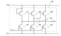
図1は、本発明の一態様であるバッファ回路100を示す図である。 FIG. 1 illustrates a
図1に示すバッファ回路100は、第1のトランジスタ乃至第6のトランジスタ、容量素子、入力部及び出力部を有し、第1のトランジスタ101では、第1端子及び第3端子が高電位側の電源線Vddに接続され、第2端子が第2のトランジスタ102の第1端子及び第3のトランジスタ103の第3端子に接続され、第2のトランジスタ102では、第2端子が低電位側の電源線Vssに接続され、第3端子がバッファ回路100の入力部Vinに接続され、第3のトランジスタ103では、第1端子が高電位側の電源線Vddに接続され、第2端子が第4のトランジスタ104の第1端子及び第5のトランジスタ105の第3端子に接続され、第4のトランジスタ104では、第2端子が低電位側の電源線Vssに接続され、第3端子がバッファ回路100の入力部Vinに接続され、第5のトランジスタ105では、第1端子が高電位側の電源線Vddに接続され、第2端子が第6のトランジスタ106の第1端子及びバッファ回路100の出力部Voutに接続され、第6のトランジスタ106では、第2端子が低電位側の電源線Vssに接続され、第3端子がバッファ回路100の入力部Vinに接続され、第1のトランジスタ101の第2端子は、容量素子107を介して出力部Voutに接続されている。A
図1に示すバッファ回路100は、駆動能力が高く、高周波成分の利得を大きくすることができる。更には、図1に示すバッファ回路は、スルーレートも高いものとなる。更には、図1に示すバッファ回路100は、同一極性のトランジスタにより構成することが可能なため、簡略な工程により作製することができる。言い換えると、従来は困難であった同一極性のトランジスタのみで構成されるバッファ回路のスルーレートを向上させることを可能とする。そして、6のトランジスタと1の容量素子で構成することができるため、バッファ回路の占有面積は小さい。 The
ここで、第1のトランジスタ101の利得をg1、第2のトランジスタ102の利得をg2、第3のトランジスタ103の利得をg3、第4のトランジスタ104の利得をg4、第5のトランジスタ105の利得をg5、第6のトランジスタ106の利得をg6、入力信号の角周波数をs(=2πf(fは周波数))、容量素子107の静電容量をCで表すと、図1に示すバッファ回路100の利得は、以下の数式(1)で表される。Here, the gain of the

すなわち、高周波成分ではsが極めて大きい(g1、g5<<sC)ため、1/s=0とすると、高周波成分の利得は以下の数式(2)で表される。That is, since s is extremely large in the high frequency component (g1 , g5 << sC), when 1 / s = 0, the gain of the high frequency component is expressed by the following formula (2).
そして、低周波成分ではsが極めて小さい(g1、g5>>sC)ため、s=0とすると、低周波成分の利得は以下の数式(3)で表される。Since s is extremely small in the low frequency component (g1 , g5 >> sC), when s = 0, the gain of the low frequency component is expressed by the following formula (3).
ここで、上記数式(1)は次のように導出される。第1のトランジスタ101の第1端子と第2端子の間に流れる電流をI1とし、第3のトランジスタ103の第1端子と第2端子の間に流れる電流をI3とし、第5のトランジスタ105の第1端子と第2端子の間に流れる電流をI5とし、容量素子107の一方の電極と他方の電極の間に流れる電流をI7とすると、これらは以下の数式(4)〜(7)で表される。Here, the above formula (1) is derived as follows. The current flowing between the first terminal and the second terminal of the
なお、ここでVaは、第3のトランジスタ103の第3端子に接続されたノードの電位であり、Vbは、第5のトランジスタ105の第3端子に接続されたノードの電位である。上記数式(4)〜(7)を、VaとVbを含まないように解くことで上記数式(1)が導出される。Note that here, Va is a potential of a node connected to the third terminal of the
図1に示すバッファ回路100を用いることで、高周波成分の利得を大きくすることができる。これは、第5のトランジスタ105の利得を大きくすることで、高周波成分においてバッファ回路100の利得を増大させるためである。 By using the
ここで、本発明の一態様である図1に示すバッファ回路の技術的特徴を説明するために、他のバッファ回路について検討する。 Here, in order to describe the technical features of the buffer circuit illustrated in FIG. 1 which is one embodiment of the present invention, another buffer circuit is considered.
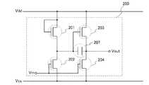
図2は、バッファ回路200を示す図である。 FIG. 2 is a diagram illustrating the
図2に示すバッファ回路200は、第1のトランジスタ乃至第4のトランジスタ、容量素子、入力部及び出力部を有し、第1のトランジスタ201では、第1端子及び第3端子が高電位側の電源線Vddに接続され、第2端子が第2のトランジスタ202の第1端子及び第3のトランジスタ203の第3端子に接続され、第2のトランジスタ202では、第2端子が低電位側の電源線Vssに接続され、第3端子がバッファ回路200の入力部Vinに接続され、第3のトランジスタ203では、第1端子が高電位側の電源線Vddに接続され、第2端子が第4のトランジスタ204の第1端子とバッファ回路200の出力部Voutに接続され、第4のトランジスタ204では、第2端子が低電位側の電源線Vssに接続され、第3端子がバッファ回路200の入力部Vinに接続され、第1のトランジスタ201の第2端子は、容量素子207を介して出力部Voutに接続されている。A
ここで、第1のトランジスタ201の利得をg1、第2のトランジスタ202の利得をg2、第3のトランジスタ203の利得をg3、第4のトランジスタ204の利得をg4、入力信号の角周波数をs(=2πf(fは周波数))、容量素子207の静電容量をCで表すと、図2に示すバッファ回路200の利得は、以下の数式(8)で表される。Here, the gain of the
すなわち、高周波成分ではsが極めて大きい(g1、g3<<sC)ため、1/s=0とすると、高周波成分の利得は以下の数式(9)で表される。That is, since s is extremely large in the high frequency component (g1 , g3 << sC), when 1 / s = 0, the gain of the high frequency component is expressed by the following formula (9).
そして、低周波成分ではsが極めて小さい(g1、g3>>sC)ため、s=0とすると、低周波成分の利得は以下の数式(10)で表される。Since s is extremely small in the low frequency component (g1 , g3 >> sC), when s = 0, the gain of the low frequency component is expressed by the following formula (10).
上記数式(9)には第3のトランジスタ203の利得が含まれず、図2のバッファ回路200では、第3のトランジスタ203の利得が高周波成分の利得の増大に寄与しない。すなわち、高電位側の電源線に接続された最終段のトランジスタが利得の増大に寄与しない。更には、上記数式(10)から、第3のトランジスタ203の利得を増大させると、バッファ回路の低周波成分での利得を減少させる方向に作用する。 The above formula (9) does not include the gain of the
一方で、図1に示すバッファ回路100では、高電位側の電源線Vddに接続された最終段のトランジスタが利得の増大に寄与するため、該トランジスタのチャネル長を大きくするなどして最終段のトランジスタの利得を増大させることでバッファ回路の利得を増大させることができる。On the other hand, in the
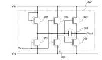
図3は、バッファ回路300を示す図である。 FIG. 3 is a diagram illustrating the
図3に示すバッファ回路300は、第1のトランジスタ乃至第6のトランジスタ、容量素子、入力部及び出力部を有し、第1のトランジスタ301では、第1端子及び第3端子が高電位側の電源線Vddに接続され、第2端子が第2のトランジスタ302の第1端子、第4のトランジスタ304の第3端子及び第5のトランジスタ305の第3端子に接続され、第2のトランジスタ302では、第2端子が低電位側の電源線Vssに接続され、第3端子は、バッファ回路300の入力部Vinに接続され、第3のトランジスタ303では、第1端子が高電位側の電源線Vddに接続され、第2端子が第4のトランジスタ304の第1端子と第6のトランジスタ306の第3端子に接続され、第3端子がバッファ回路300の入力部Vinに接続され、第4のトランジスタ304では、第2端子が低電位側の電源線Vssに接続され、第5のトランジスタ305では、第1端子が高電位側の電源線Vddに接続され、第2端子が第6のトランジスタ306の第1端子及びバッファ回路300の出力部Voutに接続され、第6のトランジスタ306では、第2端子が低電位側の電源線Vssに接続され、第1のトランジスタ301の第2端子は、容量素子307を介してバッファ回路300の出力部Voutに接続されている。A
ここで、第1のトランジスタ301の利得をg1、第2のトランジスタ302の利得をg2、第3のトランジスタ303の利得をg3、第4のトランジスタ304の利得をg4、第5のトランジスタ305の利得をg5、第6のトランジスタ306の利得をg6、入力信号の角周波数をs(=2πf(fは周波数))、容量素子307の静電容量をCで表すと、図3に示すバッファ回路300の高周波成分の利得は、以下の数式(11)で表される。Here, the gain of the
一方で、低周波成分の利得は、以下の数式(12)で表される。 On the other hand, the gain of the low frequency component is expressed by the following formula (12).
上記数式(11)には第5のトランジスタ305の利得が含まれず、図3のバッファ回路300では、第5のトランジスタ305の利得が高周波成分の利得の増大に寄与しない。すなわち、高電位側の電源線に接続された最終段のトランジスタが利得の増大に寄与しないことになる。一方で、上述したように、図1に示すバッファ回路100では、高電位側の電源線に接続された最終段のトランジスタが利得の増大に寄与するため、該トランジスタのチャネル長を大きくするなどして最終段のトランジスタの利得を増大させることでバッファ回路の利得を増大させることができる。 The above formula (11) does not include the gain of the
以上本実施の形態にて説明したように、本発明の一態様である図1に示すバッファ回路は、新しく、従来のバッファ回路に対して有利な効果を有するものである。このバッファ回路は表示装置の駆動回路に用いることができ、バッファ回路と画素部とを同一の基板上に形成することもできる。 As described above in this embodiment, the buffer circuit illustrated in FIG. 1 which is one embodiment of the present invention is new and has an advantageous effect over the conventional buffer circuit. This buffer circuit can be used for a driver circuit of a display device, and the buffer circuit and the pixel portion can be formed over the same substrate.
(実施の形態2)
本実施の形態では、Pチャネル型トランジスタを用いて構成された本発明の一態様であるバッファ回路について説明する。(Embodiment 2)
In this embodiment, a buffer circuit which is formed using a P-channel transistor and is one embodiment of the present invention will be described.
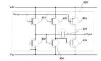
図4は、本発明の一態様であるバッファ回路400を示す図である。 FIG. 4 illustrates a
図4に示すバッファ回路400は、第1のトランジスタ乃至第6のトランジスタ、容量素子、入力部及び出力部を有し、第1のトランジスタ401では、第1端子が高電位側の電源線Vddに接続され、第2端子が第2のトランジスタ402の第1端子及び第4のトランジスタ404の第3端子に接続され、第3端子がバッファ回路400の入力部Vinに接続され、第2のトランジスタ402では、第2端子及び第3端子が低電位側の電源線Vssに接続され、第3のトランジスタ403では、第1端子が高電位側の電源線Vddに接続され、第2端子が第4のトランジスタ404の第1端子及び第6のトランジスタ406の第3端子に接続され、第3端子がバッファ回路400の入力部Vinに接続され、第4のトランジスタ404では、第2端子が低電位側の電源線Vssに接続され、第5のトランジスタ405では、第1端子が高電位側の電源線Vddに接続され、第2端子が第6のトランジスタ406の第1端子及びバッファ回路の出力部Voutに接続され、第3端子がバッファ回路400の入力部Vinに接続され、第6のトランジスタ406では、第2端子が低電位側の電源線Vssに接続され、第1のトランジスタ401の第2端子は、容量素子407を介して出力部Voutに接続されている。A
図4に示すバッファ回路400は、駆動能力が高く、高周波成分の利得を大きくすることができる。更には、このようなバッファ回路は、スルーレートも高いものとなる。更には、同一極性のトランジスタにより構成することが可能なため、簡略な工程により作製することができる。言い換えると、従来は困難であった同一極性のトランジスタのみで構成されるバッファ回路のスルーレートを高くすることを可能とする。そして、6のトランジスタと1の容量素子で構成することができるため、バッファ回路の占有面積を小さくすることも可能である。 The
以上本実施の形態にて説明したように、本発明の一態様である図4に示すバッファ回路は、新しく、従来のバッファ回路に対して有利な効果を有するものである。このバッファ回路は表示装置の駆動回路に用いることができ、バッファ回路と画素部とを同一の基板上に形成することもできる。 As described above in this embodiment, the buffer circuit illustrated in FIG. 4 which is one embodiment of the present invention is new and has an advantageous effect over the conventional buffer circuit. This buffer circuit can be used for a driver circuit of a display device, and the buffer circuit and the pixel portion can be formed over the same substrate.
100 バッファ回路
101 第1のトランジスタ
102 第2のトランジスタ
103 第3のトランジスタ
104 第4のトランジスタ
105 第5のトランジスタ
106 第6のトランジスタ
107 容量素子
200 バッファ回路
201 第1のトランジスタ
202 第2のトランジスタ
203 第3のトランジスタ
204 第4のトランジスタ
207 容量素子
300 バッファ回路
301 第1のトランジスタ
302 第2のトランジスタ
303 第3のトランジスタ
304 第4のトランジスタ
305 第5のトランジスタ
306 第6のトランジスタ
307 容量素子
400 バッファ回路
401 第1のトランジスタ
402 第2のトランジスタ
403 第3のトランジスタ
404 第4のトランジスタ
405 第5のトランジスタ
406 第6のトランジスタ
407 容量素子100
Claims (2)
Translated fromJapanese前記第1のトランジスタのゲートは、第1の配線に電気的に接続され、A gate of the first transistor is electrically connected to a first wiring;
前記第1のトランジスタのソース又はドレインの一方は、前記第1の配線に電気的に接続され、One of a source and a drain of the first transistor is electrically connected to the first wiring;
前記第1のトランジスタのソース又はドレインの他方は、前記第2のトランジスタのソース又はドレインの一方と電気的に接続され、The other of the source and the drain of the first transistor is electrically connected to one of the source and the drain of the second transistor;
前記第2のトランジスタのゲートは、入力端子と電気的に接続され、A gate of the second transistor is electrically connected to an input terminal;
前記第2のトランジスタのソース又はドレインの他方は、第2の配線と電気的に接続され、The other of the source and the drain of the second transistor is electrically connected to the second wiring;
前記第3のトランジスタのゲートは、前記第2のトランジスタのソース又はドレインの一方と電気的に接続され、A gate of the third transistor is electrically connected to one of a source and a drain of the second transistor;
前記第3のトランジスタのソース又はドレインの一方は、前記第1の配線と電気的に接続され、One of a source and a drain of the third transistor is electrically connected to the first wiring;
前記第3のトランジスタのソース又はドレインの他方は、前記第4のトランジスタのソース又はドレインの一方と電気的に接続され、The other of the source and the drain of the third transistor is electrically connected to one of the source and the drain of the fourth transistor;
前記第4のトランジスタのゲートは、前記入力端子と電気的に接続され、A gate of the fourth transistor is electrically connected to the input terminal;
前記第4のトランジスタのソース又はドレインの他方は、前記第2の配線と電気的に接続され、The other of the source and the drain of the fourth transistor is electrically connected to the second wiring;
前記第5のトランジスタのゲートは、前記第3のトランジスタのソース又はドレインの他方と電気的に接続され、A gate of the fifth transistor is electrically connected to the other of the source and the drain of the third transistor;
前記第5のトランジスタのソース又はドレインの一方は、前記第1の配線と電気的に接続され、One of a source and a drain of the fifth transistor is electrically connected to the first wiring;
前記第5のトランジスタのソース又はドレインの他方は、出力端子と電気的に接続され、The other of the source and the drain of the fifth transistor is electrically connected to the output terminal;
前記第6のトランジスタのゲートは、前記入力端子と電気的に接続され、A gate of the sixth transistor is electrically connected to the input terminal;
前記第6のトランジスタのソース又はドレインの一方は、前記出力端子と電気的に接続され、One of a source and a drain of the sixth transistor is electrically connected to the output terminal;
前記第6のトランジスタのソース又はドレインの他方は、前記第2の配線と電気的に接続され、The other of the source and the drain of the sixth transistor is electrically connected to the second wiring;
前記容量素子の一対の電極のうちの一方は、前記第1のトランジスタのソース又はドレインの他方と電気的に接続され、One of the pair of electrodes of the capacitor is electrically connected to the other of the source and the drain of the first transistor,
前記容量素子の一対の電極のうちの他方は、前記第5のトランジスタのソース又はドレインの他方と電気的に接続され、The other of the pair of electrodes of the capacitor is electrically connected to the other of the source and the drain of the fifth transistor,
前記第1の配線は、第1の電位を供給することができる機能を有し、The first wiring has a function of supplying a first potential;
前記第2の配線は、第2の電位を供給することができる機能を有し、The second wiring has a function of supplying a second potential,
前記第1の電位は、前記第2の電位よりも高く、The first potential is higher than the second potential;
前記第1のトランジスタと、前記第2のトランジスタと、前記第3のトランジスタと、前記第4のトランジスタと、前記第5のトランジスタと、前記第6のトランジスタと、はNチャネル型トランジスタであることを特徴とするバッファ回路。The first transistor, the second transistor, the third transistor, the fourth transistor, the fifth transistor, and the sixth transistor are N-channel transistors. A buffer circuit characterized by the above.
前記第1のトランジスタは、酸化物半導体を有し、The first transistor includes an oxide semiconductor;
前記第2のトランジスタは、酸化物半導体を有し、The second transistor includes an oxide semiconductor,
前記第3のトランジスタは、酸化物半導体を有し、The third transistor includes an oxide semiconductor;
前記第4のトランジスタは、酸化物半導体を有し、The fourth transistor includes an oxide semiconductor;
前記第5のトランジスタは、酸化物半導体を有し、The fifth transistor includes an oxide semiconductor;
前記第6のトランジスタは、酸化物半導体を有することを特徴とするバッファ回路。The buffer circuit is characterized in that the sixth transistor includes an oxide semiconductor.
Priority Applications (1)
| Application Number | Priority Date | Filing Date | Title |
|---|---|---|---|
| JP2011104103AJP5581263B2 (en) | 2010-05-13 | 2011-05-09 | Buffer circuit |
Applications Claiming Priority (3)
| Application Number | Priority Date | Filing Date | Title |
|---|---|---|---|
| JP2010110995 | 2010-05-13 | ||
| JP2010110995 | 2010-05-13 | ||
| JP2011104103AJP5581263B2 (en) | 2010-05-13 | 2011-05-09 | Buffer circuit |
Related Child Applications (1)
| Application Number | Title | Priority Date | Filing Date |
|---|---|---|---|
| JP2014141941ADivisionJP5723469B2 (en) | 2010-05-13 | 2014-07-10 | Buffer circuit |
Publications (3)
| Publication Number | Publication Date |
|---|---|
| JP2011259418A JP2011259418A (en) | 2011-12-22 |
| JP2011259418A5 JP2011259418A5 (en) | 2014-04-03 |
| JP5581263B2true JP5581263B2 (en) | 2014-08-27 |
Family
ID=44911374
Family Applications (2)
| Application Number | Title | Priority Date | Filing Date |
|---|---|---|---|
| JP2011104103AActiveJP5581263B2 (en) | 2010-05-13 | 2011-05-09 | Buffer circuit |
| JP2014141941AActiveJP5723469B2 (en) | 2010-05-13 | 2014-07-10 | Buffer circuit |
Family Applications After (1)
| Application Number | Title | Priority Date | Filing Date |
|---|---|---|---|
| JP2014141941AActiveJP5723469B2 (en) | 2010-05-13 | 2014-07-10 | Buffer circuit |
Country Status (3)
| Country | Link |
|---|---|
| US (1) | US8648849B2 (en) |
| JP (2) | JP5581263B2 (en) |
| KR (1) | KR101736075B1 (en) |
Families Citing this family (9)
| Publication number | Priority date | Publication date | Assignee | Title |
|---|---|---|---|---|
| US7432737B2 (en)* | 2005-12-28 | 2008-10-07 | Semiconductor Energy Laboratory Co., Ltd. | Semiconductor device, display device, and electronic device |
| US8154322B2 (en)* | 2009-12-21 | 2012-04-10 | Analog Devices, Inc. | Apparatus and method for HDMI transmission |
| US9466618B2 (en) | 2011-05-13 | 2016-10-11 | Semiconductor Energy Laboratory Co., Ltd. | Semiconductor device including two thin film transistors and method of manufacturing the same |
| US9742378B2 (en) | 2012-06-29 | 2017-08-22 | Semiconductor Energy Laboratory Co., Ltd. | Pulse output circuit and semiconductor device |
| JP6475424B2 (en) | 2013-06-05 | 2019-02-27 | 株式会社半導体エネルギー研究所 | Semiconductor device |
| KR20150141340A (en) | 2014-06-10 | 2015-12-18 | 삼성전자주식회사 | Devices having channel buffer block |
| US10824279B2 (en)* | 2015-02-06 | 2020-11-03 | Apple Inc. | Remote feedback tapping for a touch sensor panel driving circuit |
| CN108122529B (en)* | 2018-01-25 | 2021-08-17 | 京东方科技集团股份有限公司 | Gate driving unit, driving method thereof, and gate driving circuit |
| CN111613184B (en)* | 2020-06-22 | 2021-10-08 | 京东方科技集团股份有限公司 | Source driver circuit and display device |
Family Cites Families (18)
| Publication number | Priority date | Publication date | Assignee | Title |
|---|---|---|---|---|
| JPS55112038A (en)* | 1979-02-20 | 1980-08-29 | Mitsubishi Electric Corp | Bootstrap-type circuit |
| JPS55156427A (en)* | 1979-05-23 | 1980-12-05 | Sharp Corp | Bootstrap buffer circuit |
| US4500799A (en)* | 1980-07-28 | 1985-02-19 | Inmos Corporation | Bootstrap driver circuits for an MOS memory |
| JPS59231916A (en)* | 1983-06-15 | 1984-12-26 | Nec Corp | Semiconductor circuit |
| JP2737444B2 (en)* | 1991-04-30 | 1998-04-08 | 日本電気株式会社 | High-speed logic circuit |
| JPH05224629A (en)* | 1992-02-18 | 1993-09-03 | Sharp Corp | Driving circuit for active matrix display device |
| JP4785271B2 (en) | 2001-04-27 | 2011-10-05 | 株式会社半導体エネルギー研究所 | Liquid crystal display device, electronic equipment |
| JP4439761B2 (en) | 2001-05-11 | 2010-03-24 | 株式会社半導体エネルギー研究所 | Liquid crystal display device, electronic equipment |
| TW582005B (en) | 2001-05-29 | 2004-04-01 | Semiconductor Energy Lab | Pulse output circuit, shift register, and display device |
| US6788108B2 (en) | 2001-07-30 | 2004-09-07 | Semiconductor Energy Laboratory Co., Ltd. | Semiconductor device |
| JP4339103B2 (en) | 2002-12-25 | 2009-10-07 | 株式会社半導体エネルギー研究所 | Semiconductor device and display device |
| KR100490623B1 (en)* | 2003-02-24 | 2005-05-17 | 삼성에스디아이 주식회사 | Buffer circuit and active matrix display device using the same |
| JP5064747B2 (en)* | 2005-09-29 | 2012-10-31 | 株式会社半導体エネルギー研究所 | Semiconductor device, electrophoretic display device, display module, electronic device, and method for manufacturing semiconductor device |
| US7432737B2 (en) | 2005-12-28 | 2008-10-07 | Semiconductor Energy Laboratory Co., Ltd. | Semiconductor device, display device, and electronic device |
| EP1895545B1 (en)* | 2006-08-31 | 2014-04-23 | Semiconductor Energy Laboratory Co., Ltd. | Liquid crystal display device |
| JP5057828B2 (en)* | 2007-04-16 | 2012-10-24 | 株式会社ジャパンディスプレイイースト | Display device |
| JP2009188748A (en)* | 2008-02-06 | 2009-08-20 | Sony Corp | Inverter circuit, shift register circuit, nor circuit, and nand circuit |
| JP5106186B2 (en)* | 2008-03-13 | 2012-12-26 | 三菱電機株式会社 | Driver circuit |
- 2011
- 2011-05-09JPJP2011104103Apatent/JP5581263B2/enactiveActive
- 2011-05-10USUS13/104,494patent/US8648849B2/enactiveActive
- 2011-05-12KRKR1020110044399Apatent/KR101736075B1/enactiveActive
- 2014
- 2014-07-10JPJP2014141941Apatent/JP5723469B2/enactiveActive
Also Published As
| Publication number | Publication date |
|---|---|
| JP2014209788A (en) | 2014-11-06 |
| KR20110125597A (en) | 2011-11-21 |
| JP2011259418A (en) | 2011-12-22 |
| US8648849B2 (en) | 2014-02-11 |
| KR101736075B1 (en) | 2017-05-16 |
| US20110279438A1 (en) | 2011-11-17 |
| JP5723469B2 (en) | 2015-05-27 |
Similar Documents
| Publication | Publication Date | Title |
|---|---|---|
| JP5581263B2 (en) | Buffer circuit | |
| JP6683407B2 (en) | Overcurrent protection circuit for row display circuit of display panel and its array substrate | |
| US20250148999A1 (en) | Electronic device | |
| CN102419961B (en) | Semiconductor device | |
| US7863982B2 (en) | Driving circuit capable of enhancing response speed and related method | |
| CN103646636B (en) | Shift register, gate driver circuit and display device | |
| CN104809979B (en) | A kind of phase inverter and driving method, GOA unit, GOA circuits and display device | |
| JP4583933B2 (en) | Shift register and driving method thereof | |
| CN103299547B (en) | Level shifters, inverter circuits, and shift registers | |
| CN103247275A (en) | Shifting register unit, grid drive circuit and array substrate | |
| CN104282279A (en) | Shifting register unit, sifting register, gate drive circuit and displaying device | |
| US10074326B2 (en) | Electronic circuit, scanning circuit, display device, and electronic circuit life extending method | |
| CN106057118A (en) | Shifting register unit and driving method thereof, gate driving circuit and display device | |
| CN104992673A (en) | Inverter, gate driving circuit and display device | |
| JP4860765B2 (en) | Semiconductor device and electronic equipment | |
| JP5493023B2 (en) | Display device | |
| JP5719956B2 (en) | Display device | |
| KR20130096495A (en) | Buffer circuit for use in semiconductor device | |
| CN105845097A (en) | Shift register unit, driving method of shift register unit, gate drive circuit and display device | |
| CN106571121A (en) | Common electrode voltage generating circuit | |
| JP6167133B2 (en) | Display device | |
| JP5847969B2 (en) | Display device | |
| CN117037665B (en) | Scan driving circuit and display panel | |
| JP5690870B2 (en) | Display device | |
| JP6628837B2 (en) | Electronics |
Legal Events
| Date | Code | Title | Description |
|---|---|---|---|
| A521 | Request for written amendment filed | Free format text:JAPANESE INTERMEDIATE CODE: A523 Effective date:20140214 | |
| A621 | Written request for application examination | Free format text:JAPANESE INTERMEDIATE CODE: A621 Effective date:20140214 | |
| A977 | Report on retrieval | Free format text:JAPANESE INTERMEDIATE CODE: A971007 Effective date:20140627 | |
| TRDD | Decision of grant or rejection written | ||
| A01 | Written decision to grant a patent or to grant a registration (utility model) | Free format text:JAPANESE INTERMEDIATE CODE: A01 Effective date:20140708 | |
| A61 | First payment of annual fees (during grant procedure) | Free format text:JAPANESE INTERMEDIATE CODE: A61 Effective date:20140714 | |
| R150 | Certificate of patent or registration of utility model | Ref document number:5581263 Country of ref document:JP Free format text:JAPANESE INTERMEDIATE CODE: R150 | |
| R250 | Receipt of annual fees | Free format text:JAPANESE INTERMEDIATE CODE: R250 | |
| R250 | Receipt of annual fees | Free format text:JAPANESE INTERMEDIATE CODE: R250 | |
| R250 | Receipt of annual fees | Free format text:JAPANESE INTERMEDIATE CODE: R250 | |
| R250 | Receipt of annual fees | Free format text:JAPANESE INTERMEDIATE CODE: R250 | |
| R250 | Receipt of annual fees | Free format text:JAPANESE INTERMEDIATE CODE: R250 | |
| R250 | Receipt of annual fees | Free format text:JAPANESE INTERMEDIATE CODE: R250 | |
| R250 | Receipt of annual fees | Free format text:JAPANESE INTERMEDIATE CODE: R250 | |
| R250 | Receipt of annual fees | Free format text:JAPANESE INTERMEDIATE CODE: R250 | |
| R250 | Receipt of annual fees | Free format text:JAPANESE INTERMEDIATE CODE: R250 |