JP5579108B2 - Semiconductor device - Google Patents
Semiconductor deviceDownload PDFInfo
- Publication number
- JP5579108B2 JP5579108B2JP2011058140AJP2011058140AJP5579108B2JP 5579108 B2JP5579108 B2JP 5579108B2JP 2011058140 AJP2011058140 AJP 2011058140AJP 2011058140 AJP2011058140 AJP 2011058140AJP 5579108 B2JP5579108 B2JP 5579108B2
- Authority
- JP
- Japan
- Prior art keywords
- layer
- substrate
- semiconductor device
- wiring
- gap
- Prior art date
- Legal status (The legal status is an assumption and is not a legal conclusion. Google has not performed a legal analysis and makes no representation as to the accuracy of the status listed.)
- Active
Links
Images


Classifications
- H—ELECTRICITY
- H01—ELECTRIC ELEMENTS
- H01L—SEMICONDUCTOR DEVICES NOT COVERED BY CLASS H10
- H01L25/00—Assemblies consisting of a plurality of semiconductor or other solid state devices
- H01L25/18—Assemblies consisting of a plurality of semiconductor or other solid state devices the devices being of the types provided for in two or more different main groups of the same subclass of H10B, H10D, H10F, H10H, H10K or H10N
- H—ELECTRICITY
- H01—ELECTRIC ELEMENTS
- H01L—SEMICONDUCTOR DEVICES NOT COVERED BY CLASS H10
- H01L23/00—Details of semiconductor or other solid state devices
- H01L23/48—Arrangements for conducting electric current to or from the solid state body in operation, e.g. leads, terminal arrangements ; Selection of materials therefor
- H01L23/488—Arrangements for conducting electric current to or from the solid state body in operation, e.g. leads, terminal arrangements ; Selection of materials therefor consisting of soldered or bonded constructions
- H01L23/498—Leads, i.e. metallisations or lead-frames on insulating substrates, e.g. chip carriers
- H01L23/49822—Multilayer substrates
- G—PHYSICS
- G11—INFORMATION STORAGE
- G11C—STATIC STORES
- G11C5/00—Details of stores covered by group G11C11/00
- G11C5/02—Disposition of storage elements, e.g. in the form of a matrix array
- H—ELECTRICITY
- H01—ELECTRIC ELEMENTS
- H01L—SEMICONDUCTOR DEVICES NOT COVERED BY CLASS H10
- H01L23/00—Details of semiconductor or other solid state devices
- H01L23/28—Encapsulations, e.g. encapsulating layers, coatings, e.g. for protection
- H01L23/31—Encapsulations, e.g. encapsulating layers, coatings, e.g. for protection characterised by the arrangement or shape
- H01L23/3107—Encapsulations, e.g. encapsulating layers, coatings, e.g. for protection characterised by the arrangement or shape the device being completely enclosed
- H01L23/3142—Sealing arrangements between parts, e.g. adhesion promotors
- H—ELECTRICITY
- H01—ELECTRIC ELEMENTS
- H01L—SEMICONDUCTOR DEVICES NOT COVERED BY CLASS H10
- H01L23/00—Details of semiconductor or other solid state devices
- H01L23/48—Arrangements for conducting electric current to or from the solid state body in operation, e.g. leads, terminal arrangements ; Selection of materials therefor
- H01L23/488—Arrangements for conducting electric current to or from the solid state body in operation, e.g. leads, terminal arrangements ; Selection of materials therefor consisting of soldered or bonded constructions
- H01L23/498—Leads, i.e. metallisations or lead-frames on insulating substrates, e.g. chip carriers
- H01L23/49838—Geometry or layout
- H—ELECTRICITY
- H01—ELECTRIC ELEMENTS
- H01L—SEMICONDUCTOR DEVICES NOT COVERED BY CLASS H10
- H01L23/00—Details of semiconductor or other solid state devices
- H01L23/52—Arrangements for conducting electric current within the device in operation from one component to another, i.e. interconnections, e.g. wires, lead frames
- H01L23/522—Arrangements for conducting electric current within the device in operation from one component to another, i.e. interconnections, e.g. wires, lead frames including external interconnections consisting of a multilayer structure of conductive and insulating layers inseparably formed on the semiconductor body
- H01L23/528—Layout of the interconnection structure
- H01L23/5286—Arrangements of power or ground buses
- H—ELECTRICITY
- H01—ELECTRIC ELEMENTS
- H01L—SEMICONDUCTOR DEVICES NOT COVERED BY CLASS H10
- H01L23/00—Details of semiconductor or other solid state devices
- H01L23/552—Protection against radiation, e.g. light or electromagnetic waves
- H—ELECTRICITY
- H01—ELECTRIC ELEMENTS
- H01L—SEMICONDUCTOR DEVICES NOT COVERED BY CLASS H10
- H01L23/00—Details of semiconductor or other solid state devices
- H01L23/562—Protection against mechanical damage
- H—ELECTRICITY
- H01—ELECTRIC ELEMENTS
- H01L—SEMICONDUCTOR DEVICES NOT COVERED BY CLASS H10
- H01L25/00—Assemblies consisting of a plurality of semiconductor or other solid state devices
- H01L25/03—Assemblies consisting of a plurality of semiconductor or other solid state devices all the devices being of a type provided for in a single subclass of subclasses H10B, H10D, H10F, H10H, H10K or H10N, e.g. assemblies of rectifier diodes
- H01L25/04—Assemblies consisting of a plurality of semiconductor or other solid state devices all the devices being of a type provided for in a single subclass of subclasses H10B, H10D, H10F, H10H, H10K or H10N, e.g. assemblies of rectifier diodes the devices not having separate containers
- H01L25/065—Assemblies consisting of a plurality of semiconductor or other solid state devices all the devices being of a type provided for in a single subclass of subclasses H10B, H10D, H10F, H10H, H10K or H10N, e.g. assemblies of rectifier diodes the devices not having separate containers the devices being of a type provided for in group H10D89/00
- H01L25/0655—Assemblies consisting of a plurality of semiconductor or other solid state devices all the devices being of a type provided for in a single subclass of subclasses H10B, H10D, H10F, H10H, H10K or H10N, e.g. assemblies of rectifier diodes the devices not having separate containers the devices being of a type provided for in group H10D89/00 the devices being arranged next to each other
- H—ELECTRICITY
- H01—ELECTRIC ELEMENTS
- H01L—SEMICONDUCTOR DEVICES NOT COVERED BY CLASS H10
- H01L25/00—Assemblies consisting of a plurality of semiconductor or other solid state devices
- H01L25/50—Multistep manufacturing processes of assemblies consisting of devices, the devices being individual devices of subclass H10D or integrated devices of class H10
- H—ELECTRICITY
- H05—ELECTRIC TECHNIQUES NOT OTHERWISE PROVIDED FOR
- H05K—PRINTED CIRCUITS; CASINGS OR CONSTRUCTIONAL DETAILS OF ELECTRIC APPARATUS; MANUFACTURE OF ASSEMBLAGES OF ELECTRICAL COMPONENTS
- H05K1/00—Printed circuits
- H05K1/02—Details
- H05K1/0271—Arrangements for reducing stress or warp in rigid printed circuit boards, e.g. caused by loads, vibrations or differences in thermal expansion
- H—ELECTRICITY
- H05—ELECTRIC TECHNIQUES NOT OTHERWISE PROVIDED FOR
- H05K—PRINTED CIRCUITS; CASINGS OR CONSTRUCTIONAL DETAILS OF ELECTRIC APPARATUS; MANUFACTURE OF ASSEMBLAGES OF ELECTRICAL COMPONENTS
- H05K1/00—Printed circuits
- H05K1/02—Details
- H05K1/0296—Conductive pattern lay-out details not covered by sub groups H05K1/02 - H05K1/0295
- H05K1/0298—Multilayer circuits
- H—ELECTRICITY
- H05—ELECTRIC TECHNIQUES NOT OTHERWISE PROVIDED FOR
- H05K—PRINTED CIRCUITS; CASINGS OR CONSTRUCTIONAL DETAILS OF ELECTRIC APPARATUS; MANUFACTURE OF ASSEMBLAGES OF ELECTRICAL COMPONENTS
- H05K1/00—Printed circuits
- H05K1/18—Printed circuits structurally associated with non-printed electric components
- H05K1/181—Printed circuits structurally associated with non-printed electric components associated with surface mounted components
- H—ELECTRICITY
- H05—ELECTRIC TECHNIQUES NOT OTHERWISE PROVIDED FOR
- H05K—PRINTED CIRCUITS; CASINGS OR CONSTRUCTIONAL DETAILS OF ELECTRIC APPARATUS; MANUFACTURE OF ASSEMBLAGES OF ELECTRICAL COMPONENTS
- H05K3/00—Apparatus or processes for manufacturing printed circuits
- H05K3/30—Assembling printed circuits with electric components, e.g. with resistor
- H05K3/303—Surface mounted components, e.g. affixing before soldering, aligning means, spacing means
- H05K3/305—Affixing by adhesive
- H—ELECTRICITY
- H10—SEMICONDUCTOR DEVICES; ELECTRIC SOLID-STATE DEVICES NOT OTHERWISE PROVIDED FOR
- H10B—ELECTRONIC MEMORY DEVICES
- H10B69/00—Erasable-and-programmable ROM [EPROM] devices not provided for in groups H10B41/00 - H10B63/00, e.g. ultraviolet erasable-and-programmable ROM [UVEPROM] devices
- H—ELECTRICITY
- H01—ELECTRIC ELEMENTS
- H01L—SEMICONDUCTOR DEVICES NOT COVERED BY CLASS H10
- H01L23/00—Details of semiconductor or other solid state devices
- H01L23/28—Encapsulations, e.g. encapsulating layers, coatings, e.g. for protection
- H01L23/31—Encapsulations, e.g. encapsulating layers, coatings, e.g. for protection characterised by the arrangement or shape
- H01L23/3107—Encapsulations, e.g. encapsulating layers, coatings, e.g. for protection characterised by the arrangement or shape the device being completely enclosed
- H01L23/3121—Encapsulations, e.g. encapsulating layers, coatings, e.g. for protection characterised by the arrangement or shape the device being completely enclosed a substrate forming part of the encapsulation
- H—ELECTRICITY
- H01—ELECTRIC ELEMENTS
- H01L—SEMICONDUCTOR DEVICES NOT COVERED BY CLASS H10
- H01L2924/00—Indexing scheme for arrangements or methods for connecting or disconnecting semiconductor or solid-state bodies as covered by H01L24/00
- H01L2924/0001—Technical content checked by a classifier
- H01L2924/0002—Not covered by any one of groups H01L24/00, H01L24/00 and H01L2224/00
- H—ELECTRICITY
- H05—ELECTRIC TECHNIQUES NOT OTHERWISE PROVIDED FOR
- H05K—PRINTED CIRCUITS; CASINGS OR CONSTRUCTIONAL DETAILS OF ELECTRIC APPARATUS; MANUFACTURE OF ASSEMBLAGES OF ELECTRICAL COMPONENTS
- H05K1/00—Printed circuits
- H05K1/02—Details
- H05K1/0213—Electrical arrangements not otherwise provided for
- H05K1/0216—Reduction of cross-talk, noise or electromagnetic interference
- H05K1/0218—Reduction of cross-talk, noise or electromagnetic interference by printed shielding conductors, ground planes or power plane
- H05K1/0224—Patterned shielding planes, ground planes or power planes
- H05K1/0225—Single or multiple openings in a shielding, ground or power plane
- H—ELECTRICITY
- H05—ELECTRIC TECHNIQUES NOT OTHERWISE PROVIDED FOR
- H05K—PRINTED CIRCUITS; CASINGS OR CONSTRUCTIONAL DETAILS OF ELECTRIC APPARATUS; MANUFACTURE OF ASSEMBLAGES OF ELECTRICAL COMPONENTS
- H05K2201/00—Indexing scheme relating to printed circuits covered by H05K1/00
- H05K2201/09—Shape and layout
- H05K2201/09009—Substrate related
- H05K2201/09136—Means for correcting warpage
- H—ELECTRICITY
- H05—ELECTRIC TECHNIQUES NOT OTHERWISE PROVIDED FOR
- H05K—PRINTED CIRCUITS; CASINGS OR CONSTRUCTIONAL DETAILS OF ELECTRIC APPARATUS; MANUFACTURE OF ASSEMBLAGES OF ELECTRICAL COMPONENTS
- H05K2201/00—Indexing scheme relating to printed circuits covered by H05K1/00
- H05K2201/09—Shape and layout
- H05K2201/09209—Shape and layout details of conductors
- H05K2201/09654—Shape and layout details of conductors covering at least two types of conductors provided for in H05K2201/09218 - H05K2201/095
- H05K2201/09681—Mesh conductors, e.g. as a ground plane
- H—ELECTRICITY
- H05—ELECTRIC TECHNIQUES NOT OTHERWISE PROVIDED FOR
- H05K—PRINTED CIRCUITS; CASINGS OR CONSTRUCTIONAL DETAILS OF ELECTRIC APPARATUS; MANUFACTURE OF ASSEMBLAGES OF ELECTRICAL COMPONENTS
- H05K2201/00—Indexing scheme relating to printed circuits covered by H05K1/00
- H05K2201/10—Details of components or other objects attached to or integrated in a printed circuit board
- H05K2201/10007—Types of components
- H05K2201/10159—Memory
- Y—GENERAL TAGGING OF NEW TECHNOLOGICAL DEVELOPMENTS; GENERAL TAGGING OF CROSS-SECTIONAL TECHNOLOGIES SPANNING OVER SEVERAL SECTIONS OF THE IPC; TECHNICAL SUBJECTS COVERED BY FORMER USPC CROSS-REFERENCE ART COLLECTIONS [XRACs] AND DIGESTS
- Y02—TECHNOLOGIES OR APPLICATIONS FOR MITIGATION OR ADAPTATION AGAINST CLIMATE CHANGE
- Y02P—CLIMATE CHANGE MITIGATION TECHNOLOGIES IN THE PRODUCTION OR PROCESSING OF GOODS
- Y02P70/00—Climate change mitigation technologies in the production process for final industrial or consumer products
- Y02P70/50—Manufacturing or production processes characterised by the final manufactured product
Landscapes
- Engineering & Computer Science (AREA)
- Microelectronics & Electronic Packaging (AREA)
- Physics & Mathematics (AREA)
- Power Engineering (AREA)
- Condensed Matter Physics & Semiconductors (AREA)
- General Physics & Mathematics (AREA)
- Computer Hardware Design (AREA)
- Manufacturing & Machinery (AREA)
- Electromagnetism (AREA)
- Geometry (AREA)
- Health & Medical Sciences (AREA)
- Toxicology (AREA)
- Internal Circuitry In Semiconductor Integrated Circuit Devices (AREA)
- Semiconductor Memories (AREA)
- Non-Volatile Memory (AREA)
- Semiconductor Integrated Circuits (AREA)
- Structures For Mounting Electric Components On Printed Circuit Boards (AREA)
- Structure Of Printed Boards (AREA)
Description
Translated fromJapanese本発明は、半導体装置に関する。 The present invention relates to a semiconductor device.
従来、コネクタが形成された基板上に、NANDフラッシュメモリなどの不揮発性半導体記憶素子が搭載された半導体装置が用いられている。また、半導体装置には、不揮発性半導体記憶素子の他に、揮発性半導体記憶素子や、不揮発性半導体記憶素子および揮発性半導体素子を制御するコントローラが搭載される。 Conventionally, a semiconductor device is used in which a nonvolatile semiconductor memory element such as a NAND flash memory is mounted on a substrate on which a connector is formed. In addition to the nonvolatile semiconductor memory element, the semiconductor device includes a volatile semiconductor memory element and a controller that controls the nonvolatile semiconductor memory element and the volatile semiconductor element.
このような半導体装置は、その使用環境や規格などに合わせて、基板の形状や大きさが制約される場合があり、例えば、平面視において長方形形状を呈する基板を用いる場合がある。また、近年の半導体装置への小型化の要求により、基板が薄型化する傾向にある。このような、薄型化された長方形形状の基板を用いる場合に、基板の反りを抑えることが求められている。 In such a semiconductor device, the shape and size of the substrate may be restricted in accordance with the usage environment, standards, and the like. For example, a substrate that has a rectangular shape in plan view may be used. In addition, due to recent demands for miniaturization of semiconductor devices, substrates tend to be thinner. When such a thin rectangular substrate is used, it is required to suppress warping of the substrate.
本発明は、平面視において長方形形状の基板を用いる場合に、基板の反りを抑えることができる半導体装置を提供することを目的とする。 An object of the present invention is to provide a semiconductor device capable of suppressing warpage of a substrate when a rectangular substrate is used in plan view.
本願発明の一態様によれば、基板と、不揮発性半導体記憶素子と、接着部とを備える半導体装置が提供される。基板は、配線パターンが形成された多層構造で、平面視において略長方形形状を呈する。不揮発性半導体記憶素子は、基板の表面層側に長手方向に沿って並べて設けられる。接着部は、不揮発性半導体記憶素子の表面を露出させつつ、不揮発性半導体記憶素子同士の隙間と、不揮発性半導体記憶素子と基板との隙間に充填される。 According to one embodiment of the present invention, a semiconductor device including a substrate, a nonvolatile semiconductor memory element, and an adhesive portion is provided. The substrate has a multilayer structure in which a wiring pattern is formed, and has a substantially rectangular shape in plan view. The nonvolatile semiconductor memory elements are provided side by side along the longitudinal direction on the surface layer side of the substrate. The adhesion portion is filled in a gap between the nonvolatile semiconductor memory elements and a gap between the nonvolatile semiconductor memory element and the substrate while exposing the surface of the nonvolatile semiconductor memory element.
以下に添付図面を参照して、本発明の実施の形態にかかる半導体装置を詳細に説明する。なお、これらの実施の形態により本発明が限定されるものではない。 Hereinafter, a semiconductor device according to an embodiment of the present invention will be described in detail with reference to the accompanying drawings. Note that the present invention is not limited to these embodiments.
(第1の実施の形態)
図1は、第1の実施の形態にかかる半導体装置の構成例を示すブロック図である。半導体装置100は、SATAインタフェース(ATA I/F)2などのメモリ接続インタフェースを介してパーソナルコンピュータあるいはCPUコアなどのホスト装置(以下、ホストと略す)1と接続され、ホスト1の外部メモリとして機能する。ホスト1としては、パーソナルコンピュータのCPU、スチルカメラ、ビデオカメラなどの撮像装置のCPUなどがあげられる。また、半導体装置100は、RS232Cインタフェース(RS232C I/F)などの通信インタフェース3を介して、デバッグ用機器200との間でデータを送受信することができる。(First embodiment)
FIG. 1 is a block diagram illustrating a configuration example of the semiconductor device according to the first embodiment. The
半導体装置100は、不揮発性半導体記憶素子としてのNAND型フラッシュメモリ(以下、NANDメモリと略す)10と、コントローラとしてのドライブ制御回路4と、NANDメモリ10よりも高速記憶動作が可能な揮発性半導体記憶素子であるDRAM20と、電源回路5と、状態表示用のLED6と、ドライブ内部の温度を検出する温度センサ7とを備えている。温度センサ7は、例えばNANDメモリ10の温度を直接または間接的に測定する。ドライブ制御回路4は、温度センサ7による測定結果が一定温度以上となった場合に、NANDメモリ10への情報の書き込みなどを制限して、それ以上の温度上昇を抑制する。 A
電源回路5は、ホスト1側の電源回路から供給される外部直流電源から複数の異なる内部直流電源電圧を生成し、これら内部直流電源電圧を半導体装置100内の各回路に供給する。また、電源回路5は、外部電源の立ち上がりを検知し、パワーオンリセット信号を生成して、ドライブ制御回路4に供給する。 The
図2は、半導体装置100の概略構成を示す平面図である。図3は、半導体装置100の側面図である。電源回路5、DRAM20、ドライブ制御回路4、NANDメモリ10は、配線パターンが形成された基板8上に搭載される。基板8は、平面視において略長方形形状を呈する。略長方形形状を呈する基板8の一方の短辺側には、ホスト1に接続されて、上述したSATAインタフェース2、通信インタフェース3として機能するコネクタ9が設けられている。コネクタ9は、ホスト1から入力された電源を電源回路5に供給する電源入力部として機能する。コネクタ9は、例えばLIFコネクタである。なお、コネクタ9には、基板8の短手方向に沿った中心位置からずれた位置にスリット9aが形成されており、ホスト1側に設けられた突起(図示せず)などと嵌まり合うようになっている。これにより、半導体装置100が表裏逆に取り付けられることを防ぐことができる。 FIG. 2 is a plan view showing a schematic configuration of the
基板8は、合成樹脂を重ねて形成された多層構造になっており、例えば8層構造となっている。なお、基板8の層数は8層に限られない。図4は、基板8の層構成を示す図である。基板8には、合成樹脂で構成された各層(絶縁膜8a)の表面あるいは内層に様々な形状で配線層8bとして配線パターンが形成されている。配線パターンは、例えば銅で形成される。基板8に形成された配線パターンを介して、基板8上に搭載された電源回路5、DRAM20、ドライブ制御回路4、NANDメモリ10同士が電気的に接続される。また、基板の表面(第1層側)と裏面(第8層側)は、保護膜としてソルダーレジスト8cに覆われている。 The
図5は、基板8の各層の配線密度を示す図である。ここで、基板8の層構造の中心線30(図4も参照)よりも表面層側に形成された第1層から第4層までを上層といい、中心線30よりも裏面層側に形成された第5層から第8層までを下層という。 FIG. 5 is a diagram showing the wiring density of each layer of the
基板8の各層に形成された配線層8bは、図5に示すように、信号を送受信する信号層、グランドや電源線となるプレーン層として機能する。そして、各層に形成された配線パターンの配線密度、すなわち、基板8の表面面積に対する配線層が占める割合を、図5に示すように構成している。 As shown in FIG. 5, the
本実施の形態では、グランドとして機能する第8層をプレーン層ではなく網状配線層とすることで、その配線密度を30〜60%に抑えている。ここで、基板8の上層全体での配線密度は約60%となっている。そこで、第8層の配線密度を約30%として配線パターンを形成することで、下層全体での配線密度を約60%とすることができ、上層全体の配線密度と下層全体の配線密度とを略等しくすることができる。なお、第8層の配線密度は、約30〜60%の範囲で調整することで、上層全体の配線密度と略等しくなるようにすればよい。 In the present embodiment, the eighth layer functioning as the ground is not a plane layer but a net-like wiring layer, so that the wiring density is suppressed to 30 to 60%. Here, the wiring density in the entire upper layer of the
図6は、基板8の裏面層(第8層)に形成された配線パターンを示す図である。図6に示すように、基板8の裏面層(第8層)には配線パターンが網状に形成される。このように、基板8の第8層を網状配線層とすることで、プレーン層として形成するよりも配線密度を低く抑えている。 FIG. 6 is a diagram showing a wiring pattern formed on the back surface layer (eighth layer) of the
裏面層に形成される配線層には、半導体装置100から漏れて他の装置へ与えるノイズの影響を軽減するシールド層としての機能も求められる。図8は、基板の裏面層(第8層)に形成された配線パターンのライン幅と間隔について説明するための図である。図8に示すように、ライン幅Lが0.3mm、ライン間隔Sが0.9mmとなる網状配線が基板8の第8層に形成される。このように形成された網状配線では、開口幅Wが0.9×√2=1.27mmとなる。 The wiring layer formed on the back layer is also required to have a function as a shield layer that reduces the influence of noise leaking from the
例えば、3GHzのSATA基本波のような高周波であるノイズに対するシールド効果は、以下のようになる。まず、C=f×λ×√εから、SATA基本波の2次高調波の1/2波長(λ/2)を算出する。ここで、Cは光速であり、3.0×108m/sである。fは2次高調波の周波数であり、6.0×109Hzである。εは比誘電率であり、4.6である。For example, the shielding effect against high frequency noise such as 3 GHz SATA fundamental wave is as follows. First, the half wavelength (λ / 2) of the second harmonic of the SATA fundamental wave is calculated from C = f × λ × √ε. Here, C is the speed of light, which is 3.0 × 10⁸ m / s. f is the frequency of the second harmonic, which is 6.0 × 10⁹ Hz. ε is a relative dielectric constant, which is 4.6.
上記条件によれば、λは23.3mmとなり、1/2波長(λ/2)は11.7mmとなる。すなわち、1/2波長(λ/2)は、開口幅W(1.27mm)の約10倍となる。また、λ/20=1.2mmで開口幅Wと略等しくなるため、シールド効果は約−20dBとなる。 According to the above conditions, λ is 23.3 mm, and ½ wavelength (λ / 2) is 11.7 mm. That is, the ½ wavelength (λ / 2) is about 10 times the opening width W (1.27 mm). Further, since λ / 20 = 1.2 mm and substantially equal to the opening width W, the shielding effect is about −20 dB.
図9は、NANDメモリ10の隙間に充填された接着部を示す図である。図9に示すように、NANDメモリ10と基板8との隙間には、合成樹脂材料で構成された接着部31が充填されて、NANDメモリ10と基板8とを接着させている。また、接着部31は、その一部がNANDメモリ10と基板8との隙間からはみ出している。そのはみ出した部分は、基板8の長手方向に沿って並べられたNANDメモリ10同士の隙間に充填される。したがって、接着部31は、NANDメモリ10同士をその側面で接着させている。なお、接着部31は、NANDメモリ10の高さを超えない程度にはみ出しており、NANDメモリ10の表面は露出している。また、図9では、NANDメモリ10の高さの中間部程度まで接着部31を充填させているが、これより低くてもよく、隣接するNANDメモリ10同士に接着部31が接触していればよい。もちろん、図9に示す高さよりも高くなるようにNANDメモリ10間に接着部31を充填してもよい。 FIG. 9 is a diagram illustrating an adhesive portion filled in a gap of the
図10は、基板8の第7層に形成されたスリットを示す図である。図10では、基板8を裏面層側から見た状態を示し、第8層を省略して示している。また、表面層側に実装されたNANDメモリ10を破線で示している。基板8の第7層には、配線層としてプレーン層が形成される。図10に示すように、基板8の第7層にはプレーン層として第7層の略全域に配線パターンを形成しつつ、その一部にスリット32(配線層が形成されていない部分)を設けている。スリット32は、第7層の略全域に形成された配線パターンのうち、NANDメモリ10の隙間に対向する部分に設けられている。 FIG. 10 is a view showing slits formed in the seventh layer of the
図7は、比較例としての基板の各層の配線密度を示す図である。図7の比較例に示すように、従来の基板では、第8層をプレーン層とすることで、配線密度が約90%となっていた。そのため、下層の配線密度が約75%となり、上層の配線密度(約60%)との差が大きくなっている。配線密度が異なることで、基板8の上層全体に占める絶縁膜8a(合成樹脂)と配線部分(銅)との比率が、基板8の下層全体に占める合成樹脂と銅との比率と異なることとなる。これにより、基板8の上層と下層とで熱膨張係数も異なることとなる。この熱膨張係数の違いにより、基板8の温度変化に伴って、基板8の長手方向に沿って表面層側に凸形状(図3における上に凸形状)となるような反りが発生しやすくなる。このような温度変化は、半導体装置100の製造過程で生じやすい。また、近年の半導体装置への小型化の要求により、基板8も薄型化する傾向にあり、このような反りが発生しやすくなっている。 FIG. 7 is a diagram showing the wiring density of each layer of a substrate as a comparative example. As shown in the comparative example of FIG. 7, in the conventional substrate, the wiring density is about 90% by using the eighth layer as a plane layer. Therefore, the lower layer wiring density is about 75%, and the difference from the upper layer wiring density (about 60%) is large. Because the wiring density is different, the ratio of the insulating
一方、本実施の形態では、第8層の配線密度は、約30〜60%の範囲で調整し、上層全体の配線密度と下層全体の配線密度とを略等しくしているので、熱膨張係数も略等しくなる。そのため、基板8に反りが発生するのを抑制することができる。また、中心線30(図4も参照)から最も離れた第8層で配線密度を調整しているので、反りを抑制するためのモーメントをより大きく発生させることができる。 On the other hand, in the present embodiment, the wiring density of the eighth layer is adjusted in a range of about 30 to 60%, and the wiring density of the entire upper layer is made substantially equal to the wiring density of the entire lower layer. Are also approximately equal. Therefore, it is possible to prevent the
また、基板8の第8層で配線密度を調整しているので、信号層のように配線レイアウトに制限のある層で配線密度の調整をする場合に比べて、配線設計が容易になり、コストの抑制を図ることができる。 In addition, since the wiring density is adjusted in the eighth layer of the
また、隣接するNANDメモリ10同士の隙間に接着部31が充填されるので、接着部31の結合力により、矢印Xに示すようなNANDメモリ10同士を引き寄せる力が発生する。このNANDメモリ10同士を引き寄せる力は、凸形状となるように基板8を反らせる力に対抗する力となるので、基板8の反りの発生を抑制することができる。 Further, since the
また、基板8の第7層の略全域に形成された配線パターンのうち、NANDメモリ10の隙間に対向する部分に設けられているため、スリット32部分で配線パターンの結合力が弱まる。そのため、NANDメモリ10同士の隙間に接着部31が充填されることによって生じる力(図9の矢印Xも参照)に対抗する力が弱まり、基板8の反りの発生をより一層効果的に抑制することができる。 Further, among the wiring patterns formed over substantially the entire seventh layer of the
なお、本実施の形態では、基板8の下層全体の配線密度を調整するために、第8層の配線層を網状配線層にしているが、これに限られず、例えばライン上に配線層を形成してもよい。また、下層のうち第8層以外の層、すなわち第5層から第7層までの配線層の配線密度を調整して、下層全体としての配線密度を調整してもよい。もちろん、第5層から第8層までのすべての層で配線密度を調整して、下層全体としての配線密度を調整してもよい。 In the present embodiment, in order to adjust the wiring density of the entire lower layer of the
また、スリット32が形成される層は第7層に限らない。下層のうち第7層以外の層、すなわち第5層から第6層および第8層にスリットが形成されてもよい。 The layer in which the
(第2の実施の形態)
図11は、第2の実施の形態にかかる半導体装置が備える基板の層構成を示す図である。本実施の形態では、基板8の第8層の外側に、9層目の層として最外層を設けている。そして、最外層の全域を銅箔で覆ってシールド層としている。このように、最外層の全域を銅箔で覆うことで、半導体装置からのノイズの漏れをより確実に防ぐことができる。なお、9層目よりも内側の層の全域を銅箔で覆ってシールド層としてもよい。(Second Embodiment)
FIG. 11 is a diagram illustrating a layer configuration of a substrate included in the semiconductor device according to the second embodiment. In the present embodiment, the outermost layer is provided as the ninth layer outside the eighth layer of the
(第3の実施の形態)
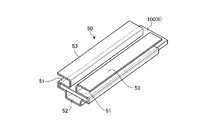
図12は、第3の実施の形態にかかる半導体装置の搬送方法に用いる保持部材の外観斜視図である。図13は、図12に示す保持部材が箱に収納された状態を示す断面図である。本実施の形態では、半導体装置100を保持部材50で梱包して搬送する。保持部材50は、経時変化による基板8の反りを抑制する。(Third embodiment)
FIG. 12 is an external perspective view of a holding member used in the method for transporting a semiconductor device according to the third embodiment. FIG. 13 is a cross-sectional view showing a state where the holding member shown in FIG. 12 is housed in a box. In the present embodiment, the
保持部材50は、挟持部51と連結部52とを備える。1つの保持部材50に対して2つの挟持部51が設けられる。挟持部51は、基板8の長手方向に沿った部分を挟み込んで保持する。基板8を両側から保持するために、1つの保持部材50に対して2つの挟持部51が設けられる。挟持部51は、断面U字状に形成されて、その隙間に基板8の長手方向に沿った部分を挟み込む。挟持部51は、経時変化に伴って基板8の長手方向に沿った反りを生じさせる力に対抗して、基板8の反りを抑制する。したがって、挟持部51は、基板8を反らせようとする力に対抗できる強度で形成される。 The holding
また、基板8の反りを抑制するために、基板8を保持している状態で、基板8に挟持部51が密着していることが好ましい。挟持部51に形成される隙間を、例えば、基板8の厚さよりも僅かに狭く形成し、その隙間を押し広げながら基板8を挟持部51に差し込むように構成してもよい。また、基板8と略等しい幅や僅かに広い幅で形成し、その隙間に簡単に基板8を差し込めるように構成してもよい。 Further, in order to suppress the warpage of the
連結部52は、2つの挟持部51を連結する。これにより、保持部材50を一体化することができる。連結部52は、図13に示すように、複数の半導体装置100を箱内に収納した際に、半導体装置100同士の間隔を保持し、搬送時に半導体装置100に加わる衝撃を緩和する緩衝材としても機能する。 The connecting
なお、挟持部51には、それぞれに間隔保持部53が形成されている。間隔保持部53は、挟持部51に対して連結部52が設けられた側の反対側に延びるように形成される。間隔保持部53は、図13に示すように、複数の半導体装置100を箱内に収納した際に、半導体装置100同士の間隔を保持し、搬送時に半導体装置100に加わる衝撃を緩和する緩衝材として機能する。 In addition, the holding |
なお、本実施の形態では、挟持部51が基板8を挟み込むとして説明しているが、基板8には、例えば抵抗やコンデンサなどの電子部品(図示せず)、NANDメモリ10などが実装される。したがって、基板8の周囲部分に電子部品などが実装されている場合には、基板8と電子部品などを合わせて挟み込むことができる幅で挟持部51を形成すればよい。 In the present embodiment, the sandwiching
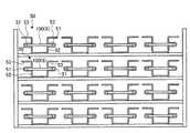
図14は、第3の実施の形態の変形例にかかる保持部材50の正面図である。本変形例では、挟持部51が固定部51aと可動部51bを有して構成される。固定部51aと可動部51bは、挟持部51に形成される隙間の底にあたる部分で回転可能に連結されており、可動部51bを開閉することができる。 FIG. 14 is a front view of a holding
可動部51bのそれぞれには、閉止部55が形成されている。閉止部55は、図14に示すように、可動部51bを閉じた際に互いに引っ掛かりあって、可動部51bが閉じた状態を保持している。また、可動部51bが閉じた状態であることで、挟持部51に形成される隙間の幅が一定に保たれる。 A closing
図15は、図14に示す保持部材50の可動部51bを開いた状態を示す図である。図15に示すように、可動部51bを開くことで、挟持部51の隙間を広げることができる。挟持部51の隙間を広げた状態で、固定部51aの上に半導体装置100を載置し、可動部51bを閉じれば、隙間を押し広げながら半導体装置100を挟持部51に差し込む場合に比べて容易に半導体装置100を保持部材50に保持させることができる。 FIG. 15 is a view showing a state in which the
1 ホスト、2 SATAインタフェース(ATA /IF)、3 通信インタフェース、4 ドライブ制御回路(コントローラ)、5 電源回路、7 温度センサ、8 基板、8a 絶縁膜、8b 配線層、9 コネクタ、9a スリット、10 NANDメモリ(NAND型フラッシュメモリ,不揮発性半導体記憶素子)、20 DRAM(揮発性半導体記憶素子)、30 中心線、31 接着部、32 スリット、50 保持部材、51 挟持部、52 連結部、53 間隔保持部、55 閉止部、100 半導体装置、200 デバッグ用機器。 1 host, 2 SATA interface (ATA / IF), 3 communication interface, 4 drive control circuit (controller), 5 power supply circuit, 7 temperature sensor, 8 substrate, 8a insulating film, 8b wiring layer, 9 connector, 9a slit, 10 NAND memory (NAND flash memory, non-volatile semiconductor memory element), 20 DRAM (volatile semiconductor memory element), 30 center line, 31 adhesive part, 32 slit, 50 holding member, 51 clamping part, 52 connecting part, 53 interval Holding unit, 55 closing unit, 100 semiconductor device, 200 debugging device.
Claims (5)
Translated fromJapanese前記多層基板の上層側表面層に設けられた不揮発性半導体記憶素子と、
前記不揮発性半導体記憶素子の表面を露出させつつ、前記不揮発性半導体記憶素子同士の隙間と、前記不揮発性半導体記憶素子と前記多層基板との隙間に充填された接着部と、を備え、
前記多層基板の下層側内層に形成された前記配線パターンのうち、前記不揮発性半導体記憶素子同士の隙間に対向する部分の少なくとも一部にスリットが形成されている半導体装置。A multilayer substrate on which a wiring pattern is formed;
A nonvolatile semiconductor memory element provided on the upper surface layer of the multilayer substrate;
While exposing the surface of the nonvolatile semiconductor memory element, the gap between the nonvolatile semiconductor memory elements, and an adhesive portion filled in the gap between the nonvolatile semiconductor memory element and the multilayer substrate,
A semiconductor device in which a slit is formed in at least a part of a portion of the wiring pattern formed in the lower layer side inner layer of the multilayer substrate that faces a gap between the nonvolatile semiconductor memory elements.
Priority Applications (26)
| Application Number | Priority Date | Filing Date | Title |
|---|---|---|---|
| JP2011058140AJP5579108B2 (en) | 2011-03-16 | 2011-03-16 | Semiconductor device |
| TW108112947ATWI700809B (en) | 2011-03-16 | 2012-02-23 | Semiconductor device |
| TW101106090ATWI505439B (en) | 2011-03-16 | 2012-02-23 | Semiconductor memory system |
| TW104125728ATWI560847B (en) | 2011-03-16 | 2012-02-23 | Semiconductor devices and memory system |
| TW110123423ATWI758200B (en) | 2011-03-16 | 2012-02-23 | Semiconductor device and wiring board |
| TW113100237ATWI854931B (en) | 2011-03-16 | 2012-02-23 | Semiconductor device |
| TW109125654ATWI733539B (en) | 2011-03-16 | 2012-02-23 | Semiconductor device |
| TW111103509ATWI831121B (en) | 2011-03-16 | 2012-02-23 | Semiconductor device |
| TW105131158ATWI613789B (en) | 2011-03-16 | 2012-02-23 | Semiconductor device and memory system |
| TW113128100ATWI882872B (en) | 2011-03-16 | 2012-02-23 | Semiconductor device |
| TW106141659ATWI660485B (en) | 2011-03-16 | 2012-02-23 | Semiconductor device |
| CN202310754750.7ACN116666351A (en) | 2011-03-16 | 2012-03-01 | Semiconductor Devices and Systems |
| CN201910505029.8ACN110246825B (en) | 2011-03-16 | 2012-03-01 | Semiconductor device and system |
| CN2012100522252ACN102682842A (en) | 2011-03-16 | 2012-03-01 | Semiconductor memory system |
| CN201610585991.3ACN105957855B (en) | 2011-03-16 | 2012-03-01 | Semiconductor device and storage system |
| US13/418,619US8873265B2 (en) | 2011-03-16 | 2012-03-13 | Semiconductor memory system |
| US14/324,683US9312215B2 (en) | 2011-03-16 | 2014-07-07 | Semiconductor memory system |
| US14/511,676US9437533B2 (en) | 2011-03-16 | 2014-10-10 | Semiconductor memory system |
| US15/254,825US9754632B2 (en) | 2011-03-16 | 2016-09-01 | Semiconductor memory system |
| US15/378,947US9859264B2 (en) | 2011-03-16 | 2016-12-14 | Semiconductor memory system |
| US15/822,039US10388640B2 (en) | 2011-03-16 | 2017-11-24 | Semiconductor memory system |
| US16/502,288US10607979B2 (en) | 2011-03-16 | 2019-07-03 | Semiconductor memory system |
| US16/800,398US11063031B2 (en) | 2011-03-16 | 2020-02-25 | Semiconductor memory system |
| US17/342,748US11705444B2 (en) | 2011-03-16 | 2021-06-09 | Semiconductor memory system |
| US18/203,693US12094866B2 (en) | 2011-03-16 | 2023-05-31 | Semiconductor memory system |
| US18/805,872US20240405010A1 (en) | 2011-03-16 | 2024-08-15 | Semiconductor memory system |
Applications Claiming Priority (1)
| Application Number | Priority Date | Filing Date | Title |
|---|---|---|---|
| JP2011058140AJP5579108B2 (en) | 2011-03-16 | 2011-03-16 | Semiconductor device |
Related Child Applications (2)
| Application Number | Title | Priority Date | Filing Date |
|---|---|---|---|
| JP2013146692ADivisionJP5458206B2 (en) | 2013-07-12 | 2013-07-12 | Semiconductor device |
| JP2014134709ADivisionJP5869058B2 (en) | 2014-06-30 | 2014-06-30 | Semiconductor device and system |
Publications (2)
| Publication Number | Publication Date |
|---|---|
| JP2012195440A JP2012195440A (en) | 2012-10-11 |
| JP5579108B2true JP5579108B2 (en) | 2014-08-27 |
Family
ID=46814626
Family Applications (1)
| Application Number | Title | Priority Date | Filing Date |
|---|---|---|---|
| JP2011058140AActiveJP5579108B2 (en) | 2011-03-16 | 2011-03-16 | Semiconductor device |
Country Status (4)
| Country | Link |
|---|---|
| US (11) | US8873265B2 (en) |
| JP (1) | JP5579108B2 (en) |
| CN (4) | CN105957855B (en) |
| TW (10) | TWI660485B (en) |
Families Citing this family (19)
| Publication number | Priority date | Publication date | Assignee | Title |
|---|---|---|---|---|
| JP5579108B2 (en) | 2011-03-16 | 2014-08-27 | 株式会社東芝 | Semiconductor device |
| KR101613388B1 (en)* | 2012-03-30 | 2016-04-18 | 히타치가세이가부시끼가이샤 | Multilayer wiring board |
| JP6039318B2 (en)* | 2012-08-31 | 2016-12-07 | 矢崎総業株式会社 | Printed wiring board |
| JP5458206B2 (en)* | 2013-07-12 | 2014-04-02 | 株式会社東芝 | Semiconductor device |
| JP5583262B2 (en)* | 2013-11-25 | 2014-09-03 | 株式会社東芝 | Semiconductor device and system |
| US9818682B2 (en)* | 2014-12-03 | 2017-11-14 | International Business Machines Corporation | Laminate substrates having radial cut metallic planes |
| US9917026B2 (en) | 2014-12-24 | 2018-03-13 | Renesas Electronics Corporation | Semiconductor device |
| KR102373543B1 (en)* | 2015-04-08 | 2022-03-11 | 삼성전자주식회사 | Method and device for controlling operation using temperature deviation in multi-chip package |
| JP2017009725A (en)* | 2015-06-19 | 2017-01-12 | ソニー株式会社 | Display device |
| JP6270805B2 (en)* | 2015-12-24 | 2018-01-31 | 東芝メモリ株式会社 | Semiconductor device and system |
| US10149377B2 (en) | 2016-06-24 | 2018-12-04 | Invensas Corporation | Stacked transmission line |
| JP2020017133A (en)* | 2018-07-26 | 2020-01-30 | キオクシア株式会社 | Storage apparatus and control method thereof |
| TWI878310B (en)* | 2019-06-26 | 2025-04-01 | 日商索尼半導體解決方案公司 | Semiconductor devices |
| WO2020260998A1 (en)* | 2019-06-28 | 2020-12-30 | 3M Innovative Properties Company | Multilayer circuit board |
| JP7653588B2 (en)* | 2019-07-04 | 2025-03-31 | パナソニックIpマネジメント株式会社 | Storage Unit |
| CN110475424B (en)* | 2019-08-28 | 2025-02-14 | 深圳市迈科龙电子有限公司 | High reliability printed circuit board suitable for intelligent wearing equipment |
| CN111935902A (en)* | 2020-09-23 | 2020-11-13 | 歌尔股份有限公司 | Printed circuit board |
| US11412610B2 (en)* | 2020-11-04 | 2022-08-09 | Juniper Networks, Inc | Apparatus, system, and method for mitigating the swiss cheese effect in high-current circuit boards |
| EP4498762A1 (en)* | 2023-07-25 | 2025-01-29 | Wolfspeed, Inc. | Multilayer printed circuit board with filling segment structures |
Family Cites Families (57)
| Publication number | Priority date | Publication date | Assignee | Title |
|---|---|---|---|---|
| JP2663649B2 (en)* | 1989-10-16 | 1997-10-15 | 松下電器産業株式会社 | Multi-chip mounting method |
| JPH0513982A (en) | 1991-07-02 | 1993-01-22 | Mitsubishi Electric Corp | Printed wiring board |
| EP0526133B1 (en)* | 1991-07-26 | 1997-03-19 | Nec Corporation | Polyimide multilayer wiring substrate and method for manufacturing the same |
| JPH07202359A (en) | 1993-12-30 | 1995-08-04 | Sony Corp | Circuit board |
| JPH07235776A (en) | 1994-02-24 | 1995-09-05 | Ricoh Co Ltd | Multilayer printed wiring board |
| JPH08195566A (en) | 1995-01-12 | 1996-07-30 | Hitachi Ltd | Multilayer electronic board, manufacturing method thereof, and arithmetic processing board |
| JPH09260795A (en)* | 1996-03-19 | 1997-10-03 | Tokin Corp | Electronic components mounting board |
| JP3267148B2 (en) | 1996-04-03 | 2002-03-18 | 富士通株式会社 | Multilayer printed wiring board and portable wireless communication device |
| JPH1032388A (en) | 1996-07-17 | 1998-02-03 | Fujitsu Ltd | Multilayer printed circuit board |
| JP3805441B2 (en) | 1996-10-18 | 2006-08-02 | 信越ポリマー株式会社 | Carrier tape |
| JP3333409B2 (en) | 1996-11-26 | 2002-10-15 | 株式会社日立製作所 | Semiconductor module |
| JP3961092B2 (en)* | 1997-06-03 | 2007-08-15 | 株式会社東芝 | Composite wiring board, flexible substrate, semiconductor device, and method of manufacturing composite wiring board |
| JPH1168313A (en) | 1997-08-11 | 1999-03-09 | Hitachi Cable Ltd | Printed wiring board |
| JP2000133941A (en) | 1998-10-28 | 2000-05-12 | Ibiden Co Ltd | Multilayer build-up wiring board |
| TW535470B (en)* | 1999-08-26 | 2003-06-01 | Mitac Int Corp | Pressing method of eight-layered circuit board and the structure thereof |
| EP1258070A2 (en)* | 2000-02-18 | 2002-11-20 | Liebert Corporation | Modular uninterruptible power supply |
| JP4514327B2 (en) | 2000-12-27 | 2010-07-28 | 京セラ株式会社 | Packaging container for semiconductor element storage package |
| JP4475825B2 (en)* | 2001-01-10 | 2010-06-09 | パナソニック株式会社 | Electronic component mounting module and substrate reinforcing method for electronic component mounting module |
| JP2002261402A (en)* | 2001-03-01 | 2002-09-13 | Alps Electric Co Ltd | Circuit board for electronic circuit unit |
| JP4318417B2 (en)* | 2001-10-05 | 2009-08-26 | ソニー株式会社 | High frequency module board device |
| JP2003218272A (en)* | 2002-01-25 | 2003-07-31 | Sony Corp | High frequency module and its manufacturing method |
| JP2003258189A (en) | 2002-03-01 | 2003-09-12 | Toshiba Corp | Semiconductor device and manufacturing method thereof |
| JP4024563B2 (en)* | 2002-03-15 | 2007-12-19 | 株式会社日立製作所 | Semiconductor device |
| US20060055501A1 (en)* | 2002-12-10 | 2006-03-16 | Bourns., Inc | Conductive polymer device and method of manufacturing same |
| WO2004053899A1 (en)* | 2002-12-11 | 2004-06-24 | Bourns, Inc. | Conductive polymer device and method of manufacturing same |
| EP1573753B1 (en)* | 2002-12-11 | 2006-05-31 | Bourns, Inc. | Encapsulated electronic device and method of manufacturing the same |
| JP4256198B2 (en)* | 2003-04-22 | 2009-04-22 | 株式会社東芝 | Data storage system |
| JP2004342934A (en) | 2003-05-16 | 2004-12-02 | Sumitomo Metal Micro Devices Inc | Printed board |
| JP2004363347A (en) | 2003-06-05 | 2004-12-24 | Oki Electric Ind Co Ltd | Multilayer printed circuit board |
| JP2005123493A (en) | 2003-10-20 | 2005-05-12 | Sony Corp | Wiring substrate and element packaging substrate |
| JP2005136232A (en)* | 2003-10-30 | 2005-05-26 | Kyocera Corp | Wiring board |
| JP4672290B2 (en) | 2004-06-16 | 2011-04-20 | 富士通株式会社 | Circuit board, package board manufacturing method, and package board |
| JP2006108289A (en)* | 2004-10-04 | 2006-04-20 | Yazaki Corp | Printed wiring board |
| KR20060060596A (en)* | 2004-11-30 | 2006-06-05 | 마츠시타 덴끼 산교 가부시키가이샤 | Semiconductor memory |
| US7009190B1 (en) | 2004-12-10 | 2006-03-07 | Eastman Kodak Company | Method and apparatus for capturing an image |
| JP2006199300A (en) | 2005-01-18 | 2006-08-03 | Matsushita Electric Ind Co Ltd | Electronic component wrapping band and manufacturing method thereof |
| JP4237160B2 (en)* | 2005-04-08 | 2009-03-11 | エルピーダメモリ株式会社 | Multilayer semiconductor device |
| JP2007134540A (en)* | 2005-11-11 | 2007-05-31 | Murata Mfg Co Ltd | Semiconductor device and manufacturing method thereof |
| JP2007149829A (en) | 2005-11-25 | 2007-06-14 | Fujifilm Corp | Electronic component mounting board |
| JP2007311723A (en)* | 2006-05-22 | 2007-11-29 | Furukawa Electric Co Ltd:The | Multilayer circuit board |
| JP2008071963A (en) | 2006-09-14 | 2008-03-27 | Denso Corp | Multilayer wiring substrate |
| JP5046720B2 (en) | 2006-12-22 | 2012-10-10 | 京セラ株式会社 | Coil built-in board |
| JP4087884B2 (en) | 2007-03-15 | 2008-05-21 | Tdk株式会社 | High frequency module |
| KR100919342B1 (en)* | 2007-09-06 | 2009-09-25 | 주식회사 하이닉스반도체 | Manufacturing Method of Semiconductor Device |
| US8378472B2 (en)* | 2007-10-17 | 2013-02-19 | Panasonic Corporation | Mounting structure for semiconductor element with underfill resin |
| JP2009152282A (en) | 2007-12-19 | 2009-07-09 | Shinko Electric Ind Co Ltd | Aggregate wiring board and semiconductor package |
| JP5161560B2 (en) | 2007-12-28 | 2013-03-13 | 株式会社東芝 | Semiconductor memory device |
| JP2009200101A (en)* | 2008-02-19 | 2009-09-03 | Liquid Design Systems:Kk | Semiconductor chip and semiconductor device |
| JP2009267162A (en)* | 2008-04-25 | 2009-11-12 | Toyota Industries Corp | Printed circuit board |
| JP2010079445A (en)* | 2008-09-24 | 2010-04-08 | Toshiba Corp | Ssd device |
| KR20100041515A (en) | 2008-10-14 | 2010-04-22 | 삼성전자주식회사 | Method for testing a solid state drive having a removable auxiliary test terminals |
| JP2010114137A (en)* | 2008-11-04 | 2010-05-20 | Toshiba Corp | Multilayer printed wiring board |
| JP2010135418A (en) | 2008-12-02 | 2010-06-17 | Shinko Electric Ind Co Ltd | Wiring board and electronic component device |
| JP2010219498A (en)* | 2009-02-20 | 2010-09-30 | Elpida Memory Inc | Semiconductor device |
| KR101037450B1 (en)* | 2009-09-23 | 2011-05-26 | 삼성전기주식회사 | Package substrate |
| US8334463B2 (en)* | 2009-10-30 | 2012-12-18 | Ibiden Co., Ltd. | Wiring board and method for manufacturing the same |
| JP5579108B2 (en)* | 2011-03-16 | 2014-08-27 | 株式会社東芝 | Semiconductor device |
- 2011
- 2011-03-16JPJP2011058140Apatent/JP5579108B2/enactiveActive
- 2012
- 2012-02-23TWTW106141659Apatent/TWI660485B/enactive
- 2012-02-23TWTW104125728Apatent/TWI560847B/enactive
- 2012-02-23TWTW110123423Apatent/TWI758200B/enactive
- 2012-02-23TWTW111103509Apatent/TWI831121B/enactive
- 2012-02-23TWTW109125654Apatent/TWI733539B/enactive
- 2012-02-23TWTW108112947Apatent/TWI700809B/enactive
- 2012-02-23TWTW105131158Apatent/TWI613789B/enactive
- 2012-02-23TWTW101106090Apatent/TWI505439B/enactive
- 2012-02-23TWTW113128100Apatent/TWI882872B/enactive
- 2012-02-23TWTW113100237Apatent/TWI854931B/enactive
- 2012-03-01CNCN201610585991.3Apatent/CN105957855B/enactiveActive
- 2012-03-01CNCN2012100522252Apatent/CN102682842A/enactivePending
- 2012-03-01CNCN201910505029.8Apatent/CN110246825B/enactiveActive
- 2012-03-01CNCN202310754750.7Apatent/CN116666351A/enactivePending
- 2012-03-13USUS13/418,619patent/US8873265B2/enactiveActive
- 2014
- 2014-07-07USUS14/324,683patent/US9312215B2/enactiveActive
- 2014-10-10USUS14/511,676patent/US9437533B2/enactiveActive
- 2016
- 2016-09-01USUS15/254,825patent/US9754632B2/enactiveActive
- 2016-12-14USUS15/378,947patent/US9859264B2/enactiveActive
- 2017
- 2017-11-24USUS15/822,039patent/US10388640B2/enactiveActive
- 2019
- 2019-07-03USUS16/502,288patent/US10607979B2/enactiveActive
- 2020
- 2020-02-25USUS16/800,398patent/US11063031B2/enactiveActive
- 2021
- 2021-06-09USUS17/342,748patent/US11705444B2/enactiveActive
- 2023
- 2023-05-31USUS18/203,693patent/US12094866B2/enactiveActive
- 2024
- 2024-08-15USUS18/805,872patent/US20240405010A1/enactivePending
Also Published As
Similar Documents
| Publication | Publication Date | Title |
|---|---|---|
| JP5579108B2 (en) | Semiconductor device | |
| JP5869058B2 (en) | Semiconductor device and system | |
| JP6511123B2 (en) | Semiconductor device | |
| JP5458206B2 (en) | Semiconductor device | |
| JP6942227B2 (en) | Semiconductor device | |
| JP5583262B2 (en) | Semiconductor device and system | |
| JP7163464B2 (en) | semiconductor equipment | |
| JP6270805B2 (en) | Semiconductor device and system | |
| JP2019125806A (en) | Semiconductor device |
Legal Events
| Date | Code | Title | Description |
|---|---|---|---|
| A621 | Written request for application examination | Free format text:JAPANESE INTERMEDIATE CODE: A621 Effective date:20130215 | |
| A977 | Report on retrieval | Free format text:JAPANESE INTERMEDIATE CODE: A971007 Effective date:20130510 | |
| A131 | Notification of reasons for refusal | Free format text:JAPANESE INTERMEDIATE CODE: A131 Effective date:20130514 | |
| A521 | Request for written amendment filed | Free format text:JAPANESE INTERMEDIATE CODE: A523 Effective date:20130712 | |
| A131 | Notification of reasons for refusal | Free format text:JAPANESE INTERMEDIATE CODE: A131 Effective date:20130924 | |
| A521 | Request for written amendment filed | Free format text:JAPANESE INTERMEDIATE CODE: A523 Effective date:20131125 | |
| TRDD | Decision of grant or rejection written | ||
| A01 | Written decision to grant a patent or to grant a registration (utility model) | Free format text:JAPANESE INTERMEDIATE CODE: A01 Effective date:20140610 | |
| A61 | First payment of annual fees (during grant procedure) | Free format text:JAPANESE INTERMEDIATE CODE: A61 Effective date:20140708 | |
| R151 | Written notification of patent or utility model registration | Ref document number:5579108 Country of ref document:JP Free format text:JAPANESE INTERMEDIATE CODE: R151 | |
| S111 | Request for change of ownership or part of ownership | Free format text:JAPANESE INTERMEDIATE CODE: R313111 | |
| R350 | Written notification of registration of transfer | Free format text:JAPANESE INTERMEDIATE CODE: R350 | |
| S111 | Request for change of ownership or part of ownership | Free format text:JAPANESE INTERMEDIATE CODE: R313111 | |
| R350 | Written notification of registration of transfer | Free format text:JAPANESE INTERMEDIATE CODE: R350 | |
| S531 | Written request for registration of change of domicile | Free format text:JAPANESE INTERMEDIATE CODE: R313531 | |
| S533 | Written request for registration of change of name | Free format text:JAPANESE INTERMEDIATE CODE: R313533 | |
| R350 | Written notification of registration of transfer | Free format text:JAPANESE INTERMEDIATE CODE: R350 |